

Page 1
N0413N
Part No.
Package
Packing
Item
Symbol
Ratings
Unit
Drain to Source Voltage (VGS = 0 V)
V
40
V
Gate to Source Voltage (VDS = 0 V)
V
GSS
±20
V
Drain Current (DC) (TC = 25°C)
I
100
A
Drain Current (pulse)
I
D(pulse)
±400
A
Total Power Dissipation (TC = 25°C)
PT1
119
W
Total Power Dissipation (TA = 25°C)
PT2
1.5
W
Channel Temperature
T
150 °C
Storage Temperature
T
stg
−55 to +150
°C
Single Avalanche Current
IAS
55
A
Single Avalanche Energy
EAS
300
mJ
Item
Symbol
Max. Value
Unit
Channel to Case Thermal Resistance
R
1.05
C/W
Channel to Ambient Thermal Resistance
R
th(ch-A)
83.3
C/W
R07DS0555EJ0200
2020.06.10
N-channel MOSFET
40 V, 100 A, 3.3 mΩ
Features
Preliminary Data Sheet
Rev.2.00
• Low on-state resistance R
• Low C
• High current I
: C
iss
= 5550 pF TYP. (VDS = 25 V, VGS = 0 V)
iss
= ±100 A
D(DC)
= 3.3 mΩ MAX. (VGS = 10 V, ID = 50 A)
DS (on)
• RoHS Compliant
• Quality Grade : Standard
• Applications : For high current switching
Ordering Information
N0413N-ZK-E1-AY TO-263, Pb-free
Note: 1. Pb-free means that this product does not contain lead in the external electrode.
Note1
800 pcs / Tape and Reel
Absolute Maximum Ratings (TA = 25°C)
DSS
D(DC)
Note2
±
ch
Note3
Note3
Note: Continuous heavy condition (e.g. high temperature/voltage/current or high variation of temperature) may affect a
reliability even if it is within the absolute maximum ratings. Please consider derating condition for appropriate
reliability in reference Renesas Semiconductor Reliability Handbook (Recommendation for Handling and Usage of
Semiconductor Devices) and individual reliability data.
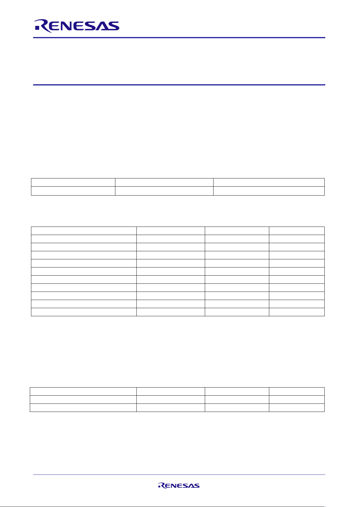
Notes: 2. PW ≤ 10
3. Starting Tch = 25°C, RG = 25 Ω, VDD = 25 V, VGS = 20 → 0 V, L = 100 µH
µ
s, Duty Cycle ≤ 1%
Thermal Resistance
Note4
°
th(ch-C)
Notes: 4. This data is the designed target maximum value on Renesas’s measurement condition. (Not tested)
°
R07DS0555EJ0200 Rev.2.00 Page 1 of 6
2020.6.10
Page 2
N0413N Chapter Title
Item
Symbol
MIN.
TYP.
MAX.
Unit
Test Conditions
Zero Gate Voltage Drain Current
I
1 µA
VDS = 40 V, VGS = 0 V
Gate Leakage Current
I
±100
nA
VGS = ±20 V, VDS = 0 V
Gate to Source Cut-off Voltage
V
2.0 4.0
V
VDS = 10 V, ID = 1 mA
Forward Transfer Admittance
Note5
| y
|
26 S VDS = 10 V, ID = 50 A
Input Capacitance
C
5550 pF
VDS = 25 V,
Output Capacitance
C
580 pF
VGS = 0 V,
Turn-on Delay Time
t
d(on)
29.0 ns
VDD = 20 V, ID = 50 A,
Rise Time
tr 15.0 ns
VGS = 10 V,
Turn-off Delay Time
t
d(off)
64.0 ns
RG = 0 Ω
Fall Time
tf 13.0 ns
Total Gate Charge
QG 100 nC
VDD = 32 V,
Gate to Source Charge
QGS 26 nC
VGS = 10 V,
Gate to Drain Charge
QGD 32 nC
ID = 100 A
Body Diode Forward Voltage
Note5
V
1.5
V
IF = 100 A, VGS = 0 V
Reverse Recovery Time
trr 40 ns
Reverse Recovery Charge
Qrr 44 nC
Electrical Characteristics (TA = 25°C)
DSS
GSS
GS(off)
R
fs
2.3 3.3 mΩ VGS = 10 V, ID = 50 A
DS(on)
iss
oss
320 pF f = 1 MHz
rss
F(S-D)
IF = 50 A, VGS = 0 V,
di/dt = 100 A/
µ
s
Drain to Source On-state Resistance
Note5
Reverse Transfer Capacitance C
Notes: 5. Pulsed test
R07DS0555EJ0200 Rev.2.00 Page 2 of 6
2020.6.10
Page 3
N0413N Chapter Title
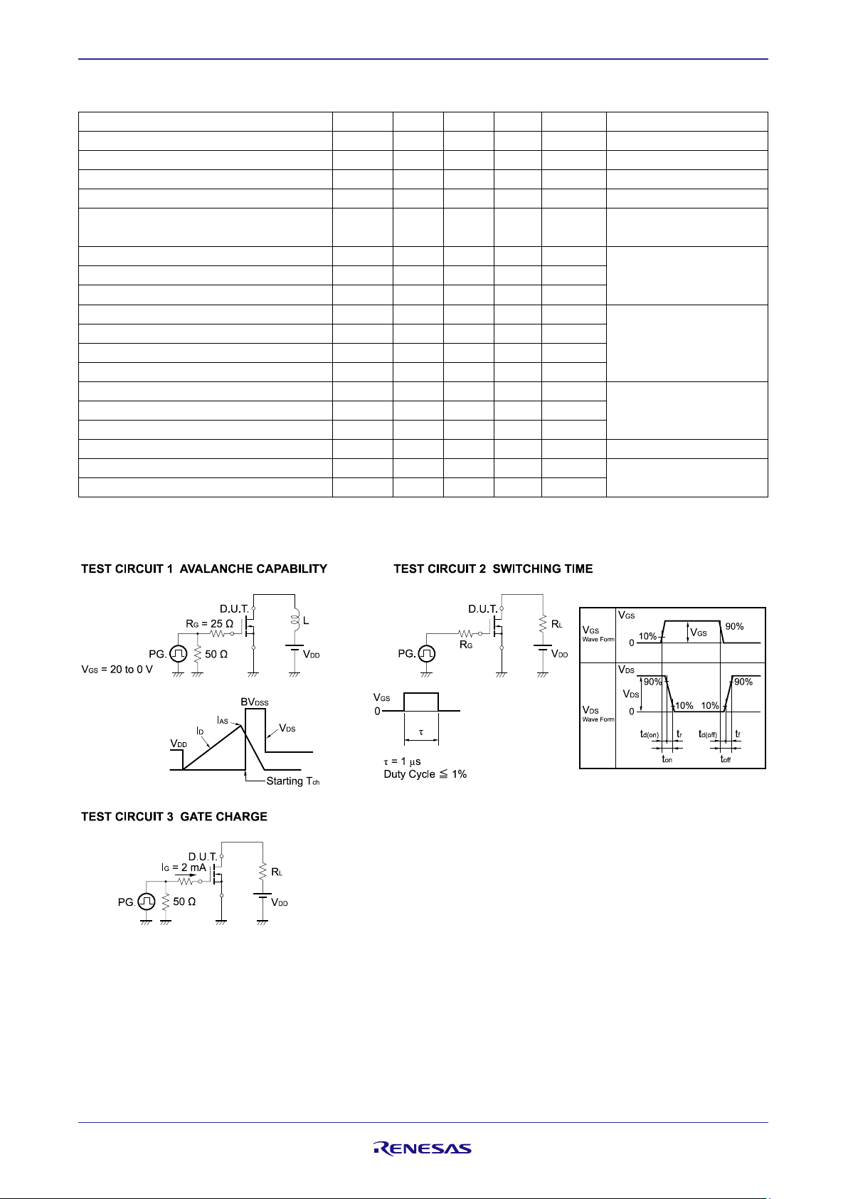
SAFE OPERATING AREA
CASE TEMPERATURE
Percentage of Rated Power
0
20
40
60
80
100
120
140
0 25 50 75
100 125
150
175
TC - Case Temperature - °C
0
20
40
60
80
100
120
140
0 25 50 75 100 125 150 175
0.1
1
10
100
1000
0.1
1 10
100
RDS(on) Limited
Power Dissipation Limited
TC = 25°C
PW = 300 µs
1 ms
10 ms
VDS - Drain to Source Voltage - V
TRANSIENT THERMAL RESISTANCE vs. PULSE WIDTH
R
th(t)
- Transient Thermal Resistance -
C/W
Single pulse
R
= 83.3°C/W
R
= 1.05°C/W
N
Note6
Typical Characteristics
DERATING FACTOR OF FORWARD BIAS
TOTAL POWER DISSIPATION vs.
- %
- Total Power Dissipation - W
T
P
dT -
FORWARD BIAS SAFE OPERATING AREA
T
- Case Temperature - °C
C
- Drain Current - A
D
I
Notes: 6. Designed target value on Renesas measurement condition. (T
8. This data is the designed target maximum value on Renesas’s measurement condition.
R07DS0555EJ0200 Rev.2.00 Page 3 of 6
2020.6.10
7. This data is the designed value on Renesas’s measurement condition. Renesas recommends that operating conditions
are designed according to a document “Power MOSFET/IGBT Attention of Handling Semiconductor Devices (R07ZZ0010)”.
ote7
1000
Note8
°
100
10
1
0.1
0.01
0.1 m 1 m 10 m 100 m 1 10 100 1000
PW - Pulse Width - s
= 25°C, unless otherwise specified)
C
th(ch-A )
TA = 25°C
th(ch-C )
Page 4

N0413N Chapter Title
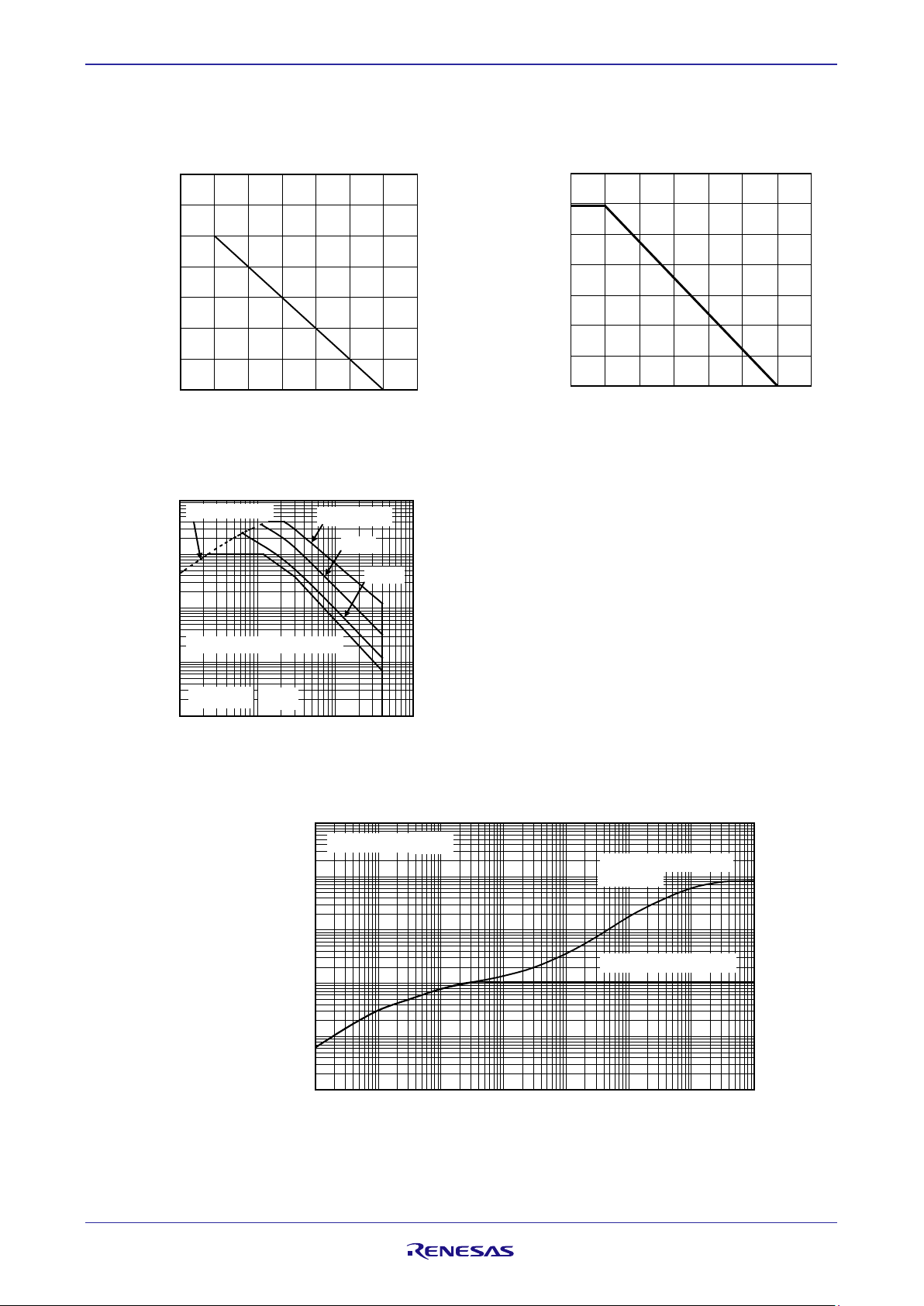
DRAIN TO SOURCE VOLTAGE
CHARACTERISTICS
0
50
100
150
200
250
300
350
400
450
0 0.2 0.4 0.6 0.8 1 1.2 1.4 1.6
VGS = 10 V
Pulsed
VDS - Drain to Source Voltage - V
0.001
0.01
0.1
1
10
100
0 1 2 3 4 5
VDS = 10 V
Pulsed
TA = 125°C
75°C
25°C
−25°C
VGS - Gate to Source Voltage - V
vs. CHANNEL TEMPERATURE
DRAIN CURRENT
0
0.5
1
1.5
2
2.5
3
3.5
-50 0 50 100 150
VDS
= 10 V
I
D
= 1.0 mA
Forward Transfer Admittance
0.01
0.1
1
10
100
0.01 0.1 1 10 100
VDS = 10 V
Pulsed
TA = 125°C
75°C
25°C
-25°C
ID - Drain Current - A
vs. DRAIN CURRENT
vs. GATE TO SOURCE VOLTAGE
Drain to Source
0
1
2
3
4
5
1 10 100 1000
Pulsed
VGS = 10 V
ID - Drain Current - A
Drain to Source On
0
5
10
15
20
25
30
35
40
0 5 10 15
20
I
D
= 50 A
Pulsed
VGS - Gate to Source Voltage - V
-25℃
DRAIN CURRENT vs.
FORWARD TRANSFER
TC=125℃
75℃
25℃
-25℃
- Drain Current - A
D
I
GATE TO SOURCE CUT-OFF VOLTAGE
- Drain Current - A
D
I
FORWARD TRANSFER ADMITTANCE vs.
- S
TC=125℃
75℃
25℃
- Gate to Source Cut-off Voltage - V
GS(off)
V
T
DRAIN TO SOURCE ON-STATE RESISTANCE
On-state Resistance - mΩ
-
DS(on)
R
R07DS0555EJ0200 Rev.2.00 Page 4 of 6
2020.6.10
- Channel Temperature - °C
ch
| -
fs
| y
DRAIN TO SOURCE ON-STATE RESISTANCE
-state Resistance - mΩ
-
DS(on)
R
Page 5

N0413N Chapter Title
vs. CHANNEL TEMPERATURE
SOURCE VOLTAGE
Drain to Source On
0
1
2
3
4
5
-50
0
50
100 150
V
GS
= 10 V
I
D
= 50 A
Pulsed
Tch - Channel Temperature - °C
10
100
1000
10000
0.1 1 10 100
V
GS
= 0 V
f = 1.0 MHz
C
rss
C
iss
C
oss
1
10
100
1000
0.1 1 10 100
V
DD
= 20 V
V
GS
= 10 V
R
G
= 0 Ω
t
d(on)
t
r
t
d(off)
t
f
0
2
4
6
8
10
12
14
0 20 40 60 80
100 120
I
D = 100 A
VDD
= 8 V
20 V
32 V
QG - Gate Charge - nC
VOLTAGE
REVERSE RECOVERY TIME vs.
0.01
0.1
1
10
100
1000
0 0.4 0.8 1.2 1.6
Pulsed
V
GS
= 10 V
0 V
Reverse Recovery Time
0.1
1
10
100
0.1 1
10 100
V
GS
= 0 V
di/dt = 100 A/µs
DRAIN TO SOURCE ON-STATE RESISTANCE
-state Resistance - mΩ
CAPACITANCE vs. DRAIN TO
- Capacitance - pF
rss
, C
oss
, C
iss
-
DS(on)
R
SWITCHING CHARACTERISTICS
C
V
- Drain to Source Voltage - V
DS
DYNAMIC INPUT CHARACTERISTICS
- Switching Time - ns
f
, t
d (off)
, t
r
, t
d (on)
t
I
- Drain Current - A
D
SOURCE TO DRAIN DIODE FORWARD
- Gate to Source Voltage - V
GS
V
DIODE FORWARD CURRENT
- ns
- Diode Forward Current - A
F
-
rr
t
I
V
- Source to Drain Voltage - V
F(S-D)
- Diode Forward Current - A
I
F
R07DS0555EJ0200 Rev.2.00 Page 5 of 6
2020.6.10
Page 6

N0413N Chapter Title
Source
Body
Diode
Gate
Drain
1
2,4
3
Package Drawing (Unit: mm)
Equivalent Circuit
R07DS0555EJ0200 Rev.2.00 Page 6 of 6
2020.6.10
Page 7

1. Descriptions of circuits, software and other related information in this document are provided only to illustrate the operation of semiconductor products and application examples. You are fully responsible for
Notice
the incorporation or any other use of the circuits, software, and information in the design of your product or system. Renesas Electronics disclaims any and all liability for any losses and damages incurred by
you or third parties arising from the use of these circuits, software, or information.
2. Renesas Electronics hereby expressly disclaims any warranties against and liability for infringement or any other claims involving patents, copyrights, or other intellectual property rights of third parties, by or
arising from the use of Renesas Electronics products or technical information described in this document, including but not limited to, the product data, drawings, charts, programs, algorithms, and application
examples.
3. No license, express, implied or otherwise, is granted hereby under any patents, copyrights or other intellectual property rights of Renesas Electronics or others.
4. You shall not alter, modify, copy, or reverse engineer any Renesas Electronics product, whether in whole or in part. Renesas Electronics disclaims any and all liability for any losses or damages incurred by
you or third parties arising from such alteration, modification, copying or reverse engineering.
5. Renesas Electronics products are classified according to the following two quality grades: “Standard” and “High Quality”. The intended applications for each Renesas Electronics product depends on the
product’s quality grade, as indicated below.
"Standard": Computers; office equipment; communications equipment; test and measurement equipment; audio and visual equipment; home electronic appliances; machine tools; personal electronic
"High Quality": Transportation equipment (automobiles, trains, ships, etc.); traffic control (traffic lights); large-scale communication equipment; key financial terminal systems; safety control equipment; etc.
Unless expressly designated as a high reliability product or a product for harsh environments in a Renesas Electronics data sheet or other Renesas Electronics document, Renesas Electronics products are
not intended or authorized for use in products or systems that may pose a direct threat to human life or bodily injury (artificial life support devices or systems; surgical implantations; etc.), or may cause
serious property damage (space system; undersea repeaters; nuclear power control systems; aircraft control systems; key plant systems; military equipment; etc.). Renesas Electronics disclaims any and all
liability for any damages or losses incurred by you or any third parties arising from the use of any Renesas Electronics product that is inconsistent with any Renesas Electronics data sheet, user’s manual or
other Renesas Electronics document.
6. When using Renesas Electronics products, refer to the latest product information (data sheets, user’s manuals, application notes, “General Notes for Handling and Using Semiconductor Devices” in the
reliability handbook, etc.), and ensure that usage conditions are within the ranges specified by Renesas Electronics with respect to maximum ratings, operating power supply voltage range, heat dissipation
characteristics, installation, etc. Renesas Electronics disclaims any and all liability for any malfunctions, failure or accident arising out of the use of Renesas Electronics products outside of such specified
ranges.
7. Although Renesas Electronics endeavors to improve the quality and reliability of Renesas Electronics products, semiconductor products have specific characteristics, such as the occurrence of failure at a
certain rate and malfunctions under certain use conditions. Unless designated as a high reliability product or a product for harsh environments in a Renesas Electronics data sheet or other Renesas
Electronics document, Renesas Electronics products are not subject to radiation resistance design. You are responsible for implementing safety measures to guard against the possibility of bodily injury, injury
or damage caused by fire, and/or danger to the public in the event of a failure or malfunction of Renesas Electronics products, such as safety design for hardware and software, including but not limited to
redundancy, fire control and malfunction prevention, appropriate treatment for aging degradation or any other appropriate measures. Because the evaluation of microcomputer software alone is very difficult
and impractical, you are responsible for evaluating the safety of the final products or systems manufactured by you.
8. Please contact a Renesas Electronics sales office for details as to environmental matters such as the environmental compatibility of each Renesas Electronics product. You are responsible for carefully and
sufficiently investigating applicable laws and regulations that regulate the inclusion or use of controlled substances, including without limitation, the EU RoHS Directive, and using Renesas Electronics
products in compliance with all these applicable laws and regulations. Renesas Electronics disclaims any and all liability for damages or losses occurring as a result of your noncompliance with applicable
laws and regulations.
9. Renesas Electronics products and technologies shall not be used for or incorporated into any products or systems whose manufacture, use, or sale is prohibited under any applicable domestic or foreign laws
or regulations. You shall comply with any applicable export control laws and regulations promulgated and administered by the governments of any countries asserting jurisdiction over the parties or
transactions.
10. It is the responsibility of the buyer or distributor of Renesas Electronics products, or any other party who distributes, disposes of, or otherwise sells or transfers the product to a third party, to notify such third
party in advance of the contents and conditions set forth in this document.
11. This document shall not be reprinted, reproduced or duplicated in any form, in whole or in part, without prior written consent of Renesas Electronics.
12. Please contact a Renesas Electronics sales office if you have any questions regarding the information contained in this document or Renesas Electronics products.
(Note 1) “Renesas Electronics” as used in this document means Renesas Electronics Corporation and also includes its directly or indirectly controlled subsidiaries.
(Note 2) “Renesas Electronics product(s)” means any product developed or manufactured by or for Renesas Electronics.
以下“注意事项”为从英语原稿翻译的中文译文,仅作为参考译文,英文版的“Notice”具有正式效力。
equipment; industrial robots; etc.
1. 本文档中所记载的关于电路、软件和其他相关信息仅用于说明半导体产品的操作和应用实例。用户如在产品或系统设计中应用本文档中的电路、软件和相关信息或将此等内容用于其他目的时,请自行负责。对
注意事项
于用户或第三方因使用上述电路、软件或信息而遭受的任何损失和损害,瑞萨电子概不承担任何责任。
2. 瑞萨电子在此明确声明,对于因使用瑞萨电子产品或本文档中所述技术信息(包括但不限于产品数据、图、表、程序、算法、应用实例)而造成的与第三方专利、版权或其他知识产权相关的侵权或任何其他索
赔,瑞萨电子不作任何保证并概不承担责任。
3. 本文档所记载的内容不应视为对瑞萨电子或其他人所有的专利、版权或其他知识产权作出任何明示、默示或其它方式的许可及授权。
4. 用户不得对瑞萨电子的任何产品进行全部或部分更改、修改、复制或反向工程。对于用户或第三方因上述更改、修改、复制或对瑞萨电子产品进行反向工程的行为而遭受的任何损失或损害,瑞萨电子概不承担
任何责任。
5. 瑞萨电子产品根据其质量等级分为两个等级:“标准等级”和“高质量等级”。 每种瑞萨电子产品的预期用途均取决于产品的质量等级,如下所示:
标准等级: 计算机、办公设备、通讯设备、测试和测量设备、视听设备、家用电器、机械工具、个人电子设备、工业机器人等。
高质量等级: 运输设备(汽车、火车、轮船等)、交通控制系统(交通信号灯)、大型通讯设备、关键金融终端系统、安全控制设备等。
除非是瑞萨电子数据表或其他瑞萨电子文档中明确指定为高可靠性产品或用于恶劣环境的产品,否则瑞萨电子产品不能用于、亦未授权用于可能对人类生命造成直接威胁的产品或系统及可能造成人身伤害的产
品或系统(人工生命维持装置或系统、植埋于体内的装置等)中,或者可能造成重大财产损失的产品或系统(太空系统、海底增音机、核能控制系统、飞机控制系统、关键装置系统、军用设备等)中。对于用
户或任何第三方因使用不符合瑞萨电子数据表、使用说明书或其他瑞萨电子文档的瑞萨电子产品而遭受的任何损害或损失,瑞萨电子概不承担任何责任。
6. 使用瑞萨电子产品时,请参阅最新产品信息(数据表、使用说明书、应用指南、可靠性手册中的“半导体元件处理和使用一般注意事项”等),并确保使用条件在瑞萨电子指定的最大额定值、电源工作电压范
围、散热特性、安装条件等范围内使用。对于在上述指定范围之外使用瑞萨电子产品而产生的任何故障、失效或事故,瑞萨电子概不承担任何责任。
7. 虽然瑞萨电子一直致力于提高瑞萨电子产品的质量和可靠性,但是,半导体产品有其自身的具体特性,如一定的故障发生率以及在某些使用条件下会发生故障等。除非是瑞萨电子数据表或其他瑞萨电子文档中
指定为高可靠性产品或用于恶劣环境的产品,否则瑞萨电子产品未进行防辐射设计。用户负责执行安全保护措施,以避免因瑞萨电子产品失效或发生故障而造成身体伤害、火灾导致伤害或损害和/或其他对公众
构成危险的事故。例如进行软硬件安全设计(包括但不限于冗余设计、防火控制以及故障预防等)、适当的老化处理或其他适当的措施等。由于对微机软件单独进行评估非常困难且不实际,所以请用户自行负
责对最终产品或系统进行安全评估。
8. 关于环境保护方面的详细内容,例如每种瑞萨电子产品的环境兼容性等,请与瑞萨电子的营业部门联系。用户负责仔细并充分查阅对管制物质的使用或含量进行管理的所有适用法律法规(包括但不限于《欧盟
RoHS指令》),并在使用瑞萨电子产品时遵守所有适用法律法规。对于因用户未遵守相应法律法规而导致的损害或损失,瑞萨电子概不承担任何责任。
9. 不可将瑞萨电子产品和技术用于或者嵌入日本国内或海外相应的法律法规所禁止生产、使用及销售的任何产品或系统中。也不可将瑞萨电子产品或技术用于(1)与大规模杀伤性武器(例如核武器、化学武器、生
物武器或运送此等武器的导弹,包括无人机(UAV))的开发、设计、制造、使用、存储等相关的任何目的;(2)与常规武器的开发、设计、制造或使用相关的任何目的;(3)扰乱国际和平与安全的任何其他目的,
并且不可向任何第三方销售、出口、租赁、转让、或让与瑞萨电子产品或技术,无论直接或间接知悉或者有理由知悉该第三方或任何其他方将从事上述活动。用户必须遵守对各方或交易行使司法管辖权的任意
国家/地区政府所公布和管理的任何适用出口管制法律法规。
10. 瑞萨电子产品的买方或分销商,或者分销、处置产品、或以其他方式向第三方出售或转让产品的任何其他方有责任事先向所述第三方通知本文档规定的内容和条件。
11. 在事先未得到瑞萨电子书面认可的情况下,不得以任何形式部分或全部再版、转载或复制本文档。
12. 如果对本文档所记载的信息或瑞萨电子产品有任何疑问,请向瑞萨电子的营业部门咨询。
(注1) 瑞萨电子:在本文档中指瑞萨电子株式会社及其控股子公司。
(注2) 瑞萨电子产品:指瑞萨电子开发或生产的任何产品。
(Rev.4.0-1 November 2017)
SALES OFFICES
Refer to "http://www.renesas.com/" for the latest and detailed information.
Renesas Electronics Corporation
TOYOSU FORESIA, 3-2-24 Toyosu, Koto-ku, Tokyo 135-0061, Japan
Renesas Electronics America Inc. Milpitas Campus
1001 Murphy Ranch Road, Milpitas, CA 95035, U.S.A.
Tel: +1-408-432-8888, Fax: +1-408-434-5351
Renesas Electronics America Inc. San Jose Campus
6024 Silver Creek Valley Road, San Jose, CA 95138, USA
Tel: +1-408-284-8200, Fax: +1-408-284-2775
Renesas Electronics Canada Limited
9251 Yonge Street, Suite 8309 Richmond Hill, Ontario Canada L4C 9T3
Tel: +1-905-237-2004
Renesas Electronics Europe GmbH
Arcadiastrasse 10, 40472 Düsseldorf, Germany
Tel: +49-211-6503-0, Fax: +49-211-6503-1327
Renesas Electronics (China) Co., Ltd.
Room 101-T01, Floor 1, Building 7, Yard No. 7, 8th Street, Shangdi, Haidian District, Beijing 100085, China
Tel: +86-10-8235-1155, Fax: +86-10-8235-7679
Renesas Electronics (Shanghai) Co., Ltd.
Unit 301, Tower A, Central Towers, 555 Langao Road, Putuo District, Shanghai 200333, China
Tel: +86-21-2226-0888, Fax: +86-21-2226-0999
Renesas Electronics Hong Kong Limited
Unit 1601-1611, 16/F., Tower 2, Grand Century Place, 193 Prince Edward Road West, Mongkok, Kowloon,
Hong Kong
Tel: +852-2265-6688, Fax: +852 2886-9022
Renesas Electronics Taiwan Co., Ltd.
13F, No. 363, Fu Shing North Road, Taipei 10543, Taiwan
Tel: +886-2-8175-9600, Fax: +886 2-8175-9670
Renesas Electronics Singapore Pte. Ltd.
80 Bendemeer Road, #06-02 Singapore 339949
Tel: +65-6213-0200, Fax: +65-6213-0300
Renesas Electronics Malaysia Sdn.Bhd.
Unit No 3A-1 Level 3A Tower 8 UOA Business Park, No 1 Jalan Pengaturcara U1/51A, Seksyen U1, 40150
Shah Alam, Selangor, Malaysia
Tel: +60-3-5022-1288, Fax: +60-3-5022-1290
Renesas Electronics India Pvt. Ltd.
No.777C, 100 Feet Road, HAL 2nd Stage, Indiranagar, Bangalore 560 038, India
Tel: +91-80-67208700
Renesas Electronics Korea Co., Ltd.
17F, KAMCO Yangjae Tower, 262, Gangnam-daero, Gangnam-gu, Seoul, 06265 Korea
Tel: +82-2-558-3737, Fax: +82-2-558-5338
© 2020 Renesas Electronics Corporation. All rights reserved.
http://www.renesas.com
Colophon 9.0
 Loading...