

Page 1
M65881AFP
Digital Amplifier Processor of S-Master* Technology
DESCRIPTION
The M65881AFP is a S-Master technique processor for digital amplifier enable to convert from multi liner-PCM digital input signal
to high precise switching-pulse digital output without analog processing.
The M65881AFP has built-in 24bit sampling rate converter and digital-gain-controller.
The M65881AFP enables to realize high precise ( X`tal oscillation accuracy.) full digital amplifier systems combining with power
driver IC.
FEATURES
•Built-in 24bit Sampling Rate Converter.
Input Signal Sampling Rate from 32KHz to 192KHz (24bit Maximum).
4 kinds of Digital Input Format.
•Built-in L/R Independent Digital Gain Control.
•Built-in Soft Mute Function with Exponential Approximate-Curve.
•Correspondence to Output for Headphone.
MAIN SPECIFICATION
•Master Clock
Primary Clock: 256Fsi/512Fsi Secondary Clock: 1024Fso/512Fso
•Input Signal Format:
MSB First Right Justified(16/20/24bit),MSB First Left Justified(24bit)
LSB First Right Justified(24bit),I
•Input Signal Sampling Rate from 32kHz to 192kHz.
•Gain Control Function:
+30dB~-∞dB (0.1dB Step until -96dB, -138dB Minimum)
•Third Order ∆Σ (16Fso:6bit/5bit,32Fso:5bit)
2
S(24bit)
OUTLINE : 42P2R
0.8mm pitch 42pin SSOP
REJ03F0004-0100Z
Rev.1.00
2003.05.08
APPLICATION
DVD Receiver, AV Amplifier
RECOMMENDED OPERATING CONDITIONS
Logic Block:1.8V±10%,PWM Buffer Block :3.3V±10%
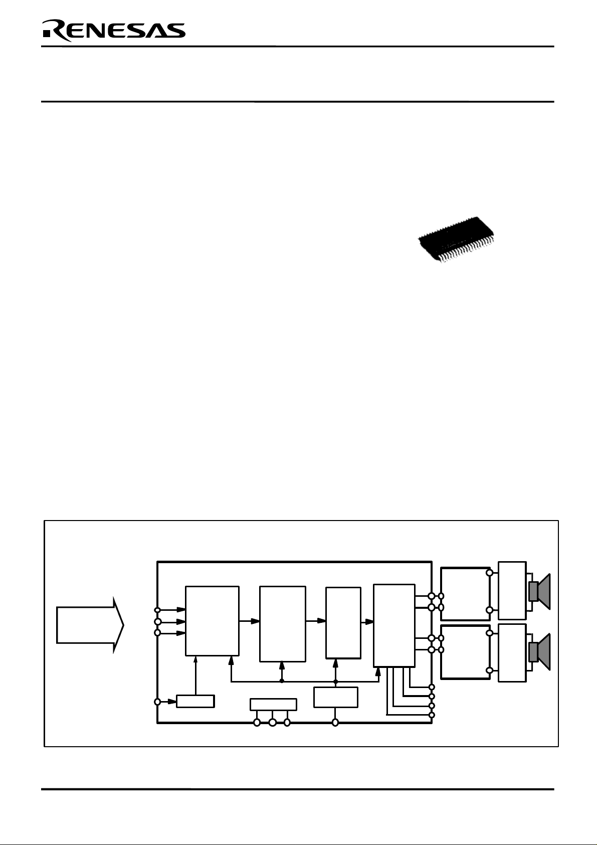
SYSTEM BLOCK DIAGRAM)
CD
DVD Audio
etc.
LRCK
BCK
DATA
256fsi/512fsi
24bit
32kHz
192kHz
Sampling
Rate
Converter
to
Clock
M65881AFP
Level
Control
+30dB
to
-∞
MCU I/F
Clock
∆Σ
PWM
Stream
Power
Driver
Stream
Power
Driver
Output
for Headphone
LC
Filter
LC
Filter
1024fso/512fso
* "S-Master" is the digital amplifier technology developed by Sony Corporation. "S-Master" is a trademark of Sony Corporation.
Rev.1.00 2003.05.08
page 1 of 23
Page 2

M65881AFP
PIN CONFIGURATION
3.3V
system
1.8V
system
VddL
OUTL1
OUTL2
XOVdd
XfsoOUT
XOVss
DVdd
DVss
MCKSEL
SCDT
1
2
3
4
5
6
7
8
9
10
11
PWM output
for Power Stage
42
41
40
39
38
37
36
35
34
33
32
VddR
OUTR1
VssRVssL
OUTR2
VssLR
XVdd
XfsoIN
XVss
HPVddL
HPOUTL1
HPVssL
3.3V
system
3.3V
system
SCSHIFT
SCLATCH
NSPMUTE
INIT
LRCK
BCK
DATA
BFVdd SFLAG
BFVss
XfsiIN FsoCKO
12
13
14
15
16
17
18
19
20
21
PWM output
for Headphone
31
30
29
28
27
26
25
24
23
22
HPOUTL2
HPVddR
HPOUTR1
HPVssR
HPOUTR2
TEST1
TEST2
FsoI
Rev.1.00 2003.05.08
page 2 of 23
Page 3
M65881AFP
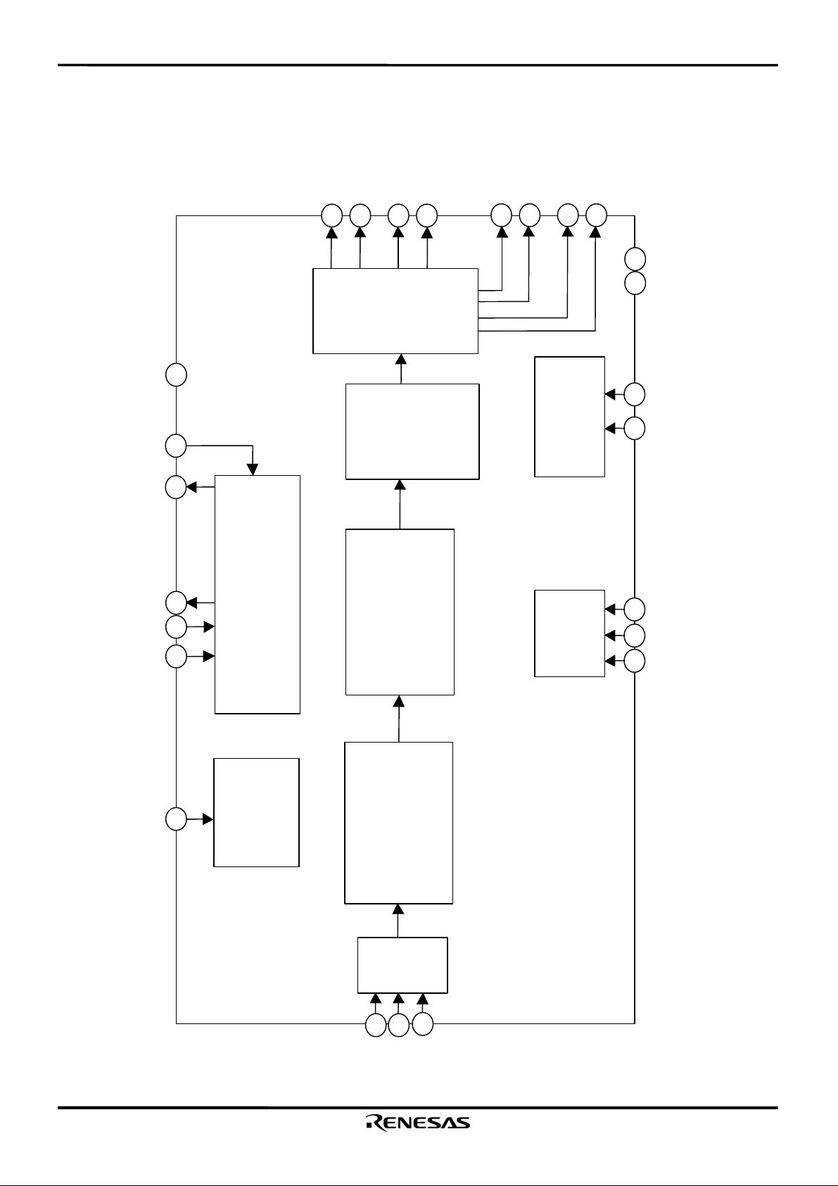
BLOCK DIAGRAM
OUTL2
4
OUTR1
OUTR2
41
39
HPOUTL1
HPOUTL2
33
31
HPOUTR1
HPOUTR2
29
27
25
26
2
T
T
T
E
S
1
T
E
S
OUTL1
2
PWM
L
F
S
f
X
A
G
24
M
T
T
E
U
S
P
N
14
I
I
I
s
o
N
36
∆Σ
15
N
INIT/MUTE
f
s
F
M
s
C
o
O
o
C
s
F
KSE
K
o
X
6
T
U
O
2210
I
23
Generator
L
Clock
( Secondary )
Gain Control
Serial
Control
11 12 13
L
T
S
S
S
A
C
C
S
H
C
T
C
D
H
I
F
T
i
f
X
Rev.1.00 2003.05.08
I
s
N
21
Clock
page 3 of 23
Generator
( Primary )
Sampling
Rate Converter
S⇒P
17
BCK
16
LRCK
18
DATA
Page 4
M65881AFP
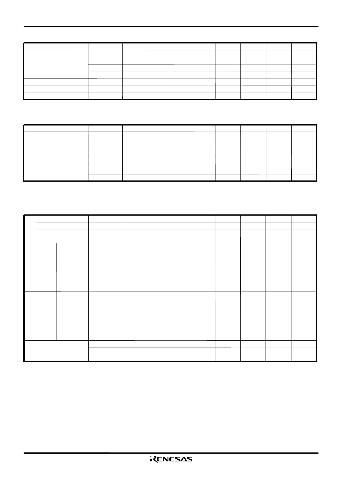
ABSOLUTE MAXIMUM RATINGS
Parameter
Supply Voltage
Input Voltage Range
Power Dissipation
Storage Temperature
Symbol Condition Min. Typ. Max Unit
PWMVdd V
3.3V system (XVdd, XOVdd, PWM Output
for Power Stage & Headphone)
BFVdd 3.3V system -0.3 – 3.8 V
DVdd 1.8V system -0.3 – 2.5 V
Vi -0.3 – Vdd+0.3 V
Pd Ta=75ºC 350 mW
Tstg -40 – 125
RECOMMENDED OPERATING CONDITIONS
Parameter
Supply Voltage
Operating Temperature
Operating Frequency
Symbol Condition
PWMVdd
3.3V system (XVdd, XOVdd, PWM Output
for Power Stage & Headphone)
BFVdd 3.3V system
DVdd 1.8V system
Ta
XfsoIN
XfsiIN
-0.3 – 3.8
Min. Typ. Max
3.0 3.3
3.0 3.3 3.6
1.6 1.8 2.0
-20
16 52.5
8 25
–
–
–
3.6
75
ºC
Unit
V
V
V
ºC
MHz
MHz
ELECTRICAL CHARACTERISTICS
Parameter
"H" Level Input Voltage
"L" Level Input Voltage
Input Leek Current
"H" Level Output
Voltage
"L" Level Output
Voltage
Power Supply Current
XfsoOUT
SFLAG
FsoCKO
OUTL1,2
OUTR1,2
HPOUTL1,2
HPOUTR1,2
XfsoOUT
SFLAG
FsoCKO
OUTL1,2
OUTR1,2
HPOUTL1,2
HPOUTR1,2
Symbol Conditions
VIH3 BFVdd=3.0 to 3.6V
VIH3 BFVdd=3.0 to 3.6V
Ileak
VOH3 Vdd-0.5 – –
VOL3 – – 0.5
Idd2 1.8V system (DVdd)
Idd3 – 2.5
(Ta=25ºC,PWMVdd=3.3V, DVdd=1.8V : Unless otherwise specified.)
Min. Typ. M
0.75Vdd – –
– – 0.25Vdd
– – 10
BFVdd=3.0 to 3.6V
IOH3=-4.0mA (SFLAG,FsoCKO)
IOH3=-2.0mA (XfsoOUT,OUTL1,2,OUTR1,2)
IOH3=-1.0mA (HPOUTL1,2,HPOUTR1,2)
BFVdd=3.0 to 3.6V
IOL3=4.0mA (SFLAG, FsoCKO)
IOL3=2.0mA (XfsoOUT,OUTL1,2,OUTR1,2)
IOL3=1.0mA (HPOUTL1,2,HPOUTR1,2)
–
3.3V system (PWMVdd, BFVdd)
OUTxx, HPOUTxx="OPEN"
3.5
Unit
µA
V
V
–
– mA
mA
V
V
Rev.1.00 2003.05.08
page 4 of 23
Page 5
M65881AFP
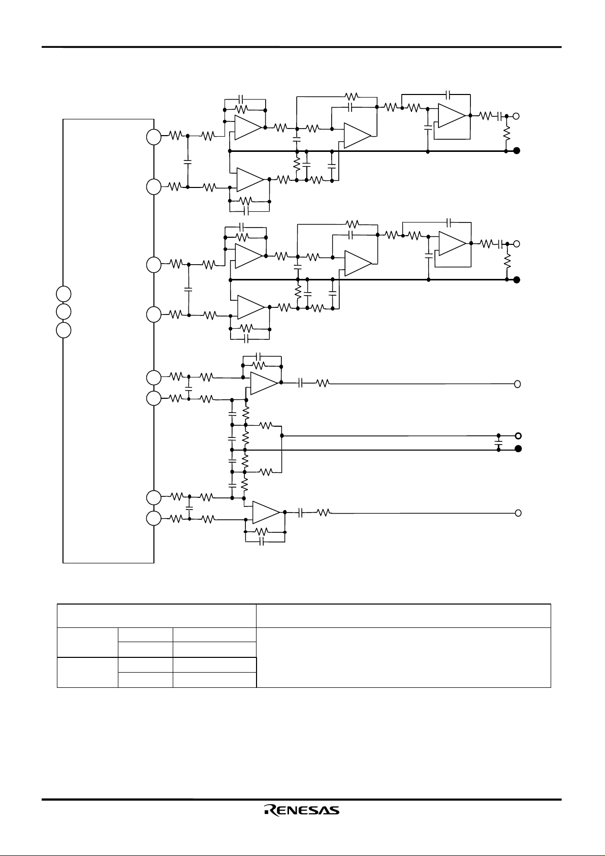
CHARACTERISTICS EVALUATION CIRCUIT
-
OUTL1
2
+
+
OUTL2
4
-
-
OUTR2
39
+
+
-
-
+
GND
+
-
+
-
LRCK
BCK
DATA
16
17
18
OUTR1
M65881AFP
HPOUTL1
HPOUTL2
HPOUTR2
HPOUTR1
41
33
31
27
29
+
GND
-
-
+
Power Supply
GND
+
-
Reference characteristic
Output for
Power Stage
Output for
Headphone
Rev.1.00 2003.05.08
THD+N
THD+N
S/N
S/N
page 5 of 23
102dB(typ)
0.002%(typ)
100dB(typ)
0.006%(typ)
Conditions
• Input :1kHz 0dB Full scale sine wave
• FS :Primary clock 44.1kHz, Secondary clock 48kHz
• PWM Output format 1 • AC dithering E • DC dithering : 0.1%
• Gain data setting : (Index) 10000b/ (Mantissa) 10000000b
• THD+N: Filter 20kHz LPF S/N: Filter 22kHz LPF + JIS-A
Page 6
M65881AFP
PIN DESCRIPTION
Pin No. Name I/O
1 VddL
2 OUTL1 O
3 VssL
4 OUTL2 O
5 XOVdd
6 XfsoOUT O
7 XOVss
8 DVdd
9 DVss
10 MCKSEL I
11 SCDT I
12 SCSHIFT I
13 SCLATCH I
14 NSPMUTE I
15 INIT I
16 LRCK I
17 BCK I
18 DATA I
19 BFVdd
20 BFVss
21 XfsiIN I
22 FsoCKO O
23 FsoI I
24 SFLAG O
25 TEST2 I
26 TEST1 I
27 HPOUTR2 O
28 HPVssR
29 HPOUTR1 O
30 HPVddR
31 HPOUTL2 O
32 HPVssL
33 HPOUTL1 O
34 HPVddL
35 XVss
36 XfsoIN I
37 XVdd
38 VssLR
39 OUTR2 O
40 VssR
41 OUTR1 O
42 VddR
Output
Current
Description
Power Supply for Lch PWM Power Stage (3.3V)
Lch PWM1 Output for Power Stage 3.3V
GND for Lch PWM Power Stage
Lch PWM2 Output for Power Stage 3.3V
Power Supply for Secondary Master Clock Buffer ( 3.3V )
Buffered Output of Secondary Master Clock (1024/512fso) 2mA 3.3V
GND for Secondary Master Clock Buffer
Power Supply for Digital Block (1.8V)
GND for Digital Block
Secondary Master Clock Selector "L":1024fso, "H":512fso 3.3V
Serial Control • Data Input 3.3V
Serial Control • Shift Clock Input 3.3V
Serial Control • Latch Signal Input 3.3V
PWM Duty 50% Mute ( "L": Active ) 3.3V
Initialize Input ( Power Supply Reset ) ; "L" : Reset, "H" : Release 3.3V
LRCK Input (PCM Signal ) 3.3V
BCK Input ( PCM Signal ) 3.3V
DATA Input ( PCM Signal ) 3.3V
Power Supply for Input/Output 3.3V Buffer
GND for Input/Output 3.3V Buffer
Primary Master Clock Input (256fsi/512fsi ) 3.3V
Secondary Fso Clock Output 4mA 3.3V
Secondary Fso Clock Input 3.3V
Asynchronous Flag ( H: Active ) 4mA 3.3V
Test2 must be connected to GND 3.3V
Test1 must be connected to GND 3.3V
Rch PWM2 Output for Headphone 3.3V
GND for Rch Headphone
Rch PWM1 Output for Headphone 3.3V
Power Supply for Rch Headphone ( 3.3V )
Lch PWM2 Output for Headphone 3.3V
GND for Lch Headphone
Lch PWM1 Output for Headphone 3.3V
Power Supply for Lch Headphone ( 3.3V )
GND for Secondary Master Clock Input Buffer
Secondary Master Clock Input (1024fso/512fso) 3.3V
Power Supply for Secondary Master Clock Buffer ( 3.3V )
GND for PWM Power Stage
Rch PWM 2 Output for Power Stage 3.3V
GND for Rch PWM Power Stage
Rch PWM 1 Output for Power Stage 3.3V
Power Supply for Rch PWM Power Stage ( 3.3V)
on 3.3V
–
–
–
–
–
–
–
–
–
–
–
–
–
–
–
–
–
–
–
–
–
–
–
–
–
–
–
–
–
–
–
Signal Level
–
–
–
–
–
–
–
–
–
–
–
–
–
–
–
–
–
Rev.1.00 2003.05.08
page 6 of 23
Page 7
M65881AFP
EXPLANATION OF OPERATION
1. DATA,BCK,LRCK
DATA,BCK, and LRCK are input pins for Digital Audio Signal of CD, MD, DVD etc..
Input formats are supported by 4 ways, and are set by Serial Control, "System1 Mode, bit3 and bit4".
Input data length are selectable in a case of "MSB First Right Justified"
(Serial Control "System1 Mode,bit5 and bit6").
•Input formats are shown in following figures.
MSB first left justified
(24bit)
MSB first right justified
(16bit, 20bit, 24bit)
LRCK
BCK
DATA
(24bit)
LRCK
BCK
DATA
(16bit)
DATA
(20bit)
DATA
(24bit)
MSB
MSB
1/fsi, 1/2fsi, 1/4fsi
Left Right
LSB
24cycle
Left
MSB
16 cycle
MSB
20 cycle
24 cycle 24 cycle
MSB
1/fsi, 1/2fsi, 1/4fsi
LSB
LSB
LSB
MSB
24cycle
MSB
MSB
LSB
Right
LSB
16 cycle
LSB
20 cycle
LSB
LSB first right justified
(24bit)
I2S(24bit)
LRCK
BCK
DATA
(24bit)
LRCK
BCK
DATA
(24bit)
1 BCK
1/fsi, 1/2fsi, 1/4fsi
Left Right
MSB
24 cycle 24 cycle
1/fsi, 1/2fsi, 1/4fsi
Left
LSB LSB
24 cycle
LSBLSB
1 BCK
MSBMSB
MSB
Right
24 cycle
Rev.1.00 2003.05.08
page 7 of 23
Page 8

M65881AFP
2. SCDT, SCSHIFT, SCLATCH
SCDT, SCSHIFT and SCLATCH are input pins for setting M65881AFP's operation.
Input format of SCDT, SCSHIFT and SCLATCH is shown below.
Input Format of SCDT, SCSHIFT and SCLATCH
SCDT
SCSHIFT
SCLATCH
• Mode Setting
The operating mode are classified in four and assigned by bit1 and bit2. These four functions are shown below.
( bit1 and bit2 )= ( "L" and "L" ) Gain control mode: Gain control.
( bit1 and bit2 ) = ( "L "and "H" ) System1 Mode: Primary block initialization, etc.
( bit1 and bit2 )= ( H and "L" ) System2 Mode : Secondary block initialization, etc.
( bit1 and bit2 ) = ("H" and "H" ) Test mode ( setting prohibition )
Refer to Page13 about these four setting in detail.
3. MCKSEL, XfsoIN, XfsoOUT
XfsoIN pin is secondary master clock input.
The setting of MCKSEL pin selects secondary master clock.
XfsoOUT pin is buffered-output from XfsoIN pin's input clock.
4. XfsiIN
XfsiIN pin is primary master clock input.
The frequency of primary master clock must be selected by serial control “System2 mode :bit3 (IMCKSEL)”
MCKSEL XfsoIN
"L"
"H" 512fso
bit3 (IMCKSEL) XfsiIN
"H" 512fsi
"L" 256fsi
1024fso
bit1
1510152024
The relations between input signal sampling rate and master clock frequency.
Input sampling rate
1fsi : 32k / 2fsi : 64k / 4fsi : 128k
1fsi : 44.1k / 2fsi : 88.2k / 4fsi : 176.4k
1fsi :48k / 2fsi : 96k / 4fsi : 192k
Input signal and primary clock are related to synchronization. The primary clock frequency are
512 or 256 times as much as the input signal fsi ( 32k, 44.1k and 48k.)
The primary and secondary clock are related to independence. ( asynchronization )
At 1024fso setting, secondary clock= frequency range from 32.768MHz to 49.152MHz.
At 512fso setting, secondary clock = frequency range from 16.384MHz to 24.576MHz.
*Primary clock
This clock means input side clock system of sampling rate converter.
*Secondary clock
This clock means output side clock system of sampling rate converter.
This clock makes to operate after sampling rate converter block.
(Gain Control Block and PWM Block, etc.)
*“fsi” and “fso” are defined as following stated in this specification.
fsi : Primary sampling frequency
fso : Secondary sampling frequency
Primary clock Secondary clock
512fsi/256fsi[Hz] 1024fso/512fso[Hz]
16.384M/8.192M
22.579M/11.290M
24.576M/12.288M
32.768M/16.384M
| / |
49.152M/24.576M
Rev.1.00 2003.05.08
page 8 of 23
Page 9

M65881AFP
5. FsoCKO
6. FsoI, SFLAG
FsoCKO is clock output pin of 1fso frequency. The output is divided-clock of XfsoIN, and frequency
is free-running at power on. FsoCKO pin's clock is utilized for a synchronization in case that
have used plural M65881AFP, take a synchronization between M65881AFP and other external
devices.
Refer to the following Chapter 6. in detail.
M65881AFP synchronizes in clock input from the external source devices. So it makes synchronized
operation between source devices or another M65881AFP ( in case of Multi channel Operation ).
The primary side operation ( input side of sampling rate converter ) are synchronized in LRCK, and the
secondary side operation ( output side of sampling rate converter ) are synchronized in FsoI.
M65881AFP detects rise edge of these synchronized clock in normal operation, and the M65881AFP
does operation of resynchronization in case that the cycle has changed.
In addition, the M65881AFP re-synchronizes for a synchronized clock, in case that M65881AFP detects
SYNC flag (Serial Control, System2 Mode,bit6) rise edge, too.
While re-synchronizing, SFLAG pin outputs "H" and data is muted inside.
In case of using Multiplex ( for multi channel application) and Single ( for 2ch application ), detail
explanation is shown below.
Multiplex use
Primary side: Synchronize with LRCK. All ICs synchronize with an source device by connecting
common LRCK.
Secondary side: Synchronize with FsoCKO of Master IC. One of M65881AFP becomes a master IC,
and the synchronization between ICs is carried out by FsoCKO of Master IC.
FsoCKO pin outputted from this master IC is entered each Fsol pins of master
and slave ICs.
ASYNCEN2=enable
LRCK (Primary side)
Master
LRCK
FsoCKO(Secondary side)
Fsol
Slave
LRCK
Fsol
Slave
LRCK
Fsol
Multiplex use (6ch)
Single use
Primary side: Synchronize with LRCK. Therefore M65881AFP synchronizes with source devices.
Secondary side: There is no need for external devices and other ICs to synchronize,
therefore FsoCKO is connected to FsoI, In other way,
By setting secondary side asynchronous detection to “disable” with
“ASYNCEN2” flag (Serial Control, System2 mode,bit8),
FsoI can also be considered as fixation.
ASYNCEN2=enable
LRCK (Primary)
LRCK
Fsol
FsoCKO
LRCK (Primary)
ASYNCEN2=disable
LRCK
Fsol
Rev.1.00 2003.05.08
page 9 of 23
Page 10

M65881AFP
7. OUTL1, OUTL2, OUTR1, OUTR2
OUTL1, OUTL2, OUTR1 and OUTR2 are pulse output modulated ∆Σ output to PWM signal.
These pins are connected to external Power Driver ICs.The PWM output can be selected
PWM Output Format 1, 2, 3 and 4 by serial control data(System1 mode, bit22,23 ).
PWM Output Form1 : General Modulation
PWM Output Form2 : Symmetrical Modulation
PWM Output Form3 : Modulation returned with time domain.
( The rise and fall edge of Lch and Rch in a term are reverse.)
PWM Output Form4: Modulation returned with time domain.
( The rise and fall edge of Lch and Rch in a term are same timing.)
In each 4 forms, the rate and bit length of PWM Output can be changed.
Moreover, an output mute function and an output pins reverse function
can be controlled by the pin setting or serial control.
Refer to pin setting of the following page about a phase of the PWM output
for Power Stage and Headphone.
The PWM output control is shown in the following table.
PWM output control
Item
Output Form
( Common setting for Power
Stage and Headphone)
Operating Rate
and Data Bit Length
( Common setting for
Power Stage and
Headphone )
Output Muting
( Common setting for
Power Stage and
Headphone )
Reverse Output
Pins Function
Operation
Output Form Selection
1,2,3,4
Select to
16fso/6bit ,16fso/5bit ,32fso/5bit
from operating rate and data bit
length of ∆Σ.
PWM operation are synchronized
by this setting.
Duty 50% Mute
( Selectable common and
independent setting for Lch/ Rch.)
Absolute Zero Mute
Reverse on Lch and Rch of
output pins (Common setting for
Power Stage and Headphone)
Setting Operation
Set up by the serial control system 1 mode
bit 22,23 (PWM MODE 0 and 1).
(Refer to system 1 mode(Page16) for details)
Set up by the serial control system 2 mode bit16
and bit17.
( Refer to system 2 mode(Page 18) for details.)
< Common setting for Lch / Rch >
Set NSPMUTE pin "L" or set up by serial control "
System 2 mode bit14 (NSPMUTE) "H".
< Independent Setting for Lch / Rch >
Set up by serial control Gain Control Mode bit9,10
(NSPMUTEL,NSPMUTER) "H" .
( Refer to Page 11,18 and 13 for details)
Set up by serial control system2 mode
bit15(PGMUTE) "H".
(See system2 mode(Page 18) )
Set up by serial control system2 mode bit9
(CHSEL).
Rev.1.00 2003.05.08
page 10 of 23
Reverse for R1 and R2 of
output pins.
( Only enable for Power Stage.)
Set up by serial control system2 mode bit12
(CHRSEL).
Page 11

M65881AFP
8. HPOUTL1, HPOUTL2, HPOUTR1, HPOUTR2
HPOUTL1, HPOUTL2, HPOUTR1 and HPOUTR2 are output pins for Headphone output.
PWM output modulated ∆Σ output data to pulse width.
The Phase of PWM Output for Power Stage and PWM Output for Headphone.
The output for Headphone is reverse phase as output for Power.
Moreover, it is possible to set L1 and R1 output same phase by serial control the system 1 mode,
bit24= "H"( PWMHP ).
In addition, NSPMUTE, PGMUTE and CHSEL are set in common PWM for Power
and PWM for Headphone, and as for CHRSEL flag is set as a function of only PWM for Power.
( Refer to previous page "Table of PWM control" for details ).
9. NSPMUTE
NSPMUTE pin sets to PWM Output to Duty 50% Mute.
L: PWM Output 50% Mute
H: Mute release
10. INIT
INIT is the pin for reset to all functions of M65881AFP.
"L" level: (1) Clear of data memory, (2) Initialization of a serial control setting
(3) PWM Output Duty 50% Mute
( " L" period needs more than 5msec.)
"H" level : Usual operation.
*The rise edge from "L" to "H": Re-synchronization are operated, which is same at serial control SYNC
function. (system2 mode bit6)
11. TEST1, TEST2
TEST1 and TEST2 pins are test input for factory shipping test of M65881AFP.
TEST1 and TEST2 pins must be tied to "L" level on usual operation.
12. Power supply and GND
Power supply and GND routes have a following 6 isolated lines.
(1) VddL, VssL,VddR, VssR, VssLR
VddL, VssL,VddR, VssR and VssLR pins are Power supply and GND for PWM Output buffer.
Lch and Rch have a independent power supply and GND. Power supply must be fixed at 3.3V.
(2) HPVddL, HPVssL, HPVddR, HPVssR
HPVddL, HPVssL, HPVddR and HPVssR pins are Power supply and GND of PWM Output
buffer for Headphone. Lch and Rch have a independent power supply and GND.
Power supply must be fixed at 3.3V.
(3) XVdd, XVss
XVdd and XVss are Power supply and GND for XfsoIN clock input block.
Power supply voltage must be fixed at 3.3V.
(4) XOVdd, XOVss
XOVdd and XOVss are Power supply and GND for XfsoOUT Clock Output.
Power supply voltage must be fixed at 3.3V
(5) DVdd, DVss
DVdd, DVss are Power supply and GND for internal digital block.
Power supply voltage must be fixed at 1.8V.
(6) BFVdd, BFVss
BFVdd and BFVss are Power and GND for input/output buffer (except for PWM block
and clock buffer). Power supply voltage must be fixed at 3.3V.
Rev.1.00 2003.05.08
page 11 of 23
Page 12

M65881AFP
13. Power sequences
System power-on sequencing * Refer to following figure.
Power(Vddxxx, HPVddxxx,
XVdd, XOVdd, DVdd, BFVdd)
Power OFF
Power ON
Master clock
(XfsoIN,XfsiIN)
INIT
SCDT
SCSHIFT
SCLATCH
*1 After a power supply and Master clock become to stable, INIT pin must be "L" over 5msec.
*2 Data transfer is possible right after INIT release.
*3 Until SCLATCH is operated, a period over 2/fso ( fso=48kHz, over 42µsec ) is necessary after INIT release.
X
X
Over 5msec(*1)
X
Over 0sec(*2)
X
X
Over 2/fso(*3)
Rev.1.00 2003.05.08
page 12 of 23
Page 13

M65881AFP
SERIAL CONTROL
1. Gain Control Mode
bit Flag name Functional Explanation H L
1 MODE1 Mode setting1 "L" fixed
2 MODE2 Mode setting2 "L" fixed
3 TEST1 Test Mode 1 "L" fixed
4 TEST2 Test Mode 2 "L" fixed
5 NSLMT1 Output Limit 1
6 NSLMT2 Output Limit 2
7 GCONT1 Channel selection for Gain Control Block 1 L/R Independence L/R Common
8 GCONT2 Channel selection for Gain Control Block 2 Lch Rch
9 NSPMUTEL
10 NSPMUTER
11
12 GAIN0 Gain Data Index (MSB)
13 GAIN1 Gain Data Index
14 GAIN2 Gain Data Index
15 GAIN3 Gain Data Index
16 GAIN4 Gain Data Index (LSB)
17 GAIN5 Gain Data Mantissa (MSB)
18 GAIN6 Gain Data Mantissa
19 GAIN7 Gain Data Mantissa
20 GAIN8 Gain Data Mantissa
21 GAIN9 Gain Data Mantissa
22 GAIN10 Gain Data Mantissa
23 GAIN11 Gain Data Mantissa
24 GAIN12 Gain Data Mantissa (LSB)
Lch Duty 50% Mute for PWM Output
Rch Duty 50% Mute for PWM Output
Refer to Table 1-1.
active non-active
active non-active
•Output Limit (bit5,6: NSLMT1,2)
The M65881AFP has Over Flow Limit function which detects by input signal level and limit gain control.
The limit Value is set by Gain control Mode ( bit5,6 "NSLMT1, 2") and System2 Mode( bit17 "NSOBIT").
No setting bits means " Don't care".
INIT
–
–
L
L
L
L
L
L
L
L
–
H
L
L
L
L
H
L
L
L
L
L
L
L
•Limit value setting of output for gain control and ∆Σ (bit5, 6 : NSLMT1, 2)
Table 1-1a Limit Value [ In case of 6bit mode, system2 mode bit 17( NSOBIT )="L".]
NSLMT1,2
(L, L)
(H, L)
(L, H)
(H, H)
Output Limit Value of gain
±0.9375
±0.90625
±0.875
±0.84375
PWM Output (Limit Value from ∆Σ Block)
63 values (±31)
61 values (±30)
59 values (±29)
57 values (±28)
Table 1-1b Limit Value [ In case of 5bit mode, system2 mode bit 17( NSOBIT )="H".]
NSLMT1,2
(L, L)
(H, L)
(L, H)
(H, H)
Output Limit Value of gain
±0.90625
±0.875
±0.84375
±0.8125
PWM Output ( Limit Value from ∆Σ Block)
31 value (±15)
31 value (±15)
29 value (±14)
29 value (±14)
•Channel selection for Gain Control Block (bit7,bit8: GCONT1, GCONT2)
These bit selection enable to control gain data "L/R common" or "L/R independence".
GCONT1:"L"… L/R common "H"...L/Rch independence.
GCONT2:"L"… Rch only "H"…Lch only
Bit8 is enable only the case of " Bit7="H".
•PWM Duty 50% Mute (bit9,10:NSPMUTEL,R)
*Enable both output for Power and Headphone.
These bit set "Duty 50% fixed Mute" with Lch/Rch independence.
NSPMUTEL : "L"….Mute release, "H"…Lch Mute
NSPMUTER : "L"….Mute release, "H"…Rch Mute
* Duty 50 % Mute Operation are operated by one of the following setting.
• Gain control bit9,10 ( NSPMUTEL,R)
• NSPMUTE pin
• Serial control system2 mode ,bit 14 (NSPMUTE)
Rev.1.00 2003.05.08
page 13 of 23
Page 14

M65881AFP
The index and Mantissa part of Gain Data (bit12-bit24 :GAIN0-GAIN12)
The gain value is set from bit12-bit24.
Index part: bit12(MSB) to bit16(LSB)
Mantissa part: bit17(MSB) to bit24(LSB)
The gain data is assigned 13bits, composed of Index part 5bits and of Mantissa part 8bits.
The range of Index parts is following statements.
Index part: 10100b(16.0) to 10000b(1.0) to 00000b(2
The range of Mantissa parts is following statements.
Mantissa part:Index part; 10100b to 00001b: Mantissa part; 11111111b to 10000000b (128 step/ Index).
Index part; 00000b: Mantissa part; 11111111b to 00000000b (256 step).
Initial value: Index part: 10000b Mantissa part: 10000000b
Infinity zero: Index part: 00000b Mantissa part: 00000000b
# Notice of GAIN value setting continuously
In case of Gain value setting continuously, for example of setting L/Rch independently, please take
the interval time (pulse interval time of SCLATCH signal) more than 1/fso. For example, in the case of
fso=48kHz, please take the interval time more than 21µsec.
• The Gain Data and Audio Output Level.
Gain data consists of 13bits (Index part: 5bit, Mantissa part: 8bit ).
e.g. 10000b(1.0)/10000000b(0.5) means 0.5(0dB).
Table 1-2 Gain data and output level
PolarityGain Data
-16
)
Output absolute
maximum value
Output Level
10100/11111111 (b)
~
10001/10000000 (b)
~
10000/10000000 (b)
01111/11111111 (b)
00000/10000000 (b)
00000/00000001 (b)
00000/00000000 (b)
• Calculation method of Gain Value
The way to calculation of Gain value from Gain Data is following equation.
Gain value = 20log
~~
<Index data (decimal value)-16>
[
2
+
15.9375
~~
1.0
0.5
0.498046875
~~
-16
0.5 ∗ 2
0.00390625 ∗ 2
infinity zero
×
Mantissa Data (decimal value)
-16
+30.069dB
+6.021dB
0dB
-0.0340dB
-96.330dB
-138.474dB
128
~~~~
dB
]
Rev.1.00 2003.05.08
page 14 of 23
Page 15

M65881AFP
• Soft Mute
The Soft Mute function is executed by setting of Gain Data as 00000/00000000b
(" / " means dividing point between index part and mantissa part).
The release from Soft Mute Function must be executed by setting the gain data before soft mute.
The Soft mute Function and release from there don't have linear curve but
have characteristics of approximate exponential curve.
Output amplitude
16.0
0.5
T = xxxx/Fs (sec)
0
T
00000/00000000b setting
//
T
10000/10000000b setting
Characteristics of Soft Mute function
• Operating time of Soft Mute
Total steps from Maximum value(10100b/11111111b) to Minimum value(00000b/00000000b)
(128steps/1 index) × (20index (10100b-10000b)) +256steps = 2816steps.
The transition term of up and down depend on 2fso clock.
Therefore, in case of fso=48kHz, T=1/2fso=10.416µsec/step, transition term are following.
From Maximum value (10100b/11111111b) to Minimum value (00000b/00000000b) : 2816T=29.333msec.
From 0dB value (10000b/10000000b) to Minimum value (00000b/0000000b) : 2304T=24msec
6dB transition term (when over 00000b/10000000b (=-96dB) value ) : 128T=1.333msec.
• Soft Attenuate
Transition from older Gain Attenuation to newer Gain Attenuation always operates with Soft Mute function.
For example, in case of Gain1 > Gain3 > Gain2, transition process is shown below.
At first, GAIN1 is operated, then second, GAIN2 is operated.
In case that GAIN2 is operated faster than GAIN1 of transition completion (refer to "A" situation in figure)
GAIN1 is ignored and data approaches at GAIN2.
Further, GAIN3 is operated faster than GAIN2 of transition completion( Refer to "B" or "C" situation in figure),
GAIN2 is ignored and data approaches at GAIN3
.
t
Gain
1.0
0
-1.0
Rev.1.00 2003.05.08
page 15 of 23
A
(GAIN1)
B
(GAIN3)
C
(GAIN2)
t
Soft Attenuate
Page 16

M65881AFP
2. System1 Mode
No setting bits means "Don't care".
bit Flag name Function Explanation H L
1 MODE1
2 MODE2
3 IFMT0
4 IFMT1
5 IBIT0
6 IBIT1
7 ISF0
8 ISF1
9 EMPFS1
10 EMPFS2
11 DF1IMUTE Zero Mute at DATA input
12 DF2IMUTE
Mode Setting 1
Mode Setting 2
Input Format Selection
Setting for Input Word Length
Input sampling rate selection
Fsi selection for De-emphasis Filter
Zero Mute at sampling rate converter input
"L" fixed
"H" fixed
Refer to the Table2-1 below
Refer to the Table2-2 below
Refer to the Table2-3 below
Refer to the Table2-4 below
active non-active
active non-active
13
14
15
16
17
18
19
ASYNC1MODE Asynchronous Detection Flag for Primary Side
20
Zero Mute
PWM:duty50%
21
22
PWMMODE0 Selection for PWM Output type
23
PWMMODE1
24 PWMHP
Phase of HPOUTL1/R1 based on PWM output for power
Refer to the Table2-5 below
Same Phase Reverse Phase
Table 2-1 Selection of input format
bit
Flag Name
MSB First Left
Justified
3 IFMT0 L
MSB First Right
Justified
H
L4 IFMT1
L
LSB First Right
Justified
L
H
INIT
–
–
L
L
L
L
L
L
L
L
L
L
–
–
–
–
–
–
–
L
–
L
L
L
I2S
H
H
Table 2-2 Setting for Input Data Word Length
16bit
5
6
L
L
20bitbit Flag Name
24bit
H HLIBIT0
L HHIBIT1
Don't use
Table 2-3 Selection of Input Sampling Rate (fsi:32k to 48kHz, 2fsi:64k to 96kHz, and 4fsi:128k to 192kHz)
fsi 4fsi2fsibit Flag Name
Don`t use
L L HH7 ISF0
L H HL8 ISF1
Table 2-4 Fs selection for De-emphasis filter (De-emphasis is "ON" except for bit9=L and bit10=L)
32.0k
H
H
48.0k44.1kbit Flag Name
HL9 EMPFS1
LH10 EMPFS2
OFF
L
L
Table 2-5 Selection PWM Output
bit Flag name
22 PWMMODE0
23 PWMMODE1
PWM Output Form1 PWM Output Form3PWM Output Form2
L LH
L HL
PWM Output Form4
H
H
•PWM Output Form2 enables to operate following conditions.
MCKSEL=L ( Secondary master clock 1024fso )
Serial Control System2 Mode; bit16 ( NSOBIT ) = "H" ( 5bit )
bit 17 ( NSSPEED )="L" (16fso )
In case of the setting and release for PWM Output Form 2,
Refer to "The NOTE1 at setting PWM output Form 2" on next page.
Selection of Input format ( bit3,4: IFMT0,1)
Refer to Table 2-1.
Input word length (bit5,6: IBIT0,1)
Refer to Table 2-2. This setting is enable the case of MSB First Right justified.
Selection of Input Sampling Rate (bit7,8 : ISF0,1)
Refer to Table 2-3
Rev.1.00 2003.05.08
page 16 of 23
Page 17

M65881AFP
Fs Selection for De-emphasis filter (De-emphasis is "ON" except for bit9="L" and bit10="L".
(bit9, bit10) : ("L", "L") …De-emphasis Filter off
except ("L", "L") … De-emphasis Filter on (Setting fsi)
Zero Mute at DATA input ( bit11: DF1IMUTE )
"L" … Mute release
"H" … Mute
The input data from DATA pin is muted in this setting.
Zero Mute at Sampling Rate Converter Input (bit12: DF2IMUTE)
"L" … Mute release
"H" … Mute
DF2IMUTE is muting control of sampling rate converter input data.
Selection of Muting operation at primary Side Asynchronous Detection ( bit20: ASYNC1MODE)
"L" -- Duty 50% Mute of PWM output at primary side asynchronous detection.
"H"… Input Zero Mute of the gain control at primary side asynchronous detection.
( PWM Output 50% Mute doesn't be operated in this setting. )
Selection of PWM output form (bit22, 23:PWMMODE 0 and 1) Refer to Table 2-5.
* Enable to PWM for Power and for Headphone.
• The Selection of PWM output form 1, 2, 3, and 4 Refer to Page10 for the details.
NOTE1 ; At the setting of PWM Output Form2
PWM Output Form2 enable to operate the following conditions.
bit17(NSOBIT)="H“(5bit), bit16(NSSPEED)="L“(16fso)
Only in terminal MCKSEL="L" (secondary side master clock 1024 fso)
In case of setting and release for PWM Output Form2,set both flags as follows.
•Serial Control System Mode1 bit 22,23 (PWMMODE0,1)
Mode2 bit 16 ( NSSPEED), bit17 (NSOBIT )
< In case of the setting for PWM output form2 >
(1) Set to Serial Control system2 mode ; bit17(NSOBIT)="H"
bit16(NSSPEED)="L".
(To be set as MCKSEL="L" in advance is required.)
(2) Serial control system1 mode bit22, 23(PWMMODE0,1)="H","L"
(When a setup of both (1) and (2) is completed, it changes to Form2. When (2) is set up before (1),
The term until a setup of (1) holds the last PWM Output Form.)
< In case of release for PWM output form2 >
(1) Serial control System 1 mode bit22, bit 23 (PWMMODE 0 , 1) is set as the Form to be used.
(2) Serial Control System2 mode bit17(NSOBIT),bit16(NSSPEED) is set the condition to be used.
When a setup of (1) is completed, PWM Output Form changes. When (2) is set up before (1),
a term until a setup of (1) is worked keeps the Form 2 in the state of
serial control system 2 mode bit17(NSOBIT) =H, bit16(NSSPEED) =L.
NOTE2; Selection of PWM output form
Pay attention in selection and setting above-mentioned that a noise may occur by internal clock changes
when Setting of MCKSEL pin is changed and the serial control system 2 modes
bit17 (NSOBIT) and bit16 (NSSPEED).
Since especially MCKSEL pin sets up an internal master clock, use with a fixed value recommended.
In changing MCKSEL, initialization with INIT pin and a re-setup of all the bits by serial control are needed
after changing MCKCEL.
Phase of PWM Output pins for Headphone(bit24:PWMHP) *Enable only for PWM output for Headphone.
"L" -- The Output for Headphone L1 and R1 are reverse phase as the PWM output L1 and R1 for Power Stage.
(In this setting, the outputs for Headphone L1, L2, R1and R2 are reverse phase
as output for Power Stage.)
"H" -- The Output for Headphone L1 and R1 are same phase as the PWM output L1 and R1 for Power Stage.
(In this setting, L2 and R2 Output for Headphone are reverse phase as L2 and R2 Output for Power Stage. )
Refer to Page11.
Rev.1.00 2003.05.08
page 17 of 23
Page 18

M65881AFP
3. System2 Mode
No setting bits means "Don't care".
bit Flag name Functional Explanation H L
1 MODE1 Mode settiing1 "H" fixed
2 MODE2 Mode setting2 "L" fixed
3 IMCKSEL
Input master clock Selection 512fsi 256fsi
4
5
6 SYNC Re-synchronization
7 XFsoOEN
8 ASYNCEN2
XfsoOUT pin output "enable". disable enable
Asynchronous Detection Flag for secondary Side
9 CHSEL L/R inversion of PWM output pin
10 DRPOL
11 SRCRST
∆Σ Block : Rch Input Phase
Sampling Rate Converter Reset
12 CHRSEL L/R inversion of PWM output pin
13 GIMUTE Zero Mute at Gain Control Input Clock
14 NSPMUTE Duty 50% Mute for PWM Output
15 PGMUTE G_MUTE of PWM Output Data
L ->H : Resynchronization
enable disable
active non-active
Negative phase Positive phase
active
non-active
active non-active
active non-active
active non-active
active non-active
16 NSSPEED ∆Σ Block : Operating Speed 32fso 16fso
17 NSOBIT
∆Σ Block : Setting of Output bit number 5bit (31value) 6bit (63 value)
18 DCDRPOL ∆Σ Block : Rch Phase of AC dithering Negative phase Positive phase
19 DCDSEL0
20 DCDSEL1
∆Σ Block : DC dithering selection
Refer to Table 3-1
21 ACDRPOL ∆Σ Block : Rch Phase of AC dithering Negative phase Positive phase
22 ACDSEL0
23 ACDSEL1
∆Σ Block : AC dithering selection
Refer to Table 3-2
24 ACDSEL2
INIT
-
L
-
L
L
L
L
L
L
L
L
L
L
L
L
L
L
L
L
L
L
L
Table 3-1 DC dithering selection at ∆Σ block
bit
Flag name
19 DCDSEL0
20 DCDSEL1
Non dithering
L
L
DC dithering 0.1%
H
L
DC dithering 0.2%
L
H
DC dithering 0.4%
Table 3-2 AC dithering selection at ∆Σ block
Flag name
bit
22 ACDSEL0
Non dithering
don't care
L23 ACDSEL1
AC dithering A
L
H
AC dithering C
L
L
L24 ACDSEL2 L H
Table 3-3 Setting of ∆Σ block operating
Flag / Pin code name
bit
16 NSSPEED
16fso,6bit
L
16fso,5bit
L
16fso, 5bit
X
L17 NSOBIT H X H
Pin MCKSEL
( Secondary master clock
L
1024fso)
( Secondary master
L
clock 1024fso)
( Secondary master clock
H
512fso)
The selection of primary master clock ( bit3: IMCKSEL )
L … 256fsi
H … 512fsi ( "512fsi" are divided into half "256fsi" and operate as primary master clock. )
Re-synchronization (bit6: SYNC)
H
H
AC dithering E
L
H
H
32fso, 5bit
H
L
( Secondary master
clock 1024fso)
Refer to Page9 in details on re-synchronous operation.
Resynchronization process starts by SYNC rise edge, therefore SYNC level must be fixed to
"L" just before SYNC operation.
"Enable" of a XfsoOUT output (bit7:XfsoOEN)
"L" ... Clock Output (enable)
"H"… "L" fixed (disable)
Rev.1.00 2003.05.08
page 18 of 23
Page 19

M65881AFP
Flag to " Enable " of Asynchronous Detection for secondary block ( bit8: ASYNCEN2)
ASYNCEN2 (bit8 ) controls " Enable" and " Disable" for secondary asynchronous detector.
"L“ … "disable"
"H" … "enable“
Under condition of ASYNCEN2="L", secondary side asynchronous detection is in-effective
under asynchronous position, whether Fsol Clock is not inputted, there by M65881AFP does not
operate function for instance mute operation.
Reverse Lch/Rch for PWM Output pins (bit9: CHSEL)
* Enable to control for both PWM for Power and Headphone.
"L" … As it is aligned
"H" … Reverse to pin alignment of Lch/Rch
∆Σ Rch Input Phase (bit10: DRPOL)
"L"…. Same phase ( "Through")
"H"….This setting makes ∆Σ Rch Input in reverse, further makes PWM block input phase reverse,
ultimately phase becomes positive phase ( Input pin and Output pin's phase is same ).
Sampling rate converter block reset ( Initialize function ) (bit11: SRCRST)
"L" …..normal operation
"H" to "L" edge…..Reset ( Initialize function )
Reverse for R1 and R2 of Output pins. (bit12:CHRSEL).
“L”… As it is aligned
"H"..…Reverse to pin alignment of R1/R2.
Zero Mute of a gain control input (bit13:GIMUTE)
"L" …Mute release H… Mute
Duty 50% Mute of PWM Output (bit14: NSPMUTE)
Fixed PWM duty 50% Mute
"L"…..Mute release
"H"….. Mute
This function exists also in a pin by the same name.
(This Mute function can be set either NSPMUTE flag or NSPMUTE pin.)
Refer to Page13 about a relation with the gain control mode of serial control bit9 and bit 10
(LR independent control).
G-Mute for PWM Output Data (bit15: PGMUTE ) *Enable to PWM both PWM for Power and Headphone.
At G-MUTE flag = H , PGMUTE pin fixes each PWM Output as followings.
"L"….. Mute release
"H"….. Fixed Mute for PWM Output ( Fixed value as follows )
<PWM Output for Power >
L1,L2,R1 and R2 : "L" fixed
< PWM Output for Headphone, Serial control (system1 mode; bit24) PWMHP="L">
L1,L2,R1 and R2 : "H“ fixed
< PWM Output for Headphone, Serial control (system1 mode; bit24) PWMHP="H">
L1, R1 : "L" fixed
L2, R2 : "H" fixed
∆Σ : operating rate (bit16 : NSSPEED) Refer to the Table 3-3
"L" … 16fso
"H" … 32fso *Enable only MCKSEL="L"(1024fso), NSOBIT="H“
(Except for this condition, Operating rate automatically becomes 16fso ).
∆Σ : The setting of bit length (bit17 : NSOBIT) Refer to the Table 3-3.
NSOBIT selects bit length for ∆Σ operation. This is set by force as 5bit at MCKSEL="H".
"L" … 6bit (63 value)
"H" … 5bit (31value)
∆Σ : DC dithering Rch Phase (bit18:DCDRPOL)
"L"…Same phase “H"…Reverse phase
∆Σ : DC dithering selection (bit19, 20 : DCDSEL0,1 ) Refer to the Table 3-1.
∆Σ :AC dithering Rch Phase (bit21 : ACDRPOL)
"L"…Same phase “H"…Reverse phase
∆Σ : AC dithering selection (bit22, 23, 24 : ACDSEL0, 1, 2) Refer to the Table 3-2.
Rev.1.00 2003.05.08
page 19 of 23
Page 20

M65881AFP
AC CHARACTERISTICS
(Ta=25ºC, PWMVdd=3.3V, DVdd=1.8V)
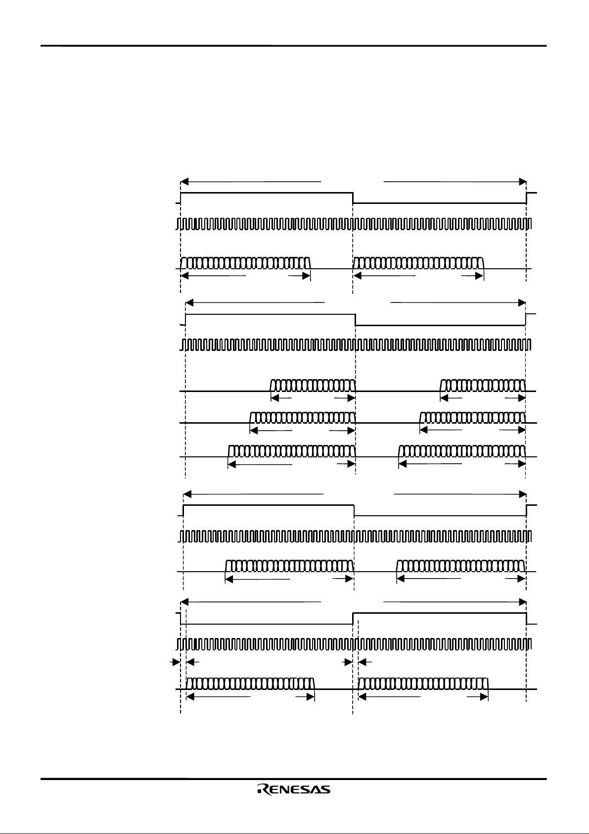
Item Symbol Condition Min.
Typ. Max.
Unit
XfsoIN Duty Ratio duty(XfsoIN) 40 50 60 %
duty(XfsiIN)XfsiIN Duty Ratio
512fsi 30 50 70 %
256fsi 40 50 60 %
SCSHIFT Pulse time tw (SCSHIFT) 160 nsec
SCDT Setup time tsu (SCDT) 80 nsec
SCDT Hold time th (SCDT) 80 nsec
SCLATCH Pulse Width tw (SCLATCH) 160 nsec
SCLATCH Setup Time tsu (SCLATCH) 160 nsec
SCLATCH Hold time th (SCLATCH) 160 nsec
BCK Pulse Width tw (BCK) 35 nsec
DATA Setup Time tsu (DATA) 20 nsec
DATA Hold time th (DATA) 20 nsec
LRCK Setup time tsu (LRCK) 20 nsec
LRCK Hold time th (LRCK) 20 nsec
AC CHARACTERISTICS TIMING CHART
(1)XfsoIN, XfsiIN Duty Ratio
twhl
twh
twl
duty (XfsoIN, XfiIN) =
twh
twhl
(2)SCSHIFT, SCDT, SCLATCH Input Timing
tw (SCSHIFT) tw (SCSHIFT)
SCSHIFT
tsu (SCDT)
SCDT
SCLATCH
(3)BCK, DATA, LRCK Input Timing
tw (BCK)
BCK
DATA
LRCK
th (SCDT)
tw (BCK)
tsu (DATA)
th (DATA)
th (LRCK)
th (SCLATCH)
tw (SCLATCH)
tsu (SCLATCH)
tsu (LRCK)
Rev.1.00 2003.05.08
page 20 of 23
Page 21

M65881AFP
APPLICATION EXAMPLE
DSP
MCU
Initialize Control
Mute Control
Input Mode Select1
Input Mode Select2
LRCK
BCK
DATA
XfsiIN
(Primary Clock)
SCDT
SCSHIFT
SCLATCH
M65881AFP
INIT
NSPMUTE
MODE1
MODE2
T
E
S
T
1
MCKSEL
XFSOIN
(Secondary Clock)
XFSOOUT
FsoCKO
FsoI
OUTL1
OUTL2
OUTR1
OUTR2
HPOUTL1
HPOUTL2
T
E
S
T
2
S
F
L
A
G
HPOUTR1
HPOUTR2
Secondary Clock Select
L:1024Fso H:512Fso
Oscillator
Secondary Clock output
Secondary synchronized clock (For Multi channel )
Power
Driver
Power
Driver
Low Pass Filter
/Headphone Amplifier
Flag Output
Rev.1.00 2003.05.08
page 21 of 23
Page 22

M65881AFP
DETAILED DIAGRAM OF PACKAGE OUTLINE
.42
.40
.20
.717
.68
.2312
–
–
.70
–
–
.150
–
0.9
–
–
I2
.02
.30
.150
.517
.48
.80
.9311
.50
.7651
–
–
0.75
–
–
.4311
–
b2
e
–
Min Nom Max
Dimension in Millimeters
Recommended Mount Pad
e1
A
.250
.050
A1
.130
.317
.28
.6311
.30
–
–
2
c
b
A
–
E
e
E
D
L
H
–
–
1
L
–
0° –10°
z
y
Z1
.271
–
–.50–
2
I2
e1
b
Symbol
F
A1
L
c
A
2
A
L1
Detail F
Lead Material
Cu Alloy+42 Alloy
Weight(g)
––
JEDEC Code
MMP
42 22
EIAJ Package Code
SSOP42-P-450-0.80
42P2R-E Plastic 42pin 450mil SSOP
21
b
y
D
Detail G
z
e
1
Z1
E
G
HE
Rev.1.00 2003.05.08
page 22 of 23
Page 23

M65881AFP
Sales Strategic Planning Div. Nippon Bldg., 2-6-2, Ohte-machi, Chiyoda-ku, Tokyo 100-0004, Japan
Keep safety first in your circuit designs!
1. Renesas Technology Corporation puts the maximum effort into making semiconductor products better and more reliable, but there is always the possibility that trouble may
occur with them. Trouble with semiconductors may lead to personal injury, fire or property damage.
Remember to give due consideration to safety when making your circuit designs, with appropriate measures such as (i) placement of substitutive, auxiliary circuits, (ii) use of
nonflammable material or (iii) prevention against any malfunction or mishap.
Notes regarding these materials
1. These materials are intended as a reference to assist our customers in the selection of the Renesas Technology Corporation product best suited to the customer’s
application; they do not convey any license under any intellectual property rights, or any other rights, belonging to Renesas Technology Corporation or a third party.
2. Renesas Technology Corporation assumes no responsibility for any damage, or infringement of any third-party’s rights, originating in the use of any product data, diagrams,
charts, programs, algorithms, or circuit application examples contained in these materials.
3. All information contained in these materials, including product data, diagrams, charts, programs and algorithms represents information on products at the time of publication
of these materials, and are subject to change by Renesas Technology Corporation without notice due to product improvements or other reasons. It is therefore
recommended that customers contact Renesas Technology Corporation or an authorized Renesas Technology Corporation product distributor for the latest product
information before purchasing a product listed herein.
The information described here may contain technical inaccuracies or typographical errors.
Renesas Technology Corporation assumes no responsibility for any damage, liability, or other loss rising from these inaccuracies or errors.
Please also pay attention to information published by Renesas Technology Corporation by various means, including the Renesas Technology Corporation Semiconductor
home page (http://www.renesas.com).
4. When using any or all of the information contained in these materials, including product data, diagrams, charts, programs, and algorithms, please be sure to evaluate all
information as a total system before making a final decision on the applicability of the information and products. Renesas Technology Corporation assumes no responsibility
for any damage, liability or other loss resulting from the information contained herein.
5. Renesas Technology Corporation semiconductors are not designed or manufactured for use in a device or system that is used under circumstances in which human life is
potentially at stake. Please contact Renesas Technology Corporation or an authorized Renesas Technology Corporation product distributor when considering the use of a
product contained herein for any specific purposes, such as apparatus or systems for transportation, vehicular, medical, aerospace, nuclear, or undersea repeater use.
6. The prior written approval of Renesas Technology Corporation is necessary to reprint or reproduce in whole or in part these materials.
7. If these products or technologies are subject to the Japanese export control restrictions, they must be exported under a license from the Japanese government and cannot
be imported into a country other than the approved destination.
Any diversion or reexport contrary to the export control laws and regulations of Japan and/or the country of destination is prohibited.
8. Please contact Renesas Technology Corporation for further details on these materials or the products contained therein.
http://www.renesas.com
Rev.1.00 2003.05.08
Copyright © 2003. Renesas Technology Corporation, All rights reserved. Printed in Japan.
page 23 of 23
 Loading...