

Page 1

お客様各位
資料中の「三菱電機」、「三菱XX」等名称の株式会社ルネサステクノロジへの変更について
2003年4月1日を以って株式会社日立製作所及び三菱電機株式会社のマイコン、ロジック、
アナログ、ディスクリート半導体、及びDRAMを除くメモリ(フラッシュメモリ・SRAM等)を含
む半導体事業は株式会社ルネサステクノロジに承継されました。
従いまして、本資料中には「三菱電機」、「三菱電機株式会社」、「三菱半導体」、「三菱XX」といっ
た表記が残っておりますが、これらの表記は全て「株式会社ルネサス テクノロジ」に変更され
ておりますのでご理解の程お願い致します。尚、会社商標・ロゴ・コーポレートステートメント
以外の内容については一切変更しておりませんので資料としての内容更新ではありません。
注:「高周波・光素子事業、パワーデバイス事業については三菱電機にて引き続き事業運営を
行います。」
2003年4月1日
株式会社ルネサステクノロジ
カスタマサポート部
Page 2
Mitsubishi Semiconductor
<
Digital IC
>
Digital Video/Chroma/Deflection
+
MCU
Preliminary
Some of information in this document are subject to changes.
TSC TV with a closed caption
Note : This is not a final specification.
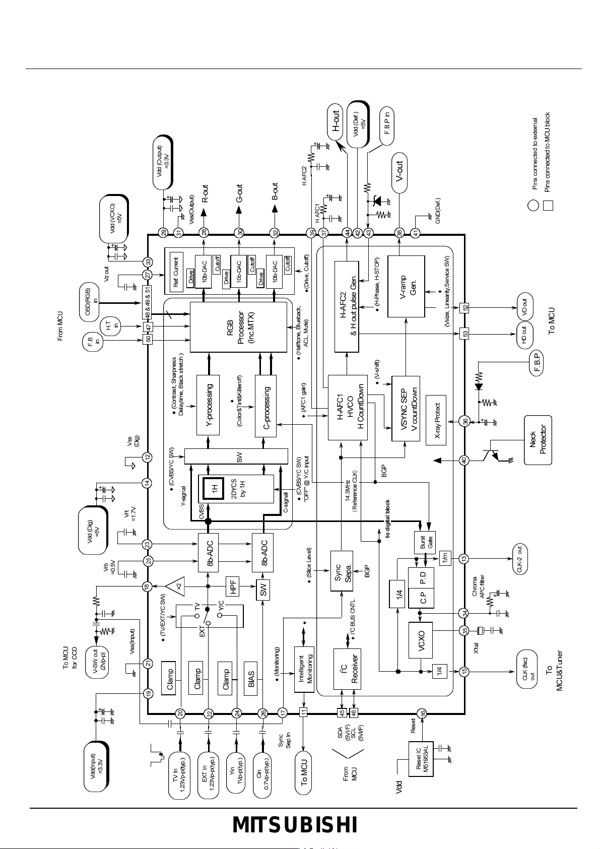
Description
The M65580MAP-XXXFP are semiconductor integrated circuits designed with CMOS silicon gate technology for NTSC television
system, include 8bit MCU( M37272MA core) with a closed caption decoder and circuits needed for TV baseband signals(Video and
Chroma) processor and Deflection in a chip. PCB area and EMI noise can be reduced by one chip and 80QFP, and internal
connection of OSD signals. And it can realize a adjustment free system by built-in MCU and get a high performance adaptive YC
separation by 1 line memory. The above technology makes its performance more stable and better.
Feature
• Y/C processor : 8bit Input, 10bit Output digital processing
• Deflection processor : optimized system by conventional analog and digital mixed solution
• ADC&DAC : 8bit high speed video ADC & 10bit high speed video DAC
[MCU Block]
MCU(single microcomputer) in this IC has almost same function and performance as M37272MA-XXXSP/FP in mass-production.
And it is operated by simple instruction in the same memory space as that of built-in ROM, RAM, I/O.
It has a OSD, data slicer , and I
decoder.
[ASIC Block]
ASIC block consists of the following blocks.
(1) Analog frontend block ; Analog SW(2 CVBS(TV&EXT) inputs, Y/C signals to one signal, 2 channels 8 bit high speed video ADCs,
and ACC amplifiers
(2) Video and Chroma block ; A high performance 2 line adaptive YC separation by 1 line memory, Video blocks including sharpness,
YNR, a high performance blackstretch circuits, Chroma decoder, and RGB matrix including OSD mixing circuit.
(3) Deflection block ; A high performance sync separation by analog and digital mixed solution
(4) Analog backend block ; 3 channels 10 bit high speed video DACs for Cutoff & Drive, and Mute circuit.
2
C-BUS interface. So it is very useful for a channel selection system for N
M65580MAP-XXXFP
Application
NTSC TV with a closed caption decoder
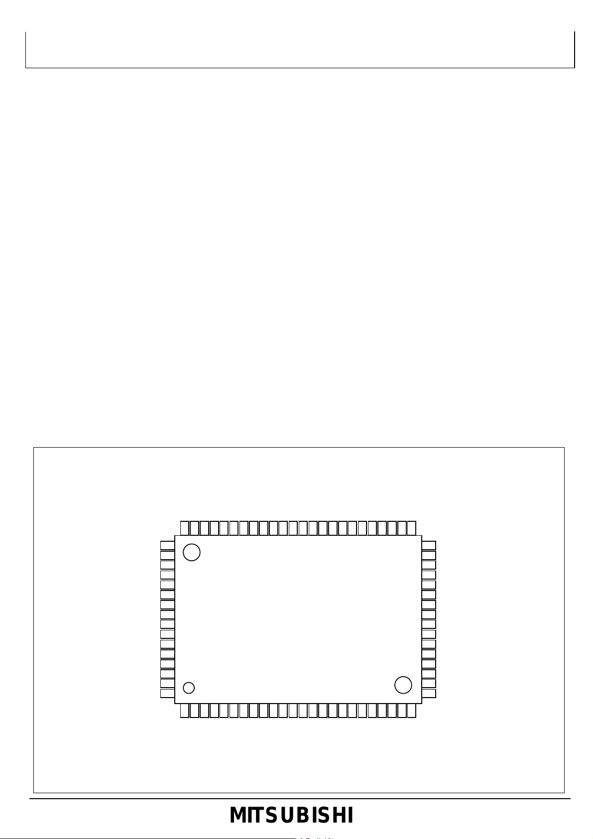
PIN CONFIGURATION (TOP VIEW)
P00/PWM0
P13/SDA1
P14/SDA2
64
62
63
HLF
CV IN
X IN
65
66
67
68
69
70
71
72
73
74
75
76
77
78
79
80
1
3
2
P01/PWM1
P02/PWM2
P03/PWM3
P04/PWM4
P05/AD3
P06/INT2/AD4
P07/INT1
P23/TIM3
P24/TIM2
P25/AD5
VHOLD
CN VSS
X OUT
P12/SCL2
59
60
61
55
56
57
58
53
54
OSD(R) IN
V-PULSE OUT
51
52
P50/HSYNC IN/OUT
P51/VSYNC
P52/R
P53/OUT1
P30/G
P31/B
P10/OUT2
P11/SCL1
M65580MAP-XXXFP
9
8
7
6
5
4
12
11
10
14
13
OSD(B) IN
OSD(G) IN
FAST BLK
48
49
50
17
16
15
SCL
HALF TONE
H OUT
SDA
46
47
44
45
19
18
21
20
VDD(DEF)
FBP IN
42
43
23
22
VSS(DEF)
41
40
NECK PROTECTOR
39
HVCO F/B
38
V-RAMP OUT
37
AFC1 FILTER
36
X-RAY PROTECT
35
X-TAL
34
CHROMA APC FILTER
33
VDD(VCXO)
32
B OUT
31
VSS(OUTPUT)
30
G OUT
29
VDD(OUTPUT)
28
R OUT
27
VZ OUT
26
TV IN
25
VRB
24
VSS
FILT
VCC
P27/XCOUT
RESETB
P22/SIN/AD8
P20/SCLK/AD6
P21/SOUT/AD7
P26/FSCIN/XCIN
P16/AD2/TIM2
P15/AD1/INT3/FSCIN
CLK OUT
OSD CLK
VSS(DIGITAL)
VDD(DIGITAL)
RESETB(ASIC)
MITSUBISHI
EXT IN
Y SW OUT
VDD(INPUT)
SYNC SEP IN
Y IN
C IN
VRT
VSS(INPUT)
1
Page 3
Mitsubishi Semiconductor
<
Digital IC
>
Digital Video/Chroma/Deflection
+
MCU
Preliminary
Some of information in this document are subject to changes.
Note : This is not a final specification.
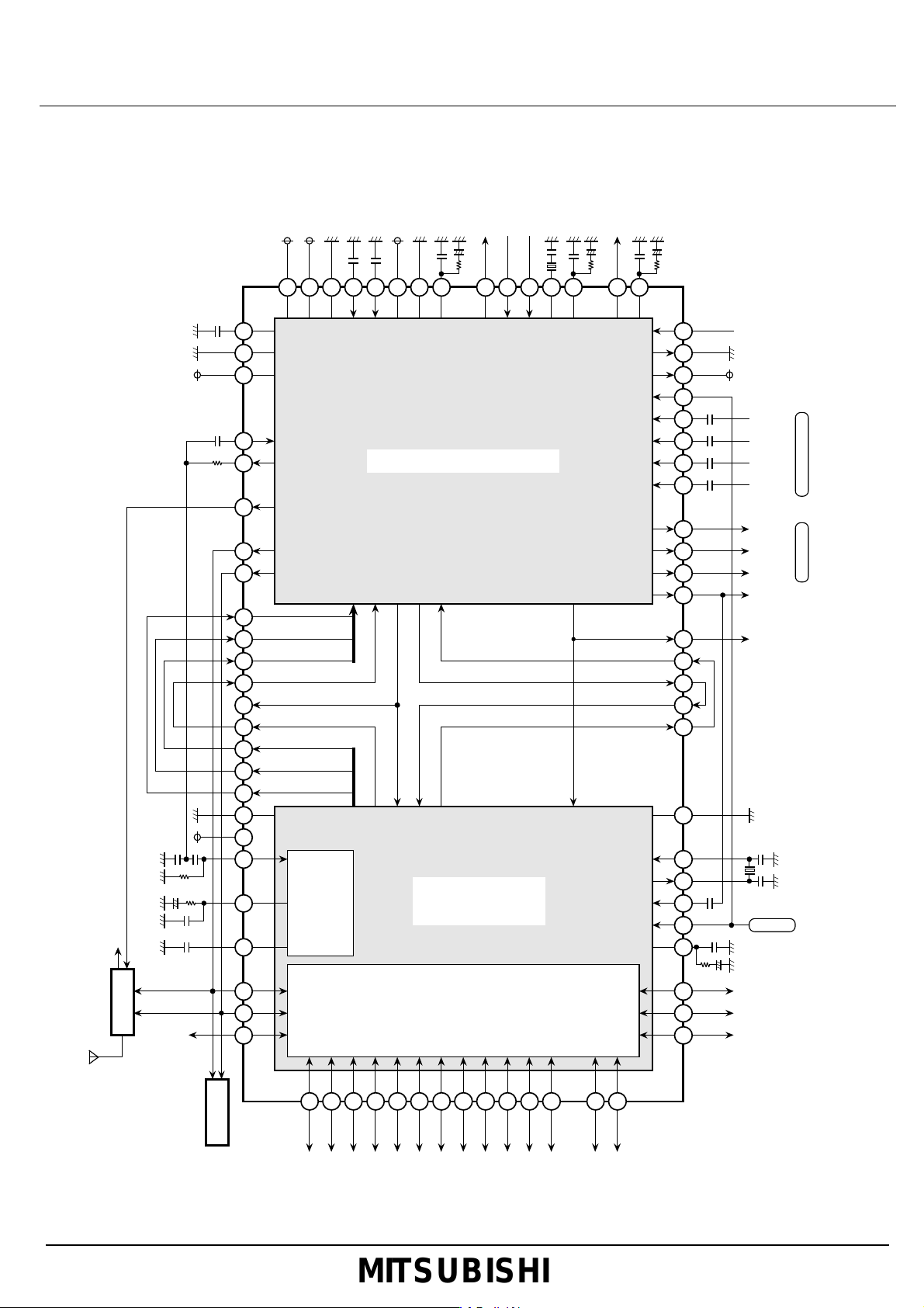
Block Diagram(Whole)
Vss(Input)
Vdd(Input)
Vdd(VCXO)
19 21 25 23 42 41 37 44 43 40 35 34 38 3933
Vrb
Vrt
Vss(DEF)
Vdd(DEF)
AFC1 Filter
H OUT
Neck Protector
FBP IN
Chroma APC Filter
XTAL
M65580MAP-XXXFP
V-RAMP OUT
HVCO F/B
VZ OUT
Vss(OUTPUT)
Vdd(OUTPUT)
Vcc 3
To TV IN of ASIC
27
31
29
1713SYNC SEP IN
18 Y SW OUT
CLK-2 OUT
46
SCL
45 SDA
OSD(B) IN
48
OSD(G) IN
49
OSD(R) IN
51
FAST BLK
50
OSD H-SYNC
53
FAST BLK
56
OSD(R) OUT
58
OSD(G) OUT
57
OSD(B) OUT
55
1Vss
77
75
CV IN
HLF
CCD
76
VHOLD
SIGNAL PROCESSOR
3bit Digital OSD
FAST BLK
OSD
FAST BLK
HD
HD
HALF TONE
VD
VD
HALF TONE
MCU CORE
M37272MA
Intelligent Monitor
HALF TONE
OSD V-SYNC
OSD V-SYNC
HALF TONE
36
12
14
16
26
24
22
20
32
30
28
15
11
59
52
54
47
78 CNVss
79
80
5
6
2 FILT
FSC IN
RESET
X-ray Protect
Vss(Digital)
Vdd(Digital)
RESET
TV IN
C IN
Y IN
EXT IN
B OUT
G OUT
R OUT
CLK(fsc) OUT
INTELLIGENT
MONITOR
RESET
CVBS/YC input
RGB OUT
X IN
X OUT
SCL
SDA
2in1 Tuner
P12/SCL2
60
62
61
EEPROM
63 64 65 66 67 68 69 71 72 73 74 4 770
P14/SDA2
P00/PWM0
I/O PORT
P05/AD3
P07/INT1
P24/TIM2
P02/PWM2
P01/PWM1
P04/PWM4
P03/PWM3
P23/TIM3
P06/INT2/AD4
MITSUBISHI
P25/AD5
P27/XCOUT
P22/S IN/AD8
10
9
8
P15/AD1/INT3
P20/SCLK/AD6
P21/S OUT/AD7
2
Page 4
Mitsubishi Semiconductor
<
Digital IC
>
Digital Video/Chroma/Deflection
+
MCU
Preliminary
Some of information in this document are subject to changes.
Note : This is not a final specification.
Absolute maximum ratings
M65580MAP-XXXFP
Symbol Parameter Ratings Unit
VDD (MCU)
VDD (ASIC5V)
VDD (ASIC3.3V)
VI (MCU)
VO (MCU)
IOH (MCU)
IOL1 (MCU)
IOL2 (MCU)
VID (ASIC)
IOUT (ASIC)
Pd
Kt
Topr
Tstg
Supply voltage (MCU)
Supply voltage (ASIC5V)
Supply voltage (ASIC3.3V)
Input Voltage (MCU)
Output Voltage (MCU)
Circuit current (MCU)
Circuit current (P00-P07, P10, P15,
P16, P20-P27, P30, P31, P52, P53)
Circuit current (P11-P14)
Digital input voltage
Analog output current -30
Power dissipation
Thermal derating
Operating temperature
Storage temperature
All voltage are based on
Vss.Output transistors are
cut off.
Conditions
-0.3 to 6.0
-0.3 to 6.0
-0.3 to 4.0
-0.3 to Vcc+0.3
-0.3 to Vcc+0.3
0 to 1 (See note 1)
0 to 2 (See note 2)
0 to 6 (See note 2)
-0.3 to Vcc+0.3
1460
14.6
-20 to 65
-40 to 125
V
V
V
V
V
mA
mA
mA
V
mA
mW
mW/ ˚C
˚C
˚C
Recommended operating condition
(Ta=-20 to 65 ˚C, unless otherwise noted)
Limits
Symbol Parameter
VDD (MCU)
VDD (Digital)
VDD (Input)
VDD (Output)
VDD (VCXO)
VDD (DEF)
VIH1 (MCU)
VIH2 (MCU)
VIH3 (ASIC)
VIL1 (MCU)
VIL2 (MCU)
VIL3 (MCU) Low Input voltage (See note 4) P50, P51, RESETB,
VIL4 (ASIC) Low Input voltage RESETB, FBP IN, HALF TONE, 0.2Vcc
IOH (MCU)
Supply voltage (MCU) (See note 3)
Supply voltage (Digital) 4.75 5.0 5.25
Supply voltage (Input) 3.13 3.3 3.47
Supply voltage (Output)
Supply voltage (VCXO)
Supply voltage (DEF)
High Input voltage P00-P07, P10-P16, P20-P27, P50,
P51, RESETB, XIN
High Input voltage SCL1, SCL2, SDA1, SDA2
(When using I2C-Bus)
High Input voltage RESETB, FBP IN, HALF TONE,
OSD(R/G/B) IN, FAST BLK
Low Input voltage P00-P07, P10-P16, P20-P27
Low Input voltage SCL1, SCL2, SDA1, SDA2 0.3Vcc
(When using I2C-Bus)
XIN, TIM2, TIM3, INT1, INT2, INT3, SIN, SCLK
OSD(R/G/B) IN, FAST BLK
High average output current (See note 1)
P10-P16, P20-P27, P30, P31, P52, P53
Min. Typ. Max.
4.75 5.0 5.25 V
3.13 3.3 3.47
4.75 5.0 5.25
4.75 5.0 5.25
0.8Vcc
0.7Vcc
0.8Vcc
0
0
0
0
Vcc
Vcc
Vcc
0.4Vcc
0.2Vcc
1
Unit
V
V
V
V
V
V
V
V
V
V
V
V
mA
3
MITSUBISHI
Page 5
Mitsubishi Semiconductor
<
Digital IC
>
Digital Video/Chroma/Deflection
+
MCU
Preliminary
Some of information in this document are subject to changes.
Note : This is not a final specification.
Limits
Symbol Parameter
IOL1 (MCU) 2
Low average output current (See note 2)
P00-P07, P10, P15, P16, P20-P27, P30, P31, P52, P53
Min. Typ. Max.
M65580MAP-XXXFP
Unit
mA
IOL2 (MCU) Low average output current (See note 2) P11-P14 6
f(XIN) (MCU)
fhs1 (MCU)
fhs2 (MCU) Input frequency SCLK MHz1
VI (MCU) Input amplitude video signal CVIN
Note
1: The total current that flows out the MCU must be 20mA or less.
2: The total input current to MCU (IOL1+IOL2) must be 30mA or less.
3: Use a quartz-crystal oscillator or a ceramic resonator for the CPU oscillation circuit. When using the data
slicer, use 8MHz.
4: Pin name in each parameter is described pin names.
(1) Dedicated pins: dedicated pin name.
(2) Double-/Triple-function ports.
When the same limits: I/O port name.
When the limits of function except ports are different from I/O port limits; function pin name.
5: P06, P07, P15, P23, P24 have the hysteresis when these pins are used as interrupt input pins or timer pins.
P11-P14 have the hysteresis when these pins are used as multi-master I2C-Bus interface ports.
P20-P22 have the hysteresis when these pins are used as serial I/O pins.
Oscillation frequency (for CPU operation) XIN 7.9 8.0 8.1
(See note 5)
Input frequency TIM2, TIM3, INT1, INT2, INT3 100 kHz
Input frequency SCL1, SCL2 kHzfhs3 (MCU)
1.5
2.0
400
2.5
mA
MHz
kHzOscillation frequency (for sub-clock operation) XCIN 29 32 35f(XCIN) (MCU)
MHzOscillation frequency (for OSD standard clock) FSCIN 3.58FSCIN (MCU)
V
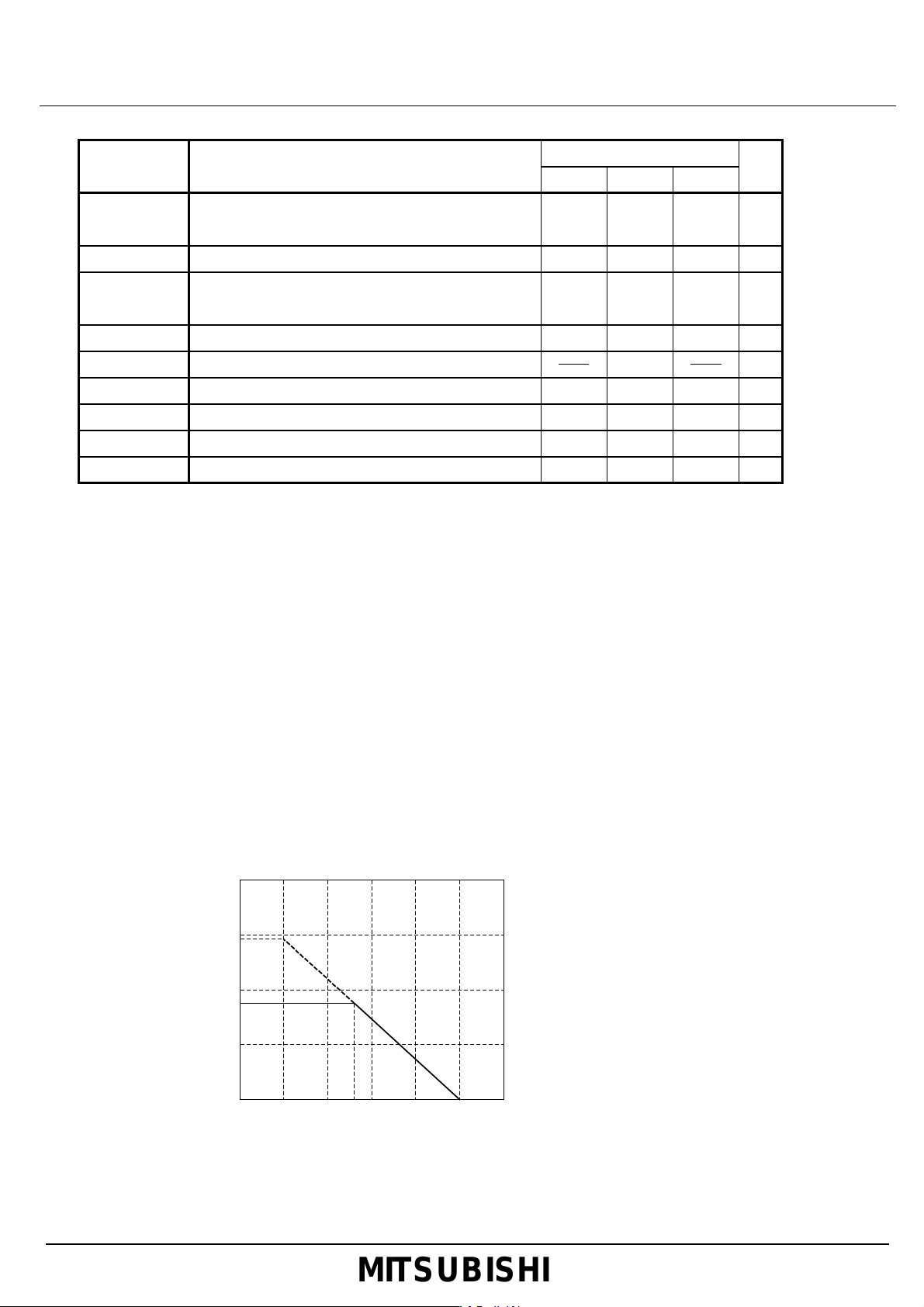
Thermal derating
THERMAL DERATING (MAXIMUM RATING)
2.0
1.5
1.46
1.0
0.88
0.5
POWER DISSIPATION Pd (W)
65 7550250 100 125 150
AMBIENT TEMPERATURE Ta (˚C)
4
MITSUBISHI
Page 6

Mitsubishi Semiconductor
<
Digital IC
>
Digital Video/Chroma/Deflection
+
MCU
Preliminary
Some of information in this document are subject to changes.
Note : This is not a final specification.
[MCU Block(M37272MA)]
Description
MCU(single microcomputers) in this IC has almost same function and performance as M37272MA-XXXSP/FP in massproduction. And it is operated by simple instruction in the same memory space as that of built-in ROM, RAM, I/O.
It has a OSD, data slicer , and I
closed caption decoder.
2
C-BUS interface, so it is very useful for a channel selection system for NTSC TV with a
Features
• Number of basic instructions -------- 71
• Memory size
ROM -------- 40Kbytes
RAM -------- 1152bytes
(ROM correction memory:64bytes included)
• minimum instruction execution time --------- 0.5µs
(at 8 MHz oscillation frequency)
• Power source voltage -------- 5V±10%
• Subroutine nesting -------- 128 levels(max.)
• Interrupts -------- 17bytes 16vector
• 8-bit timers -------- 6
• Programmable I/O ports(Ports P0,P1,P2) -------- 23
• Input ports(Ports P50,P51) -------- 2
• Output ports(Ports P30,P31,P52,P53) -------- 4
• Serial I/O -------- 8-bit x 1channel
• Multi-master I
• A-D comparator (7-bit resolution) -------- 8 channels
• PWM output circuit -------- 8-bit x 5
• ROM correction function -------- 32 bytes x 2
Power dissipation -------- 165mW
(at Vcc=5.5V, 8MHz oscillation frequency, OSD on, and Data slicer on)
• Closed caption data slicer
• OSD function
Display characters -------- 32 characters x 2 lines(possible to display 3 lines or more by software)
Kinds of characters 254 kinds
Character display area CC mode : 16x26 dots
OSD mode : 16x20 dots
Kinds of character sizes CC mode : 1 kind
OSD mode : 8 kinds
Kinds of character colors 8 colors(R,G,B) (coloring unit: a character)
Kinds of background colors CC mode : 1 kind(black)
OSD mode : 8 kinds(possible to select color in character unit)
Display position horizontal : 128 levels Vertical : 512 levels
Attribute CC mode : smooth italic, underline, flash, automatic solid space
OSD mode : border(black)
Kinds of raster colors 8 kinds
Smooth roll-up
Window function
2
C-BUS interface -------- 1(2 systems)
M65580MAP-XXXFP
5
MITSUBISHI
Page 7

Mitsubishi Semiconductor
<
Digital IC
>
Digital Video/Chroma/Deflection
+
MCU
Preliminary
Some of information in this document are subject to changes.
(1) Analog frontend block ; Analog SW(2 CVBS(TV&EXT) inputs, Y/C signals to one signal), 2 channels 8 bit high speed video
• Deflection Block : H-Phase, V-size,
V
-shift, V-Linearity
Note : This is not a final specification.
[ASIC Block]
Description
CVBS(TV/EXT) signals or Y/C signals input to this IC are converted to 8 bit digital signal by 2 channels high speed video
ADCs. These signals are input to digital section to obtain high performance R/G/B signals. First, CVBS signals are separated
to high quality Y/C signals by 2 dimensional adaptive YC separation circuit, and then Y/C signals are converted to R-Y&B-Y
signals by digital chroma decoder, after that, to R/G/B signals by RGB matrix circuit. These signals are mixed with OSD
signals come from MCU block, are converted to analog R/G/B signals by 3 channel 10 bit high speed video DACs. In
deflection block, to get a better Horizontal & Vertical signals, a conventional analog solution by analog CMOS technology is
used.
ASIC block consists of the followings blocks.
ADCs , and ACC amplifiers
(2) Video and Chroma block ; A high performance 2 line adaptive YC separation by 1 line memory, Video blocks including
sharpness, YNR, a high performance blackstretch circuits, Chroma decoder, and RGB matrix including OSD mixing circuit.
(3) Deflection block ; A high performance sync separation by analog and digital mixed solution
(4) Analog backend block ; 3 channels 10 bit high speed video DACs for Cutoff & Drive, and Mute circuit.
Features
[Video/Chroma Block]
• Built-in 1 Video SW for TV/EXT signal input
• 2 additional pins for S(Y/C) input
• YUV input signal available ( T.B.D )
• 2 channel 8 bit Video ADCs for CVBS(TV&EXT) or Y/C signal inputs
• Built-in adaptive 2 line comb filter(2DYCS) => Few dot crawl&crosscolor, and clear color transition
• Built-in a high performance Blackstretch => Dynamic & detailed picture
• Digital Luminance delay circuit => stable Y/C timing adjustment
• Built-in VCXO circuit(4fsc)
• High resolution R/G/B output => Built-in 10bit high speed Video DACs
• Internal connection of 8 color digital OSD ( R/G/B, F.B, H.T )
• Reference CLK output for tuner (fsc or 4MHz)
• Built-in YNR ( about fsc±1MHz)
• Gamma correction(for R/G/B signals)
M65580MAP-XXXFP
[Deflection Block]
• Analog(conventional) sync separation => Better performance by abundant experience
• Double AFC Circuit => Stable Horizontal scanning
• Built-in Horizontal reference Oscillator => No ceramic resonator and Adjustment free
• HD and VD pulse by Countdown => Stable HD&VD
• Built-in digital Vramp generator
[List of main I
• Chip : Power-down mode
• Analog Input Stage : CVBS/Y&C Input SW
• Luminance Processing : Sharpness, Blackstretch
• Chroma Processing : Color, Tint, Killer level
• RGB Matrix : ACL, OSD Input Level, Contrast, Brightness
• Analog Output Stage : Drive adj.(R/G/B), Cutoff adj.(R/G/B)
2
C bus controllable Items]
MITSUBISHI
6
Page 8
Mitsubishi Semiconductor
<
Digital IC
>
Digital Video/Chroma/Deflection
+
MCU
Preliminary
Some of information in this document are subject to changes.
Note : This is not a final specification.
ASIC Block Detailed Diagram
M65580MAP-XXXFP
7
MITSUBISHI
Page 9

Mitsubishi Semiconductor
<
Digital IC
>
Digital Video/Chroma/Deflection
+
MCU
Preliminary
Some of information in this document are subject to changes.
Linearity : 0 to 30 % by 7bit
Note : This is not a final specification.
Function and Outline of ASIC Block
Chip
Power down mode : 3 modes [ PD0 & PD1 & PD2 ]
Service SW : stop of Vertical(Vramp) output ( For cutoff adjustment )
Analog Block
• Input stage => CVBS&Y/C input signals
Input level (CVBS) : 1.23Vp-p (173IRE) @max. / 1.0Vp-p @typ.
Input level (Y/C) : Y:1.00Vp-p (140IRE) @typ./ C:0.7Vp-p @typ.
• Output stage => RGB output signals
Output level : 0.7 Vp-p (typ.)
Drive(R&G&B) : -3 to +4 dB by 7bit (White Balance)
Cutoff(R&G&B) : 0.5 V by 9bit (Start lighting point)
Digital Block
• 2DYCS
Adaptive YC separation by using of 1H line memory and original algorithm
• Luminance processing
Contrast : 0 to 200 LSB by 7bit
Brightness : -20 to 20 LSB by 8bit (Pedestal DC level)
Sharpness : 0 to 3 dB by 5bit (by 0, 70, 140, 210ns)
Delay adjustment : 0 to 210 ns by 2bit(70ns step) to Chroma signal
Blackstretch : 3 selectable stretch point
[ Stretch areas ( 0 to 25/30/40IRE ), Through areas ( 25/30/40IRE ~ ) ]
4 selectable blackstretch curves ( 1/4, 2/4, 3/4, 4/4)
• Chroma processing
Tint : -45 to 45 degree by 7bit => about 0.7 degree
: Variable demodulator (R-Y) axis
(-22.5 to +22.5 degree by 6bit => about 0.7 degree)
Color : 0 to 200 % by 7bit
M65580MAP-XXXFP
• RGB matrix
: Matrix(R-Y signal) ratio selectable (12/8, 13/8, 14/8)
ACL : Automatic Contrast Limiter by MCU port(ADC) and I
EXT/RGB : clip to 7LSB @ data < 0Fh
BlueBack : ON/OFF selectable
Mute : ON/OFF of R/G/B output
Neck Protector : R/G/B output to zero( no signal)
Deflection Block
• Horizontal Output
AFC2 phase : +5 to -5µs by 5bit
Hold => Shut down : fh@Hold-down : in about 16.5KHz => fh@Shutdown : H-STOP
AFC1 gain : Normal/High selectable for VTR skew
• Vertical Output
V position : 0 to 16 H by 3 bit => 2H unit(connected with BLK)
V size : 1.4 to 2.6 V by 7bit
2
C bus
MITSUBISHI
8
Page 10
Mitsubishi Semiconductor
<
Digital IC
>
Digital Video/Chroma/Deflection
+
MCU
Preliminary
Some of information in this document are subject to changes.
0.1u
0.1u
0.1u
0.1u
0.1u
1M
560
0.1u
2K
+200V
0.1u
0.1u
10K
10K
510157480
1211131476777879234
678919
18171612024232221656965666768707172736425
29
282726
30
35363433323140
3938373940
45495459535251414243444647485055565758
60616263CLK-2 Out
CLK(fsc) Out
Vdd(Dig)
Vss(Dig)
Sync Sep. In
CVBS(x2) Out
Vdd(Input)
TV in
Reset In
P22/Sin/AD8
P21/Sout/AD7
P20/SCLK/AD6
P15/AD1/INT3
Reset In
P26/FSCin
P27/Xcout
VCC
Vss(Input)
EXT in
Vrt
Vss
FILT
P16/AD2/TIM2 (Int. Mon. In/Out)
R(OSD) in
F.B in
SDA
SCL
G(OSD) in
B(OSD) in
P51/Vsync
Vdd(Def)
Vss(Def.)
P52/Rout
P53/OUT1
P30/Gout
P31/Bout
VD out
P10/OUT2
P11/SCL1
P12/SCL2
P13/SDA1
P14/SDA2
H.T in
P50/Hsync In/out
H OUT
P00/PWM0
Yin
FBP IN
NECK PRO65647475
5V5V3.3V
5V
3.3V
5V
9V
3.3V
5V
15p
15p
470p
0.1u
0.1u
470p
0.01u
470p
0.1u
0.01u
Note : This is not a final specification.
Application Examples
M65580MAP-XXXFP
SW REG
REG
ACL In
FBT
SDA
Reset
SCL
MCU
POWER ON H
Digital Block
REG
REG
Video det out
(1.23Vp-p)
EXT In
(1.23Vp-p)
Y In
(1.00Vp-p)
C In
(0.70Vp-p)
150V
REG
1.5K
1.5K
ASIC
Analog Block
H-Pulse Out
FBP in
-
DY
to H DRIVE
FBT
1.5K
9
MITSUBISHI
Page 11

Mitsubishi Semiconductor
<
Digital IC
>
Digital Video/Chroma/Deflection
+
MCU
Preliminary
Some of information in this document are subject to changes.
Note : This is not a final specification.
Electrical characteristics
Symbol Parameter
ICC Standard conditions
Input signal
Pins SG
Test
point
Min.
Limits
M65580MAP-XXXFP
(Ta=25ºC, Vdd=5.0V, 3.3V)
Unit
Max.Typ.
Remarks
ICC50 5.0V supply current - -
ICC33 3.3V supply current - - 18, 29 47 56 65 mA Supply of A/D and D/A
VIDEO
2AGTV
2AGEV
Vtyp Video standard output 26 SG.A
FBY
Y/C1 Y/C separation function 1 26 SG.E
Y/C2 Y/C separation function 2 26 SG.E
Y/C3 Y/C separation function 3 26 SG.E
YDL0 Y total delay time 26 SG.A
YDL1 Y delay time 1 26 SG.A
YDL2 Y delay time 2 26 SG.A
YDL3 Y delay time 3 26 SG.A
GTnor
GTmax
GTmin
BLS
HT Half Tone function 26 SG.A
Standard conditions of
video character
Video SW output level (TV
input)
Video SW output level
(External input)
Video frequency
characteristics
Video tone control
characteristic 1
Video tone control
characteristic 2
Video tone control
characteristic 3
Black stretch
characteristic
- - - - - - -
26 SG.A 18 1.5 1.7 1.9 Vpp
20 SG.A 18 1.5 1.7 1.9 Vpp
26 SG.B
26 SG.B
26 SG.B
26 SG.B
26 SG.D
3,14,
33,42
28,30,
32
28,30,
32
28,30,
32
28,30,
32
28,30,
32
28,30,
32
28,30,
32
28,30,
32
28,30,
32
28,30,
32
28,30,
32
28,30,
32
28,30,
32
28,30,
32
102 116 130 mA
590 740 890 mVpp
-3 0 3 dB f=5MHz
- -30 -20 dB feb=fec=fsc
-3 0 3 dB feb=fsc, fec=fsc±1/2fH
- -30 -20 dB feb=fsc, fec=fsc±fH
2.4 3.0 3.6 µsec
50 70 90 nsec YDL1=measure – YDL0
50 70 90 nsec YDL2=measure – YDL1
50 70 90 nsec YDL3=measure – YDL2
640 800 960 mV f=2.5MHz
1 2.5 4 dB f=2.5MHz
-7 -4 -1 dB f=2.5MHz
20 50 80 mV
-9 -6 -3 dB
Supply of MCU, Digital, VCXO and
Deflection
Vy=0.18V,
45H=80h(BLS ON) / 00h(BLS OFF)
10
MITSUBISHI
Page 12

Mitsubishi Semiconductor
<
Digital IC
>
Digital Video/Chroma/Deflection
+
MCU
Preliminary
Some of information in this document are subject to changes.
Note : This is not a final specification.
M65580MAP-XXXFP
Symbol
CHROMA
CnorR
CnorB
ACC1
ACC2
VikN
KillP
APCU
APCL
DEMR
DEMP
Ccon 1
Ccon 2
TC1
TC2
Parameter
Standard condition of
chroma parameter
Chroma standard output
(R-Y)
Chroma standard output
(B-Y)
ACC characteristic 1 26 SG.E 28 -3 0 3 dB Veb, Vec : +6dB of typical input level
ACC characteristic 2 26 SG.E 28 -3 0 3 dB
Killer operation input level 26 SG.E 28 -40 -35 -30 dB
Color residual at Killer on 26 SG.E 28 - -40 -28 dB
APC pull-in range (upper) 26 SG.E 28
APC pull-in range (lower) 26 SG.E 28 - - -400 Hz
Demodulated output ratio 26 SG.E
Demodulation phase
angle
Color control characteristic
1
Color control characteristic
2
TINT control characteristic
1
TINT control characteristic
2
Input signal
- -
26 SG.E
26 SG.E
26 SG.F
26 SG.E
26 SG.E
26 SG.F
26 SG.F
Test
point
SGPins
- - - -
28 155 180 205
32 275 310 345
28,32 0.47 0.57 0.67
28,32
28
28 - 0
28,32
28,32
Limits
Min. Typ. Max.
400 - -
85 90 95 deg
160
-60 -45 -30 deg
200
30 45 60 deg
Unit Remarks
mV feb=fec+50kHz
mV
Hz
240 %
10 %
- 5DH=03h
feb=fec+50kHz
Veb, Vec : -20dB of typical input level
Veb, Vec : variable
Veb = 0mV
feb=fec : variable
feb=fec : variable
-
feb=fec+50kHz
feb=fec+50kHz
feb=fec+50kHz
Fclk
Vclk
CLK output frequency 26 SG.C 15 3.578 3.579 3.580 MHz
CLK output amplitude 26 SG.C 15 350 500 650 mVpp
11
MITSUBISHI
Page 13

Mitsubishi Semiconductor
<
Digital IC
>
Digital Video/Chroma/Deflection
+
MCU
Preliminary
Some of information in this document are subject to changes.
Note : This is not a final specification.
M65580MAP-XXXFP
Symbol
RGB
VPED Output Pedestal voltage 26 SG.D
MTXRB
MTXGB
GYmax
GYmin
GYEclip
Lum
max
Lum min
D(R)1
D(G)1
D(B)1
D(R)2
D(G)2
D(B)2
C(R)1
C(G)1
C(B)1
C(R)2
C(G)2
C(B)2
Standard condition of
RGB parameter
Matrix ratio R/B
Matrix ratio G/B
Contrast control
characteristic 1
Contrast control
characteristic 2
Contrast control
characteristic 5
Brightness control
characteristic 2
Brightness control
characteristic 3
R Drive control
characteristic 1
G Drive control
characteristic 1
B Drive control
characteristic 1
R Drive control
characteristic 2
G Drive control
characteristic 2
B Drive control
characteristic 2
R Cut off control
characteristic 1
G Cut off control
characteristic 1
B Cut off control
characteristic 1
R Cut off control
characteristic 2
G Cut off control
characteristic 2
B Cut off control
characteristic 2
Parameter RemarksUnit
Input signal
SGPins
- -
26 SG.H
26 SG.H
26 SG.D
26 SG.D
48,49,
SG.G
51
26 SG.D
26 SG.D
26 SG.D 28 1.5 3.5 5.5 dB Vy =0.286V
26 SG.D 30 1.5 3.5 5.5 dB Vy =0.286V
26 SG.D 32 1.5 3.5 5.5 dB Vy =0.286V
26 SG.D 28 -4.6 -2.6 -0.6 dB Vy =0.286V
26 SG.D 30 -4.6 -2.6 -0.6 dB Vy =0.286V
26 SG.D 32 -4.6 -2.6 -0.6 dB Vy =0.286V
26 SG.D 28 210 260 310 mV Vy =0.286V
26 SG.D 30 210 260 310 mV Vy =0.286V
26 SG.D
26 SG.D 28 -310 -260 -210 mV Vy =0.286V
26 SG.D 30 -310 -260 -210 mV Vy =0.286V
26 SG.D
Test
point
- - - -
28,30,
32
28,32 0.74 0.92 1.10 -
30,32 0.24 0.33 0.42 -
28,30,
32
28,30,
32
28,30,
32
28,30,
32
28,30,
32
32
32
-310 -260 -210 mV Vy =0.286V
Limits
Min. Typ. Max.
2.7
160
250 300 350
100 150 200 mV
-200 -150 -100 mV Vy =0.286V
210 260 310 mV Vy =0.286V
3.0 3.3 V Vy = 0.0V
200
- 0
240 % Vy =0.286V
10 % Vy =0.286V
-
mV
OSD(R) OSD (R) output level 51 SG.G 28 500 600 700 mVpp
OSD(G) OSD (G) output level 49 SG.G 30 500 600 700 mVpp
OSD(B) OSD (B) output level 48 SG.G 32 500 600 700 mVpp
SOSD1
SOSD2
OFF(R)
OFF(G)
OFF(B)
NECK
OSD speed characteristic148,49,
OSD speed characteristic248,49,
Offset voltage between R
and OSD(R)
Offset voltage between G
and OSD(G)
Offset voltage between B
and OSD(B)
Neck protector function
threshold voltage
51
51
-
-
-
26 SG.A 40
SG.G
SG.G
28,30,
32
28,30,
32
-
-
-
- 100 200 nsec
- 100 200 nsec
- -50 0 50 mV Difference at pedestal level
- -50 0 50 mV Difference at pedestal level
- -50 0 50 mV Difference at pedestal level
1.0 1.3 1.6 V
while monitoring at pins 28, 30, 32
MITSUBISHI
12
Page 14

Mitsubishi Semiconductor
<
Digital IC
>
Digital Video/Chroma/Deflection
+
MCU
Preliminary
Some of information in this document are subject to changes.
Note : This is not a final specification.
M65580MAP-XXXFP
SG
Test
point
Min.
Limits
Max.Typ.
Symbol Parameter
DEF
fH1
fH2
fH3
FPHU
FPHL
HPV Horizontal pulse amplitude 26 SG.A 44 4.0 4.5 5.0 V
HPTW Horizontal pulse width 26 SG.A 44 19.3 22.3 25.3 µsec
HPD
HPT1 Horizontal pulse timing 1 26 SG.A 44 8.7 10.7 12.7 µsec
HPT2 Horizontal pulse timing 2 26 SG.A 44 2.2 4.2 6.2 µsec
HPT3
HDOWN
SDOWN
fV
Standard condition of
defrection parameter
Horizontal free-running
frequency 1
Horizontal free-running
frequency 2
Horizontal free-running
frequency 3
Horizontal pull-in range
(upper)
Horizontal pull-in range
(lower)
Horizontal pulse duty
cycle
Horizontal pulse timing
variable range
Hold down function
threshold voltage
Shut down function
threshold voltage
Vertical free-running
frequency
Input signal
Pins
- - - - - - -
- - 44 15.53 15.73 15.93 kHz
- - 44 13.72 14.32 14.92 kHz
- - 44 17.25 17.85 18.45 kHz
17 SG.I 44 250 500 - Hz Vary frequency of input signal.
17 SG.I 44 - -500 -250 Hz Vary frequency of input signal.
26 SG.A 44 30 35 40 %
26 SG.A 44 4.5 6.5 8.5 µsec HPT2 – HPT1
26 SG.A 36 3.0 3.1 3.2 V while monitoring at pin 44
26 SG.A 36 3.3 3.5 3.7 V while monitoring at pin 44
- - 38 55 60 65 Hz
RemarksUnit
SVC
FPVU
FPVL
VRsi 1 Vertical ramp size 26 SG.A 38 2.1 2.5 2.9 Vpp
VRsc 1
VRsc 2
VLin 1
VLin 2
VRpo 1
VRpo 2
VW Vertical pulse width 26 SG.A 52 0.35 0.53 0.65 msec
VBLKW Vertical blanking width 26 SG.A
WVSS
Service mode function
Vertical pull-in frequency
(upper)
Vertical pull-in frequency
(lower)
Vertical ramp size control
range 1
Vertical ramp size control
range 2
Vertical ramp Linearity
control range 1
Vertical ramp Linearity
control range 2
Vertical ramp position
control range 1
Vertical ramp position
control range 2
Minimum vertical sync
detection width
- - 38
17 SG.J 38 - - 63 Hz Vary frequency of input signal.
17 SG.J 38 57 - - Hz Vary frequency of input signal.
26 SG.A 38 20 27 35 %
26 SG.A 38 -35 -27 -20 %
26 SG.A 38 -5 0 5 %
26 SG.A 38 19 24 29 %
26 SG.A 38 0 50 200
26 SG.A 38 790 940 1090
28,30,
26 SG.A 11 13 18 23 µsec
2.5 2.8 3.1 V
1.52 1.64 1.76 msec
32
µsec
µsec
(Measured value) – (Vrpo 1)
13
MITSUBISHI
Page 15

Mitsubishi Semiconductor
<
Digital IC
>
Digital Video/Chroma/Deflection
+
MCU
Preliminary
Some of information in this document are subject to changes.
Note : This is not a final specification.
Electrical characteristics (MCU part)
Symbol Parameter
M65580MAP-XXXFP
(Vcc=5V±10%, Vss = 0V, f(XIN)=8MHz, Ta=–20˚C to 65˚C, unless otherwise noted)
Test conditions
VCC = 5.5 V,
f(XIN) = 8 MHz
OSD OFF
Data slicer OFF
OSD ON
Min.
Limits
Typ.
15
30
Max.
30
45
Unit
mA
Test
circuit
ICC
VOH
VOL
VT+ – VT–
IIZH
IIZL
RBS
System operation
Power source current
Wait mode
HIGH output voltage
LOW output voltage
LOW output voltage P1
Hysteresis (See note 1)
RESET, P50–P51, INT1, INT2,
INT3, TIM2, TIM3, SIN, SCLK, SCL1,
SCL2, SDA1, SDA2
HIGH input leak current
P00–P07, P10–P16, P20–P27,
P50, P51, RESET
LOW input leak current
P00–P07, P10–P16, P20–P27,
P50, P51, RESET
2
C-BUS • BUS switch connection resistor
I
(between SCL1 and SCL2, SDA1 and SDA2)
P10–P16, P20–P27,
P30, P31, P52, P53
P00–P07, P10,
P15, P16, P20–P27,
P30, P31, P52, P53
1–P14
VCC = 5.5 V, f(XIN) = 0,
f(XCIN) = 32 kHz,
OSD OFF, Data slicer OFF,
Low-power dissipation mode set
(CM5 = "0", CM6 = "1")
VCC = 5.5 V, f(XIN) = 8 MHz
VCC = 5.5 V, f(XIN) = 0,
f(XCIN) = 32 kHz,
Low-power dissipation mode set
(CM5 = "0", CM6 = "1")
VCC = 5.5 V, f(XIN) = 0,
f(XCIN) = 0
VCC = 4.5 V
IOH = –0.5 mA
VCC = 4.5 V
IOL = 0.5 mA
VCC = 4.5 V
VCC = 5.0 V
VCC = 5.5 V
VI = 5.5 V
VCC = 5.5 V
VI = 0 V
VCC = 4.5 V
IOL = 3 mA
IOL = 6 mA
2.4
60
25
0.5
µA
200
1
2
1
4
100
10
0.4
0.4
0.6
1.3
5
5
130
mA
µA
V
V
V
µA
µA
2
3
4
4
5
Notes 1: P06, P07, P15, P23, P24 have the hysteresis when these pins are used as interrupt input pins or timer input pins. P11–P14 have the hysteresis when these
pins are used as multi-master I2C-BUS interface ports. P20–P22 have the hysteresis when these pins are used as serial I/O pins.
2: Connect 0.1µF or more capacitor externally between the power source pins VCC–VSS so as to reduce power source noise.
Also connect 0.1µF or more capacitor externally between the pins VCC–CNVSS.
3: Use a quartz-crystal oscillator or a ceramic resonator for the CPU oscillation circuit. When using the data slicer, use 8 MHz.
4: Pin names in each parameter is described as bellow.
(1) Dedicated pin: dedicated pin names.
(2) Double-/triple-function ports
• When the same limits: I/O port name.
• When the limits of functions except ports are different from I/O port limits: function pin name.
14
MITSUBISHI
Page 16

Mitsubishi Semiconductor
<
Digital IC
>
Digital Video/Chroma/Deflection
+
MCU
Preliminary
Some of information in this document are subject to changes.
Note : This is not a final specification.
I2C Bus Table
M65580MAP-XXXFP
SLAVE ADDRESS= BAH(WRITE), BBH(READ)
A6 A5 A4 A3 A2 A1 A0 R/W
1 0 1 1 1 0 1 1/0
WRITE TABLE(input bytes)
SUB ADDRESS
HEX BIN D7 D6 D5 D4 D3 D2 D1 D0 INITIAL
00H 00000000 0 0 0 0 0 0 1 0 02H
01H 00000001 0 0 0 0 1 0 0 0 08H
02H 00000010 0 0 0 0 1 0 0 0 08H
04H 00000100 V1 V0 V1 V0 V0 V0 V0 V0 A0H
05H 00000101 V1 V0 V1 V0 V0 V0 V0 V0 A0H
06H 00000110 V0 V0 V0 V0 V0 V0 V0 V0 00H
07H 00000111 V0 V0 V0 V1 V0 V1 V0 V1 15H
08H 00001000 V0 V0 V1 V0 V1 V0 V0 V1 29H
09H 00001001 V0 V0 V1 V0 V1 V0 V0 V0 28H
0AH 00001010 V0 V0 V1 V1 V1 V0 V1 V1 3BH
0BH 00001011 V0 V0 V0 V1 V1 V1 V1 V0 1EH
0CH 00001100 V1 V0 V0 V1 V1 V1 V1 V0 5EH
0DH 00001101 V0 V0 V0 V1 V1 V1 V1 V0 0EH
0EH 00001110 V1 V0 V0 V0 V0 V0 V0 V0 80H
0FH 00001111 0 0 0 0 1 0 0 0 08H
10H 00010000 0 0 0 0 0 0 0 0 00H
11H 00010001 V0 V1 V0 V0 V0 V0 V0 V0 40H
12H 00010010 1 0 0 0 0 0 0 0 80H
13H 00010011 0 0 0 1 0 0 0 0 10H
14H 00010100 0 1 0 0 0 0 0 0 40H
15H 00010101 1 1 1 1 1 1 1 1 FFH
16H 00010110 00H
17H 00010111 00H
18H 00011000 00H
19H 00011001 00H
1AH 00011010 00H
1BH 00011011 00H
1CH 00011100 0 0 0 0 0 0 0 0 00H
1DH 00011101 0 0 0 0 0 0 0 0 00H
51H
01010001 0 0 0 0 0 0 0 0 00H
DATA
Power Down Mode(not asigned)
X-ray Enable YUV input Y/C input EXT input TV input Y/C through
Ped Clamp
Sharpness Delay (Front)
Sharpness Delay (Rear)
(not asigned) YNR SW
(not asigned) Sharpness Limitter Level
(not asigned) Tint Control
(not asigned) Color Control
(not asigned) Contrast Control
Half Tone OSD Level (R)
RGB Matrix Ratio OSD Level (G)
OSD Comp OSD Level (B)
(not asigned) H Free AFC1 Gain
(not asigned)
(not asigned) Black Stre. SW
RGB Mute
Service SW
V-Blanking Stop
V-Ramp Invert
V0 V0 V0 V0 V0 V0 V0 V0
CutOff(R) MSB
V0 V0 V0 V0 V0 V0 V0 V0
V0 V0 V0 V0 V0 V0 V0 V0
CutOff(G) MSB
V0 V0 V0 V0 V0 V0 V0 V0
V0 V0 V0 V0 V0 V0 V0 V0
CutOff(B) MSB
V0 V0 V0 V0 V0 V0 V0 V0
(not asigned) Intelligent Monitor (Digital)
Y DL Time Adj. YNR Limitter Level
Brightness Control
(for evaluation) 2D Y/C
V-Shift
(not asigned) Intelligent Monitor (Analog)
I/M(D) Enable
H VCO Adjust
Shrapness Gain (Front)
Shrapness Gain (Rear)
H Phase Control
(for evaluation)
(for evaluation)
Gamma Control(inhibited)
(inhibited)
V-Ramp Size
V-Ramp Linearity
Cut Off (R)
Drive (R)
Cut Off (G)
Drive (G)
Cut Off (B)
Drive (B)
(for evaluation)
Sync-tip ClampVRT Voltage(not asigned)
Hold Down Level
NOTE: V0 / V1 ==> V- LATCH BIT
H Stop
READ TABLE(output bytes)
SUB ADDRESS
60H 01100000
61H 01100001
62H 01100010
63H 01100011
D7 D6 D5 D4 D3 D2 D1 D0
KILLER
B2 ROM MSB
H COINCI V COINCI
(not asigned) C Gain
B_W
B2 ROM
IIC_STILL
MV_180
(not asigned)BLKDETV
DET NZ K_MONI
15
MITSUBISHI
Page 17

Mitsubishi Semiconductor
<
Digital IC
>
Digital Video/Chroma/Deflection
+
MCU
Preliminary
Some of information in this document are subject to changes.
Note : This is not a final specification.
Bus function
WRITE
FUNCTION BIT
H STOP 1 00H D0
Power Down 2 00H D1-D2
Input Video SW 4 01H D3-D6
X-ray Enable 1 01H D7
Y/C through 1 01H D2
Sync-tip Clamp 3 02H D0-D2
Ped Clamp 1 02H D7
VRT Voltage 2 02H D3-D4
Sharpness Gain (Front) 6 04H D0-D5
Sharpness Delay (Front) 2 04H D6-D7 Over-shoot width control (0: 0ns, 1: 70ns, 2: 140ns 3: 210ns) 10 V Latch
Sharpness Gain (Rear) 6 05H D0-D5
Sharpness Delay (Rear) 2 05H D6-D7 Pre-shoot width control (0: 0ns, 1: 70ns, 2: 140ns 3: 210ns) 10 V Latch
YNR SW 7 06H D4 YNR control switch (0: YNR OFF, 1: YNR ON) 0
YNR Limiter Level 1 06H D0-D3
Y DL Time Adj. 2 06H D5-D6
Sharpness Limiter Level 6 07H D0-D5
Tint Control 7 08H D0-D6 Tint Control by 7bit 0101001
Color Control 7 09H D0-D6 Color Saturation control by 7bit 0101000
Contrast Control 7 0AH D0-D6 Contrast control by 7bit 0111011
OSD Level (R)
Half Tone
OSD Level (G)
RGB Matrix Ratio 2 0CH D6-D7
OSD Level (B)
OSD Comp 2 0DH D6-D7
Brightness Control 8 0EH D0-D7 Brightness control by 8bit 10000000
AFC2 H Phase 5 0FH D0-D4
AFC1 Gain 1 0FH D5 Horizontal AFC gain switch (0: Low, 1: High) 0
H-free 1 0FH D6 Horizontal forced free-running mode switch (0: OFF, 1: Forced Free-running) 0
2D Y/C 1 10H D4
Black Stretch SW 1 11H D6
Gamma Control 1 12H D0-D3 RGB gamma threshold control (0:Gamma OFF) 0000
RGB Mute 1 12H D7 RGB signal mute ON/OFF switch (0: Mute 1: RGB output) 1
Hold Down Level 3 13H D0-D2 Hold Down level adjustment by 3bit 000
V Shift 3 13H D4-D6
Service SW 1 13H D3
V-Ramp Size 7 14H D0-D6 V-Ramp amplitude adjustment by 7bit 1000000
Test 1 14H D7 No use for customer (Test mode) 0
V-Ramp Linearity 7 15H D0-D6 V-Ramp linearity adjustment by 7bit 1111111
V-Ramp Invert 1 15H D7 V-Ramp polarity switch 1
Cut Off(R) 9 16H D0-D7 R OUT pedestal level adjustment by 9bit
Drive(R) 7 17H D0-D6 R OUT amplitude adjustment by 7bit 0000000
Cut Off(G) 9 18H D0-D7 G OUT pedestal level adjustment by 9bit 00000000
Drive(G) 7 19H D0-D6 G OUT amplitude adjustment by 7bit 0000000
Cut Off(B) 9 1AH D0-D7 B OUT pedestal level adjustment by 9bit 00000000
Drive(B) 7 1BH D0-D6 B OUT amplitude adjustment by 7bit 0000000
Intelligent Monitor (Analog) 4 1CH D0-D3 Intelligent Monitor (Analog) mode selector 0000
Intelligent Monitor (Digital) 5 1DH D0-D4 Intelligent Monitor (Digital) mode selector 00000
Intelligent Monitor(D) Enable 1 1DH D5
H VCO Adj.
SUB
DATA
ADD
6 0BH D0-D5
2 0BH D6-D7 Setting of Half Tone mode 00
6 0CH D0-D5
6 0DH D0-D5
17H D7 0
19H D7 0
1BH D7 0
8 51H D0-D7
Horizontal output switch (0: H OUT, 1: H STOP)
Power down mode control (0: normal, 1: PD0, 2: PD1, 3: PD2)
Video SW Selector (1: TV, 2: EXT, 4: Y/C input, 9: YUV input)
X-ray protect function switch (0: X-ray Protect OFF, 1: X-ray Protect ON)
Y/C separation input switch (0: Y/C Sep ON, 1: Y/C Sep. through)
Sync-tip clamp switch (0: Clamp ON, 1: TV clamp OFF, 2: EXT clamp OFF, 4: Y clamp OFF)
Pedestal clamp switch (0: Pedestal clamp OFF, 1: Pedestal clamp ON)
Reference voltage adjustment for A/D
Over-shoot gain control by 6bit
Pre-shoot gain control by 6bit
YNR limiter level control
Delay time adjustment of luminance signal (0: 0ns, 1: 70ns, 2: 140ns 3: 210ns)
Maximum level control of sharpness
Digital OSD (R) level adjustment by 6bit
Digital OSD (G) level adjustment by 6bit
RGB Matrix ratio control
Digital OSD (B) level adjustment by 6bit
Digital OSD threshold voltage control of input signal
Horizontal phase adjustment by 5bit
Y/C separation mode switch (0: Y/C Sep ON, 1: Y/C Sep. through)
Black Stretch function ON/OFF switch (0: OFF, 1: ON)
V RAMP start timing adjustment 2Line/Step
Service mode switch (0: Vertical output ON, 1: Vertical output OFF)
Intelligent Monitor (Digital) function switch (0: OFF, 1: ON)
H VCO free-running frequency adjustment by 8bit
DISCRIPTION INITIAL
M65580MAP-XXXFP
0
01
0001
0
0
000
0
01
100000
100000
0000
00
010101
011110
011110
10
011110
00
01000
0
0
001
0
00000000
0
00000000
NOTE
V Latch
V Latch
V Latch
V Latch
V Latch
V Latch
V Latch
V Latch
V Latch
V Latch
V Latch
V Latch
V Latch
V Latch
V Latch
V Latch
V Latch
V Latch
V Latch
V Latch
V Latch
V Latch
Read
K_MONI 1 60H D0
DET_NZ 1 60H D1
MV_180 1 60H D2
IIC_STILL 1 60H D3
B_W 1 60H D4
V COINCI 1 60H D5
H COINCI 1 60H D6
KILLER 1 60H D7
B2ROM 9 61H D0-D7
C Gain 2 62H D0-D1
BLKDETV 4 63H D4-D7
62H D7
C-processor Killer det. output (1: C-pro Killer ON)
Noise Killer det. output (1: Noise Killer ON)
Reversed Burst signal (all reversed) det. output (1: Reversed Burst)
VCR Still mode det. output (1: Still mode)
PLL Killer (Chroma) det. output (1: PLL Killer ON)
Vertical Coincidence det. output (1: V Coincident)
Horizontal Coincidence det. output (1: H Coincident)
Color/Killer condition (1: color output, 0: Killer (color off) )
B2ROM output
ACC amplifier status
Black det. output of Black Stretch circuit
16
MITSUBISHI
Page 18

Mitsubishi Semiconductor
<
Digital IC
>
Digital Video/Chroma/Deflection
+
MCU
Preliminary
Some of information in this document are subject to changes.
Note : This is not a final specification.
M65580MAP I2C bus Standard data
Sub address data Sub address data Sub address data
00h 00 30h 20 50h 00
01h 08 31h 05 51h 00
02h 08 32h 04 52h 00
03h 21 33h 81 53h 35
04h C0 34h 8D 54h 22
05h C0 35h 63 55h 94
06h 00 36h 79 56h 14
07h 15 37h 50 57h A6
08h 40 38h 55 58h 00
09h 40 39h 25 59h A6
0Ah 40 3Ah 21 5Ah 00
0Bh 1E 3Bh 19 5Bh 00
0Ch 9E 3Ch B3 5Ch 00
0Dh 1E 3Dh 0F 5Dh 80
0Eh 80 3Eh 06
0Fh 10 3Fh 08
10h 10 40h 00
11h 4A 41h 01
12h 8D 42h C0
13h 00 43h 04
14h 40 44h 64
15h 40 45h 3D
16h 00 46h 15
17h C0 47h 00
18h 00 48h 83
19h C0 49h 00
1Ah 00 4Ah A0
1Bh C0 4Bh 00
1Ch 00 4Ch 15
1Dh 00 4Dh 01
M65580MAP-XXXFP
4Eh 6E
4Fh 38
17
MITSUBISHI
Page 19

Mitsubishi Semiconductor
<
Digital IC
>
Digital Video/Chroma/Deflection
+
MCU
Preliminary
Some of information in this document are subject to changes.
Note : This is not a final specification.
DESCRIPTION OF PIN
M65580MAP-XXXFP
Pin No. Peripheral circuit of pins
Name
Vss (MCU)1
FILT2
Y
Vcc (MCU)3
Note
Power source for
MCU.
0V
2
Power source for
MCU.
5.0V ± 5%
P27/XCOUT
74
5
P26/FSCIN/
4
XCIN
5
18
MITSUBISHI
Page 20

Mitsubishi Semiconductor
<
Digital IC
>
Digital Video/Chroma/Deflection
+
MCU
Preliminary
Some of information in this document are subject to changes.
Note : This is not a final specification.
M65580MAP-XXXFP
Pin No. Peripheral circuit of pins
Name Note
RESETB6
C
A
Y 6
P22/SIN/AD87
8
P21/SOUT/AD8
P20/SCLK/AD69
10
P15/AD1/
INT3/FSCIN
Y
CMOS INPUT
Impedance>100k
VOL = 0V :
Reset state
VOH = 5V :
Release from Reset
state
CMOS IN/OUT 1
Impedance>100k
(input)
Impedance 250
(output)
11
C
11
A
P16/AD2/TIM2
CMOS IN/OUT 1
Impedance>100k
Impedance 250
Intelligent monitor
output
(Analog/Digital)
Y
Vss (Digital)12 0V
(input)
(output)
19
MITSUBISHI
Page 21

Mitsubishi Semiconductor
<
Digital IC
>
Digital Video/Chroma/Deflection
+
MCU
Preliminary
Some of information in this document are subject to changes.
Note : This is not a final specification.
M65580MAP-XXXFP
Pin No. Peripheral circuit of pins
13
Name Note
C
A
OSD CLK
Y
Vdd (Digital)14
13
CMOS IN/OUT 1
Impedance>100k
(input)
Impedance<100
(output)
Power source for
Digital block.
5.0V ± 5%
Impedance 400
16
17
CLK OUT15
RESET
C.Sync IN
ESD PROTECT
15
CMOS INPUT
Impedance>100k
16
VIL = 0V :
Reset state
VIH = 5V :
Release from Reset
state
Y
Sync Sep. input
Impedance=N.A.
ESD PROTECT
17
DC 2.5V
20
MITSUBISHI
Page 22

Mitsubishi Semiconductor
<
Digital IC
>
Digital Video/Chroma/Deflection
+
MCU
Preliminary
Some of information in this document are subject to changes.
Note : This is not a final specification.
M65580MAP-XXXFP
Pin No. Peripheral circuit of pins
18
Name Note
CVBS OUT
18
Vdd (Input)19
20
22
26
EXT(CVBS) IN
Y IN
TV(CVBS) IN
20
22
26
Impedance 150
DC : 0.55V (sync)
AC : 1.75Vp-p (typ.)
Power source for
A/D etc.
3.3V ± 5%
Impedance=N.A.
DC : 0.5V (sync)
AC : 1.0Vp-p (typ.)
Power source for
Vss (Input)21
A/D etc.
0V
23
Impedance>50
VRT23
VRB25
25
DC : 1.7V (VRT)
0.5V (VRB)
Impedance 7.5k
24
C IN24
DC : 1.0V
AC : 0.286Vp-p
(burst)
21
MITSUBISHI
Page 23

Mitsubishi Semiconductor
<
Digital IC
>
Digital Video/Chroma/Deflection
+
MCU
Preliminary
Some of information in this document are subject to changes.
Note : This is not a final specification.
M65580MAP-XXXFP
Pin No. Peripheral circuit of pins
Name Note
27
VZ OUT27
28
R OUT28
G OUT30
30
32
B OUT32
Vdd (Output)29
Impedance 400
DC : 2.05V
Impedance 1k
DC : 3V (blanking)
Power source for
D/A etc.
3.3V ± 5%
Power source for
Vss (Output)31
D/A etc.
0V
Power source for
Vdd (VCXO)33
VCXO etc.
5.0V ± 5%
Impedance=N.A.
(Additional filter on
34
PCB board)
APC Filter34
DC 2.9V
22
MITSUBISHI
Page 24

Mitsubishi Semiconductor
<
Digital IC
>
Digital Video/Chroma/Deflection
+
MCU
Preliminary
Some of information in this document are subject to changes.
Note : This is not a final specification.
M65580MAP-XXXFP
Pin No. Peripheral circuit of pins
36
Name Note
X-ray
ESD PROTECT
36
Protector
35
37
Impedance 1kX'tal35
Impedance>100k
0.0-3.0 : Normal
3.2-3.3 : Hold down
3.7-5.0 : Shut down
Impedance=N.A.
(Additional filter on
PCB board)
AFC1 Filter37
DC 2.5V
Impedance 400
V RAMP OUT38
38
2.5Vp-p (typ.)
Impedance=N.A.
(Additional filter on
3939 HVCO F/B
PCB board)
DC 3.0V
40
Neck
Protector
40
MITSUBISHI
Impedance 5k
0.0-1.0 : RGB off
1.6-3.0 : Normal
4.0-5.0 : Test mode
23
Page 25

Mitsubishi Semiconductor
<
Digital IC
>
Digital Video/Chroma/Deflection
+
MCU
Preliminary
Some of information in this document are subject to changes.
Note : This is not a final specification.
M65580MAP-XXXFP
Pin No. Peripheral circuit of pins
Name Note
Vss (DEF)41
Vdd (DEF)42
C
A
FBP IN43
Y
43
Power source for
Deflection block.
0V
Power source for
Deflection block.
5.0V ± 5%
CMOS IN/OUT 1
Impedance>100k
(input)
Impedance<100
(output)
VIL = 0V :
RGB output
VIH = 5V :
Blanking
C
44
A
H OUT44
CMOS IN/OUT 1
Impedance>100k
(input)
Impedance<100
(output)
VOL : 0V
VOH : 5V
Y
CMOS IN/OUT 2
C
A
45
SDA45
Impedance>100k
(input)
Impedance<100
(output)
VIL : 0V
VIH : 5V
Y s
24
MITSUBISHI
Page 26

Mitsubishi Semiconductor
<
Digital IC
>
Digital Video/Chroma/Deflection
+
MCU
Preliminary
Some of information in this document are subject to changes.
Note : This is not a final specification.
M65580MAP-XXXFP
Pin No. Peripheral circuit of pins
Name Note
SCL46
Y s
C
A
46
Half Tone IN47
Y
47
CMOS Schmitt IN
Impedance>100k
VIL : 0V
V
IH : 5V
CMOS IN/OUT 1
Impedance>100k
(input)
Impedance<100
(output)
VIL = 0V :
RGB output
VIH = 5V :
Half tone on
CMOS IN/OUT 1
C
OSD(B) IN48
A
48
49
51
OSD(G) IN49
OSD(R) IN51
Y
C
50
A
Impedance>100k
(input)
Impedance<100
(output)
VIL : 0V
VIH : 5V
CMOS IN/OUT 1
Impedance>100k
(input)
Impedance<100
(output)
Fast BLK IN50
VIL = 0V :
RGB output
Y
VIH = 5V :
OSD output
25
MITSUBISHI
Page 27

Mitsubishi Semiconductor
<
Digital IC
>
Digital Video/Chroma/Deflection
+
MCU
Preliminary
Some of information in this document are subject to changes.
Note : This is not a final specification.
M65580MAP-XXXFP
Pin No. Peripheral circuit of pins
Name
C
A
V sync OUT52
Y
C
A
H sync OUT53
52
53
Note
CMOS IN/OUT 1
Impedance>100k
(input)
Impedance<100
(output)
VOL : 0V
VOH : 5V
CMOS IN/OUT 1
Impedance>100k
(input)
Impedance<100
(output)
VOL : 0V
VOH : 5V
56
57
58
P51/VSYNC54
P52/R55
P53/OUT1
P30/G
P31/B
Y
CMOS INPUT
Impedance>100k
Y
54
CMOS IN/OUT 1
C
A
Impedance>100k
(input)
Impedance<100
(output)
59
P10/OUT2
Y
26
MITSUBISHI
Page 28

Mitsubishi Semiconductor
<
Digital IC
>
Digital Video/Chroma/Deflection
+
MCU
Preliminary
Some of information in this document are subject to changes.
Note : This is not a final specification.
M65580MAP-XXXFP
Pin No. Peripheral circuit of pins
61
Name
P11/SCL160
P12/SCL2
C
A
P13/SDA162
63
P14/SDA2
Y
P00/PWM064
65
66
P01/PWM1
P02/PWM2
Note
CMOS IN/OUT 1
Impedance>100k
(input)
Impedance 250
(output)
CMOS IN/OUT
Impedance>100k
(input)
Impedance 250
(output)
67
70
P03/PWM3
P04/PWM468
P05/AD369
P06/INT2/AD4
P07/INT171
Y
CMOS IN/OUT
Impedance>100k
(input)
Impedance 250
(output)
Y
CMOS IN/OUT
Impedance>100k
71
Impedance 250
(input)
(output)
Y
27
MITSUBISHI
Page 29

Mitsubishi Semiconductor
<
Digital IC
>
Digital Video/Chroma/Deflection
+
MCU
Preliminary
Some of information in this document are subject to changes.
Note : This is not a final specification.
M65580MAP-XXXFP
Pin No. Peripheral circuit of pins
Name Note
C
A
P23/TIM372
73
P24/TIM2
Y
C
A
P25/AD574
74
CMOS IN/OUT 1
Impedance>100k
(input)
Impedance<100
(output)
CMOS IN/OUT 1
Impedance>100k
(input)
Impedance 250
(output)
Y
Impedance=N.A.
75
HLF75
VHOLD76
76
(Additional filter on
PCB board)
CV IN77
77
28
MITSUBISHI
Page 30

Mitsubishi Semiconductor
<
Digital IC
>
Digital Video/Chroma/Deflection
+
MCU
Preliminary
Some of information in this document are subject to changes.
Note : This is not a final specification.
M65580MAP-XXXFP
Pin No. Peripheral circuit of pins
Name Note
78
CN VSS78
X IN79
X OUT80
CMOS IN/OUT
Impedance>100k
(input)
Impedance 250
(output)
79
80
29
MITSUBISHI
Page 31

Mitsubishi Semiconductor
<
Digital IC
>
Digital Video/Chroma/Deflection
+
MCU
Preliminary
Some of information in this document are subject to changes.
Note : This is not a final specification.
MEMORY MAP
Mask ROM version
M65580MAP-XXXFP
RAM
(1152 bytes)
OSD RAM
(128 bytes)
(note)
000016
00BF16
00C016
00FF16
010016
01FF16
020016
020F16
030016
032016
05BF16
080016
087F16
600016
SFR1 area
SFR2 area
Not used
Not used
Not used
Zero page
ROM correction function
Vector 1: addresses 030016
Vector 2: addresses 032016
OSD ROM
(10K bytes)
1000016
1140016
13BFF16
Not used
Not used
Not used
ROM
(40K bytes)
FF0016
FFDE16
FFFF16
Interrupt vector area
Special page
1FFFF16
30
MITSUBISHI
 Loading...