

Page 1

REJ09B0185-0241
M16C/62P Group (M16C/62P, M16C/62PT)
16
Hardware Manual
RENESAS 16-BIT SINGLE-CHIP MICROCOMPUTER
M16C FAMILY / M16C/60 SERIES
Before using this material, please visit our website to verify that this is the most
updated document available.
Rev.2.41
Revision Date:Jan 10, 2006
www.renesas.com
Page 2

Keep safety first in your circuit designs!
1.
Renesas Technology Corp. puts the maximum effort into making semiconductor products
better and more reliable, but there is always the possibility that trouble may occur with
them. Trouble with semiconductors may lead to personal injury, fire or property damage.
Remember to give due consideration to safety when making your circuit designs, with appropriate measures such as (i) placement of substitutive, auxiliary circuits, (ii) use of nonflammable material or (iii) prevention against any malfunction or mishap.
Notes regarding these materials
1.
These materials are intended as a reference to assist our customers in the selection of the
Renesas Technology Corp. product best suited to the customer's application; they do not
convey any license under any intellectual property rights, or any other rights, belonging to
Renesas Technology Corp. or a third party.
2.
Renesas Technology Corp. assumes no responsibility for any damage, or infringement of
any third-party's rights, originating in the use of any product data, diagrams, charts, programs, algorithms, or circuit application examples contained in these materials.
3.
All information contained in these materials, including product data, diagrams, charts, programs and algorithms represents information on products at the time of publication of these
materials, and are subject to change by Renesas Technology Corp. without notice due to
product improvements or other reasons. It is therefore recommended that customers contact Renesas Technology Corp. or an authorized Renesas Technology Corp. product distributor for the latest product information before purchasing a product listed herein.
The information described here may contain technical inaccuracies or typographical errors.
Renesas Technology Corp. assumes no responsibility for any damage, liability, or other
loss rising from these inaccuracies or errors.
Please also pay attention to information published by Renesas Technology Corp. by various means, including the Renesas Technology Corp. Semiconductor home page (http://
www.renesas.com).
4.
When using any or all of the information contained in these materials, including product
data, diagrams, charts, programs, and algorithms, please be sure to evaluate all information as a total system before making a final decision on the applicability of the information
and products. Renesas Technology Corp. assumes no responsibility for any damage, liability or other loss resulting from the information contained herein.
5.
Renesas Technology Corp. semiconductors are not designed or manufactured for use in a
device or system that is used under circumstances in which human life is potentially at
stake. Please contact Renesas Technology Corp. or an authorized Renesas Technology
Corp. product distributor when considering the use of a product contained herein for any
specific purposes, such as apparatus or systems for transportation, vehicular, medical,
aerospace, nuclear, or undersea repeater use.
6.
The prior written approval of Renesas Technology Corp. is necessary to reprint or reproduce in whole or in part these materials.
7.
If these products or technologies are subject to the Japanese export control restrictions,
they must be exported under a license from the Japanese government and cannot be imported into a country other than the approved destination.
Any diversion or reexport contrary to the export control laws and regulations of Japan and/
or the country of destination is prohibited.
8.
Please contact Renesas Technology Corp. for further details on these materials or the
products contained therein.
Page 3
How to Use This Manual
1. Introduction
This hardware manual provides detailed information on th e M16C/62P Group (M16C/62P, M16C/62PT) of
microcomputers.
Users are expected to have basic knowledge of electric circuits, logical circuits and microcomputers.
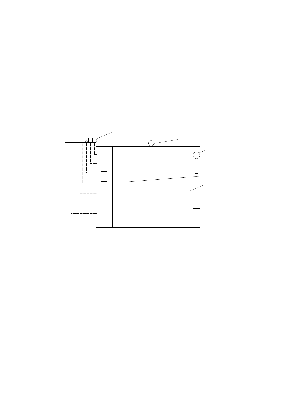
2. Register Diagram
The symbols, and descriptions, used for bit function in each register are shown below.
XXX Register
b7 b6 b5 b4 b3 b2 b1 b0
0
*1
Symbol Address After Reset
XXX XXX 00h
Bit NameBit Symbol
XXX Bit
XXX0
XXX1
Nothing is assigned.
(b2)
When write, should set to “0”. When read, its content is indeterminate.
Reserved Bit
(b3)
XXX Bit
XXX4
XXX5
XXX6
XXX Bit
XXX7
b1 b0
1 0: XXX
0 1: XXX
1 0: Avoid this setting
1 1: XXX
Must set to “0”
Function varies depending on each operation
mode
0: XXX
1: XXX
Function
*5
RW
RW
RW
RW
RW
WO
RW
RO
*1
Blank: Set to “0” or “1” according to the application
0: Set to “0”
1: Set to “1”
X: Nothing is assigned
*2
RW: Read and write
RO: Read only
WO: Write only
−: Nothing is assigned
*3
•Reserved bit
Reserved bit. Set to specified value.
*4
•Nothing is assigned
Nothing is assigned to the bit concerned. As the bit may be use for future functions,
set to “0” when writing to this bit.
•Do not set to this value
The operation is not guaranteed when a value is set.
•Function varies depending on mode of operation
Bit function varies depending on peripheral function mode.
Refer to respective register for each mode.
*2
*3
*4
Page 4

3. M16C Family Documents
The following documents were prepared for the M16C family.
Document Contents
Short Sheet Hardware overview
Data Sheet Hardware overview and electrical characteristics
Hardware Manual Hardware specifications (pin assignments, memory map s, peripheral
specifications, electrical characteristics, timing charts)
Software Manual Detailed description of assembly instructions and microcomputer
performance of each instruction
Application Note • Application examples of peripheral functions
• Sample programs
• Introduction to the basic functions in the M16C family
• Programming method with Assembly and C languages
RENESAS TECHNICAL UPDATE Preliminary report about the specifica tio n of a pr od u ct, a document,
etc.
NOTES:
1. Before using this material, please visit the our website to confirm that this is the most current
document available.
(1)
Page 5

Table of Contents
SFR Page Reference B - 1
1. Overview 1
1.1 Applications.................................................................................................1
1.2 Performance Outline ...................................................................................2
1.3 Block Diagram.............................................................................................5
1.4 Product List .................................................................................................7
1.5 Pin Configuration.......................................................................................14
1.6 Pin Description..........................................................................................25
2. Central Processing Unit (CPU) 30
2.1 Data Registers (R0, R1, R2 and R3).........................................................30
2.2 Address Registers (A0 and A1).................................................................31
2.3 Frame Base Register (FB) ........................................................................31
2.4 Interrupt Table Register (INTB).................................................................31
2.5 Program Counter (PC) ..............................................................................31
2.6 User Stack Pointer (USP) and Interrupt Stack Pointer (ISP).....................31
2.7 Static Base Register (SB)..........................................................................31
2.8 Flag Register (FLG)...................................................................................31
2.8.1 Carry Flag (C Flag).............................................................................31
2.8.2 Debug Flag (D Flag)...........................................................................31
2.8.3 Zero Flag (Z Flag)...............................................................................31
2.8.4 Sign Flag (S Flag)...............................................................................31
2.8.5 Register Bank Select Flag (B Flag)....................................................31
2.8.6 Overflow Flag (O Flag).......................................................................31
2.8.7 Interrupt Enable Flag (I Flag)..............................................................31
2.8.8 Stack Pointer Select Flag (U Flag).....................................................32
2.8.9 Processor Interrupt Priority Level (IPL) ..............................................32
2.8.10 Reserved Area....................................................................................32
3. Memory 33
4. Special Function Register (SFR) 34
5. Reset 40
5.1 Hardware Reset 1 .....................................................................................40
5.1.1 Reset on a Stable Supply Voltage......................................................40
5.1.2 Power-on Reset..................................................................................40
A - 1
Page 6

5.2 Brown-out Detection Reset (Hardware Reset 2).......................................42
5.3 Software Reset..........................................................................................43
5.4 Watchdog Timer Reset.............................................................................43
5.5 Oscillation Stop Detection Reset...............................................................43
5.6 Internal Space. ..........................................................................................44
6. Voltage Detection Circuit 45
6.1 Low Voltage Detection Interrupt................................................................49
6.2 Limitations on Exiting Stop Mode.............................................................51
6.3 Limitations on Exiting Wait Mode..............................................................51
6.4 Cold Start-up / Warm Start-up Determine Function ..................................52
7. Processor Mode 54
7.1 Types of Processor Mode .........................................................................54
7.2 Setting Processor Modes..........................................................................55
8. Bus 59
8.1 Bus Mode..................................................................................................59
8.1.1 Separate Bus......................................................................................59
8.1.2 Multiplexed Bus..................................................................................59
8.2 Bus Control................................................................................................60
8.2.1 Address Bus.......................................................................................60
8.2.2 Data Bus.............................................................................................60
8.2.3 Chip Select Signal..............................................................................60
8.2.4 Read and Write Signals......................................................................63
8.2.5 ALE Signal..........................................................................................63
8.2.6 RDY Signal.........................................................................................64
8.2.7 HOLD Signal.......................................................................................65
8.2.8 8.2.8 BCLK Output .............................................................................65
8.2.9 External Bus Status When Internal Area Accessed ..........................67
8.2.10 Software Wait.....................................................................................68
9. Memory Space Expansion Function 72
9.1 1-Mbyte Mode ...........................................................................................72
9.2 4-Mbyte Mode ...........................................................................................72
9.2.1 9.2.1 Addresses 04000h to 3FFFFh, C0000h to FFFFFh..................72
9.2.2 9.2.2 Addresses 40000h to BFFFFh ..................................................72
A - 2
Page 7

10. Clock Generation Circuit 82
10.1 Types of the Clock Generation Circuit.......................................................82
10.1.1 Main Clock..........................................................................................89
10.1.2 Sub Clock...........................................................................................90
10.1.3 On-chip Oscillator Clock.....................................................................91
10.1.4 PLL Clock...........................................................................................91
10.2 CPU Clock and Peripheral Function Clock................................................93
10.2.1 CPU Clock and BCLK.........................................................................93
10.2.2 Peripheral Function Clock (f1, f2, f8, f32, f1SIO, f2SIO, f8SIO,
f32SIO, fAD, fC32)..............................................................................93
10.3 Clock Output Function............................................................................... 93
10.4 Power Control............................................................................................94
10.4.1 Normal Operating Mode.....................................................................94
10.4.2 Wait Mode ..........................................................................................96
10.4.3 Stop Mode..........................................................................................98
10.5 System Clock Protection Function ..........................................................102
10.6 Oscillation Stop and Re-oscillation Detect Function................................103
10.6.1 Operation When CM27 bit = 0 (Oscillation Stop Detection Reset)...103
10.6.2 Operation When CM27 bit = 0 (Oscillation Stop and Re-oscillation
Detect Interrupt)................................................................................103
10.6.3 How to Use Oscillation Stop and Re-oscillation Detect Function.....104
11. Protection 105
12. Interrupt 106
12.1 Type of Interrupts....................................................................................106
12.2 Software Interrupts..................................................................................107
12.2.1 Undefined Instruction Interrupt.........................................................107
12.2.2 Overflow Interrupt.............................................................................107
12.2.3 BRK Interrupt....................................................................................107
12.2.4 INT Instruction Interrupt....................................................................107
12.3 Hardware Interrupts.................................................................................108
12.3.1 Special Interrupts..............................................................................108
12.3.2 Peripheral Function Interrupts..........................................................108
12.4 Interrupts and Interrupt Vector ................................................................109
12.4.1 Fixed Vector Tables..........................................................................109
12.4.2 Relocatable Vector Tables ...............................................................110
A - 3
Page 8

12.5 Interrupt Control......................................................................................111
12.5.1 I Flag.................................................................................................113
12.5.2 IR Bit.................................................................................................113
12.5.3 ILVL2 to ILVL0 Bits and IPL .............................................................113
12.5.4 Interrupt Sequence...........................................................................114
12.5.5 Interrupt Response Time..................................................................115
12.5.6 Variation of IPL when Interrupt Request is Accepted.......................115
12.5.7 Saving Registers ..............................................................................116
12.5.8 Returning from an Interrupt Routine.................................................118
12.5.9 Interrupt Priority................................................................................118
12.5.10 Interrupt Priority Level Select Circuit................................................119
12.6 INT Interrupt............................................................................................120
12.7 NMI Interrupt ...........................................................................................121
12.8 Key Input Interrupt...................................................................................121
12.9 Address Match Interrupt..........................................................................122
13. Watchdog Timer 124
13.1 Count source protective mode................................................................125
14. DMAC 126
14.1 Transfer Cycles.......................................................................................132
14.1.1 Effect of Source and Destination Addresses....................................132
14.1.2 Effect of BYTE Pin Level..................................................................132
14.1.3 Effect of Software Wait.....................................................................132
14.1.4 Effect of RDY Signal.........................................................................132
14.2 DMA Transfer Cycles..............................................................................134
14.3 DMA Enable............................................................................................135
14.4 DMA Request..........................................................................................135
14.5 Channel Priority and DMA Transfer Timing.............................................136
15. Timers 137
15.1 Timer A....................................................................................................139
15.1.1 Timer Mode ......................................................................................144
15.1.2 Event Counter Mode.........................................................................146
15.1.3 One-shot Timer Mode.......................................................................151
15.1.4 Pulse Width Modulation (PWM) Mode..............................................153
A - 4
Page 9

15.2 Timer B....................................................................................................156
15.2.1 Timer Mode ......................................................................................159
15.2.2 Event Counter Mode.........................................................................160
15.2.3 Pulse Period and Pulse Width Measurement Mode.........................162
16. Three-Phase Motor Control Timer Function 165
17. Serial Interface 176
17.1 UARTi (i=0 to 2) ......................................................................................176
17.1.1 Clock Synchronous Serial I/O Mode.................................................189
17.1.2 Clock Asynchronous Serial I/O (UART) Mode..................................197
17.1.3 Special Mode 1 (I2C mode)..............................................................205
17.1.4 Special Mode 2.................................................................................215
17.1.5 Special Mode 3 (IE mode)................................................................220
17.1.6 Special Mode 4 (SIM Mode) (UART2)..............................................222
17.2 SI/O3 and SI/O4......................................................................................227
17.2.1 SI/Oi Operation Timing.....................................................................231
17.2.2 CLK Polarity Selection......................................................................231
17.2.3 Functions for Setting an SOUTi Initial Value....................................232
18. A/D Converter 233
18.1 Mode Description....................................................................................238
18.1.1 One-Shot Mode................................................................................238
18.1.2 Repeat Mode....................................................................................240
18.1.3 Single Sweep Mode..........................................................................242
18.1.4 Repeat Sweep Mode 0.....................................................................244
18.1.5 Repeat Sweep Mode 1.....................................................................246
18.2 Function...................................................................................................248
18.2.1 Resolution Select Function...............................................................248
18.2.2 Sample and Hold..............................................................................248
18.2.3 Extended Analog Input Pins.............................................................248
18.2.4 18.2.4 External Operation Amplifier (Op-Amp) Connection Mode....248
18.2.5 18.2.5 Current Consumption Reducing Function .............................249
18.2.6 Output Impedance of Sensor under A/D Conversion.......................249
A - 5
Page 10

19. D/A Converter 251
20. CRC Calculation 253
21. Programmable I/O Ports 255
21.1 Port Pi Direction Register (PDi Register, i = 0 to 13) ..............................256
21.2 Port Pi Register (Pi Register, i = 0 to 13)................................................256
21.3 Pull-up Control Register 0 to Pull-up Control Register 3
(PUR0 to PUR3 Registers).....................................................................256
21.4 Port Control Register (PCR Register) .....................................................256
22. Flash Memory Version 270
22.1 Memory Map...........................................................................................272
22.1.1 Boot Mode........................................................................................273
22.2 Functions To Prevent Flash Memory from Rewriting..............................273
22.2.1 ROM Code Protect Function ............................................................273
22.2.2 ID Code Check Function ..................................................................273
22.3 CPU Rewrite Mode..................................................................................275
22.3.1 EW0 Mode........................................................................................276
22.3.2 EW1 Mode........................................................................................276
22.3.3 Flash memory Control Register (FIDR, FMR0 and FMR1 registers)276
22.3.4 Precautions on CPU Rewrite Mode..................................................284
22.3.5 Software Commands.......................................................................286
22.3.6 Data Protect Function.......................................................................291
22.3.7 Status Register.................................................................................291
22.3.8 Full Status Check .............................................................................293
22.4 Standard Serial I/O Mode........................................................................295
22.4.1 ID Code Check Function ..................................................................295
22.4.2 Example of Circuit Application in the Standard Serial I/O Mode ......301
22.5 Parallel I/O Mode.....................................................................................303
22.5.1 User ROM and Boot ROM Areas .....................................................303
22.5.2 ROM Code Protect Function ............................................................303
23. Electrical Characteristics 304
23.1 Electrical Characteristics (M16C/62P).....................................................304
23.2 Electrical Characteristics (M16C/62PT) ..................................................346
A - 6
Page 11

24. Precautions 359
24.1 SFR.........................................................................................................359
24.1.1 Register Settings..............................................................................359
24.2 Reset.......................................................................................................360
24.3 Bus..........................................................................................................361
24.4 PLL Frequency Synthesizer....................................................................362
24.5 Power Control..........................................................................................363
24.6 Protect.....................................................................................................365
24.7 Interrupt...................................................................................................366
24.7.1 Reading address 00000h .................................................................366
24.7.2 Setting the SP...................................................................................366
24.7.3 The NMI Interrupt .............................................................................366
24.7.4 Changing the Interrupt Generate Factor...........................................367
24.7.5 INT Interrupt .....................................................................................367
24.7.6 Rewrite the Interrupt Control Register..............................................368
24.7.7 Watchdog Timer Interrupt.................................................................368
24.8 DMAC......................................................................................................369
24.8.1 Write to DMAE Bit in DMiCON Register...........................................369
24.9 Timers.....................................................................................................370
24.9.1 Timer A.............................................................................................370
24.9.2 Timer B.............................................................................................372
24.10 Serial interface ........................................................................................373
24.10.1 Clock Synchronous Serial I/O...........................................................373
24.10.2 UART................................................................................................374
24.10.3 SI/O3, SI/O4.....................................................................................374
24.11 A/D Converter..........................................................................................375
24.12 Programmable I/O Ports..........................................................................377
24.13 Electric Characteristic Differences Between Mask ROM
and Flash Memory Version Microcomputers...........................................378
24.14 Mask ROM ..............................................................................................378
24.15 Flash Memory Version ............................................................................379
24.15.1 Functions to Inhibit Rewriting Flash Memory Rewrite ......................379
24.15.2 Stop mode........................................................................................379
24.15.3 Wait mode ........................................................................................379
24.15.4
Low power dissipation mode, on-chip oscillator low power dissipation mode
....379
24.15.5 Writing command and data...............................................................379
A - 7
Page 12

24.15.6 Program Command..........................................................................379
24.15.7 Lock Bit Program Command ............................................................379
24.15.8 Operation speed...............................................................................380
24.15.9 Instructions inhibited against use .....................................................380
24.15.10Interrupts ..........................................................................................380
24.15.11How to access..................................................................................380
24.15.12Writing in the user ROM area...........................................................380
24.15.13DMA transfer ....................................................................................381
24.15.14Regarding Programming/Erasing Endurance and Execution Time..381
24.16 Noise.......................................................................................................382
25. Differences Depending on Manufacturing Period 383
Appendix 1. Package Dimensions 385
Appendix 2. Difference between M16C/62P and M16C/30P 387
Register Index 390
A - 8
Page 13
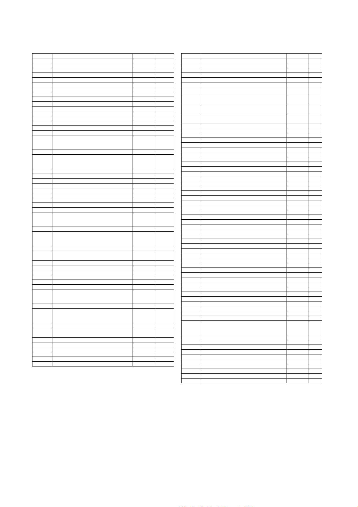
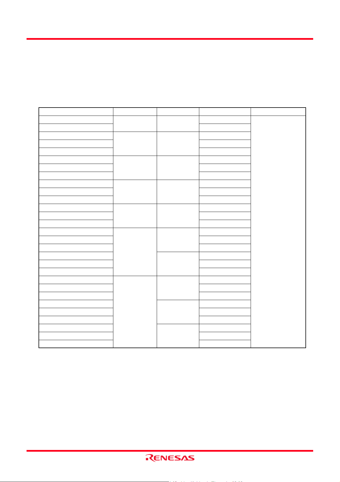
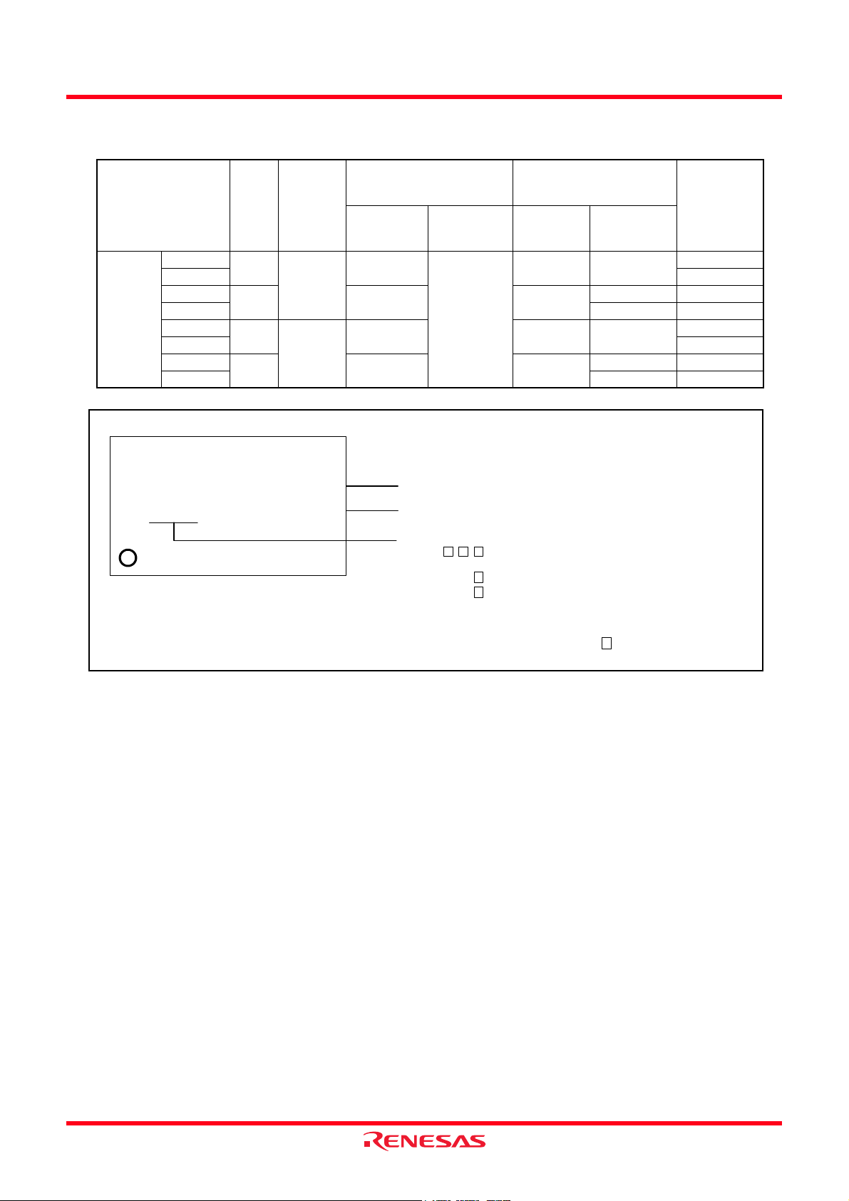
SFR Page Reference
Address Register Symbol Page
0000h
0001h
0002h
0003h
0004h Processor Mode Register 0 PM0 56
0005h Processor Mode Register 1 PM1 57
0006h System Clock Control Register 0 CM0 84
0007h System Clock Control Register 1 CM1 85
0008h Chip Select Control Register CSR 6 1
0009h Address Match Interrupt Enable Register AIER 123
000Ah Protect Register PRCR 105
000Bh Data Bank Register DBR 73
000Ch Oscillation Stop Detection Register CM2 8 6
000Dh
000Eh Watchdog Timer Start Register WDTS 125
000Fh Watchdog Timer Control Register WDC 53, 125
0010h Address Match Interrupt Register 0 RMAD0 123
0011h
0012h
0013h
0014h Address Match Interrupt Register 1 RMAD1 123
0015h
0016h
0017h
0018h
0019h Voltage Detection Register 1 VCR1 46
001Ah Voltage Detection Register 2 VCR2 46
001Bh Chip Select Expansion Control Register CSE 68
001Ch PLL Control Register 0 PLC0 88
001Dh
001Eh Processor Mode Register 2 PM2 87
001Fh Low Voltage Detection In terrupt Register D4INT 47
0020h DMA0 Source Pointer SAR0 131
0021h
0022h
0023h
0024h DMA0 Destination Pointer DAR0 131
0025h
0026h
0027h
0028h DMA0 Transfer Counter TCR0 131
0029h
002Ah
002Bh
002Ch DMA0 Control Register DM0CON 130
002Dh
002Eh
002Fh
0030h DMA1 Source Pointer SAR1 131
0031h
0032h
0033h
0034h DMA1 Destination Pointer DAR1 131
0035h
0036h
0037h
0038h DMA1 Transfer Counter TCR1 131
0039h
003Ah
003Bh
003Ch DMA1 Control Register DM1CON 130
003Dh
003Eh
003Fh
NOTES:
1. Blank columns are all reserved space. No access is allowed.
Address Register Symbol Page
0040h
0041h
0042h
0043h
0044h INT3 Interrupt Control Register INT3IC 112
0045h Timer B5 Interrupt Control Register TB5IC 111
0046h Timer B4 Interrupt Control Registe r , UART1 BUS
0047h Timer B3 Interrupt Control Registe r , UART0 BUS
0048h SI/O4 Interrupt Control Register, INT5 Interrupt
0049h SI/O3 Interrupt Control Register, IINT4 Interrupt
004Ah
004Bh DMA0 Interrupt Control Register DM0IC 111
004Ch DMA1 Interrupt Control Register DM1IC 111
004Dh Key Input Interrupt Control Register KUPIC 111
004Eh A/D Conversion Interrupt Control Register ADIC 11 1
004Fh UART2 Transmit Interrupt Control Register S2TIC 111
0050h UART2 Receive Interrupt Control Register S2RIC 111
0051h UART0 Transmit Interrupt Control Register S0TIC 111
0052h UART0 Receive Interrupt Control Register S0RIC 111
0053h UART1 Transmit Interrupt Control Register S1TIC 111
0054h UART1 Receive Interrupt Control Register S1RIC 111
0055h Timer A0 Interrupt Control Register TA0IC 111
0056h Timer A1 Interrupt Control Register TA1IC 111
0057h Timer A2 Interrupt Control Register TA2IC 111
0058h Timer A3 Interrupt Control Register TA3IC 111
0059h Timer A4 Interrupt Control Register TA4IC 111
005Ah Timer B0 Interrupt Control Register TB0IC 111
005Bh Timer B1 Interrupt Control Register TB1IC 111
005Ch Timer B2 Interrupt Control Register TB2IC 111
005Dh INT0 Interrupt Control Register INT0IC 112
005Eh INT1 Interrupt Control Register INT1IC 112
005Fh INT2 Interrupt Control Register INT2IC 112
0060h
0061h
0062h
0062h
0064h
0065h
0066h
0067h
0068h
0069h
006Ah
006Bh
006Ch
006Dh
006Eh
006Fh
0070h
0071h
0072h
0073h
0074h
0075h
0076h
0077h
0078h
0079h
007Ah
007Bh
007Ch
007Dh
007Eh
007Fh
Collision Detection Interrupt Control Register
Collision Detection Interrupt Control Register
Control Register
Control Register
UART2 Bus Collision Detection Interrupt Control Register
TB4IC,
U1BCNIC
TB3IC,
U0BCNIC
S4IC,
INT5IC
S3IC,
INT4IC
BCNIC 111
111
111
112
112
B - 1
Page 14
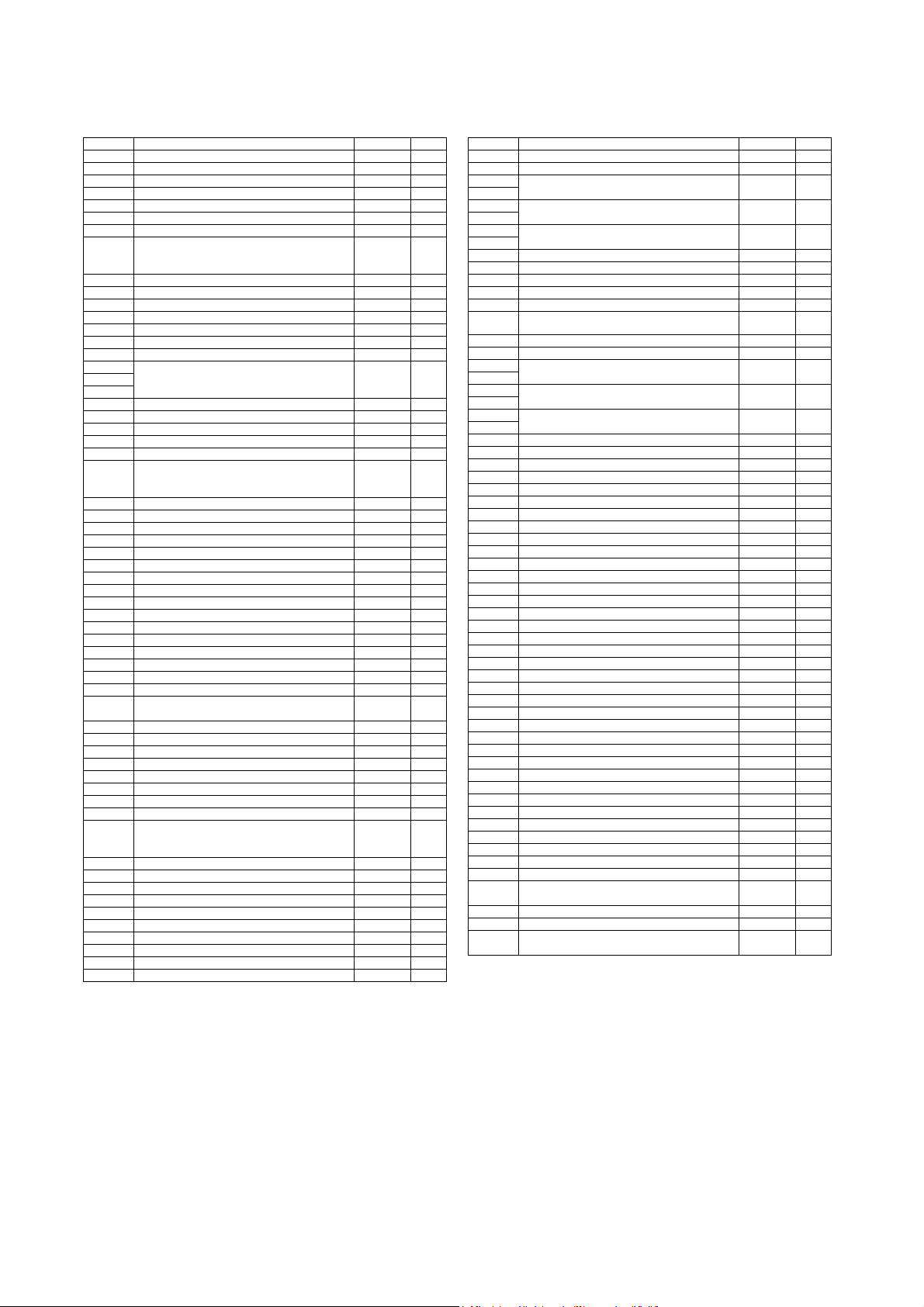
Address Register Symbol Page
0080h
0081h
0082h
0083h
0084h
0085h
0086h
0087h
to
01AFh
01B0h
01B2h
01B3h
01B4h Flash Identification Register FIDR 276
01B5h Flash Memory Control Register 1 FMR1 278
01B6h
01B7h Flash Memory Control Register 0 FMR0 277
01B8h Address Match Interrupt Register 2 RMAD2 123
01B9h
01BAh
01BBh Address Match Interrupt Enable Register 2 AIER2 123
01BCh Address Match Interrupt Register 3 RMAD3 123
01BDh
01BEh
01BFh
01C0h
to
02AFh
0250h
0251h
0252h
0253h
0254h
0255h
0256h
0257h
0258h
0259h
025Ah
025Bh
025Ch
025Dh
025Eh Peripheral Clock Select Register PCLKR 87
025Fh
0260h
0261h
0262h
0263h
0264h
0265h
0266h
0267h
0268h
0269h
026Ah
to
0335h
0336h
0337h
0338h
0339h
033Ah
033Bh
033Ch
033Dh
033Eh
033Fh
Address Register Symbol Page
0340h Timer B3, 4, 5 Count Start Flag TBSR 158
0341h
0342h Timer A1-1 Register TA11 169
0343h
0344h Timer A2-1 Register TA21 169
0345h
0346h Timer A4-1 Register TA41 169
0347h
0348h Three-Phase PWM Control Register 0 INVC0 167
0349h Three-Phase PWM Control Register 1 INVC1 168
034Ah Three-Phase Output Buffer Register 0 IDB0 170
034Bh Three-Phase Output Buffer Register 1 IDB1 170
034Ch Dead Time Timer DTT 171
034Dh Timer B2 Interrupt Occurrence Frequency Se t
034Eh
034Fh
0350h Timer B3 Register TB3 157
0351h
0352h Timer B4 Register TB4 157
0353h
0354h Timer B5 Register TB5 157
0355h
0356h
0357h
0358h
0359h
035Ah
035Bh Timer B3 Mode Register TB3MR 157
035Ch Timer B4 Mode Register TB4MR 157
035Dh Timer B5 Mode Register TB5MR 157
035Eh Interrupt Factor Select Register 2 IFSR2A 120
035Fh Interrupt Factor Select Register IFSR 120
0360h SI/O3 Transmit/Receive Register S3TRR 229
0361h
0362h SI/O3 Control Register S3C 228
0363h SI/O3 Bit Rate Generator S3BRG 229
0364h SI/O4 Transmit/Receive Register S4TRR 229
0365h
0366h SI/O4 Control Register S4C 228
0367h SI/O4 Bit Rate Generator S4BRG 229
0368h
0369h
036Ah
036Bh
036Ch UART0 Special Mode Register 4 U0SMR4 188
036Dh UART0 Special Mode Register 3 U0SMR3 187
036Eh UART0 Special Mode Register 2 U0SMR2 187
036Fh UART0 Special Mode Register U0SMR 186
0370h UART1 Special Mode Register 4 U1SMR4 188
0371h UART1 Special Mode Register 3 U1SMR3 187
0372h UART1 Special Mode Register 2 U1SMR2 187
0373h UART1 Special Mode Register U1SMR 186
0374h UART2 Special Mode Register 4 U2SMR4 188
0375h UART2 Special Mode Register 3 U2SMR3 187
0376h UART2 Special Mode Register 2 U2SMR2 187
0377h UART2 Special Mode Register U2SMR 186
0378h UART2 Transmit/Receive Mode Register U2MR 183
0379h UART2 Bit Rate Generator U2BRG 182
037Ah UART2 Transmit Buffer Register U2TB 181
037Bh
037Ch UART2 Transmit/Receive Control Register 0 U2C0 184
037Dh UART2 Transmit/Receive Control Register 1 U2C1 185
037Eh UART2 Receive Buffer Register U2RB 181
037Fh
Counter
ICTB2 169
NOTES:
1. Blank columns are all reserved space. No access is allowed.
B - 2
Page 15
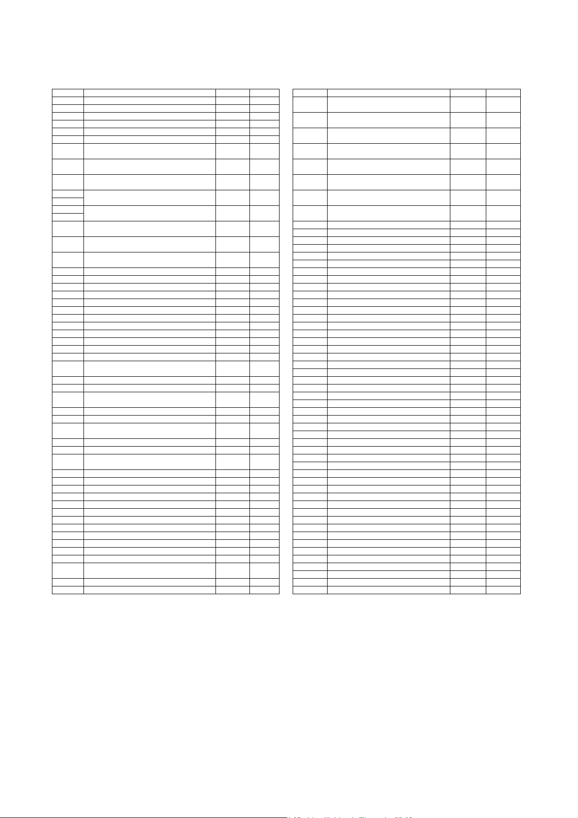
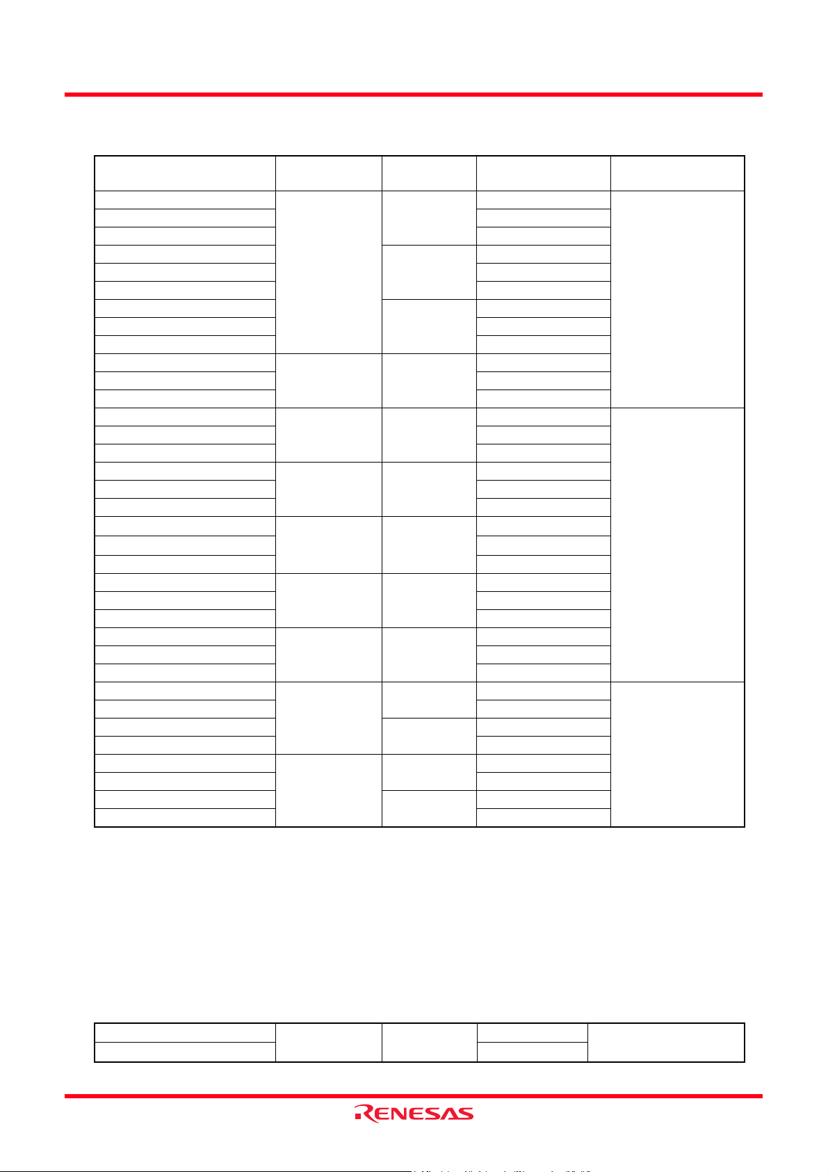
Address Register Symbol Page
0380h Count Start Flag TABSR 141, 158
0381h Clock Prescaler Reset Fag CPSRF 143, 158
0382h One-Shot Start Flag ONSF 14 2
0383h Trigger Select Register TRGSR 142
0384h Up-Down Flag UDF 141
0385h
0386h Timer A0 Register TA0 140
0387h
0388h Timer A1 Register TA1 140
0389h
038Ah Timer A2 Register TA2 140
038Bh
038Ch Timer A3 Register TA3 140
038Dh
038Eh Timer A4 Register TA4 140
038Fh
0390h Timer B0 Register TB0 157
0391h
0392h Timer B1 Register TB1 157
0393h
0394h Timer B2 Register TB2 157
0395h
0396h Timer A0 Mode Register TA0MR 140
0397h Timer A1 Mode Register TA1MR 140
0398h Timer A2 Mode Register TA2MR 140
0399h Timer A3 Mode Register TA3MR 140
039Ah Timer A4 Mode Register TA4MR 140
039Bh Timer B0 Mode Register TB0MR 157
039Ch Timer B1 Mode Register TB1MR 157
039Dh Timer B2 Mode Register TB2MR 157
039Eh Timer B2 Special Mode Register TB2SC 170
039Fh
03A0h UART0 Transmit/Receive Mode Register U0MR 183
03A1h UART0 Bit Rate Generator U0BRG 182
03A2h UART0 Transmit Buffer Register U0TB 181
03A3h
03A4h
03A5h
03A6h UART0 Receive Buffer Register U0RB 181
03A7h
03A8h UART1 Transmit/Receive Mode Register U1MR 183
03A9h UART1 Bit Rate Generator U1BRG 182
03AAh UART1 Transmit Buffer Register U1TB 181
03ABh
03ACh
03ADh
03AEh UART1 Receive Buffer Register U1RB 181
03AFh
03B0h
03B1h
03B2h
03B3h
03B4h
03B5h
03B6h
03B7h
03B8h DMA0 Request Factor Select Register DM0SL 128
03B9h
03BAh DMA1 Request Factor Select Register DM1SL 129
03BBh
03BCh CRC Data Register CRCD 253
03BDh
03BEh CRC Input Register CRCIN 2 53
03BFh
UART0 Transmit/Receive Control Register 0
UART0 Transmit/Receive Control Register 1
UART1 Transmit/Receive Control Register 0
UART1 Transmit/Receive Control Register 1
UART Transmit/Receive Control Register 2
U0C0 184
U0C1 185
U1C0 184
U1C1 185
UCON 186
Address Register Symbol Page
03C0h A/D Register 0 AD0 237
03C1h
03C2h A/D Register 1 AD1 237
03C3h
03C4h A/D Register 2 AD2 237
03C5h
03C6h A/D Register 3 AD3 237
03C7h
03C8h A/D Register 4 AD4 237
03C9h
03CAh A/D Register 5 AD5 237
03CBh
03CCh A/D Register 6 AD6 237
03CDh
03CEh A/D Register 7 AD7 237
03CFh
03D0h
03D1h
03D2h
03D3h
03D4h A/D Control Register 2 ADCON2 236
03D5h
03D6h A/D Control Register 0 ADCON0 235
03D7h A/D Control Register 1 ADCON1 235
03D8h D/A Register 0 DA0 252
03D9h
03DAh D/A Register 1 DA1 252
03DBh
03DCh D/A Control Register DACON 252
03DDh
03DEh Port P14 Control Register PC14 264
03DFh Pull-Up Control Register 3 PUR3 264
03E0h Port P0 Register P0 263
03E1h Port P1 Register P1 263
03E2h Port P0 Direction Register PD0 262
03E3h Port P1 Direction Register PD1 262
03E4h Port P2 Register P2 263
03E5h Port P3 Register P3 263
03E6h Port P2 Direction Register PD2 262
03E7h Port P3 Direction Register PD3 262
03E8h Port P4 Register P4 263
03E9h Port P5 Register P5 263
03EAh Port P4 Direction Register PD4 262
03EBh Port P5 Direction Register PD5 262
03ECh Port P6 Register P6 263
03EDh Port P7 Register P7 263
03EEh Port P6 Direction Register PD6 262
03EFh Port P7 Direction Register PD7 262
03F0h Port P8 Register P8 263
03F1h Port P9 Register P9 263
03F2h Port P8 Direction Register PD8 262
03F3h Port P9 Direction Register PD9 262
03F4h Port P10 Register P10 263
03F5h Port P11 Register P11 263
03F6h Port P10 Direction Register PD10 262
03F7h Port P1 1 D ir ec ti on Register PD11 262
03F8h Port P12 Register P12 263
03F9h Port P13 Register P13 263
03FAh Port P12 Direction Register PD12 262
03FBh Port P13 Direction Register PD13 262
03FCh Pull-Up Control Register 0 PUR0 265
03FDh Pull-Up Control Register 1 PUR1 265
03FEh Pull-Up Control Register 2 PUR2 266
03FFh Port Control Register PCR 266
NOTES:
1. Blank columns are all reserved space. No access is allowed.
B - 3
Page 16
M16C/62P Group (M16C/62P, M16C/62PT)
SINGLE-CHIP 16-BIT CMOS MICROCOMPUTER
1. Overview
The M16C/62P Group (M16C/62P, M16C/62PT) of single-chip microcomputers are built using the high performance
silicon gate CMOS process using a M16C/60 Series CPU core and are packaged in a 80-pin, 100-pin and 128-pin
plastic molded QFP. These single-chip microcom puters operate using soph isticated instructions featuring a high level
of instruction efficiency. With 1M bytes of address space, they are capable of executing instructions at high speed. In
addition, this microcomputer contains a multiplier and DMAC which combined with fast instruction processing
capability, makes it suitable for control of various OA, communication, and industrial equipment which requires highspeed arithmetic/logic operations.
1.1 Applications
Audio, cameras, television, home appliance, office/communications/portable/industrial equipment, automobile,
etc.
Specifications written in this manual are believed to be accurate,
but are not guaranteed to be entirely free of error. Specifications in
this manual may be changed for functional or performance
improvements. Please make sure your manual is the latest edition.
Rev.2.41 Jan 10, 2006 Page 1 of 390
REJ09B0185-0241
Page 17
M16C/62P Group (M16C/62P, M16C/62PT) 1. Overview
1.2 Performance Outline
Table 1.1 to 1.3 list Performance Outline of M16C/62P Group (M16C/62P, M16C/62PT)(128-pin version).
Table 1.1 Performance Outline of M16C/62P Group (M16C/62P, M16C/62PT)(128-pin version)
Item Performance
M16C/62P
CPU Number of Basic Instructions 91 instructions
Minimum Instruction Execution
Time
Operating Mode Single-chip, memory expansion and microprocessor mode
Address Space
Memory Capacity
Peripheral
Function
Port Input/Output : 113 pins, Input : 1 pin
Multifunction Timer Timer A : 16 bits x 5 channels,
Serial Interface 3 channels
A/D Converter 10-bit A/D converter: 1 circuit, 26 channels
D/A Converter 8 bits x 2 channels
DMAC 2 channels
CRC Calculation Circuit CCITT-CRC
Watchdog Timer 15 bits x 1 channel (with prescaler)
Interrupt Internal: 29 sources, External: 8 sources, Software: 4 sources,
Clock Generation Circuit 4 circuits
Oscillation Stop Detection
Function
Voltage Detection Circuit Available (option
Electric
Supply Voltage VCC1=3.0 to 5.5 V, VCC2=2.7V to VCC1 (f(BCLK=24MHz)
Characteristics
Power Consumption 14 mA (VCC1=VCC2=5V, f(BCLK)=24MHz)
Flash memory
version
Program/Erase Supply Voltage 3.3±0.3 V or 5.0±0.5 V
Program and Erase Endurance 100 times (all area)
Operating Ambient Temperature -20 to 85°C,
Package 128-pin plastic mold LQFP
NOTES:
1. I2C bus is a registered trademark of Koninklijke Philips Electronics N. V.
2. IEBus is a registered trademark of NEC Electronics Corporation.
3. See Table 1.8 Product Code for the program and erase endurance, and operating ambient temperature.
In addition 1,000 times/10,000 times are under development as of Jul., 2005. Please inquire about a release
schedule.
4. All options are on request basis.
41.7ns(f(BCLK)=24MHz, VCC1=3.3 to 5.5V)
100ns(f(BCLK)=10MHz, VCC1=2.7 to 5.5V)
1 Mbyte (Available to 4 Mbytes by memory space expansion
function)
See Table 1.4 to 1.5 Product List
Timer B : 16 bits x 6 channels,
Three phase motor control circuit
2
(1)
Clock synchronous, UART, I
C bus
2 channels
Clock synchronous
Priority level: 7 levels
Main clock generation circuit (*),
Subclock generation circuit (*),
On-chip oscillator, PLL synthesizer
(*)Equipped with a built-in feedback resistor.
Stop detection of main clock oscillation, re-oscillation detection
function
(4)
)
VCC1=2.7 to 5.5 V, VCC2=2.7V to VCC1 (f(BCLK=10MHz)
8 mA (VCC1=VCC2=3V, f(BCLK)=10MHz)
1.8µA (VCC1=VCC2=3V, f(XCIN)=32kHz, wait mode)
0.7µA (VCC1=VCC2=3V, stop mode)
or 1,000 times (user ROM area without block A and block 1)
/ 10,000 times (block A, block 1)
-40 to 85°C
(3)
(3)
, IEBus
(2)
Rev.2.41 Jan 10, 2006 Page 2 of 390
REJ09B0185-0241
Page 18
M16C/62P Group (M16C/62P, M16C/62PT) 1. Overview
Table 1.2 Performance Outline of M16C/62P Group (M16C/62P, M16C/62PT)(100-pin version)
Item Performance
M16C/62P M16C/62PT
CPU
Number of Basic Instructions
Minimum Instruction
Execution Time
91 instructions
41.7ns(f(BCLK)=24MHz, VCC1=3.3 to 5.5V)
100ns(f(BCLK)=10MHz, VCC1=2.7 to 5.5V)
Operating Mode Single-chip, memory expansion
41.7ns(f(BCLK)=24MHz, VCC1=4.0 to 5.5V)
Single-chip
and microprocessor mode
Address Space
1 Mbyte (Available to 4 Mbytes by
1 Mbyte
memory space expansion function)
Peripheral
Function
Memory Capacity
Port Input/Output : 87 pins, Input : 1 pin
Multifunction Timer Timer A : 16 bits x 5 channels, Timer B : 16 bits x 6 channels,
See
Table 1.4 to 1.7 Product List
Three phase motor control circuit
Serial Interface 3 channels
Clock synchronous, UART, I
C bus
(1)
, IEBus
(2)
2
2 channels
Clock synchronous
A/D Converter 10-bit A/D converter: 1 circuit, 26 channels
D/A Converter 8 bits x 2 channels
DMAC 2 channels
CRC Calculation Circuit CCITT-CRC
Watchdog Timer 15 bits x 1 channel (with prescaler)
Interrupt
Internal: 29 sources, External: 8 sources, Software: 4 sources, Priority level: 7 levels
Clock Generation Circuit 4 circuits
Main clock generation circuit (*), Subclock generation circuit (*),
On-chip oscillator, PLL synthesizer
(*)Equipped with a built-in feedback resistor.
Oscillation Stop
Stop detection of main clock oscillation, re-oscillation detection function
Detection Function
(5)
)Absent
VCC1=VCC2=4.0 to 5.5V
(f(BCLK=24MHz)
Electric
Characteristics
Voltage Detection Circuit Available (option
Supply Voltage VCC1=3.0 to 5.5 V, VCC2=2.7V to
VCC1 (f(BCLK=24MHz)
VCC1=2.7 to 5.5 V, VCC2=2.7V to
VCC1 (f(BCLK=10MHz)
Power Consumption
14 mA (VCC1=VCC2=5V, f(BCLK)=24MHz)
8 mA (VCC1=VCC2=3V, f(BCLK)=10MHz)
µ
A (VCC1=VCC2=3V, f(XCIN)=32kHz,
1.8
wait mode)
µ
A (VCC1=VCC2=3V, stop mode)
0.7
Flash memory
version
Program/Erase Supply Voltage
Program and Erase
Endurance
3.3±0.3 V or 5.0±0.5 V 5.0±0.5 V
100 times (all area)
or 1,000 times (user ROM area without block A and block 1)
/ 10,000 times (block A, block 1)
Operating Ambient Temperature -20 to 85°C,
-40 to 85°C
(3)
14 mA (VCC1=VCC2=5V, f(BCLK)=24MHz)
2.0
µ
A (VCC1=VCC2=5V, f(XCIN)=32kHz,
wait mode)
µ
A (VCC1=VCC2=5V, stop mode)
0.8
(3)
T version : -40 to 85°C
V version : -40 to 125°C
Package 100-pin plastic mold QFP, LQFP
NOTES:
1. I2C bus is a registered trademark of Koninklijke Philips Electronics N. V.
2. IEBus is a registered trademark of NEC Electronics Corporation.
3. See Table 1.8 and 1.9 Product Code for the program and erase endurance, and operating ambient
temperature.
In addition 1,000 times/10,000 times are under development as of Jul., 2005. Please inquire about a release
schedule.
4. Use the M16C/62PT on VCC1=VCC2
5. All options are on request basis.
(4)
Rev.2.41 Jan 10, 2006 Page 3 of 390
REJ09B0185-0241
Page 19
M16C/62P Group (M16C/62P, M16C/62PT) 1. Overview
Table 1.3 Performance Outline of M16C/62P Group (M16C/62P, M16C/62PT)(80-pin version)
Item Performance
M16C/62P M16C/62PT
CPU
Number of Basic Instructions
Minimum Instruction
Execution Time
91 instructions
41.7ns(f(BCLK)=24MHz, VCC1=3.3 to 5.5V)
100ns(f(BCLK)=10MHz, VCC1=2.7 to 5.5V)
41.7ns(f(BCLK)=24MHz, VCC1=4.0 to 5.5V)
Operating Mode Single-chip mode
Peripheral
Function
Address Space
Memory Capacity
Port Input/Output : 70 pins, Input : 1 pin
Multifunction Timer Timer A : 16 bits x 5 channels (Timer A1 and A2 are internal timer),
1 Mbyte
See Table 1.4 to 1.7 Product List
Timer B : 16 bits x 6 channels (Timer B1 is internal timer)
Serial Interface 2 channels
Clock synchronous, UART, I
C bus
(1)
, IEBus
(2)
2
1 channel
Clock synchronous, I2C bus
(1)
, IEBus
(2)
2 channels
Clock synchronous (1 channel is only transmission)
A/D Converter 10-bit A/D converter: 1 circuit, 26 channels
D/A Converter 8 bits x 2 channels
DMAC 2 channels
CRC Calculation Circuit CCITT-CRC
Watchdog Timer 15 bits x 1 channel (with prescaler)
Interrupt
Internal: 29 sources, External: 5 sources, Software: 4 sources, Priority level: 7 levels
Clock Generation Circuit 4 circuits
Main clock generation circuit (*), Subclock generation circuit (*),
On-chip oscillator, PLL synthesizer
(*)Equipped with a built-in feedback resistor.
Oscillation Stop
Stop detection of main clock oscillation, re-oscillation detection function
Detection Function
(4)
)Absent
VCC1=4.0 to 5.5V, (f(BCLK=24MHz)
14 mA (VCC1=5V, f(BCLK)=24MHz)
2.0µA (VCC1=5V, f(XCIN)=32kHz,
wait mode)
0.8µA (VCC1=5V, stop mode)
Electric
Characteristics
Voltage Detection Circuit Available (option
Supply Voltage
VCC1=3.0 to 5.5 V , (f(BCLK=24MHz)
VCC1=2.7 to 5.5 V , (f(BCLK=10MHz)
Power Consumption
14 mA (VCC1=5V, f(BCLK)=24MHz)
8 mA (VCC1=3V, f(BCLK)=10MHz)
µ
A (VCC1=3V, f(XCIN)=32kHz,
1.8
wait mode)
0.7µA (VCC1=3V, stop mode)
Flash memory
version
Program/Erase Supply Voltage
Program and Erase
Endurance
Operating Ambient Temperature -20 to 85°C,
3.3 ± 0.3V or 5.0 ± 0.5V 5.0 ± 0.5V
100 times (all area)
or 1,000 times (user ROM area without block A and block 1)
/ 10,000 times (block A, block 1)
(3)
T version : -40 to 85°C
-40 to 85°C
(3)
V version : -40 to 125°C
Package 80-pin plastic mold QFP
NOTES:
1. I2C bus is a registered trademark of Koninklijke Philips Electronics N. V.
2. IEBus is a registered trademark of NEC Electronics Corporation.
3. See Table 1.8 and 1.9 Product Code for the program and erase endurance, and operating ambient
temperature.
In addition 1,000 times/10,000 times are under development as of Jul., 2005. Please inquire about a release
schedule.
4. All options are on request basis.
(4)
Rev.2.41 Jan 10, 2006 Page 4 of 390
REJ09B0185-0241
Page 20
M16C/62P Group (M16C/62P, M16C/62PT) 1. Overview
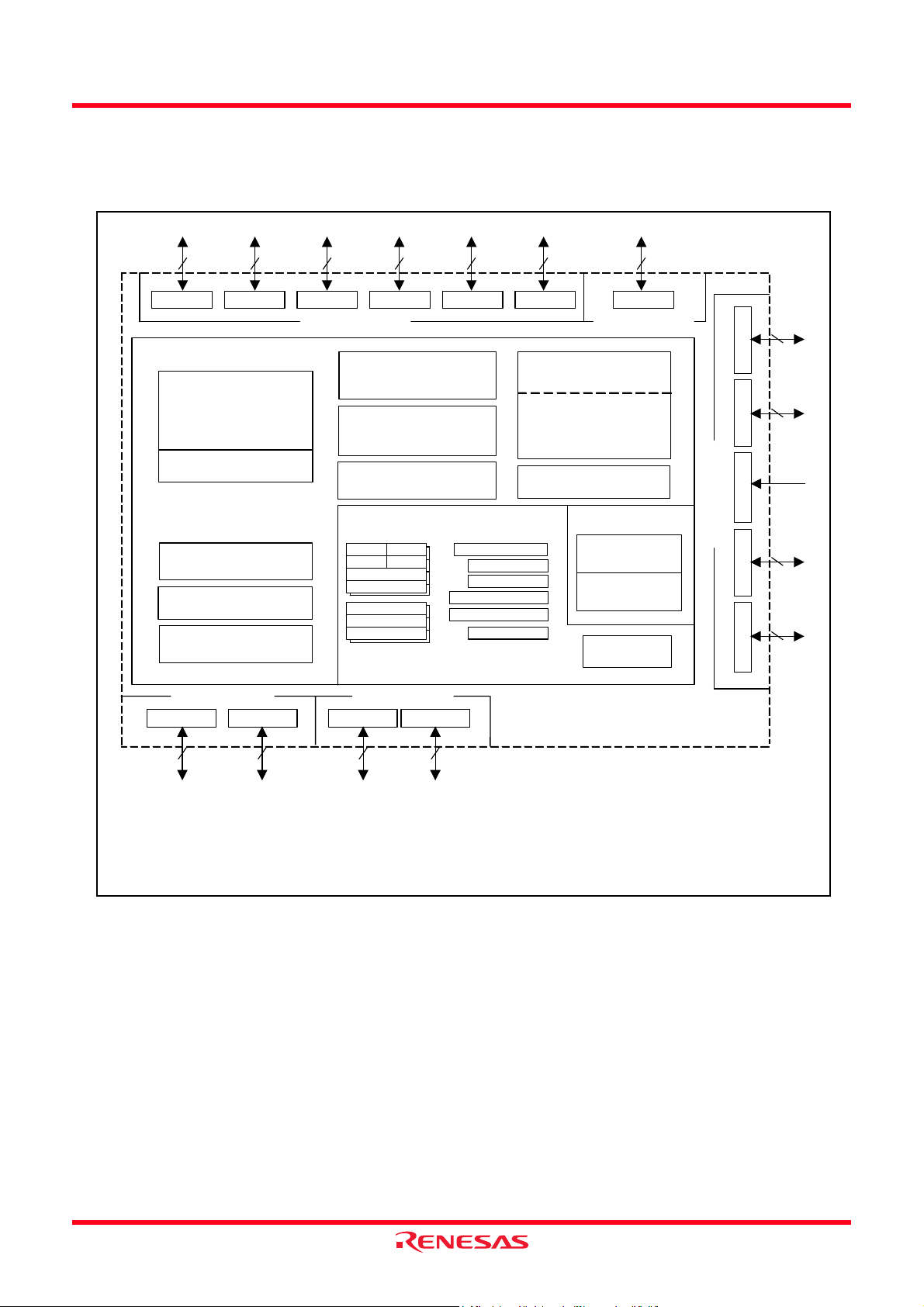
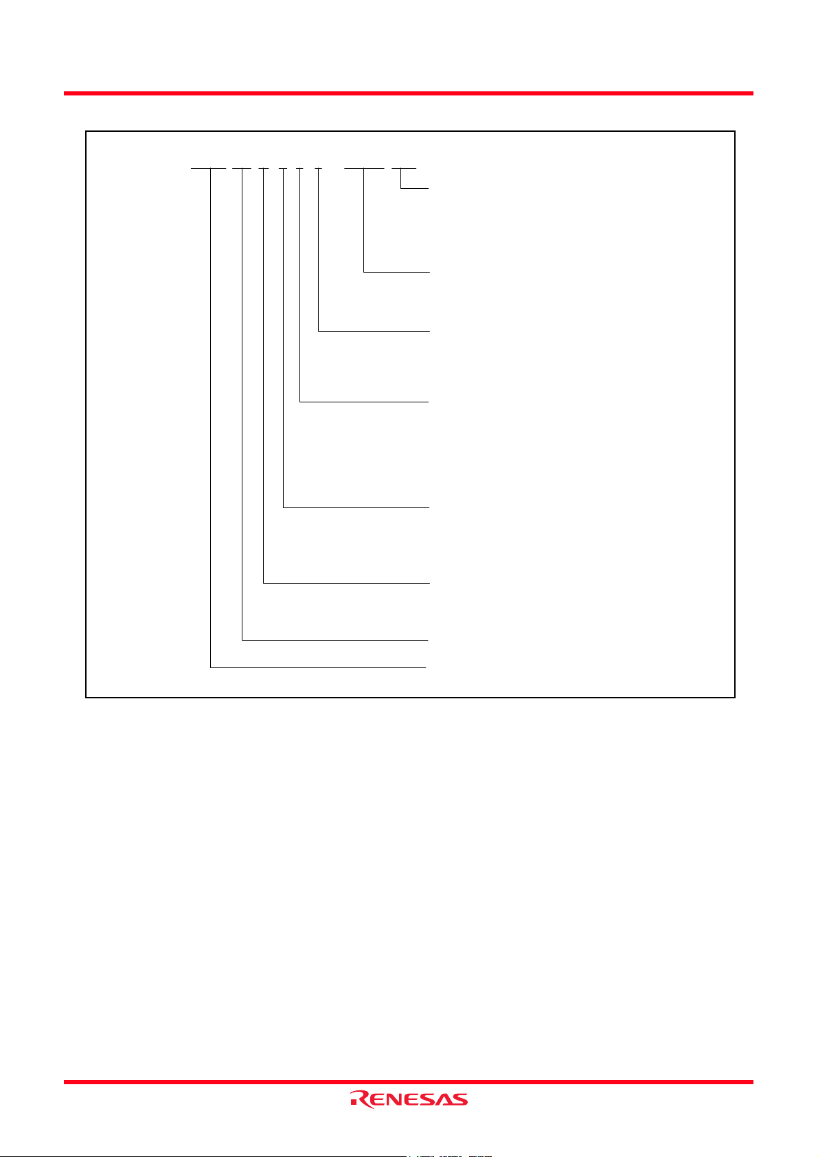
1.3 Block Diagram
Figure 1.1 is a M16C/62P Group (M16C/62P, M16C/62PT) 128-pin and 100-pin version Block Diagram,
Figure 1.2 is a M16C/62P Group (M16C/62P, M16C/62PT) 80-pin version Block Diagram.
8
Port P0
Internal peripheral functions
Port P18Port P2
Timer (16-bit)
Output (timer A): 5
Input (timer B): 6
Three-phase motor
control circuit
Watchdog timer
(15 bits)
DMAC
(2 channels)
D/A converter
(8 bits X 2 channels)
8 8 8 8
Port P4Port P3
Port P5
8
Port P6
<VCC2 ports>(4) <VCC1 ports>(4)
A/D converter
(10 bits X 8 channels
Expandable up to 26 channels)
UART or
clock synchronous serial I/O
(8 bits X 3 channels)
CRC arithmetic circuit (CCITT )
(Polynomial : X
16+X12+X5
+1)
M16C/60 series16-bit CPU core
R0LR0H
R1H R1L
R2
R3
A0
A1
FB
SB
USP
ISP
INTB
PC
FLG
System clock
generation circuit
XIN-XOUT
XCIN-XCOUT
PLL frequency synthesizer
On-chip oscillator
Clock synchronous serial I/O
(8 bits X 2 channels)
Memory
(1)
ROM
(2)
RAM
Multiplier
Port P7
8
7 8 8
<VCC1 ports>(4)
Port P8_5Port P8
Port P9
Port P10
<VCC2 ports>(4)<VCC1 ports>(4)
Port P11 Port P12Port P14
(3)
(3) (3)
Port P13
(3)
8 8 82
NOTES :
1. ROM size depends on microcomputer type.
2. RAM size depends on microcomputer type.
3. Ports P11 to P14 exist only in 128-pin version.
4. Use M16C/62PT on VCC1= VCC2.
Figure 1.1 M16C/62P Group (M16C/62P, M16C/62PT) 128-pin and 100-pin version Block Diagram
Rev.2.41 Jan 10, 2006 Page 5 of 390
REJ09B0185-0241
Page 21
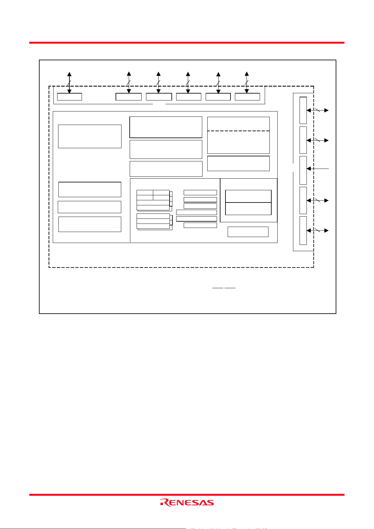
M16C/62P Group (M16C/62P, M16C/62PT) 1. Overview
8
Port P0
Internal peripheral functions
Timer (16-bit)
Output (timer A): 5
Input (timer B): 6
Watchdog timer
(15 bits)
DMAC
(2 channels)
D/A converter
(8 bits X 2 channels)
8
Port P28Port P3
(4)
A/D converter
(10 bits X 8 channels
Expandable up to 26 channels)
UART or
clock synchronous serial I/O (2 channels)
UART (1 channel)
CRC arithmetic circuit (CCITT )
(Polynomial : X
16+X12+X5
M16C/60 series16-bit CPU core
R0LR0H
R1H R1L
R2
R3
A0
A1
FB
4
Port P4
+1)
8
Port P5
System clock
generation circuit
XIN-XOUT
XCIN-XCOUT
PLL frequency synthesizer
(3)
SB
USP
ISP
INTB
PC
FLG
On-chip oscillator
Clock synchronous serial I/O
(8 bits X 2 channels)
8
Port P6
Memory
(1)
ROM
(2)
RAM
Multiplier
Port P7
4 7 7 8
Port P8_5
(4)
Port P9Port P8
Port P10
NOTES :
1. ROM size depends on microcomputer type.
2. RAM size depends on microcomputer type.
3. To use a UART2, set the CRD bit in the U2C0 register to “1” (CTS/RTS function disabled).
4. There is no external connections for port P1, P4_4 to P4_7, P7_2 to P7_5 and P9_1 in 80-pin version.
Set the direction bits in these ports to “1” (output mode), and set the output data to “0” (“L”) using the program.
Figure 1.2 M16C/62P Group (M16C/62P, M16C/62PT) 80-pin version Block Diagram
Rev.2.41 Jan 10, 2006 Page 6 of 390
REJ09B0185-0241
Page 22
M16C/62P Group (M16C/62P, M16C/62PT) 1. Overview
1.4 Product List
Table 1.4 to 1.7 list the product list, Figure 1.3 sho ws the Type No., Memory Size, and Package, Table 1.8 lists the
Product Code of Flash Memory version and ROMless vers ion for M16C/62P, and Table 1.9 lists the Product Code
of Flash Memory version for M16C/62PT. Figure 1.4 shows the Marking Diagram of Flash Memory version and
ROM-less version for M16C/62P (Top View), and Figure 1.5 shows the Marking Diagram of Flash Memory
version for M16C/62PT (Top View) at the time of ROM order.
Table 1.4 Product List (1) (M16C/62P) As of Dec. 2005
Type No. ROM Capacity RAM Capacity Package Type
M30622M6P-XXXFP 48 Kbytes 4 Kbytes PRQP0100JB-A Mask ROM version
M30622M6P-XXXGP PLQP0100KB-A
M30622M8P-XXXFP 64 Kbytes 4 Kbytes PRQP0100JB-A
M30622M8P-XXXGP PLQP0100KB-A
M30623M8P-XXXGP PRQP0080JA-A
M30622MAP-XXXFP 96 Kbytes 5 Kbytes PRQP0100JB-A
M30622MAP-XXXGP PLQP0100KB-A
M30623MAP-XXXGP PRQP0080JA-A
M30620MCP-XXXFP 128 Kbytes 10 Kbytes PRQP0100JB-A
M30620MCP-XXXGP PLQP0100KB-A
M30621MCP-XXXGP PRQP0080JA-A
M30622MEP-XXXFP 192 Kbytes 12 Kbytes PRQP0100JB-A
M30622MEP-XXXGP PLQP0100KB-A
M30623MEP-XXXGP PLQP0128KB-A
M30622MGP-XXXFP 256 Kbytes 12 Kbytes PRQP0100JB-A
M30622MGP-XXXGP PLQP0100KB-A
M30623MGP-XXXGP PLQP0128KB-A
M30624MGP-XXXFP 20 Kbytes PRQP0100JB-A
M30624MGP-XXXGP PLQP0100KB-A
M30625MGP-XXXGP PLQP0128KB-A
M30622MWP-XXXFP 320 Kbytes 16 Kbytes PRQP0100JB-A
M30622MWP-XXXGP PLQP0100KB-A
M30623MWP-XXXGP PLQP0128KB-A
M30624MWP-XXXFP 24 Kbytes PRQP0100JB-A
M30624MWP-XXXGP PLQP0100KB-A
M30625MWP-XXXGP PLQP0128KB-A
M30626MWP-XXXFP 31 Kbytes PRQP0100JB-A
M30626MWP-XXXGP PLQP0100KB-A
M30627MWP-XXXGP PLQP0128KB-A
(D): Under development
NOTES:
1. The old package type numbers of each package type are as follows.
PLQP0128KB-A : 128P6Q-A,
PRQP0100JB-A : 100P6S-A,
PLQP0100KB-A : 100P6Q-A,
PRQP0080JA-A : 80P6S-A
(1)
Remarks
Rev.2.41 Jan 10, 2006 Page 7 of 390
REJ09B0185-0241
Page 23
M16C/62P Group (M16C/62P, M16C/62PT) 1. Overview
Table 1.5 Product List (2) (M16C/62P) As of Dec. 2005
Type No. ROM Capacity
RAM
Capacity
Package Type
(1)
Remarks
M30622MHP-XXXFP 384 Kbytes 16 Kbytes PRQP0100JB-A Mask ROM version
M30622MHP-XXXGP PLQP0100KB-A
M30623MHP-XXXGP PLQP0128KB-A
M30624MHP-XXXFP 24 Kbytes PRQP0100JB-A
M30624MHP-XXXGP PLQP0100KB-A
M30625MHP-XXXGP PLQP0128KB-A
M30626MHP-XXXFP 31 Kbytes PRQP0100JB-A
M30626MHP-XXXGP PLQP0100KB-A
M30627MHP-XXXGP PLQP0128KB-A
M30626MJP-XXXFP (D) 512 Kbytes 31 Kbytes PRQP0100JB-A
M30626MJP-XXXGP (D) PLQP0100KB-A
M30627MJP-XXXGP (D) PLQP0128KB-A
M30622F8PFP 64K+4 Kbytes 4 Kbytes PRQP0100JB-A Flash memory
M30622F8PGP PLQP0100KB-A
version
(2)
M30623F8PGP PRQP0080JA-A
M30620FCPFP 128K+4 Kbytes 10 Kbytes PRQP0100JB-A
M30620FCPGP PLQP0100KB-A
M30621FCPGP PRQP0080JA-A
M3062LFGPFP
M3062LFGPGP
(3)
(3)
(D) 256K+4 Kbytes 20 Kbytes PRQP0100JB-A
(D) PLQP0100KB-A
M30625FGPGP PLQP0128KB-A
M30626FHPFP 384K+4 Kbytes 31 Kbytes PRQP0100JB-A
M30626FHPGP PLQP0100KB-A
M30627FHPGP PLQP0128KB-A
M30626FJPFP 512K+4 Kbytes 31 Kbytes PRQP0100JB-A
M30626FJPGP PLQP0100KB-A
M30627FJPGP PLQP0128KB-A
M30622SPFP − 4 Kbytes PRQP0100JB-A ROM-less version
M30622SPGP PLQP0100KB-A
M30620SPFP 10 Kbytes PRQP0100JB-A
M30620SPGP PLQP0100KB-A
M30624SPFP (D) − 20 Kbytes PRQP0100JB-A
M30624SPGP (D) PLQP0100KB-A
M30626SPFP (D) 31 Kbytes PRQP0100JB-A
M30626SPGP (D) PLQP0100KB-A
(D): Under development
NOTES:
1. The old package type numbers of each package type are as follows.
PLQP0128KB-A : 128P6Q-A,
PRQP0100JB-A : 100P6S-A,
PLQP0100KB-A : 100P6Q-A,
PRQP0080JA-A : 80P6S-A
2. In the flash memory version, there is 4K bytes area (block A).
3. Please use M3062LFGPFP and M3062LFGPGP for your new system instead of M30624FGPFP
and M30624FGPGP. The M16C/62P Group (M16C/62P, M16C/62PT) hardware manual is still good
for M30624FGPFP and M30624FGPGP.
M30624FGPFP 256K+4 Kbytes 20 Kbytes PRQP0100JB-A Fl ash memory version
M30624FGPGP PLQP0100KB-A
Rev.2.41 Jan 10, 2006 Page 8 of 390
REJ09B0185-0241
Page 24
M16C/62P Group (M16C/62P, M16C/62PT) 1. Overview
Table 1.6 Product List (3) (T version (M16C/62PT)) As of Dec. 2005
Type No. ROM Capacity
RAM
Capacity
Package Type
M3062CM6T-XXXFP (D) 48 Kbytes 4 Kbytes PRQP0100JB-A Mask ROM
M3062CM6T-XXXGP (D) PLQP0100KB-A
M3062EM6T-XXXGP (P) PRQP0080JA-A
(1)
version
Remarks
T Version
(High reliability
85°C version)
M3062CM8T-XXXFP (D) 64 Kbytes 4 Kbytes PRQP0100JB-A
M3062CM8T-XXXGP (D) PLQP0100KB-A
M3062EM8T-XXXGP (P) PRQP0080JA-A
M3062CMAT-XXXFP (D) 96 Kbytes 5 Kbytes PRQP0100JB-A
M3062CMAT-XXXGP (D) PLQP0100KB-A
M3062EMAT-XXXGP (P) PRQP0080JA-A
M3062AMCT-XXXFP (D) 128 Kbytes 10 Kbytes PRQP0100JB-A
M3062AMCT-XXXGP (D) PLQP0100KB-A
M3062BMCT-XXXGP (P) PRQP0080JA-A
M3062CF8TFP (D) 64 K+4 Kbytes 4 Kbytes PRQP0100JB-A Flash
M3062CF8TGP PLQP0100KB-A
M3062AFCTFP (D) 128K+4 Kbytes 10 Kbytes PRQP0100JB-A
memory
version
(2)
M3062AFCTGP (D) PLQP0100KB-A
M3062BFCTGP (P) PRQP0080JA-A
M3062JFHTFP (D) 384K+4 Kbytes 31 Kbytes PRQP0100JB-A
M3062JFHTGP (D) PLQP0100KB-A
(D): Under development
(P): Under planning
NOTES:
1. The old package type numbers of each package type are as follows.
PRQP0100JB-A : 100P6S-A,
PLQP0100KB-A : 100P6Q-A,
PRQP0080JA-A : 80P6S-A
2. In the flash memory version, there is 4K bytes area (block A).
Rev.2.41 Jan 10, 2006 Page 9 of 390
REJ09B0185-0241
Page 25
M16C/62P Group (M16C/62P, M16C/62PT) 1. Overview
Table 1.7 Product List (4) (V version (M16C/62PT)) As of Dec. 2005
Type No. ROM Capacity
RAM
Capacity
Package Type
M3062CM6V-XXXFP (P) 48 Kbytes 4 Kbytes PRQP0100JB-A Mask ROM
M3062CM6V-XXXGP (P) PLQP0100KB-A
M3062EM6V-XXXGP (P) PRQP0080JA-A
(1)
version
Remarks
V Version
(High reliability
125°C version)
M3062CM8V-XXXFP (P) 64 Kbytes 4 Kbytes PRQP0100JB-A
M3062CM8V-XXXGP (P) PLQP0100KB-A
M3062EM8V-XXXGP (P) PRQP0080JA-A
M3062CMAV-XXXFP (P) 96 Kbytes 5 Kbytes PRQP0100JB-A
M3062CMAV-XXXGP (P) PLQP0100KB-A
M3062EMAV-XXXGP (P) PRQP0080JA-A
M3062AMCV-XXXFP (D) 128 Kbytes 10 Kbytes PRQP0100JB-A
M3062AMCV-XXXGP (D) PLQP0100KB-A
M3062BMCV-XXXGP (P) PRQP0080JA-A
M3062AFCVFP (D) 128K+4 Kbytes 10 Kbytes PRQP0100JB-A Flash
M3062AFCVGP (D) PLQP0100KB-A
M3062BFCVGP (P) PRQP0080JA-A
memory
version
(2)
M3062JFHVFP (P) 384K+4 Kbytes 31 Kbytes PRQP0100JB-A
M3062JFHVGP (P) PLQP0100KB-A
(D): Under development
(P): Under planning
NOTES:
1. The old package type numbers of each package type are as follows.
PLQP0128KB-A : 128P6Q-A,
PRQP0100JB-A : 100P6S-A,
PLQP0100KB-A : 100P6Q-A,
PRQP0080JA-A : 80P6S-A
2. In the flash memory version, there is 4K bytes area (block A).
Rev.2.41 Jan 10, 2006 Page 10 of 390
REJ09B0185-0241
Page 26
M16C/62P Group (M16C/62P, M16C/62PT) 1. Overview
Type No. M 3 0 6 2 6 M H P - X X X F P
Package type:
FP : Package PRQP0100JB-A (100P6S-A)
GP : Package PRQP0080JA-A (80P6S-A),
PLQP0100KB-A (100P6Q-A),
PLQP0128KB-A (128P6Q-A),
ROM No.
Omitted for flash memory version and
ROMless version
Classification
P : M16C/62P
T : T version (M16C/62PT)
V : V version (M16C/62PT)
Figure 1.3 Type No., Memory Size, and Package
ROM capacity:
6: 48 Kbytes
8: 64 Kbytes
A: 96 Kbytes
C: 128 Kbytes
E: 192 Kbytes
Memory type:
M: Mask ROM version
F: Flash memory version
S: ROM-less version
Shows RAM capacity, pin count, etc
Numeric, Alphabet (L) : M16C/62P
Alphabet (L is excluded.) : M16C/62PT
M16C/62(P) Group
M16C Family
G: 256 Kbytes
W: 320 Kbytes
H: 384 Kbytes
J: 512 Kbytes
Rev.2.41 Jan 10, 2006 Page 11 of 390
REJ09B0185-0241
Page 27
M16C/62P Group (M16C/62P, M16C/62PT) 1. Overview
Table 1.8 Product Code of Flash Memory version and ROMless version for M16C/62P
Flash memory
Version
ROM-less
version
Internal ROM
(User ROM Area Without Block A,
Product
Code
D3 LeadD5 -20°C to 85°C
D7 1,000 10,000 -40°C to 85°C-40°C to 85°C
D9 -20°C to 85°C-20°C to 85°C
U3 Lead-free 100 100 0°C to 60°C-40°C to 85°C
U5 -20°C to 85°C
U7 1,000 10,000 -40°C to 85°C-40°C to 85°C
U9 -20°C to 85°C-20°C to 85°C
D3 LeadD5 -20°C to 85°C
U3 Lead-free −−− −-40°C to 85°C
U5 -20°C to 85°C
Package
included
included
Program
and Erase
Endurance
Block 1)
Temperature
Range
100 0°C to 60°C 100 0°C to 60°C-40°C to 85°C
−− − −-40°C to 85°C
Internal ROM
(Block A, Block 1)
Program
and Erase
Endurance
Temperature
Range
Operating
Ambient
Temperature
M1 6 C
M30626FHPFP
BD5
XXXXXXX
The product without marking of chip version of the flash memory version and the ROMless version
corresponds to the chip version “A”.
Figure 1.4 Marking Diagram of Flash Memory version and ROM-less version for M16C/62P (Top View)
Type No. (See Figure 1.3 Type No., Memory Size, and Package)
Chip version and product code
B : Shows chip version.
Henceforth, whenever it changes a version, it continues with B, C, and D.
D5 : Shows Product code. (See table 1.8 Product Code)
Date code seven digits
Rev.2.41 Jan 10, 2006 Page 12 of 390
REJ09B0185-0241
Page 28
M16C/62P Group (M16C/62P, M16C/62PT) 1. Overview
Table 1.9 Product Code of Flash Memory version for M16C/62PT
Flash
memory
Version
T
Version
Version
V
Version
T
Version
V
Version
T
Version
V
Version
T
Version
V
Internal ROM
(User ROM Area
Product
Code
Package
B Lead-
included
B7 1,000 10,000 -40°C to 85°C-40°C to 85°C
U Lead-free 100 100 0°C to 60°C-40°C to 85°C
U7 1,000 10,000 -40°C to 85°C-40°C to 85°C
Without Block A, Block 1)
Program
and Erase
Endurance
Temperature
Range
100 0°C to 60°C1000°C to 60°C-40°C to 85°C
Internal ROM
(Block A, Block 1)
Program
and Erase
Endurance
Operating
Ambient
Temperature
Range
-40°C to 125°C-40°C to 125°C
-40°C to 125°C-40°C to 125°C
Temperature
-40°C to 125°C
-40°C to 125°C
M1 6 C
M3 0 6 2 J F H TF P
YYY XXXXXXX
Type No. (See Figure 1.3 Type No., Memory Size, and Package)
Date code seven digits
Product code. (See table 1.9 Product Code)
“ ” : Product code “B”
“ P B F ” : Product code “U”
“ B 7 ” : Product code “B”
“ U 7 ” : Product code “U7”
NOTES:
1. : Blank
Figure 1.5 Marking Diagram of Flash Memory version for M16C/62PT (Top View)
Rev.2.41 Jan 10, 2006 Page 13 of 390
REJ09B0185-0241
Page 29
M16C/62P Group (M16C/62P, M16C/62PT) 1. Overview
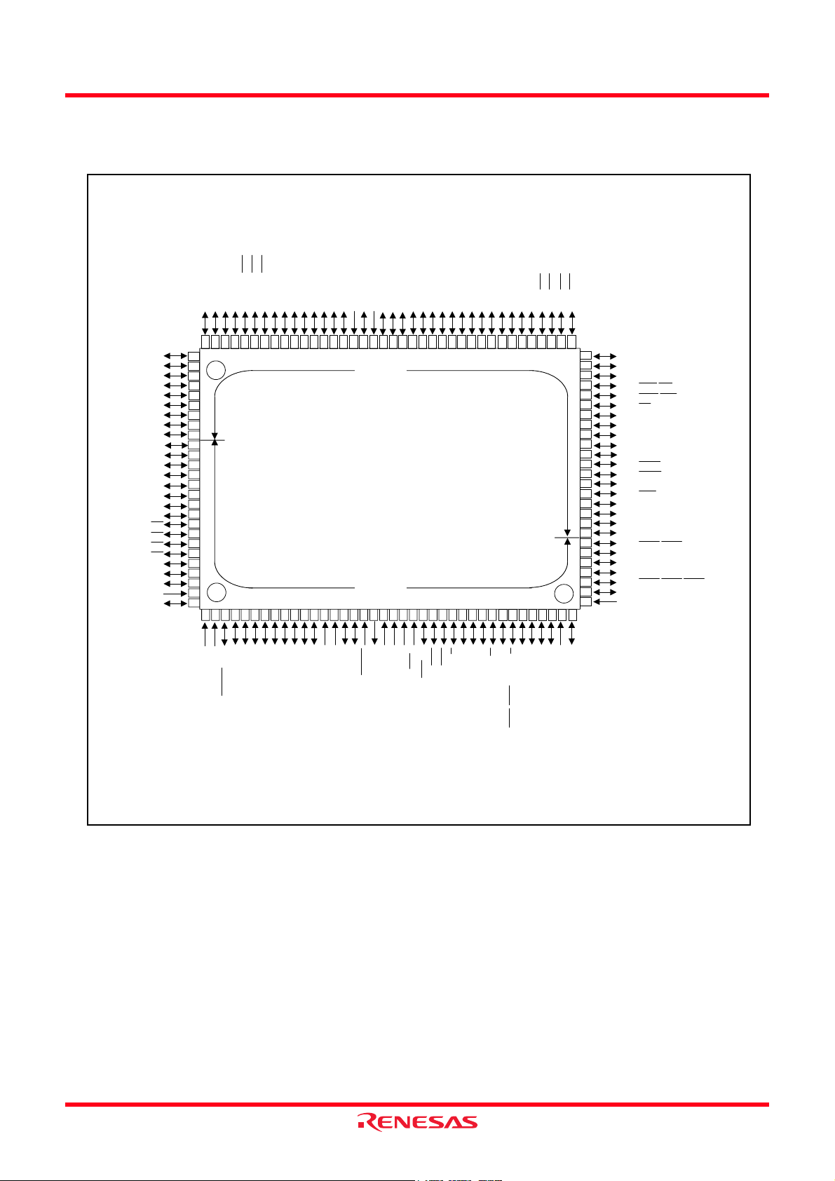
1.5 Pin Configuration
Figures 1.6 to 1.9 show the Pin Configuration (Top View).
PIN CONFIGURATION (top view)
9
D
/
1
_
1
P
P1_0/D8
P0_7/AN0_7/D7
P0_6/AN0_6/D6
P0_5/AN0_5/D5
P0_4/AN0_4/D4
P0_3/AN0_3/D3
P0_2/AN0_2/D2
P0_1/AN0_1/D1
P0_0/AN0_0/D0
P11_7
P11_6
P11_5
P11_4
P11_3
P11_2
P11_1
P11_0
P10_7/AN7/KI3
P10_6/AN6/KI2
P10_5/AN5/KI1
P10_4/AN4/KI0
P10_3/AN3
P10_2/AN2
P10_1/AN1
AVSS
P10_0/AN0
P1_2/D10
P1_3/D11
P1_4/D12
P2_0/AN2_0/A0(/D0/-)
P2_1/AN2_1/A1(/D1/D0)
P2_2/AN2_2/A2(/D2/D1)
P2_3/AN2_3/A3(/D3/D2)
P2_4/AN2_4/A4(/D4/D3)
P2_5/AN2_5/A5(/D5/D4)
P2_6/AN2_6/A6(/D6/D5)
P2_7/AN2_7/A7(/D7/D6)
P3_0/A8(/-/D7)
VCC2
P1_5/D13/INT3
P1_6/D14/INT4
P1_7/D15/INT5
101102
100
103
104
105
106
107
108
109
110
111
112
113
114
115
116
117
118
119
120
121
122
123
124
125
126
127
128
1 2 3 4 5 6 7 8 9101112131415161718192021222324252627282930
M16C/62P Group (M16C/62P)
VSS
<VCC2>
<VCC1>
P12_0
P3_1/A9
P3_2/A10
P3_3/A11
P12_4
P12_3
P12_2
P12_1
(2)
(2)
P3_4/A12
P3_5/A13
P3_6/A14
737475767778798081828384858687888990919293949596979899
P3_7/A15
P4_0/A16
P4_1/A17
P4_2/A18
31 32 33 34 35 36 37
P4_7/CS3
P4_5/CS1
P4_6/CS2
P4_4/CS0
P4_3/A19
66676869707172
65
64
P12_5
63
P12_6
62
P12_7
61
P5_0/WRL/WR
60
P5_1/WRH/BHE
59
P5_2/RD
58
P5_3/BCLK
57
P13_0
56
P13_1
55
P13_2
54
P13_3
53
P5_4/HLDA
52
P5_5/HOLD
51
P5_6/ALE
50
P5_7/RDY/CLKOUT
P13_4
49
48
P13_5
P13_6
47
P13_7
46
45
P6_0/CTS0/RTS0
P6_1/CLK0
44
P6_2/RXD0/SCL0
43
P6_3/TXD0/SDA0
42
P6_4/CTS1/RTS1/CTS0/CLKS1
41
P6_5/CLK1
40
39
38
VSS
VREF
AVCC
P9_3/DA0/TB3IN
P9_4/DA1/TB4IN
P9_7/A D TRG/SIN 4
P9_5/ANEX0/CLK4
P9_2/TB2IN/SOUT3
P9_6/AN EX1/SO UT4
NOTES:
1. P7_0 and P7_1 are N channel open-drain output pins.
2. Use the M16C/62PT on VCC1=VCC2.
BYTE
P14_1
P14_0
CNVSS
P8_7/XCIN
P8_6/XCOUT
P9_1/TB1IN/SIN3
P9_0/TB0IN/CLK3
Figure 1.6 Pin Configuration (Top View)
RESET
(1)
XIN
VSS
VCC1
XOUT
P8_5/NMI
P8_2/INT0
P8_3/INT1
P8_4/IN T 2 /Z P
P7_7/TA3IN
P8_1/TA4IN/U
P7_6/TA3OUT
P7_5/TA2IN/W
P8_0/TA4OUT/U
(1)
VCC1
P7_4/TA2OUT/W
P7_2/CLK2/TA1OUT/V
P7_3/C T S2/RTS2 /T A1IN/V
P6_6/RXD1/SCL1
P6_7/TXD1/SDA1
P7_0/TXD2/SDA2/TA0OUT
P7_1/RXD2/SCL2/TA0IN/TB5IN
Package : PLQP0128KB-A (128P6Q-A)
Rev.2.41 Jan 10, 2006 Page 14 of 390
REJ09B0185-0241
Page 30
M16C/62P Group (M16C/62P, M16C/62PT) 1. Overview
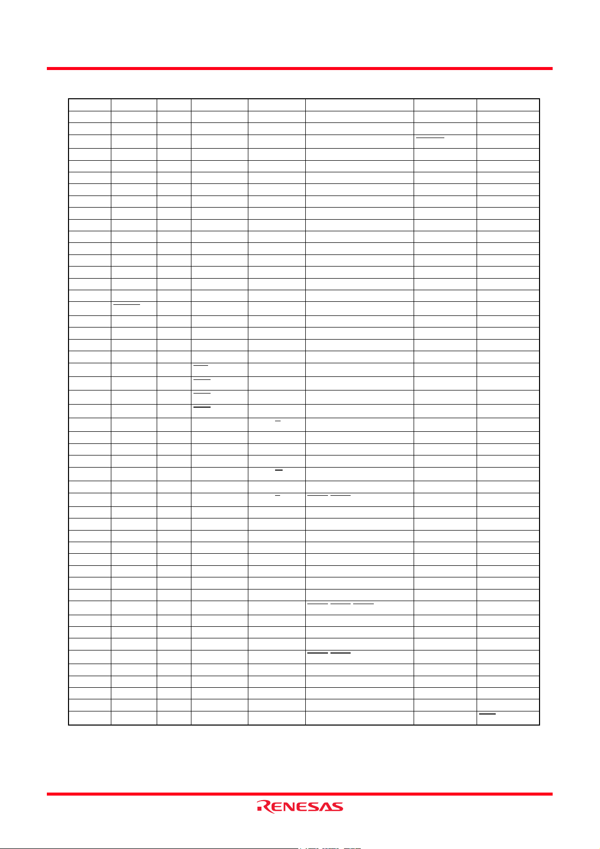
Table 1.10 Pin Characteristics for 128-Pin Package (1)
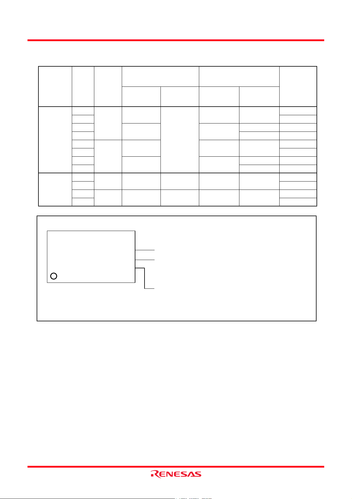
Pin No. Control Pin Port Interrupt Pin Timer Pin UART Pin Analog Pin Bus Control Pin
1VREF
2AVCC
3 P9_7 SIN4 ADTRG
4 P9_6 SOUT4 ANEX1
5 P9_5 CLK4 ANEX0
6P9_4 TB4IN DA1
7P9_3 TB3IN DA0
8 P9_2 TB2IN SOUT3
9 P9_1 TB1IN SIN3
10 P9_0 TB0IN CLK3
11 P14_1
12 P14_0
13 BYTE
14 CNVSS
15 XCIN P8_7
16 XCOUT P8_6
17
RESET
18 XOUT
19 VSS
20 XIN
21 VCC1
22
23
24
25
26
27 P8_0 TA4OUT/U
28 P7_7 TA3IN
29 P7_6 TA3OUT
30
31 P7_4 TA2OUT/W
32
33 P7_2 TA1OUT/V CLK2
34 P7_1 TA0IN/TB5IN RXD2/SCL2
35 P7_0 TA0OUT TXD2/SDA2
36 P6_7 TXD1/SDA1
37 VCC1
38 P6_6 RXD1/SCL1
39 VSS
40 P6_5 CLK1
41
42 P6_3 TXD0/SDA0
43 P6_2 RXD0/SCL0
44 P6_1 CLK0
45
46 P13_7
47 P13_6
48 P13_5
49 P13_4
50
P8_5 NMI
P8_4 INT2
P8_3 INT1
P8_2 INT0
P8_1 TA4IN/U
P7_5 TA2IN/W
P7_3 TA1IN/V
P6_4 CTS1
P6_0 CTS0
P5_7 RDY
ZP
CTS2/RTS2
/RTS1/CTS0/CLKS1
/RTS0
/CLKOUT
Rev.2.41 Jan 10, 2006 Page 15 of 390
REJ09B0185-0241
Page 31

M16C/62P Group (M16C/62P, M16C/62PT) 1. Overview
Table 1.11 Pin Characteristics for 128-Pin Package (2)
Pin No. Control Pin Port Interrupt Pin Timer Pin UART Pin Analog Pin Bus Control Pin
51 P5_6 ALE
52
53
54 P13_3
55 P13_2
56 P13_1
57 P13_0
58 P5_3 BCLK
59
60
61
62 P12_7
63 P12_6
64 P12_5
65
66
67
68
69 P4_3 A19
70 P4_2 A18
71 P4_1 A17
72 P4_0 A16
73 P3_7 A15
74 P3_6 A14
75 P3_5 A13
76 P3_4 A12
77 P3_3 A11
78 P3_2 A10
79 P3_1 A9
80 P12_4
81 P12_3
82 P12_2
83 P12_1
84 P12_0
85 VCC2
86 P3_0 A8(/-/D7)
87 VSS
88 P2_7 AN2_7 A7(/D7/D6)
89 P2_6 AN2_6 A6(/D6/D5)
90 P2_5 AN2_5 A5(/D5/D4)
91 P2_4 AN2_4 A4(/D4/D3)
92 P2_3 AN2_3 A3(/D3/D2)
93 P2_2 AN2_2 A2(/D2/D1)
94 P2_1 AN2_1 A1(/D1/D0)
95 P2_0 AN2_0 A0(/D0/-)
96 P1_7 INT5
97 P1_6 INT4
98 P1_5 INT3
99 P1_4 D12
100 P1_3 D11
P5_5 HOLD
P5_4 HLDA
P5_2 RD
P5_1 WRH
P5_0 WRL
P4_7 CS3
P4_6 CS2
P4_5 CS1
P4_4 CS0
D15
D14
D13
/BHE
/WR
Rev.2.41 Jan 10, 2006 Page 16 of 390
REJ09B0185-0241
Page 32

M16C/62P Group (M16C/62P, M16C/62PT) 1. Overview
Table 1.12 Pin Characteristics for 128-Pin Package (3)
Pin No. Control Pin Port Interrupt Pin Timer Pin UART Pin Analog Pin Bus Control Pin
101 P1_2 D10
102 P1_1 D9
103 P1_0 D8
104 P0_7 AN0_7 D7
105 P0_6 AN0_6 D6
106 P0_5 AN0_5 D5
107 P0_4 AN0_4 D4
108 P0_3 AN0_3 D3
109 P0_2 AN0_2 D2
110 P0_1 AN0_1 D1
111 P0_0 AN0_0 D0
112 P11_7
113 P11_6
114 P11_5
115 P11_4
116 P11_3
117 P11_2
118 P11_1
119 P11_0
120 P10_7 KI3
121 P10_6 KI2
122 P10_5 KI1
123 P10_4 KI0
124 P10_3 AN3
125 P10_2 AN2
126 P10_1 AN1
127 AVSS
128 P10_0 AN0
AN7
AN6
AN5
AN4
Rev.2.41 Jan 10, 2006 Page 17 of 390
REJ09B0185-0241
Page 33

M16C/62P Group (M16C/62P, M16C/62PT) 1. Overview
PIN CONFIGURATION (top view)
P1_0/D8
P1_1/D9
P1_2/D10
P1_3/D11
P1_4/D12
P1_5/D13/INT3
P1_6/D14/INT4
P1_7/D15/INT5
P2_0/AN2_0/A0(/D0/-)
P2_1/AN2_1/A1(/D1/D0)
P2_3/AN 2 _ 3 /A 3 (/D3/D2)
P2_4/AN2_4/A4(/D4/D3)
P2_5/AN2_5/A5(/D5/D4)
P2_2/AN 2_2/A2(/D 2 /D 1 )
P2_6/AN2_6/A6(/D6/D5)
VCC2
VSS
P2_7/AN2_7/A7(/D7/D6)
P3_0/A8(/-/D7)
P3_1/A9
P3_2/A10
P3_3/A11
P3_4/A12
P3_5/A13
P3_6/A14
P3_7/A15
P4_0/A16
P4_1/A17
P4_2/A18
P4_3/A19
P0_7/AN0_7/D7
P0_6/AN0_6/D6
P0_5/AN0_5/D5
P0_4/AN0_4/D4
P0_3/AN0_3/D3
P0_2/AN0_2/D2
P0_1/AN0_1/D1
P0_0/AN0_0/D0
P10_7/AN7/KI3
P10_6/AN6/KI2
P10_5/AN5/KI1
P10_4/AN4/KI0
P10_3/AN3
P10_2/AN2
P10_1/AN1
AVSS
P10_0/AN0
VREF
P9_7/ADTRG/SIN4
NOTES:
1. P7_0 and P7_1 are N channel open-drain output pins.
2. Use the M16C/62PT on VCC1=VCC2.
AVCC
81
82
83
84
85
86
87
88
89
90
91
92
93
94
95
96
97
98
99
00
1
1 2 3 4 5 6 7 8 9 101112131415161718192021222324252627282930
P9_5/ANEX0/CLK4
P9_6/AN E X1/SOU T 4
(M16C/62P, M16C/62PT)
P9_3/DA0/TB3IN
P9_4/DA1/TB4IN
P9_1/TB 1 IN /S IN3
P9_2/TB2IN/SOUT3
<VCC2>
M16C/62P Group
<VCC1>
XIN
BYTE
CNVSS
P8_7/XCIN
P9_0/TB 0 IN/CLK3
VSS
VCC1
XOUT
RESET
P8_6/XCOUT
515253545556575859606162636465666768697071727374757677787980
(2)
(2)
(1)
(1)
P8_5/NMI
P8_2/INT0
P8_3/INT1
P8_4/INT 2 /Z P
P7_7/TA3IN
P8_1/TA 4 IN /U
P7_6/TA3OUT
P7_5/TA 2 IN/W
P8_0/TA4OUT/U
P7_4/TA2OUT/W
P7_2/CLK2/TA1O U T/V
P7_3/CTS2/RTS2/TA1IN/V
P7_0/TXD2/SDA2/TA0OUT
P7_1/RXD2/SCL2/TA0IN/TB5IN
P4_4/CS0
50
49
P4_5/CS1
48
P4_6/CS2
47
P4_7/CS3
46
P5_0/WRL/WR
45
P5_1/WRH/BHE
44
P5_2/RD
43
P5_3/BCLK
42
P5_4/HLDA
41
P5_5/HOLD
40
P5_6/ALE
39
P5_7/RDY/CLKOUT
38
P6_0/CTS0/RTS0
37
P6_1/CLK0
36
P6_2/RXD0/SCL0
35
P6_3/TXD0/SDA0
34
P6_4/CTS1/RTS1/CTS0/CLKS1
33
P6_5/CLK1
32
P6_6/RXD1/SCL1
31
P6_7/TXD1/SDA1
Figure 1.7 Pin Configuration (Top View)
Rev.2.41 Jan 10, 2006 Page 18 of 390
REJ09B0185-0241
Package : PRQP0100JB-A (100P6S-A)
Page 34

M16C/62P Group (M16C/62P, M16C/62PT) 1. Overview
PIN CONFIGURATION (top view)
P1_3/D11
P1_4/D12
P1_5/D13/INT3
P1_6/D14/INT4
P1_7/D15/IN T5
P2_1/AN2_1/A1(/D1/D0)
P2_2/AN2_2/A2(/D2/D1)
P2_3/AN2_3/A3(/D3/D2)
P2_4/AN2_4/A4(/D4/D3)
P2_5/AN2_5/A5(/D5/D4)
P2_0/AN2_0/A0(/D0/-)
P2_6/AN2_6/A6(/D6/D5)
VCC2
VSS
P2_7/AN2_7/A7(/D7/D6)
P3_0/A8(/-/D7)
P3_1/A9
P3_2/A10
P3_3/A11
P3_4/A12
P3_5/A13
P3_6/A14
P3_7/A15
P4_0/A16
P4_1/A17
P1_2/D10
P1_1/D9
P1_0/D8
P0_7/AN0_7/D7
P0_6/AN0_6/D6
P0_5/AN0_5/D5
P0_4/AN0_4/D4
P0_3/AN0_3/D3
P0_2/AN0_2/D2
P0_1/AN0_1/D1
P0_0/AN0_0/D0
P10_7/AN7/KI3
P10_6/AN6/KI2
P10_5/AN5/KI1
P10_4/AN4/KI0
P10_3/AN3
P10_2/AN2
P10_1/AN1
AVSS
P10_0/AN0
VREF
AVCC
P9_7/ADTRG/SIN4
P9_6/ANEX1/SOUT4
P9_5/ANEX0/CLK4
NOTES:
1. P7_0 and P7_1 are N channel open-drain output pins.
2. Use the M16C/62PT on VCC1=VCC2.
76
77
78
79
80
81
82
83
84
85
86
87
88
89
90
91
92
93
94
95
96
97
98
99
00
1
(M16C/62P, M16C/62PT)
12345678910111213141516171819202122232425
P9_3/DA0/TB3IN
P9_4/DA1/TB4IN
P9_2/TB2IN/SOUT3
<VCC2>
M16C/62P Group
<VCC1>
XIN
P8_6/XCOUT
XOUT
RESET
VSS
BYTE
CNVSS
P8_7/XCIN
P9_1/TB1IN/SIN3
P9_0/TB0IN/CLK3
VCC1
57585960616263646566676869707172737475
(2)
(2)
P8_5/NMI
P8_2/INT0
P8_3/INT1
P8_4/INT2/ZP
P8_1/TA4IN/U
P8_0/TA4OUT/U
515253545556
50
49
48
47
46
45
44
43
42
41
40
39
38
37
36
35
34
33
32
31
30
29
28
27
26
P7_7/TA3IN
P7_6/TA3OUT
P7_5/TA2IN/W
P7_4/TA2OUT/W
P7_3/CTS2 /RTS2 /TA1IN /V
P4_2/A18
P4_3/A19
P4_4/CS0
P4_5/CS1
P4_6/CS2
P4_7/CS3
P5_0/WRL/WR
P5_1/WRH/BHE
P5_2/RD
P5_3/BCLK
P5_4/HLDA
P5_5/HOLD
P5_6/ALE
P5_7/RDY/CLKOUT
P6_0/CTS0/RTS0
P6_1/CLK0
P6_2/RXD0/SCL0
P6_3/TXD0/SDA0
P6_4/CTS1/RTS1/CTS0/CLKS1
P6_5/CLK1
P6_6/RXD1/SCL1
P6_7/TXD1/SDA1
P7_0/TXD2/SDA2/TA0OUT
(1)
P7_1/RXD2/SCL2/TA0IN/TB5IN
P7_2/CLK2/TA1OUT/V
(1)
Figure 1.8 Pin Configuration (Top View)
Rev.2.41 Jan 10, 2006 Page 19 of 390
REJ09B0185-0241
Package : PLQP0100KB-A (100P6Q-A)
Page 35

M16C/62P Group (M16C/62P, M16C/62PT) 1. Overview
Table 1.13 Pin Characteristics for 100-Pin Package (1)
Pin No.
FP GP
1 99 P9_6 SOUT4 ANEX1
2 100 P9_5 CLK4 ANEX0
31
4 2 P9_3 TB3IN DA0
5 3 P9_2 TB2IN SOUT3
6 4 P9_1 TB1IN SIN3
7 5 P9_0 TB0IN CLK3
86BYTE
9 7 CNVSS
10 8 XCIN P8_7
11 9 XCOUT P8_6
12 10
13 11 XOUT
14 12 VSS
15 13 XIN
16 14 VCC1
17 15
18 16
19 17
20 18
21 19
22 20 P8_0 TA4OUT/U
23 21 P7_7 TA3IN
24 22 P7_6 TA3OUT
25 23
26 24 P7_4 TA2OUT/W
27 25
28 26 P7_2 TA1OUT/V CLK2
29 27 P7_1 TA0IN/TB5IN RXD2/SCL2
30 28 P7_0 TA0OUT TXD2/SDA2
31 29 P6_7 TXD1/SDA1
32 30 P6_6 RXD1/SCL1
33 31 P6_5 CLK1
34 32
35 33 P6_3 TXD0/SDA0
36 34 P6_2 RXD0/SCL0
37 35 P6_1 CLK0
38 36
39 37
40 38 P5_6 ALE
41 39
42 40
43 41 P5_3 BCLK
44 42
45 43
46 44
47 45
48 46
49 47
50 48
Control Pin Port Interrupt Pin Timer Pin UART Pin Analog Pin Bus Control Pin
P9_4 TB4IN DA1
RESET
P8_5 NMI
P8_4 INT2
P8_3 INT1
P8_2 INT0
P8_1 TA4IN/U
P7_5 TA2IN/W
P7_3 TA1IN/V
P6_4 CTS1
P6_0 CTS0
P5_7 RDY
P5_5 HOLD
P5_4 HLAD
P5_2 RD
P5_1 WRH
P5_0 WRL
P4_7 CS3
P4_6 CS2
P4_5 CS1
P4_4 CS0
ZP
CTS2/RTS2
/RTS1/CTS0/CLKS1
/RTS0
/CLKOUT
/BHE
/WR
Rev.2.41 Jan 10, 2006 Page 20 of 390
REJ09B0185-0241
Page 36

M16C/62P Group (M16C/62P, M16C/62PT) 1. Overview
Table 1.14 Pin Characteristics for 100-Pin Package (2)
Pin No.
FP GP
51 49 P4_3 A19
52 50 P4_2 A18
53
54 52 P4_0 A16
55
56 54 P3_6 A14
57 55 P3_5 A13
58 56 P3_4 A12
59 57 P3_3 A11
60 58 P3_2 A10
61 59 P3_1 A9
62 60 VCC2
63 61 P3_0 A8(/-/D7)
64 62 VSS
65 63 P2_7 AN2_7 A7(/D7/D6)
66 64 P2_6 AN2_6 A6(/D6/D5)
67 65 P2_5 AN2_5 A5(/D5/D4)
68 66 P2_4 AN2_4 A4(/D4/D3)
69 67 P2_3 AN2_3 A3(/D3/D2)
70 68 P2_2 AN2_2 A2(/D2/D1)
71 69 P2_1 AN2_1 A1(/D1/D0)
72 70 P2_0 AN2_0 A0(/D0/-)
73 71
74 72
75 73
76 74 P1_4 D12
77 75 P1_3 D11
78 76 P1_2 D10
79 77 P1_1 D9
80 78 P1_0 D8
81 79 P0_7 AN0_7 D7
82 80 P0_6 AN0_6 D6
83 81 P0_5 AN0_5 D5
84 82 P0_4 AN0_4 D4
85 83 P0_3 AN0_3 D3
86 84 P0_2 AN0_2 D2
87 85 P0_1 AN0_1 D1
88 86 P0_0 AN0_0 D0
89 87
90 88
91 89
92 90
93 91 P10_3 AN3
94 92 P10_2 AN2
95 93 P10_1 AN1
96 94 AVSS
97 95 P10_0 AN0
98 96 VREF
99 97 AVCC
100 98
Control Pin Port Interrupt Pin Timer Pin UART Pin Analog Pin Bus Control Pin
51 P4_1 A17
53
P3_7 A15
P1_7 INT5
P1_6 INT4
P1_5 INT3
P10_7 KI3
P10_6 KI2
P10_5 KI1
P10_4 KI0
P9_7 SIN4 ADTRG
AN7
AN6
AN5
AN4
D15
D14
D13
Rev.2.41 Jan 10, 2006 Page 21 of 390
REJ09B0185-0241
Page 37

M16C/62P Group (M16C/62P, M16C/62PT) 1. Overview
PIN CONFIGURATION (top view)
P3_1
P3_2
P3_3
P3_4
P3_5
P3_6
P3_7
P4_0
P4_1
P0_7/AN0_7
P2_0/AN2_0
P2_1/AN2_1
P2_2/AN2_2
P2_4/AN2_4
P2_5/AN2_5
P2_6/AN2_6
P2_3/AN2_3
P2_7/AN2_7
P3_0
P4_2
56
P0_6/AN0_6
P0_5/AN0_5
P0_4/AN0_4
P0_3/AN0_3
P0_2/AN0_2
P0_1/AN0_1
P0_0/AN0_0
P10_7/AN7/KI3
P10_6/AN6/KI2
P10_5/AN5/KI1
P10_4/AN4/KI0
P10_3/AN3
P10_2/AN2
P10_1/AN1
AVSS
P10_0/AN0
VREF
AVCC
P9_7/ADTRG/SIN4
P9_6/ANEX1/SOUT4
NOTES:
1. P7_0 and P7_1 are N channel open-drain output pins.
61
62
63
64
65
66
67
68
69
70
71
72
73
74
75
76
77
78
79
80
(M16C/62P, M16C/62PT)
1 2 3 4 5 6 7 8 9 1011121314151617
P9_3/DA0/TB3IN
P9_4/DA1/TB4IN
P9_5/AN EX0/CLK 4
P9_2/TB2IN/SOUT3
M16C/62P Group
XIN
VSS
VCC1
P8_5/NMI
P9_0/TB 0 IN /C LK 3
P8_7/XCIN
CNVSS(BYTE)
P8_6/XCOUT
RESET
XOUT
P8_4/INT2/ZP
44454647484950515253545557585960
P8_3/INT1
18 19 20
P8_2/INT0
P8_1/TA4IN
414243
40
39
38
37
36
35
34
33
32
31
30
29
28
27
26
25
24
23
22
21
P7_7/TA3IN
P8_0/TA4OUT
P4_3
P5_0
P5_1
P5_2
P5_3
P5_4
P5_5
P5_6
P5_7/CLKOUT
P6_0/CTS0/RTS0
P6_1/CLK0
P6_2/RXD0/SCL0
P6_3/TXD0/SDA0
P6_4/CTS1/RTS1/CTS0/CLKS1
P6_5/CLK1
P6_6/RXD1/SCL1
P6_7/TXD1/SDA1
P7_0/TXD2/SDA2/TA0OUT
(1)
P7_1/RXD2/SCL2/TA0IN/TB5IN
P7_6/TA3OUT
(1)
Figure 1.9 Pin Configuration (Top View)
Rev.2.41 Jan 10, 2006 Page 22 of 390
REJ09B0185-0241
Package : PRQP0080JA-A (80P6S-A)
Page 38

M16C/62P Group (M16C/62P, M16C/62PT) 1. Overview
Table 1.15 Pin Characteristics for 80-Pin Package (1)
Pin No. Control Pin Port Interrupt Pin Timer Pin UART Pin Analog Pin Bus Control Pin
1 P9_5 CLK4 ANEX0
2P9_4 TB4IN DA1
3
4 P9_2 TB2IN SOUT3
5 P9_0 TB0IN CLK3
CNVSS
6
(BYTE)
7XCIN P8_7
8XCOUTP8_6
9
RESET
10 XOUT
11 VSS
12 XIN
13 VCC1
14
15
16
17
18
19 P8_0 TA4OUT
20 P7_7 TA3IN
21 P7_6 TA3OUT
22 P7_1 TA0IN/TB5IN RXD2/SCL2
23 P7_0 TA0OUT TXD2/SDA2
24 P6_7 TXD1/SDA1
25 P6_6 RXD1/SCL1
26 P6_5 CLK1
27
28 P6_3 TXD0/SDA0
29 P6_2 RXD0/SCL0
30 P6_1 CLK0
31
32
33 P5_6
34
35
36 P5_3
37
38
39
40
41
42
43
44 P3_7
45 P3_6
46 P3_5
47 P3_4
48 P3_3
49 P3_2
50 P3_1
P9_3 TB3IN DA0
P8_5 NMI
P8_4 INT2
P8_3 INT1
P8_2 INT0
P8_1 TA4IN
P6_4 CTS1
P6_0 CTS0
P5_7 CLKOUT
P5_5
P5_4
P5_2
P5_1
P5_0
P4_3
P4_2
P4_1
P4_0
ZP
/RTS1/CTS0/CLKS1
/RTS0
Rev.2.41 Jan 10, 2006 Page 23 of 390
REJ09B0185-0241
Page 39

M16C/62P Group (M16C/62P, M16C/62PT) 1. Overview
Table 1.16 Pin Characteristics for 80-Pin Package (2)
Pin No. Control Pin Port Interrupt Pin Timer Pin UART Pin Analog Pin Bus Control Pin
51 P3_0
52 P2_7 AN2_7
53
54 P2_5 AN2_5
55 P2_4 AN2_4
56 P2_3 AN2_3
57 P2_2 AN2_2
58 P2_1 AN2_1
59 P2_0 AN2_0
60 P0_7 AN0_7
61 P0_6 AN0_6
62 P0_5 AN0_5
63 P0_4 AN0_4
64 P0_3 AN0_3
65 P0_2 AN0_2
66 P0_1 AN0_1
67 P0_0 AN0_0
68
69
70
71
72 P10_3 AN3
73 P10_2 AN2
74 P10_1 AN1
75
AVSS
76 P10_0 AN0
77 VREF
78
AVCC
79
80 P9_6 SOUT4 ANEX1
P2_6 AN2_6
P10_7 KI3
P10_6 KI2
P10_5 KI1
P10_4 KI0
P9_7 SIN4 ADTRG
AN7
AN6
AN5
AN4
Rev.2.41 Jan 10, 2006 Page 24 of 390
REJ09B0185-0241
Page 40

M16C/62P Group (M16C/62P, M16C/62PT) 1. Overview
1.6 Pin Description
Table 1.17 Pin Description (100-pin and 128-pin Version) (1)
Signal Name Pin Name I/O
Type
Power supply
input
Analog power
supply input
Reset input
VCC1,VCC2
VSS
AVCC
AVSS
RESET IVCC1
CNVSS CNVSS I VCC1 Switches processor mode. Connect this pin to VSS to when after
External data
BYTE I VCC1 Switches the data bus in external memory space. The data bus is
bus width
select input
Bus control
(4)
pins
D0 to D7 I/O VCC2 Inputs and outputs data (D0 to D7) when these pins are set as the
D8 to D15 I/O VCC2 Inputs and outputs data (D8 to D15) when external 16-bit data bus
A0 to A19 O VCC2 Output address bits (A0 to A19).
A0/D0 to
A7/D7
A1/D0 to
A8/D7
CS0 to CS3 O VCC2 Output CS0 to CS3 signals. CS0 to CS3 are chip-select signals to
WRL/WR
WRH/BHE
RD
ALE O VCC2 ALE is a signal to latch the address.
HOLD I VCC2 While the HOLD pin is held "L", the microcomputer is placed in a
HLDA O VCC2 In a hold state, HLDA outputs a "L" signal.
RDY I VCC2 While applying a "L" signal to the RDY pin, the microcomputer is
I : Input O : Output I/O : Input and output
Power Supply : Power supplies which relate to the external bus pins are separated as VCC2, thus they can be
interfaced using the different voltage as VCC1.
NOTES:
1. In this manual, hereafter, VCC refers to VCC1 unless otherwise noted.
2. In M16C/62PT, apply 4.0 to 5.5 V to the VCC1 and VCC2 pins. Also the apply condition is that VCC1 = VCC2.
3. When use VCC1 > VCC2, contacts due to some points or restrictions to be checked.
4. Bus control pins in M16C/62PT cannot be used.
Power
Supply
(3)
Description
I − Apply 2.7 to 5.5 V to the VCC1 and VCC2 pins and 0 V to the VSS
pin. The VCC apply condition is that VCC1 ≥ VCC2.
(1, 2)
I VCC1 Applies the power supply for the A/D converter. Connect the AVCC
pin to VCC1. Connect the AVSS pin to VSS.
The microcomputer is in a reset state when applying “L” to the this pin.
a reset to start up in single-chip mode. Connect this pin to VCC1 to
start up in microprocessor mode.
16 bits long when the this pin is held "L" and 8 bits long when the
this pin is held "H". Set it to either one. Connect this pin to VSS
when an single-chip mode.
separate bus.
is set as the separate bus.
I/O VCC2
Input and output data (D0 to D7) and output address bits (A0 to A7) by
timesharing when external 8-bit data bus are set as the multiplexed bus.
I/O VCC2 Input and output data (D0 to D7) and output address bits (A1 to A8)
by timesharing when external 16-bit data bus are set as the
multiplexed bus.
specify an external space.
O VCC2 Output WRL, WRH, (WR, BHE), RD signals. WRL and WRH or
BHE and WR can be switched by program.
, WRH and RD are selected
• WRL
The WRL signal becomes "L" by writing data to an even address in
an external memory space.
The WRH
signal becomes "L" by writing data to an odd address in
an external memory space.
The RD
pin signal becomes "L" by reading data in an external
memory space.
, BHE and RD are selected
• WR
The WR signal becomes "L" by writing data in an external memory space.
signal becomes "L" by reading data in an external memory space.
The RD
The BHE signal becomes "L" by accessing an odd address.
Select WR
, BHE and RD for an external 8-bit data bus.
hold state.
placed in a wait state.
Rev.2.41 Jan 10, 2006 Page 25 of 390
REJ09B0185-0241
Page 41

M16C/62P Group (M16C/62P, M16C/62PT) 1. Overview
Table 1.18 Pin Description (100-pin and 128-pin Version) (2)
Signal Name Pin Name I/O
Type
Main clock
XIN I VCC1 I/O pins for the main clock generation circuit. Connect a ceramic
input
Main clock
XOUT O VCC1
output
Sub clock input XCIN I VCC1 I/O pins for a sub clock oscillation circuit. Connect a crystal
Sub clock
XCOUT O VCC1
output
(2)
BCLK output
BCLK O VCC2 Outputs the BCLK signal.
Clock output CLKOUT O VCC2 The clock of the same cycle as fC, f8, or f32 is outputted.
interrupt
INT
input
interrupt
NMI
INT0 to INT2
to INT5
NT3
NMI
input
Key input
KI0
to KI3
interrupt input
Timer A TA0OUT to
TA4OUT
TA0IN to
TA4IN
ZP I VCC1 Input pin for the Z-phase.
Timer B TB0IN to
TB5IN
Three-phase
motor control
U, U
W, W
, V, V,
output
Serial interface
CTS0
to
CTS2
to
RTS0
RTS2
CLK0 to
CLK4
RXD0 to
RXD2
SIN3, SIN4 I VCC1 These are serial data input pins.
TXD0 to
TXD2
SOUT3,
SOUT4
CLKS1 O VCC1 This is output pin for transfer clock output from multiple pins
2
C mode SD A0 to
I
SDA2
SCL0 to
SCL2
I : Input O : Output I/O : Input and output
Power
Supply
(1)
resonator or crystal oscillator between XIN and XOUT
Description
(3)
. To use
the external clock, input the clock from XIN and leave XOUT open.
(3)
oscillator between XCIN and XCOUT
. To use the external clock,
input the clock from XCIN and leave XCOUT open.
I
VCC1 Input pins for the INT
I
VCC2
I
VCC1 Input pin for the NMI interrupt. Pin states can be read by the P8_5
interrupt.
bit in the P8 register.
I VCC1 Input pins for the key input interrupt.
I/O VCC1 These are timer A0 to timer A4 I/O pins. (however, output of
TA0OUT for the N-channel open drain output.)
I VCC1 These are timer A0 to timer A4 input pins.
I VCC1 These are timer B0 to timer B5 input pins.
O VCC1 These are Three-phase motor control output pins.
I VCC1 These are send control input pins.
O VCC1 These are receive control output pins.
I/O VCC1 These are transfer clock I/O pins.
I VCC1 These are serial data input pins.
O VCC1 These are serial data output pins. (however, output of TXD2 for the
N-channel open drain output.)
O VCC1 These are serial data output pins.
function.
I/O VCC1 These are serial data I/O pins. (however, output of SDA2 for the N-
channel open drain output.)
I/O VCC1 These are transfer clock I/O pins. (however, output of SCL2 for the
N-channel open drain output.)
NOTES:
1. When use VCC1 > VCC2, contacts due to some points or restrictions to be checked.
2. This pin function in M16C/62PT cannot be used.
3. Ask the oscillator maker the oscillation characteristic.
Rev.2.41 Jan 10, 2006 Page 26 of 390
REJ09B0185-0241
Page 42

M16C/62P Group (M16C/62P, M16C/62PT) 1. Overview
Table 1.19 Pin Description (100-pin and 128-pin Version) (3)
Signal Name Pin Name I/O
Type
Reference
VREF I VCC1 Applies the reference voltage for the A/D converter and D/A
voltage input
A/D converter AN0 to AN7,
AN0_0 to
AN0_7,
AN2_0 to
AN2_7
ADTRG
ANEX0 I/O VCC1 This is the extended analog input pin for the A/D converter, and is
ANEX1 I VCC1 This is the extended analog input pin for the A/D converter.
D/A converter DA0 , DA1 O VCC1 This is the output pin for the D/A converter.
I/O port P0_0 to P0_7,
P1_0 to P1_7,
P2_0 to P2_7,
P3_0 to P3_7,
P4_0 to P4_7,
P5_0 to P5_7,
P12_0 to
(2)
P12_7
,
P13_0 to
(2)
P13_7
P6_0 to P6_7,
P7_0 to P7_7,
P9_0 to P9_7,
P10_0 to
P10_7,
P11_0 to
(2)
P11_7
P8_0 to P8_4,
P8_6, P8_7,
P14_0,
(2)
P14_1
Input port P8_5 I
I : Input O : Output I/O : Input and output
Power
Supply
(1)
Description
converter.
I VCC1 Analog input pins for the A/D converter.
I VCC1 This is an A/D trigger input pin.
the output in external op-amp connection mode.
I/O VCC2 8-bit I/O ports in CMOS, having a direction register to select an
input or output.
Each pin is set as an input port or output port. An input port can
be set for a pull-up or for no pull-up in 4-bit unit by program.
I/O VCC1
8-bit I/O ports having equivalent functions to P0.
(however, output of P7_0 and P7_1 for the N-channel open drain
output.)
I/O VCC1 I/O ports having equivalent functions to P0.
VCC1 Input pin for the NMI
interrupt.
Pin states can be read by the P8_5 bit in the P8 register.
NOTES:
1. When use VCC1 > VCC2, contacts due to some points or restrictions to be checked.
2. Ports P11 to P14 in M16C/62P (100-pin version) and M16C/62PT (100-pin version) cannot be used.
Rev.2.41 Jan 10, 2006 Page 27 of 390
REJ09B0185-0241
Page 43

M16C/62P Group (M16C/62P, M16C/62PT) 1. Overview
Table 1.20 Pin Description (80-pin Ve rsion) (1)
Signal Name Pin Name I/O
Type
Power supply
VCC1, VSS
Power
Supply
I − Apply 2.7 to 5.5 V to the VCC1 pin and 0 V to the VSS pin.
(1)
Description
input
Analog power
supply input
Reset input
CNVSS CNVSS
AVCC
AVSS
RESET
(BYTE)
I VCC1 Applies the power supply for the A/D converter. Connect th e
AVCC pin to VCC1. Connect the AVSS pin to VSS.
IVCC1
IVCC1
The microcomputer is in a reset state when applying “L” to the this pin.
Switches processor mode. Connect this pin to VSS to when after a
reset to start up in single-chip mode. Connect this pin to VCC1
start up in microprocessor mode. As for the BYTE pin of the 80-pin
versions, pull-up processing is performed within the microcomputer.
Main clock
input
Main clock
output
XIN I VCC1 I/O pins for the main clock generation circuit. Connect a ceramic
(3)
. To use
XOUT O VCC1
resonator or crystal oscillator between XIN and XOUT
the external clock, input the clock from XIN and leave XOUT
open.
Sub clock input XCIN I VCC1 I/O pins for a sub clock oscillation circuit. Connect a crystal
(3)
Sub clock
output
XCOUT O VCC1
oscillator between XCIN and XCOUT
clock, input the clock from XCIN and leave XCOUT open.
. To use the external
Clock output CLKOUT O VCC2 The clock of the same cycle as fC, f8, or f32 is outputted.
interrupt
INT
INT0 to INT2
I
VCC1 Input pins for the INT interrupt.
input
NMI
interrupt
NMI
I
VCC1 Input pin for the NMI interrupt.
input
Key input
KI0 to KI3
I VCC1 Input pins for the key input interrupt.
interrupt input
Timer A TA0OUT,
TA3OUT,
I/O VCC1 These are Timer A0,Timer A3 and Timer A4 I/O pins. (however,
output of TA0OUT for the N-channel open drain output.)
TA4OUT
TA0IN, TA3IN,
I VCC1 These are Timer A0, Timer A3 and Timer A4 input pins.
TA4IN
ZP I VCC1 Input pin for the Z-phase.
Timer B TB0IN, TB2IN
I VCC1 These are Timer B0, Timer B2 to Timer B5 input pins.
to TB5IN
Serial interface
to CTS1
CTS0
to RTS1
RTS0
CLK0, CLK1,
I VCC1 These are send control input pins.
O VCC1 These are receive control output pins.
I/O VCC1 These are transfer clock I/O pins.
CLK3, CLK4
RXD0 to RXD2 I VCC1 These are serial data input pins.
SIN4 I VCC1 This is serial data input pin.
TXD0 to TXD2 O VCC1 These are serial data output pins. (however, output of TXD2 for
the N-channel open drain output.)
SOUT3,
O VCC1 These are serial data output pins.
SOUT4
CLKS1 O VCC1 This is output pin for transfer clock output from multiple pins
function.
2
C mode SDA0 to SDA2 I/O VCC1 These are serial data I/O pins. (however, output of SDA2 for the
I
N-channel open drain output.)
SCL0 to SCL2 I/O VCC1 These are transfer clock I/O pins. (however, output of SCL2 for
the N-channel open drain output.)
I : Input O : Output I/O : Input and output
(1, 2)
to
NOTES:
1. In this manual, hereafter, VCC refers to VCC1 unless otherwise noted.
2. In M16C/62PT, apply 4.0 to 5.5 V to the VCC1 pin.
3. Ask the oscillator maker the oscillation characteristic.
Rev.2.41 Jan 10, 2006 Page 28 of 390
REJ09B0185-0241
Page 44

M16C/62P Group (M16C/62P, M16C/62PT) 1. Overview
Table 1.21 Pin Description (80-pin Ve rsion) (2)
Signal Name Pin Name I/O
Type
Reference
voltage input
A/D converter AN0 to AN7,
D/A converter DA0 , DA1 O VCC1 This is the output pin for the D/A converter.
I/O port
Input port P8_5 I
I : Input O : Output I/O : Input and output
(1)
VREF I VCC1 Applies the reference voltage for the A/D converter and D/A
AN0_0 to
AN0_7,
AN2_0 to
AN2_7
ADTRG
ANEX0 I/O VCC1 This is the extended analog input pin for the A/D converter, and is
ANEX1 I VCC1 This is the extended analog input pin for the A/D converter.
P0_0 to P0_7,
P2_0 to P2_7,
P3_0 to P3_7,
P5_0 to P5_7,
P6_0 to P6_7,
P10_0 to
P10_7
P8_0 to P8_4,
P8_6, P8_7,
P9_0,
P9_2 to P9_7
P4_0 to P4_3,
P7_0, P7_1,
P7_6, P7_7
Power
(1)
Supply
converter.
I VCC1 Analog input pins for the A/D converter.
I VCC1 This is an A/D trigger input pin.
the output in external op-amp connection mode.
I/O VCC1 8-bit I/O ports in CMOS, having a direction register to select an
input or output.
Each pin is set as an input port or output port. An input port can
be set for a pull-up or for no pull-up in 4-bit unit by program.
I/O VCC1 I/O ports having equivalent functions to P0.
I/O VCC1 I/O ports having equivalent functions to P0.
(however, output of P7_0 and P7_1 for the N-channel open drain
output.)
VCC1 Input pin for the NMI
Pin states can be read by the P8_5 bit in the P8 register.
Description
interrupt.
NOTES:
1. There is no external connections for port P1, P4_4 to P4_7, P7_2 to P7_5 and P9_1 in 80-pin version. Set the
direction bits in these ports to “1” (output mode), and set the output data to “0” (“L”) using the program.
Rev.2.41 Jan 10, 2006 Page 29 of 390
REJ09B0185-0241
Page 45

M16C/62P Group (M16C/62P, M16C/62PT) 2. Central Processing Unit (CPU)
2. Central Processing Unit (CPU)
Figure 2.1 shows the CPU registers. The CPU has 13 registers. Of these, R0, R1, R2, R3, A0, A1 and FB comprise a
register bank. There are two register banks.
b31
R2
R3
b15
b19
INTBH
b19
IPL
b15
b15
b15
b15
R0H
R1H
b8b7 b0
R2
R3
A0
A1
FB
INTBL
PC
USP
ISP
SB
FLG
b7b8
R0L
R1L
Data Registers
Address Registers
Frame Base Registers
b0
Interrupt Table Register
b0
Program Counter
b0
User Stack Pointer
Interrupt Stack Pointer
Static Base Register
b0
Flag Register
b0
CDZSBOIU
Carry Flag
Debug Flag
Zero Flag
Sign Flag
Register Bank Select Flag
Overflow Flag
Interrupt Enable Flag
Stack Pointer Select Flag
Reserved Area
Processor Interrupt Priorit y Le vel
Reserved Area
(1)
(1)
(1)
NOTES:
1. These registers comprise a register bank. There are two register banks.
Figure 2.1 Central Processing Unit Register
2.1 Data Registers (R0, R1, R2 and R3)
The R0 register consists of 16 bits, and is used mainly for transfers and arithmetic/logic operations. R1 to R3 are
the same as R0.
The R0 register can be separated between high (R0H) and low (R0L) for use as two 8-bit data registers.
R1H and R1L are the same as R0H and R0L. Conversely, R2 and R0 can be combined for use as a 32-bit data
register (R2R0). R3R1 is the same as R2R0.
Rev.2.41 Jan 10, 2006 Page 30 of 390
REJ09B0185-0241
Page 46

M16C/62P Group (M16C/62P, M16C/62PT) 2. Central Processing Unit (CPU)
2.2 Address Registers (A0 and A1)
The register A0 consists of 16 bits, and is used for address register indirect addressing and address register relative
addressing. They also are used for transfers and logic/logic operations. A1 is the same as A0.
In some instructions, registers A1 and A0 can be combined for use as a 32-bit address register (A1A0).
2.3 Frame Base Register (FB)
FB is configured with 16 bits, and is used for FB relative addressing.
2.4 Interrupt Table Register (INTB)
INTB is configured with 20 bits, indicating the start address of an interrupt vector table.
2.5 Program Counter (PC)
PC is configured with 20 bits, indicating the address of an instruction to be executed.
2.6 User Stack Pointer (USP) and Interrupt Stack Pointer (ISP)
Stack pointer (SP) comes in two types: USP and ISP, each configured with 16 bits.
Your desired type of stack pointer (USP or ISP) can be selected by the U flag of FLG.
2.7 Static Base Register (SB)
SB is configured with 16 bits, and is used for SB relative addressing.
2.8 Flag Register (FLG)
FLG consists of 11 bits, indicating the CPU status.
2.8.1 Carry Flag (C Flag)
This flag retains a carry, borrow, or shift-out bit that has occurred in the arithmetic/logic unit.
2.8.2 Debug Flag (D Flag)
The D flag is used exclusively for debugging purpose. During normal use, it must be set to “0”.
2.8.3 Zero Flag (Z Flag)
This flag is set to “1” when an arithmetic operation resulted in 0; otherwise, it is “0”.
2.8.4 Sign Flag (S Flag)
This flag is set to “1” when an arithmetic operation resulted in a negative value; otherwise, it is “0”.
2.8.5 Register Bank Select Flag (B Flag)
Register bank 0 is selected when this flag is “0” ; register bank 1 is selected when this flag is “1”.
2.8.6 Overflow Flag (O Flag)
This flag is set to “1” when the operation resulted in an overflow; otherwise, it is “0”.
2.8.7 Interrupt Enable Flag (I Flag)
This flag enables a maskable interrupt.
Maskable interrupts are disabled when the I flag is “0”, and are enabled when the I flag is “1”. The I flag
is cleared to “0” when the interrupt request is accepted.
Rev.2.41 Jan 10, 2006 Page 31 of 390
REJ09B0185-0241
Page 47

M16C/62P Group (M16C/62P, M16C/62PT) 2. Central Processing Unit (CPU)
2.8.8 Stack Pointer Select Flag (U Flag)
ISP is selected when the U flag is “0”; USP is selected when the U flag is “1”.
The U flag is cleared to “0” when a hardware interrupt request is accepted or an INT instruction for software
interrupt Nos. 0 to 31 is executed.
2.8.9 Processor Interrupt Priority Level (IPL)
IPL is configured with three bits, for specification of up to eight processor interrupt priority levels from level 0
to level 7.
If a requested interrupt has priority greater than IPL, the interrupt is enabled.
2.8.10 Reserved Area
When write to this bit, write “0”. When read, its content is indeterminate.
Rev.2.41 Jan 10, 2006 Page 32 of 390
REJ09B0185-0241
Page 48

M16C/62P Group (M16C/62P, M16C/62PT) 3. Memory
3. Memory
Figure 3.1 is a Memory Map of the M16C/62P group. The address space extends the 1M bytes from address 00000h to
FFFFFh.
The internal ROM is allocated in a lower address direction beginning with address FFFFFh . For exam ple, a 64-Kbyte
internal ROM is allocated to the addresses from F0000h to FFFFFh.
As for the flash memory version, 4-Kbyte space (block A) exists in 0F000h to 0FFFFh. 4-Kbyte space is mainly for
storing data. In addition to storing data, 4-Kbyte space also can store programs.
The fixed interrupt vector table is allocated to the addresses from FFFDCh to FFFFFh. Therefore, store the start
address of each interrupt routine here.
The internal RAM is allocated in an upper address direction beginning with address 00400h. For example, a 10-Kbyte
internal RAM is allocated to the addresses from 00400h to 02BFFh. In addition to storing data, the internal RAM also
stores the stack used when calling subroutines and when interrupts are generated.
The SRF is allocated to the addresses from 00000h to 003FFh. Peripheral function control registers are located here.
Of the SFR, any area which has no functions allocated is reserved for future use and cannot be used by users.
The special page vector table is allocated to the addresses from FFE00h to FFFDBh. This vector is used by the JMPS
or JSRS instruction. For details, refer to the M16C/60 and M16C/20 Series Software Manual.
In memory expansion and microprocessor modes, some areas are reserved for future use and cannot be used by users.
Use M16C/62P (80-pin version) and M16C/62PT in single-chip mode. The memory expansion and microprocessor
modes cannot be used
.
00000h
SFR
00400h
Internal RAM
Internal RAM Internal ROM
Address XXXXXh
Size
4 Kbytes 013FFh
5 Kbytes
10 Kbytes
12 Kbytes
20 Kbytes
24 Kbytes
31 Kbytes
017FFh
02BFFh
033FFh
043FFh16 Kbytes
053FFh
063FFh
07FFFh
48 Kbytes
64 Kbytes
96 Kbytes
128 Kbytes
192 Kbytes
256 Kbytes
320 Kbytes
384 Kbytes
512 Kbytes
XXXXXh
0F000h
0FFFFh
(3)
Address YYYYYhSize
F4000h
F0000h
E8000h
E0000h
D0000h
C0000h
B0000h
A0000h
80000h
10000h
27000h
28000h
80000h
YYYYYh
FFFFFh
Reserved area
Internal ROM
(data area)
External area
Reserved area
External area
Reserved area
Internal ROM
(program area)
(1)
(3)
(2)
(5)
NOTES:
1. During memory expansion and microprocessor modes, can be used.
2. In memory expansion mode, can be used.
3. As for the flash memory version, 4-Kbyte space (block A) exists.
4. Shown here is a memory map for the case where the PM10 bit in the PM1 register is “1”
and the PM13 bit in the PM1 register is “1”.
5. When using the masked ROM version, write nothing to internal ROM area.
FFE00h
FFFDCh
FFFFFh
Special page
vector table
Undefined instruction
Overflow
BRK instruction
Address match
Single step
Watchdog timer
DBC
NMI
Reset
Figure 3.1 Memory Map
Rev.2.41 Jan 10, 2006 Page 33 of 390
REJ09B0185-0241
Page 49

M16C/62P Group (M16C/62P, M16C/62PT) 4. S pecial Function Register (SFR)
4. Special Function Register (SFR)
SFR(Special Function Register) is the control register of peripheral functions. Tables 4.1 to 4.6 list the SFR
information.
(2)
(6)
(5, 6)
(5, 6)
(1)
PM0
CSR 00000001b
(3)
(6)
(6)
DBR 00h
CM2 0X000000b
VCR1 00001000b
VCR2 00h
CSE 00h
D4INT 00h
00000000b(CNVSS pin is “L”)
00000011b(CNVSS pin is “H”)
(4)
Table 4.1 SFR Information (1)
Address Register Symbol After Reset
0000h
0001h
0002h
0003h
0004h Processor Mode Register 0
0005h Processor Mode Register 1 PM1 00001000b
0006h System Clock Control Register 0 CM0 01001000b
0007h System Clock Control Register 1 CM1 00100000b
0008h Chip Select Control Register
0009h Address Match Interrupt Enable Register AIER XXXXXX00b
000Ah Protect Register PRCR XX000000b
000Bh Data Bank Register
000Ch Oscillation Stop Detection Register
000Dh
000Eh Watchdog Timer Start Register WDTS XXh
000Fh Watchdog Timer Control Register WDC 00XXXXXXb
0010h Address Match Interrupt Register 0 RMAD0 00h
0011h 00h
0012h X0h
0013h
0014h Address Match Interrupt Register 1 RMAD1 00h
0015h 00h
0016h X0h
0017h
0018h
0019h Voltage Detection Register 1
001Ah Voltage Detection Regist er 2
001Bh Chip Select Expansion Control Register
001Ch PLL Control Register 0 PLC0 0001X010b
001Dh
001Eh Processor Mode Register 2 PM2 XXX00000b
001Fh Low Voltage Detection Interrupt Register
0020h DMA0 Source Pointer SAR0 XXh
0021h XXh
0022h XXh
0023h
0024h DMA0 Destination Pointer DAR0 XXh
0025h XXh
0026h XXh
0027h
0028h DMA0 Transfer Counter TCR0 XXh
0029h XXh
002Ah
002Bh
002Ch DMA0 Control Register DM0CON 00000X00b
002Dh
002Eh
002Fh
0030h DMA1 Source Pointer SAR1 XXh
0031h XXh
0032h XXh
0033h
0034h DMA1 Destination Pointer DAR1 XXh
0035h XXh
0036h XXh
0037h
0038h DMA1 Transfer Counter TCR1 XXh
0039h XXh
003Ah
003Bh
003Ch DMA1 Control Register DM1CON 00000X00b
003Dh
003Eh
003Fh
NOTES:
1. The blank areas are reserved and cannot be accessed by users.
2. The PM00 and PM01 bits do not change at software reset, watchdog timer reset and oscillation stop detection reset.
3. The CM20, CM21, and CM27 bits do not change at oscillation stop detection reset.
4. The WDC5 bit is “0” (cold start) immediately after power-on. I t can only be set to “1” in a program.
5. This register does not change at software reset, watchdog timer reset and oscillation stop detection reset.
6. This register in M16C/62PT cannot be used.
X : Nothing is mapped to this bit
(6)
Rev.2.41 Jan 10, 2006 Page 34 of 390
REJ09B0185-0241
Page 50

M16C/62P Group (M16C/62P, M16C/62PT) 4. S pecial Function Register (SFR)
Table 4.2 SFR Information (2)
Address Register Symbol After Reset
0040h
0041h
0042h
0043h
0044h INT3 Interrupt Control Register INT3IC XX00X000b
0045h Timer B5 Interrupt Control Register TB5IC XXXXX000b
0046h
0047h
0048h SI/O4 Interrupt Control Register, INT5 Interrupt Control Register S4IC, INT5IC XX00X000b
0049h SI/O3 Interrupt Control Register, INT4 Interrupt Control Register S3IC, INT4IC XX00X000b
004Ah UART2 Bus Collision Detection Interrupt Control Register BCNIC XXXXX000b
004Bh DMA0 Interrupt Control Register DM0IC XXXXX000b
004Ch DMA1 Interrupt Control Register DM1IC XXXXX000b
004Dh Key Input Interrupt Control Register KUPIC XXXXX000b
004Eh A/D Conversion Interrupt Control Register ADIC XXXXX000b
004Fh UART2 Transmit Interrupt Control Register S2TIC XXXXX000b
0050h UART2 Receive Interrupt Control Register S2RIC XXXXX000b
0051h UART0 Transmit Interrupt Control Register S0TIC XXXXX000b
0052h UART0 Receive Interrupt Control Register S0RIC XXXXX000b
0053h UART1 Transmit Interrupt Control Register S1TIC XXXXX000b
0054h UART1 Receive Interrupt Control Register S1RIC XXXXX000b
0055h Timer A0 Interrupt Control Register TA0IC XXXXX000b
0056h Timer A1 Interrupt Control Register TA1IC XXXXX000b
0057h Timer A2 Interrupt Control Register TA2IC XXXXX000b
0058h Timer A3 Interrupt Control Register TA3IC XXXXX000b
0059h Timer A4 Interrupt Control Register TA4IC XXXXX000b
005Ah Timer B0 Interrupt Control Register TB0IC XXXXX000b
005Bh Timer B1 Interrupt Control Register TB1IC XXXXX000b
005Ch Timer B2 Interrupt Control Register TB2IC XXXXX000b
005Dh INT0 Interrupt Control Register INT0IC XX00X000b
005Eh INT1 Interrupt Control Register INT1IC XX00X000b
005Fh INT2 Interrupt Control Register INT2IC XX00X000b
0060h
0061h
0062h
0063h
0064h
0065h
0066h
0067h
0068h
0069h
006Ah
006Bh
006Ch
006Dh
006Eh
006Fh
0070h
0071h
0072h
0073h
0074h
0075h
0076h
0077h
0078h
0079h
007Ah
007Bh
007Ch
007Dh
007Eh
007Fh
NOTES:
1. The blank areas are reserved and cannot be accessed by users.
Timer B4 Interrupt Control Register, UART1 BUS Collision Detection Interrupt Control Register
Timer B3 Interrupt Control Register, UART0 BUS Collision Detection Interrupt Control Register
(1)
TB4IC, U1BCNIC XXXXX000b
TB3IC, U0BCNIC XXXXX000b
X : Nothing is mapped to this bit
Rev.2.41 Jan 10, 2006 Page 35 of 390
REJ09B0185-0241
Page 51

M16C/62P Group (M16C/62P, M16C/62PT) 4. S pecial Function Register (SFR)
Table 4.3 SFR Information (3)
Address Register Symbol After Reset
0080h
0081h
0082h
0083h
0084h
0085h
0086h
0087h
to
01AFh
01B0h
01B1h
01B2h
01B3h
01B4h Flash Identificati o n R e gi s t e r
01B5h Flash Memory Control Register 1
01B6h
01B7h Flash Memory Control Register 0
01B8h Address Match Interrupt Register 2 RMAD2 00h
01B9h 00h
01BAh XXh
01BBh Address Match Interrupt Enable Register 2 AIER2 XXXXXX00b
01BCh Address Match Interrupt Register 3 RMAD3 00h
01BDh 00h
01BEh XXh
01C0h
to
024Fh
0250h
0251h
0252h
0253h
0254h
0255h
0256h
0257h
0258h
0259h
025Ah
025Bh
025Ch
025Dh
025Eh Peripheral Clock Select Register PCLKR 00000011b
025Fh
0260h
to
032Fh
0330h
0331h
0332h
0333h
0334h
0335h
0336h
0337h
0338h
0339h
033Ah
033Bh
033Ch
033Dh
033Eh
033Fh
NOTES:
1. The blank areas are reserved and cannot be accessed by users.
2. This register is included in the flash memory version.
(1)
(2)
(2)
(2)
FIDR XXXXXX00b
FMR1 0X00XX0Xb
FMR0 00000001b
X : Nothing is mapped to this bit
Rev.2.41 Jan 10, 2006 Page 36 of 390
REJ09B0185-0241
Page 52

M16C/62P Group (M16C/62P, M16C/62PT) 4. S pecial Function Register (SFR)
Table 4.4 SFR Information (4)
Address Register Symbol After Reset
0340h Timer B3, 4, 5 Count Start Flag TBSR 000XXXXXb
0341h
0342h Timer A1-1 Register TA11 XXh
0343h XXh
0344h Timer A2-1 Register TA21 XXh
0345h XXh
0346h Timer A4-1 Register TA41 XXh
0347h XXh
0348h Three-Phase PWM Control Register 0 INVC0 00h
0349h Three-Phase PWM Control Register 1 INVC1 00h
034Ah Three-Phase Output Buffer Register 0 IDB0 00h
034Bh Three-Phase Output Buffer Register 1 IDB1 00h
034Ch Dead Time Timer DTT XXh
034Dh Timer B2 Interrupt Occurrence Frequency Set Counter ICTB2 XXh
034Eh
034Fh
0350h Timer B3 Register TB3 XXh
0351h XXh
0352h Timer B4 Register TB4 XXh
0353h XXh
0354h Timer B5 Register TB5 XXh
0355h XXh
0356h
0357h
0358h
0359h
035Ah
035Bh Timer B3 Mode Register TB3MR 00XX0000b
035Ch Timer B4 Mode Register TB4MR 00XX0000b
035Dh Timer B5 Mode Register TB5MR 00XX0000b
035Eh Interrupt Factor Select Register 2 IFSR2A 00XXXXXXb
035Fh Interrupt Factor Select Register IFSR 00h
0360h SI/O3 Transmit/Receive Register S3TRR XXh
0361h
0362h SI/O3 Control Register S3C 01000000b
0363h SI/O3 Bit Rate Generator S3BRG XXh
0364h SI/O4 Transmit/Receive Register S4TRR XXh
0365h
0366h SI/O4 Control Register S4C 01000000b
0367h SI/O4 Bit Rate Generator S4BRG XXh
0368h
0369h
036Ah
036Bh
036Ch UART0 Special Mode Register 4 U0SMR4 00h
036Dh UART0 Special Mode Register 3 U0SMR3 000X0X0Xb
036Eh UART0 Special Mode Register 2 U0SMR2 X0000000b
036Fh UART0 Special Mode Register U0SMR X0000000b
0370h UART1 Special Mode Register 4 U1SMR4 00h
0371h UART1 Special Mode Register 3 U1SMR3 000X0X0Xb
0372h UART1 Special Mode Register 2 U1SMR2 X0000000b
0373h UART1 Special Mode Register U1SMR X0000000b
0374h UART2 Special Mode Register 4 U2SMR4 00h
0375h UART2 Special Mode Register 3 U2SMR3 000X0X0Xb
0376h UART2 Special Mode Register 2 U2SMR2 X0000000b
0377h UART2 Special Mode Register U2SMR X0000000b
0378h UART2 Transmit/Receive Mode Register U2MR 00h
0379h UART2 Bit Rate Generator U2BRG XXh
037Ah UART2 Transmit Buffer Register U2TB XXh
037Bh XXh
037Ch UART2 Transmit/Receive Control Register 0 U2C0 00001000b
037Dh UART2 Transmit/Receive Control Register 1 U2C1 00000010b
037Eh UART2 Receive Buffer Register U2RB XXh
037Fh XXh
NOTES:
1. The blank areas are reserved and cannot be accessed by users.
(1)
X : Nothing is mapped to this bit
Rev.2.41 Jan 10, 2006 Page 37 of 390
REJ09B0185-0241
Page 53

M16C/62P Group (M16C/62P, M16C/62PT) 4. S pecial Function Register (SFR)
Table 4.5 SFR Information (5)
Address Register Symbol After Reset
0380h Count Start Flag TABSR 00h
0381h Clock Prescaler Reset Fag CPSRF 0XXXXXXXb
0382h One-Shot Start Flag ONSF 00h
0383h Trigger Select Register TRGSR 00h
0384h Up-Down Flag UDF 00h
0385h
0386h Timer A0 Register TA0 XXh
0387h XXh
0388h Timer A1 Register TA1 XXh
0389h XXh
038Ah Timer A2 Register TA2 XXh
038Bh XXh
038Ch Timer A3 Register TA3 XXh
038Dh XXh
038Eh Timer A4 Register TA4 XXh
038Fh XXh
0390h Timer B0 Register TB0 XXh
0391h XXh
0392h Timer B1 Register TB1 XXh
0393h XXh
0394h Timer B2 Register TB2 XXh
0395h XXh
0396h Timer A0 Mode Register TA0MR 00h
0397h Timer A1 Mode Register TA1MR 00h
0398h Timer A2 Mode Register TA2MR 00h
0399h Timer A3 Mode Register TA3MR 00h
039Ah Timer A4 Mode Register TA4MR 00h
039Bh Timer B0 Mode Register TB0MR 00XX0000b
039Ch Timer B1 Mode Register TB1MR 00XX0000b
039Dh Timer B2 Mode Register TB2MR 00XX0000b
039Eh Timer B2 Special Mode Register TB2SC XXXXXX00b
039Fh
03A0h UART0 Transmit/Receive Mode Register U0MR 00h
03A1h UART0 Bit Rate Generator U0 BRG XXh
03A2h UART0 Transmit Buffer Register U0TB XXh
03A3h XXh
03A4h UART0 Transmit/Receive Control Register 0 U0C0 00001000b
03A5h UART0 Transmit/Receive Control Register 1 U0C1 00XX0010b
03A6h UART0 Receive Buffer Register U0RB XXh
03A7h XXh
03A8h UART1 Transmit/Receive Mode Register U1MR 00h
03A9h UART1 Bit Rate Generator U1 BRG XXh
03AAh UART1 Transmit Buffer Register U1TB XXh
03ABh XXh
03ACh UART1 Transmit/Receive Control Register 0 U1C0 00001000b
03ADh UART1 Transmit/Receive Control Register 1 U1C1 00XX0010b
03AEh UART1 Receive Buffer Register U1RB XXh
03AFh XXh
03B0h UART Transmit/Receive Control Register 2 UCON X0000000b
03B1h
03B2h
03B3h
03B4h
03B5h
03B6h
03B7h
03B8h DMA0 Request Factor Select Register DM0SL 00h
03B9h
03BAh DMA1 Request Factor Select Register DM1SL 00h
03BBh
03BCh CRC Data Register CRCD XXh
03BDh XXh
03BEh CRC Input Register CRCIN XXh
03BFh
NOTES:
1. The blank areas are reserved and cannot be accessed by users.
2. Bit 5 in the Up-down flag is “0” by reset. However, The values in these bits when read are indeterminate.
(1)
(2)
X : Nothing is mapped to this bit
Rev.2.41 Jan 10, 2006 Page 38 of 390
REJ09B0185-0241
Page 54

M16C/62P Group (M16C/62P, M16C/62PT) 4. S pecial Function Register (SFR)
Table 4.6 SFR Information (6)
(1)
Address Register Symbol After Reset
03C0h A/D Register 0 AD0 XXh
03C1h XXh
03C2h A/D Register 1 AD1 XXh
03C3h XXh
03C4h A/D Register 2 AD2 XXh
03C5h XXh
03C6h A/D Register 3 AD3 XXh
03C7h XXh
03C8h A/D Register 4 AD4 XXh
03C9h XXh
03CAh A/D Register 5 AD5 XXh
03CBh XXh
03CCh A/D Register 6 AD6 XXh
03CDh XXh
03CEh A/D Register 7 AD7 XXh
03CFh XXh
03D0h
03D1h
03D2h
03D3h
03D4h A/D Control Register 2 ADCON2 00h
03D5h
03D6h A/D Control Register 0 ADCON0 00000XXXb
03D7h A/D Control Register 1 ADCON1 00h
03D8h D/A Register 0 DA0 00h
03D9h
03DAh D/A Register 1 DA1 00h
03DBh
03DCh D/A Control Register DACON 00h
03DDh
03DEh Port P14 Control Register
03DFh Pull-Up Control Register 3
(3)
(3)
PC14 XX00XXXXb
PUR3 00h
03E0h Port P0 Register P0 XXh
03E1h Port P1 Register P1 XXh
03E2h Port P0 Direction Register PD0 00h
03E3h Port P1 Direction Register PD1 00h
03E4h Port P2 Register P2 XXh
03E5h Port P3 Register P3 XXh
03E6h Port P2 Direction Register PD2 00h
03E7h Port P3 Direction Register PD3 00h
03E8h Port P4 Register P4 XXh
03E9h Port P5 Register P5 XXh
03EAh Port P4 Direction Register PD4 00h
03EBh Port P5 Direction Register PD5 00h
03ECh Port P6 Register P6 XXh
03EDh Port P7 Register P7 XXh
03EEh Port P6 Direction Register PD6 00h
03EFh Port P7 Direction Register PD7 00h
03F0h Port P8 Register P8 XXh
03F1h Port P9 Register P9 XXh
03F2h Port P8 Direction Register PD8 00X00000b
03F3h Port P9 Direction Register PD9 00h
03F4h Port P10 Register P10 XXh
03F5h Port P11 Register
03F6h Port P10 Direction Register PD10 00h
03F7h Port P11 Direction Register
03F8h Port P12 Register
03F9h Port P13 Register
03FAh Port P12 Direction Register
03FBh Port P13 Direction Register
(3)
(3)
(3)
(3)
(3)
(3)
P11 XXh
PD11 00h
P12 XXh
P13 XXh
PD12 00h
PD13 00h
03FCh Pull-Up Control Register 0 PUR0 00h
03FDh Pull-Up Control Register 1 PUR1 00000000b
00000010b
03FEh Pull-Up Control Register 2 PUR2 00h
03FFh Port Control Register PCR 00h
NOTES:
1. The blank areas are reserved and cannot be accessed by users.
2. At hardware reset 1 or hardware reset 2, the register is as follows:
• “00000000b” where “L” is inputted to the CNVSS pin
• “00000010b” where “H” is inputted to the CNVSS pin
At software reset, watchdog timer reset and oscillation stop detection reset, the register is as follows:
• “00000000b” where the PM01 to PM00 bits in the PM0 register are “00b” (single-chip mode).
• “00000010b” where the PM01 to PM00 bits in the PM0 register are “01b” (memory expansion mode) or “11b” (microprocessor mode).
3. These registers do not exist in M16C/62P (80-pin version), and M16C /62PT (80-pin version).
X : Nothing is mapped to this bit
(2)
(2)
Rev.2.41 Jan 10, 2006 Page 39 of 390
REJ09B0185-0241
Page 55

M16C/62P Group (M16C/62P, M16C/62PT) 5. Reset
5. Reset
Hardware reset 1, brown-out detectio n reset (hardware re set 2), software reset, watchdog timer reset and oscillation
stop detection reset are available to reset the microcomputer.
5.1 Hardware Reset 1
The microcomputer resets pins, the CPU and SFR by setting the RESET pin. If the supply voltage meets the
recommended operating conditions, the microcomputer resets all pins w hen an “L” si gnal is app lied to the RESET
pin (see Table 5.1 Pin Status When RESET Pin Level is “L”). The oscillation circuit is also reset and the main
clock starts oscillation. The microcomputer resets the CPU and SFR when the signal applied to the RESET
changes low (“L”) to high (“H”). The microcomputer executes the program in an address indicated by the reset
vector. The internal RAM is not reset. When an “L” signal is applied to the RESET
internal RAM, the internal RAM is in an indeterminate state.
Figure 5.1 shows an Example Reset Circuit. Figure 5.2 shows a Reset Sequence. Table 5.1 lists Pin Status When
RESET
Register (SFR) for SFR states after reset.
Pin Level is “L”. Figure 5.3 shows CPU Register Status After Reset. Refer to 4. Special Function
pin while writing data to the
5.1.1 Reset on a Stable Supply Voltage
(1) Apply “L” to the RESET pin
(2) Apply 20 or more clock cycles to the XIN pin
(3) Apply an “H” signal to the RESET
pin
pin
5.1.2 Power-on Reset
(1) Apply “L” to the RESET pin
(2) Raise the supply voltage to the recommended operating level
(3) Insert td(P-R) ms as wait time for the internal voltage to stabilize
(4) Apply 20 or more clock cycles to the XIN pin
(5) Apply “H” to the RESET
RESET
VCC1
pin
Recommended
operation voltage
VCC1
0V
RESET
0V
0.2VCC1
or below
0.2VCC1 or below
Supply a clock with td(P-R) + 20
or more cycles to the XIN pin
NOTES:
1. If VCC1>VCC2, the VCC2 voltage must be lower than that of VCC1 when the power
is being turned on or off.
Figure 5.1 Example Reset Circuit
Rev.2.41 Jan 10, 2006 Page 40 of 390
REJ09B0185-0241
Page 56

M16C/62P Group (M16C/62P, M16C/62PT) 5. Reset
VCC1, VCC2
XIN
Microprocessor
mode BYTE = H
td(P-R) More than
20 cycles
are needed
RESET
BCLK
Address
RD
WR
CS0
Microprocessor
mode BYTE = L
Address
RD
WR
CS0
Single chip
mode
Address
BCLK 28cycles
FFFFCh
FFFFCh FFFFEh
FFFFCh
FFFFDh
Content of reset vector
FFFFEh
Content of reset vector
FFFFEh
Content of reset vector
Figure 5.2 Reset Sequence
Rev.2.41 Jan 10, 2006 Page 41 of 390
REJ09B0185-0241
Page 57

M16C/62P Group (M16C/62P, M16C/62PT) 5. Reset
Table 5.1 Pin Status When RESET
Pin Level is “L”
Pin Name Status
(1)
CNVSS = VSS
CNVSS = VCC1
BYTE = VSS BYTE = VCC1
P0 Input port Data input Data input
P1 Input port Data input Input port
P2, P3, P4_0 to P4_3 Input port Address output (underfined) Address output (underfined)
P4_4 Input port CS0
output (“H” is output) CS0 output (“H” is output)
P4_5 to P4_7 Input port Input port (Pulled high) Input port (Pulled high)
P5_0 Input port WR
P5_1 Input port BHE
P5_2 Input port RD
output (“H” is output) WR output (“H” is output)
output (undefined) BHE output (undefined)
output (“H” is output) RD output (“H” is output)
P5_3 Input port BCLK output BCLK output
P5_4 Input port HLDA
value
depends on the input to the
HOLD
P5_5 Input port HOLD
output (The output
pin)
input HOLD input
HLDA
output (The output
value
depends on the input to the
HOLD
pin)
P5_6 Input port ALE output (“L” is output) ALE output (“L” is output)
P5_7 Input port RDY
P6, P7, P8_0 to P8_4,
Input port Input port Input port
input RDY input
P8_6, P8_7, P9, P10
P11, P12, P13, P14_0,
P14_1
(2)
Input port Input port Input port
NOTES:
1. Shown here is the valid pin state when the internal power supply voltage has stabilized after power
on.
When CNVSS = VCC1, the pin state is indeterminate until the internal power supply voltage
stabilizes.
2. P11, P12, P13, P14_0, P14_1 pins exist in 128-pin version.
5.2 Brown-out Detection Reset (Hardware Reset 2)
The microcomputer resets pins, the CPU or SFR by setting the built-in voltage detect circuit. The voltage detect
circuit monitors the voltage applied to the VCC1 pin.
When the VC26 bit in the VCR2 register is set to “1” (reset level detect circuit enabled), the microcomputer
resets pins, the CPU and SFR as soon as the voltage that is applied to the VCC1 pin drops to Vdet3 or below.
The microcomputer resets pins and it is in a reset state when the voltage that is applied to the VCC1 pin is
Vdet3 or below. The microcomputer resets pins, CPU and SFR with Vdet3r or above and it executes the
program from the address determined by the reset vector. The microcomputer executes the program after
detecting Vdet3r and waiting td(S-R) ms. The same pins and registers are reset by the hardware reset 1 and
brown-out detection reset (hardware reset 2), and are also placed in the same reset state.
The microcomputer cannot exit stop mode by the brown-out detection reset (hardware reset 2).
Rev.2.41 Jan 10, 2006 Page 42 of 390
REJ09B0185-0241
Page 58

M16C/62P Group (M16C/62P, M16C/62PT) 5. Reset
5.3 Software Reset
The microcomputer resets pins, the CPU and SFR when the PM03 bit in the PM0 register is set to “1”
(microcomputer reset). Then the microcomputer executes the program in an address determined by the reset vector.
Set the PM03 bit to “1” while the main clock is selected as the CPU clock and the main clock oscillation is stable.
In the software reset, the microcomputer does not reset a part of the SFR. Refer to 4. Special Function Register
(SFR) for details.
Processor mode remains unchanged since the PM01 to PM00 bits in the PM0 register are not reset.
5.4 Watchdog Timer Reset
The microcomputer resets pins, the CPU and SFR when the CM06 bi t in the CM0 register is set to “1” (reset) and
the watchdog timer underflows. Then the microcompu ter executes the program in an address determined by the
reset vector.
In the watchdog timer reset , the microcom puter does not reset a part of the SFR. Refer to 4. Special Function
Register (SFR) for details. Processor mode remains unchanged since the PM01 to PM00 bits in th e PM0 register
are not reset.
5.5 Oscillation Stop Detection Reset
The microcomputer resets and stops pins, the CPU and SFR when the CM27 bit in the CM2 register is 0, if it
detects main clock oscillation circuit stop. Refer to 10.6 Oscillation Stop and Re-oscillation Detect Function for
details.
In the oscillation stop detection reset, the microcomputer does not reset a part of the SFR. Refer to 4. Special
Function Register (SFR) for details. Processor mode remains unchanged since the PM01 to PM00 bits in the
PM0 register are not reset.
Rev.2.41 Jan 10, 2006 Page 43 of 390
REJ09B0185-0241
Page 59

M16C/62P Group (M16C/62P, M16C/62PT) 5. Reset
5.6 Internal Space
Figure 5.3 shows CPU Register Status After Reset. Refer to 4. Special Function Register (SFR) for SFR states
after reset.
b15
b15
0000h
0000h
0000h
0000h
0000h
0000h
0000h
b19
00000h
Content of addresses FFFFEh to FFFFCh
b15
0000h
0000h
0000h
b15
0000h
b7b8
IPL
b0
Data Register(R0)
Data Register(R1)
Data Register(R2)
Data Register(R3)
Address Register(A0)
Address Register(A1)
Frame Base Register(FB)
b0
Interrupt Table Register(INTB)
Program Counter(PC)
b0
User Stack Pointer(USP)
Interrupt Stack Pointer(ISP)
Static Base Register(SB)
b0
Flag Register(FLG)
b0
CDZSBOIU
Figure 5.3 CPU Register Status After Reset
Rev.2.41 Jan 10, 2006 Page 44 of 390
REJ09B0185-0241
Page 60

M16C/62P Group (M16C/62P, M16C/62PT) 6. Voltage Detection Circuit
6. Voltage Detection Circuit
Note
The M16C/62PT do not use the voltage detection circuit.
However, the cold start-up/warm start-up determine function is available.
The voltage detection circuit consists of the reset level detection circuit and the low voltage detection circuit.
The reset level detection circuit monitors the voltage applied to the VCC1 pin. The microcomputer is reset if the reset
level detection circuit detects VCC1 is Vdet3 or below. This circuit is disabled when the microcomputer is in stop
mode.
The voltage detection circuit also monitors the voltage applied to the VCC1 pin. The low voltage detection signal is
generated when the low voltage detection circuit detects VCC1 is above or below Vdet4. This signal generates the low
voltage detection interrupt. The VC13 bit in the VCR1 register determines whether VCC1 is above or below Vdet4.
The voltage detection circuit is available when VCC1=5.0V.
Figure 6.1 shows a Voltage Detection Circui t Block.
.
RESET
VCC1
CM10 Bit=1
(Stop Mode)
VCR2 Register
b7 b6
+
≥Vdet3
E
+
≥Vdet4
E
Figure 6.1 Voltage Detection Circuit Block
Reset Level
Detection Circuit
Low Voltage
Detection Circuit
Noise Rejection
1 shot
>T
VCR1 Register
Brown-out Detection Reset
(Hardware Reset 2
Release Wait Time)
td(S-R)
Q
Internal Reset Signal
(“L” active)
Low Voltage
Detection Signal
b3
VC13 Bit
Rev.2.41 Jan 10, 2006 Page 45 of 390
REJ09B0185-0241
Page 61

M16C/62P Group (M16C/62P, M16C/62PT) 6. Voltage Detection Circuit
Vol t age Detect io n Regi s ter 1
b7 b6 b5 b4 b3 b2 b1
0000
NOTES :
1.2.The VC13 bit is useful w hen the VC27 bit in the VCR2 register is set to “1” (low voltage detection circuit enable).
The VC13 bit is always “1” (VCC1 ≥ Vdet4) w hen the VC27 bit is set to “0” (low voltage detection circuit disable).
This register dose not change at softw are reset, watchdog timer reset and oscillation stop detection reset.
b0
0
0
0
Bit Symbol Function RW
Symbol
VCR1
Address After Reset
0019h 00001000b
Bit Name
—Set to “0”
Reserved Bit
(b2-b0)
Low Voltage Monitor Flag
(1)
0 : VCC1 < Vdet4
1 : VCC1 ≥ Vdet4
—Set to “0”
Reserved Bit
(b7-b4)
(2)
RW
ROVC13
RW
Vol t ag e Det ect i on Regi st er 2
b3 b2 b1 b0b7 b6 b5 b4
0
00
000
(1)
Symbol
VCR2
Bit Symbol Function RW
—Set to “0”
Reserved Bit
(b5-b0)
Reset Level Monitor Bit
VC27
Low Voltage Monitor Bit
NOTES :
1.
Write to this register after setting the PRC3 bit in the PRCR register to “1” (w rite enabl e ).
2.
To use low voltage detection (hardw are reset 2), set the VC26 bit to “1” (reset level detection circuit enable).
3.
VC26 bit is disabled in stop mode (the microcom puter is not reset even if the voltage input to VCC1 pin becomes
lower than Vdet3).
4.
Where the VC13 bit in the VCR1 register and D42 bit in the D4INT register are used or the D40 bi t is set to “1” (low
voltage detection interrupt enable), set the VC27 bit to “1” (low voltage detection circuit enable).
5.
This register dose not change at softw are reset, watchdog timer reset and oscillation stop detection reset.
6.
The detection circuit dose not start operation until td(E-A) elapses after the VC26 bit, or VC27 bit is set to “1”.
Figure 6.2 VCR1 and VCR2 Registers
Address After Reset
001Ah 00h
Bit Name
(2, 3, 6)
0 : Disable reset level detection circuit
1 : Enable reset level detection circuit
(4, 6)
0 : Disable low voltage detection circuit
1 : Enable low voltage detection circuit
(5)
RW
RWVC26
RW
Rev.2.41 Jan 10, 2006 Page 46 of 390
REJ09B0185-0241
Page 62

M16C/62P Group (M16C/62P, M16C/62PT) 6. Voltage Detection Circuit
Low Volt age Detect i on Interrupt Regis ter
b7 b6 b5 b4 b3 b2 b1 b0
Symbol Address After Reset
D4INT
Bit Symbol Bit Name Function RW
D40
D41
D42
D43
DF0
DF1 RW
—
(b7-b6)
NOTES :
1.
Write to this register after setting the PRC3 bit in the PRCR register to “1” (w rite enable).
2.
Useful w hen the VC27 bit i n the VCR2 register is set to “1” (low voltage detection circuit enabled). If the VC27 bit is
set to “0” (low voltage detection circuit disabled), the D42 bit is set to “0” (Not detect).
This bit is set to “0” by w riting a “0” in a program. (Writing a “1” has no effect.)
3.
4.
I f the low voltage detection interrupt needs to be used to get out of stop mode again after once used for that
purpose, reset the D41 bit by w riting a “0” and then a “1”.
5.
The D40 bit is effective w hen the VC27 bit = 1. To set the D 40 bit to “1”, set bits in the follow ing order.
(a) Set the VC27 bit to “1”.
(b) Wait for td(E-A) until the detection circuit is actuated.
(c) Wait for the sampl ing time. (See
(d) Set the D40 bit to “1”.
Low Voltage Detection Interrupt
Enable Bit
STOP Mode Deactivation Control
(4)
Bit
Voltage Change Detection Flag
WDT Overflow D etect Flag 0 : Not detected
Sampling Clock Select Bit
Nothing is assigned. When write, set to “0”.
When read, their contents are “0”.
(1)
001Fh 00h
(5)
0 : Disable
1 : Enable
0 : Disable (do not use the Low voltage
detection interrupt to get out of stop
mode)
1 : Enable (use the low voltage detection
interrupt to get out of stop mode)
(2)
0 : Not detected
1 : Vdet4 passing detection
1 : Detected
b5 b4
0 0 : CPU clock divided by 8
0 1 : CPU clock divided by 16
1 0 : CPU clock divided by 32
1 1 : CPU clock divided by 64
Table 6.2 Sampling Period
.)
RW
RW
RW
RW
RW
(3)
(3)
—
Figure 6.3 D4INT Register
Rev.2.41 Jan 10, 2006 Page 47 of 390
REJ09B0185-0241
Page 63

M16C/62P Group (M16C/62P, M16C/62PT) 6. Voltage Detection Circuit
VCC1
RESET
Internal Reset Signal
VC13 bit in
VCR1 register
VC26 bit in
VCR2 register
VC27 bit in
VCR2 register
(1)
NOTES :
1. VC26 bit is invalid (the microcomputer is not reset even if input voltage of VCC1 pin
becomes lower than Vdet3).
Vdet4
Vdet3r
Vdet3
Vdet3s
VSS
Indefinite
Indefinite
Indefinite
5.0V
5.0V
Set to “1” by program (reset level detect c ircuit enable)
Set to “1” by program
(Low voltage detection circuit enable)
Figure 6.4 Typical Operation of Brown-out Detection Reset (Hardwa re Reset 2)
Rev.2.41 Jan 10, 2006 Page 48 of 390
REJ09B0185-0241
Page 64

M16C/62P Group (M16C/62P, M16C/62PT) 6. Voltage Detection Circuit
6.1 Low Voltage Detection Interrupt
If the D40 bit in the D4INT register is set to “1” (low voltage detection interrupt enabled), the low voltage detection
interrupt request is generated when the voltage applied to the VCC1 pin is above or below Vdet4.
The low voltage detection interrupt shares the same interrupt vector with the watchdog timer interru pt and
oscillation stop, re-oscillation detection interrupt.
Set the D41 bit in the D4INT register to “1” (enabled) to use the low voltage detection interrupt to exit stop mode.
The D42 bit in the D4INT register is set to “1” as soon as the voltage applied to the VCC1 pin reaches Vdet4 due to
the voltage rise and voltage drop. When the D42 bit changes “0” to “1”, the low voltage detection interrupt request
is generated. Set the D42 bit to “0” by program. However, when the D41 bit is set to “1” and the microcomputer is
in stop mode, the low voltage detection interru pt request is genera ted regardless of the D42 bi t state if the voltage
applied to the VCC1 pin is detected to be above Vdet4. The microcomputer then exits stop mode.
Table 6.1 shows Low Voltage Detection Interrupt Request Generation Conditions.
The DF1 to DF0 bits in the D4INT register determine the sampling period that detects the voltage appl ied to the
VCC1 pin reaches Vdet4. Table 6.2 shows the Sampling Periods.
Table 6.1 Low Voltage Detection Interrupt Request Generation Conditions
Operating Mode VC27 Bit D40 Bit D41 Bit D42 Bit CM02 Bit VC13 Bit
(3)
Normal Operating
(1)
Mode
Wait Mode
Stop Mode
(2)
(2)
11
− 0 to 1 −
− 0 to 1 0
1
− 1 0 to 1
− 0 0 to 1
1. The status except the wait mode and stop mode is h andled as the nor mal mode. ( Refer to 10. Clock
Generation Circuit)
2. Refer to 6.2 Limitations on Exiting St op Mode, 6.3 Limitations on Exiting Wait Mode.
3. An interrupt request for voltage reduction is generated a sampling time after the value of the VC13
bit has changed.
See the Figure 6.6 Low Voltage Detection Interrupt Generation Circuit Operation Example for
details.
0 to 1
(3)
1 to 0
(3)
0 to 1
(3)
1 to 0
− : “0”or “1”
Table 6.2 Sampling Periods
CPU Clock
(D4INT clock)
(MHz)
16 3.0 6.0 12.0 24.0
DF1 to DF0=00
(CPU clock divided by 8)
DF1 to DF0=01
(CPU clock divided by 16)
Sampling Clock (µs)
DF1 to DF0=10
(CPU clock divided by 32)
DF1 to DF0=11
(CPU clock divided by 64)
Rev.2.41 Jan 10, 2006 Page 49 of 390
REJ09B0185-0241
Page 65

M16C/62P Group (M16C/62P, M16C/62PT) 6. Voltage Detection Circuit
Low Voltage detection interrupt generation circuit
DF1, DF0
Low Voltage detection Circuit
VC27
VCC1
+
Noise
VREF
Watchdog Timer Block
Rejection
-
(Rejection Range : 200 ns)
The Low Voltage detection signal
becomes “H” when the VC27 bit is
set to “0” (disabled)
WAIT instruction (wait mode)
D4INT clock (the
clock with which it
operates also in
wait mode)
Low Voltage
detection signal
Watchdog timer
underflow signal
VC13
CM10
CM02
00b
01b
10b
11b
1/2
Noise Rejection
Circuit
1/2
1/21/8
D43
This bit is set to “0” (not detected) by program.
The D42 bit is set to “0” (not detected)
by program. The VC27 bit is set to “0”
(voltage down detect circuit disable d),
the D42 bit is set to “0”.
D42
Digital
Filter
D41
D40
Watchdog
timer interrupt
signal
Low Voltage
detection interrupt
signal
Oscillation stop,
re-oscillation
detection
interrupt signal
Non-maskable
interrupt signal
Figure 6.5 Low Voltage detection Interrupt Generation Block
VCC1
VC13 bit in VCR1 register
Output of the digital filter
D42 bit in D4INT register
Low Voltage detection
interrupt signal
sampling
(2)
sampling sampling sampling
No low voltage detection interrupt signals are
generated when the D42 bit is “H”.
Set to “0” by program (not detected)
NOTES :
1. D40 bit in the D4INT register is set to “1” (low voltage
detection interrupt enabled).
2. Output of the digital filter is shown in Figure 6.5.
Figure 6.6 Low Voltage Detection Interrupt Generation Circuit Operation Example
Rev.2.41 Jan 10, 2006 Page 50 of 390
REJ09B0185-0241
Page 66

M16C/62P Group (M16C/62P, M16C/62PT) 6. Voltage Detection Circuit
6.2 Limitations on Exiting Stop Mode
The low voltage detection interrupt is immediately generated and the microcomputer exits stop mode if the CM10
bit in the CM1 register is set to “1” under the conditions below.
• the VC27 bit in the VCR2 register is set to “1” (low voltage detection circuit enabled),
• the D40 bit in the D4INT register is set to “1” (low voltage detection interrupt enabled),
• the D41 bit in the D4INT register is set to “1” (low voltage detection interrupt is used to exit stop mode), and
• the voltage applied to the VCC1 pin is higher than Vdet4 (the VC13 bit in the VCR1 register is “1”)
If the microcomputer is set to enter stop mode when the voltage applied to the VCC1 pin drops below Vdet4 and to
exit stop mode when the voltage applied rises to Vdet4 or above, set the CM10 bit to “1” when VC13 bit is “0”
(VCC1 < Vdet4).
6.3 Limitations on Exiting Wait Mode
The low voltage detection interrupt is immediately generated and the microcomputer exits wait mode If WAIT
instruction is executed under the conditions below.
• the CM02 bit in the CM0 register is set to “1” (stop peripheral function clock),
• the VC27 bit in the VCR2 register is set to “1” (low voltage detection circuit enabled),
• the D40 bit in the D4INT register is set to “1” (low voltage detection interrupt enabled),
• the D41 bit in the D4INT register is set to “1” (low voltage detection interrupt is used to exit wait mode), and
• the voltage applied to the VCC1 pin is higher than Vdet4 (the VC13 bit in the VCR1 register is “1”)
If the microcomputer is set to enter wait mode when the voltage applied to the VCC1 pin drops below Vdet4 and to
exit wait mode when the voltage applied rises to Vdet4 or above, perform WAIT instruction when VC13 bit is “0”
(VCC1 < Vdet4).
Rev.2.41 Jan 10, 2006 Page 51 of 390
REJ09B0185-0241
Page 67

M16C/62P Group (M16C/62P, M16C/62PT) 6. Voltage Detection Circuit
6.4 Cold Start-up / Warm Start-up Determine Function
As for the cold start-up/warm start-up determine function, the WDC5 flag in the WDC register determines either
cold start-up (reset process) when power-on or warm start-up (reset process) when reset signal is applied during the
microcomputer running.
Default value of the WDC5 bit is “0” (cold start-up) when power-on. It is set to “1” (warm start-up) by writing
desired values to the WDC register. The WDC bit is not reset, regardless of a software reset or a reset operation.
Figure 6.7 shows Cold Start-up/Warm Start-up Determine Function Block Diagram. Figure 6.8 shows the Cold
Start-up/Warm Start-up Determine Function Operation Example. Figure 6.9 shows WDC Register.
WDC5 Bit
Write to WDC register
S
Q WARM/COLD
(Cold start, warm start)
Internal power on reset
R
Figure 6.7 Cold Start-up/Warm Start-up Determine Function Block Diagram
5V
VCC
0V
RESET
WDC5 Flag
5V
0V
“1”
“0”
T1
T2
Reset Sequence (16MHz, about 20 µsec.)
Pch transistor ON (about 4V)
CPU reset is deasserted
Set to “1” by program
T > 100 µsec.
Program start
“1” is held even if
RESET becomes 0V.
Becomes “0” on the rising
edge of VCC
NOTES:
1. The timing of which WDC5 is set is affected by how the RESET signal rises (Time lag between T1 and T2).
Figure 6.8 Cold Start-up/Warm Start-up Determine Function Operation Example
Rev.2.41 Jan 10, 2006 Page 52 of 390
REJ09B0185-0241
Page 68

M16C/62P Group (M16C/62P, M16C/62PT) 6. Voltage Detection Circuit
W atc hdog Tim er Cont rol Regist e r
b7 b6 b5 b4 b3 b2 b1 b0
0
NOTES :
1.
Writing to the WDC register factors the WDC5 bit to be set to “1” (w arm start). If the voltage applied to VCC1 is less
than 4.0 V, either write to this register when the CPU clock frequency is 2 MHz or w rite twice.
The WDC5 bit is set to “0” (cold start) w hen pow er is turned on and can be set to “1” by program only.
2.
Symbol Address After Reset
WDC
Bit Symbol Bit Name Function RW
—
(b4-b0)
WDC5 RW
—
(b6)
WDC7
High-order Bit of Watchdog Timer
Cold Start / Warm Start Discrimination
(1, 2)
Flag
Rese rved Bi t Set to “0”
Prescaler Select Bit 0 : Divided by 16
000Fh 00XXXXXXb
0 : Cold Start
1 : Warm S tart
1 : Divided by 128
(2)
RO
RW
RW
Figure 6.9 WDC Register
Rev.2.41 Jan 10, 2006 Page 53 of 390
REJ09B0185-0241
Page 69

M16C/62P Group (M16C/62P, M16C/62PT) 7. Processor Mode
7. Processor Mode
Note
The M16C/62P (80-pin version) and M16C/62PT do not use memory expansion mode, and microprocessor
mode.
7.1 Types of Processor Mode
Three processor modes are available to choose from: single-chip mode, memory expansion mode, and
microprocessor mode. Table 7.1 shows the Features of Processor Modes.
Table 7.1 Features of Processor Modes
Processor Modes Access Space Pins which are Assigned I/O Ports
Single-Chip Mode SFR, Internal RAM, Internal ROM All pins are I/O ports or peripheral function I/O
pins
Memory Expansion
Mode
Microprocessor
Mode
NOTES:
1. Refer to 8. Bus.
SFR, Internal RAM, Internal ROM,
External Area
(1)
SFR, Internal RAM, External Area
(1)
Some pins serve as bus control pins
Some pins serve as bus control pins
(1)
(1)
Rev.2.41 Jan 10, 2006 Page 54 of 390
REJ09B0185-0241
Page 70

M16C/62P Group (M16C/62P, M16C/62PT) 7. Processor Mode
7.2 Setting Processor Modes
Processor mode is set by using the CNVSS pin and the PM01 to PM00 bits in the PM0 register.
Table 7.2 shows the Processor Mode After Hardware Reset. Table 7.3 shows the PM01 to PM00 Bits Set Values
and Processor Modes.
Table 7.2 Processor Mode After Hardware Reset
CNVSS Pin Input Level Processor Modes
VSS Single-Chip Mode
(1, 2)
VCC1
NOTES:
1. If the microcomputer is reset in hardware by applying VCC1 to the CNVSS pin (hardware reset 1 or
brown-out detection reset (hardware reset 2)), the internal ROM cannot be accessed regardless of
PM10 to PM00 bits.
2. The multiplexed bus cannot be assigned to the entire CS
Table 7.3 PM01 to PM00 Bits Set Values and Processor Modes
PM01 to PM00 Bits Processor Modes
00b Single-Chip Mode
01b Mem or y Expansion Mo de
10b Do not set
11b Microprocessor Mode
Rewriting the PM01 to PM00 bits places the microcomputer in the corresponding processor mode regardless of
whether the input level on the CNVSS pin is “H” or “L”. Note, however, that the PM01 to PM00 bits cannot be
rewritten to “01b” (memory expansion mode) or “11b” (microprocessor mode) at the same time the PM07 to PM02
bits are rewritten. Note also that these bits cannot be rewritten to enter microprocessor mode in the internal ROM,
nor can they be rewritten to exit microprocessor mode in areas overlapping the internal ROM.
If the microcomputer is reset in hardware by applying VCC1 to the CNVSS pin (hardware reset 1 or brown-out
detection reset (hardware reset 2)), the internal ROM cannot be accessed regardless of PM01 to PM00 bits.
Figures 7.1 and 7.2 show the PM0 Register and PM1 Register. Figure 7.3 show the Memory M ap in Singl e Chip
Mode.
Microprocessor Mode
space.
Rev.2.41 Jan 10, 2006 Page 55 of 390
REJ09B0185-0241
Page 71

M16C/62P Group (M16C/62P, M16C/62PT) 7. Processor Mode
_
_
_
_
_
_
_
_
_
_
_
_
Proces sor M ode Regi st er 0
b7 b6 b5 b4
b3 b2 b1 b0
(1)
Symbol Address After Reset
PM0
0004h 00000000b (CNVSS pin = L)
00000011b (CNVSS pin = H)
Bit Symbol Bit Name Function RW
PM00 RW
Processor Mode Bi t
(4)
b1 b0
0 0 : Single-chip mode
0 1 : M emory expansion mode
PM01 RW
1 0 : Do not set
1 1 : M icroprocessor mode
__
____
PM02
PM03
PM04
PM05
PM06
PM07
R/W Mode Select Bit
(2)
Softw are Reset Bit
Multipl exed Bus Space Select
(2)
Bit
Port P4_0 to P4_3 Function
Select Bit
BCLK Output Disable Bit
(2)
(2)
0 : RD
__
1 : RD
Setting this bit to “1” resets the microcomputer.
When read, its content is “0”.
b5 b4
0 0 : Multiplexed bus is unused
(Separate bus in the entire CS
0 1 : Allocated to CS2
1 0 : Allocated to CS1
1 1 : Allocated to the entire CS
0 : Address output
1 : Port function (Address is not output)
0 : BCLK is output
1 : BC LK is not output (Pin is left high-impedance)
, BHE
_____
, WRH
___
, WR
, WRL
____
____
____
space
space
__
space
__
space)
NOTES :
1.
Write to this register after setting the PRC1 bit in the PRCR register to “1” (w rite enabl e).
2.
Effective when the PM01 to PM00 bits are set to “01b” (memory expansion mode) or “11b” (microprocessor mode).
3.
To set the PM01 to PM00 bits are “01b” and the PM05 to PM04 bits are “11b” (multiplexed bus assigned to the entire
__
space), apply an “H” signal to the BYTE pin (external data bus is 8 bits w ide). While the CNVSS pin is held “H”
CS
(= VCC1), do not rewrite the PM05 to PM04 bits to “11b” after reset.
I f the P M05 to PM04 bits are set to “11b” during m emory expansion mode, P3_1 to P3_7 and P4_0 to P4_3 become
I /O ports, in which case the accessible area for each CS
4.
The PM01 to PM00 bits do not change at softw are reset, w atchdog timer reset and oscillati on stop detection reset.
__
is 256 bytes.
RW
RW
RW
(3)
RW
RW
RW
Figure 7.1 PM0 Register
Rev.2.41 Jan 10, 2006 Page 56 of 390
REJ09B0185-0241
Page 72

M16C/62P Group (M16C/62P, M16C/62PT) 7. Processor Mode
0b7b6b5b4
Proces sor M ode Regi ster 1
b3b2 b1 b
0
Symbol Address After Reset
PM1
(1)
0005h 0X001000b
Bit Symbol Bit Name Function RW
PM10 RW
PM11 RW
PM12
PM13 RW
CS2 Area Sw itch Bit
(Data Block Enable Bit)
Port P 3_7 to P3_4 Function Select
(3)
Bit
(2)
Watchdog Timer Function Select Bit 0 : Watchdog timer interrupt
Internal Reserved Area Expansion
(6)
Bit
Memory Area E xpansion Bit
(3)
PM14 RW
0 : 08000h to 26FFFh (Block A disable)
1 : 10000h to 26FFFh (Block A enable)
0 : Address output
1 : Port function
1 : Watchdog timer reset
(4)
(NOTE 7)
b5 b4
0 0 : 1-Mbyte mode (Do not expand)
0 1 : Do not set
1 0 : Do not set
PM15
—
Res erved Bit
1 1 : 4-Mbyte m ode
Set to “0”.
(b6)
(5)
PM17 RW
Wait Bit
0 : No wait state
1 : With wait state (1 w ait)
NOTES :
1.
Write to this register after setting the PRC1 bit in the PRCR register to “1” (w rite enable).
2.
Set the PM10 bit to “0” for Mask ROM version. For flash memory version, the PM10 bit controls w hether Block A is
enabled or disabled. When the PM10 bit is set to “1”, 0F000h to 0FFFFh can be used as internal ROM area.
I n addition, the PM10 bit i s automatically set to “1” w hile the FMR01 bit in the FMR0 register is set to “1” (CPU
rew rite mode).
3.
Effective when the PM01 to PM00 bits are set to “01b” (memory expansion mode) or “11b” (m icroprocessor
mode).
4.
PM12 bit is set to “1” by w riting a “1” in a program (writing a “0” has no effect).
5.
When PM17 bit is set to “1” (with wait state), one w ait state is inserted w hen accessing the internal RAM, or
internal ROM.
When PM17 bit is set to “1” and accesses an external area, set the CSiW bit in the CSR register (i=0 to 3) to “0”
(w ith w ait state).
6.
The PM13 bi t is automatically set to “1” w hen the FMR01 bit in the FMR0 register is “1” (CPU rew rite mode).
7.
The access area is changed by the PM13 bit as listed in the table below.
Access Area
I nternal
RAM
ROM
External
Up to Addresses 00400h to 03FF Fh (15 Kbytes)
Up to Addresses D0000h to FFFFFh (192 Kbytes)
Address 04000h to 07FFFh are usable
Address 80000h to CFFFFh are usable
PM13=0 PM13=1
The entire area is usable
The entire area is usable
Address 04000h to 07FFFh are reserved
Address 80000h to CFFFFh are reserved
(Memory expansion mode)
RW
RW
RW
Figure 7.2 PM1 Register
Rev.2.41 Jan 10, 2006 Page 57 of 390
REJ09B0185-0241
Page 73

M16C/62P Group (M16C/62P, M16C/62PT) 7. Processor Mode
Single-Chip Mode
00000h
00400h
Internal RAM
XXXXXh
Can not use
SFR
PM13=0
Internal RAM Internal ROM
Capacity Address XXXXXh
4 Kbytes
5 Kbytes
10 Kbytes
013FFh
017FFh
02BFFh
12 Kbytes 033FFh
(2)
16 Kbytes
20 Kbytes
24 Kbytes
31 Kbytes
03FFFh
03FFFh
03FFFh
03FFFh
(2)
(2)
(2)
PM13=1
Internal RAM
Capacity Address YYYYYh
48 Kbytes F4000h
64 Kbytes F0000h
96 Kbytes E8000h
128 Kbytes E0000h
192 Kbytes D0000h
256 Kbytes D0000h
320 Kbytes D0000h
384 Kbytes D0000h
512 Kbytes D0000h
(2)
(2)
(2)
(2)
Internal ROM
Capacity Capacity Address YYYYYhAddress XXXXXh
48 Kbytes F4000h
64 Kbytes F0000h
96 Kbytes E8000h
128 Kbytes E0000h
192 Kbytes D0000h
256 Kbytes C0000h
320 Kbytes B0000h
384 Kbytes A0000h
512 Kbytes
80000h
YYYYYh
FFFFFh
Internal ROM
4 Kbytes 013FFh
5 Kbytes 017FFh
10 Kbytes 02BFFh
12 Kbytes 033FFh
16 Kbytes
20 Kbytes
24 Kbytes
31 Kbytes
043FFh
053FFh
063FFh
07FFFh
NOTES :
1. For the mask ROM version, set the PM10 bit to “0” (08000h to 26FFFh for CS2 area).
2. If PM13 bit is set to “0”, 15 Kbytes of the internal RAM and 192 Kbytes of the internal ROM can be used.
Figure 7.3 Memory Map in Single Chip Mode
Rev.2.41 Jan 10, 2006 Page 58 of 390
REJ09B0185-0241
Page 74

M16C/62P Group (M16C/62P, M16C/62PT) 8. Bus
8. Bus
Note
The M16C/62P (80-pin version) and M16C/62PT do not use bus control pins.
During memory expansion or microprocessor mode, some pins serve as the bus control pins to perform data input/
output to and from external devices. These bus control pins include A0 to A19, D0 to D15, CS0
WR
, WRH/BHE, ALE, RDY, HOLD, HLDA and BCLK.
8.1 Bus Mode
The bus mode, either multiplexed or separate, can be selected using the PM05 to PM04 bits in the PM0 register.
Table 8.1 shows the Difference Between a Separate Bus and Multiplexed Bus.
8.1.1 Separate Bus
In this bus mode, data and address are separate.
8.1.2 Multiplexed Bus
In this bus mode, data and address are multiplexed.
to CS3, RD, WRL/
8.1.2.1 When the input level on BYTE pin is high (8-bit data bus)
D0 to D7 and A0 to A7 are multiplexed.
8.1.2.2 When the input level on BYTE pin is low (16-bit data bus)
D0 to D7 and A1 to A8 are multiplexed. D8 to D15 are not multiplexed. Do not use D8 to D15. External devices
connecting to a multiplexed bus are allocated to only the even addresses of the microcomputer. Odd
addresses cannot be accessed.
Table 8.1 Difference Between a Separate Bus and Multiplexed Bus
Pin Name
P0_0 to P0_7/D0 to D7
P1_0 to P1_7/D8 to D15
P2_0/A0 (/D0/-)
P2_1 to P2_7/A1 to A7
(/D1 to D7/D0 to D6)
P3_0/A8 (/-/D7)
(1)
Separate Bus
D0 to D7 (NOTE 2) (NOTE 2)
D8 to D15
A0 A0 D0 A0
A1 to A7 A1 to A7 D1 to D7 A1 to A7 D0 to D6
A8 A8 A8 D7
BYTE = H BYTE = L
I/O Port
P1_0 to P1_7
Multiplex Bus
(NOTE 2)
NOTES:
1. See Table 8.6 Pin Functions for Each Processor Mode for bus control signals other than the
above. Setting Processor Modes.
2. It changes with a setup of PM05 to PM04, and area to access.
See Table 8.6 Pin Functions for Each Processor Mode for details.
Rev.2.41 Jan 10, 2006 Page 59 of 390
REJ09B0185-0241
Page 75

M16C/62P Group (M16C/62P, M16C/62PT) 8. Bus
8.2 Bus Control
The following describes the signals needed for accessing external devices and the functionality of software wait.
8.2.1 Address Bus
The address bus consists of 20 lines, A0 to A19. The address bus width can be chosen to be 12, 16 or 20 bits by
using the PM06 bit in the PM0 register and the PM11 bit in the PM1 register. Table 8.2 shows the PM06 and
PM11 Bits Set Value and Address Bus Width.
Table 8.2 PM06 and PM11 Bits Set Value and Address Bus Width
Set Value
PM11=1 P3_4 to P3_7 12 bits
PM06=1 P4_0 to P4_3
PM11=0 A12 to A15 16 bits
PM06=1 P4_0 to P4_3
PM11=0 A12 to A15 20 bits
PM06=0 A16 to A19
NOTES:
1. No values other than those shown above can be set.
(1)
Pin Function Address Bus Width
When processor mode is changed from single-chip mode to memory extension mode, the address bus is
indeterminate until any external area is accessed.
8.2.2 Data Bus
When input on the BYTE pin is high (data bus is 8 bits wide), 8 lines D0 to D7 comprise the data b us; when
input on the BYTE pin is low(data bus is 16 bits wide), 16 lines D0 to D15 comprise the data bus.
Do not change the input level on the BYTE pin while in operation.
8.2.3 Chip Select Signal
The chip select (hereafter referred to as the CSi) signals are output from the CSi (i = 0 to 3) pins. These pins
can be chosen to function as I/O ports or as CS
Figure 8.1 shows the CSR Register.
During 1-Mbyte mode, the external area can be separated into up to 4 by the CSi
CSi
pin. During 4-Mbyte mode, CSi signal or bank number is output from the CSi pin. Refer to 9. Memory
Space Expansion Function. Figure 8.2 shows the Example of Address Bus and CSi
mode.
by using the CSi bit in the CSR register.
signal which is output from the
Signal Output in 1-Mbyte
Rev.2.41 Jan 10, 2006 Page 60 of 390
REJ09B0185-0241
Page 76

M16C/62P Group (M16C/62P, M16C/62PT) 8. Bus
_
_
_
_
_
_
_
_
_
_
Chip Select Control Register
b7 b6 b5 b4 b3 b2 b1 b0
Symbol
CSR
Bit Symbol Function RW
CS0
CS1
CS2
CS3
CS0W
CS1W RW
CS2W
___
Output Enable Bit
CS0
___
Output Enable Bit
CS1
___
Output Enable Bit
CS2
___
CS3
Output Enable Bit
___
CS0
Wait Bit
___
CS1
Wait Bit
___
CS2
Wait Bit
___
CS3
Wait Bit
Address After Reset
0008h 00000001b
Bit Name
0 : Chip select output disabled
(functions as I/O port)
1 : Chip select output enabled
0 : With wait state
1 : With out wait state
(1, 2, 3)
RW
RW
RW
RW
RW
RW
RWCS3W
NOTES :
1.
Where the RDY
____
signal is used in the area indicated by CSi
(w ith w ait state).
I f the P M17 bit in the PM1 register is set to “1” (w ith w ait state), set the CSiW bit to “0” (with wait state).
2.
When the CSiW bit = 0 (with wait state), the number of wait states can be selected using the CSEi1W to CSEi0W bits
3.
in the CSE register.
Figure 8.1 CSR Register
___
(i = 0 to 3) or the multiplex bus is used, set the CSiW bit to
Rev.2.41 Jan 10, 2006 Page 61 of 390
REJ09B0185-0241
Page 77

M16C/62P Group (M16C/62P, M16C/62PT) 8. Bus
Example 1
To access the external area indicated by CSj in the next cycle after
accessing the external area indicated by CSi
The address bus and the chip select signal both change state between
these two cycles.
Access to the external
area indicated by CSi
BCLK
Read signal
Data bus
Address bus
CSi
CSj
Example 3
To access the external area indicated by CSi in the next cycle after
accessing the external area indicated by the same CSi
Address
Access to the external
area indicated by CSj
Data
Data
Address
Example 2
To access the internal ROM or internal RAM in the next cycle after
accessing the external area indicated by CSi
The chip select signal changes state but the address bus does not
change state
Access to the external
area indicated by CSi
BCLK
Read signal
Data bus
Address bus
CSi
Example 4
Not to access any area (nor instruction prefetch generated) in the next cycle after
accessing the external area indicated by CSi
Address
Access to the internal
ROM or internal RAM
Data
The address bus changes state but the chip select signal does not
change state
Access to the external
area indicated by CSi
BCLK
Read signal
Data bus
Address bus
CSi
NOTES :
1. These examples show the address bus and chip select signal when accessing areas in two successive cycles. The chip select bus cycle
may be extended more than two cycles depending on a combination of these examples.
Shown above is the case where separate bus is selected and the area is accessed for read without wait states. i = 0 to 3, j = 0 to 3
(not including i, however)
Address
Access to the same
external area
Data
Data
Address
Neither the address bus nor the chip select signal changes state between
these two cycles
No access
Data
Address
BCLK
Read signal
Data bus
Address bus
CSi
Access to the external
area indicated by CSi
Figure 8.2 Example of Address Bus and CSi Signal Output in 1-Mbyte mode
Rev.2.41 Jan 10, 2006 Page 62 of 390
REJ09B0185-0241
Page 78

M16C/62P Group (M16C/62P, M16C/62PT) 8. Bus
8.2.4 Read and Write Signals
When the data bus is 16 bits wide, the read and write signals can be chosen to be a combination of RD, BHE
and WR or a combination of RD, WRL and WRH by using the PM02 bit in the PM0 register. When the data
bus is 8 bits wide, use a combination of RD
Table 8.3 shows the Operation of RD
and BHE
Signals.
, WR and BHE.
, WRL, and WRH Signals. Table 8.4 shows the Operation of RD, WRL,
Table 8.3 Operation of RD
Data Bus Width
RD
16-bit
(BYTE pin input = L)
, WRL and WRH Signals
WRL WRH Status of External Data Bus
L H H Read data
H L H Write 1 byte of data to an even address
H H L Write 1 byte of data to an odd address
H L L Write data to both even and odd addresses
Table 8.4 Operation of RD
Data Bus Width
16-bit
(BYTE pin input = L)
RD
H L L H Write 1 byte of data to an odd address
L H L H Read 1 byte of data from an odd address
, WRL and BHE Signals
WRL BHE
A0 Status of External Data Bus
H L H L Write 1 byte of data to an even address
L H H L Read 1 byte of data from an even address
H L L L Write data to both even and odd addresses
L H L L Read data from both even and odd addresses
8-bit
(BYTE pin input = H)
H L Not used H or L Write 1 byte of data
L H Not used H or L Read 1 byte of data
8.2.5 ALE Signal
The ALE signal latches the address when accessing the multiplex bus space. Latch the address when the ALE
signal falls.
When BYTE Pin Input = H When BYTE Pin Input = L
ALE
A0/D0 to A7/D7
A8 to A19
NOTES :
1. If the entire CS space is assigned a multiplexed bus, these pins function as I/O ports.
Address Data
Address
(1)
Figure 8.3 ALE Signal, Address Bus, Data Bus
Rev.2.41 Jan 10, 2006 Page 63 of 390
REJ09B0185-0241
ALE
A0
A1/D0 to A8/D7
A9 to A19
Address
Address Data
Address
Page 79

M16C/62P Group (M16C/62P, M16C/62PT) 8. Bus
8.2.6 RDY Signal
This signal is provided for accessing external devices which need to be accessed at low speed. If input on the
RDY
pin is asserted low at the last falling edge of BCLK of the bus cycle, one wait state is inserted in the bus
cycle. While in a wait state, the following signals retain the state in which they were when the RDY
acknowledged.
signal was
A0 to A19, D0 to D15, CS0
to CS3, RD, WRL, WRH, WR, BHE, ALE, HLDA
Then, when the input on the RDY pin is detected high at the falling edge of BCLK, the remaining bus cycle is
executed. Figure 8.4 shows Example in which the Wait State was Inserted into Read Cycle by RDY
use the RDY
When not using the RDY
In an instance of separate bus
BCLK
RD
CSi
(i=0 to 3)
RDY
signal, set the corresponding bit (CS3W to CS0W bits) in the CSR register to “0” (with wait state).
signal, the RDY pin must be pulled-up.
tsu(RDY - BCLK)
Accept timing of RDY signal
Signal. To
In an instance of multiplexed bus
BCLK
RD
CSi
(i=0 to 3)
RDY
tsu(RDY - BCLK)
: Wait using RDY signal
: Wait using software
Shown above is the case where CSEi1W to CSEi0W (i = 0 to 3) bits in the CSE register are “00b” (one wait state).
Figure 8.4 Example in which Wait State was Inserted into Read Cycle by RDY
Accept timing of RDY signal
Signal
Rev.2.41 Jan 10, 2006 Page 64 of 390
REJ09B0185-0241
Page 80

M16C/62P Group (M16C/62P, M16C/62PT) 8. Bus
8.2.7 HOLD Signal
This signal is used to transfer control of the bus from the CPU or DMAC to an external circuit. When the input
on HOLD
finishes. The microcomputer remains in the hold state while the HOLD
HLDA
Table 8.5 shows the Microcomputer Status in Hold State.
Bus-using priorities are given to HOLD
CPU is accessing an odd address in word units, the DMAC cannot gain control of the bus during two separate
accesses.
pin is pulled low, the microcomputer is placed in a hold state after the bus access then in process
pin is held low, during which time the
pin outputs a low-level signal.
, DMAC, and CPU in order of decreasing precedence. However, if the
HOLD > DMAC > CPU
Figure 8.5 Bus-Using Priori tie s
Table 8.5 Microcompute r Status in Hold State
Item Status
BCLK Output
A0 to A19, D0 to D15, CS0
WR
, BHE
I/O ports P0, P1, P3, P4
HLDA
Internal Peripheral Circuits ON (but watchdog timer stops)
ALE Signal Undefined
NOTES:
1. P11 to P14 are included in the 128-pin version.
2. When I/O port function is selected.
3. The watchdog timer dose not stop when the PM22 bit in the PM2 register is set to “1” (the count
source for the watchdog timer is the on-chip oscillator clock).
to CS3, RD, WRL,WRH,
P6 to P14
(1)
High-impedance
(2)
High-impedance
Maintains status when HOLD signal is received
Output “L”
(3)
8.2.8 8.2.8 BCLK Output
If the PM07 bit in the PM0 register is set to “0” (output enable), a clock with the same frequency as that of the
CPU clock is output as BCLK from the BCLK pin. Refer to 10.2 CPU Clock and Peripheral Function Clock.
Rev.2.41 Jan 10, 2006 Page 65 of 390
REJ09B0185-0241
Page 81

M16C/62P Group (M16C/62P, M16C/62PT) 8. Bus
Table 8.6 Pin Functions for Each Processor Mode
Processor Mode Memory Expansion Mode or Microprocessor Mode
is for multiplexed bus and
PM05 to PM04 bits 00b(separate bus) bits
01b(CS2
others are for separate bus)
10b(CS1 is for multiplexed bus and
others are for separate bus)
Data Bus Width BYTE
Pin
P0_0 to P0_7 D0 to D7 D0 to D7 D0 to D7
P1_0 to P1_7 I/O ports D8 to D15 I/O ports D8 to D1 5
P2_0 A0 A0 A0/D0
P2_1 to P2_7 A1 to A7 A1 to A7 A1 to A7
P3_0 A8 A8 A8 A8/D7
8 bits
“H”
16 bits
“L”
8 bits
“H”
(2)
/D1 to D7
(4)
(2)
16 bits
“L”
D0 to D7
(4)
(4)
A0 A0/D0
A1 to A7
/D0 to D6
(2)
(2)
P3_1 to P3_3 A9 to A11 I/O ports
P3_4 to
P3_7
P4_0 to
P4_3
PM11=0 A12 to A15 I/O ports
PM11=1 I/O ports
PM06=0 A16 to A19 I/O ports
PM06=1 I/O ports
P4_4 CS0=0 I/O ports
CS0=1
P4_5 CS1=0
CS1=1
P4_6 CS2=0
CS2=1
P4_7 CS3=0
CS3=1
P5_0 PM02=0
PM02=1
P5_1 PM02=0
PM02=1
P5_2
P5_3
P5_4
P5_5
P5_6
CS0
I/O ports
CS1
I/O ports
CS2
I/O ports
CS3
WR
(3)
−
BHE
(3)
−
RD
BCLK
HLDA
HOLD
ALE
WRL −
WRH −
(3)
(3)
WRL
WRH
P5_7 RDY
Memory
Expansion Mode
11b (multiplexed
bus for the entire
space)
(1)
8 bits
“H”
I/O ports
I/O ports
A1 to A7
/D1 to D7
A8
(3)
−
(3)
−
I/O ports : Function as I/O ports or peripheral function I/O pins.
NOTES:
1. To set the PM01 to PM00 bits are set to “01b” and the PM05 to PM04 bits are set to “11b” (multiplexed bus
assigned to the entire CS
pin is held “H” (= VCC1), do not rewrite the PM05 to PM04 bits to “11b” after reset. If the PM05 to PM04 bits are
set to “11b” during memory expansion mode, P3_1 to P3_7 and P4_0 to P4_3 become I/O ports, in which case
the accessible area for each CS
2. In separate bus mode, these pins serve as the address bus.
3. If the data bus is 8 bits wide, make sure the PM02 bit is set to “0” (RD, BHE, WR).
4. When accessing the area that uses a multiplexed bus, these pins output an indeterminate value during a write.
space), apply “H” to the BYTE pin (external data bus 8 bits wide). While the CNVSS
is 256 bytes.
Rev.2.41 Jan 10, 2006 Page 66 of 390
REJ09B0185-0241
Page 82

M16C/62P Group (M16C/62P, M16C/62PT) 8. Bus
8.2.9 External Bus Status When Internal Area Accessed
Table 8.7 shows the External Bus Status When Internal Area Accessed.
Table 8.7 External Bus Status When Internal Area Accessed
Item SFR Accessed Internal ROM, RAM Accessed
A0 to A19 Address output Maintain status before accessed
address of external area or SFR
D0 to D15 When Read High-impedance High-impedance
When Write Output data Undefined
RD
, WR, WRL, WRH RD, WR, WRL, WRH output
BHE
CS0
to CS3 Output “H”
ALE Output “L” Output “L”
BHE output
Output “H”
Maintain status before accessed status
of external area or SFR
Output “H”
Rev.2.41 Jan 10, 2006 Page 67 of 390
REJ09B0185-0241
Page 83

M16C/62P Group (M16C/62P, M16C/62PT) 8. Bus
_
_
_
_
8.2.10 Software Wait
Software wait states can be inserted by using the PM17 bit in the PM1 register, the CS0W to CS3W bits in the
CSR register, and the CSE register. The SFR area is unaffected by these control bits. This area is always
accessed in 2 BCLK or 3 BCLK cycles as determined by the PM20 bit in the PM2 register. See Table 8.8 Bit
and Bus Cycle Related to Software Wait for details.
T o use the RDY
CSE Register. Table 8.8 shows the Bit and Bus Cycle Related to Software Wait. Figure 8.7 and 8.8 show the
T ypical Bus Timings Using Software Wait.
Chip S el ec t E xpansion Control Regi st er
b3 b2 b1 b0b7 b6 b5 b4
NOTES :
Set the CSiW bit (i = 0 to 3) in the CSR register to “0” (with wait state) before w riting to the CSEi1W to CSEi0W bits.
1.
I f the CSiW bit needs to be set to “1” (w ithout wait state), set the CSEi1W to CSEi 0W bits to “00b” before setting it.
signal, set the corresponding CS3W to CS0W bit to “0” (with wait state). Figure 8.6 shows the
Symbol
CSE
Bit Symbol Function RW
____
CS0
Wait Expansion Bit
CSE01W
____
CS1
CSE10W
Wait Expansion Bit
CSE11W
____
Wait Expansion Bit
CSE20W
CS2
CSE21W
____
Wait Expansion Bit
CSE30W
CS3
CSE31W
Address After Reset
001Bh 00h
Bit Name
(1)
b1 b0
0 0 : 1 w ait
0 1 : 2 w aits
1 0 : 3 w aits
1 1 : Do not set
(1)
b3 b2
0 0 : 1 w ait
0 1 : 2 w aits
1 0 : 3 w aits
1 1 : Do not set
(1)
b5 b4
0 0 : 1 w ait
0 1 : 2 w aits
1 0 : 3 w aits
1 1 : Do not set
(1)
b7 b6
0 0 : 1 w ait
0 1 : 2 w aits
1 0 : 3 w aits
1 1 : Do not set
RWCSE00W
RW
RW
RW
RW
RW
RW
RW
Figure 8.6 CSE Register
Rev.2.41 Jan 10, 2006 Page 68 of 390
REJ09B0185-0241
Page 84

M16C/62P Group (M16C/62P, M16C/62PT) 8. Bus
Table 8.8 Bit and Bus Cycle Related to Software Wait
Area Bus Mode
SFR
Internal
RAM,
ROM
External
Area
Separate
Bus
Multiplexed
Bus
CSR Register
(5)
CS3W Bit
CS2W Bit
CS1W Bit
CS0W Bit
PM2
Register
PM20 Bit
− 1 −− − −2 BCLK cycles
− 0 −− − −3 BCLK cycles
−−0 −−No wait 1 BCLK cycle
−−1 −−1 wait 2 BCLK cycles
− 0 1 00b No wait 1 BCLK cycle
−− 0 00b 1 wait 2 BCLK cycle
−− 0 01b 2 waits 3 BCLK cycles
−− 0 10b 3 waits 4 BCLK cycle
− 1 0 00b 1 wait 2 BCLK cycle
(2)
−− 0 00b 1 wait 3 BCLK cycles
−− 0 01b 2 waits 3 BCLK cycles
−− 0 10b 3 waits 4 BCLK cycles
− 1 0 00b 1 wait 3 BCLK cycles
PM1
Register
PM17 Bit
(1)
(1)
(1)
(1)
CSE Register
CSE31W to CSE30W Bit
CSE21W to CSE20W Bit
CSE11W to CSE10W Bit
CSE01W to CSE00W Bit
Software
Wait
Bus Cycle
(3)
(3)
(4)
(read)
2 BCLK cycles
(write)
(4)
NOTES:
1. To use the RDY
signal, set this bit to “0”.
2. To access in multiplexed bus mode, set the corresponding bit of CS0W to CS3W to “0” (with wait
state).
3. When the selected CPU clock source is the PLL clock, the number of wait cycles can be altered by
the PM20 bit in the PM2 register. When using a 16 MHz or higher PLL clock, be sure to set the
PM20 bit to “0” (2 wait cycles).
4. After reset, the PM17 bit is set to “0” (without wait state), all of the CS0W to CS3W bits are set to “0”
(with wait state), and the CSE register is set to “00h” (one wait state fo r CS0
to CS3). Therefore, the
internal RAM and internal ROM are accessed with no wait states, and all external areas are
accessed with one wait state.
5. When PM17 bit is set to “1” and accesses an exter nal area, set the CSiW (i=0 to 3) bits to “0” (with
wait state).
Rev.2.41 Jan 10, 2006 Page 69 of 390
REJ09B0185-0241
Page 85

M16C/62P Group (M16C/62P, M16C/62PT) 8. Bus
(1) Separate Bus, No Wait Setting
BCLK
Write signal
Read signal
Bus cycle
(1)
Bus cycle
(1)
Address bus
(2) Separate Bus, 1-Wait Setting
Write signal
Read signal
Address bus
(3) Separate Bus, 2-Wait Setting
Data bus
CS
BCLK
Data bus
CS
Output
Address Address
Bus cycle
(1)
Output
Address
Bus cycle
(1)
Input
Bus cycle
Address
(1)
Input
Bus cycle
(1)
BCLK
Write signal
Read signal
Data bus
Address bus
Address
CS
NOTES :
1. These example timing charts indicate bus cycle length. After this bus cycle sometimes come read and write cycles in
succession.
Figure 8.7 Typical Bus Timings Using Software Wait (1)
Rev.2.41 Jan 10, 2006 Page 70 of 390
REJ09B0185-0241
Output
Input
Address
Page 86

M16C/62P Group (M16C/62P, M16C/62PT) 8. Bus
(1) Separate Bus, 3-Wait Setting
BCLK
Write signal
Read signal
Bus cycle
(1)
Bus cycle (1)
Data bus
Address bus
CS
(2) Multiplexed Bus, 1- or 2-Wait Setting
BCLK
Write signal
Read signal
ALE
Address bus
Address bus/
Data bus
CS
(3) Multiplexed Bus, 3-Wait Setting
Address
Bus cycle
Address
Data output
Bus cycle
Address
(1)
(1)
Output
Address
Bus cycle
Address
(1)
Input
Bus cycle
Input
Address
(1)
BCLK
Write signal
Read signal
ALE
Address bus
Address bus/
Data bus
Address
Address
Data output
CS
NOTES :
1. These example timing charts indicate bus cycle length. After this bus cycle sometimes come read and write cycles in
succession.
Figure 8.8 Typical Bus Timings Using Software Wait (2)
Rev.2.41 Jan 10, 2006 Page 71 of 390
REJ09B0185-0241
Address
Address
Input
Page 87

M16C/62P Group (M16C/62P, M16C/62PT) 9. Memory Space Expansion Function
9. Memory Space Expansion Function
Note
The M16C/62P (80-pin version) and M16C/62PT do not use the memory space expansion function.
The following describes a memory space extension function.
During memory expansion or microprocessor mode, the memory space expansion function allows the access space to
be expanded using the appropriate register bits.
Table 9.1 shows The Way of Setting Memory Space Expansion Function, Memory Space.
Table 9.1 The Way of Setting Memory Space Expansion Function, Memory Space
Memory Space Expansion Function How to Set (PM15 to PM14) Memory Space
1-Mbyte Mode 00b 1 Mbyte (no expansion)
4-Mbyte Mode 11b 4 Mbytes
9.1 1-Mbyte Mode
In this mode, the memory space is 1 Mbytes. In 1-Mbyte mode, the external area to be accessed is specified using
the CSi
(i = 0 to 3) signals (hereafter referred to as the CSi area). Figures 9.2 to 9.3 show the Memory Mapping and
CS
Area in 1-Mbyte mode.
9.2 4-Mbyte Mode
In this mode, the memory space is 4 Mbytes. Figure 9.1 shows the DBR Register. The BSR2 to BSR0 bits in the
DBR register select a bank number which is to be accessed to read or write data. Setting the OFS bit to “1” (with
offset) allows the accessed address to be offset by 40000h.
In 4-Mbyte mode, the CSi
(i=0 to 3) pin functions differently for each area to be accessed.
9.2.1 9.2.1 Addresses 04000h to 3FFFFh, C0000h to FFFFFh
•The CSi signal is output from the CSi pin (same operation as 1-Mbyte mode. Howe ver, the last address of
CS1
area is 3FFFFh).
9.2.2 9.2.2 Addresses 40000h to BFFFFh
•The CS0 pin outputs “L”
•The CS1 to CS3 pins output the value of setting as the BSR2 to BSR0 bits (bank number)
Figures 9.4 to 9.5 show the Memory Mapping and CS
areas. Locate the program in bank 7 or the CSi
Area in 4-Mbyte mode. Note that banks 0 to 6 are data-only
area.
Rev.2.41 Jan 10, 2006 Page 72 of 390
REJ09B0185-0241
Page 88

M16C/62P Group (M16C/62P, M16C/62PT) 9. Memory Space Expansion Function
Data Bank Register
b7 b6 b5 b4 b3 b2 b1 b0
NOTES :
1.
Effective when the PM01 to PM00 bits in the PM0 register are set to “01b” (memory expansion mode) or “11b”
(microprocessor mode).
(1)
Symbol Address After Reset
DBR
Bit Symbol Bit Name RW
—
(b1-b0)
OFS
BSR0 RW
BSR1 RW
BSR2 RW
—
(b7-b6)
Figure 9.1 DBR Register
000Bh 00h
Nothing is assigned. When write, set to “0”.
When read, their contents are “0”.
Offset Bit
Bank Selection Bits
Nothing is assigned. When write, set to “0”.
When read, their contents are “0”.
0 : Not offset
1 : Offset
b5 b4 b3
0 0 0 : Bank 0
0 1 0 : Bank 2
1 0 0 : Bank 4
1 1 0 : Bank 6
Function
—
RW
b5 b4 b3
0 0 1 : Bank 1
0 1 1 : Bank 3
1 0 1 : Bank 5
1 1 1 : Bank 7
—
Rev.2.41 Jan 10, 2006 Page 73 of 390
REJ09B0185-0241
Page 89

M16C/62P Group (M16C/62P, M16C/62PT) 9. Memory Space Expansion Function
Microprocessor mode
SFR
Internal RAM
Reserved area
Reserved, external area
Reserved area
External area
CS3 (16 Kbytes)
(2)
CS2 (PM10=0: 124 Kbytes)
CS2 (PM10=1: 92 Kbytes)
CS1 (32 Kbytes)
00000h
00400h
XXXXXh
04000h
08000h
10000h
27000h
28000h
30000h
Memory expansion mode
SFR
Internal RAM
Reserved area
Reserved, external area
Reserved area
External area
(2)
CS0 (Memory expansion mode:640 Kbytes )
D0000h
YYYYYh
FFFFFh
PM13=0
Capacity
4 Kbytes 013FFh
5 Kbytes 017FFh
10 Kbytes 02BFFh
12 Kbytes 033FFh
16 Kbytes
20 Kbytes
24 Kbytes
31 Kbytes
NOTES :
1. If PM13 bit in the PM1 register is set to “0”, 15 Kbytes of the internal RAM and 192 Kbytes of the internal ROM can be used.
2. For flash memory version, when the PM10 bit in the PM1 register is set to “1”, 0F000h to 0FFFFh can be used as internal ROM area.
Reserved area
Internal ROM
Internal RAM Internal ROM
Address XXXXXh
Capacity
Address YYYYYh
48 Kbytes F4000h
64 Kbytes F0000h
96 Kbytes E8000h
128 Kbytes E0000h
(1)
03FFFh
03FFFh
03FFFh
03FFFh
192 Kbytes D0000h
(1)
256 Kbytes
(1)
320 Kbytes
(1)
384 Kbytes
512 Kbytes
D0000h
D0000h
D0000h
D0000h
Memory expansion mode
30000h to CFFFFh
Microprocessor mode
30000h to FFFFFh
(1)
(1)
(1)
(1)
CS0 (Microprocessor mode:832 Kbytes)
External Area
CS0
CS1
28000h to
2FFFFh
CS2
When PM10=0
08000h to 26FFFh
When PM10=1
10000h to 26FFFh
04000h to
07FFFh
CS3
Figure 9.2 Memory Mapping and CS Area in 1-Mbyte mode (PM13=0)
Rev.2.41 Jan 10, 2006 Page 74 of 390
REJ09B0185-0241
Page 90

M16C/62P Group (M16C/62P, M16C/62PT) 9. Memory Space Expansion Function
Memory expansion mode
00000h
00400h
XXXXXh
08000h
10000h
27000h
28000h
30000h
80000h
YYYYYh
FFFFFh
PM13=1
Capacity
4 Kbytes 013FFh
5 Kbytes 017FFh
10 Kbytes 02BFFh
12 Kbytes 033FFh
16 Kbytes 043FFh
20 Kbytes 053FFh
24 Kbytes 063FFh
31 Kbytes 07FFFh
Internal RAM
Reserved, external area
Reserved area
External area
Reserved area
Internal ROM
Internal RAM Internal ROM
Address XXXXXh
SFR
(1)
Capacity
48 Kbytes F4000h
64 Kbytes F0000h
96 Kbytes E8000h
128 Kbytes E0000h
192 Kbytes D0000h
256 Kbytes C0000h
320 Kbytes B0000h
384 Kbytes A0000h
512 Kbytes 80000h
Microprocessor mode
SFR
Internal RAM
Reserved area
Reserved, external area
Reserved area
External area
Address YYYYYh
Memory expansion mode
30000h to 7FFFFh
Microprocessor mode
30000h to FFFFFh
(1)
CS2 (PM10=0: 124 Kbytes )
CS2 (PM10=1: 92 Kbytes)
CS1 (32 Kbytes)
CS0 (Memory expansion mode : 320 Kbytes )
CS0 (Microprocessor mode : 832 Kbytes)
External area
CS0
CS1
28000h to
2FFFFh
CS2
When PM10=0
08000h to 26FFFh
When PM10=1
10000h to 26FFFh
CS3
No area
NOTES :
1. For flash memory version, when the PM10 bit in the PM1 register is set to “1”, 0F000h to 0FFFFh can be used as internal ROM area.
Figure 9.3 Memory Mapping and CS Area in 1-Mbyte mode (PM13=1)
Rev.2.41 Jan 10, 2006 Page 75 of 390
REJ09B0185-0241
Page 91

M16C/62P Group (M16C/62P, M16C/62PT) 9. Memory Space Expansion Function
Memory expansion mode
00000h
00400h
XXXXXh
04000h
08000h
Reserved, external area
10000h
27000h
28000h
40000h
C0000h
D0000h
YYYYYh
SFR
Internal RAM
Reserved area
(3)
Reserved area
External area
Reserved area
Internal ROM
Microprocessor mode
SFR
Internal RAM
Reserved area
Reserved, external area
Reserved area
External area
CS3 (16 Kbytes)
(3)
CS2 (PM10=0 : 124 Kbytes)
CS2 (PM10=1 : 92 Kbytes)
CS1 (96 Kbytes)
Other than the CS area (512 Kbytes X 8 banks)
CS0 (Memory expansion mode : 64 Kbytes )
CS0 (Microprocessor mode : 256 Kbyt es)
FFFFFh
PM13=0
Internal RAM Internal ROM
Capacity
NOTES :
Address XXXXXh
4 Kbytes 013FFh
5 Kbytes
10 Kbytes
12 Kbytes
16 Kbytes
20 Kbytes
24 Kbytes
31 Kbytes 03FFFh
017FFh
02BFFh
033FFh
03FFFh
03FFFh
03FFFh
1. The CS0 pin outputs a low signal, and the CS1 to CS3 pins output a bank number.
2. If PM13 bit in the PM1 register is set to “0”, 15 Kbytes of the internal RAM and 192 Kbytes of the internal ROM can be used.
3. For flash memory version, when the PM10 bit in the PM1 register is set to “1”, 0F000h to 0FFFFh can be used as internal ROM area.
128 Kbytes E0000h
(2)
192 Kbytes D0000h
(2)
256 Kbytes D0000h
(2)
320 Kbytes D0000h
(2)
384 Kbytes D0000h
512 Kbytes D0000h
Capacity
48 Kbytes F4000h
64 Kbytes F0000h
96 Kbytes E8000h
Address YYYYYh
(2)
(2)
(2)
(2)
Memory expansion mode
CS0
C0000h to CFFFFh
Microprocessor mode
C0000h to FFFFFh
28000h to
3FFFFh
CS1
External area
CS2
When PM10=0
08000h to 26FFFh
When PM10=1
10000h to 26FFFh
04000h to
07FFFh
CS3
Other than the CS area
40000h to BFFFFh
(1)
Figure 9.4 Memory Mapping and CS Area in 4-Mbyte mode (PM13=0)
Rev.2.41 Jan 10, 2006 Page 76 of 390
REJ09B0185-0241
Page 92

M16C/62P Group (M16C/62P, M16C/62PT) 9. Memory Space Expansion Function
Memory expansion mode
00000h
00400h
XXXXXh
08000h
10000h
27000h
28000h
40000h
80000h
C0000h
YYYYYh
FFFFFh
PM13=1
Internal RAM
Capacity
4 Kbytes 013FFh
5 Kbytes 017FFh
10 Kbytes 02BFFh
12 Kbytes 033FFh
16 Kbytes
20 Kbytes
24 Kbytes
31 Kbytes
NOTES :
1. The CS0 pin outputs a low signal, and the CS1 to CS3 pins output a bank number.
2. For flash memory version, when the PM10 bit in the PM1 register is set to “1”, 0F000h to 0FFFFh can be used as internal ROM area.
SFR
Internal RAM
Reserved area
Reserved, external area
Reserved area
External area
Reserved area
Internal ROM
Address XXXXXh
128 Kbytes E0000h
192 Kbytes D0000h
043FFh
256 Kbytes C0000h
053FFh
320 Kbytes B0000h
063FFh
07FFFh
384 Kbytes A0000h
512 Kbytes 80000h
(2)
Internal ROM
Address YYYYYh
Capacity
48 Kbytes F4000h
64 Kbytes F0000h
96 Kbytes E8000h
Microprocessor mode
SFR
Internal RAM
Reserved area
Reserved, external area
Reserved area
External area
CS0
Microprocessor mode
C0000h to FFFFFh
(2)
CS2 (PM10=0: 124 Kbytes)
CS2 (PM10=1: 92 Kbytes)
CS1 (96 Kbytes)
Other than the CS area (Memory expansion mode:256 Kbytes X 8 banks)*
*Two 256 Kbytes X 8 banks can be used by changing the offset.
Other than the CS area(Microprocessor mode : 512 Kbytes X 8 banks)
CS0 (Microprocessor mode : 256 Kbytes)
CS1
28000h to
3FFFFh
External area
CS2
When PM10=0
08000h to 26FFFh
When PM10=1
10000h to 26FFFh
CS3
No area
Other than the CS area
Memory expansion mode
40000h to 7FFFFh
Microprocessor mode
40000h to BFFFFh
(1)
Figure 9.5 Memory Mapping and CS Area in 4-Mbyte mode (PM13=1)
Rev.2.41 Jan 10, 2006 Page 77 of 390
REJ09B0185-0241
Page 93

M16C/62P Group (M16C/62P, M16C/62PT) 9. Memory Space Expansion Function
Figure 9.6 shows the External Memory Connect Example in 4-Mbyte Mode.
In this example, the CS
address input AD21, AD20 and AD19 pins are connected to the CS3
pin of 4-Mbyte ROM is connected to the CS0 pin of microcomputer. The 4 Mbyte ROM
, CS2 and CS1 pins of microcomputer,
respectively. The address input AD18 pin is connected to the A19 pin of microcomputer. Figures Figure 9.7 to 9.9
show the Relationship of Addresses Between the 4-Mbyte ROM and the Microcomputer for the Case of a
Connection Example in Figure 9.6.
In microprocessor mode, or in memory expansion mode where the PM13 bit in th e PM1 register is “0”, banks are
located every 512 Kbytes. Setting the OFS bit in the DBR register to “1” (offset) allows the accessed address to be
offset by 40000h, so that even the data overlapping a bank boundary can be accessed in succession.
In memory expansion mode where the PM13 bit is “1,” each 512-Kbyte bank can be accessed in 256 Kbyte units
by switching them over with the OFS bit.
Because the SRAM can be accessed on condition that the chip select signals S2 = H and S1 =L, CS0
be connected to S2 and S1
active chip select signals(S1
, respectively. If the SRAM does not have the input pins to accept “H” active and “L”
, S2), CS0 and CS2 should be decoded external to the chip.
and CS2 can
D0 to D7
A0 to A16
A17
A19
CS1
CS2
CS3
Microcomputer
RD
CS0
WR
8
17
DQ0 to DQ7
AD0 to AD16
AD17
AD18
AD19
AD20
AD21
OE
CS
DQ0 to DQ7
AD0 to AD16
OE
S2
(1)
S1
W
NOTES:
1. If only one chip select pin (S1 or S2) is present,
decoding by use of an external circuit is requir ed.
Figure 9.6 External Memory Connect Example in 4-Mbyte Mode
4M bytes ROM
128K bytes SRAM
Rev.2.41 Jan 10, 2006 Page 78 of 390
REJ09B0185-0241
Page 94

M16C/62P Group (M16C/62P, M16C/62PT) 9. Memory Space Expansion Function
Memory expansion mode where PM13 =0
Data
Program
or data
Program
or data
ROM address
000000h
040000h
080000h
0C0000h
100000h
140000h
180000h
1C0000h
200000h
240000h
280000h
2C0000h
300000h
340000h
380000h
3C0000h
3FFFFFh
Microcomputer address
OFS bit in DBR
register = 0
40000h
bank 0
(512 Kbytes)
BFFFFh
40000h
bank 1
(512 Kbytes)
BFFFFh
40000h
bank 2
(512 Kbytes)
BFFFFh
40000h
bank 3
(512 Kbytes)
BFFFFh
40000h
bank 4
(512 Kbytes)
BFFFFh
40000h
bank 5
(512 Kbytes)
BFFFFh
40000h
bank 6
(512 Kbytes)
BFFFFh
40000h
bank 7
(512 Kbytes)
BFFFFh
OFS bit in DBR
register = 1
40000h
bank 0
(512 Kbytes)
BFFFFh
40000h
bank 1
(512 Kbytes)
BFFFFh
40000h
bank 2
(512 Kbytes)
BFFFFh
40000h
bank 3
(512 Kbytes)
BFFFFh
40000h
bank 4
(512 Kbytes)
BFFFFh
40000h
bank 5
(512 Kbytes)
BFFFFh
40000h
bank 6
(512 Kbytes)
BFFFFh
OFS
Access
40000h
0
BFFFFh
40000h
1
Bank
Number
0
BFFFFh
40000h
0
1
BFFFFh
40000h
1
BFFFFh
40000h
0
2
BFFFFh
40000h
1
BFFFFh
40000h
0
3
4
5
6
BFFFFh
40000h
1
BFFFFh
40000h
0
BFFFFh
40000h
1
BFFFFh
40000h
0
BFFFFh
40000h
1
BFFFFh
40000h
0
BFFFFh
40000h
1
BFFFFh
40000h 380000h
7FFFFh
80000h 3C0000h
7 0
BFFFFh
C0000h 3C0000h
CFFFFh
D0000h
DFFFFh
D0000h
DFFFFh
N.C.: No connected
Output from the Microcomputer Pins
Area
CS Output Address Output
CS3 CS2
CS1 A19 A17 A16 A15 to A0
0
000100
0001011
0001000
0010111
0010100
0011011
0011000
0100111
0100100
0101011
0101000
0110111
0110100
0111011
0111000
1000111
1000100
1001011
1001000
1010111
1010100
1011011
1011000
1100111
1100100
1101011
1101000
1110111
1 1 1 0 1 0 0 0000h
1110111
1 1 1 1 0 0 0 0000h
1111011
1 1 1 1 1 0 0 0000h
1111100
A21
A20 A19 A18
Address Input for 4-Mbyte ROM
A18
N.C.
A17 A16
0000h
FFFFh
0000h
FFFFh 0BFFFFh
0000h
FFFFh
0000h
FFFFh
0000h
FFFFh
0000h
FFFFh
0000h
FFFFh
0000h
FFFFh
0000h
FFFFh
0000h
FFFFh
0000h
FFFFh
0000h
FFFFh
0000h
FFFFh
0000h
FFFFh
FFFFh
FFFFh
FFFFh
A15 to A0
000000h
07FFFFh
040000h
080000h
0FFFFFh
0C0000h
13FFFFh
100000h
17FFFFh
140000h
1BFFFFh
180000h
1FFFFFh
1C0000h
23FFFFh
200000h
27FFFFh
240000h
2BFFFFh
280000h
2FFFFFh
2C0000h
33FFFFh
300000h
37FFFFh
340000h
3BFFFFh
3BFFFFh
3FFFFFh
3CFFFFh
Internal ROM access
Internal ROM access
Internal ROM access
Internal ROM access
Address input for
4-Mbyte ROM
Figure 9.7 Relationship Between Addresses on 4-Mbyte ROM and Those on Microcomputer (1)
Rev.2.41 Jan 10, 2006 Page 79 of 390
REJ09B0185-0241
Page 95

M16C/62P Group (M16C/62P, M16C/62PT) 9. Memory Space Expansion Function
Memory expansion mode where PM13 =1
Data
Program
or data
Program
only
ROM address
000000h
040000h
080000h
0C0000h
100000h
140000h
180000h
1C0000h
200000h
240000h
280000h
2C0000h
300000h
340000h
380000h
3C0000h
3FFFFFh
Microcomputer address
OFS bit in DBR
register = 0
40000h
bank 0
(256 Kbytes)
7FFFFh
40000h
bank 1
(256 Kbytes)
7FFFFh
40000h
bank 2
(256 Kbytes)
7FFFFh
40000h
bank 3
(256 Kbytes)
7FFFFh
40000h
bank 4
(256 Kbytes)
7FFFFh
40000h
bank 5
(256 Kbytes)
7FFFFh
40000h
bank 6
(256 Kbytes)
7FFFFh
40000h
bank 7
(256 Kbytes)
7FFFFh
OFS bit in DBR
register = 1
40000h
bank 0
(256 Kbytes)
7FFFFh
40000h
bank 1
(256 Kbytes)
7FFFFh
40000h
bank 2
(256 Kbytes)
7FFFFh
40000h
bank 3
(256 Kbytes)
7FFFFh
40000h
bank 4
(256 Kbytes)
7FFFFh
40000h
bank 5
(256 Kbytes)
7FFFFh
40000h
bank 6
(256 Kbytes)
7FFFFh
40000h
bank 7
(256 Kbytes)
7FFFFh
Bank
Number
0
OFS
Access
40000h
0
7FFFFh
40000h
1
7FFFFh
40000h
0
1
7FFFFh
40000h
1
7FFFFh
40000h
0
2
7FFFFh
40000h
1
7FFFFh
40000h
0
3
4
5
6
7FFFFh
40000h
1
7FFFFh
40000h
0
7FFFFh
40000h
1
7FFFFh
40000h
0
7FFFFh
40000h
1
7FFFFh
40000h
0
7FFFFh
40000h
1
7FFFFh
40000h 380000h
7FFFFh
0
7
80000h
FFFFFh
40000h
7FFFFh
1
7
80000h
FFFFFh
N.C.: No connected
Output from the Microcomputer Pins
Area
CS Output Address Output
CS1
A19 A17 A16 A15 to A0
CS3 CS2
0
000100
00001 11
00010 00
00010 11
00101 00
00101 11
00110 00
00110 11
01001 00
01001 11
01010 00
01010 11
01101 00
01101 11
01110 00
01110 11
10001 00
10001 11
10010 00
10010 11
10101 00
10101 11
10110 00
10110 11
11001 00
11001 11
11010 00
11010 11
1 1 1 0 1 0 0 0000h
11101 11
1 1 1 1 0 0 0 0000h
1 1 1 1 0 1 1 FFFFh
A20 A19 A18 N.C. A17 A16 A15 to A0
A21
A18
Address Input for 4-Mbyte ROM
0000h
FFFFh
0000h
FFFFh 07FFFFh
0000h
FFFFh
0000h
FFFFh
0000h
FFFFh
0000h
FFFFh
0000h
FFFFh
0000h
FFFFh
0000h
FFFFh
0000h
FFFFh
0000h
FFFFh
0000h
FFFFh
0000h
FFFFh
0000h
FFFFh
FFFFh
000000h
03FFFFh
040000h
080000h
0BFFFFh
0C0000h
0FFFFFh
100000h
13FFFFh
140000h
17FFFFh
180000h
1BFFFFh
1C0000h
1FFFFFh
200000h
23FFFFh
240000h
27FFFFh
280000h
2BFFFFh
2C0000h
2FFFFFh
300000h
33FFFFh
340000h
37FFFFh
3BFFFFh
Internal ROM access
Internal ROM access
3C0000h
3FFFFFh
Internal ROM access
Internal ROM access
Address input for
4-Mbyte ROM
Figure 9.8 Relationship Between Addresses on 4-Mbyte ROM and Those on Microcomputer (2)
Rev.2.41 Jan 10, 2006 Page 80 of 390
REJ09B0185-0241
Page 96

M16C/62P Group (M16C/62P, M16C/62PT) 9. Memory Space Expansion Function
Microprocessor mode
ROM address
Data
Program
or data
Program
or data
000000h
040000h
080000h
0C0000h
100000h
140000h
180000h
1C0000h
200000h
240000h
280000h
2C0000h
300000h
340000h
380000h
3C0000h
3FFFFFh
Microcomputer address
OFS bit in DBR
register = 0
40000h
bank 0
(512 Kbytes)
BFFFFh
40000h
bank 1
(512 Kbytes)
BFFFFh
40000h
bank 2
(512 Kbytes)
BFFFFh
40000h
bank 3
(512 Kbytes)
BFFFFh
40000h
bank 4
(512 Kbytes)
BFFFFh
40000h
bank 5
(512 Kbytes)
BFFFFh
40000h
bank 6
(512 Kbytes)
BFFFFh
40000h
bank 7
(512 Kbytes)
7FFFFh
C0000h
FFFFFh
OFS bit in DBR
register = 1
40000h
bank 0
(512 Kbytes)
BFFFFh
40000h
bank 1
(512 Kbytes)
BFFFFh
40000h
bank 2
(512 Kbytes)
BFFFFh
40000h
bank 3
(512 Kbytes)
BFFFFh
40000h
bank 4
(512 Kbytes)
BFFFFh
40000h
bank 5
(512 Kbytes)
BFFFFh
40000h
bank 6
(512 Kbytes)
BFFFFh
OFS
Access
40000h
0
BFFFFh
40000h
1
BFFFFh
40000h
0
BFFFFh
40000h
1
Bank
Number
0
1
BFFFFh
40000h
0
2
BFFFFh
40000h
1
BFFFFh
40000h
0
3
4
5
6
BFFFFh
40000h
1
BFFFFh
40000h
0
BFFFFh
40000h
1
BFFFFh
40000h
0
BFFFFh
40000h
1
BFFFFh
40000h
0
BFFFFh
40000h
1
BFFFFh
40000h
7FFFFh
7 0
80000h
BFFFFh
C0000h
FFFFFh
N.C.: No connected
Output from the Microcomputer Pins
Area
CS Output
CS3 CS2 CS1 A19 A17
000010
000101
000100
001011
001010
001101
001100
010011
010010
010101
010100
011011
011010
011101
011100
100011
100010
100101
100100
101011
101010
101101
101100
110011
110010
110101
110100
111011
111010
111011
111100
111101
111110
111111
A20 A19
A21
Address Input for 4-Mbyte ROM
A18
Address Output
A18
N.C. A17
A16 A15 to A0
0000h
0
FFFFh
1
0 0000h
1 FFFFh
0 0000h
1 FFFFh
0 0000h
1 FFFFh
0 0000h
1 FFFFh
0 0000h
1 FFFFh
0 0000h
1 FFFFh
0 0000h
1 FFFFh
0 0000h
1 FFFFh
0 0000h
1 FFFFh
0 0000h
1 FFFFh
0 0000h
1 FFFFh
0 0000h
1 FFFFh
0 0000h
1 FFFFh
0 0000h
1 FFFFh
0 0000h
1 FFFFh
0 0000h
1 FFFFh
A16 A15 to A0
000000h
07FFFFh
040000h
0BFFFFh
080000h
0FFFFFh
0C0000h
13FFFFh
100000h
17FFFFh
140000h
1BFFFFh
180000h
1FFFFFh
1C0000h
23FFFFh
200000h
27FFFFh
240000h
2BFFFFh
280000h
2FFFFFh
2C0000h
33FFFFh
300000h
37FFFFh
340000h
3BFFFFh
380000h
3BFFFFh
3C0000h
3FFFFFh
3C0000h
3FFFFFh
Address Input for
4-Mbyte ROM
Figure 9.9 Relationship Between Addresses on 4-Mbyte ROM and Those on Microcomputer (3)
Rev.2.41 Jan 10, 2006 Page 81 of 390
REJ09B0185-0241
Page 97

M16C/62P Group (M16C/62P, M16C/62PT) 10. Clock Generation Circuit
10. Clock Generation Circuit
10.1 Types of the Clock Generation Circuit
4 circuits are incorporated to generate the system clock signal :
•Main clock oscillation circuit
•Sub clock oscillation circuit
•On-chip oscillator
•PLL frequency synthesizer
Table 10.1 lists the Clock Generation Circuit Specifications. Figure 10.1 shows the Clock Generation Circuit.
Figures 10.2 to 10.6 show the clock-related registers.
Table 10.1 Clock Generation Circuit Specifications
Item
Use of Clock • CPU clock source
Clock Frequency 0 to 16 MHz 32.768 kHz About 1 MHz 10 to 24MHz
Usable Oscillator • Ceramic oscillator
Pins to Connect
Oscillator
Oscillation Stop,
Restart Function
Oscillator Status
After Reset
Other Externally derived clock can be input −−
Main Clock
Oscillation Circuit
• Peripheral function
clock source
• Crystal oscillator
XIN, XOUT XCIN, XCOUT −−
Presence Presence Presence Presence
Oscillating Stopped Stopped Stopped
Sub Clock
Oscillation Circuit
• CPU clock source
• Timer A, B's clock
source
• Crystal oscillator −−
On-chip oscillator
• CPU clock source
• Peripheral function clock
source
• CPU and peripheral
function
clock sources when the
main clock stops
oscillating
PLL frequency
synthesizer
• CPU clock source
• Peripheral function
clock source
Rev.2.41 Jan 10, 2006 Page 82 of 390
REJ09B0185-0241
Page 98

M16C/62P Group (M16C/62P, M16C/62PT) 10. Clock Generation Circuit
CM04
CM10=1(stop mode)
WAIT instruction
RESET
Software reset
NMI
Interrupt request level judgment output
CM02, CM04, CM05, CM06, CM07: Bits in CM0 register
CM10, CM11, CM16, CM17: Bits in CM1 register
PCLK0, PCLK1: Bits in PCLKR register
CM21, CM27 : Bits in CM2 register
Q
S
R
CM05
S
Q
R
Sub-clock
generating circuit
XCIN
CM21
XOUTXIN
Main clock
generating circuit
XCOUT
Main
clock
Sub-clock
On-chip
oscillator
Oscillation
stop,
re-oscillation
detection
circuit
PLL
frequency
synthesizer
PLL
clock
1
0
CM11
CM02
a
I/O ports
PM01 to PM00=00b, CM01 to CM00=01b
PM01 to PM00=00b, CM01 to CM00=10b
fC32
1/32
f1
f2
On-chip
oscillator
clock
CM21=1
CM21=0
e
fC
c
e
b
a
Divider
b
1/2 1/2 1/2 1/2
1/2 1/4 1/8 1/16
CM06=1
CM06=0
CM17 to CM16=01b
CM06=0
CM17 to CM16=00b
CM06=0
CM17 to CM16=10b
CM01 to CM00=00b
PCLK0=1
PCLK0=0
f8
f32
fAD
f1SIO
PCLK1=1
f2SIO
PCLK1=0
f8SIO
f32SIO
CM07=0
d
fC
CM07=1
Details of divider
CLKOUT
PM01 to PM00=00b,
CM01 to CM00=11b
D4INT clock
CPU clock
c
1/2
1/32
CM06=0
CM17 to CM16=11b
d
BCLK
Oscillation Stop, Re-Oscillation Detection Circuit
Main
clock
circuit for clock
edge detection
and charge,
discharge control
Charge,
discharge
circuit
Pulse generation
PLL Frequency Synthesizer
Programmable
counter
Main clock
Figure 10.1 Clock Generation Circuit
Phase
compar
ator
CM27=0
CM27=1
Reset
generating
circuit
Oscillation stop,
re-oscillation
detection interrupt
generating circuit
Charge
pump
Oscillation stop
detection reset
Oscillation stop
detection reset
CM21 switch signal
Voltage
control
oscillator
(VCO)
Internal lowpass
filter
1/2
PLL Clock
Rev.2.41 Jan 10, 2006 Page 83 of 390
REJ09B0185-0241
Page 99

M16C/62P Group (M16C/62P, M16C/62PT) 10. Clock Generation Circuit
Sy st em Clock Cont rol Regis ter 0
b7 b6 b5 b4 b3 b2 b1 b0
Symbol Address After Reset
CM0
Bit Symbol Bit Name Function RW
CM00 RW
CM01 RW
CM02
CM03
CM04
CM05
CM06
CM07
NOTES :
1.
Rewrite this register after setting the PRC0 bit in the PRCR register to “1” (w rite enable).
The CM03 bit i s set to “1” (high) while the CM04 bit is set to “0” (I /O port) or w hen entering stop mode.
2.
Thi s bit is provided to stop the main clock when the low pow er consumptio n mode or on-chip oscillator low pow er
3.
dissipation mode is selected. This bit cannot be used for detection as to whether the main clock stops or not. To
stop the main clock, set bits as follows:
(a) Set the CM07 bit to “1” (sub clock selected) or the CM21 bit in the CM2 register to “1” (On-chip oscillator
selected)
with the sub-clock stably oscillates.
(b) Set the CM20 bit in the CM2 register to “0” (Oscillation stop, re-oscillation detection function disabled).
(c) Set the CM05 bit to “1” (S top).
During external clock input, Set the CM05 bit to “0” (oscillate).
4.
When CM05 bit is set to “1”, the XOUT pin is held “H ”. Because the internal feedback resistor rem ains connected, the
5.
XIN pin is pulled “H” to the same level as XOUT via the feedback resistor.
6.
After setting the CM04 bit to “1” (XCIN-XCOUT oscillator function), w ait until the sub-clock oscillates stably before
sw itching the CM07 bit from “0” to “1” (sub-clock).
7.
When entering stop mode from high-speed or middle-speed mode, on-chip oscillator m ode or on-chip oscillator low
power mode, the CM06 bit is set to “1” (divide-by-8 mode).
8.
The fC32 clock does not stop. In low-speed mode or low power consumption mode, do not set this bit to “1”
(peripheral clock stops in wait mode).
To use a sub-clock, set this bit to “1”. Also make sure ports P8_ 6 and P8_7 are directed for input, with no pull -ups.
9.
When the PM21 bit i n the PM2 register is set to “1” (disable clock modification), this bit rem ains unchanged even if
10.
writing to the CM02, CM05, and CM07 bits.
11.
When setting the PM21 bit to “1”, set the CM07 bit to “0” (main clock) before setting the PM21 bit to “1”.
12.
To use the main clock as the clock source for the CPU clock, set bits as follows.
(a) Set the CM05 bit to “0” (oscillate).
(b) Wait the main clock oscillation stabilizes.
(c) Set the CM11, CM21 and CM07 bits to “0”.
13.
When the CM21 bit is set to “0” (on-chip oscillator stops) and the CM05 bit is set to “1” (main clock stops), the CM06
bit is fixed to “1” (divide-by-8 mode) and the CM15 bit is fixed to “1” (drive capacity Hi gh).
14.
To return from on-chip oscillator mode to high-speed or middle-speed mode, set the CM06 and CM15 bits to “1”.
Clock Output Function
Select Bit
(Valid only in single-chip
mode)
WAIT Mode Peripheral
Function Clock Stop Bi t
XCIN-XCOUT Drive
Capacity Select Bit
Port XC Select Bit
Main Clock Stop Bi t
(3, 10, 12, 13)
Main Clock Division
Select Bit 0
System Clock Select Bit
(6, 10, 11, 12)
(1)
0006h 01001000b
b1 b0
0 0 : I/O port P5_7
0 1 : Output fC
1 0 : Output f8
1 1 : Output f32
0 : Peripheral function clock does not stop in
(10)
wait mode
1 : Peripheral function clock stops in wait
m ode
(2)
(2)
0 : LOW
1 : HIGH
0 : I/O ports P8_6, P8_7
(8)
1 : XCIN-XCOU T oscillation function
0 : On
(4, 5)
1 : Off
(7, 13, 14)
0 : CM16 and CM17 enabled
1 : Division-by-8 m ode
0 : Main clock, PLL clock, or on-chip oscillator clock
1 : Sub clock
RW
RW
(9)
RW
RW
RW
RW
Figure 10.2 CM0 Register
Rev.2.41 Jan 10, 2006 Page 84 of 390
REJ09B0185-0241
Page 100

M16C/62P Group (M16C/62P, M16C/62PT) 10. Clock Generation Circuit
Sys tem Clock Cont rol Regi st er 1
b3 b2 b1 b0b7 b6 b5 b4
000
Symbol Address After Reset
CM1
(1)
0007h 00100000b
Bit Symbol Bit Name Function R W
CM10
CM11
—
All Clock Stop Control Bit
System Clock Select Bit 1
Reserved Bit Set to “0”
(4, 6)
(6, 7)
0 : Clock on
1 : All clocks off (stop mode)
0 : Main clock
1 : PLL clock
(5)
(b4-b2)
CM15
CM16 RW
XIN-XOU T Drive Capacity
Select Bit
(2)
Main Clock Division Select Bit 1
0 : LOW
1 : HIGH
(3)
b7 b6
0 0 : No division mode
0 1 : Divide-by-2 mode
CM17 RW
1 0 : Divide-by-4 mode
1 1 : Divide-by-16 mode
NOTES :
1.
Rewrite this register after setting the PR C0 bit in the PR CR register to “1” (w rite enable).
2.
When entering stop mode from high-speed or middle-speed mode, or the CM05 bit is set to “1” (main clock stops) in
low speed mode, the CM15 bit is set to “1” (drive capacity high).
3.
Thi s bit is valid when the C M06 bit is set to “0” (CM16 and CM17 bits enabled).
4.
I f the CM10 bit is set to “1” (stop mode), XOUT is held “H” and the internal feedback resistor is disconnected. The
XCI N and XCOUT pins are in high-impe dance state. When the CM11 bit is set to “1” (PLL clock), or the CM20 bit in the
CM2 register is set to “1” (oscillation stop, re-oscillation detection function enabled), do not set the CM10 bit to “1”.
After setting the PLC07 bit in the PLC0 register to “1” (P LL operation), wait tsu (PLL) elapses before setting the CM11
5.
bit to “1” (PLL clock).
When the PM21 bit in the PM2 register is set to “1” (disable clock modification), this bit remai ns unchanged even if
6.
writing to the CM10, CM11 bits.
When the PM22 bit in the PM2 register is set to “1” (on-chip oscillator clock is selected as watchdog timer count
source), this bit remains unchanged even if w riti ng to the CM10 bit.
Thi s bit is valid when the CM07 bit is set to “0” and the CM21 bit is set to “0”.
7.
RW
RW
RW
RW
Figure 10.3 CM1 Register
Rev.2.41 Jan 10, 2006 Page 85 of 390
REJ09B0185-0241
 Loading...