

Page 1

M61323SP/FP
Wide Frequency Band Analog Switch
REJ03F0201-0201
Rev.2.01
Mar 31, 2008
Description
The M61323SP/FP is a semiconductor integrated circuit for the RGBHV interface. The device features switching
signals input from two types of image sources and outputting the signals to the CRT display, etc. Synchronous signals,
meeting a frequency band of 10 kHz to 200 kHz, are output at TTL. The frequency band of video signals is 250 MHz,
acquiring high-resolution images, and are optimum as an interface IC with high-resolution CRT display and various
new media.
The M61323SP/FP keeps the power saving mode, and it can reduce I
are supplied.
about 10 mA under the condition that all VCC
CC
Features
• Frequency band : RGB 250 MHz
H, V 10 kHz to 200 kHz
• Input level: RGB 0.7 V
H, V TTL input 3 to 5 V
• Only the G channel is provided with Sync-on video output. The TTL format is adopted for HV output.
(Typ.)
P-P
O-P
(bipolar)
Application
Display monitor
Recommended Operating Condition
Supply voltage range: 4.75 to 5.25 V
Rated voltage range: 5.0 V
REJ03F0201-0201 Rev.2.01 Mar 31, 2008
Page 1 of 19
Page 2
M61323SP/FP
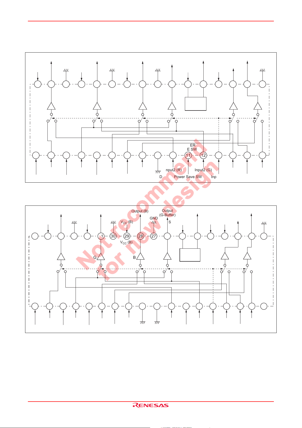
Block Diagram
M61323SP
Sync-Sep. OUT
22
Sync-Sep.
POWER
SAVE SW
V
CC
V
CC
V
CC
Output (R)
(R)
GND
V
CC
Output (G)
(G)
GND
Output (B)
VCC (B)
GND
Output
(G-Buffer)
Sync-Sep. INPUT
23
VCC (R) VCC (G) VCC (B)
RBG V
V
(R) VCC (G) VCC (B)
CC
Input1 (R)
VCC (R)
VCC (G)
Input1 (G)
VCC (B)
Input1 (B)
Input1 (V)
Input1 (H)
G
GND
Input2 (R) Input2 (G) Input2 (B)
GND
Power Save SW Input SW
M61323FP
Output (H)
1921 202425262728293132 30
H
141312111098654321 7
Output (V)
18
15 16
Input2 (H)
GND
17
Input2 (V)
V
CC
Output (G)
(G)
Output (R)
V
(R)
CC
VCC (R) VCC (G) VCC (B)
NC
GND
RBGG V
(R) VCC (G) VCC (B)
V
CC
Input
1 (R)
VCC (R)
Input
1 (G)
(G)
V
CC
Input
1 (B)
(B)
V
CC
GND
Input
1 (H)
V
CC
Input
Output (B)
(B)
1 (V)
GND
GND
GND
GND
Output
(G-Buffer)
Sync-Sep. INPUT
26
Input
2 (R)
Power Save SW
Sync-Sep. OUT
Sync-Sep.
POWER
SAVE SW
Input
2 (G)
V
CC
2325 24272829303132333536 34
V
CC
Input
141312111098654321 7
H
Input
SW
Output (H)
V
CC
22
V
CC
15 16
2 (B)
Input
21
2 (H)
Output (V)
Input
2 (V)
GND
1920
NCGND
1817
REJ03F0201-0201 Rev.2.01 Mar 31, 2008
Page 2 of 19
Page 3
M61323SP/FP
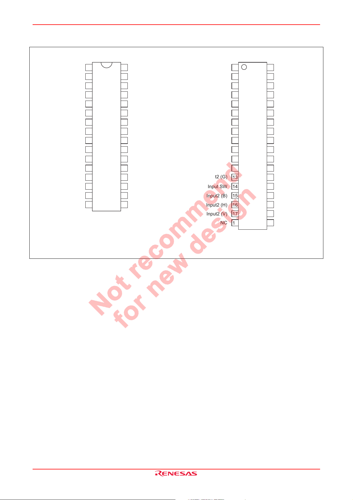
Pin Arrangement
V
1 (R)
CC
Input1 (R)
VCC1 (G)
Input1 (G)
1 (B)
V
CC
Input1 (B)
Input1 (H)
Input1 (V)
GND1
Input2 (R)
Power Save SW
Input2 (G)
Input SW
Input2 (B)
Input2 (H)
Input2 (V)
M61323SP
1
2
3
4
5
6
7
8
9
10
11
12
13
14
15
16
(Top view)
VCC2 (R)
32
31
Output (R)
30
GND2 (R)
V
29
CC
28
Output (G)
GND2 (G)
27
26
V
CC
Output (B)
25
GND2 (B)
24
G Buffer out
23
Sync SEP in
22
Sync SEP out
21
V
20
CC
Output (H)
19
18
Output (V)
GND3
17
2 (G)
2 (B)
3
V
1 (R)
CC
Input1 (R)
VCC1 (G)
Input1 (G)
1 (B)
V
CC
Input1 (B)
Input1 (H)
Input1 (V)
GND1
GND1
Input2 (R)
Power Save SW
Input2 (G)
Input SW
Input2 (B)
Input2 (H)
Input2 (V)
NC
M61323FP
1
2
3
4
5
6
7
8
9
10
11
12
13
14
15
16
17
18
36
NC
35
V
CC
34
Output (R)
33
GND2 (R)
V
32
CC
31
Output (G)
30
GND2 (G)
29
VCC2 (B)
28
Output (B)
27
GND2 (B)
G Buffer out
26
Sync SEP in
25
Sync SEP out
24
V
23
CC
V
22
CC
21
Output (H)
20
Output (V)
19
GND3
2 (R)
2 (G)
3
3
Outline: PRDP0032BA-A (32P4B)
(Top view)
Outline: PRSP0036GA-B (36P2R-D)
REJ03F0201-0201 Rev.2.01 Mar 31, 2008
Page 3 of 19
Page 4
M61323SP/FP
Absolute Maximum Ratings
(Ta = 25°C)
Item Symbol Ratings Unit
Supply voltage VCC 7.0 V
Power dissipation Pd 1603 (SP), 1068 (FP) mW
Operating temperature Topr −20 to +85 (SP), −20 to +75 (FP) °C
Storage temperature Tstg −40 to +150 °C
Electrostatic discharge Surge ±200 V
Recommended supply voltage Vopr 5.0 V
Recommended supply voltage range Vopr' 4.75 to 5.25 V
Electrical Characteristics
(M61323SP VCC = 5.0 V, Ta = 25°C)
mA
V
V
dB
dB
dB
dB
dB
dB
Test
Point
SW2
SW4
SW6
SW7
SW8
SW10
SW12
SW14
(s)
Rin1
Gin1
Bin1
Hin1
Vin1
Rin2
Gin2
bb
bb bbbb bbb b
31
V
28
25
V
28
25
23
V
V
P-P
28
25
P-P
31
28
25
31
28
25
28
25
23
bb bbbb bbb b
b
b
bb bbbb bbb
bb bbbb bbb b
b
b
bb bb
abb
bab
bba
SG1
SG1
b
bb bb
abb
bab
SG2
SG2
a
b
SG2
bb bbb b
b
SG1
bba
b a
SG2
Relative to measured values above
Relative to measured values above
bbb b b bbb b
b a
bbbbb
bbbb bb b
abb
bab
SG1
SG1
bbbb bb b
abb
SG2
bab
SG2
a
SG2
bbbb b b
SW15
Bin2
Hin2
bba
SG1
bba
bb a
SG2
bb
SW16
Vin2
b
SW22
Sync
b
b
b
b
b
b
b
SW11
P.sav
a
3 V
a
3 V
a
3 V a3 V
3 V
a
3 V a3 V
a
3 V
a
3 V a3 V
3 V
a
3 V
3 V
a
3 V
SW13
Switch
b
3 V
3 V
Item
Circuit current1
Circuit current2
RGB SW
Output DC voltage1
Output DC voltage2
Output DC voltage3
Output DC voltage4
Maximum allowable
input level1
Maximum allowable
input level2
Voltage gain1
Relative voltage gain1
Voltage gain2
Relative voltage gain2
Voltage gain3
Voltage gain4
Symbol
I
CC
ICCSTBY
Vdc1
Vdc2
Vdc3
Vdc4
Vimax1
Vimax2
G
V1
∆G
V1
G
V2
∆G
V2
G
V3
G
V4
Limits Input SW
Min.
Typ. Max. Unit
70 mA b b b b b b b b b
b bb
−0.1 0.7 1.3
−0.4 0 0.4
−0.1 0.7 1.3 31
−0.4 0 0.4
−0.6 0 0.6
−0.6 0 0.6 23 b a
10
1.5 b
1.5 31
0.9 a
0.9 23
1.8 31
1.8 b
REJ03F0201-0201 Rev.2.01 Mar 31, 2008
Page 4 of 19
Page 5

M61323SP/FP
Electrical Characteristics (cont.)
Item
Freq. characteristic1
(100 MHz)
Relative
Freq.characteristic1
(100 MHz)
Freq.characteristic2
(100 MHz)
Relative
Freq.characteristic2
(100 MHz)
Freq.characteristic3
(250 MHz)
Freq.characteristic4
(250 MHz)
Crosstalk between
two inputs1 (10 MHz)
Crosstalk between
two inputs2 (10 MHz)
Crosstalk between
two inputs3 (100 MHz)
Crosstalk between
two inputs4 (100 MHz)
Crosstalk between
channels1 (10 MHz)
Crosstalk between
channels2 (10 MHz)
Crosstalk between
channels3 (100 MHz)
Crosstalk between
channels4 (100 MHz)
Pulse characteristic1
Pulse characteristic2
Symbol
F
C1
∆F
C1
F
C2
∆F
C2
F
C3
F
C4
C.T.I.1
C.T.I.2
C.T.I.3
C.T.I.4
C.T.C1
C.T.C2
C.T.C3
C.T.C4
Tr1
Tf1
Tr2
Tf2
Limits Input SW
Min.
Typ. Max.
−10 1
−10 1
0
−11 31
−10 1
bb a
−3
−3 bb a
−60 −45
−60 −45
−40 −30
−40 −30
−50 −40
−50 −40
−30 −25
−30 −25
1.6 2.5
1.6 2.5
Unit
dB
dB
dB
dB
dB
dB
dB
dB
dB
dB
dB
dB
dB
dB
ns
ns 1.6 2.5 b b b b b b b b31
ns
ns 1.6 2.5 bbb b b b31
Test
Point
SW2
SW4
SW6
SW7
SW8
SW10
SW12
SW14
(s)
Rin1
Gin1
Bin1
Hin1
Vin1
Rin2
abb
SG4
SG5
abb
SG3
abb
SG4
abb
SG3
abb
SG4
abb
SG6
abb
SG6
Gin2
bab
SG4
bab
SG5
bab
SG3
bab
SG4
bab
SG3
bab
SG4
bab
SG6
bab
SG6
abb
bab
31
SG4
28
25
bbb a
28
25
31
28
SG5
25
31
28
25
31
abb
28
SG3
25
31
28
25
31
abb
28
SG4
25
31
28
25
31
abb
28
SG3
25
31
28
25
31
abb
28
SG4
25
31
28
25
abb
31
SG6
28
25
abb
SG6
28
25
31
28
25
28
25
SG4
bab
SG5
bab
SG3
bab
SG4
bab
SG3
bab
SG4
bab
SG6
bab
SG6
bba
SG4
bba
SG5
bba
SG3
bba
SG4
bba
SG3
bba
SG4
bba
SG6
bba
SG6
bb b b bb a
bb
Relative to measured values above
Relative to measured values above
bb b bbb babb
b a
bb b bbbb
bbbbbbb
bbbbbbbb
bbbbbbbb
bbbbbbbb
Bin2
bba
SG4
bba
SG5
bba
SG3
bba
SG4
bba
SG3
bba
SG4
bba
SG6
bba
SG6
SW15
Hin2
bbbb b b b
bbbb b b b
bbbb b b b
bbbb b b b
bbb b b b
SW22
SW16
Sync
Vin2
bbb bb
bbb bb babb
b a
b a
b a
b a
b a
bb a
bb a
SW11
P.sav
3 V
a
3 V
3 V
a
3 V
a
3 V
3 V
a
3 V
3 V
a
3 V
a
3 V
a
3 V
a
3 V
a
3 V
a
3 V
a
3 V
a
3 V
SW13
Switch
b
3 V
3 V
3 V
b
3 V
b
b
3 V
b
3 V
b
b
3 V
3 V
REJ03F0201-0201 Rev.2.01 Mar 31, 2008
Page 5 of 19
Page 6

M61323SP/FP
Electrical Characteristics (cont.)
Item
Symbol
Min.
HV SW
High level
output voltage1
High level
output voltage2
Low level
output voltage1
Low level
output voltage2
Input threshold
voltage H
Input threshold
voltage L
Rising time3
Falling time3
Rising delay time
Falling delay time
Vdch1
Vdch2
Vdcl1
Vdcl2
VithH
VithL
Tr3
Tf3
HVDr
HVDf
0.2 0.5
1.8 2.0 2.2
1.0 1.4 1.6
25
40 60
Sync SEP.
Sync on G input
minimum voltage
Sync output
high level voltage
Sync output
low level voltage
Sync output
rising time 3
Sync output
falling time 3
Sync output
rising delay time
Sync output
falling delay time
SYrv
SYVH
SYVL
STr
STf
SDr
SDf
bbbbb b 21 a
bbbbb b 21 a
bbbbb b 21 a
Channel Select SW, Power Save SW
Channel select SW
threshold voltage1
Channel select SW
threshold voltage2
Power save SW
threshold voltage1
Power save SW
threshold voltage2
Vthch1
Vthch2
VthPH
VthPL
VV
2.0
Limits Input SW
Typ. Max. Unit
3.8 4.2 b b b b b b a
0.2 0.5
a
15 ns a
40 60 ns a
bbbbb b 21 a
4.3 b b bbb b 21 a
15
40 b b bbb b 21 a
40 60
2.5
1.0
a
1.0 a
Test
Point
SW2
SW4
SW6
SW7
SW8
SW10
SW12
SW14
SW15
(s)
Rin1
Gin1
Bin1
Hin1
Vin1
Rin2
Gin2
Bin2
18
V
V3.8 4.2 b b bbb b a
V
V
V a
V a
ns
ns
V
P-P
V a
V a
ns a
ns a
ns a
ns a
V
V
bb b
19
18
bb b a
19
18
19
18
bb b b b
19
18
19
bb b
18
19
18
19
bb b
18
19
bb b
18
19
bb b
18
19
SG6 aSG6
SG6 aSG6
a
SG6aSG6aSG6
b a
SG6aSG6aSG6 aSG8 aSG8
a
SG6
a
SG6
a
SG8
SG8
a
SG8 aSG8
SG8 aSG8
SG8 aSG8
SG8 aSG8
SG8 aSG8
a
SG8 aSG8
SG8 aSG8
a
a
SG8
SG8
a
a
SG8
SG8
SG8 aSG8
bbb
bbb
bbb
bbb
bbb
bbbbb
bbb
bbb
bbbbb b 21 a
bbb a
bbb a
bbbbb
bbbbb
SW16
Hin2
Vin2
a
SG8
SG8
bbbbb b
a
SG8 aSG8
bbbbb b
bb
bb
bb
bbb
b b0.2 b b
bb3.8 b b
bb0.50.2 b b
bb25 b b
bb bb
bb60 bb
bbbb
bb
bb
SW22
Sync
b
b a
bbb b
b a
b
a
SG7
SG7
SG7
SG7
SG7
SG7
SG7
a
SG7
a
SG7
a
SG7
SG7
SW11
P.sav
a
3 V
3 V
a
3 V
a
3 V
a
3 V
3 V
a
3 V
3 V
a
3 V
a
3 V
3 V
3 V
3 V
3 V
3 V
3 V
3 V
a
3 V
a
3 V
a
variable
a
variable
SW13
Switch
b
a
3 V
b
a
3 V
b
b
b
b
b
b
a
variable
a
variable
b
REJ03F0201-0201 Rev.2.01 Mar 31, 2008
Page 6 of 19
Page 7

M61323SP/FP
Electrical Characteristics Test Method (M61323SP)
Circuit Current 1
No signal. Measure the total circuit current as I
when supplying 3 VDC to pin 11.
CC
Circuit Current 2
No signal. Measure the total circuit current as I
STBY when pin 11 connected to GND.
CC
Output DC Voltage 1, 2
Set SW13 to GND (or OPEN), measure the DC voltage of TP31 (TP28, TP25) when there is no signal input.
The DC voltage is as vdc1 (vdc2).
Output DC Voltage 3, 4
Measure the DC voltage TP23 same as "Output DC voltage 1, 2". The DC voltage is Vdc3 (Vdc4).
Maximum Allowable Input Level 1, 2
Set SW13 to GND, input SG1 to pin 2 only. Gradually increasing the SG1 amplitude, read the amplitude of the input
signal when the output waveform of TP31 is strained. The value is as Vimax1. In the same way, measure Vimax1 in
response to inputs in pin 4 and pin 6 only.
Then set SW13 to OPEN, measure Vimax2 in response to inputs in pin 10, 12 and 14 only.
Voltage Gain 1, 2
1. The conditions is as table.
2. Set SW13 to GND, input SG2 (0.7 V
3. Voltage gain G
GV1 = 20log (dB)
4. In the same way, calculate G
is
V1
VOR1 [V
0.7
]
P-P
in response to inputs in pin 4 and pin 6 only.
V1
5. Then set SW13 to OPEN, measure G
) to pin 2 only. Read the output amplitude of TP31. The value is as VOR1.
P-P
in response to inputs in pin l0, 12 and 14 only.
V2
Relative Voltage Gain 1, 2
1. Calculate relative voltage gain ∆G
∆G
= GV1R − GV1G, GV1G − GV1B, GV1B − GV1R
V1
2. In the same way, calculate ∆G
1 by the following formula.
V
V2
Voltage Gain 3, 4
1. The conditions is as table.
2. Read the output amplitude of TP23.
3. Calculate G
, GV4 same as "Voltage gain 1".
V3
Freq. Characteristic 1, 2/Relative Freq. Characteristic 1, 2
1. The conditions is as table. This measurement shall use active probe.
2. Set SW13 to GND, input SG4 (0.7 V
In the same way, input SG2 (0.7 V
3. Freq.characteristic1 F
FC1 = 20log (dB)
4. In the same way, calculate F
C1
VOR2 [V
V
1 [V
OR
is
]
P-P
]
P-P
in response to inputs in pin 4 and pin 6 only.
C1
) to pin 2 only. Measure TP31 output amplitude as VOR1.
P-P
) to pin 2 only. Measure TP31 output amplitude as VOR2.
P-P
5. The difference between of each channel Freq.characteristic is as ∆F
6. Then set SW13 to OPEN, measure F
and ∆FC2 in response to inputs in pin 10, 12 and 14 only.
C2
.
C1
REJ03F0201-0201 Rev.2.01 Mar 31, 2008
Page 7 of 19
Page 8

M61323SP/FP
Freq. Characteristic 3, 4
Measure the F
, FC4 when SG5 of input signal. (For reference)
C3
Crosstalk between Two Inputs 1, 2
1. The conditions is as table. This measurement shall use active probe.
2. Set SW13 to GND, input SG3 to pin 2 only. Read the output amplitude of TP31. The value is as V
3. Then set SW13 to OPEN, read the output amplitude of TP31. The value is as V
OR
3'.
OR
3.
4. Crosstalk between two inputs 1 C.T.I.1 is
C.T.I.1 = 20log (dB)
VOR3' [V
V
OR
3 [V
P-P
P-P
]
]
5. In the same way, calculate C.T.I.1 in response to inputs in pin 4 and pin 6 only.
6. Then set SW13 to OPEN, input SG2 to pin 10 only. Read the output amplitude of TP31. The value is as V
7. Set SW13 to GND, read the output amplitude of TP31. The value is as V
OR
4'.
8. Crosstalk between two inputs 1 C.T.I.2 is
C.T.I.2 = 20log (dB)
VOR4' [V
V
OR
4 [V
P-P
P-P
]
]
9. In the same way, calculate C.T.I.2 in response to inputs in pin 12 and pin 14 only.
Crosstalk between Two Inputs 3, 4
Set SG4 as the input signal, and then the same method as table, measure C.T.I.3, C.T.I.4.
Crosstalk between Channels 1, 2
OR
4.
1. The conditions is as table. This measurement shall use active probe.
2. Set SW13 to GND, input SG3 (0.7 V
3. Next, measure TP28, TP25 in the same state, and the amplitude is as V
) to pin 2 only. Read the output amplitude of TP31. The value is as VOR5.
P-P
5, VOB5.
OG
4. Crosstalk between channels1 C.T.C1 is
C.T.C1 = 20log (dB)
VOG5 or VOB5
V
5
OR
5. In the same way, calculate C.T.C1 in response to inputs in pin 4 and pin 6 only.
6. Then set SW13 to OPEN, input SG3 (0.7 V
Read the output amplitude of TP31. The value is as V
7. Next, measure TP28, TP25 in the same state, and the amplitude is as V
) to pin 10 only.
P-P
OR
6.
6, VOB6.
OG
8. Crosstalk between two inputs 1 C.T.C2 is
C.T.C2 = 20log (dB)
VOG6 or VOB6
V
6
OR
9. In the same way, calculate C.T.C2 in response to inputs in pin 9 and pin 11 only.
Crosstalk between Channels 3, 4
Set SG4 as the input signal, and then the same method astable, measure C.T.C3, C.T.C4.
REJ03F0201-0201 Rev.2.01 Mar 31, 2008
Page 8 of 19
Page 9

M61323SP/FP
Pulse Characteristic 1, 2
1. The conditions is as table (SG5 amplitude 0.7 V
). Set SW13 to GND (or OPEN).
P-P
2. Measure rising Tri and falling Tfi for 10% to 90% of the input pulse with active probe.
3. Next, measure rising Tro and falling Tfo for 10% to 90% of the output pulse with active probe.
4. Pulse characteristic Tr1, Tf1 (Tr2, Tf2) is
100%
Tr1 (Tr2) = √ (Tro)2 − (Tri)2 (ns)
Tf1 (Tf2) = √ (Tfo)2 − (Tfi)2 (ns)
0%
Tr Tf
90%
10%
<HV-SW>
High Level Output Voltage 1, 2/Low Level Output Voltage 1, 2
1. The conditions is as table. Input SG8 to pin 7 (or pin 8). Set SW13 to GND, read the output high level and low
voltage of TP19, TP18. The value is as Vdch1, Vdcl1.
2. Input SG8 to pin 15 (or pin 16). Set SW13 to OPEN, read the output high level and low voltage of TP19, TP18.
The value is as Vdch2, Vdcl2.
Input Threshold Voltage H/Input Threshold Voltage L
1. Set SW13 to GND (or OPEN). Gradually increasing the voltage of pin 7 (or pin 15) from 0 V, measure the input
voltage of pin 7 (or pin 15) when the TP19 voltage turned high level (3.8 V or more). The value is as VithH.
2. Gradually decreasing the voltage of pin 7 (or pin 15) from 3 V, measure the input voltage of pin 7 (or pin 15) when
the TP19 voltage turned low level (0.5 V or less). The value is as VithL.
3. In the same way, measure the input voltage of pin 8 (or pin 16) as VithH, VithL.
Rising Time/Falling Time
1. The conditions is as table. This measurement shall use active probe.
2. Measure rising Tri and falling Tfi for 20% to 80% of the output pulse as Tr3, Tf3 (Tr4, Tf4).
100%
0%
Tr' Tf'
80%
20%
Rising Delay Time/Falling Delay Time
Set SW13 to GND (or OPEN), input SG8 to pin 7 (or pin 15).
Measure the rising delay time HVDr and the falling delay time HVDf.
In the same way, measure HVDr and HVDf when input SG8 to pin 8 (or pin 16)
SG8
HVDr HVDf
50%
Waveform output
REJ03F0201-0201 Rev.2.01 Mar 31, 2008
Page 9 of 19
50%
Page 10

M61323SP/FP
<Sync-Separation>
Sync Input Minimum Voltage
Gradually decreasing the amplitude of SG7 in pin 22, measure the amplitude of SG7 when the Sync-Sep output signal
turn off. The value is as SYrv.
Sync Output High Level Voltage/Sync Output Low Level Voltage
Input SG7 to pin 22, read the output high level and low voltage of TP21. The value is as SYVH, SYVL.
Sync Output Rising Time/Sync Output Falling Time
1. The conditions is as table. (SG7 amplitude 0.3 V
P-P
)
This measurement shall use active probe.
2. Measure rising Tri and falling Tfi for 10% to 90% of the input pulse as STr, STf.
100%
0%
STr STf
90%
10%
Sync Output Rising Delay Time/Sync Output Falling Delay Time
Input SG7 to pin 22. Measure the rising delay time SDr and the falling delay time SDf.
SG7
SDr SDf
Waveform output
50%
50%
<Others>
Channel Select SW Threshold 1, 2
1. Gradually increasing the voltage of pin 13 from 0 V, measure the maximum voltage of pin 13 when the channel 1 is
selected. The value is as Vthch1.
2. Gradually decreasing the voltage of pin 13 from 5 V, measure the minimum voltage of pin 13 when the channel 2 is
selected. The value is as Vthch2.
Power Save SW Threshold 1, 2
1. Gradually increasing the voltage of pin 11 from 0 V, measure the maximum voltage of pin 11 when the power save
mode. The value is as VthPL.
2. Gradually decreasing the voltage of pin 13 from 5 V, measure the minimum voltage of pin 11 when the power save
mode. The value is as VthPH.
REJ03F0201-0201 Rev.2.01 Mar 31, 2008
Page 10 of 19
Page 11

M61323SP/FP
Input Signal
SG No. Signals
SG1 Sine wave (f = 60 kHz, 0.7 V
SG2 Sine wave (f = 1 MHz, 0.7 V
SG3 Sine wave (f = 10 MHz, 0.7 V
SG4 Sine wave (f = 100 MHz, 0.7 V
SG5 Sine wave (f = 250 MHz, 0.7 V
SG6
SG7 Sync (fH = 60 kHz)
(Amplitude variable) )
P-P
(Amplitude variable) )
P-P
(Amplitude variable) )
P-P
(Amplitude variable) )
P-P
(Amplitude variable) )
P-P
0.7 V
P-P
(variable)
0.7 V
P-P
Amplitude variable
(Typ. = 0.3 V
P-P
DUTY 80%
fH = 60 kHz
0.7 V
P-P
)
SG8
TTL
Typical Characteristics
Thermal Derating (M61323SP)
1750
1603
1500
1250
1000
833
750
500
Power Dissipation Pd (mW)
250
4.5 µs
Thermal Derating (M61323FP)
1750
1500
1250
1068
1000
750
640
500
Power Dissipation Pd (mW)
250
5 V
0 V
DUTY 50%
fH = 60 kHz
0
−25 0 25 50 75 100 125 150 −25 0 25 50 75 100 125 150
85
Ambient Temperature Ta (°C)
REJ03F0201-0201 Rev.2.01 Mar 31, 2008
Page 11 of 19
0
Ambient Temperature Ta (°C)
Page 12

M61323SP/FP
Test Circuit (M61323SP)
VCCB
5 V
SW B
a b
V
CC
a
b
A
SW A
A 5 V
0.01 µ
+
47 µ
A
0.01 µ
+
47 µ
R-OUT
R-SW
+
47 µ
ab
SW32
ab
SW29
TP31
+
0.01 µ
47 µ
G-OUT
V
CC
V
CC
G-SW
V
CC
0.01 µ
75
SW2
V
CC
+
47 µ
0.01 µ
+
0.01 µ
75
SW4
ab ab
ab
TP23
SG
SS
ab
SW22
ab
SW26
TP28 TP25 TP21
1 µ
+
+
0.01 µ
47 µ
0.01 µ
B-OUT
V
CC
B-SW
V
CC
ECO-SW
TP11
0.01 µ0.01 µ
SW11
SW13
c
b
a
open
+
47 µ
75
SW6
47 µ
0.01 µ
SW7
SW8
a b
a b
0.01 µ
75
SW10
a b
+
47 µ
0.01 µ
75
SW12
a b
TP13
+
0.01 µ
V
CC
a
open
47 µ
SW14
b
75
+
47 µ
TP19
1922 21 20232425262728293132 30 1718
c
0.01 µ
a b
TP18
15 16141312111098654321 7
+
47 µ
SW15
ab
VCCC 5 V
SW C
ab
A
SW16
ab
SG
RGB
SG
HV
Units Resistance: Ω
Capacitance: F
REJ03F0201-0201 Rev.2.01 Mar 31, 2008
Page 12 of 19
Page 13

M61323SP/FP
Application Example (M61323SP)
V
CC
5 V
0.01 µ+47 µ
V
CC
5 V
0.01 µ+47 µ
INPUT1
Rin1
Gin1
Bin1
Hin1
Vin1
+
0.01 µ
47 µ
V
CC
RBGVH
V
CC
(5 V)
0.01 µ 0.01 µ 0.01 µ
75
V
CC
(5 V)
+
47 µ
0.01 µ
+
47 µ
0.01 µ
V
CC
+
47 µ
0.01 µ
V
CC
1 µ
+
2325 24272829303132 26
22
G
V
CC
(5 V)
+
47 µ
0.01 µ
75
+
47 µ
0.01 µ
75
0.01 µ
75
Power save
SW
+
47 µ
Sync
Sepa
0.01 µ
75
21
OUTPUT
R
OUT
G
OUT
B
OUT
G Buffer
OUT
Sync SEP
OUT
Hout Vout
V
CC
5 V
0.01 µ47 µ
CC
V
CC
1920 18 17
+
POWER SAVE V
(H-SW, V-SW,
G-Buffer, Sync-SEP)
15 16141312111098654321 7
0 to 0.8 V : INPUT1
2.0 to 5.0 V: INPUT2
+
47 µ
+
47 µ
0.01 µ
75
PowerSave V
CC
INPUT2
Rin2
Gin2
Bin2
Hin2
Vin2
Units Resistance: Ω
Capacitance: F
REJ03F0201-0201 Rev.2.01 Mar 31, 2008
Page 13 of 19
Page 14

M61323SP/FP
Pin Description (M61323SP)
pin No. Name DC Voltage (V) Peripheral Circuit Function
1
3
5
20
26
29
32
2
4
6
10
12
14
(R)
V
CC
(G)
V
CC
(B)
V
CC
(H, V,
V
CC
Sync-Sep.)
(ROUT)
V
CC
(GOUT)
V
CC
(BOUT)
V
CC
Input1 (R)
Input1 (G)
Input1 (B)
Input2 (R)
Input2 (G)
Input2 (B)
5.0
5.0
2.3
750
643
2.48 V
2.2 mA
Input signal with low impedance
3 V
7
8
15
16
9
17
24
27
30
Input1 (H)
Input1 (V)
Input2 (H)
Input2 (V)
GND (V-SW)
GND
(H, V, Sync-
Sep.)
GND (B-out)
GND (G-out)
GND (R-out)
500
7 k
SW
GND
Input pulse between 3 V and 5 V
3 to 5 V
0 to 0.8 V
REJ03F0201-0201 Rev.2.01 Mar 31, 2008
Page 14 of 19
Page 15

M61323SP/FP
Pin Description (M61323SP) (cont.)
pin No. Name DC Voltage (V) Peripheral Circuit Function
11 PwrSave-SW 2.5
30 k 15 k 25 k
2.0 V
Do not apply more 5 V DC
voltage
10 k
13 CONT-SW 2.4
18
19
Vout
Hout
20 k
26 k
2.4 V
15 k
20 k 20 k
15 k
5 k
20 k
25 k
Do not apply more 5 V DC
voltage
7.3 k24 k
100
15 k
REJ03F0201-0201 Rev.2.01 Mar 31, 2008
Page 15 of 19
Page 16

M61323SP/FP
Pin Description (M61323SP) (cont.)
pin No. Name DC Voltage (V) Peripheral Circuit Function
21 Sync sep OUT
15 k
22 Sync sep IN
23 G Buffer OUT
15 k
15 k
CLAMPref
10 k
10 k
100
Connect a capacitance
between the pin and GND
when not use SYNC-SEP
2 k
Vth
5 k5 k
2 k
25
28
31
Video OUT (B)
Video OUT (G)
Video OUT (R)
1.5
32, 29, 26 pin
50
30, 27, 24 pin
31, 28, 25 pin
REJ03F0201-0201 Rev.2.01 Mar 31, 2008
Page 16 of 19
Page 17

M61323SP/FP
Note How to Use This IC (M61323SP)
1. R, G, B input signal is 0.7 V
of standard video signal.
P-P
2. H, V input is 5.0 V TTL type.
3. Input signal with sufficient low impedance to input terminal.
4. The terminal of R, G, B output pin are shown as figure 1.
When resistance is connected between the pin 31 (28, 25) and GND, I
will be increase.
CC
5. Switch (pin 13) can be changed by supplying some voltage as figure 2.
0 to 0.5 V: INPUT1
2.5 to 5 V: INPUT2
Do not apply V
6. Power save mode is provided for saving I
or more DC voltage.
CC
less than about 10 mA as figure 3.
CC
0 to 0.5 V: Power save mode (H.V-SW, Sync-Sep., G-Buffer)
2.5 to 5 V: Normal mode
Do not apply 5 V or more DC voltage
7. When not use the Sync-separation circuit built in this IC, capacitance of several tens of pF is required between the
pin 22 and GND.
5 V
I < 5 mA
50 Ω
R
600 Ω
Figure 1
13
Figure 2
11
Figure 3
REJ03F0201-0201 Rev.2.01 Mar 31, 2008
Page 17 of 19
Page 18

M61323SP/FP
Cautions for Manufacturing Boards
Built-in wide band preamplifier may cause oscillation due to the wiring shape on the board.
Be careful for the following points.
• V
shall use a stable power supply.
CC
(Individual V
should use an independent power supply.)
CC
• GND should be as wide as possible. Basically, solid earth should be used.
Make the load capacitance of output pins as small as possible.
• Also ground the hold capacitance to stable GND, which is as near to the pin as possible.
• Insertion of a resistance of several tens of ohms between the output pin and the circuit at the next stage makes
oscillation harder.
• When inserting an output pull-down resistance, make wire between the output pin and the resistance as short as
possible.
REJ03F0201-0201 Rev.2.01 Mar 31, 2008
Page 18 of 19
Page 19

M61323SP/FP
Package Dimensions
P-SDIP32-8.9x28-1.78 2.2g
32
1
*2
D
A
L
SEATING PLANE
e
32P4BPRDP0032BA-A
*3 *3
b
3
b
p
RENESAS CodeJEITA Package Code Previous Code
P-SSOP36-8.4x15-0.80 0.5g
RENESAS CodeJEITA Package Code Previous Code
36P2R-DPRSP0036GA-B
MASS[Typ.]
17
16
b
2
MASS[Typ.]
E
*1
2
A
1
A
1
e
c
NOTE)
1. DIMENSIONS "*1" AND "*2"
DO NOT INCLUDE MOLD FLASH.
2.
DIMENSION "*3" DOES NOT
INCLUDE TRIM OFFSET.
Dimension in Millimeters
Reference
Symbol
Min Nom Max
e
1
D
E
A
A
A
b
p
b
2
b
3
c
e
L
10.169.86 10.46
27.8 28.0 28.2
8.9
8.75
1
0.51
2
3.8
0.35 0.45 0.55
0.63 0.73 1.03
0.9 1.0 1.3
0.22 0.27 0.34
0°
1.778
1.528 2.028
3.0
9.05
5.08
15°
1936
E
E
H
*1
1
Index mark
*2
D
A
y
e
18
*3
b
p
c
A
2
Detail F
F
NOTE)
1. DIMENSIONS "*1" AND "*2"
DO NOT INCLUDE MOLD FLASH.
2.
DIMENSION "*3" DOES NOT
INCLUDE TRIM OFFSET.
Dimension in Millimeters
Reference
A
1
L
Symbol
Min Nom Max
D
14.8 15.0 15.2
E
8.2 8.4 8.6
A
2
A
A
0
1
b
0.3 0.35 0.45
p
c
0.18 0.2 0.25
0° 8°
H
E
11.63 11.93 12.23
e
0.65 0.95
y
L
0.3 0.5 0.7
2.05
0.1 0.2
0.8
2.35
0.10
REJ03F0201-0201 Rev.2.01 Mar 31, 2008
Page 19 of 19
Page 20

Sales Strategic Planning Div. Nippon Bldg., 2-6-2, Ohte-machi, Chiyoda-ku, Tokyo 100-0004, Japan
Notes:
1. This document is provided for reference purposes only so that Renesas customers may select the appropriate Renesas products for their use. Renesas neither makes
warranties or representations with respect to the accuracy or completeness of the information contained in this document nor grants any license to any intellectual property
rights or any other rights of Renesas or any third party with respect to the information in this document.
2. Renesas shall have no liability for damages or infringement of any intellectual property or other rights arising out of the use of any information in this document, including,
but not limited to, product data, diagrams, charts, programs, algorithms, and application circuit examples.
3. You should not use the products or the technology described in this document for the purpose of military applications such as the development of weapons of mass
destruction or for the purpose of any other military use. When exporting the products or technology described herein, you should follow the applicable export control laws
and regulations, and procedures required by such laws and regulations.
4. All information included in this document such as product data, diagrams, charts, programs, algorithms, and application circuit examples, is current as of the date this
document is issued. Such information, however, is subject to change without any prior notice. Before purchasing or using any Renesas products listed in this document,
please confirm the latest product information with a Renesas sales office. Also, please pay regular and careful attention to additional and different information to be
disclosed by Renesas such as that disclosed through our website. (http://www.renesas.com )
5. Renesas has used reasonable care in compiling the information included in this document, but Renesas assumes no liability whatsoever for any damages incurred as a
result of errors or omissions in the information included in this document.
6. When using or otherwise relying on the information in this document, you should evaluate the information in light of the total system before deciding about the applicability
of such information to the intended application. Renesas makes no representations, warranties or guaranties regarding the suitability of its products for any particular
application and specifically disclaims any liability arising out of the application and use of the information in this document or Renesas products.
7. With the exception of products specified by Renesas as suitable for automobile applications, Renesas products are not designed, manufactured or tested for applications
or otherwise in systems the failure or malfunction of which may cause a direct threat to human life or create a risk of human injury or which require especially high quality
and reliability such as safety systems, or equipment or systems for transportation and traffic, healthcare, combustion control, aerospace and aeronautics, nuclear power, or
undersea communication transmission. If you are considering the use of our products for such purposes, please contact a Renesas sales office beforehand. Renesas shall
have no liability for damages arising out of the uses set forth above.
8. Notwithstanding the preceding paragraph, you should not use Renesas products for the purposes listed below:
(1) artificial life support devices or systems
(2) surgical implantations
(3) healthcare intervention (e.g., excision, administration of medication, etc.)
(4) any other purposes that pose a direct threat to human life
Renesas shall have no liability for damages arising out of the uses set forth in the above and purchasers who elect to use Renesas products in any of the foregoing
applications shall indemnify and hold harmless Renesas Technology Corp., its affiliated companies and their officers, directors, and employees against any and all
damages arising out of such applications.
9. You should use the products described herein within the range specified by Renesas, especially with respect to the maximum rating, operating supply voltage range,
movement power voltage range, heat radiation characteristics, installation and other product characteristics. Renesas shall have no liability for malfunctions or damages
arising out of the use of Renesas products beyond such specified ranges.
10. Although Renesas endeavors to improve the quality and reliability of its products, IC products have specific characteristics such as the occurrence of failure at a certain
rate and malfunctions under certain use conditions. Please be sure to implement safety measures to guard against the possibility of physical injury, and injury or damage
caused by fire in the event of the failure of a Renesas product, such as safety design for hardware and software including but not limited to redundancy, fire control and
malfunction prevention, appropriate treatment for aging degradation or any other applicable measures. Among others, since the evaluation of microcomputer software
alone is very difficult, please evaluate the safety of the final products or system manufactured by you.
11. In case Renesas products listed in this document are detached from the products to which the Renesas products are attached or affixed, the risk of accident such as
swallowing by infants and small children is very high. You should implement safety measures so that Renesas products may not be easily detached from your products.
Renesas shall have no liability for damages arising out of such detachment.
12. This document may not be reproduced or duplicated, in any form, in whole or in part, without prior written approval from Renesas.
13. Please contact a Renesas sales office if you have any questions regarding the information contained in this document, Renesas semiconductor products, or if you have
any other inquiries.
RENESAS SALES OFFICES
http://www.renesas.com
Refer to "http://www.renesas.com/en/network" for the latest and detailed information.
Renesas Technology America, Inc.
450 Holger Way, San Jose, CA 95134-1368, U.S.A
Tel: <1> (408) 382-7500, Fax: <1> (408) 382-7501
Renesas Technology Europe Limited
Dukes Meadow, Millboard Road, Bourne End, Buckinghamshire, SL8 5FH, U.K.
Tel: <44> (1628) 585-100, Fax: <44> (1628) 585-900
Renesas Technology (Shanghai) Co., Ltd.
Unit 204, 205, AZIACenter, No.1233 Lujiazui Ring Rd, Pudong District, Shanghai, China 200120
Tel: <86> (21) 5877-1818, Fax: <86> (21) 6887-7858/7898
Renesas Technology Hong Kong Ltd.
7th Floor, North Tower, World Finance Centre, Harbour City, Canton Road, Tsimshatsui, Kowloon, Hong Kong
Tel: <852> 2265-6688, Fax: <852> 2377-3473
Renesas Technology Taiwan Co., Ltd.
10th Floor, No.99, Fushing North Road, Taipei, Taiwan
Tel: <886> (2) 2715-2888, Fax: <886> (2) 3518-3399
Renesas Technology Singapore Pte. Ltd.
1 Harbour Front Avenue, #06-10, Keppel Bay Tower, Singapore 098632
Tel: <65> 6213-0200, Fax: <65> 6278-8001
Renesas Technology Korea Co., Ltd.
Kukje Center Bldg. 18th Fl., 191, 2-ka, Hangang-ro, Yongsan-ku, Seoul 140-702, Korea
Tel: <82> (2) 796-3115, Fax: <82> (2) 796-2145
Renesas Technology Malaysia Sdn. Bhd
Unit 906, Block B, Menara Amcorp, Amcorp Trade Centre, No.18, Jln Persiaran Barat, 46050 Petaling Jaya, Selangor Darul Ehsan, Malaysia
Tel: <603> 7955-9390, Fax: <603> 7955-9510
© 2008. Renesas Technology Corp., All rights reserved. Printed in Japan.
Colophon .7.2
 Loading...