

Page 1

M61250BFP
NTSC 1 chip TV signal processor
REJ03F0088-0100Z
Rev.1.0
Sep.23.2003
Description
The M61250BFP is a single-chip semiconductor integrated circuit that contains the signal processing for NTSC color
television.
All of the signal processing circuits for video intermediate frequencies, vocal intermediate frequencies, video, color,
and polarization, as well as I
sets are supported. Moreover, the M37150 8-bit microcomputer for the television and the interconnection pin are
opposite each other, so that less space is required for mounting.
2
C bus control, are built in, and television sets ranging from popular-class to medium-grade
Features
• No VCO coil for VIF required
• Internal unregulated vocal demodulator
• PLL-SPLIT SIF system for FM radio
• Fsc output
• ACL or ABCL can be selected
• Internal horizontal oscillation probe
• Internal perpendicular sawtooth wave generator
• Internal self-diagnosis function
• Internal black peak hold, AFC2, killer filter
• H & V pulse output for OSD
• Internal reset circuit and clock output for microcomputer use
• Internal 5 V and 8 V regulators
Applications
• NTSC color television receivers
Recommended Operating Conditions
• Power supply voltage range:
4.75 V to 5.25 (Pins 3, 4, 39, 40)
7.6 V to 8.4 V (Pins 12, 44)
8.3 V to 9.1 V (Pin 42)
• Recommended power supply voltage:
5.0 V (Pins 3, 4, 39, 40)
8.0 V (Pins 12, 44)
8.7 V (Pin 42)
Rev.1.0, Sep.23.2003, page 1 of 49
Page 2
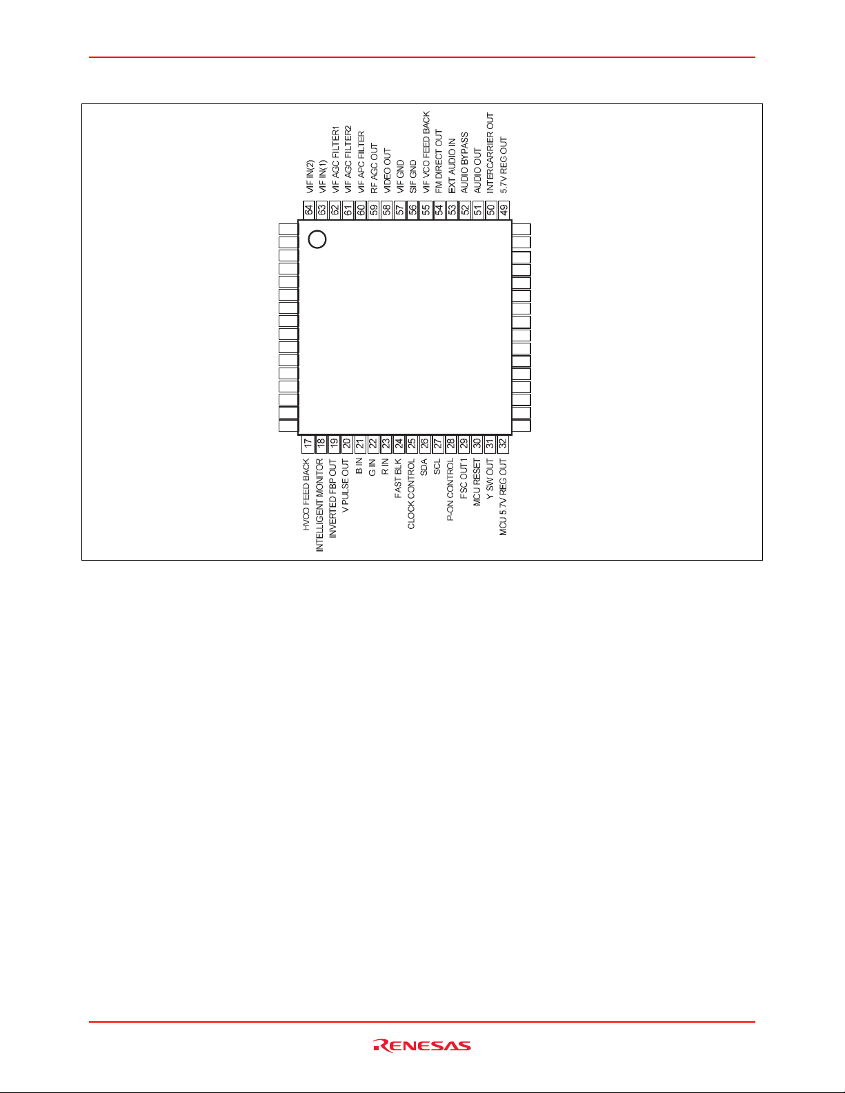
M61250BFP
R
Pin Configuration (Top View)
V RAM P CAP
AFT OUT
VIF V cc
SIF Vcc
RAMP OUT
V RAMP F/B
AFC FI LTER
DEF G ND
LOGIC GND
FBP IN
H OUT
DEF Vcc
R OUT
G OUT
B OUT
1
2
3
4
5
6
7
8
9
M61250BFP
10
11
12
NC
13
14
15
16
48
LIMITER IN
47
8.7V REG OUT
NC
46
45
NC
44
Hi Vcc
43
AUDI O AT T F I LT E R
42
VREG Vcc
41
TV/Y IN
40
VI DEO /CHRO MA Vc c
39
DRI VE Vc c
38
EXT/C I N
37
CHRO MA AP C F I LT E
36
VI DEO /CHRO MA G ND
DRI VE GN D
35
X-TAL 3.58
34
ACL/ABCL
33
Rev.1.0, Sep.23.2003, page 2 of 49
Page 3
M61250BFP
Pin Explanations
Pin No. Name Pin peripheral circuit DC voltage (V)
1 V RAMP CAP
2 AFT OUT 0.3 to 4.7
3
4
VIF V
SIF V
CC
CC
5.0 V
5 RAMP OUT 4.6
6 V RAMP FEED
BACK
Rev.1.0, Sep.23.2003, page 3 of 49
Page 4
M61250BFP
Pin Explanations (cont)
Pin No. Name Pin peripheral circuit DC voltage (V)
7 AFC FILTER 3.5 V
8
9
DEF GND
LOGIC GND
10 FBP IN VTH: 2.0 V
(FBP Vth L = OFF)
: 1.0 V
V
TH
(FBP Vth L = ON)
11 H OUT VOL: 0.0 V
: 5.4 V
V
OH
12 DEF V
CC
13 NC
14
15
16
R OUT
G OUT
B OUT
Rev.1.0, Sep.23.2003, page 4 of 49
Page 5
M61250BFP
Pin Explanations (cont)
Pin No. Name Pin peripheral circuit DC voltage (V)
17 H VCO
FEEDBACK
3.0 V
18
19 INV FBP OUT VOL: 0.0 V
20 V PULSE OUT VOL: 0.0 V
INTELLIGENT
MONITOR
: 5.0 V
V
OH
VOH: 5.0 V
Rev.1.0, Sep.23.2003, page 5 of 49
Page 6
M61250BFP
Pin Explanations (cont)
Pin No. Name Pin peripheral circuit DC voltage (V)
21
22
23
24 FAST BLK 0.0-0.5 V: INT RGB
B IN
G IN
R IN
(1) Digital OSD
VIL: 0.0 V
VIH: 3.0 V
(2) Analog OSD
0.7 Vp-p
1.5-3.0 V: H TONE
4.0-5.0 V: EXT RGB
25 CLK CONTROL VTH: 3.0 V
26 SDA VIL: 0.75 V
V
: 4.25 V
IH
Rev.1.0, Sep.23.2003, page 6 of 49
Page 7
M61250BFP
Pin Explanations (cont)
Pin No. Name Pin peripheral circuit DC voltage (V)
27 SCL VIL: 0.75 V
: 4.25 V
V
IH
28
29 fsc OUT 1 3.0 V
30 MCU RESET H: 5.0 V
POWER ON
CONTROL
VTH: 3.0 V
L: 0.0 V
Rev.1.0, Sep.23.2003, page 7 of 49
Page 8
M61250BFP
Pin Explanations (cont)
Pin No. Name Pin peripheral circuit DC voltage (V)
31 Y SW OUT 1.7 V
32 MCU 5.7 VREG
OUT
33 ACL/ABCL
34 X-TAL 3.58 3.3 V
5.7 V
35
36
Rev.1.0, Sep.23.2003, page 8 of 49
DRIVE GND
Video/Chroma
GND
0.0 V
Page 9
M61250BFP
Pin Explanations (cont)
Pin No. Name Pin peripheral circuit DC voltage (V)
37 CHROMA APC
FILTER
38 EXT/C IN 1.7 V
3.2 V
39
40
DRIVE V
CC
Video/Chroma
V
CC
5.0 V
41 TV/Y IN 1.7 V
42 VREG V
43
AUDIO ATT
CC
8.7 V
2.75 V to 3.25 V
FILTER
44 Hi V
45
CC
NC
46
Rev.1.0, Sep.23.2003, page 9 of 49
8 V
Page 10
M61250BFP
Pin Explanations (cont)
Pin No. Name Pin peripheral circuit DC voltage (V)
47 8.7 VREG OUT 8.7 V
48 LIMITER IN 2.5 V
49 5.7 VREG OUT 5.7 V
50
INTER
CARRIER OUT
2.3 V
Rev.1.0, Sep.23.2003, page 10 of 49
Page 11
M61250BFP
Pin Explanations (cont)
Pin No. Name Pin peripheral circuit DC voltage (V)
51 AUDIO OUT 2.3 V
52 AUDIO BYPASS 2.3 V
53 EXT AUDIO IN 3.0 V
54 FM DIRECT
OUT
3.0 V
Rev.1.0, Sep.23.2003, page 11 of 49
Page 12
M61250BFP
Pin Explanations (cont)
Pin No. Name Pin peripheral circuit DC voltage (V)
55 VIF VCO
FEEDBACK
3.0 V
56
57
58 VIDEO OUT 2.7 V
59 RF AGC OUT 0.3 to 4.7 V
SIF GND
VIF GND
60
Rev.1.0, Sep.23.2003, page 12 of 49
VIF APC
FILTER
3.0 V
Page 13
M61250BFP
Pin Explanations (cont)
Pin No. Name Pin peripheral circuit DC voltage (V)
61
62
VIF AGC
FILTER 2
VIF AGC
FILTER 1
2.3 V
63
64
VIF IN (1)
VIF IN (2)
1.6 V
Rev.1.0, Sep.23.2003, page 13 of 49
Page 14
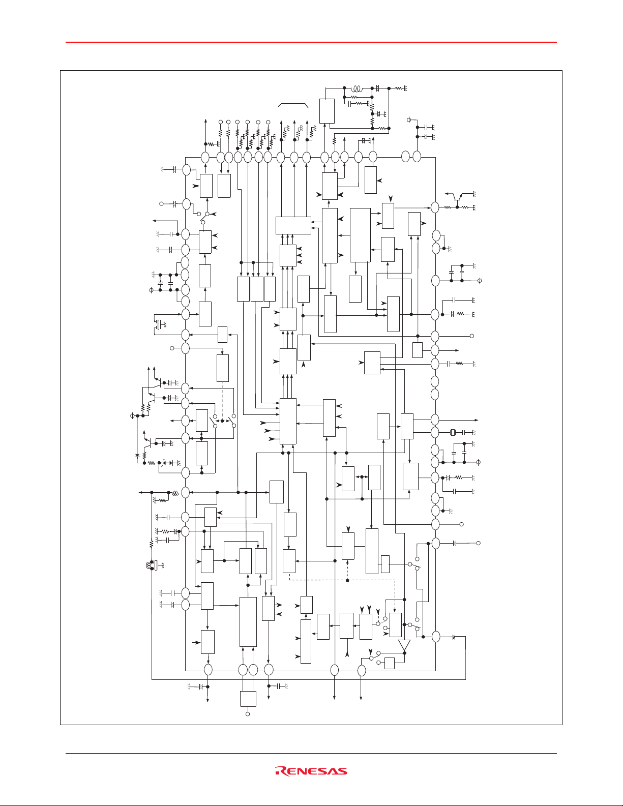
M61250BFP
C
Block Diagram
DY
OUT PUT
R
B
R IN
FAST BLK
G IN
SCL
AUDIO
OUT
SDA
G
B IN
VERTICAL
8V
V.OUT
V.PULSE
OUT
6
26
43
BUS
I / F
ATT
ATT
53
EXT AUDIO IN
DIRECT OUT
5V
cc 8V
Vcc 5V
V
11V
DD
5V
MCU V
VIDEO
OUT
1 Vp-p
54
52
56
57
3
4
LIMITER
IN
48
INTERCARRIEROUT
502849
from MCU
47
CU
30
ESET
R
to M
32
8.7V
4258556061
AUDIO SW
FM
AF
AMP
MUTE
VIF GND
FM
DET
R EXT
VIF Vcc
MITE R
LI
8.7V 5.7V
5.7V reg RESET
VCO
ADJ
VCO
VIF VCOADJ
INP UT
HPF
POWER ON
CONTROL
P-ON-ON
US/JPN
DET
VIDEO
14
15
HV
CLAMP
B EXT
INP UT
INP UT
G EX T
B
AMP
DRIVE
DRIVE
R
BRIGHT
BRIGHT
RGB
MATR IX
BLUE BACK
(WH ITE )
CONTRAST
APC
CONTRAST
COLOR
DET
LOCK
REF
FILTE R
ADJ
DET
DET
21
22
23
24
27
51
5
16
SERVICE SW
BLK
VERTICAL
B
G
R
CUT OFF
TRI G
V SYNC
SEP
SYNC
SYNC
SLICE
1
18
20
toring
Intelli gent
V.RAMP
COUNT DOWN
EQ
ELIMINATE
DEMODULATOR
KILLERB
Moni
V.SIZE
V.SHIFT
V COINB
BGP
HVCO ADJ
ANGLE
TIN T
DET
KILLER
TAKE OFF
BPF
CHROMA
Intelli gent Monitoring
AFC 2
H STOP
HORIZONTAL
COUNT DOWN
H VCO
GEN
AFC GAIN
VCO
ADJ
CLK CONT
DET
ACC
C
HPF
H-PHASE
DEF
Vcc
12
13
NC
H. OUTPUT
11
H
H COINB
COINCI.
DEF
GND
89
44
Hi Vcc
AFC 1
7
10
INV
17 19
NC NC
45 46
29
VCXO
3.58MHz
40 34
VIDEO/CHROMA
Vcc
37 39
DET
APC
CHROMA
36
35
VIDEO/CHROMA
GND
25
38
8V
FB P
IN
FB P
INV
OUT
fsc
OUT
5V
CLOCK
CONTROL
1Vp-p
EX T IN /C IN
IF AGC
62
VIF
AMP
LAY ADJ
RF AGC
DE
59
OUT
RF AGC
64
63
IN
VIF
SAW
IF IN
MUTE
A FT OUTDEFEAT
MUTE
AFT
2
AFT
OUT
VIDEO
VIDEO
CLAMP
GAMMA
GAMMA
BLACK STRETCH
BLACK
STRETCH
DL
TIME
DL
SW
FIN E
TRA P
TON E
VIDEO
DELAY
CHROMA
TRA P
x2
F.TR A P
Y SW
LPF
SHARPNESS
33
Y-SW OUT
ACL/ABCL
LPF
31
41
TV IN/ Y IN
1Vp-p
Rev.1.0, Sep.23.2003, page 14 of 49
Page 15

M61250BFP
0
Absolute Maximum Ratings
Item Symbol Rating Unit
Power supply voltage VCC 6.0, 10.0 V
Internal power dissipation Pd 2026 mW
Thermal derating Kt 16.2 mW/°C
Ambient operating temperature Topr −20 to +65 °C
Storage temperature Tstg −40 to +150 °C
Thermal Derating (Maximum Ratings)
2.5
2.0
1.5
1.38
1.0
(Ta = 25°C)
0.5
Internal Power dissipation Pd (W)
65
0 25 50 75 100 125 15
Ambient temperature (°C)
Rev.1.0, Sep.23.2003, page 15 of 49
Page 16

M61250BFP
I2C Bus Table
1. SLAVE ADDRESS= BAH(WRITE), BBH(READ)
A6 A5 A4 A3 A2 A1 A0 R/W
10111011/0
2. WRITE TABLE(input bytes )
SUB ADDRESS
HEX BIN D7 D6 D5 D4 D3 D2 D1 D0 INITIAL
00H 00000000
01H 00000001
02H 00000010 0 0 0 0000000H
03H 00000011 0 0 0 0000000H
04H 00000100 0 0 V1 V0 V0 V0 V0 V0 20H
05H 00000101 V0 V1 V0 V0 V0 V0 V0 V0 40H
06H 00000110 1 0 0 V0 V0 0 0 0 80H
07H 00000111 0 V1 V0 V0 V0 V0 V0 V0 40H
08H 00001000 V0 V1 V0 V0 V0 V0 V0 V0 40H
09H 00001001 0 0 0 0010004H
0AH 00001010 V1 V0 V0 V0 V0 V0 V0 V0 80H
0BH 00001011
0CH 00001100
0DH 00001101 1 0 0 0000080H
0EH 00001110 1 0 0 0000080H
0FH 00001111 1 0 0 0000080H
10H 00010000 0 0 1 0010024H
11H 00010001 0 0 1 0000020H
12H 00010010 0 0 0 0000000H
13H 00010011 0 0 0 0000000H
14H 00010100 0 0 0 0001103H
15H 00010101 0 0 0 0000000H
16H 00010110 1 0 0 1000090H
17H 00010111 0 V1 V0 V0 V0 V0 V0 V0 40H
18H 00011000
19H 00011001
1AH 00011010
1BH 00011011
1CH 00011100
DATA
(inhibited)
0
(inhibited)
0
Video Mute Audio EXT C. Clip level TRAP Off Video T Sharp ABCL
Audio Mute Audio ATT
ABCL Gain AFT Defeat Video Tone
EXTRGB C. Clip
VIF Defeat Tint Control
Blue Back Color Control
HV BLK OFF VOUT STOP FSC FREE HTONE SW
(inhibited)
0
(inhibited)
0
White Back V-free
(inhibited)
H-free V.1Window YSW LPF H Start Service SW V Shift
Black Strech Discharge Black Strech Charge
AFC1 Gain AFC2 Gain OSD level Analog OSD US/JPN SW Killer level
VSYNCDET
00000000
BGPFBP OFF Test2 (inhibited)
00000000
00000000
00000000
TEST4 VFREE INT VBLKSHIFT ON
00000100
100000040H
VIFFreq5875 VIF VCO ADJ
010000020H
VIF Video Out Gain Y/C EXT Y DL Fine Adj Y DL Time Adj
100000040H
100000040H
(inhibited)
Monitoring Gamma Control TRAP Fine Adj
Aoto slice down
Test1 (inhibited)
Test3 (inhibited)
FBP Vth L AFC2 H Phase
RF Delay Adj
Black Stre. Off
Contrast Control
(inhibited)
Brightness Control
Drive(R)
Drive(B)
Cut Off(R)
Cut Off(G)
Cut Off(B)
H VCO Adj
V-Size
S.Slice Down2 S.Slice Down1 (inhibited)
(reserved)
(inhibited)
VBLK SHIFT(inhibited)
NOTE: V0 / V1 ==> V- LATCH BIT
Take Off
00H
00H
00H
00H
04H
3. READ TABLE (output bytes)
SUB ADDRESS
00H 00000000 KILLERB (not asigned) VCOINB STDETB AFT0 AFT1 HCOINB (not asigned)
D7 D6 D5 D4 D3 D2 D1 D0
Rev.1.0, Sep.23.2003, page 16 of 49
Page 17

M61250BFP
Bus Functions
WRITE
FUNCTION BIT SUB
VIF
SIF
VIDEO
CHROMA
RF delay adj 7 00H D0-D6 RF AGC delay point adjustment 40H
VIF VCO adj 6 10H D0-D5 VIF VCC free-running frequency adjustment
VIF freq. 58.75 1 01H D6 IF 45.75/58.75 switching; 0: 45.75, 1: 58.75 MHz 0
VIF Video out
gain
AFT defeat 1 04H D6 AFT output on/off (defeat) switching; 0: AFT on (non defeat), 1: Defeat 0
VIF defeat 1 07H D7 VIF AGC gain normal/minimum switching; 0: AGC function,
Audio ATT 7 03H D0-D6 Pin 51 audio output level adjustment 00H
Audio EXT 1 02H D6 Audio internal signal and external signal input switching;
Audio mute 1 03H D7
Video tone 6 04H D0-D5 Sharpness level control 20H V Latch
Contrast control 7 05H D0-D6 Contrast level control 40H V Latch
EXTRGB
contrast clip
C. clip level 1 02H D5
Y DL time adj 2 06H D0-D1 Y signal delay adjustment X0H
Y DL fine adj 1 06H D2 Y signal delay fine adjustment 0
EXT 1 06H D3 Video input pins 41/38 switching; 0: pin 41, 1: pin 38 0 V Latch
Y/C 1 06H D4 Pins 38/41 composite input/YC input switching; 0: composite, 1: Y/C mode 0 V Latch
Y SW LPF 1 13H D5
Video tone
sharp
Video mute 1 02H D7 Y signal output on/off (mute) switching; 0: mute off, 1: mute 0
TRAP off 1 02H D4 Y signal chroma trap on/off switching; 0: trap on, 1: trap off 0
TRAP fine adj 2 12H D0-D1 Chroma trap frequency fine adjust X0H
Black stretch off 1 02H D1 Black stretch circuit on/off switching;
Black stretch
charge
Black stretch
discharge
Gamma control 2 12H D2-D3 Gamma level adjustment X0H
Tint control 7 07H D0-D6 Hue control 40H V Latch
Color control 7 08H D0-D6 Color level control 40H V Latch
Take off 1 02H D0 Chroma BPF take-off function on/off switching; 0: BPF; 1: take off 0
US/JPN SW 1 15H D1-D3 US mode/JPN mode switching; 100: US mode, 011: JPN mode 0
Killer level 1 15H D0
Fsc 1 09H D5 X ’tal oscillation circuit forced free-running mode; 0: off, 1: free-running 0
DATA DISCRIPTION INI-
ADD
(adjust by setting VIF Defeat = 1 to center the AFT output)
3 06H D5-D7 Pin 58 IVF video-detection-wave output level adjustment 80H
1: Defeat (minimum gain)
0: internal, 1: external
Pin 53 audio direct output on/off (mute) switching;
0: audio on (non-muted), 1: mute
1 05H D7 EXT RGB contrast lower-limit clipping on/off; 0: clipping on, 1: clipping off 0 V Latch
EXT RGB contrast lower-limit clipping level switching;
0: low (20H), 1: high (40H)
Pin 31 (Y SW OUT) output f-characteristic switching;
0: flat, 1: LPF (fc=700 kHz)
1 02H D3 Video tone level two level (sharp/soft) switching; 0: standard (soft), 1: sharp 0
0: black stretch on, 1: black stretch off
2 14H D4-D5 Black stretch charge time constant adjustment 0XH
2 14H D6-D7 Black stretch discharge time constant adjustment 0XH
Colorkiller sensitivity switching (active shallow direction);
0: 41 dB,1: 34 dB
NOTE
TIAL
20H
0
0
0
0
0
0
0
Rev.1.0, Sep.23.2003, page 17 of 49
Page 18

M61250BFP
Bus Functions (cont)
WRITE (cont)
FUNCTION BIT SUB
RGB
DEF
Brightness
control
Driver (R) 7 0BH D0-D6 R output level control 40H
Driver (B) 7 0CH D0-D6 B output level control 40H
Cut off (R) 8 0DH D0-D7 R output DC level control 80H
Cut off (B) 8 0EH D0-D7 G output DC level control 80H
Cut off (B) 8 0FH D0-D7 B output DC level control 80H
Blue back 1 08H D7 Blue back screen on/off switching; 0: off, 1: blue back 0
White back 1 10H D7 White raster on/off switching; 0: off, 1: white back 0
ABCL 1 02H D2 ABCL on/off switching; 0: off, 1: ABCL on 0
ABCL gain 1 04H D7 ABCL sensitivity low/high switching; 0: low, 1: hi 0
OSD level 1 15H D5 OSD level (70%/90%) switching; 0: 70%, 1: 90% 0
HTONE SW 1 09H D4 Halftone on/off switching; 0: off, 1: halftone 0
Analog OSD 1 15H D4 OSD input digital/analog switching; 0: digital, 1: analog 0
AFC2 H phase 5 16H D0-D4 Screen horizontal position adjustment 90H
Ramp stop 1 09H D6
Service SW 1 13H D3 Vertical output on/off switching; 0: vertical output on, 1: vertical output off 0
H start 1 13H D4 Horizontal output out/stop switching; 0: stop, 1: H out 0
AFC 1 gain 1 15H D7 Horizontal AFC gain a high/low switching; 0: low, 1: hi 0
AFC 2 gain 1 15H D6 Horizontal AFC2 gain high/low switching; 0: high, 1: low 0
H VCO adj 3 10H D0-D2 H VCO free-running frequency adjustment 24H
V shift 3 13H D0-D2 Vertical ramp start timing adjustment X0H
V-size 6 11H D0-D5 Vertical ramp amplitude adjustment 20H
H-free 1 13H D7
V-free 1 10H D6 Vertical output forced free-running mode on/off switching;
S slice down 1 1 14H D2 Sync detection slice level (50%/30%) switching; 0: 50%, 1: 30% 0
S slice down 2 1 14H D3 Sync detection slice level (50%/40%) switching; 0: 50%, 1: 40% 0
Audio slice
down
FBP Vth L 1 16H D5 Pin 10 (FBP in) slice level switching during image period;
HV BLK OFF 1 09H D7 Horizontal/vertical blanking on/off switching; 0: blanking on, 1: blanking off 0
V SYNK DET 1 16H D7 Vertical minimum sync detection width switching;
1 window 1 13H D6 Vertical sync detection switching (1 window/2 window s);
BGPFBP OFF 1 19H D7 Internal BGP on/off switching when no FBP input; 0: BGP on, 1: BGP off 0
VREF INT 1 1CH D6 Interface/non-interface switching at vertical free-running 04H
VBLK SHIFT
ON
VBLK SHIFT 3 1CH D0-D2 D0-D2: VBLK SHIFT (Initial value: 100=4) 04H
Monitoring 4 12H D4-D7 Pin 18 intelligent monitoring mode switching 0XH
Test1 1 18H D6-D7 NO use for Customer (Test bit) 0
Test2 1 19H D6 NO use for Customer (Test bit) 0
Test3 1 1AH D6-D7 NO use for Customer (Test bit) 0
Test4 1 1CH D6 NO use for Customer (Test bit) 04H
DATA DISCRIPTION INI-
ADD
8 0AH D0-D7 Bright level control 80H V Latch
Pin 5 VOUT (ramp/pulse) forced stop mode (when stopped, pin 5 at DC
GND level); 0: VOUT, 1: STOP
Horizontal output forced free-running mode on/off switching;
0: off, 1: horizontal free-running
0: off, 1: vertical free-running
1 16H D6
1 1CH D3 0: Normal (VBLK shifts by VSHIFT),
Sync detection slice level (50%/40%) switching during image period;
0: slice level fixed, 1: slice level reduced
0: Vth = 2V (HBLK width: narrow), 1: Vth = 1 V (HBLK width: wide)
0: sync detect width =18 µs, 1: sync detect width =14 µs
0: 2 windows, 1: 1 window
1: Vertical blanking width can be setted by un-interlocking VSHIFT
NOTE
TIAL
0
0
0
0
0
90H
0
04H
Rev.1.0, Sep.23.2003, page 18 of 49
Page 19

M61250BFP
READ
FUNCTION BIT SUB
KILLERB 1 00H D7 Colorkiller information output; "1" when killer off
AFT0 1 00H D3 AFT information output (See note 1)
AFT1 1 00H D2 AFT information output (See note 1)
HCOINB 1 00H D1 Horizontal sync detection; "1" when asynchronous
FM STDETB 1 00H D6 FM radio mode detection; "1" when not detected
VCOINB 1 00H D5 Vertical sync detection; "1" when asynchronous
STDETB 1 00H D4 TF mode detection; "1" when not detected
Note: 1. <READ BYTE: AFT OUTPUT>
DATA DISCRIPTION
ADD
Rev.1.0, Sep.23.2003, page 19 of 49
Page 20

M61250BFP
Test Circuits
SCL
FAS TB LK
SDA
IN
EXT R IN
EXT G IN
EXT B IN
A
A
SIF IN
N.K.D
Part
number
M351T01
120p
0.01µ
0.01µ
8.2K
50
75
75
47µ
3.579545MHz
47µ
+
+
4.7µ
0.015µ
1µ
1µ
1µ
0.01µ
A
P30
P31
P32
P29
P24
P20
P19
P18
P17
17181920212223242526272829303132
P33
33
34
35
36
P37
37
38
39
40
41
42
1µ
43
+
M61250BFP
44
45
46
47
P47
48
P16
16
15
14
13
12
11
10
9
8
7
6
5
2.2K
P15
2.2K
P14
2.2K
0.01µ
A
20K
0.01µ
SW7
6.8K
47µ
10K
0.01µ
1µ
P11
P10
P7
P6
P5
4
3
2
1
47µ
0.1µ
P2
P1
1µ
64636261605958575655545352515049
P50P49
P53P52 P54 P55 P58 P59 P60
P51 P61
P62
50
Rev.1.0, Sep.23.2003, page 20 of 49
VR 20K
1162153144135126117108
M74LS221P
9
4700p
Page 21

M61250BFP
Input Signals
1. 10.1 VIF/SIF Block
SG No. Signal description (50 Ω termination)
SG1 fo = 45.75 MHz, 90 dBµ, fm = 20 kHz, AM 77.8%
SG2 fo = 58.75 MHz, 90 dBµ, fm = 20 kHz, AM 77.8%
SG3 fo = 45.75 MHz, 90 dBµ, CW
SG4
SG5 fo = 45.75 MHz, amplitude width variable, fm = 20 kHz, AM 77.8%
SG6 fo = 45.75 MHz, amplitude width variable, fm = 20 kHz, AM 16%
SG7 fo = 45.75 MHz, 80 dBµ, fm = 20 kHz, CW
SG8 fo = 45.75 MHz, 110 dBµ, fm = 20 kHz, CW
SG9 fo = 40.75 to 50.75 MHz (frequency variable), 90 dBµ, CW
SG10 fo = 45.75 MHz, 90 dBµ, CW
SG11 fo = 45.75 MHz, 90 dBµ, CW
SG12 fo = 53.75 to 63.75 MHz (frequency variable), 90 dBµ, CW
SG13
SG14
SG15 fo = 45.75 MHz, 93 dBµ, CW
SG16 fo = 45.75 MHz, 73 dBµ, CW
SG17 fo = 4.5 MHz, 100 dBµ, fm = 400 Hz, FM ±25 kHz dev.
SG18 fo = 4.5 MHz, 100 dBµ, fm = 400 kHz, AM 30%
SG19 fo = 4.5 MHz, 100 dBµ, CW
SG20 fo = 400 Hz, 500 mVrms, CW
SG21 fo = 0.5 to 8.5 MHz, 100 dBµ, fm = 400 kHz, FM ±25 kHz dev.
f1 = 45.75 MHz, 90 dBµ, CW
f2 = 45.75 ± 4.5MHz, 70 dBµ, CW
f1 = 45.75 MHz, 90 dBµ, RED raster signal, AM = 87.5% video modulation,
f2 = 4.5 ± 4.5MHz, CW, P/S = 20 dB
fo = 45.75 MHz, standard 10-step wave, sync rate: 28.6%, AM = 87.5% video modulation,
sync chip level: 90 dBµ
Rev.1.0, Sep.23.2003, page 21 of 49
Page 22

M61250BFP
s
s
2. Video/Chroma/RGB/DEF Bloc k
SG No. Signal description (75Ω termination)
NTSC format APL 100% typical
video signal. Vertical signal is
interlaced at 60 Hz.
SG. A
4.7µs
1.5µs 5.8µs
1V
0.714V
p-p
0.286V
SG. B
SG. C
SG. D
SG. E
In the SG.A signal, the Lumi. signal
frequency and amplitude can be
changed. However, typical amplitude
is 0.714 Vp-p.
In the figure on the right, the Lumi.
signal is represented by f.
NTSC typical monochrome video
signal. Vertical signal is interlaced
at 60 Hz.
0.286V
NTSC format video signal;
APL variable. Vertical signal is
interlaced at 60 Hz.
NTSC format monochrome video signal.
In the SG.C signal, the burst and chroma
part frequency and amplitude can be changed.
Vertical signal is interlaced at 60 Hz.
V
Typical state:
Veb=0.286V,
Vec=0.572V
f eb=f ec=3.579545MHz
eb
4.7µs
1.5µs 5.8µs
4.7µs
0.286V
4.7µs
1.5µs 5.8µs
4.7µs
0.286V
f
ebfec
1.5µs5.8µs
V
y
0.286V
1.5µs5.8µs
f
0.572V
V
ec
Fast blanking signal; synchronized with
video input signal.
0V
20µs 24µ
SG. F
Rev.1.0, Sep.23.2003, page 22 of 49
Fast blanking signal;
synchronized with video input signal.
0V
20µs 24µ
2.0V
V
osd
Page 23

M61250BFP
2. Video/Chroma/RGB/DEF Block (cont)
SG No.
SG. G
SG. H
SG. I
SG. J
Signal description (75Ω termination)
NTSC format rainbow color bar video signal.
Vertical signal is interlaced at 60 Hz.
Duty 90%, variable frequency, variable level. (Typical: 1 Vp-p)
1V
Duty variable (typical 95%), frequency variable, level variable
(Typical: 1 Vp-p)
1V
NTSC format typical color bar
video signal;
4.7µs
0.714V
vertical signal is interlaced at 60 Hz.
p-p
p-p
SG. K
0.286V
1.5µs 5.8µs
NTSC format, typical 8-step wave signal;
vertical signal is interlaced at 60 Hz.
Rev.1.0, Sep.23.2003, page 23 of 49
Page 24

M61250BFP
(
)
Setup instruction for evaluation PCB
1. Horizontal blanking pulse adjustment
The horizontal blanking pulse timing and pulse width are adjusted using the variable resistances of a one-shot
multivibrator, as shown below.
Pin 11 (H OUT)
8µs
Horizontal
blanking pulse
12µs
The timing is adjusted to 8 µs using the pin 15 variable resistance of the M74LS221P TTL IC. Also, the pulse width is
adjusted to 12 µs using the pin 7 variable resistance.
2. VIF VOC adjustment
Before carrying out the M61250BFP measurements, the VIF VCO should be adjusted using the following procedure.
(1) Input the I
(2) Input the I
(3) Adjust the I
2.5 V.
(4) Input the I
2
C bus data for the VIF frequency (01H D6) based on the IF frequency. (45.75 MHz: 0, 58.75 MHz: 1)
2
C bus data for VIF Defeat ON (07H D7 = 1).
2
C bus data for the VCO control (01H D0 – D5) so that the voltage of Pin 2 (AFT OUT) is closest to
2
C bus data for VIF Defeat OFF (07H D7 = 0).
Voltage
2.5V
45.75MHz
Frequency
or 58.75MHz
3. H VCO adjustment
Prior to measurement of the M61250BFP, the following method is used for H VCO adjustment.
(1) The H VCO control I
15.734 kHz.
Rev.1.0, Sep.23.2003, page 24 of 49
2
C bus data (1 CH D0-D3) is adjusted, and the pin 11 (H OUT) frequency is set to approx.
Page 25

M61250BFP
Electrical Characteristics
Subaddress
(Ta = 25°C)
Unit Notes
Limits
Test
point
Input signal
00H 01H 02H 03H 04H 05H 06H 07H 08H 09H 0AH 0BH 0CH 0DH 0EH 0FH 10H 11H 12H 13H 14H 15H 16H 17H 18H 19H 1AH 1BH 1CH
Pin 28=5 V, pin 25=5 V, pin 24=0 V 40 20 02 00 20 40 80 40 40 00 80 40 40 80 80 80 24 20 00 10 00 00 88 40 00 00 00 00 00
95 115 135 mA VIF/SIF/VIDEO/Chroma Vcc
Min. Typ. Max
0
3,4,39,4
SG
--
Pin
Reference data
Reference data
VIF/SIF/Vcc
VIDEO/Chroma Vcc
-57-mA
39,40
- - 3,4 - 57 - mA
--
Reference data
Reference data
Deflection Vcc
RGB Drive 8V Vcc
Pin 28=5 V, pin 25=0 V, pin 24=0 V 40 adj 02 00 20 40 80 40 40 00 80 40 40 80 80 80 24 20 00 10 00 00 88 40 00 00 00 00 00
32 42 52 mA Deflection/RGB Drive 8V Vcc
12,44
--
- - 42 4 6 8 mA 8.7 VREG Vcc
- - 12 - 25 - mA
- - 44 - 17 - mA
40 adj 02 00 20 40 80 40 40 00 80 40 40 80 80 80 24 20 00 10 00 00 88 40 00 00 00 00 00
Pin 28=5 V
Pin 28=0 V
Pin 28=5 V
- - 28 2.6 3 3.4 V
- - 32 5.4 5.65 5.9 V
- - 32 5.4 5.65 5.9 V Pin 28=0 V
Pin 28=5V, pin 25=5V
- - 30 - 0 0.5 V
- - 32 4 4.2 4.4 V
- - 30 4.5 5 5.5 V
Reference data
Pins 3 and 4 current
Pins 39 and 40 current
Pin 12 current drawn
Pin 44 current drawn
8V current drawn by the
circuit
ICC8V
by the circuit
by the circuit
ICC44
ICC12
Pin 42 current drawn
by the circuit
ICC42
Power supply circuit
typical conditions
Power
Symbol Item
5V current drawn by the
circuit (pins 3, 4, 39, 40)
Typical conditions
drawn by the circuit
ICC
ICC5V
ICC34
drawn by the circuit
ICC3940
Rev.1.0, Sep.23.2003, page 25 of 49
Power on control
threshold voltage
Vth28
V47H 8.7 VREG output voltage 1 - 47 8.3 8.7 9.1 V Pin 28=5 V
V47L 8.7 VREG output voltage 2 - 47 - 0 0.3 V
MCU 5.7 VREG
output voltage 1
V49 5.7 VREG output voltage 1 - 49 5.5 5.75 6.0 V
V32H1
MCU 5.7 VREG
output voltage 2
Reset typical conditions
Maximum reset output
V32H2
Reset
V30H
Minimum reset output
voltage
Reset threshold voltage
voltage
TH32
V30L
IIC IIC typical conditions ------- 40adj020020408040400080404080808024200010000088400000000000
ACK current - - - 1 - mA
ACK
I
Clock frequency - - 27 - - 100 kHz
SCL
VIL SCL/SDA VTH(L) - - 26,27 0.0 0.75 1.5 V
VIH SCL/SDA VTH(H) - - 26,27 3.5 4.25 5.0 V
F
Page 26

M61250BFP
Subaddress
80
Unit Notes
Limits
Test
point
Input signal
00H 01H 02H 03H 04H 05H 06H 07H 08H 09H 0AH 0BH 0CH 0DH 0EH 0FH 10H 11H 12H 13H 14H 15H 16H 17H 18H 19H 1AH 1BH 1CH
Min. Typ. Max.
SG
Pin
- - 58 2.2 2.7 3.2 V Pin 62=0 V
63,64 SG1 58 0.8 1.2 1.5 Vpp
+40
63,64 SG2 58 0.8 1.2 1.5 Vpp
63,64 SG4 58 4 5.4 - MHz
+40
+40
Reference data
pp
mV/kHz
SG13 58 - 42 - dB
63,64 SG5 58 - 45 50 dBµ
63,64 SG6 58 100 108 - dBµ
63,64 SG9 2 7 10 13
- - 58 2.6 4.0 - MHz VCU45-VCL45
63,64 SG9 58 1.5 2.2 - MHz Center frequency=45.75MHz
63,64 SG9 58 - -1.8 -1.1 MHz Center frequency=45.75MHz
- - 58 2.6 4.0 - MHz VCU58-VCL58
63,64 SG12 58 1.5 2.2 - MHz Center frequency=58.75MHz
63,64
63,64 SG12 58 - -1.8 -1.1 MHz Center frequency=58.75MHz
Input sensitivity
Maximum allowable input
Video frequency
characteristics
output (48.75 MHz)
Vf
Vo5875
P/N Video S/N 63,64 SG3 58 43 50 - dB
Vin min
Vin max
GR AG control range - - - 50 - - dB Vo max - Vo min
Symbol Item
Video-detection-waveform
output (45.75 MHz)
Video-detection-waveform
Video-detection-waveform
output direct current voltage
VIF IF typical conditions Pin 28=5 V, pin 25=5 V, pin 24=0 V 40 adj 02 00 20 40 80 40 40 00 80 40 40 80 80 80 24 20 00 10 00 00 88 40 00 00 00 00 00
Vdc
Vo4575
Rev.1.0, Sep.23.2003, page 26 of 49
AFT-detection-waveform
sensitivity
V63H IF AGC maximum voltage - - 62 3.8 4.3 4.8 V
Vdefeat VIF DETEAT function 63,64 SG1 58 0 0.1 0.2 V
V63T IF AGC voltage (80 dBµ) 63,64 SG7 62 2.3 2.8 3.3 V
V63L IF AGC minimum voltage 63,64 SG8 62 1.3 1.8 2.3 V
µAFT
V60H AFT maximum voltage 63,64 SG10 2 4.2 4.7 - V
V60L AFT minimum voltage 63,64 SG11 2 - 0.3 0.8 V
Capture range
V60D AFT DETEAT function - - 2 2.0 2.5 3.0 V 80
VCU45
(45.75MHz upper)
Capture range
(45.75MHz lower)
Capture range
(45.75MHz total)
VCT45
VCL45
Capture range
(58.75MHz upper)
Capture range
(58.75MHz lower)
Capture range
VCU58
VCL58
(58.75MHz total)
Inter modulation
IM
VCT58
Page 27

M61250BFP
Subaddress
20 40 80 40 40 00 80 40 40 80 80 80 24 20 00 10 00 00 88 40 00 00 00 00 00
80
7F
Unit Notes
Limits
Test
point
Input signal
00H 01H 02H 03H 04H 05H 06H 07H 08H 09H 0AH 0BH 0CH 0DH 0EH 0FH 10H 11H 12H 13H 14H 15H 16H 17H 18H 19H 1AH 1BH 1CH
Reference data
Min. Typ. Max.
SG
SG14 58 - 3 - %
Pin
63,64
Reference data
SG14 58 - 3 - deg
63,64
40 adj 02 00
7F
00-
Variable input frequency
Pin 28=5 V, pin 25=5 V, pin 24=0 V
rms
- - - 33 43 - dBµ DLPH-DLPL
63,64 SG5 59 - 58 71 dBµ 7F
63,64 SG5 59 95 108 - dBµ 00
48 SG17 54 - 46 58 dBµ
Variable input frequency
rms
48 SG17 51 280 400 550 mV
48 SG21 54 5.5 7.5 - MHz
48 SG21 54 - 3 4.0 MHz
48 SG17 51 - -80 -69 dB
RF AG delay point
adjustment range
RF AG delay minimum
point
RF AG delay maximum
point
Symbol Item
DG DG
DP DP
V62H RF AG maximum voltage 63,64 SG15 59 4.3 4.8 - V
DLPL
DLP
SPN Sync rate 63,64 SG14 58 25 28 33 %
V62L RF AG minimum voltage 63,64 SG16 59 - 0.2 0.7 V
DLPH
SIF SIF typical conditions
Rev.1.0, Sep.23.2003, page 27 of 49
SIF capture range
(upper)
SIF capture range
GEAu EXT Audio gain 53 SG20 51 -4.1 -2.1 -0.1 dB 40 7F7FSCFU
(lower)
Audio output maximum
amplitude
Audio output maximum
attenuation
SCFL
VOL-
max
VOL-min
Input limit sensitivity
VAF AF direct output DC voltage - - 54 2.2 3.0 3.8 V
VoAF AF direct output voltage 48 SG17 54 280 400 520 mV
THD AF AF distortion rate output 48 SG17 54 - 0.5 3 %
LIM
AM AMRR 48 SG18 54 48 54 - dB
AFSN AF S/N 48 SG19 51 49 55 - dB
Page 28

M61250BFP
Subaddress
03
00-
00
00
8C
7F 8C
Unit Notes
Limits
Test
point
Input signal
00H 01H 02H 03H 04H 05H 06H 07H 08H 09H 0AH 0BH 0CH 0DH 0EH 0FH 10H 11H 12H 13H 14H 15H 16H 17H 18H 19H 1AH 1BH 1CH
Min. Typ. Max.
SG
Pin
pp
pp
- - -18 dB 8C 00 02
2.9 4.2 5.6 V 7F 8C 00
16
16
16
14,15,
14,15,
14,15,
-------Pin 28=5 V, pin 25=5 V, pin 24=0 V 40 adj 02 00 20 40 80 40 40 00 80 40 40 80 80 80 24 20 00 10 00 00 88 40 00 00 00 00 00
41 SG.A 31 1.6 2.0 2.6 V
38 SG.A 31 1.6 2.0 2.6 V
38 SG.A
38 SG.A
38 SG.B
16
14,15,
38 SG.C
14,15,
SG.C
38
190 260 330 nS 8C 00
120 200 280 nS YDL2=measured value -YDL1 measured value 8D 00
120 200 280 nS YDL3=measured value -YDL2 measured value 8E 00
16
16
16
38
14,15,
14,15,
383838
16
14,15,
- - -20 dB At Trap fine adj. adjustment 8C 00
-4 -1 - dB f=5MHz, C-trap : OFF 10
12 15 18 dB 7F 8C
120 200 280 nS YDL4=measured value -YDL3 measured value 8F 00
16
14,15,
A
1.0 1.4 1.8 V f=2.5MHz 8C 00
14,15,
B
SG.
38
7 10 14 dB f=2.5MHz 3F 8C 00
-6 -2 2 dB f=2.5MHz 00 8C 00
-1 2 5 dB f=2MHz 8C 00
16
16
16
B
SG.
38
14,15,
B
SG.
38
16
14,15,
B
SG.38SG.
38
14,15,
-9 -5 -1 dB f=5MHz 8C 00
14,15,
B
- -45 -35 dB 80 7F 8C 00
0.01 0.03 0.05 V adj 8C 00 adj 80
16
16
16
14,15,
14,15,
38 SG.K
38 SG.A
Chroma trap maximum
attenuation
Chroma trap attenuation 1
characteristic
TRF
FBY
CRF1
YDL1 YDL time 1 SG.A
Symbol Item
Video typical conditions
Video SW output level
(TV input)
Video SW output level
(External input)
Maximum video output
VIDEO
2AGTV
2AGEV
Ymax
Video frequency
Video gain
GY
Rev.1.0, Sep.23.2003, page 28 of 49
Video tone control
characteristic 1
Video tone control
characteristic 2
Video tone control
characteristic 3
Video tone control
characteristic 4
Video tone control
characteristic 5
Black expansion
characteristic
Video mute function
YDL2 YDL time 2 SG.A
YDL3 YDL time 3 SG.A
YDL4 YDL time 4 SG.
GTnor
GTmax
GTmin
GT2M
GT5M
BLS
VMF
Page 29

M61250BFP
Subaddress
00H 01H 02H 03H 04H 05H 06H 07H 08H 09H 0AH 0BH 0CH 0DH 0EH 0FH 10H 11H 12H 13H 14H 15H 16H 17H 18H 19H 1AH 1BH 1CH
40
40
40
80 40
80
80
80 40
C0/
80
C0/
C0/
40
40
80
C0/
40
40
80
80
80
C0/
C0/
C0/
02
FF 06
88
88
88
20 88 FF 08
20 88 FF 08
88
88
88
20 88 FF 06
20 88
88
88
88 20
40 adj 02 00 20 40 80 40 40 00 80 40 40 80 80 80 24 20 00 10 00 00 88 40 00 00 00 00 00
Unit Notes
Limits
Min. Typ. Max.
Test
point
SG
-------Pin 28=5 V, pin 25=5 V, pin 24=0 V
Input signal
Pin
Chroma typical output
Chroma typical c
onditions
Symbol Item
CHROM
A
Veb, Vec: typical input level +6 dB
E59 -3 0 3 dB 88 80 40
SG.C 59 640 920 1290 mV 88 80 40
38
38 SG.C 59 390 560 790 mV 88 C0 40
(R-Y)
CnorR
38
38
Chroma typical output
(B-Y)
CnorB
ACC1 ACC characteristic 1 SG.
ACC2 ACC characteristic 2 SG.E 59 -4.5 0 1.5 dB Veb, Vec: typical input level -20 dB 88 80 40
= 0mV 80 40
eb
38 SG.E 59 - -43 -35 dB Veb, Vec: variable 88
38 SG.E 59 -3 2 5 dB V = 800 mV 80 40
38 SG.E 59 - -45 -30 dB V
Killer operation input
level
Chroma overload
characteristic
Color remaining on
VikN
OV
KillP
colorkilling
APCU APC pull-in range (upper) 38 SG.E 59 - -600 -300 Hz feb=fec: variable 88 80 40
+50kHz
eb
=f
ec
38 SG.E 59 0.40 0.57 0.80 - f
Demodulation ratio
APCL APC pull-in range (lower) 38 SG.E 59 300 600 - Hz feb=fec: variable 88
R/BN
Reference data
Reference data
Reference data
- 1.33 - -
- 0.43 - -
- 1.31 - -
14,15
15,16
14,15
38 SG.J
38 SG.J
38 SG.J
Demodulation ratio
Demodulation ratio
Demodulation ratio
(US mode)
(US mode)
(JPN mode)
R/BU
G/BU
R/BJ
+50kHz
+50kHz
eb
eb
=f
=f
ec
ec
Reference data
- 0.47 - -
15,16
E 59 73 90 107 deg f
SG.38SG.38SG.
38
38 SG.J
Demodulation ratio
Demodulation angle 2
(JPN mode)
R-YN2
G/BJ
R-YN1 Demodulation angle 1 E 59 86 103 120 deg f
+50kHz F7 80 40
+50kHz 00 80 40
ec
ec
=f
=f
eb
eb
E59304560degf
E59304560degf
SG.
38
TINT control
characteristic 1
TINT control
characteristic 2
TC1
TC2
MHz 88
3.5793 3.5796 3.5799
29
Ffsc fsc output frequency 38 SG.C
pp
SG.
38
Vfsc fsc output amplitude 1 C 29 1.4 2 2.6 V
pp
MHz 88 20
3.5790 3.5795 3.5810
29
38 SG.C 29 1.4 2 2.6 V
38 SG.C
fsc output amplitude 1
in fsc free mode
fsc output frequency
in fsc free mode
Vfsc
Ffscfree
Rev.1.0, Sep.23.2003, page 29 of 49
Page 30

M61250BFP
Subaddress
00 00
Unit Notes
Limits
Test
point
Input signal
00H 01H 02H 03H 04H 05H 06H 07H 08H 09H 0AH 0BH 0CH 0DH 0EH 0FH 10H 11H 12H 13H 14H 15H 16H 17H 18H 19H 1AH 1BH 1CH
Min. Typ. Max.
SG
Pin
0 0.1 0.3 V 88 00
14,15,
SG.A
38
00
f=100kHz 88
pp
2.2 2.8 3.3 V
16
14,15,
SG.B
00
88
00
- 200 300 mV f=100kHz
16
16
14,15,
14,15,
SG.B
383838
88 00
00 88 00
= 0.0V 88 00
= 0.0V 88 00 FF
= 0.0V 88 00 00
y
y
1.7 2.1 2.5 V V
14,15,
D
y
- 1.3 2 V V
2.3 3 - V V
16
16
16
14,15,
14,15,
D
A 16 2.0 4.0 6.0 dB 88 00 00 7F
D
Pin 33 =0.0 V
Pin 24 =2.5 V
- 100 200 mV
2.2 2.8 3.3 V Pin 33 =2.9 V 88 00
0.50 0.65 0.80 V
16
16
16
14,15,
14,15,
A
SG.F
SG.A
SG.38SG.38SG.38SG.38SG.38SG.38SG.38SG.
38
23
21,22,
000000
888888
= 1.0V, SW23=ON
osd
V
pp
14 1.0 1.5 2.0 V
SG.A
SG.F,
38
23,24,
00
88 00 20
= 1.0V, SW22=ON
= 1.0V, SW21=ON
osd
osd
Vosd = 1.0V, SW23=ON
EXD2(R)=Measured value - EXD1(R)
V
V
pp
pp
15 1.0 1.5 2.0 V
16 1.0 1.5 2.0 V
14 200 300 400 mV
SG.A
SG.A
SG.F,
22,24,
SG.A
SG.F,
SG.F,
38
38
38
21,24,
23,24,
88 00 20
88 00 20
Vosd = 1.0V, SW22=ON
EXD2(G)=Measured value - EXD1(G)
Vosd = 1.0V, SW21=ON
EXD2(B)=Measured value - EXD1(B)
15 200 300 400 mV
16 200 300 400 mV
SG.A
SG.A
SG.F,
SG.F,
- - - -350 0 350 mV 88
21,24,
- - - -350 0 350 mV 88
38
22,24,
38
= 0.7V 40 88 00 10
= 0.7V 40 88 00 10
= 0.7V 40 88 00 10
osd
osd
osd
V
V
V
pp
pp
pp
14 1.2 2.1 3.0 V
15 1.2 2.1 3.0 V
16 1.2 2.1 3.0 V
SG.A
SG.A
SG.F,
- - - -350 0 350 mV 88
23,24,
SG.A
SG.F,
SG.F,
38
38
38
22,24,
21,24,
Symbol Item
RGB typical conditions -------Pin 28=5 V, pin 25=5 V, pin 24=0 V 40 adj 02 00 20 40 80 40 40 00 80 40 40 80 80 80 24 20 00 10 00 00 88 40 00 00 00 00 00
Output blanking voltage
Contrast control
characteristic 1
RGB
VBLK
GYtyp
Contrast control
characteristic 2
Contrast control
characteristic 3
Contrast control
GYmin
GYEnor
characteristic 4
GYEmin
Brightness control
Contrast control
characteristic 5
Brightness control
characteristic 1
GYEclip
Lum nor
characteristic 2
Lum max
Rev.1.0, Sep.23.2003, page 30 of 49
R driving control
characteristic 1
B driving control
characteristic 3
Lum min
D(R)1 A 14 2.0 4.0 6.0 dB 88 00 00 7F
characteristic 1
D(B)1
Brightness control
R driving control
characteristic 2
B driving control
characteristic 3
Digital OSD (R)
D(R)2 A 14 -5.0 -3.0 -1.0 dB 88 00 00 00
D(B)2 A 16 -5.0 -3.0 -1.0 dB 88
EXD1(R)
I/O characteristic 1
Digital OSD (G)
I/O characteristic 1
Digital OSD (B)
I/O characteristic 1
EXD1(G)
EXD1(B)
Digital OSD (R)
I/O characteristic 2
Digital OSD (G)
I/O characteristic 2
Digital OSD (B)
EXD2(R)
EXD2(G)
EXD2(B)
I/O characteristic 2
Digital OSD (R-G)
amplitude difference
Digital OSD (G-B)
amplitude difference
Digital OSD (B-R)
EXD1(R-
G)
EXD1(G-
B)
EXD1(B-
Analog OSD (R)
I/O characteristic
amplitude difference
Analog OSD (G)
I/O characteristic
Analog OSD (B)
EXA(R)
EXA(G)
R)
I/O characteristic
EXA(B)
Page 31

M61250BFP
Subaddress
10
7F 88
7F 88
Unit Notes
Limits
Test
point
Input signal
00H 01H 02H 03H 04H 05H 06H 07H 08H 09H 0AH 0BH 0CH 0DH 0EH 0FH 10H 11H 12H 13H 14H 15H 16H 17H 18H 19H 1AH 1BH 1CH
Min. Typ. Max.
SG
Pin
= 1.0V 7F 88 10
= 1.0V 7F 88
= 1.0V, SW23=ON
osd
osd
osd
14 - 0.05 0.13 us V
14 - 0.05 0.13 us V
14 - 0.05 0.13 us V
SG.A
SG.A
SG.F,
SG.F,
SG.F,
38
38
23,24,
23,24,
23,24,
SG.A
38
14 1.7 2.1 2.5 V 88 80
SG.A
38
15 1.7 2.1 2.5 V 88 80
SG.A
38
2.7 3.7 4.7 V 88 A0
16
14,15,
SG.A
38
38 SG.A 16 2.7 3.7 4.7 V 88 80
15,16 0.29 0.37 0.45 - 88
14,16 0.81 0.98 1.08 - 88
SG.G38SG.G
38
= 1.0V, SW23=ON
osd
14 - 0.05 0.13 us V
SG.A
SG.F,
38
23,24,
= 0.0V 88 00
= 0.0V 88 00
= 0.0V 88 00 FF
= 0.0V 88 00 FF
= 0.0V 88 00 FF
= 0.0V 88 00 00
= 0.0V 88 00 00
y
y
y
y
y
D 16 2.6 2.9 3.2 V V
SG.
_ _ _ -350 0 350 mV 88 10
_ _ _ -350 0 350 mV 88 10
_ _ _ -350 0 350 mV 88 10
y
SG.
38
y
SG.
38
= 0.0V 88 00 00
y
D 16 1.1 1.4 1.7 V V
SG.
38
2 5 8 dB 80 88 7F
16
14,15,
C
SG.
38
- -15 -10 dB 80 88 01
14,15,
C
SG.
38
- -40 -35 dB 80 88 00
16
16
14,15,
C
SG.
38
Analog OSD (R-G)
amplitude difference
Analog OSD (G-B)
amplitude difference
Analog OSD (B-R)
Symbol Item
EXA(R-G)
amplitude difference
EXA(G-B)
EXA(B-R)
OFRG Offset voltage (R-G) 38 SG.D 14,15 -100 0 100 mV V
R cutoff control
OFBG Offset voltage (B-G) 38 SG.D 15,16 -100 0 100 mV V
C(R)1 38 SG. D 14 2.6 2.9 3.2 V V
characteristic 1
G cutoff control
characteristic 1
B cutoff control
C(G)1 38 SG. D 15 2.6 2.9 3.2 V V
C(B)1 38
characteristic 1
R cutoff control
characteristic 2
C(R)1 D 14 1.1 1.4 1.7 V V
Rev.1.0, Sep.23.2003, page 31 of 49
B cutoff control
characteristic 2
Color control
G cutoff control
characteristic 2
C(G)1 D 15 1.1 1.4 1.7 V V
C(B)2
Color control
characteristic 1
Color control
characteristic 2
Ccon 2
Ccon 1
characteristic 3
Matrix ratio R/B
MTXRB
Ccon 3
Matrix ratio G/B
Digital OSD switching
characteristic 1
Digital OSD switching
characteristic 2
MTXGB
DOSD1
DOSD2
Analog OSD switching
characteristic 2
Blue background
function (R)
AOSD2
Blue background
BB(G)
BB(R)
Analog OSD switching
characteristic 1
AOSD1
Blue background
function (B)
function (G)
White raster function
BB(B)
WB
Page 32

M61250BFP
Subaddress
00
Unit Notes
Limits
Test
point
Input signal
00H 01H 02H 03H 04H 05H 06H 07H 08H 09H 0AH 0BH 0CH 0DH 0EH 0FH 10H 11H 12H 13H 14H 15H 16H 17H 18H 19H 1AH 1BH 1CH
Min. Typ. Max.
SG
Pin
88
- - 5 1.0 1.5 2 V 18
38 SG.A 5 55 60 65 Hz 88 64
88
Variable input frequency
Variable input frequency
38 SG.A 5 2.0 2.4 2.8 Vpp 88 30
38 SG.A 5 1.6 2.0 2.4 Vpp 88
38 SG.H 5 63 67 - Hz
38 SG.H 5 - 55 57 Hz
88
88
Variable input frequency
Variable input frequency
- 11 14.7 15.1 15.5 kHz 20
- 11 15.8 16.2 16.6 kHz 26
- 11 15.3 15.7 16.1 kHz
-------Pin 28=5 V, pin 25=5 V, pin 24=0 V 40 adj 02 00 20 40 80 40 40 00 80 40 40 80 80 80 24 20 00 10 00 00 88 40 00 00 00 00 00
-
SG.A 11 15.3 15.7 16.1 kHz 88 90
SG.H 11 - -500 -250 Hz
- - 5 556065Hz
- - 11 - 0.0 0.5 V
- - 11 4.7 5.4 - V
-
38
38 SG.H 11 250 500 - Hz
38
- - 11 21 25 29 µs
38
38
88
SG.A 5 0.8 1.2 1.6 Vpp 88 00
SG.A 5 18 38 58 µs 88
SG.A 5 840 860 880 µs Measured value - VRpo 1 17
38
38
38
frequency 3
Forced horizontal
free-running operation
fH3
Hfree
(upper)
FPHU
FPHL
HPT2 Horizontal pulse timing 2 SG. A 11 2.5 4.0 5.5 µs 88 80 9F
HPT1 Horizontal pulse timing 1 SG. A 11 12.0 13.5 15.0 µs 88 80 80
Symbol Item
Horizontal free-running
frequency 2
Horizontal free-running
frequency 1
Deflection system
typical conditions
DEF
fH2
fH1
Horizontal free-running
Horizontal pull-in range
(lower)
Horizontal pull-in range
Rev.1.0, Sep.23.2003, page 32 of 49
Horizontal pulse
amplitude
Horizontal pulse start
operation
Horizontal pulse width
HSTA
HPTW
AFCG AFC gain operation 38 SG.A 7 2.0 3.0 10.0 dB 88 80
VH
Service mode operation
Forced vertical
free-running operation
Vertical free-running
frequency
SVC
Vfree
fV
Vertical ramp size
control range 1
Vertical ramp size
Vertical pull-in frequency
(lower)
Vertical pull-in frequency
(upper)
VRsi 1
FPVL
VRsc 1
FPVU
Vertical ramp position
control range 2
Vertical ramp position
control range 1
Vertical ramp size
control range 2
VRpo 2
VRsc 2
VRpo 1
Page 33

M61250BFP
Subaddress
00H 01H 02H 03H 04H 05H 06H 07H 08H 09H 0AH 0BH 0CH 0DH 0EH 0FH 10H 11H 12H 13H 14H 15H 16H 17H 18H 19H 1AH 1BH 1CH
00
88
20
00 80
00 70
00 60
Variable input signal duty
Note: This LSI cannot operate correctly
if MONI1 is used while the H-free bus bit (13H-D7) is set to 1.
Unit Notes
Limits
1.32 1.47 1.62 ms 88 00
1.35 1.50 1.65 ms 88 00 08
1.73 1.88 2.03 ms 88 00 0C
2.11 2.26 2.41 ms 88 00 0F
16
16
14,15,
Vertical blanking width
VBLKW
16
14,15,
14,15,
38 SG.A
38 SG.A
38 SG.A
VSHIFT1
Vertical blanking width
VSHIFT2
Vertical blanking width
VSHIFT3
VS1
VBLKW
VS2
VBLKW
VS3
38 SG.I 5 14 - - us
Vertical blanking width
WVSS
-------Pin 28=5 V, pin 25=5 V, pin 24=0 V 40 adj 02 00 20 40 80 40 40 00 80 40 40 80 80 80 24 20 00 10 00 00 88 40 00 00 00 00 00
41 SG.A 18 4.0 4.9 5.0 Vpp
63,64 SG.7 18 2.0 2.5 3.0 V 10
Intelligent monitor 1
(composite sync)
Intelligent monitor
system typical conditions
Intelligent monitor 2
(AFT)
MONIT
ORING
MONI1
MONI2
Test
point
Input signal
Symbol Item
Min. Typ. Max.
SG
38 SG.A 20 0.35 0.53 0.65 ms 88
Pin
Vertical pulse width
VW
16
14,15,
38 SG.A
Vertical blanking width
VBLKW
Rev.1.0, Sep.23.2003, page 33 of 49
At RF AGC voltage high
- - 18 4.0 4.3 4.6 V 20
Intelligent monitor 3-1
(RF AGC1)
MONI3-1
Amplitude measured from blanking level
41 SG.A 18 1.5 2.0 2.5 Vpp
41 SG.A 18 0.76 0.95 1.24 Vpp 50
63,64 SG.7 18 0.88 0.93 0.98 - Pin 18 voltage/pin 59 voltage
Intelligent monitor 7
Intelligent monitor 6
(video SW output)
Intelligent monitor 3-2
(RF AGC2)
MONI7
MONI6
MONI3-2
Amplitude measured from blanking level
Amplitude measured from blanking level
- - 18 3.5 4.0 4.5 V 90
41 SG.A 18 3.6 4.0 4.4 Vpp B0
41 SG.A 18 3.5 4.0 4.5 Vpp A0
41 SG.A 18 1.5 2.0 2.5 Vpp
41 SG.A 18 1.5 2.0 2.5 Vpp
Intelligent monitor 12
(H out)
Intelligent monitor 11
(V sync)
Intelligent monitor 10
(ACL)
Intelligent monitor 9
(B out)
Intelligent monitor 8
(R out)
(G out)
MONI12
MONI11
MONI10
MONI9
MONI8
- - 18 2.30 2.50 2.70 V C0
- - 18 2.55 2.70 2.85 V D0
- - 18 2.30 2.50 2.70 V E0
Intelligent monitor 13
(VIF Vcc)
MONI13
Intelligent monitor 16
Intelligent monitor 14
(Start-up Vcc)
Intelligent monitor 15
(video/chroma Vcc)
MONI14
MONI15
- - 18 2.55 2.70 2.85 V F0
41 SG.A 18 50 100 - % Input SYNC ratio measured at H free mode 00 90
(Hi Vcc)
Intelligent monitor I-C
(Sync ratio at H free mode)
MONI1-C
MONI16
Page 34

M61250BFP
Method of Measurement of Electrical Characteristics
VIF block
• P/N: Video S/N
1. Input SG3, and measure the rms value (noise value) for the signal output from pin 58.
2. The P/N is defined as follows.
P/N = 20 log V0 measured value (Vp-p) x 103 x 0.7
Noise measured value (mVrms) (dB)
• Vf: Video frequency characteristic
1. Input SG4, and adjust the f
2. Adjust the voltage applied to pin 62 so that the 1 MHz beat component at pin 62 is 100 dBµ.
3. Gradually reduce the f
level at 1 MHz.
frequency so that the 1 MHz beat component is output to pin 58.
2
frequency, and measure the frequency at which the beat component is 3 dB lower than the
2
• Vin min: Input sensitivity
1. Lower the level of SG5 so that the input level is 3 dB lower than the value measured under video-detection-wave
output” for the V
item.
0
• Vin max: Maximum allowable input
1. Input SG6 at 90 dBµ.
2. The output level of Pin 58 at this point should be V
an output level for Pin 58 that is 3 dB lower than V
. Increase the amplitude of SG6 so that the input level indicates
A
.
A
• µAFT: AFT detection sensitivity
V2H: AFT maximum voltage
V2L: AFT minimum voltage
µAFT is defined as follows.
µAFT = (3.0 - 10.) x 103 mV
df KHz (mV/KHz)
Rev.1.0, Sep.23.2003, page 34 of 49
Page 35

M61250BFP
• IM: Inter-modulation
1. Input SG13 to Pins 63 and 64.
2. Measure the 0.92 MHz component and 3.58 MHz component of the pin 58 output.
3. IM is defined as follows.
IM = 20 log 0.92 MHz component
3.58 MHz component (dB)
• DLPH: RF AGC delay maximum point
• DLPL: RF AGC delay minimum point
1. Input SG5 to pins 63 and 64.
2. Change the amplitude of SG5 and measure the level at which the voltage of pin 59 is 2.5 V.
SIF block
• LIM: Input limiting sensitivity
Gradually decrease the input level of SG17, and measure the input level at the point when the 400 Hz component of
Pin 58 is 3 dB lower than VoAF.
• AMR: AMR
1. Measure the 400 Hz component for Pin 54 and set it as Vam.
2. AMR is defined as follows.
AMR = 20 log VoAF (mVrms)
Vam (mVrms) (dB)
• AFSN: AF S/N
1. Measure the noise (20 Hz to 100 kHz) of the Pin 51 output.
2. AF S/N is defined as follows.
AF S/N = 20 log VoAF max
Measured value (dB)
Video clock
• 2AGTV: Video SW output level (TV input)
• 2AGEV: Video SW output level (External input)
1. Input SG.A to pin 41 (2AGTV) or pin 38 (2AGEV).
2. The amplitude (p-p) at pin 31 is measured.
*In order to select TV or external input, use the subaddress 06H.
• Ymax: Maximum video output
1. Input SG.A to pin 38.
2. Measure the amplitude (p-p) other than the blanking part of the output of pins 14, 15, 16.
Rev.1.0, Sep.23.2003, page 35 of 49
Page 36

M61250BFP
• FBY: Video frequency characteristic
1. Input SG.B (5 MHz, 0.4 Vp-p) to pin 38.
2. Measure the amplitude (p-p) other than the blanking part of the output of pins 14, 15, 16, take the result to
be YB.
3. FYB is defined as follows.
FYB = 20 log YB (Vp-p)
GY (Vp-p) (dB)
• CRF1: Chroma trap attenuation 1 (normal R/G/B output)
TRF maximum chroma trap attenuation
1. Input SG.C to pin 38, measure the 3.58 MHz frequency level with TRAP ON/OFF (02H D4) DATA 1, take this to
be N
.
0
2. Also measure the level with TRAP ON/OFF (02H D4) DATA 0.
3. CRF1 is defined as follows.
CRF1 = 20 log Measured value (mVp-p)
N0 (mVp-p) (dB)
4. Take the minimum value of CRF1 when the I2C BUS data of the TRAP fine ADJ (12H D0/D1) is adjusted to be
TRF.
• YDL1: YDL time 1
1. Input SG.A to pin 38.
2. Measure the delay time relative to the input signal of pins 14, 15, 16.
The delay time at 50% rise level is measured.
• YDL2, 3, 4: YDL time 2, 3, 4
1. Input SG.A to pin 38.
2. Measure the delay time of the input signal and the pin 1 4, 1 5, 16 output signals.
3. YDL2, YDL3, YDL4 are defined as follows.
YDL2 = measured value (ns) - YDL1 (measured value)
YDL3 = measured value (ns) - YDL2 (measured value)
YDL4 = measured value (ns) - YDL3 (measured value)
• GTmax: Video tone control characteristic 2
1. Input SG.B (f = 2.5 MHz) to pin 38.
2. The output amplitude of pins 14, 15, 16 when the video tone data is at the center (20 H) is taken to be GTnor.
3. The output amplitude of pins 14, 15, 16 when the video tone data is maximum is measured.
4. GTmax is defined as follows.
GTmax = 20 log Measured value (Vp-p)
GTnor (mVp-p) (dB)
Rev.1.0, Sep.23.2003, page 36 of 49
Page 37

M61250BFP
• GTmin: video tone control characteristic 3
1. Input SG.B (f=2.5 MHz) to pin 38.
2. The output amplitude of pins 14, 15, 16 when the video tone data is at the center (20 H) is taken to be GTnor.
3. The output amplitude of pins 14, 15, 16 when the video tone data is minimum is measured.
4. GTmin is defined as follows.
GTmin = 20 log Measured value (Vp-p)
GTnor (mVp-p) (dB)
• GT2M: Video tone control characteristic 4
1. Take pin 14, 15, 16 output amplitude when input signal frequency is 2.5 MHz to be GTnor.
2. Input SG.B (f = 2 MHz) to pin 38.
3. Measure pin 14, 15, 16 output am pl i t ude.
4. GT2M is defined as follows.
GT2M = 20 log Measured value (Vp-p)
GTnor (mVp-p) (dB)
• GT5M: Video tone control characteristic 5
1. Take pin 14, 15, 16 output amplitude when input signal frequency is 2.5 MHz to be GTnor.
2. Input SG.B (f = 2 MHz) to pin 38.
3. Measure pin 14, 15, 16 output am pl i t ude.
4. GT5M is defined as follows.
GT5M = 20 log Measured value (Vp-p)
GTnor (mVp-p) (dB)
• BLS: black stretch characteristic
1. Input SG.K to pin 38.
2. With black stretch off (02H D1 = 1), adjust the contrast (05H) and brightness (0AH), and set the pin 14, 15, 16
output level of the first stage (lowest stage) to 2.0 V, and the output level of the eighth stage (highest stage) to 4.6
V.
3. Change black stretch to on (02H D1 = 0), and measure the pin 14, 15, 16 first stage output level.
4. BLS is defined as follows.
BLS = 2.0 - measured value (V)
• VMF: Video mute function
1. Input SG.A to pin 38.
2. With the mute switch (02H D7) on "VMFon", off "VMFoff", measure the output amplitude.
3. VMF is defined as follows.
VMF = 20 log VMFon (Vp-p)
VMFoff (Vp-p) (dB)
Rev.1.0, Sep.23.2003, page 37 of 49
Page 38

M61250BFP
Chroma block
• CnorR: Chroma typical output (R-Y)
• CnorB: Chroma typical output (B-Y)
1. Input SG.C to pin 38.
2. When "test mode" I2C data is 18H D6=1, 18H D7=1 and 19H D6=1 and when "test mode" I2C data is 18H
D6=0, 18H D7=1 and 19H D6=1, take the pin 59 output amplitude to be the chroma typical output (R-Y)
and chroma typical output (B-Y), respectively.
• ACC1: ACC characteristic 1
1. Input SG.E (eb=570 mV: level + 6 dB) to pin 38.
2. Measure the pin 59 output amplitude.
3. ACC1 is defined as follows.
ACC1 = 20 log measured value (mVp-p)
chroma typical output 1 (mVp-p) (dB)
• ACC2: ACC characteristic 2
1. Input SG.E (input level: -18 dB) to pin 38.
2. Measure the pin 59 output amplitude.
3. ACC2 is defined as follows.
ACC2 = 20 log measured value (mVp-p)
chroma typical output 1 (mVp-p) (dB)
• OV: Chroma overload characteristic
1. Input SG.E (eb=800 mVp-p) to pin 38.
2. Measure the pin 59 output amplitude.
3. OV is defined as follows.
OV = 20 log measured value (mVp-p)
chroma typical output 1 (mVp-p) (dB)
• VikN: Killer operation input level
1. Input SG.E (variable level) at input level 0 dB to pin 38.
2. While monitoring the pin 59 output amplitude, lower the input level, and measure the input level when the output
amplitude vanishes.
• KillP: Hue remaining with killer
1. Input SG.E (level: -40 dB) to pin 38.
2. Measure the pin 59 output amplitude.
• APCU: APC pull-in range (upper)
• APCL: APC pull-in range (lower)
1. Input SG.E (feb-fec-3.579545 MHz) to pin 38.
2. After raising the frequency until the output from pin 59 vanishes, lower the frequency, and take the point at which
an output appears to be fu.
3. After lowering the frequency until the output from pin 59 vanishes, raise the frequency, and take the
point at which an output appears to be fl.
4. APCU and APCL are defined as follows.
APCU = fu – 3579545 Hz
APCL = fl – 3579545 Hz
Rev.1.0, Sep.23.2003, page 38 of 49
Page 39

M61250BFP
• R/BN: Demodulation ratio R-Y/B-Y
1. Input SG.E (eb = single chroma = ec + 50 kHz) to pin 38.
2. Take the pin 59 output amplitude whe n "test m ode" I
3. Take the pin 59 output amplitude whe n "test m ode" I
2
C data is 18H D6=1, D7=1 to be VRY.
2
C data is 18H D6=0, D7=1 to be VBY.
4. R/BN is defined as follows.
R/BN = VRY (mVp-p)
VBY (Vp-p) (dB)
• R/BU, G/BU: Demodulation ratio
• R/BJ, G/BJ: Demodulation ratio
1. Input SG.J to pin 38.
2. Take the pins 14, 15, 16 output amplitude when video mute on ( 02H D7 = 1, D7 = 1) and US mode (15H D3 = 1)
are specified to be URY, UGY, and UBY, respectively.
3. Take the pins 14, 15, 16 output amplitude when video mute on ( 02H D7 = 1, D7 = 1) and JPN mode (15H D1 = 1,
D2=1) are specified to be JRY, JGY, and JBY, respectively.
4. R/BU, G/BU, R/BJ, and G/BJ are defined as follows.
• R-YN: Demodulation angle
1. Input SG.E (eb = single chroma = ec + 5 kHz) to pin 38.
2. Take the pin 59 output amplitude whe n "test m ode" I
3. Take the pin 59 output amplitude whe n "test m ode" I
2
C data is 18H D6=1, D7=1 to be VRY.
2
C data is 18H D6=0, D7=1 to be VBY.
4. R/YN is defined as follows.
*The vector is determined taking the demodulator gain into account.
• TC1: TINT control characteristic 1
• TC2: TINT control characteristic 2
1. Input SG.C (see figure below) to pin 38. Measure the absolute angle with reference to the pin 59 output voltage,
referring to the figure below.
2. Take the TINT data center part (07H data 40H) to be reference angle "TC", determine the TINT DATA maximum
and minimum values. TC1 and TC2 are defined as follows.
TC = TCmax – TC(deg)
TC = TC – TCmin (deg)
Rev.1.0, Sep.23.2003, page 39 of 49
Page 40

M61250BFP
RGB interface block
• VBKL: Output blanking voltage
1. Input SG.A to pin 38.
2. Measure the voltage of the pin 14, 15, 16 pedestal and blanking parts.
• GYmax: Contrast control characteristic 1
• GYmin: Contrast control characteristic 2
1. Input SG.B (f=100 kHz) to pin 38.
2. Measure the pin 14, 15, 16 output amplitude.
• GYEnor: Contrast control characteristic 3
• GYEmin: Contrast control characteristic 4
1. Input SG.A to pin 38.
2. Measure the pin 14, 15, 16 output amplitude when applying 2.9 V and 0 V to pin 33.
• GYEclip: Contrast control characteristic 5
1. Input SG.F to pins 21, 22, 23, 24.
2. Minimize the contrast control data, and measure the output amplitude at and above the pedestal part of pins 14, 15,
16.
The amplitude of the blanking part is not measured.
• Lum nor: Brightness control characteristic 1
• Lum max: Brightness control characteristic 2
• Lum min: Brightness control characteristic 3
1. Input SG.D (Vy=0 V) to pin 38.
2. Measure the DC voltage other tha n the blanking part of the output of pins 1 4, 1 5, 16.
• D(R)1: R drive control characteristic 1
1. Input SG.A to pin 38.
2. Measure the pin 14 output amplitude when the drive control data is at center and is maximum, take the
results to be DRnor and DRmax respectively.
3. D(R)1 is defined as follows.
• D(B)1: B drive control characteristic 1
1. Input SG.A to pin 38.
2. Measure the pin 16 output amplitude when the drive control data is at center and is maximum, take the results to be
DBnor and DBmax respectively.
3. D(B)1 is defined as follows.
Rev.1.0, Sep.23.2003, page 40 of 49
Page 41

M61250BFP
• D(R)2: R drive control characteristic 2
1. Input SG.A to pin 38.
2. Measure the pin 14 output amplitude when the drive control data is at center and is minimum, take the results to be
DRnor and DRmin respectively.
3. D(R)2 is defined as follows.
• D(B)2: R drive control characteristic 2
1. Input SG.A to pin 38.
2. Measure the pin 16 output amplitude when the drive control data is at center and is minimum, take the results to be
DBnor and DBmin respectively.
3. D(B)2 is defined as follows.
• EXD(R): Digital OSD(R) input/output characteristic
• EXD(G): Digital OSD(G) input/output characteristic
• EXD(B): Digital OSD(B) input/output characteristic
1. Input SG.F (Vosd=1.0 V) to pins 21, 22, 23, 14.
2. Measure the output amplitude at and above the pedestal part in pins 14, 15, 16. The amplitude of the blanking part
is not measured.
• EXD(R-G): Digital OSD (R-G) amplitude difference
• EXD(G-B): Digital OSD (G-B) amplitude difference
• EXD(B-R): Digital OSD (B-R) amplitude difference
1. EXD(R-G), EXD(G-B) and EXD(B-R) are defined as follows.
EXD(R–G) = EXD(R)–EXD(G)
EXD(G–B) = EXD(G)–EXD(B)
EXD(B–R) = EXD(B)–EXD(R)
Rev.1.0, Sep.23.2003, page 41 of 49
Page 42

M61250BFP
• EXA(R): Analog OSD(R) input/output char act eri st i c
• EXA(G): Analog OSD(G) input/output characteristic
• EXA(B): Analog OSD(B) input/output char act eri st i c
1. Input SG.F (Vosd=1.0 V) to pins 21, 22, 23, 14.
2. Measure the output amplitude at and above the pedestal part in pins 14, 15, 16. The amplitude of the blanking part
is not measured.
• EXA(R-G): Analog OSD (R-G) amplitude difference
• EXA(G-B): Analog OSD (G-B) amplitude difference
• EXA(B-R): Analog OSD (B-R) amplitude difference
1. EXA(R-G), EXA(G-B) and EXA(B-R) are defined as follows.
EXA(R–G) = EXA(R)–EXA(G)
EXA(G–B) = EXA(G)–EXA(B)
EXA(B–R) = EXA(B)–EXA(R)
• C(R)1: R cutoff characteristic 1
• C(G)1: G cutoff characteristic 1
• C(B)1: B cutoff characteristic 1
• C(R)2: R cutoff characteristic 2
• C(G)2: G cutoff characteristic 2
• C(B)2: B cutoff characteristic 2
1. Input SG.D (Vy=0 V) to pin 38.
2. Measure the DC voltage of other tha n the bl an ki n g part i n the outp ut s of pi ns 1 4, 1 5, 1 6.
• Ccon1: color control characteristic 1
• Ccon2: color control characteristic 2
• Ccon3: color control characteristic 3
1. Input SG.C to pin 38.
2. Measure the output amplitudes of pins 14, 15, 16 when IIC DATA 08H=40h, take this to be Ccon0.
3. Measure the output amplitudes of pins 1 4, 15, 1 6 u nde r eac h set of condi t i ons .
4. Ccon1, Ccon2, Ccon3 are defined as follows.
Ccon1, Ccon2, Ccon3 = 20 log measured value (Vp-p)
Ccon0 (Vp-p) (dB)
Rev.1.0, Sep.23.2003, page 42 of 49
Page 43

M61250BFP
• MTXRB: Matrix ratio R/B
• MTXGB: Matrix ratio G/B
1. Input SG.G (rainbow color bar) to pin 38.
2. Measure the output amplitude when pins 14, 15, 16 are respectively VR, VG, VB.
3. MTXRB, MTXGB are defined as follows.
• DOSD1: Digital OSD switching characteristic 1
• DOSD2: Digital OSD switching characteristic 2
1. Input SG.F (Vosd=1.0 V) to pins 21, 22, 23, 24.
2. Measure the rise time and fall time of the output signals of pins 14, 15, 16 at and above pedestal level. The blanking
part is not measured.
• AOSD1: Analog OSD switching characteristic 1
• AOSD2: Analog OSD switching characteristic 2
1. Input SG.F (Vosd=1.0 V) to pins 21, 22, 23, 24.
2. Measure the rise time and fall time of the output signals of pins 14, 15, 16 at and above pedestal level. The blanking
part is not measured.
• BB(R): Blue back function (R)
• BB(G): Blue back function (G)
• BB(B): Blue back function (B)
1. Input SG.A to pin 38.
2. Measure the output amplitude (p-p) of pins 14, 15, 16 other than the blanking part.
Rev.1.0, Sep.23.2003, page 43 of 49
Page 44

M61250BFP
• WB: White raster function
1. Input SG.A to pin 38.
2. Measure the output amplitude (p-p) of pins 14, 15, 16 other than the blanking part.
Deflection block
• fH1: Horizontal free-running frequency 1
• fH2: Horizontal free-running frequency 2
• fH3: Horizontal free-running frequency 3
Measure the frequency of pin 11 with no input.
• Hfree: Forced horizontal free-running operation
1. Input SG.A to pin 38.
2. Set H-FREE CONTROL DATA to on, measure the frequency at pin 11.
• FPHU: Horizontal pull-in range (upper)
• FPHL: Horizontal pull-in range (lower)
1. Input SG.H to pin 38.
2. Change the frequency of SG.H, measure the frequency rang e f or w hic h the pi n 1 1 output signal and pin 38 input
signal are pulled in, with respect to the video signal horizontal frequency.
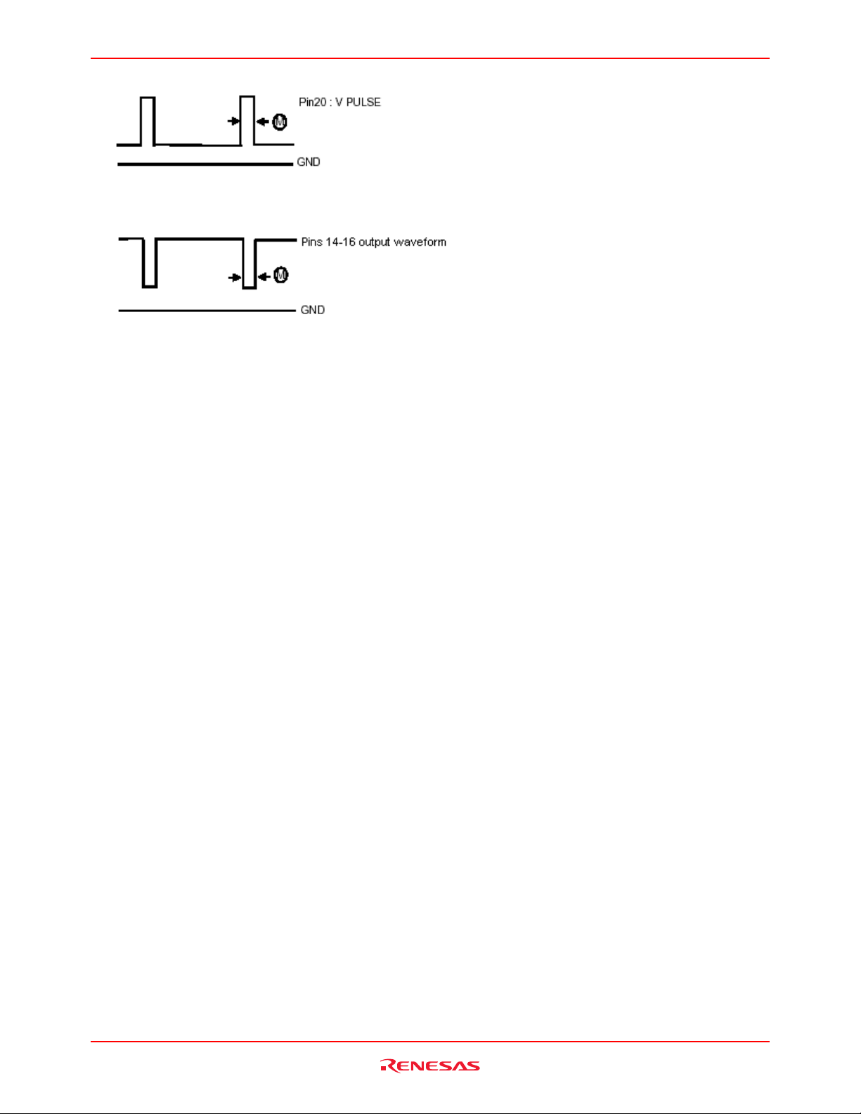
• HPT1: Horizontal pulse timing 1
• HPT2: Horizontal pulse timing 2
1. Measure the horizontal pulse timing using the method for HPT1.
2. Typical
HPT2 = (measured value) - HPT1
• HPTW: Horizontal pulse width
• VH: Horizontal pulse amplitude
Rev.1.0, Sep.23.2003, page 44 of 49
Page 45

M61250BFP
• HSTA: Horizontal pulse stop operation
Confirm that when H.START SW OFF (0FH:D7=0), the horizontal output goes low.
• AFCG: AFC gain operation
1. Measure the pin 7 output amplitude during AFC switching, taking the result during SW ON to be AFCon, and
during SW OFF to be AFCoff.
2. AFCG is defined as follows.
• fV: Vertical free-running frequency
Measure the pin 5 output frequency with no input.
• Vfree: Forced vertical free-running operation
1. Input SG.A to pin 38.
2. Set V-FREE CONTROL DATA to on, measure the pin 5 output amplitude.
• SCV: Service mode operation
Measure the pin 5 output DC voltage with the service switch on.
• FPVU: Vertical pull-in frequency (upper)
• FVPL: Vertical pull-in frequency (lower)
Change the SG.H vertical frequency, and measure the frequency when the pin 5 output waveform is pulled in.
• VRsi: Vertical ramp size
• VRsc1: Vertical ramp size control range 1
• VRsc2: Vertical ramp size control range 2
• VRpo1: Vertical ramp position control range 1
• VRpo2: Vertical ramp position control range 2
1. Measure the vertical ramp timing using the same method as for VRpo1.
2. VRpo2 is defined as follows.
VRpo2 = (measured value) –VRpo1
Rev.1.0, Sep.23.2003, page 45 of 49
Page 46
M61250BFP
• VW: Vertical pulse width
• VBLKW: Vertical BLK width
• WVSS: Minimum width at minimum sync oper ation
Reduce the width of the SG.I signal, and measure the input signal width when the pin 5 output waveform pull-in is lost.
Rev.1.0, Sep.23.2003, page 46 of 49
Page 47

M61250BFP
5
The following function is added to the M61250BFP (VBLKWVS1 to VBLKWVS3)
The vertical blanking width can be specified independently of VSHIFT.
Note, however, that it operates in the same way as conventional products in the initial state.
The following bits are added to the I
2
C register.
• VBLK SHIFT ON (1CH D3) Initial value = 0
0: Shifts the VBLK based on the conventional SHIFT
1: Shifts the VBLK based on the VBLK SHIFT.
• VBLK SHIFT (1CH D2 to 1CH D0) Initial value = 4
0: VBLK period is 260 H to 21 H.
1: VBLK period is 260 H to 21 H.
2: VBLK period is 260 H to 23 H.
3: VBLK period is 260 H to 25 H.
4: VBLK period is 260 H to 27 H.
5: VBLK period is 260 H to 29 H.
6: VBLK period is 260 H to 31 H.
7: VBLK period is 260 H to 33 H.
Vertical
Imaging
period
525524
523
VOUT(VSHIFT based shift)
Equivalent
12345 6 7
pulse
synchronization
Equivalent
pulse
91011 12 20 21
8
23
25 27 29 31
Imaging period
3
33
VBLK
(VBLK
SHIFT=0)
(VBLK
SHIFT=1)
(VBLK
SHIFT=2)
(VBLK
SHIFT=3)
(VBLK
SHIFT=4)
(VBLK
SHIFT=5)
(VBLK
SHIFT=6)
(VBLK
SHIFT=7)
• An image may be output during the V blanking period according to the VSHIFT value.
In this case, the VBLK should be shifted in order not to output the image during the blanking period. Carefully
consider this because the output condition chang e s according to the circuit connected externally.
Rev.1.0, Sep.23.2003, page 47 of 49
Page 48

M61250BFP
Important Information
• Each application should be thoroughly studied and evaluated before making a decision.
• 47 mF and higher electrolytic capacitors and 0.01 mF and higher ceramic capacitors should be connected in parallel
between each of the power supply pins (3, 4, 12, 39 , 42, 44) and ground pin. In addition, it is recommen ded that the
connectors be made as close to the IC power supply pins as possible.
• The C-SYNC output operation of the intelligent monitor (18 pins) cannot be guaranteed at Hfree (13H: D7 = 1) .
• When purchasing I2C bus components, a license to use these components within a 12C bus system is provided
under the 12C patent rights of Philips Corp.
However, the bus system must conform to the 12C specifications stipulated by Philips.
Rev.1.0, Sep.23.2003, page 48 of 49
Page 49

M61250BFP
Package Dimensions
D
M
—
1.0
—
1
L
0.75
0.6
A3
Lp 0.45
—
0.25
—
0.2
—
—
x
0.1
—
—
y
14.113.9
14.0
D
14.113.9
0.8
14.0
e
E
—
—
16.215.8
16.0
D
H
0.70.50.3
16.215.8
16.0
E
L
H
—
1.7
M
E
—
—
Min Nom Max
e
b
2
2
l
Dimension in Millimeters
Recommended Mount Pad
A
0.2
0.1
0
1
A
1.4
—
2
A
0.450.370.32
b
0.1750.1250.105
c
—
0˚ 8˚
——
0.5
2
b
——
0.95
2
I
——
14.4
D
M
——
14.4
E
M
Symbol
c
A3
1
A
L
L
Lp
Cu Alloy
Lead Material
Weight(g)
—
JEDEC Code
MMP
Detail F
A
1
M
48
A
2
H
E
E
33
F
x
b
D
D
H
y
e
64 49
1
17 32
16
EIAJ Package Code
LQFP64-P-1414-0.8
64P6U-A Plastic 64pin 14 14mm body LQFP
Rev.1.0, Sep.23.2003, page 49 of 49
Page 50

©
.
!
y
may
.
gy
.
7
b
y
.
.
S
ales Strategic Planning Div. Nippon Bldg., 2-6-2, Ohte-machi, Chiyoda-ku, Tokyo 100-0004, Japa
n
m
Keep safety first in your circuit designs
1. Renesas Technology Corp. puts the maximum effort into making semiconductor products better and more reliable, but there is alwa
occur with them. Trouble with semiconductors may lead to personal injury, fire or property damage
Remember to give due consideration to safety when making your circuit designs, with appropriate measures such as (i) placement of substitutive, auxiliary
circuits, (ii) use of nonflammable material or (iii) prevention against any malfunction or mishap.
Notes regarding these materials
1. These materials are intended as a reference to assist our customers in the selection of the Renesas Technology Corp. product best suited to the customer's
application; they do not convey any license under any intellectual property rights, or any other rights, belonging to Renesas Technology Corp. or a third party.
2. Renesas Technology Corp. assumes no responsibility for any damage, or infringement of any third-party's rights, originating in the use of any product data,
diagrams, charts, programs, algorithms, or circuit application examples contained in these materials.
3. All information contained in these materials, including product data, diagrams, charts, programs and algorithms represents information on products at the time of
publication of these materials, and are subject to change by Renesas Technology Corp. without notice due to product improvements or other reasons. It is
therefore recommended that customers contact Renesas Technology Corp. or an authorized Renesas Technology Corp. product distributor for the latest product
information before purchasing a product listed herein.
The information described here may contain technical inaccuracies or typographical errors.
Renesas Technology Corp. assumes no responsibility for any damage, liability, or other loss rising from these inaccuracies or errors.
Please also pay attention to information published by Renesas Technology Corp. by various means, including the Renesas Technology Corp. Semiconductor
home page (http://www.renesas.com).
4. When using any or all of the information contained in these materials, including product data, diagrams, charts, programs, and algorithms, please be sure to
evaluate all information as a total system before making a final decision on the applicability of the information and products. Renesas Technology Corp. assumes
no responsibility for any damage, liability or other loss resulting from the information contained herein.
5. Renesas Technology Corp. semiconductors are not designed or manufactured for use in a device or system that is used under circumstances in which human life
is potentially at stake. Please contact Renesas Technology Corp. or an authorized Renesas Technology Corp. product distributor when considering the use of a
product contained herein for any specific purposes, such as apparatus or systems for transportation, vehicular, medical, aerospace, nuclear, or undersea repeater
use.
6. The prior written approval of Renesas Technolo
. If these products or technologies are subject to the Japanese export control restrictions, they must be exported under a license from the Japanese government and
cannot
An
8. Please contact Renesas Technology Corp. for further details on these materials or the products contained therein
e imported into a country other than the approved destination.
diversion or reexport contrary to the export control laws and regulations of Japan and/or the country of destination is prohibited
Corp. is necessary to reprint or reproduce in whole or in part these materials
s the possibility that trouble
RENESAS SALES OFFICES
Renesas Technology America, Inc.
450 Holger Way, San Jose, CA 95134-1368, U.S.A
Tel: <1> (408) 382-7500 Fax: <1> (408) 382-7501
Renesas Technology Europe Limited.
Dukes Meadow, Millboard Road, Bourne End, Buckinghamshire, SL8 5FH, United Kingdom
Tel: <44> (1628) 585 100, Fax: <44> (1628) 585 900
Renesas Technology Europe GmbH
Dornacher Str. 3, D-85622 Feldkirchen, Germany
Tel: <49> (89) 380 70 0, Fax: <49> (89) 929 30 11
Renesas Technology Hong Kong Ltd.
7/F., North Tower, World Finance Centre, Harbour City, Canton Road, Hong Kong
Tel: <852> 2265-6688, Fax: <852> 2375-6836
Renesas Technology Taiwan Co., Ltd.
FL 10, #99, Fu-Hsing N. Rd., Taipei, Taiwan
Tel: <886> (2) 2715-2888, Fax: <886> (2) 2713-2999
Renesas Technology (Shanghai) Co., Ltd.
26/F., Ruijin Building, No.205 Maoming Road (S), Shanghai 200020, China
Tel: <86> (21) 6472-1001, Fax: <86> (21) 6415-2952
Renesas Technology Singapore Pte. Ltd.
1, Harbour Front Avenue, #06-10, Keppel Bay Tower, Singapore 098632
Tel: <65> 6213-0200, Fax: <65> 6278-8001
2003. Renesas Technology Corp., All rights reserved. Printed in Japan
http://www.renesas.co
Colophon 1.0
 Loading...