

Page 1
查询M5M29KE131BVP供应商
Preliminary
Notice: This is not a final specification.
Some parametric limits are subject to change.
134,217,728-BIT (16,777,216-WORD BY 8-BIT / 8,388,608-WORD BY 16-BIT)
DESCRIPTION
The M5M29KE131BVP is a Stacked micro Multi Chip
Package that contents 2 Dies of 64M-bit Flash memory in a
48-pin TSOP(I) for lead free use.
128M-bit Flash memory is a 16,777,216 bytes / 8,388,608
words, single power supply and high performance nonvolatile memory fabricated by CMOS technology for the
peripheral circuit and DINOR IV (Divided bit-line NOR IV)
architecture for the memory cell. All memory blocks are
locked and can not be programmed or erased, when WP# is
Low. Using Software Lock Release function, program or
erase operation can be executed.
Renesas LSIs
M5M29KE131BVP
CMOS FLASH MEMORY
Stacked-uMCP (micro Multi Chip Package)
The M5M29KE131BVP is suitable for a high performance cellular
phone and a mobile PC that are required to be small mounting
area, weight and small power dissipation.
FEATURES
Access time Random 70ns (Max.)
Page 25ns(Max.)
Supply voltage VCC= 3.0 ~ 3.6V
Ambient temperature Ta=-40 ~ 85 °C
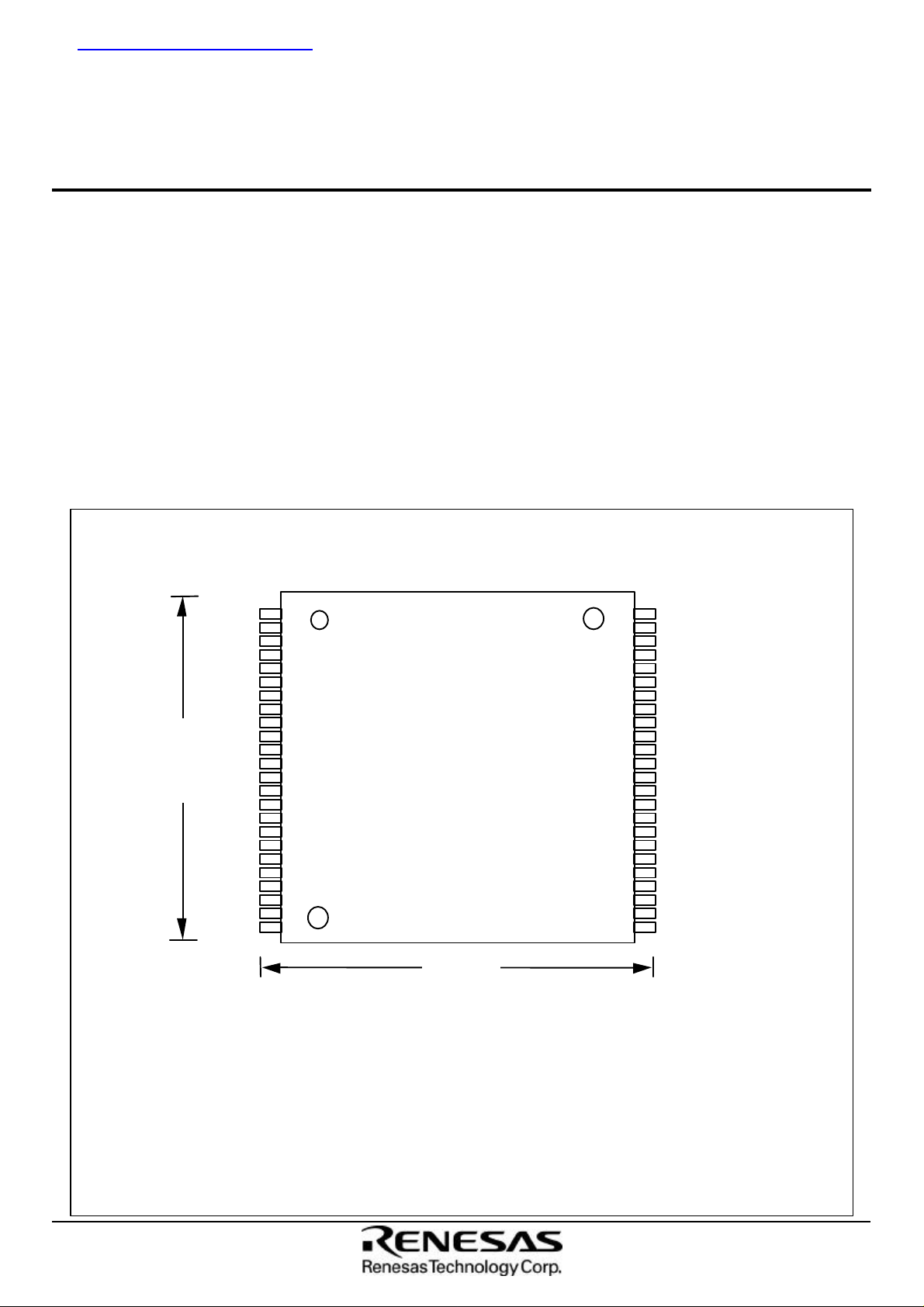
Package 48pin TSOP(Type-I), Lead pitch 0.5mm
Outer-lead finishing : Sn-Cu
APPLICATION
Digital Cellar Phone, Telecommunication,
PDA, Car Navigation System, Video Game Machine
12.0 mm
A15
A14
A13
A12
A11
A10
A9
A8
A19
A20
WE#
RP#
A21
WP#
A22#
A18
A17
A7
A6
A5
A4
A3
A2
A1
PIN CONFIGURATION (TOP VIEW)
1
2
3
4
5
6
7
8
9
10
11
12
13
14
15
16
17
18
19
20
21
22
23
24
M5M29KE131BVP
20.0 mm
48
47
46
45
44
43
42
41
40
39
38
37
36
35
34
33
32
31
30
29
28
27
26
25
A16
BYTE#
GND
DQ15/A-1
DQ7
DQ14
DQ6
DQ13
DQ5
DQ12
DQ4
VCC
DQ11
DQ3
DQ10
DQ2
DQ9
DQ1
DQ8
DQ0
OE#
GND
CE#
A0
Outline
48P3R-C
VCC : VCC
GND : GND
A0-A22 : Address
DQ0-DQ15 : Data I/O
CE# : Chip enable
OE# : Output enable
1
WE# : Write enable
WP# : Write protect
RP# : Reset power down
BYTE# : Byte enable
Rev.0.2_48a_bezz
Page 2
Preliminary
Input
A22-A0, OE#, WE#, CE#, WP#,
Output
Notice: This is not a final specification.
Some parametric limits are subject to change.
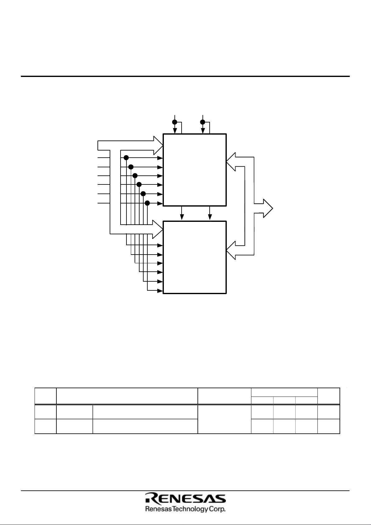
MCP Block Diagram
A0 to A22
CE#
WP#
RP#
WE#
OE#
BYTE#
Renesas LSIs
M5M29KE131BVP
134,217,728-BIT (16,777,216-WORD BY 8-BIT / 8,388,608-WORD BY 16-BIT)
CMOS FLASH MEMORY
Stacked-uMCP (micro Multi Chip Package)
Vcc GND
64Mbit DINOR IV
Flash Memory
DQ0 to DQ15
64Mbit DINOR IV
Flash Memory
Capacitance
Symbol Conditions
CIN
COUT
capacitance
Capacitance
RP#,BYTE#
Parameter
Ta=25°C, f=1MHz,
DQ15-DQ0 24 pF
Vin=Vout=0V
Limits
Min. Typ. Max.
24 pF
Unit
2
Rev.0.2_48a_bezz
Page 3

Preliminary
Notice: This is not a final specification.
Some parametric limits are subject to change.
Flash Memory Part
Renesas LSIs
M5M29KE131BVP
134,217,728-BIT (16,777,216-WORD BY 8-BIT / 8,388,608-WORD BY 16-BIT)
CMOS FLASH MEMORY
Stacked-uMCP (micro Multi Chip Package)
Description
The 128M-bit DINOR IV(Divided bit line NOR IV) Flash
Memory is 3.3V-only high speed 134,217,728-bit CMOS
boot block Flash Memory. Alternating BGO(Back Ground
Operation) feature of the device allows Program or Erase
operations to be performed in one bank while the device
simultaneously allows Read operations to be performed
on the other bank in each 64M-bit area which is selected
by A22=L or H. This BGO feature is suitable for
communication products and cellular phone.The Flash
Memory is fabricated by CMOS technology for the
peripheral circuits and DINOR IV architecture for the
memory cells.
Features
- Organization 8,388,608-word x 16-bit
16,777,216-word x 8-bit
- Supply Voltage VCC = 3.0 ~ 3.6V
- Access time
Random Access 70ns(Max.)
Random Page Read 25ns(Max.)
- Read 108mW (Max. at 5MHz)
- Page Read 36mW (Max.)
(After Automatic Power Down) 0.66µW(typ.)
- Program/Erase 126mW(Max.)
Standby 0.66µW(typ.)
Deep Power Down mode 0.66µW(typ.)
- Auto Program for Bank(I) – Bank(IV)
Program Time
Word Program 30µs/1word(typ.)
Byte Program 30µs/1byte(typ.)
Page Program 4ms(typ.)
Program Unit
Word Program 1 word
Byte Program 1 byte
Page Program 128 words/256 bytes
- Auto Erase
Erase time 150ms(typ.)
Erase unit
Bank(I) ,Bank(VIII)
Boot Block 4K-word /8K-byte x 2
Parameter Block 4K-word /8K-byte x 6
Main Block 32K-word /64K-byte x 7
Bank(II) ,Bank(VII)
Main Block 32K-word /64K-byte 8
Bank(III) ,Bank(VI)
Main Block 32K-word /64K-byte x 56
Bank(IV) ,Bank(V)
Main Block 32K-word /64K-byte x 56
- Program/Erase cycles 100Kcycles
- Dual Boot Block Architecture
There are Bottom and Top boot blocks in both sides.
Bottom Boot (A22=VIL )
Top Boot (A22=VIH)
- The Other Functions
Software Command Control
Quick Data Reclaim
Software Lock Release(while WP# is low)
Erase Suspend/Resume
Program Suspend/Resume
Status Register Read
Alternating Back Ground Program/Erase Operation
Among Bank (I)-Bank(IV)
in Bottom 64Mbit area (A22=VIL),
Among Bank (V)-Bank(VIII)
in Top 64Mbit area (A22=VIH)
Random Page Read
3
Rev.0.2_48a_bezz
Page 4
Preliminary
Boot Block T134 4Kword
.
Boot Block T133 4Kword
.
Parameter Block T132 4Kword
.
Bank(VIII)
..15blocks
Parameter Block T127 4Kword
.
Main Block T126 32Kword
...
Main Block T120 32Kword
.
Main Block T119 32Kword
.
Bank(VII)
..8blocks
..Main Block T112 32Kword
.
Main Block T111 32Kword
.
Bank(VI)
..56blocks
..Main Block T56 32Kword
.
Main Block T55 32Kword
.
Bank(V)
..56blocks
.
Main Block T0 32Kword
Main Block B134 32Kword
.
Bank(IV)
..56blocks
..Main Block B79 32Kword
.
Main Block B78 32Kword
.
Bank(III)
..56blocks
..Main Block B23 32Kword
.
Main Block B22 32Kword
.
Bank(II)
..8blocks
..Main Block B15 32Kword
.
Main Block B14 32Kword
...
Main Block B8 32Kword
.
Bank(I)
Parameter Block B7 4Kword
.
15blocks
..Parameter Block B2 4Kword
.
Boot Block B1 4Kword
Boot Block B0 4Kword
.....
128word Page Buffer
……………………
Notice: This is not a final specification.
Some parametric limits are subject to change.
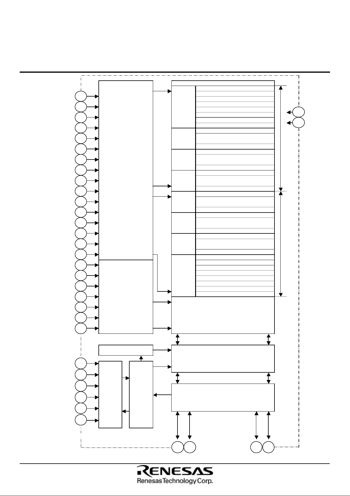
Block Diagram
(128Mbit Flash Memory)
A22
Renesas LSIs
M5M29KE131BVP
134,217,728-BIT (16,777,216-WORD BY 8-BIT / 8,388,608-WORD BY 16-BIT)
CMOS FLASH MEMORY
Stacked-uMCP (micro Multi Chip Package)
Address
Input
A21
A20
A19
A18
A17
A16
A15
A14
A13
A12
A11
A10
A9
A8
A7
A6
A5
VCC
GND
A22="H"A22="L"
X-Decoder
Chip
Enable
Output Enable
Write Enable
Write
Protect
Reset
/PowerDown
BYTE
Enable
A4
A3
A2
A1
A0
F-CE#
OE#
WE#
F-WP#
F-RP#
BYTE#
Y-Decoder
Status / ID Register
Command
User
Interface
Write
State
Machine
DQ15
/A-1
Y-Gate / Sense Amp.
………………………………….
Multiplexer
………………………………….
I/O Buffer
……………………
Data I/O
DQ14
DQ0DQ1
4
Rev.0.2_48a_bezz
Page 5

Preliminary
Notice: This is not a final specification.
Some parametric limits are subject to change.
Renesas LSIs
M5M29KE131BVP
134,217,728-BIT (16,777,216-WORD BY 8-BIT / 8,388,608-WORD BY 16-BIT)
CMOS FLASH MEMORY
Stacked-uMCP (micro Multi Chip Package)
Function of Flash Memory
The 128M-bit DINOR IV Flash Memory includes on-chip
program/erase control circuitry. The Write State Machine
(WSM) controls block erase and word/page program
operations. Operational modes are selected by the
commands written to the Command User Interface (CUI).
The Status Register indicates the status of the WSM and
when the WSM successfully completes the desired
program or block erase operation.
A Deep Power Down mode is enabled when the RP# pin
is at GND, minimizing power consumption.
Read
The 128M-bit DINOR IV Flash Memory has four read
modes, which accesses to the memory array ,the Page read,
the Device Identifier and the Status Register. The
appropriate read commands are required to be written to the
CUI. Upon initial device power up or after exit from deep
power down, the 128M-bit DINOR IV Flash Memory
automatically resets to read array mode. In the read array
mode and in the conditions are low level input to OE#, high
level input to WE# and RP#, low level input to CE# and
address signals to the address inputs (A22 - A0:Word Mode,
A22-A-1:Byte Mode) the data of the addressed location to
the data input/output (DQ15-DQ0:Word Mode, DQ7DQ0:Byte Mode) is output.
Output Disable
When OE# is at VIH, output from the devices is disabled.
Data input/output are in a high-impedance (High-Z) state.
Standby
When CE# is at VIH, the device is in the standby mode
and its power consumption is reduced. Data input/output
are in a high-impedance (High-Z) state. If the memory is
deselected during block erase or program, the internal
control circuits remain active and the device consumes
normal active power until the operation completes.
Deep Power Down
When RP# is at VIL, the device is in the deep power down
mode and its power consumption is substantially low.
During read modes, the memory is deselected and the data
input/output are in a high-impedance (High-Z) state. After
return from power down, the CUI is reset to Read Array,
and the Status Register is cleared to value 80H.
During block erase or program modes, RP# low will abort
either operation. Memory array data of the block being
altered become invalid.
Automatic Power Down (Auto-PD)
Write
Writes to the CUI enables reading of memory array data,
device identifiers and reading and clearing of the Status
Register. They also enable block erase and program. The
CUI is written by bringing WE# to low level and OE# is at
high level, while CE# is at low level. Address and data are
latched on the earlier rising edge of WE# and CE#.
Standard micro processor write timings are used.
Alternating Background Operation (BGO)
The 128M-bit DINOR IV Flash Memory allows to read array
from one bank while the other bank operates in software
command write cycling or the erasing / programming
operation in the background. Array Read operation with the
other bank in BGO is performed by changing the bank
address without any additional command. When the bank
address points the bank in software command write cycling
or the erasing / programming operation, the data is read out
from the status register. The access time with BGO is the
same as the normal read operation.
The Automatic Power Down minimizes the power
consumption during read mode. The device automatically
turns to this mode when any addresses or CE# isn't
changed more than 200ns after the last alternation. The
power consumption becomes the same as the stand-by
mode. During this mode, the output data is latched and can
be read out. New data is read out correctly when
addresses are changed.
BBR(Back Bank array Read)
In the 128M-bit DINOR IV Flash Memory , when one
memory address is read according to a Read Mode in the
case of the same as an access when a Read Mode
command is input, an another Bank memory data can be
read out (Read Array or Page Read) by changing an
another Bank address.
5
Rev.0.2_48a_bezz
Page 6

Preliminary
Notice: This is not a final specification.
Some parametric limits are subject to change.
Renesas LSIs
M5M29KE131BVP
134,217,728-BIT (16,777,216-WORD BY 8-BIT / 8,388,608-WORD BY 16-BIT)
CMOS FLASH MEMORY
Stacked-uMCP (micro Multi Chip Package)
Software Command Definitions
The device operations are selected by writing specific
software command into the Command User Interface.
Clear Status Register Command (50H)
The Erase Status, Program Status and Block Status bits
are set to "1"s by the Write State Machine and can only
be reset by the Clear Status Register command of 50H.
These bits indicate various failure conditions.
Read Array Command (FFH)
The device is in Read Array mode on initial device power
up and after exit from deep power down, or by writing FFH
to the Command User Interface. After starting the internal
operation the device is set to the read status register mode
automatically. Automated block erase is initiated by writing the Block
Read Device Identifier Command (90H)
We can normally read device identifier codes when Read
Device Identifier Code Command (90H) is written to the
command latch. Following the command write, the
manufacturer code and the device code can be read from
A0 address 0H and 1H in a bank address, respectively.
Read Status Register Command (70H)
The Status Register is read after writing the Read Status
Register command of 70H to the Command User Interface.
Also, after starting the internal operation the device is set to
the Read Status Register mode automatically.
The contents of Status Register are latched on the later
falling edge of OE# must be toggled every status read.
Block Erase / Confirm Command (20H/D0H)
Erase command of 20H followed by the Confirm
command of D0H. An address within the block to be
erased is required. The WSM executes iterative erase
pulse application and erase verify operation.
Program Commands
A) Word / Byte Program (40H)
Word/Byte program is executed by a two-command
sequence. The Word/Byte program Setup command of
40H is written to the Command Interface, followed by a
second write specifying the address and data to be written.
The WSM controls the program pulse application and
verify operation.
Page Read Command (F3H)
The Page Read command (F3H) timing can be used by
writing the first command to CUI and F-CE# falls VIL or
changing the address(A22-A2) is necessary to start
activating page read mode. This command is fast random
4 words read. During the read it is necessary to fix F-CE#
low and change addresses that are defined by A0 and
A1(0h - 3h) at random continuously. The mode is kept until
F-RP# is set to L or this chip is powered down.
The first read of Page Read timing is the same as normal
read (ta(CE)). F-CE# should be fallen “L”. The read timing
after the first is the same as ta(PAD).
In the page read mode the upper address(A22-A2) or FCE# are supposed not to be clocked during read operation.
Otherwise the access time is as same as normal read.
B) Page Program for Data Blocks (41H)
Page Program allows fast programming of 128words
/256bytes of data. Writing of 41H initiates the page
program operation for the Data area. From 2nd cycle to
129th cycle :Word Mode, 257th cycle :Byte Mode, write
data must be serially inputted. Address A6-A0:Word
Mode, A6-A-1:Byte Mode have to be incremented from
00H to 7FH. After completion of data loading, the WSM
controls the program pulse application and verify
operation.
C) Single Data Load to Page Buffer (74H)
/ Page Buffer to Flash (0EH/D0H)
Single data load to the page buffer is performed by
writing 74H followed by a second write specifying the
column address(A6-A0:Word Mode, A6-A-1:Byte Mode)
and data. Distinct data up to 128word/256bytes can be
loaded to the page buffer by this two-command sequence.
On the other hand, all of the loaded data to the page buffer
is programmed simultaneously by writing Page Buffer to
Flash command of 0EH followed by the confirm command
of D0H. After completion of programming the data on the
page buffer is cleared automatically.
6
Rev.0.2_48a_bezz
Page 7

Preliminary
Notice: This is not a final specification.
Some parametric limits are subject to change.
134,217,728-BIT (16,777,216-WORD BY 8-BIT / 8,388,608-WORD BY 16-BIT)
Flash to Page Buffer Command (F1H/D0H) Power Supply Voltage
M5M29KE131BVP
Stacked-uMCP (micro Multi Chip Package)
Renesas LSIs
CMOS FLASH MEMORY
Array data load to the page buffer is performed by
writing the Flash to Page Buffer command of F1H
followed by the Confirm command of D0H. An address
within the page to be loaded is required. Then the array
data can be copied into the other pages within the same
bank by using the Page Buffer to Flash command.
Clear Page Buffer Command (55H/D0H)
Loaded data to the page buffer is cleared by writing the
Clear Page Buffer command of 55H followed by the
Confirm command of D0H. This command is valid for
clearing data loaded by Single Data Load to Page Buffer
command.
Data Protection
The 128M-bit DINOR IV Flash Memory has a master
Write Protect pin (WP#). When WP# is at VIH, all blocks
can be programmed or erased. When WP# is low, all
blocks are in locked mode which prevents any
modifications to memory blocks. Software Lock Release
function is only command which allows to program or erase.
When the power supply voltage is less than VLKO, Low
VCC Lock-Out voltage, the device is set to the Read-only
mode.
A delay time of 60µs is required before any device
operation is initiated. The delay time is measured from the
time Flash VCC reaches Flash VCCmin (3.0V).
During power up, RP# = GND is recommended. Falling in
Busy status is not recommended for possibility of
damaging the device.
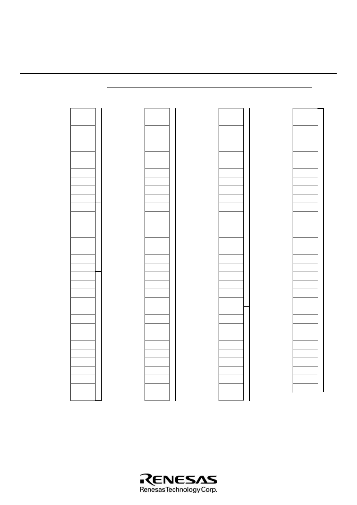
Memory Organization
The 128M-bit DINOR IV Flash Memory is constructed by
2 boot blocks of 4K words, 6 parameter blocks of 4K words
and 7 main blocks of 32K words in Bank(I) and Bank(VIII),
by 8 main blocks of 32K words in Bank(II) and Bank(VII),
and by 56 main blocks of 32K words in Bank(III),
BANK(IV) , BANK(V) and Bank(VI).
A block is erased independently of other blocks in the
array.
Suspend/Resume Command (B0H/D0H)
Writing the Suspend command of B0H during block erase
operation interrupts the block erase operation and allows
read out from another block of memory. Writing the
Suspend command of B0H during program operation
interrupts the program operation and allows read out from
another block of memory. The Bank address is required
when writing the Suspend/Resume Command. The device
continues to output Status Register data when read, after
the Suspend command is written to it. Polling the WSM
Status and Suspend Status bits will determine when the
erase operation or program operation has been suspended.
At this point, writing of the Read Array command to the CUI
enables reading data from blocks other than that which is
suspended. When the Resume command of D0H is written
to the CUI, the WSM will continue with the erase or
program processes.
Erase All Unlocked Blocks Command (A7H/D0H)
The command sequence enable us to erase all blocks.
The command can be used by writing Setup command
A7H(1stcycle) and confirm command D0H(2ndcycle). The
sequence is not valid in case of WP#=VIL.
7
Rev.0.2_48a_bezz
Page 8
Preliminary
Notice: This is not a final specification.
Some parametric limits are subject to change.
Renesas LSIs
M5M29KE131BVP
134,217,728-BIT (16,777,216-WORD BY 8-BIT / 8,388,608-WORD BY 16-BIT)
CMOS FLASH MEMORY
Stacked-uMCP (micro Multi Chip Package)
Block Organization
x8 (Byte
x16 (Word
Mode)
1A0000H1AFFFFH
190000H19FFFFH
180000H18FFFFH
170000H17FFFFH
160000H16FFFFH
150000H15FFFFH
140000H14FFFFH
130000H13FFFFH
120000H12FFFFH
110000H11FFFFH
100000H10FFFFH
F0000HFFFFFH
E0000HEFFFFH
D0000HDFFFFH
C0000HCFFFFH
B0000HBFFFFH
A0000HAFFFFH
90000H9FFFFH
80000H8FFFFH
70000H7FFFFH
60000H6FFFFH
50000H5FFFFH
40000H4FFFFH
30000H3FFFFH
20000H2FFFFH
10000H1FFFFH
0E000H0FFFFH
0C000H0DFFFH
0A000H0BFFFH
08000H09FFFH
06000H07FFFH
04000H05FFFH
02000H03FFFH
00000H01FFFH
Mode)
D0000HD7FFFH 32Kword 33
C8000HCFFFFH 32Kword 32
C0000HC7FFFH
B8000HBFFFFH 32Kword 30
B0000HB7FFFH 32Kword 29
A8000HAFFFFH 32Kword 28
A0000HA7FFFH 32Kword 27
98000H9FFFFH
90000H97FFFH 32Kword 25
88000H8FFFFH 32Kword 24
80000H87FFFH 32Kword 23
78000H7FFFFH
70000H77FFFH 32Kword 21
68000H6FFFFH 32Kword 20
60000H67FFFH 32Kword 19
58000H5FFFFH 32Kword 18
50000H57FFFH
48000H4FFFFH 32Kword 16
40000H47FFFH 32Kword 15
38000H3FFFFH 32Kword 14
30000H37FFFH
28000H2FFFFH 32Kword 12
20000H27FFFH 32Kword 11
18000H1FFFFH 32Kword 10
10000H17FFFH
08000H0FFFFH 32Kword 8
07000H07FFFH 4Kword 7
06000H06FFFH 4Kword 6
05000H05FFFH 4Kword 5
04000H04FFFH
03000H03FFFH 4Kword 3
02000H02FFFH 4Kword 2
01000H01FFFH 4Kword 1
00000H00FFFH
A21-A-1
A21-A0
(Byte
(Word
Mode)
Mode)
32Kword 31
32Kword 26
32Kword 22
32Kword 17
32Kword 13
32Kword 9
4Kword 4
4Kword 0
128M-bit DINOR(IV) Flash Memory Map (Bottom 64Mbit / A22=VIL)
x8 (Byte
Mode)
3C0000H3CFFFFH
3B0000H3BFFFFH
3A0000H3AFFFFH
390000H39FFFFH
380000H38FFFFH
370000H37FFFFH
360000H36FFFFH
350000H35FFFFH
340000H34FFFFH
330000H33FFFFH
320000H32FFFFH
310000H31FFFFH
300000H30FFFFH
2F0000H2FFFFFH
2E0000H2EFFFFH
2D0000H2DFFFFH
2C0000H2CFFFFH
2B0000H2BFFFFH
2A0000H2AFFFFH
290000H29FFFFH
280000H28FFFFH
270000H27FFFFH
260000H26FFFFH
250000H25FFFFH
BANK(I)BANK(II)BANK(III)
240000H24FFFFH
230000H23FFFFH
220000H22FFFFH
210000H21FFFFH
200000H20FFFFH
1F0000H1FFFFFH
1E0000H1EFFFFH
1D0000H1DFFFFH
1C0000H1CFFFFH
1B0000H1BFFFFH
A21-A-1
(Byte
Mode)
x16 (Word
Mode)
1E0000H1E7FFFH 32Kword 67
1D8000H1DFFFFH 32Kword 66
1D0000H1D7FFFH
32Kword 65
1C8000H1CFFFFH 32Kword 64
1C0000H1C7FFFH 32Kword 63
1B8000H1BFFFFH 32Kword 62
1B0000H1B7FFFH 32Kword 61
1A8000H1AFFFFH
32Kword 60
1A0000H1A7FFFH 32Kword 59
198000H19FFFFH 32Kword 58
190000H197FFFH 32Kword 57
188000H18FFFFH
32Kword 56
180000H187FFFH 32Kword 55
178000H17FFFFH 32Kword 54
170000H177FFFH 32Kword 53
168000H16FFFFH 32Kword 52
160000H167FFFH
32Kword 51
158000H15FFFFH 32Kword 50
150000H157FFFH 32Kword 49
148000H14FFFFH 32Kword 48
140000H147FFFH
32Kword 47
138000H13FFFFH 32Kword 46
130000H137FFFH 32Kword 45
128000H12FFFFH 32Kword 44
120000H127FFFH
32Kword 43
118000H11FFFFH 32Kword 42
110000H117FFFH 32Kword 41
108000H10FFFFH 32Kword 40
100000H107FFFH 32Kword 39
F8000HFFFFFH
32Kword 38
F0000HF7FFFH 32Kword 37
E8000HEFFFFH 32Kword 36
E0000HE7FFFH 32Kword 35
D8000HDFFFFH
32Kword 34
A21-A0
(Word
Mode)
x8 (Byte
Mode)
5E0000H5EFFFFH
5D0000H5DFFFFH
5C0000H5CFFFFH
5B0000H5BFFFFH
5A0000H5AFFFFH
590000H59FFFFH
580000H58FFFFH
570000H57FFFFH
560000H56FFFFH
550000H55FFFFH
540000H54FFFFH
530000H53FFFFH
520000H52FFFFH
510000H51FFFFH
BANK(III)
500000H50FFFFH
4F0000H4FFFFFH
4E0000H4EFFFFH
4D0000H4DFFFFH
4C0000H4CFFFFH
4B0000H4BFFFFH
4A0000H4AFFFFH
490000H49FFFFH
480000H48FFFFH
470000H47FFFFH
460000H46FFFFH
450000H45FFFFH
440000H44FFFFH
430000H43FFFFH
420000H42FFFFH
410000H41FFFFH
400000H40FFFFH
3F0000H3FFFFFH
3E0000H3EFFFFH
3D0000H3DFFFFH
A21-A-1
(Byte
Mode)
x16 (Word
Mode)
2F0000H2F7FFFH 32Kword 101
2E8000H2EFFFFH 32Kword 100
2E0000H2E7FFFH
32Kword 99
2D8000H2DFFFFH 32Kword 98
2D0000H2D7FFFH 32Kword 97
2C8000H2CFFFFH 32Kword 96
2C0000H2C7FFFH 32Kword 95
2B8000H2BFFFFH
32Kword 94
2B0000H2B7FFFH 32Kword 93
2A8000H2AFFFFH 32Kword 92
2A0000H2A7FFFH 32Kword 91
298000H29FFFFH
32Kword 90
290000H297FFFH 32Kword 89
288000H28FFFFH 32Kword 88
280000H287FFFH 32Kword 87
278000H27FFFFH 32Kword 86
270000H277FFFH
32Kword 85
268000H26FFFFH 32Kword 84
260000H267FFFH 32Kword 83
258000H25FFFFH 32Kword 82
250000H257FFFH
32Kword 81
248000H24FFFFH 32Kword 80
240000H247FFFH 32Kword 79
238000H23FFFFH 32Kword 78
230000H237FFFH
32Kword 77
228000H22FFFFH 32Kword 76
220000H227FFFH 32Kword 75
218000H21FFFFH 32Kword 74
210000H217FFFH 32Kword 73
208000H20FFFFH
32Kword 72
200000H207FFFH 32Kword 71
1F8000H1FFFFFH 32Kword 70
1F0000H1F7FFFH 32Kword 69
1E8000H1EFFFFH
32Kword 68
A21-A0
(Word
Mode)
x8 (Byte
Mode)
7F0000H7FFFFFH
7E0000H7EFFFFH
7D0000H7DFFFFH
7C0000H7CFFFFH
7B0000H7BFFFFH
7A0000H7AFFFFH
790000H79FFFFH
780000H78FFFFH
770000H77FFFFH
760000H76FFFFH
750000H75FFFFH
740000H74FFFFH
730000H73FFFFH
720000H72FFFFH
BANK(IV)
710000H71FFFFH
700000H70FFFFH
6F0000H6FFFFFH
6E0000H6EFFFFH
6D0000H6DFFFFH
6C0000H6CFFFFH
6B0000H6BFFFFH
6A0000H6AFFFFH
690000H69FFFFH
680000H68FFFFH
670000H67FFFFH
660000H66FFFFH
650000H65FFFFH
640000H64FFFFH
BANK(III)
630000H63FFFFH
620000H62FFFFH
610000H61FFFFH
600000H60FFFFH
5F0000H5FFFFFH
A21-A-1
(Byte
Mode)
x16 (Word
Mode)
3F8000H3FFFFFH 32Kword 134
3F0000H3F7FFFH- 32Kword 133
3E8000H3EFFFFH
32Kword 132
3E0000H3E7FFFH- 32Kword 131
3D8000H3DFFFFH 32Kword 130
3D0000H3D7FFFH- 32Kword 129
3C8000H3CFFFFH 32Kword 128
3C0000H3C7FFFH-
32Kword 127
3B8000H3BFFFFH 32Kword 126
3B0000H3B7FFFH- 32Kword 125
3A8000H3AFFFFH 32Kword 124
3A0000H3A7FFFH-
32Kword 123
398000H39FFFFH 32Kword 122
390000H397FFFH- 32Kword 121
388000H38FFFFH 32Kword 120
380000H387FFFH- 32Kword 119
378000H37FFFFH
32Kword 118
370000H377FFFH- 32Kword 117
368000H36FFFFH 32Kword 116
360000H367FFFH- 32Kword 115
358000H35FFFFH
32Kword 114
350000H357FFFH- 32Kword 113
348000H34FFFFH 32Kword 112
340000H347FFFH- 32Kword 111
338000H33FFFFH
32Kword 110
330000H337FFFH- 32Kword 109
328000H32FFFFH 32Kword 108
320000H327FFFH- 32Kword 107
318000H31FFFFH 32Kword 106
310000H317FFFH-
32Kword 105
308000H30FFFFH 32Kword 104
300000H307FFFH- 32Kword 103
2F8000H2FFFFFH 32Kword 102
A21-A0
(Word
Mode)
BANK(IV)
8
Rev.0.2_48a_bezz
Page 9

Preliminary
Notice: This is not a final specification.
Some parametric limits are subject to change.
Renesas LSIs
M5M29KE131BVP
134,217,728-BIT (16,777,216-WORD BY 8-BIT / 8,388,608-WORD BY 16-BIT)
CMOS FLASH MEMORY
Stacked-uMCP (micro Multi Chip Package)
Block Organization
x8 (Byte
x16 (Word
Mode)
210000H21FFFFH
200000H20FFFFH
1F0000H1FFFFFH
1E0000H1EFFFFH
1D0000H1DFFFFH
1C0000H1CFFFFH
1B0000H1BFFFFH
1A0000H1AFFFFH
190000H19FFFFH
180000H18FFFFH
170000H17FFFFH
160000H16FFFFH
150000H15FFFFH
140000H14FFFFH
130000H13FFFFH
120000H12FFFFH
110000H11FFFFH
100000H10FFFFH
F0000HFFFFFH
E0000HEFFFFH
D0000HDFFFFH
C0000HCFFFFH
B0000HBFFFFH
A0000HAFFFFH
90000H9FFFFH
80000H8FFFFH
70000H7FFFFH
60000H6FFFFH
50000H5FFFFH
40000H4FFFFH
30000H3FFFFH
20000H2FFFFH
10000H1FFFFH
00000H0FFFFH
Mode)
108000H10FFFFH 32Kword 33
100000H107FFFH 32Kword 32
F8000HFFFFFH
F0000HF7FFFH 32Kword 30
E8000HEFFFFH 32Kword 29
E0000HE7FFFH
D8000HDFFFFH 32Kword 27
D0000HD7FFFH 32Kword 26
C8000HCFFFFH 32Kword 25
C0000HC7FFFH
B8000HBFFFFH 32Kword 23
B0000HB7FFFH 32Kword 22
A8000HAFFFFH
A0000HA7FFFH 32Kword 20
98000H9FFFFH 32Kword 19
90000H97FFFH 32Kword 18
88000H8FFFFH
80000H87FFFH 32Kword 16
78000H7FFFFH 32Kword 15
70000H77FFFH 32Kword 14
68000H6FFFFH 32Kword 13
60000H67FFFH 32Kword 12
58000H5FFFFH 32Kword 11
50000H57FFFH
48000H4FFFFH 32Kword 9
40000H47FFFH 32Kword 8
38000H3FFFFH 32Kword 7
30000H37FFFH 32Kword 6
28000H2FFFFH 32Kword 5
20000H27FFFH 32Kword 4
18000H1FFFFH
10000H17FFFH 32Kword 2
08000H0FFFFH 32Kword 1
00000H07FFFH 32Kword 0
A21-A-1
A21-A0
(Byte
(Word
Mode)
Mode)
32Kword 31
32Kword 28
32Kword 24
32Kword 21
32Kword 17
32Kword 10
32Kword 3
128M-bit DINOR(IV) Flash Memory Map (Top 64Mbit / A22=VIH)
x8 (Byte
Mode)
430000H43FFFFH
420000H42FFFFH
410000H41FFFFH
400000H40FFFFH
3F0000H3FFFFFH
3E0000H3EFFFFH
3D0000H3DFFFFH
3C0000H3CFFFFH
3B0000H3BFFFFH
3A0000H3AFFFFH
390000H39FFFFH
380000H38FFFFH
370000H37FFFFH
360000H36FFFFH
BANK(V)
350000H35FFFFH
340000H34FFFFH
330000H33FFFFH
320000H32FFFFH
310000H31FFFFH
300000H30FFFFH
2F0000H2FFFFFH
2E0000H2EFFFFH
2D0000H2DFFFFH
2C0000H2CFFFFH
2B0000H2BFFFFH
2A0000H2AFFFFH
290000H29FFFFH
280000H28FFFFH
270000H27FFFFH
260000H26FFFFH
250000H25FFFFH
240000H24FFFFH
230000H23FFFFH
220000H22FFFFH
A21-A-1
(Byte
Mode)
x16 (Word
Mode)
218000H21FFFFH 32Kword 67
210000H217FFFH 32Kword 66
208000H20FFFFH
32Kword 65
200000H207FFFH 32Kword 64
1F8000H1FFFFFH 32Kword 63
1F0000H1F7FFFH
32Kword 62
1E8000H1EFFFFH 32Kword 61
1E0000H1E7FFFH 32Kword 60
1D8000H1DFFFFH 32Kword 59
1D0000H1D7FFFH
32Kword 58
1C8000H1CFFFFH 32Kword 57
1C0000H1C7FFFH 32Kword 56
1B8000H1BFFFFH
32Kword 55
1B0000H1B7FFFH 32Kword 54
1A8000H1AFFFFH 32Kword 53
1A0000H1A7FFFH 32Kword 52
198000H19FFFFH
32Kword 51
190000H197FFFH 32Kword 50
188000H18FFFFH 32Kword 49
180000H187FFFH 32Kword 48
178000H17FFFFH 32Kword 47
170000H177FFFH 32Kword 46
168000H16FFFFH 32Kword 45
160000H167FFFH
32Kword 44
158000H15FFFFH 32Kword 43
150000H157FFFH 32Kword 42
148000H14FFFFH 32Kword 41
140000H147FFFH 32Kword 40
138000H13FFFFH 32Kword 39
130000H137FFFH 32Kword 38
128000H12FFFFH
32Kword 37
120000H127FFFH 32Kword 36
118000H11FFFFH 32Kword 35
110000H117FFFH 32Kword 34
A21-A0
(Word
Mode)
x8 (Byte
Mode)
650000H65FFFFH
640000H64FFFFH
630000H63FFFFH
620000H62FFFFH
BANK(VI)
610000H61FFFFH
600000H60FFFFH
5F0000H5FFFFFH
5E0000H5EFFFFH
5D0000H5DFFFFH
5C0000H5CFFFFH
5B0000H5BFFFFH
5A0000H5AFFFFH
590000H59FFFFH
580000H58FFFFH
570000H57FFFFH
560000H56FFFFH
550000H55FFFFH
540000H54FFFFH
530000H53FFFFH
520000H52FFFFH
510000H51FFFFH
500000H50FFFFH
4F0000H4FFFFFH
4E0000H4EFFFFH
BANK(V)
4D0000H4DFFFFH
4C0000H4CFFFFH
4B0000H4BFFFFH
4A0000H4AFFFFH
490000H49FFFFH
480000H48FFFFH
470000H47FFFFH
460000H46FFFFH
450000H45FFFFH
440000H44FFFFH
A21-A-1
(Byte
Mode)
x16 (Word
Mode)
328000H32FFFFH 32Kword 101
320000H327FFFH 32Kword 100
318000H31FFFFH
32Kword 99
310000H317FFFH 32Kword 98
308000H30FFFFH 32Kword 97
300000H307FFFH
32Kword 96
2F8000H2FFFFFH 32Kword 95
2F0000H2F7FFFH 32Kword 94
2E8000H2EFFFFH 32Kword 93
2E0000H2E7FFFH
32Kword 92
2D8000H2DFFFFH 32Kword 91
2D0000H2D7FFFH 32Kword 90
2C8000H2CFFFFH
32Kword 89
2C0000H2C7FFFH 32Kword 88
2B8000H2BFFFFH 32Kword 87
2B0000H2B7FFFH 32Kword 86
2A8000H2AFFFFH
32Kword 85
2A0000H2A7FFFH 32Kword 84
298000H29FFFFH 32Kword 83
290000H297FFFH 32Kword 82
288000H28FFFFH 32Kword 81
280000H287FFFH 32Kword 80
278000H27FFFFH 32Kword 79
270000H277FFFH
32Kword 78
268000H26FFFFH 32Kword 77
260000H267FFFH 32Kword 76
258000H25FFFFH 32Kword 75
250000H257FFFH 32Kword 74
248000H24FFFFH 32Kword 73
240000H247FFFH 32Kword 72
238000H23FFFFH
32Kword 71
230000H237FFFH 32Kword 70
228000H22FFFFH 32Kword 69
220000H227FFFH 32Kword 68
A21-A0
(Word
Mode)
x8 (Byte
Mode)
7FE000H7FFFFFH
7FC000H7FDFFFH
7FA000H7FBFFFH
7F8000H7F9FFFH
7F6000H7F7FFFH
7F4000H7F5FFFH
7F2000H7F3FFFH
7F0000H7F1FFFH
7E0000H7EFFFFH
7D0000H7DFFFFH
7C0000H7CFFFFH
7B0000H7BFFFFH
7A0000H7AFFFFH
790000H79FFFFH
780000H-
BANK(VI)
78FFFFH
770000H77FFFFH
760000H76FFFFH
750000H75FFFFH
740000H74FFFFH
730000H73FFFFH
720000H72FFFFH
710000H71FFFFH
700000H70FFFFH
6F0000H6FFFFFH
6E0000H6EFFFFH
6D0000H6DFFFFH
6C0000H6CFFFFH
6B0000H6BFFFFH
6A0000H6AFFFFH
690000H69FFFFH
680000H68FFFFH
670000H67FFFFH
660000H66FFFFH
A21-A-1
(Byte
Mode)
x16 (Word
Mode)
3FF000H3FFFFFH 4Kword 134
3FE000H3FEFFFH 4Kword 133
3FD000H3FDFFFH
3FC000H3FCFFFH 4Kword 131
3FB000H3FBFFFH 4Kword 130
3FA000H3FAFFFH
3F9000H3F9FFFH 4Kword 128
3F8000H3F8FFFH 4Kword 127
3F0000H3F7FFFH- 32Kword 126
3E8000H3EFFFFH
3E0000H3E7FFFH- 32Kword 124
3D8000H3DFFFFH 32Kword 123
3D0000H3D7FFFH3C8000H3CFFFFH 32Kword 121
3C0000H3C7FFFH- 32Kword 120
3B8000H3BFFFFH 32Kword 119
3B0000H3B7FFFH3A8000H3AFFFFH 32Kword 117
3A0000H3A7FFFH- 32Kword 116
398000H39FFFFH 32Kword 115
390000H397FFFH- 32Kword 114
388000H38FFFFH 32Kword 113
380000H387FFFH- 32Kword 112
378000H37FFFFH
370000H377FFFH- 32Kword 110
368000H36FFFFH 32Kword 109
360000H367FFFH- 32Kword 108
358000H35FFFFH 32Kword 107
350000H357FFFH- 32Kword 106
348000H34FFFFH 32Kword 105
340000H347FFFH338000H33FFFFH 32Kword 103
330000H337FFFH- 32Kword 102
A21-A0
(Word
Mode)
4Kword 132
4Kword 129
32Kword 125
32Kword 122
32Kword 118
32Kword 111
BANK(VI)BANK(VII)BANK(VIII)
32Kword 104
9
Rev.0.2_48a_bezz
Page 10

Preliminary
Mode
Pins
Mode
Pins
Notice: This is not a final specification.
Some parametric limits are subject to change.
134,217,728-BIT (16,777,216-WORD BY 8-BIT / 8,388,608-WORD BY 16-BIT)
Bus Operation
BYTE#=VIH
F-CE# OE# WE# F-RP# DQ0-15
Array VIL VIL VIH VIH Data Output
Read
Output Disable VIL VIH VIH VIH High-Z
Write
Stand by
Status Register VIL VIL VIH VIH Status Register Data
Identifier Code VIL VIL VIH VIH Identifier Code
Page VIL VIL VIH VIH Data Output
Program VIL VIH VIL VIH Command/Data in
Erase VIL VIH VIL VIH Command
Others VIL VIH VIL VIH Command
VIH X
1)
X
1)
1)
X
1)
X
1)
X
M5M29KE131BVP
Stacked-uMCP (micro Multi Chip Package)
VIH High-Z
VIL High-ZDeep Power Down
Renesas LSIs
CMOS FLASH MEMORY
BYTE#=VIL
F-CE# OE# WE# F-RP# DQ0-7
Array VIL VIL VIH VIH Data Output
Read
Output Disable VIL VIH VIH VIH High-Z
Write
Stand by
1) X can be VIH or VIL for control pins.
Status Register VIL VIL VIH VIH Status Register Data
Identifier Code VIL VIL VIH VIH Identifier Code
Page VIL VIL VIH VIH Data Output
Program VIL VIH VIL VIH Command/Data in
Erase VIL VIH VIL VIH Command
Others VIL VIH VIL VIH Command
VIH X
1)
X
1)
1)
X
1)
X
1)
X
VIH High-Z
VIL High-ZDeep Power Down
10
Rev.0.2_48a_bezz
Page 11

Preliminary
2)
5)
Notice: This is not a final specification.
Some parametric limits are subject to change.
134,217,728-BIT (16,777,216-WORD BY 8-BIT / 8,388,608-WORD BY 16-BIT)
Software Command Definition
Command List (WP# =VIH or VIL)
1st Bus Cycle
Command
Mode
Read Array Write
Address
A22
A0-A21=X
Page Read Write A22
A0-A21=X
(DQ0-15)(DQ0-7)
7)
8)
7)
8)
1)
Data
Mode
FFH
F3H Read RD0 Read SA+i
Device Identifier Write A22=VIL 90H Read A22=VIL IA
A0-A21=X
Read Status Register
Clear Status Register
Write Bank
Write A22
A0-A21=X
Suspend Write Bank
Resume Write Bank
8)
2)
7)
8)
2)
2)
70H Read SRD
50H
B0H
D0H
1) In the case of Word mode(BYTE#=VIH), upper byte data (DQ15-DQ8) is ignored.
2) Bank=Bank address (Bank(I)-Bank(VIII): A22-18)
3) IA=ID code address: A0=VIL (Manufacturer’s code): A0=VIH (Device code), ID=ID code
4) SRD=Status Register Data
5) SA=A21-A2:1stPage Address, A1,A0:voluntary address / RD0=1stPage read data
6) SA+i: Page address(is equal to 1stPage Address of A21-A2), A1,A0: voluntary address / RDi: 2ndPage read data
7) In case of Bottom 64M-bit area, A22 must be set to VIL.
In case of Top 64M-bit area, A22 must be set to VIH.
8) X can be VIH or VIL.
2nd Bus Cycle
Address
A22-A18 A0
SA
2)
Bank
Bank
M5M29KE131BVP
Stacked-uMCP (micro Multi Chip Package)
1)
Data
(DQ0-15)(DQ0-7) (DQ0-15)(DQ0-7)
3)
ID
4)
Renesas LSIs
CMOS FLASH MEMORY
3rd-5th Bus Cycle
Mode
Address
6)
Data
RDi
1)
Command List (WP# =VIH)
1st Bus Cycle
Command
Mode
Address
Word Program Write Bank
Page Program Write Bank
Page Buffer to Flash Write Bank
Block Erase/Confirm Write Bank
Erase All Unlocked Blocks Write A22
A0-A21=X
Clear Page Buffer Write A22
A0-A21=X
Single Data Load to Page Buffer Write A22
A0-A21=X
Flash to Page Buffer Write Bank
1)
Data
(DQ0-15)(DQ0-7) (DQ0-15)(DQ0-7) (DQ0-15)(DQ0-7)
7)
7)
7)
7)
8)
9)
8)
9)
8)
9)
7)
40H Write WA
41H Write WA0
0EH Write WA
20H Write BA
A7H Write A22
55H Write A22
74H Write WA
F1H Write RA
Mode Address
2nd Bus Cycle
2)
3)
4)
5)
8)
A0-A21=X
A0-A21=X
9)
8)
9)
2)
6)
Data
WD
WD0
D0H
D0H
D0H
D0H
WD
D0H
1)
2)
3)
1)
1)
1)
1)
2)
1)
1) In the case of Word mode(BYTE#=VIH), upper byte data (DQ15-DQ8) is ignored.
2) WA=Write Address, WD=Write Data
3) WA0, WAn=Write Address, WD0, WDn=Write Data.
Word mode (BYTE#=VIH) : Write address and write data must be provided sequentially from 00H to 7FH for A6-A0. Page size is 128
words (128-word x 16-bit), and also A22-A7 (block address, page address) must be valid.
Byte mode (BYTE#=VIL) : Write address and write data must be provided sequentially from 00H to FFH for A6-A-1. Page size is 256
Bytes (256-byte x 8-bit), and also A22-A7 (block address, page address) must be valid.
4) WA=Write Address: A22-A7 (block address, page address) must be valid.
5) BA=Block Address : A22-A12[Bank(I),Bank(VIII)], A22-A15 [Bank(II) ~ Bank(VII)]
6) RA=Read Address: A22-A7 (block address, page address) must be valid.
7) Bank=Bank address (Bank(I)-Bank(VIII): A22-18)
8) In case of Bottom 64M-bit area, A22 must be set to VIL. In case of Top 64M-bit area, A22 must be set to VIH.
9) X can be VIH or VIL.
3rd-129th Bus Cycles
3rd-257th Bus Cycles(Byte mode)
Address
Mode
Write WAn
1)
Data
3)
WDn
3)
11
Rev.0.2_48a_bezz
Page 12

Preliminary
4th Bus Cycle
5th Bus Cycle
Renesas LSIs
Notice: This is not a final specification.
Some parametric limits are subject to change.
134,217,728-BIT (16,777,216-WORD BY 8-BIT / 8,388,608-WORD BY 16-BIT)
Software Command Definition
Command List (WP# =VIL)
Software lock release operation needs following consecutive 7bus cycles.Moreover, additional 127(255) bus cycles are needed for page
program operation.
Setup Command for
Software Lock Release
Mode
Word Program Write Bank
Page Program Write Bank
Page Buffer to Flash Write Bank
Block Erase/Confirm Write Bank
Clear Page Buffer Write Bank
Single Data Load to Page Buffer
Write Bank
Flash to Page Buffer Write Bank
1st Bus Cycle
Address
8)
8)
8)
8)
8)
8)
8)
1)
Data
(DQ0-15/DQ0-7) (DQ0-15/DQ0-7) (DQ0-15/DQ0-7)
Mode Address Mode
60H Write Bank
60H Write Bank
60H Write Bank
60H Write Bank
60H Write Bank
60H Write Bank
60H Write Bank
M5M29KE131BVP
CMOS FLASH MEMORY
Stacked-uMCP (micro Multi Chip Package)
2nd Bus Cycle
8)
8)
8)
8)
8)
8)
8)
Data
Block
Block
Block
Block
Block
Block
Block
1)
6)
6)
6)
6)
6)
6)
6)
3rd Bus Cycle
Address
Write Bank
Write Bank
Write Bank
Write Bank
Write Bank
Write Bank
Write Bank
8)
8)
8)
8)
8)
8)
8)
Data
ACH
ACH
ACH
ACH
ACH
ACH
ACH
1)
Setup Command for
Software Lock Release
Mode
Word Program Write Bank
Page Program Write Bank
Page Buffer to Flash Write Bank
Block Erase/Confirm Write Bank
Clear Page Buffer Write Bank
Single Data Load to Page Buffer
Write Bank
Flash to Page Buffer Write Bank
Setup Command for
Program or Erase Operations
Mode
Word Program Write Bank
Page Program Write Bank
Page Buffer to Flash Write Bank
Block Erase/Confirm Write Bank
Clear Page Buffer Write A22
Single Data Load to Page Buffer
Write A22
Flash to Page Buffer Write Bank
1) In the case of word mode(BYTE#=VIH) upper byte data (DQ15-DQ8) is ignored.
2) WA=Write Address, WD=Write Data
3) WA0, WAn=Write Address, WD0, WDn=Write Data. Write address and write data must be provided sequentially
from 00H to 7FH for A6-A0(word mode) and from 00H to FFH for A6-A-1(byte mode), respectively.
Page size is 128 words (128-word x 16-bit/ word mode) or Page size is 256 bytes (256-word x 8-bit/ byte mode),
and also A22-A7 (block address, page address) must be valid.
4) WA=Write Address: A22-A7 (block address, page address) must be valid.
5) BA=Block Address : A21-A12[Bank(I),Bank(VIII)], A21-A15 [Bank(II) ~ Bank(VII)]
6) Block=Block Address: A21-A15, Block#=A21#-A15#
Address
(DQ0-15/DQ0-7) (DQ0-15/DQ0-7)
8)
8)
8)
8)
8)
8)
8)
6th Bus Cycle 7th Bus Cycle
Address
A0-A21=X
A0-A21=X
(DQ0-15/DQ0-7) (DQ0-15/DQ0-7) (DQ0-15/DQ0-7)
8)
8)
8)
8)
9)
10)
9)
10)
8)
1)
Data
Block#
Block#
Block#
Block#
Block#
Block#
Block#
Data
Mode
6)
Write Bank
6)
Write Bank
6)
Write Bank
6)
Write Bank
6)
Write Bank
6)
Write Bank
6)
Write Bank
1)
Mode Address Mode
40H Write WA
41H Write WA0
0EH Write WA
20H Write BA
55H Write A22
A0-A21=X
74H Write WA
F1H Write RA
Address
8)
8)
8)
8)
8)
8)
8)
2)
3)
4)
5)
9)
2)
7)
Address DQ7 DQ6 DQ5 DQ4 DQ3 DQ2 DQ1 DQ0
Block fixed 0 A21 A20 A19 A18 A17 A16 A15
Block# fixed 0 A21# A20# A19# A18# A17# A16# A15#
7) RA=Read Address: A22-A7 (block address, page address) must be valid.
8) Bank=Bank address (Bank(I)-Bank(VIII): A22-18)
9) In case of Bottom 64M-bit area, A22 must be set to VIL.
In case of Top 64M-bit area, A22 must be set to VIH.
10) X can be VIH or VIL.
1)
Data
7BH
7BH
7BH
7BH
7BH
7BH
7BH
8th-134th Bus Cycles
8th-262th Bus Cycles(Byte mode)
Data Data
2)
WD
3)
WD0
1)
D0H
1)
D0H
1)
D0H
10)
2)
WD
1)
D0H
Address
Write WAn
3)
WDn
3)
12
Rev.0.2_48a_bezz
Page 13

Preliminary
Renesas LSIs
Notice: This is not a final specification.
Some parametric limits are subject to change.
134,217,728-BIT (16,777,216-WORD BY 8-BIT / 8,388,608-WORD BY 16-BIT)
Block Locking
Write Protection Provided
F-RP# F-WP#
VIL X Locked Locked Locked Locked Locked Deep Power Down Mode
VIH
WP# pin must not be switched during performing Read / Write operations or WSM busy (WSMS=0).
VIL Locked Locked
VIH Unlocked Unlocked Unlocked Unlocked Unlocked All Blocks Unlocked
Bank (I),(VIII)
Boot Parameter/Main Main Main Main
Bank (II),(VII) Bank (III),(VI) Bank (IV),(V)
Locked Locked Locked
Status Register
M5M29KE131BVP
CMOS FLASH MEMORY
Stacked-uMCP (micro Multi Chip Package)
Notes
All Blocks Locked(Valid to operate
Software Lock Release)
Symbol
(I/O Pin)
Status
"1" "0"
Definition
S.R. 7 (DQ7) Write State Machine Status Ready Busy
S.R. 6 (DQ6) Suspend Status Suspended Operation in Progress/Completed
S.R. 5 (DQ5) Erase Status Error Successful
S.R. 4 (DQ4) Program Status Error Successful
S.R. 3 (DQ3) Block Status after Erase Error Successful
S.R. 2 (DQ2) Reserved - S.R. 1 (DQ1) Reserved - S.R. 0 (DQ0) Reserved - -
13
Rev.0.2_48a_bezz
Page 14
Preliminary
Code
Pins
Notice: This is not a final specification.
Some parametric limits are subject to change.
134,217,728-BIT (16,777,216-WORD BY 8-BIT / 8,388,608-WORD BY 16-BIT)
Device ID Code
A22 A0 DQ7 DQ6 DQ5 DQ4 DQ3 DQ2 DQ1 DQ0 Hex. Data
Manufacturer Code VIL VIL "0" "0" "0" "1" "1" "1" "0" "0" 1CH
Device Code VIL VIH "1" "0" "1" "1" "1" "0" "0" "1" B9H
The output of upper byte data (DQ15-DQ8) is “0H ”. A22 must be set “VIL”.
Absolute Maximum Ratings
Symbol Parameter Conditions Min. Max. Units
VCC VCC Voltage -0.2 4.6 V
VI1 All Input or Output Voltage
Ta Ambient Temperature -40 85 °C
Tbs Temperature under Bias -50 95 °C
Tstg Storage Temperature -65 125 °C
Iout Output Short Circuit Current 100 mA
1)Minimum DC voltage is –0.6V on input / output pins. During transitions, the level may undershoot to –2.0V for periods
<20ns. Maximum DC voltage on input / output pins is VCC+0.5V which, during transitions, may overshoot to VCC+1.5V
for periods <20ns.
With Respect to GND
1)
-0.6 4.6 V
M5M29KE131BVP
Stacked-uMCP (micro Multi Chip Package)
Renesas LSIs
CMOS FLASH MEMORY
DC electrical characteristics
Symbol Parameter Test Conditions
ILI Input Leakage Current -2 2
ILO Output Leakage Current -20 20
ISB3 10 50
VCC Deep Power Down Current
ISB4
ICC1 VCC Read Current for Word
ICC1P VCC Page Read Current for Word
ICC2 VCC Write Current for Word
ICC3 VCC Program Current
ICC4 VCC Erase Current
VIL Input Low Voltage -0.5 0.4
VIH Input High Voltage 2.4 VCC+0.5
VOL Output Low Voltage 0.45
VOH1 0.85xVCC
Output High Voltage
VOH2 VCC-0.4
VLKO Low VCC Lock Out Voltage
2)
(Ta= -40 ~85 °C and Flash VCC=3.0V~3.6V, unless otherwise noted)
Limits
Min. Typ.
0V< VIN< VCC
0V< VOUT< VCC
VCC= 3.6V, VIN= GND/VCC, F-CE#= F-RP#=
F-WP#= VCC±0.3V
VCC= 3.6V, VIN= VIL/VIH, F-RP#= VIL
VCC= 3.6V, VIN= GND or VCC, F-RP#= GND±
0.3V
Vcc = 3.6V, VIN = VIL/VIH, F-RP# = OE# =
VIH, F-CE# =VIL, Iout = 0mA
Vcc = 3.6V, VIN = VIL/VIH, RP# = OE# =
VIH, CE# = VIL, Iout = 0mA
Vcc = 3.6V, VIN = VIL/VIH, F-RP# = OE# = VIH, FCE# = WE# = VIL
VCC = 3.6V, VIN = VIL/VIH, F-CE#= F-RP# = FWP# = VIH
VCC = 3.6V, VIN = VIL/VIH, F-CE#= F-RP# = FWP# = VIH
VCC = 3.6V, VIN = VIL/VIH, F-CE#= F-RP# = FWP# = VIH
IOL = 4.0mA
IOH = -2.0mA
IOH = -100uA
5MHz 20 30
1MHz 4 8
5MHz 5 10
1.5 2.2
0.2VCC Stand by Current
0.2
1)
Max.
400ICC5 VCC Suspend Current
12ISB2
12
15
35
35
All currents are in RMS unless otherwise noted.
1) Typical values at Flash VCC=3.3V, Ta=25 °C.
2) To protect against initiation of write cycle during Flash VCC power up / down, a write cycle is locked out for Flash VCC less than VLKO.
If Flash VCC is less than VLKO, Write State Machine is reset to read mode. When the Write State Machine is in Busy state, if Flash
VCC is less than VLKO, the alteration of memory contents may occur.
14
Rev.0.2_48a_bezz
Page 15

Preliminary
Limits
Notice: This is not a final specification.
Some parametric limits are subject to change.
Renesas LSIs
M5M29KE131BVP
134,217,728-BIT (16,777,216-WORD BY 8-BIT / 8,388,608-WORD BY 16-BIT)
CMOS FLASH MEMORY
Stacked-uMCP (micro Multi Chip Package)
AC electrical characteristics
(Ta=-40 ~85 °C and Flash VCC=3.0V~3.6V, unless otherwise noted)
Read Only Mode
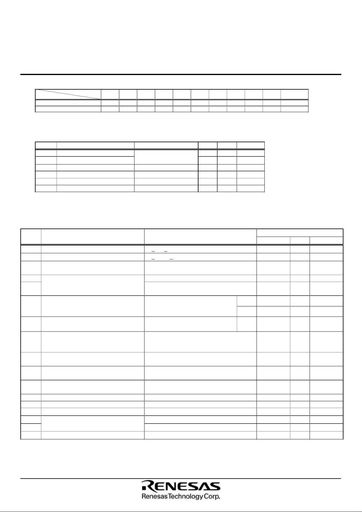
Symbol Parameter
tRC tAVAV Read Cycle Time 70 ns
ta(AD) tAVQV Address Access Time 70 ns
ta(CE) tELQV Chip Enable Access Time 70 ns
ta(OE) tGLQV Output Enable Access Time 30 ns
ta(PAD) tPAVQV Page Read Access Time 25 ns
tCEPH CE# "H"Pulse width 30 ns
tCLZ tELQX Chip Enable to Output in Low-Z 0 ns
tDF(CE) tEHQZ Chip Enable High to Output in High-Z 25 ns
tOLZ tGLQX Output Enable to Output in Low-Z 0 ns
tDF(OE) tGHQZ Output Enable to High to Output in High-Z 25 ns
tPHZ tPLQZ RP# Low to Output High-Z 150 ns
ta(BYTE) tFL/HQV BYTE# access time 70 ns
tBHZ tFLQZ BYTE# low to output high-Z 25 ns
tOH tOH Output Hold from CE#, OE# and Addresses 0 ns
tBCD tELFL/H CE# low to BYTE# high or low 5 ns
tBAD tAVFL/H Address to BYTE# high or low 5 ns
tOEH tWHGL OE# Hold from WE# High 10 ns
tPS tPHEL RP# Recovery to CE# Low 150 ns
Flash VCC=3.0-3.6V
Min. Typ. Max.
Units
-Timing measurements are made under AC waveforms for read operations.
15
Rev.0.2_48a_bezz
Page 16

Preliminary
Limits
Limits
Notice: This is not a final specification.
Some parametric limits are subject to change.
Renesas LSIs
M5M29KE131BVP
134,217,728-BIT (16,777,216-WORD BY 8-BIT / 8,388,608-WORD BY 16-BIT)
CMOS FLASH MEMORY
Stacked-uMCP (micro Multi Chip Package)
AC electrical characteristics
(Ta=-40 ~85 °C and Flash VCC=3.0V~3.6V, unless otherwise noted)
Read / Write Mode (WE# control)
Symbol Parameter
tWC tAVAV Write Cycle Time 70 ns
tAS tAVWH Address Setup Time 35 ns
tAH tWHAX Address Hold Time 0 ns
tDS tDVWH Data Setup Time 35 ns
tDH tWHDX Data Hold Time 0 ns
tOEH tWHGL OE# Hold from WE# High 10 ns
tCS tELWL Chip Enable Setup Time 0 ns
tCH tWHEH Chip Enable Hold Time 0 ns
tWP tWLWH Write Pulse Width 35 ns
tWPH tWHWL Write Pulse Width High 30 ns
tBS tFL/HWH Byte enable high or low set-up time 35 ns
tBH tWHFL/H Byte enable high or low hold time 70 ns
tGHWL tGHWL OE# Hold to WE# Low 0 ns
tBLS tPHHWH Block Lock Setup to Write Enable High 70 ns
tBLH tQVPH Block Lock Hold from Valid SRD 0 ns
tDAP tWHRH1 Duration of Auto Program Operation(Word Mode) 30 300 µs
tDAP tWHRH1 Duration of Auto Program Operation(Byte Mode) 30 300 µs
tDAP tWHRH1 Duration of Auto Program Operation(Page Mode) 4 80 ms
tDAE tWHRH2 Duration of Auto Block Erase Operation 150 600 ms
tWHRL tWHRL Delay Time During Internal Operation 70 ns
tPS tPHWL RP# Recovery to CE# Low 150 ns
-Read timing parameters during command write operations mode are the same as during read only operation mode.
-Typical values at Flash VCC=3.3V and Ta=25 °C.
Flash VCC=3.0-3.6V
Min. Typ. Max.
Units
Read / Write Mode (CE# control)
Symbol Parameter
tWC tAVAV Write Cycle Time 70 ns
tAS tAVEH Address Setup Time 35 ns
tAH tEHAX Address Hold Time 0 ns
tDS tDVEH Data Setup Time 35 ns
tDH tEHDX Data Hold Time 0 ns
tOEH tEHGL OE# Hold from CE# High 10 ns
tWS tWLEL Write Enable Setup Time 0 ns
tWH tEHWH Write Enable Hold Time 0 ns
tCEP tELEH CE# Pulse Width 35 ns
tCEPH tEHEL CE#"H" Pulse Width 30 ns
tBS tFL/HEH Byte enable high or low set-up time 35 ns
tBH tEHFL/H Byte enable high or low hold time 70 ns
tGHEL tGHEL OE# Hold to CE# Low 0 ns
tBLS tPHHEH Block Lock Setup to Write Enable High 70 ns
tBLH tQVPH Block Lock Hold from Valid SRD 0 ns
tDAP tEHRH1 Duration of Auto Program Operation(Word Mode) 30 300 µs
tDAP tEHRH1 Duration of Auto Program Operation(Byte Mode) 30 300 µs
tDAP tEHRH1 Duration of Auto Program Operation(Page Mode) 4 80 ms
tDAE tEHRH2 Duration of Auto Block Erase Operation 150 600 ms
tEHRL tEHRL Delay Time During Internal Operation 70 ns
tPS tPHEL RP# Recovery to CE# Low 150 ns
-Timing measurements are made under AC waveforms for read operations.
-Typical values at Flash VCC=3.3V and Ta=25 °C.
Flash VCC=3.0-3.6V
Min. Typ. Max.
Units
16
Rev.0.2_48a_bezz
Page 17

Preliminary
F-RP#=VIH Setup Time from Flash VCC min.
Notice: This is not a final specification.
Some parametric limits are subject to change.
134,217,728-BIT (16,777,216-WORD BY 8-BIT / 8,388,608-WORD BY 16-BIT)
Program / Erase Time
Parameter Min. Typ. Max. Units
Block Erase Time 150 600 ms
Main Block Write Time (Byte Mode) 2 8 sec
Main Block Write Time (Word Mode) 1 4 sec
Page Write Time 4 80 ms
Flash to Page Buffer Time 100 150 µs
Program Suspend / Erase Suspend Time
Parameter Min. Typ. Max. Unit
Program Susupend Time 15 µs
Erase Susupend Time 15 µs
Flash VCC Power Up / Down Timing
Renesas LSIs
M5M29KE131BVP
CMOS FLASH MEMORY
Stacked-uMCP (micro Multi Chip Package)
symbol Parameter Min. Typ. Max. Unit
tVCS
tVHEL F-CE#=VIL Setup Time from Flash VCC min. 60 µs
During power up / down, by the noise pulses on control pins, the device has possibility of accidental erase of programming.
The device must be protected against initiation of write cycle for memory contents during power up / down. The delay time
of min. 60 µsec is always required before read operation or write operation is initiated from the time Flash VCC reaches
Flash VCC min. during power up /down. By holding F-RP#=VIL, the contents of memory is protected during Flash VCC
power up / down. During power up, F-RP# must be held VIL for min. 2µs from the time Flash VCC reaches Flash VCC min..
During power down, F-RP# must be held VIL until Flash VCC reaches GND. F-RP# doesn’t have latch mode, therefore FRP# must be held VIH during read operation or erase / program operation.
2 µs
17
Rev.0.2_48a_bezz
Page 18

Preliminary
IH
IL
IH
IL
IHVIL
IHVIL
OHVOVIHVIL
Read /Write Inhibit
Read /Write Inhibit
Read /Write Inhibit
Notice: This is not a final specification.
Some parametric limits are subject to change.
Flash VCC Power up / down Timing
Renesas LSIs
M5M29KE131BVP
134,217,728-BIT (16,777,216-WORD BY 8-BIT / 8,388,608-WORD BY 16-BIT)
CMOS FLASH MEMORY
Stacked-uMCP (micro Multi Chip Package)
3.0V
V
CC
RP#
CE#
WE#
GND
V
IH
V
IL
V
IH
V
IL
V
IH
V
IL
t
VHEL
t
VCS
t
PS
t
PS
AC Waveforms for Read Operation and Test Conditions
t
RC
(WORD)
V
V
V
Address Valid
t
a(AD)
V
t
V
CEPH
t
OEH
t
a(CE)
V
t
a(OE)
t
CLZ
OLZ
Output Valid
V
High-Z
FFH
t
PS
t
A22-A
0
A22 -A-1 (BYTE)
F-CE#
OE#
WE#
DATA
F-RP#
t
DF(CE)
t
DF(OE)
t
OH
t
PHZ
High-Z
Test Conditions for
AC Characteristics
Input Voltage : VIL=0V, VIH=Flash Vcc
Input Rise and Fall Times : <5ns
Reference Voltage
at timing measurement : (Flash Vcc)/2
Output Load : 1 TTL gate +
CL(30pF)
or
1.3V
1N914
3.3kohm
DUT
CL=30pF
18
- After inputting Read Array Command FFH, it is necessary to make F-CE# “H” pulse more than 30ns (tCEPH).
And after inputting Read Array Command FFH, it is also necessary to keep 30ns to recover before starting read
after WE# rises “H” in case of changing a part or all of addresses( A22~A0/A22~A-1) and F-CE#= “L”.
Rev.0.2_48a_bezz
Page 19

Preliminary
D7-D0
IHVIL
IHVILVIHVIL
IHVIL
OHVOL
D14-D8
OHVOL
IHVIL
Notice: This is not a final specification.
Some parametric limits are subject to change.
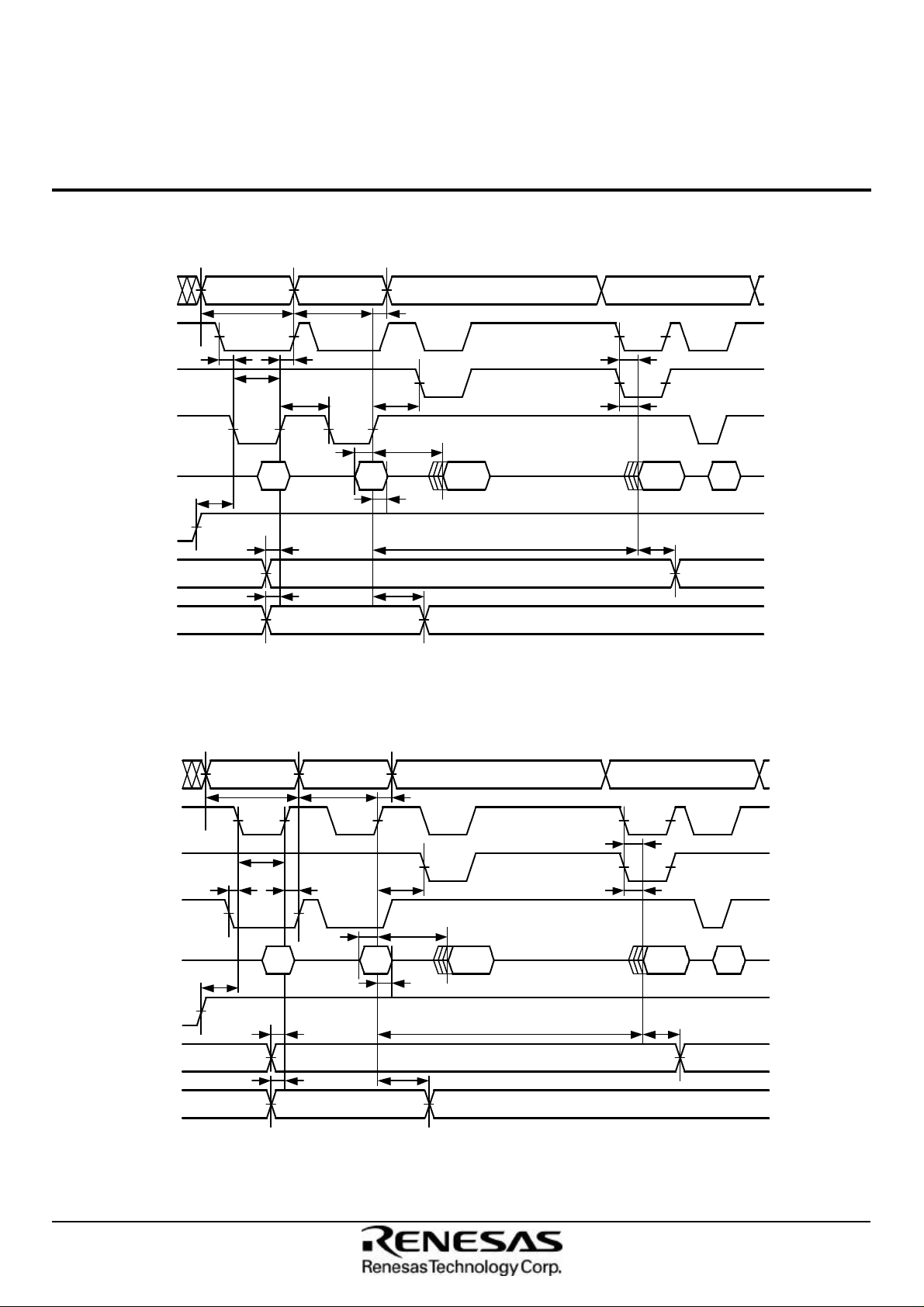
Byte AC Waveforms for Read Operation
Renesas LSIs
M5M29KE131BVP
134,217,728-BIT (16,777,216-WORD BY 8-BIT / 8,388,608-WORD BY 16-BIT)
CMOS FLASH MEMORY
Stacked-uMCP (micro Multi Chip Package)
ADDRESS
A22-A0
F-CE#
OE#
BYTE#
DATA
DATA
D15/A-1
V
Address Valid
t
t
BCD
t
BAD
t
CLZ
a(AD)
t
a(BYTE)
t
a(CE)
t
a(OE)
t
OLZ
t
BAD
Output Valid
V
V
V
High-Z
V
High-Z
V
Address Valid
When BYTE# = VIH, F-CE# = OE# = VIL, D15/A-1 is output status. At this time, input signal must not be applied.
Address Valid
t
a(BYTE)
t
BHZ
Valid Valid
Valid
t
a(AD)
D15 A-1
t
DF(CE)
t
DF(OE)
t
OH
19
Rev.0.2_48a_bezz
Page 20

Preliminary
Notice: This is not a final specification.
Some parametric limits are subject to change.
134,217,728-BIT (16,777,216-WORD BY 8-BIT / 8,388,608-WORD BY 16-BIT)
AC Waveforms for Word / Byte Program Operation (WE# Control)
V
(Word)
(Byte)
IH
Bank Address
High-Z
t
BLS
Valid
t
t
t
BS
WC
PS
t
WP
V
IL
V
IH
V
IL
t
CS
V
IH
V
IL
V
IH
V
IL
V
IH
V
IL
V
IH
V
IL
V
IH
V
IL
V
IH
V
IL
40H
t
WPH
Address Valid
t
AS
t
CH
t
DS
DIN
t
OEH
Bank Address Valid
t
AH
t
WHRL
SRD
DH
Busy
t
BH
t
Program
t
DAP
ADDRESS
A22-A
0
A22-A
-1
F-CE#
OE#
WE#
DATA
F-RP#
F-WP#
BYTE#
Renesas LSIs
M5M29KE131BVP
CMOS FLASH MEMORY
Stacked-uMCP (micro Multi Chip Package)
Bank Address Valid
Read Status Register
t
a(CE)
t
a(OE)
SRD
Ready
t
BLH
FFH
Write Read Array Command
AC Waveforms for Word / Byte Program Operation (F-CE# Control)
V
(Word)
(Byte)
IH
Bank Address
t
WS
High-Z
t
BLS
t
Valid
t
WC
t
PS
BS
t
CEP
V
IL
V
IH
V
IL
V
IH
V
IL
V
IH
V
IL
V
IH
V
IL
V
IH
V
IL
V
IH
V
IL
V
IH
V
IL
40H
Address Valid
t
AS
t
WH
t
DS
DIN
Bank Address Valid
t
t
OEH
t
EHRL
t
DH
AH
Program
SRD
Busy
t
BH
t
DAP
ADDRESS
A22-A
0
A22-A
-1
F-CE#
OE#
WE#
DATA
F-RP#
F-WP#
BYTE#
Bank Address Valid
Read Status Register
t
a(CE)
t
a(OE)
SRD
Ready
Write Read Array Command
t
BLH
FFH
20
Rev.0.2_48a_bezz
Page 21

Preliminary
\
Notice: This is not a final specification.
Some parametric limits are subject to change.
134,217,728-BIT (16,777,216-WORD BY 8-BIT / 8,388,608-WORD BY 16-BIT)
AC Waveforms for Page Program Operation (WE# Control)
V
IH
A22-A
7
(Word)
0
-1
(Byte)
V
V
A6-A
A6-A
V
V
F-CE#
V
V
OE#
V
V
WE#
V
V
DATA 41H DIN
V
V
F-RP#
V
V
F-WP#
V
V
BYTE#
V
IL
IH
IL
IH
IL
t
IH
IL
IH
IL
IH
IL
IH
IL
IH
IL
IH
IL
Bank Address
CS
High-Z
t
BLS
t
BS
Valid
t
WC
t
WPtWPH
t
PS
Address Valid
00H 01H-7EH 7FH
00H 01H-FEH FFH
t
AS
t
CH
AC Waveforms for Page Program Operation (F-CE# Control)
The Other Bank
Address Valid
Valid
Valid
t
AH
t
OEH
t
DH
t
DS
t
a(CE)
t
a(OE)
DOUT
Address Valid
t
GHWL
DIN DIN
Renesas LSIs
M5M29KE131BVP
CMOS FLASH MEMORY
Stacked-uMCP (micro Multi Chip Package)
Bank Address Valid
t
OEH
t
WHRL
SRD
t
BH
Bank Address Valid
Read Status Register
Busy
t
a(CE)
t
a(OE)
SRD
Ready
Write Read Array Command
t
DAP
t
BLH
FFH
V
IH
A22 - A
7
(Word)
(Byte)
-1
V
V
V
A6-A
A6-A
0
V
F-CE#
V
V
OE#
V
V
WE#
V
V
DATA 41H DIN
V
V
F-RP#
V
V
F-WP#
V
V
BYTE#
V
IL
IH
IL
IH
IL
IH
IL
IH
IL
IH
IL
IH
IL
IH
IL
IH
IL
t
WS
High-Z
Bank Address
Valid
t
WC
t
CEP
t
PS
t
BLS
t
BS
Address Valid
00H 01H-7EH 7FH
00H 01H-FEH FFH
t
AS
t
WH
t
CEPH
The Other Bank
Address Valid
Valid
Valid
t
AH
t
OEH
t
DH
t
DS
t
a(CE)
t
a(OE)
DOUT
Address Valid
t
GHEL
DIN DIN
Bank Address Valid
t
OEH
t
EHRL
SRD
Busy
t
BH
Bank Address Valid
Read Status Register
SRD
Ready
t
DAP
t
BLH
t
a(CE)
t
a(OE)
FFH
Write Read Array Command
21
Rev.0.2_48a_bezz
Page 22
Preliminary
Notice: This is not a final specification.
Some parametric limits are subject to change.
134,217,728-BIT (16,777,216-WORD BY 8-BIT / 8,388,608-WORD BY 16-BIT)
AC Waveforms for Erase Operation (WE# Control)
V
(Word)
(Byte)
IH
Bank Address
High-Z
t
BLS
t
Valid
t
WC
t
PS
BS
t
WP
V
IL
V
IH
V
IL
t
CS
V
IH
V
IL
V
IH
V
IL
V
IH
V
IL
V
IH
V
IL
V
IH
V
IL
V
IH
V
IL
Address Valid
t
AS
t
CH
t
WPH
t
DS
D0H
Bank Address Valid
t
AH
t
OEH
t
WHRL
t
DH
t
ADDRESS
A22-A
0
A22-A
-1
F-CE#
OE#
WE#
DATA 20H
F-RP#
F-WP#
BYTE#
BH
SRD
Busy
Erase
t
DAE
Renesas LSIs
M5M29KE131BVP
CMOS FLASH MEMORY
Stacked-uMCP (micro Multi Chip Package)
Bank Address Valid
Read Status Register
t
a(CE)
t
a(OE)
SRD
Ready
t
BLH
FFH
Write Read Array Command
AC Waveforms for Erase Operation (F-CE# Control)
V
(Word)
(Byte)
IH
Bank Address
t
WS
High-Z
t
BLS
t
Valid
t
WC
t
t
PS
BS
CEP
V
IL
V
IH
V
IL
V
IH
V
IL
V
IH
V
IL
V
IH
V
IL
V
IH
V
IL
V
IH
V
IL
V
IH
V
IL
20H
Address Valid
t
AS
t
WH
t
DS
D0H
Bank Address Valid
t
AH
t
OEH
t
EHRL
SRD
t
DH
t
BH
Erase
Busy
ADDRESS
A22-A
0
A22-A
-1
F-CE#
OE#
WE#
DATA
F-RP#
F-WP#
BYTE#
t
DAE
Bank Address Valid
Read Status Register
t
a(CE)
t
a(OE)
SRD
Ready
Write Read Array Command
t
BLH
FFH
22
Rev.0.2_48a_bezz
Page 23

Preliminary
Notice: This is not a final specification.
Some parametric limits are subject to change.
134,217,728-BIT (16,777,216-WORD BY 8-BIT / 8,388,608-WORD BY 16-BIT)
AC Waveforms for Word / Byte Program Operation with BGO (WE# Control)
M5M29KE131BVP
Stacked-uMCP (micro Multi Chip Package)
Renesas LSIs
CMOS FLASH MEMORY
Change Bank Address
Address
Valid
Address
Valid
t
a(CE)
t
a(OE)
DOUT DOUT
WP
Program in one bank
Address Valid
t
AS
t
CH
t
WPH
t
DS
V
(Byte)
IH
Bank Address
High-Z
Valid
t
WC
t
V
7
IL
V
IH
V
IL
V
IH
V
IL
t
CS
V
IH
V
IL
V
IH
V
IL
V
IH
V
IL
ADDRESS
A22 - A
A6-A
(Word)
0
A6-A
-1
F-CE#
OE#
WE#
DATA 40H DIN
Read Status Register Read Array in another bank
Address Valid
t
AH
t
OEH
t
WHRL
SRD
t
DH
Program
Busy
AC Waveforms for Word / Byte Program Operation with BGO (F-CE# Control)
Address
Valid
Address
Valid
CEP
Program in one bank
Address Valid
t
AS
t
WH
t
DS
V
(Byte)
IH
Bank Address
t
WS
High-Z
Valid
t
WC
t
V
IL
7
V
IH
V
IL
V
IH
V
IL
V
IH
V
IL
V
IH
V
IL
V
IH
V
IL
ADDRESS
A22 - A
A6-A
(Word)
0
A6-A
-1
F-CE#
OE#
WE#
DATA 40H DIN
Read Status Register Read Array in another bank
Address Valid
t
AH
t
OEH
t
EHRL
SRD
t
DH
Program
Busy
Change Bank Address
Address
Valid
Address
Valid
Address
Valid
Address
Valid
t
a(CE)
t
a(OE)
DOUT DOUT
23
Rev.0.2_48a_bezz
Page 24

Preliminary
\
Change Bank Address
Notice: This is not a final specification.
Some parametric limits are subject to change.
134,217,728-BIT (16,777,216-WORD BY 8-BIT / 8,388,608-WORD BY 16-BIT)
AC Waveforms for Page Program Operation with BGO (WE# Control)
M5M29KE131BVP
Stacked-uMCP (micro Multi Chip Package)
Renesas LSIs
CMOS FLASH MEMORY
V
IH
A22-A
7
V
A6-A
(Word)
0
V
A6-A
(Byte)
-1
V
V
F-CE#
V
V
OE#
V
V
WE#
V
V
DATA 41H DIN
V
IL
IH
IL
IH
IL
t
IH
IL
IH
IL
IH
IL
Bank Address
CS
High-Z
Valid
t
WC
t
WPtWPH
00H 01H-7EH 7FH
00H 01H-FEH FFH
t
AS
t
CH
Program in one bank
Address Valid
t
AH
t
DH
t
DS
DIN DIN
t
OEH
t
WHRL
SRD
Busy
AC Waveforms for Page Program Operation with BGO (F-CE# Control)
t
OEH
t
EHRL
Change Bank Address
SRD
Busy
7
(Word)
(Byte)
-1
V
IH
Bank Address
V
IL
V
IH
V
IL
V
IH
V
IL
t
WS
V
IH
V
IL
V
IH
V
IL
V
IH
High-Z
V
IL
Valid
t
WC
t
CEPtCEPH
00H 01H-7EH 7FH
00H 01H-FEH FFH
t
AS
t
WH
ADDRESS
A22 - A
A6-A
0
A6-A
F-CE#
OE#
WE#
DATA 41H DIN
Program in one bank
Address Valid
t
AH
t
DH
t
DS
DIN DIN
Read Array in another bank
Address
Valid
Address
Valid
DOUT DOUT
Read Array in another bank
Address
Valid
DOUT DOUT
t
DAP
t
a(CE)
t
a(OE)
t
t
Address
Valid
Address
Valid
Address
Valid
a(CE)
a(OE)
24
Rev.0.2_48a_bezz
Page 25

Preliminary
Notice: This is not a final specification.
Some parametric limits are subject to change.
134,217,728-BIT (16,777,216-WORD BY 8-BIT / 8,388,608-WORD BY 16-BIT)
AC Waveforms for Erase Operation with BGO (WE# Control)
Renesas LSIs
M5M29KE131BVP
CMOS FLASH MEMORY
Stacked-uMCP (micro Multi Chip Package)
Change Bank Address
ADDRESS
A22-A
(Word)
0
A22-A
(Byte)
-1
F-CE#
OE#
WE#
DATA
V
IH
Bank Address
V
IL
V
IH
V
IL
t
CS
V
IH
V
IL
V
IH
V
IL
V
IH
High-Z
V
IL
Valid
t
WC
t
WP
20H
t
WPH
t
AS
t
CH
t
DS
D0H
Read Status Register Read Array in another bankProgram in one bank
Address Valid
t
OEH
t
WHRL
t
DH
SRD
Busy
AC Waveforms for Erase Operation with BGO (F-CE# Control)
Address
Valid
t
AH
t
a(CE)
t
a(OE)
DOUT DOUT
Address
Valid
ADDRESS
A22-A
(Word)
0
A22-A
(Byte)
-1
F-CE#
OE#
WE#
DATA
Change Bank Address
V
IH
Bank Address
WS
Valid
t
WC
t
CEP
20H
t
t
WH
DS
t
AS
V
IL
V
IH
V
IL
V
IH
V
IL
t
V
IH
V
IL
V
IH
High-Z
V
IL
Address Valid
t
OEH
D0H
t
EHRL
SRD
t
DH
Busy
Read Array in another bankRead Status RegisterProgram in one bank
Address
Valid
t
AH
t
a(CE)
t
a(OE)
Address
Valid
DOUTDOUT
25
Rev.0.2_48a_bezz
Page 26

Preliminary
IHVIL
IH
IL
IHVIL
IHVIL
IH
IL
IHVIL
IHVIL
CStCHtWP
AHtAS
OEH
BLHta(OE)ta(CE)
ADDRESS
Notice: This is not a final specification.
Some parametric limits are subject to change.
134,217,728-BIT (16,777,216-WORD BY 8-BIT / 8,388,608-WORD BY 16-BIT)
AC Waveforms for Suspend Operation (WE# Control)
Renesas LSIs
M5M29KE131BVP
CMOS FLASH MEMORY
Stacked-uMCP (micro Multi Chip Package)
(Word)
0
-1
(Byte)
V
Bank Address Valid
V
V
t
ADDRESS
A22-A
A22-A
F-CE#
V
OE#
V
WE#
V
DATA B0H
High-Z
V
V
F-RP#
V
F-WP#
t
t
Suspend Time
Bank Address Valid
Read Status Register
S.R.6,7=1
SRD
Valid
t
AC Waveforms for Suspend Operation (F-CE# Control)
V
(Word)
(Byte)
-1
IH
V
IL
V
IH
V
IL
V
IH
V
IL
V
IH
V
IL
V
IH
High-Z
V
IL
V
IH
V
IL
V
IH
V
IL
A22-A
0
A22-A
F-CE#
OE#
WE#
DATA B0H
F-RP#
F-WP#
Bank Address Valid
t
AS
t
t
WS
CEP
t
WH
t
AH
t
OEH
Suspend Time
Bank Address Valid
Read Status Register
t
a(CE)
t
a(OE)
S.R.6,7=1
SRD
Valid
t
BLH
26
Rev.0.2_48a_bezz
Page 27

Preliminary
IH
IL
IH
IL
IH
IL
IH
IL
IH
IL
CStWPtWCta(OE)
a(CE)
CHta(AD)ta(OE)
a(AD)ta(OE)
a(AD)
a(CE)ta(CE)
IHVIL
IHVIL
IH
IL
IHVIL
IH
IL
CStWP
Bank Address Valid
Address Valid
CH
a(AD)
a(AD)
Notice: This is not a final specification.
Some parametric limits are subject to change.
134,217,728-BIT (16,777,216-WORD BY 8-BIT / 8,388,608-WORD BY 16-BIT)
AC Waveforms for Device ID Read Operation with BBR(Back Bank Read)
M5M29KE131BVP
Stacked-uMCP (micro Multi Chip Package)
Renesas LSIs
CMOS FLASH MEMORY
ADDRESS
A22 - A
V
V
0
Bank Address Valid Address ValidAddress Valid Bank Address Valid
V
F-CE#
V
t
V
OE#
V
V
WE#
DATA 90H
V
V
High-Z
V
Change Bank Address
t
Return Bank Address
t
t
t
ID
ID
t
Dout
AC Waveforms for Status Register Read Operation with BBR(Back Bank Read)
ADDRESS
A22 - A
V
0
V
F-CE#
t
V
OE#
V
V
WE#
V
DATA 70H
High-Z
V
Change Bank Address
t
a(CE)
t
t
EHRL
t
a(OE)
t
a(OE)
t
SRD
Return Bank Address
t
a(CE)
Bank Address Valid
t
Dout
t
a(CE)
t
SRD
a(OE)
27
Rev.0.2_48a_bezz
Page 28

Preliminary
Notice: This is not a final specification.
Some parametric limits are subject to change.
Renesas LSIs
M5M29KE131BVP
134,217,728-BIT (16,777,216-WORD BY 8-BIT / 8,388,608-WORD BY 16-BIT)
CMOS FLASH MEMORY
Stacked-uMCP (micro Multi Chip Package)
Word / Byte Program Flow Chart
Start
Write 40H
Write Address,
Data
Status Register
Read
SR.7 = 1?
YES
Full Status Check
If Desired
Word / Byte Program
Completed
NO
Write
B0H?
YES
Suspend Loop
Write D0H
NO
YES
Block Erase Flow Chart
Start
Page Program Flow Chart
Start
Write 41H
n = 0
Write Address n,
DATA n
n = 7FH?
n = FFH?
YES
Status Register
Read
SR.7 = 1?
YES
Full Status Check
If Desired
Page Program
Completed
NO
NO
Suspend Loop
n = n + 1
Write
B0H?
YES
Write D0H
YES
NO
Write 20H
Write D0H
Block Address
Status Register
Read
SR.7 = 1?
YES
Full Status Check
If Desired
Erase
Completed
28
NO
Write
B0H?
YES
Suspend Loop
Write D0H
YES
NO
Status Register Check Flow Chart
Start
SR.4,5 = 1?
NO
SR.5 = 0?
YES
SR.4 = 0?
YES
SR.3 = 0?
YES
Pass
(Block Erase, Program)
YES
NO
NO
NO
Command
Sequence Error
Block Erase
Error
Program Error
(Page Program)
Block Erase Error
(Block Fail)
Rev.0.2_48a_bezz
Page 29

Preliminary
Notice: This is not a final specification.
Some parametric limits are subject to change.
Renesas LSIs
M5M29KE131BVP
134,217,728-BIT (16,777,216-WORD BY 8-BIT / 8,388,608-WORD BY 16-BIT)
CMOS FLASH MEMORY
Stacked-uMCP (micro Multi Chip Package)
Single Data Load to Page Buffer
Flow Chart
Start
Write 74H
Write Address,
Data
Load
Finished?
Single Data Load
To Page Buffer
Completed
NO
YES
Page Buffer to Flash Flow Chart
Start
Suspend / Resume Flow Chart
Start
NO
NO
Suspend
Erase/ Program
Finished
Write B0H
Status Register
Read
S.R. 7=1?
YES
S.R. 6=1?
YES
Write FFH
Read Array
Data
Write 0EH
Write D0H
Page Address
Status Register
Read
SR.7 = 1?
YES
Full Status Check
If Desired
Page Buffer
To Flash
Completed
NO
Write
BOH?
YES
Suspend Loop
Write D0H
YES
NO
Read
Finished?
Write D0H
Operation
Restart
NO
YES
Clear Page Buffer Flow Chart
Start
Write 55H
Write D0H
Clear Page Buffer
Completed
Resume
29
Rev.0.2_48a_bezz
Page 30

Preliminary
Bank Address
Bank Address
(Random Read)
(Random Read)
Notice: This is not a final specification.
Some parametric limits are subject to change.
Operation Status (F-WP#=VIH)
Renesas LSIs
M5M29KE131BVP
134,217,728-BIT (16,777,216-WORD BY 8-BIT / 8,388,608-WORD BY 16-BIT)
CMOS FLASH MEMORY
Stacked-uMCP (micro Multi Chip Package)
Back Bank Read State
Read Array
(Random Read)
Setup State
Clear Page Buffer
Setup
55H
Ready
Clear
Status Register
Single Data Load
to Page Buffer
Setup
Change Bank
Address
Others
74H
Page Buffer
50H
3)
D0H
Flash to
Setup
Read/Standby State
(Random Read Mode)
WD
D0H
F1H
0EH
Page Buffer to
Flash
Setup
Other
D0H
Status Register
Device Identifier
41H 40H
Page Program
Setup
Wdi
I=0-127
Program &
Verify
Read
Read
Status Register
70H
90H
Read
90H
WD
70H
FFH
Read Array
(Random Read)
FFH
Word Program
Setup
Internal State
B0H B0H
D0H D0H
Block Erase
Setup
D0H
Erase &
Verify
Read
Status Register
20H
D0H
A7H
Erase All Unlocked
Blocks Setup
Others
Change
Read State with BGO
Read Array
Suspend
Read
Status Register
70H
State
Read State with BGO
Read Array
Change
FFH
Read Array
(Random Read)
1) After setting up Clear Page Buffer, D0H enables to clear Page Buffer.
2) To access any bank during Erase All Unlocked Block results Status Register Read.
Although Read Status Register Command and Read Array Command can be issued under Suspend State,
output data make no sense.
30
Rev.0.2_48a_bezz
Page 31

Preliminary
Release Setup
Release Setup
Release Setup
Release Setup
Release Setup
Others
3)
7BH
Others
Others
Others
Notice: This is not a final specification.
Some parametric limits are subject to change.
Operation Status (F-WP#=VIL)
Renesas LSIs
M5M29KE131BVP
134,217,728-BIT (16,777,216-WORD BY 8-BIT / 8,388,608-WORD BY 16-BIT)
CMOS FLASH MEMORY
Stacked-uMCP (micro Multi Chip Package)
Back Bank Read State
Read Array
(Random Read)
Read Array
(Random Read)
Setup State
Clear Page Buffer
Setup
Clear
Status Register
Change Bank
Address
55H
Single Data Load
to Page Buffer
Setup
Change Bank
Address
D0H
4)
Others
WD
74H
Page Buffer
50H
Flash to
Setup
Read/Standby State
(Random Read Mode)
D0H
Software Lock
F1H
Page Buffer to
0EH
Flash
Setup
Device Identifier
BA#
Software Lock
Software Lock
Page Program
Setup
70H
90H
Read
90H
FFH
41H 40H
Word Program
Setup
Read
Status Register
70H
FFH
Read Array
(Random Read)
ACH
Software Lock
BA
20H
3)
Block Erase
Software Lock
Setup
60H
Wdi
Ready
Change Bank
Address
Read State with BGO
Other
Read Array
(Random Read)
D0H
I=0-127
Program &
Verify
Read
Status Register
WD
B0H B0H
D0H D0H
Status Register
Suspend
Internal State
Read
70H
State
Read State with BGO
Read Array
(Random Read)
Change Bank
Address Read Array
FFH
(Random Read)
1) BA, BA#: Block Address, Block Address# (Shown in Command List(F-WP#=VIL) in detail).
2) After setting up Clear Page Buffer, D0H enables to clear Page Buffer.
D0H
Erase &
Verify
Read
Status Register
Other
31
Rev.0.2_48a_bezz
Page 32

Preliminary
Notice: This is not a final specification.
Some parametric limits are subject to change.
Renesas LSIs
M5M29KE131BVP
134,217,728-BIT (16,777,216-WORD BY 8-BIT / 8,388,608-WORD BY 16-BIT)
CMOS FLASH MEMORY
Stacked-uMCP (micro Multi Chip Package)
Package Dimension
48P3R-C
32
Rev.0.2_48a_bezz
Page 33

Preliminary
Notice: This is not a final specification.
Some parametric limits are subject to change.
Renesas LSIs
M5M29KE131BVP
134,217,728-BIT (16,777,216-WORD BY 8-BIT / 8,388,608-WORD BY 16-BIT)
CMOS FLASH MEMORY
Stacked-uMCP (micro Multi Chip Package)
Nippon Bldg.,6-2,Otemachi 2-chome,Chiyoda-ku,Tokyo,100-0004 Japan
Keep safety first in your circuit designs!
• RenesasTechnology Corporation puts the maximum effort into making semiconductor products better and more reliable, but there is always the possibility that trouble may occur with them. Trouble with semiconductors may lead to
personal injury, fire or property damage.Remember to give due consideration to safety when making your circuit designs, with appropriate measures such as (i) placement of substitutive, auxiliary circuits, (ii) use of nonflammable
material or (iii) prevention against any malfunction or mishap.
Notes regarding these materials
• These materials are intended as a reference to assist our custom ers in the selection of theRenesas Technology Corporation product best suited to the customer's application; they do not convey any license under any intellectual
property rights, or any other rights, belonging to Renesas Technology Corporation or a third party.
• RenesasTechnology Corporation assumes no responsibility for any damage, or infringement of any third-party's rights, originating in the use of any product data, diagrams, charts, programs, algorithms, or circuit application
examples contained in these materials.
• All information contained in these materials, including product data, diagrams, charts, programs and algorithms represents information on products at the time of publication of these materials, and are subject to change by
Renesas Technology Corporation without notice due to product improvements or other reasons. It is therefore recommended that customers contact Renesas Technology Corporation or an authorized Renesas Technology
Corporation product distributor for the latest product information before purchasing a product listed herein.
The information described here may contain technical inaccuracies or typographical errors.
Renesas Technology Corporation assumes no responsibility for any damage, liability, or other loss rising from these inaccuracies or errors.
Please also pay attention to information published by Renesas Technology Corporation by various means, including the Renesas Technology Corporation Semiconductor home page (http://www.renesas.com).
• When using any or all of the information contained in these materials, including product data, diagrams, charts, programs, and algorithms, please be sure to evaluate all information as a total system before making a final decision
on the applicability of the information and products. Renesas Technology Corporation assumes no responsibility for any damage, liability or other loss resulting from the information contained herein.
• RenesasTechnology Corporation semiconductors are not designed or manufactured for use in a device or system that is used under circumstances in which human life is potentially at stake. Please contactRenesas Technology
Corporation or an authorized Renesas Technology Corporation product distributor when considering the use of a product contained herein for any specific purposes, such as apparatus or systems for transportation, vehicular,
medical, aerospace, nuclear, or undersea repeater use.
• The prior written approval ofRenesas Technology Corporation is necessary to reprint or reproduce in whole or in part these materials.
• If these products or technologies are subject to the Japanese export control restrictions, they must be exported under a license from the Japanese government and cannot be imported into a country other than the approved
destination.
• Any diversion or reexport contrary to the export control laws and regulations of Japan and/or the country of destination is prohibited.
• Please contactRenesas Technology Corporation for further details on these materials or the products contained therein.
REJ03C0183-0010Z
© 2003 Renesas Technology Corp.
New publication, effective April 2003.
Specifications subject to change without notice
 Loading...