

Page 1

REJ09B0110-0120
R8C/12 Group
16
Hardware Manual
RENESAS 16-BIT SINGLE-CHIP MICROCOMPUTER
M16C FAMILY / R8C /Tiny SERIES
All information contained in these materials, including products and product specifications,
represents information on the product at the time of publication and is subject to change by
Renesas Technology Corp. without notice. Please review the latest information published
by Renesas Technology Corp. through various means, including the Renesas Technology
Corp. website (http://www.renesas.com).
Rev. 1.20
Revision date: Jan 27, 2006
www.renesas.com
Page 2

Keep safety first in your circuit designs!
1.
Renesas Technology Corp. puts the maximum effort into making semiconductor products
better and more reliable, but there is always the possibility that trouble may occur with
them. Trouble with semiconductors may lead to personal injury, fire or property damage.
Remember to give due consideration to safety when making your circuit designs, with appropriate measures such as (i) placement of substitutive, auxiliary circuits, (ii) use of nonflammable material or (iii) prevention against any malfunction or mishap.
Notes regarding these materials
1.
These materials are intended as a reference to assist our customers in the selection of the
Renesas Technology Corp. product best suited to the customer's application; they do not
convey any license under any intellectual property rights, or any other rights, belonging to
Renesas Technology Corp. or a third party.
2.
Renesas Technology Corp. assumes no responsibility for any damage, or infringement of
any third-party's rights, originating in the use of any product data, diagrams, charts, programs, algorithms, or circuit application examples contained in these materials.
3.
All information contained in these materials, including product data, diagrams, charts, programs and algorithms represents information on products at the time of publication of these
materials, and are subject to change by Renesas Technology Corp. without notice due to
product improvements or other reasons. It is therefore recommended that customers contact Renesas Technology Corp. or an authorized Renesas Technology Corp. product distributor for the latest product information before purchasing a product listed herein.
The information described here may contain technical inaccuracies or typographical errors.
Renesas Technology Corp. assumes no responsibility for any damage, liability, or other
loss rising from these inaccuracies or errors.
Please also pay attention to information published by Renesas Technology Corp. by various means, including the Renesas Technology Corp. Semiconductor home page (http://
www.renesas.com).
4.
When using any or all of the information contained in these materials, including product
data, diagrams, charts, programs, and algorithms, please be sure to evaluate all information as a total system before making a final decision on the applicability of the information
and products. Renesas Technology Corp. assumes no responsibility for any damage, liability or other loss resulting from the information contained herein.
5.
Renesas Technology Corp. semiconductors are not designed or manufactured for use in a
device or system that is used under circumstances in which human life is potentially at
stake. Please contact Renesas Technology Corp. or an authorized Renesas Technology
Corp. product distributor when considering the use of a product contained herein for any
specific purposes, such as apparatus or systems for transportation, vehicular, medical,
aerospace, nuclear, or undersea repeater use.
6.
The prior written approval of Renesas Technology Corp. is necessary to reprint or reproduce in whole or in part these materials.
7.
If these products or technologies are subject to the Japanese export control restrictions,
they must be exported under a license from the Japanese government and cannot be imported into a country other than the approved destination.
Any diversion or reexport contrary to the export control laws and regulations of Japan and/
or the country of destination is prohibited.
8.
Please contact Renesas Technology Corp. for further details on these materials or the
products contained therein.
Page 3
How to Use This Manual
0
1. Introduction
This hardware manual provides detailed information on the R8C/12 Group of microcomputers.
Users are expected to have basic knowledge of electric circuits, logical circuits and microcomputers.
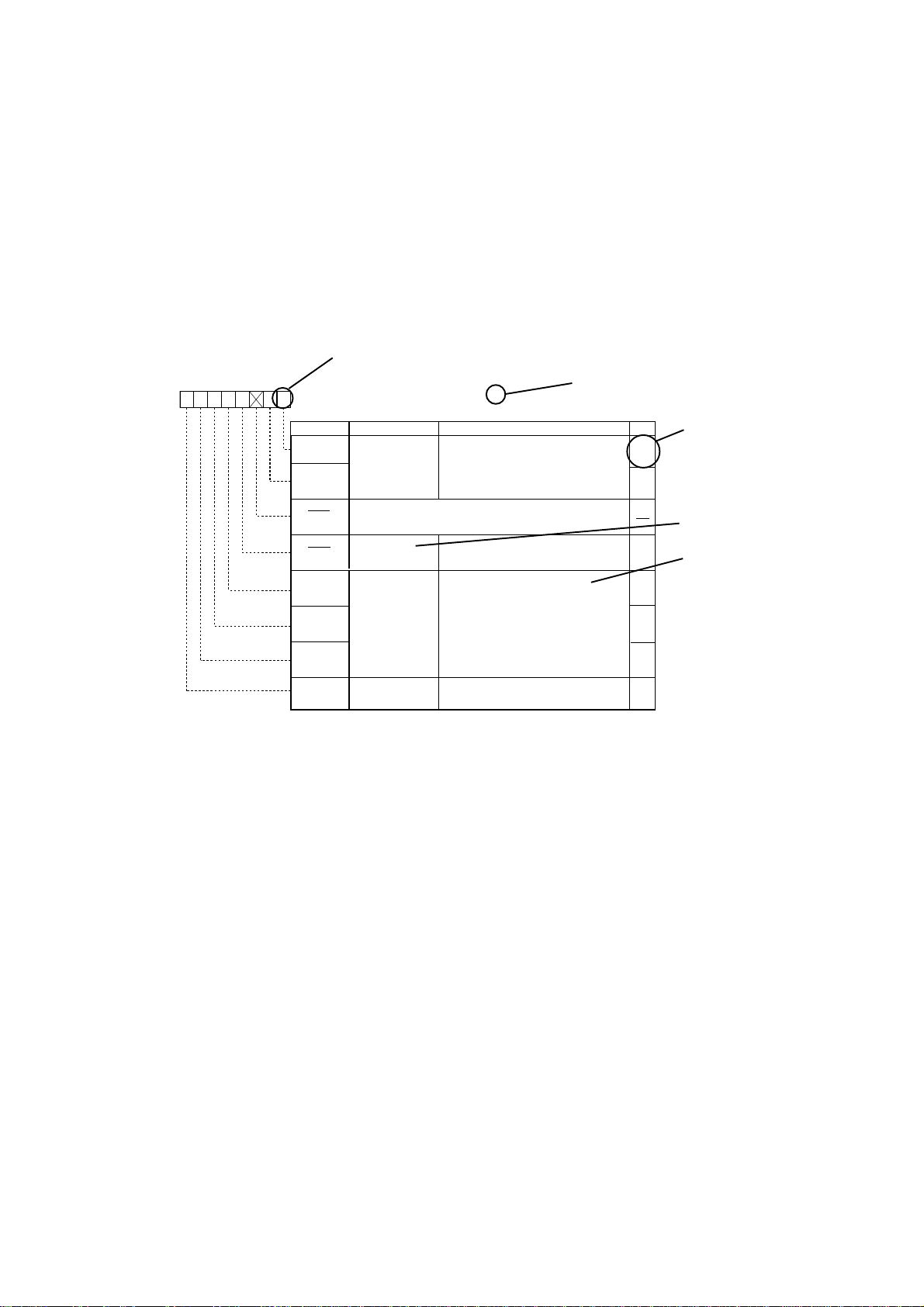
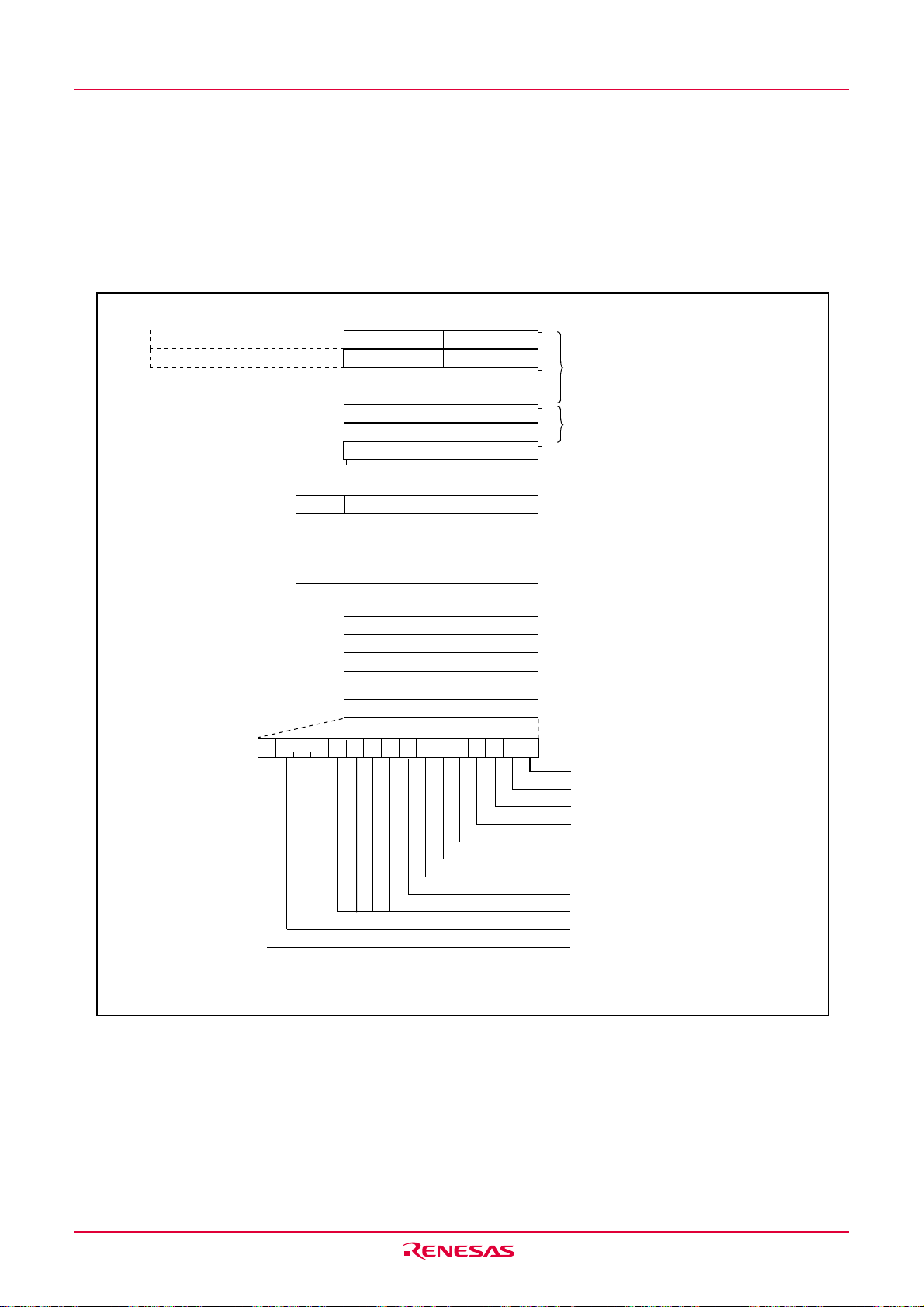
2. Register Diagram
The symbols, and descriptions, used for bit function in each register are shown below.
X X X r e g i s t e r
b 7b 6b 5b 4b 3b2b 1b 0
0
d d r e s
f t e r r e s e
X
S y m b o lA
X X XX
X X X
XXX1
(b2)
( b 3 )
XXX4
XXX5
X X X 6
X X X 7
Bit NameBit symbol
X X X B i t
N o t h i n g i s a s s i g n e d .
W h e n w r i t e , s h o u l d s e t t o " 0 " . W h e n r e a d , i t s c o n t e n t i s i n d e t e r m i n a t e .
R e s e r v e d B i t
X X X B i t
XXX Bit
sA
X0
b 1 b 0
1 0 : X X X
0 1 : X X X
1 0 : A v o i d t h i s s e t t i n g
1 1 : X X X
Must set to “0”
Function varies depending on each
operation mode
0: XXX
1: XXX
0
h
t
Function
*5
*1
Blank:Set to “0” or “1” according to the application
0: Set to “0”
1: Set to “1”
X: Nothing is assigned
*2
RW: Read and write
RO: Read only
WO: Write only
−: Nothing is assigned
*3
•Reserved bit
Reserved bit. Set to specified value.
*4
•Nothing is assigned
Nothing is assigned to the bit concerned. As the bit may be use for future functions,
set to “0” when writing to this bit.
•Do not set to this value
The operation is not guaranteed when a value is set.
•Function varies depending on mode of operation
Bit function varies depending on peripheral function mode.
Refer to respective register for each mode.
*5
Follow the text in each manual for binary and hexadecimal notations.
*1
RW
RW
RW
RW
R W
W O
R W
RO
*2
*3
*4
Page 4

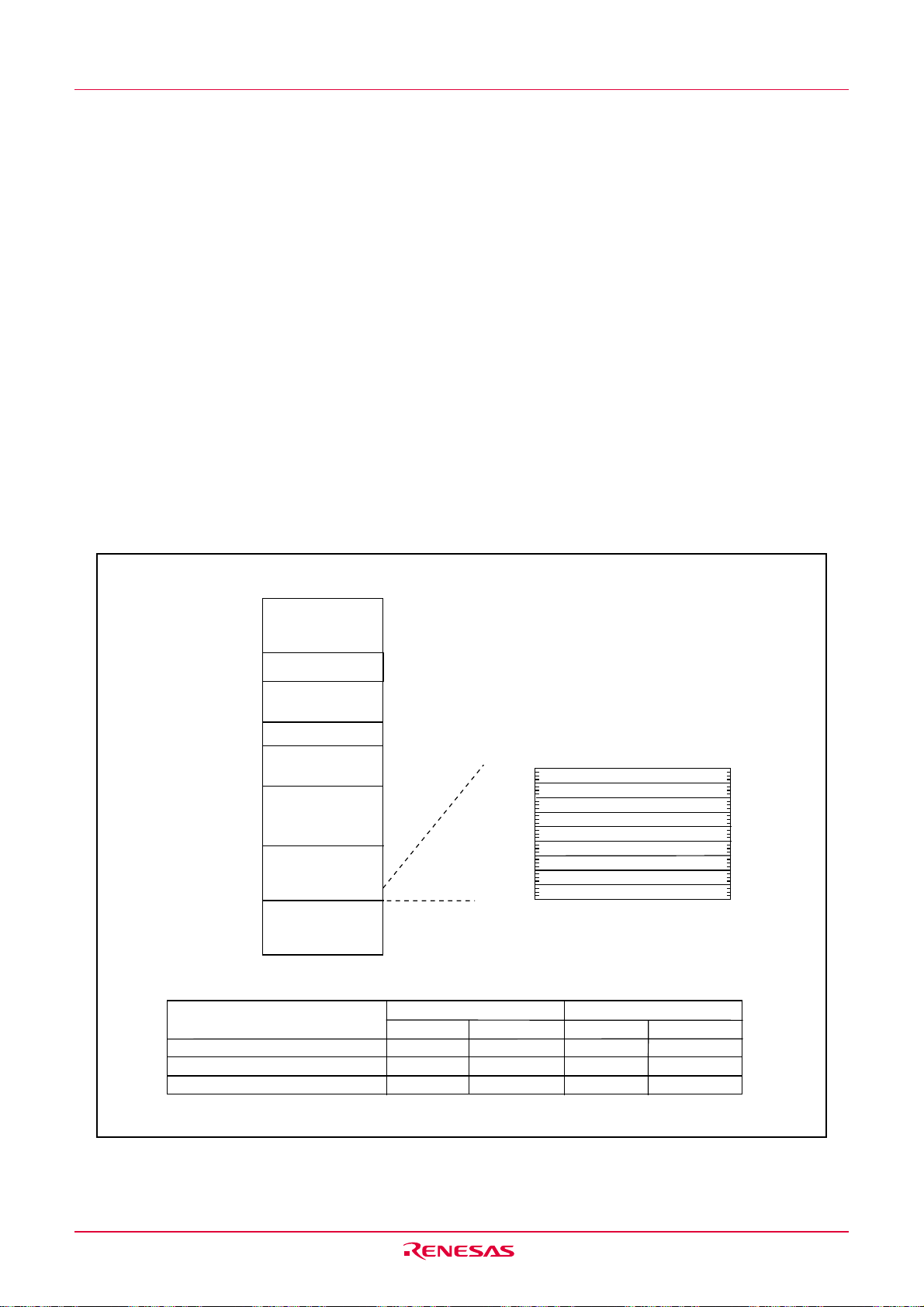
3. M16C Family Documents
The following documents were prepared for the M16C family.
(1)
Document
Short Sheet
Data Sheet
Hardware Manual
Software Manual
Application Note
RENESAS TECHNICAL UPDATE
NOTES:
1. Before using this material, please visit the our website to verify that this is the most updated
document available.
Hardware overview
Hardware overview and electrical characteristics
Hardware specifications (pin assignments, memory maps, peripheral
specifications, electrical characteristics, timing charts).
*Refer to the application note for how to use peripheral functions.
Detailed description of assembly instructions and microcomputer
performance of each instruction
• Usage and application examples of peripheral functions
• Sample programs
• Introduction to the basic functions in the M16C family
• Programming method with Assembly and C languages
Preliminary report about the specification of a product, a document,
etc.
Contents
Page 5

Table of Contents
SFR Page Reference
Chapter 1. Overview............................................................. 1
1.1 Applications ...................................................................................................................1
1.2 Performance Overview..................................................................................................2
1.3 Block Diagram ............................................................................................................... 3
1.4 Product Information ...................................................................................................... 4
1.5 Pin Assignments............................................................................................................5
1.6 Pin Description ..............................................................................................................6
Chapter 2. Central Processing Unit (CPU)......................... 7
2.1 Data Registers (R0, R1, R2 and R3 ) .............................................................................7
2.2 AddressRegisters (A0 and A1) ......................................................................................8
2.3 Frame Base Register( FB ).............................................................................................8
2.4 Interrupt Table Register (INTB ).....................................................................................8
2.5 Program Counter (PC )...................................................................................................8
2.6 User Stack Pointer (USP ) and Interrupt Stack Pointer (ISP )..................................... 8
2.7 Static Base Register (SB ) ............................................................................................. 8
2.8 Flag Register (FLG ) ....................................................................................................... 8
2.8.1 Carry Flag ( C Flag )................................................................................................................................8
2.8.2 Debug Flag ( D Flag ) ..............................................................................................................................8
2.8.3 Zero Flag ( Z Flag )..................................................................................................................................8
2.8.4 Sign Flag ( S Flag ).................................................................................................................................. 8
2.8.5 Register Bank Select Flag ( B Flag ) .....................................................................................................8
2.8.6 Overflow Flag ( O Flag)........................................................................................................................... 8
2.8.7 Interrupt Enable Flag ( I Flag ) ...............................................................................................................8
2.8.8 Stack Pointer Select Flag ( U Flag )....................................................................................................... 8
2.8.9 Processor Interrupt Priority Level ( IPL ) ..............................................................................................8
2.8.10 Reserved Area.......................................................................................................................................8
Chapter 3. Memory............................................................... 9
Chapter 4. Special Function Registers (SFR).................. 10
Chapter 5. Reset.................................................................. 14
5.1 Hardware Reset ............................................................................................................14
5.2 Software Reset..............................................................................................................14
5.3 Watchdog Timer Reset................................................................................................. 14
Chapter 6. Clock Generation Circuit.................................. 17
6.1 Main Clock.....................................................................................................................21
6.2 On-Chip Oscillator Clock .............................................................................................22
A-1
Page 6

6.3 CPU Clock and Peripheral Function Clock ................................................................ 23
6.3.1 CPU Clock.............................................................................................................................................. 23
6.3.2 Peripheral Function Clock (f1, f2, f8, f32, fAD, f1SIO, f8SIO, f32SIO) .......................................................23
6.3.3 fRING and fRING128 ...................................................................................................................................................................23
6.4 Power Control ...............................................................................................................24
6.4.1 Normal Operation Mode .......................................................................................................................24
6.4.2 Wait Mode ..............................................................................................................................................25
6.4.3 Stop Mode..............................................................................................................................................26
6.5 Oscillation Stop Detection Function...........................................................................28
6.5.1 How to Use Oscillation Stop Detection Function ..............................................................................28
Chapter 7. Protection.......................................................... 30
Chapter 8. Processor Mode................................................ 31
8.1 Types of Processor Mode ............................................................................................31
Chapter 9. Bus..................................................................... 32
Chapter 10. Interrupt........................................................... 33
10.1 Interrupt Overview......................................................................................................33
10.1.1 Type of Interrupts................................................................................................................................33
10.1.2 Software Interrupts .............................................................................................................................34
10.1.3 Hardware Interrupts............................................................................................................................35
10.1.4 Interrupts and Interrupt Vector..........................................................................................................36
10.1.5 Interrupt Control .................................................................................................................................38
______
10.2 INT Interrupt ................................................................................................................46
10.2.1 INT0 Interrupt ......................................................................................................................................46
10.2.2 INT0 Input Filter...................................................................................................................................47
10.2.3 INT1 Interrupt and INT2 Interrupt ......................................................................................................48
10.2.4 INT3 Interrupt ......................................................................................................................................49
________
_______
______ ______
______
10.3 Key Input Interrupt .....................................................................................................50
10.4 Address Match Interrupt ............................................................................................51
Chapter 11. Watchdog Timer.............................................. 53
Chapter 12. Timers.............................................................. 55
12.1 Timer X ...........................................................................................................................56
12.1.1 Timer Mode ..........................................................................................................................................58
12.1.2 Pulse Output Mode .............................................................................................................................59
12.1.3 Event Counter Mode ........................................................................................................................... 60
12.1.4 Pulse Width Measurement Mode.......................................................................................................61
12.1.5 Pulse Period Measurement Mode..................................................................................................... 63
12.2 Timer Y ...........................................................................................................................65
12.2.1 Timer Mode ..........................................................................................................................................68
12.2.2 Programmable Waveform Generation Mode ....................................................................................70
A-2
Page 7

12.3 Timer Z ...........................................................................................................................73
12.3.1 Timer Mode..........................................................................................................................................76
12.3.2 Programmable Waveform Generation Mode ....................................................................................78
12.3.3 Programmable One-shot Generation Mode...................................................................................... 80
12.3.4 Programmable Wait One-shot Generation Mode ............................................................................. 83
12.4 Timer C...........................................................................................................................86
Chapter 13. Serial Interface................................................ 89
13.1 Clock Synchronous Serial I/O Mode.........................................................................94
13.1.1 Polarity Select Function .....................................................................................................................97
13.1.2 LSB First/MSB First Select Function ................................................................................................97
13.1.3 Continuous Receive Mode ................................................................................................................. 98
13.2 Clock Asynchronous Serial I/O (UART) Mode ......................................................... 99
13.2.1 TxD10/RxD1 Select Function (UART1)............................................................................................102
13.2.2 TxD11 Select Function (UART1) ......................................................................................................102
13.2.3 Bit Rate ..............................................................................................................................................103
Chapter 14. A/D Converter................................................ 104
14.1 One-shot Mode ......................................................................................................... 108
14.2 Repeat Mode ............................................................................................................. 109
14.3 Sample & Hold .......................................................................................................... 111
14.4 A/D conversion cycles ........................................................................................... 111
14.5 Internal Equivalent Circuit of Analog Input...........................................................112
14.6 Inflow Current Bypass Circuit ................................................................................ 113
14.7 Output Impedance of Sensor under A/D Conversion........................................... 114
Chapter 15. Programmable I/O Ports .............................. 116
15. 1 Description...............................................................................................................116
15.1.1 Port Pi Direction Register (PDi Register, i = 0, 1, 3, 4)................................................................... 116
15.1.2 Port Pi Register (Pi Register, i = 0 to 4)........................................................................................... 116
15.1.3 Pull-up Control Register 0, Pull-up Control Register 1 (PUR0 and PUR1 Registers) ................. 116
15.1.4 Port P1 Drive Capacity Control Register (DRR Register)..............................................................116
15.2 Port setting................................................................................................................123
15.3 Unassigned Pin Handling ........................................................................................ 129
Chapter 16. Electrical Characteristics............................. 130
Chapter 17. Flash Memory Version ................................. 141
17.1 Overview....................................................................................................................141
17.2 Memory Map..............................................................................................................142
17.3 Functions To Prevent Flash Memory from Rewriting............................................ 143
17.3.1 ID Code Check Function ..................................................................................................................143
17.4 CPU Rewrite Mode....................................................................................................144
17.4.1 EW0 Mode..........................................................................................................................................145
17.4.2 EW1 Mode..........................................................................................................................................145
17.4.3 Software Commands ........................................................................................................................151
17.4.4 Status Register..................................................................................................................................155
17.4.5 Full Status Check..............................................................................................................................156
A-3
Page 8

17.5 Standard Serial I/O Mode .........................................................................................158
17.5.1 ID Code Check Function ..................................................................................................................158
Chapter 18. On-chip Debugger ........................................ 162
18.1 Address Match Interrupt ..........................................................................................162
18.2 Single Step Interrupt ................................................................................................162
18.3 UART1........................................................................................................................162
18.4 BRK Instrucstion ...................................................................................................... 162
Chapter 19. Usage Notes.................................................. 163
19.1 Stop Mode and Wait Mode.......................................................................................163
19.1.1 Stop Mode..........................................................................................................................................163
19.1.2 Wait Mode ..........................................................................................................................................163
19.2 Interrupt.....................................................................................................................164
19.2.1 Reading Address 0000016 ............................................................................................................................................ 164
19.2.2 SP Setting ..........................................................................................................................................164
19.2.3 External Interrupt and Key Input Interrupt .....................................................................................164
19.2.4 Watchdog Timer Interrupt ................................................................................................................164
19.2.5 Changing Interrupt Factor................................................................................................................ 165
19.2.6 Changing Interrupt Control Register ..............................................................................................166
19.3 Clock Generation Circuit ......................................................................................... 167
19.3.1 Oscillation Stop Detection Function ...............................................................................................167
19.3.2 Oscillation Circuit Constants...........................................................................................................167
19.4 Timers........................................................................................................................168
19.4.1 Timers X, Y and Z..............................................................................................................................168
19.4.2 Timer X...............................................................................................................................................168
19.4.3 Timer Y ...............................................................................................................................................168
19.4.4 Timer Z ...............................................................................................................................................168
19.4.5 Timer C...............................................................................................................................................168
19.5 Serial Interface..........................................................................................................169
19.6 A/D Converter............................................................................................................170
19.7 Flash Memory Version ............................................................................................. 171
19.7.1 CPU Rewrite Mode ............................................................................................................................171
19.8 Noise..........................................................................................................................174
Chapter 20. Usage Notes for On-chip Debugger............ 175
Appendix 1 Package Dimensions.................................... 176
Appendix 2 Connecting Examples for Serial Writer and
On-chip Debugging Emulator .......................................... 177
Appendix 3 Example of Oscillation Evaluation Circuit.. 179
Register Index ................................................................... 180
A-4
Page 9

SFR Page Reference
A d d r e s s R
0 0 0 01
6
0 0 0 11
6
0 0 0 21
6
0 0 0 31
6
M
P r o c e s s o r m o d e r e g i s t e r 0P
0 0 0 41
6
M
0 0 0 51
6
P r o c e s s o r m o d e r e g i s t e r 1P
M
0 0 0 61
6
S y s t e m c l o c k c o n t r o l r e g i s t e r 0C
M
0 0 0 71
6
S y s t e m c l o c k c o n t r o l r e g i s t e r 1C
0 0 0 81
6
0 0 0 91
6
A d d r e s s m a t c h i n t e r r u p t e n a b l e r e g i s t e rA I E R5 2
R C
0 0 0 A1
6
P r o t e c t r e g i s t e rP
0 0 0 B1
6
C
0 0 0 C1
6
O s c i l l a t i o n s t o p d e t e c t i o n r e g i s t e rO
D T
0 0 0 D1
6
W a t c h d o g t i m e r r e s e t r e g i s t e rW
D T
0 0 0 E1
6
W a t c h d o g t i m e r s t a r t r e g i s t e rW
D
0 0 0 F1
6
W a t c h d o g t i m e r c o n t r o l r e g i s t e rW
M A D
0 0 1 01
6
A d d r e s s m a t c h i n t e r r u p t r e g i s t e r 0R
0 0 1 11
6
0 0 1 21
6
0 0 1 31
6
M A D
0 0 1 41
6
A d d r e s s m a t c h i n t e r r u p t r e g i s t e r 1R
0 0 1 51
6
0 0 1 61
6
0 0 1 71
6
0 0 1 81
6
0 0 1 91
6
0 0 1 A1
6
0 0 1 B1
6
0 0 1 C1
6
0 0 1 D1
6
N T 0
0 0 1 E1
6
I N T 0 i n p u t f i l t e r s e l e c t r e g i s t e rI
0 0 1 F1
6
0 0 2 01
6
0 0 2 11
6
0 0 2 21
6
0 0 2 31
6
0 0 2 41
6
0 0 2 51
6
0 0 2 61
6
0 0 2 71
6
0 0 2 81
6
0 0 2 91
6
0 0 2 A1
6
0 0 2 B1
6
0 0 2 C1
6
0 0 2 D1
6
0 0 2 E1
6
0 0 2 F1
6
0 0 3 01
6
0 0 3 11
6
0 0 3 21
6
0 0 3 31
6
0 0 3 41
6
0 0 3 51
6
0 0 3 61
6
0 0 3 71
6
0 0 3 81
6
0 0 3 91
6
0 0 3 A1
6
0 0 3 B1
6
0 0 3 C1
6
0 0 3 D1
6
0 0 3 E1
6
0 0 3 F1
6
e g i s t e
rS
y m b o l
P a g e
03 1
13 1
01 9
11 9
R3 0
D2 0
R5 4
S5 4
C5 4
05 2
15 2
F4 6
Blank columns are all reserved space. No use is allowed.
A d d r e s s R
0 0 4 01
6
0 0 4 11
6
0 0 4 21
6
0 0 4 31
6
0 0 4 41
6
0 0 4 51
6
0 0 4 61
6
0 0 4 71
6
0 0 4 81
6
0 0 4 91
6
0 0 4 A1
6
0 0 4 B1
6
0 0 4 C1
6
U P I
0 0 4 D1
6
K e y i n p u t i n t e r r u p t c o n t r o l r e g i s t e rK
0 0 4 E1
6
A D c o n v e r s i o n i n t e r r u p t c o n t r o l r e g i s t e rA D I C3 9
0 0 4 F1
6
0 0 5 01
6
0 T I
0 0 5 11
6
U A R T 0 t r a n s m i t i n t e r r u p t c o n t r o l r e g i s t e r S
0 R I
0 0 5 21
6
U A R T 0 r e c e i v e i n t e r r u p t c o n t r o l r e g i s t e r S
1 T I
0 0 5 31
6
U A R T 1 t r a n s m i t i n t e r r u p t c o n t r o l r e g i s t e r S
1 R I
0 0 5 41
6
U A R T 1 r e c e i v e i n t e r r u p t c o n t r o l r e g i s t e r S
N T 2 I
0 0 5 51
6
I N T 2 i n t e r r u p t c o n t r o l r e g i s t e rI
X I
0 0 5 61
6
T i m e r X i n t e r r u p t c o n t r o l r e g i s t e rT
Y I
0 0 5 71
6
T i m e r Y i n t e r r u p t c o n t r o l r e g i s t e rT
Z I
0 0 5 81
6
T i m e r Z i n t e r r u p t c o n t r o l r e g i s t e rT
N T 1 I
0 0 5 91
6
I N T 1 i n t e r r u p t c o n t r o l r e g i s t e rI
N T 3 I
0 0 5 A1
6
I N T 3 i n t e r r u p t c o n t r o l r e g i s t e rI
C I
0 0 5 B1
6
T i m e r C i n t e r r u p t c o n t r o l r e g i s t e rT
0 0 5 C1
6
N T 0 I
0 0 5 D1
6
I N T 0 i n t e r r u p t c o n t r o l r e g i s t e rI
0 0 5 E1
6
0 0 5 F1
6
0 0 6 01
6
0 0 6 11
6
0 0 6 21
6
0 0 6 31
6
0 0 6 41
6
0 0 6 51
6
0 0 6 61
6
0 0 6 71
6
0 0 6 81
6
0 0 6 91
6
0 0 6 A1
6
0 0 6 B1
6
0 0 6 C1
6
0 0 6 D1
6
0 0 6 E1
6
0 0 6 F1
6
0 0 7 01
6
0 0 7 11
6
0 0 7 21
6
0 0 7 31
6
0 0 7 41
6
0 0 7 51
6
0 0 7 61
6
0 0 7 71
6
0 0 7 81
6
0 0 7 91
6
0 0 7 A1
6
0 0 7 B1
6
0 0 7 C1
6
0 0 7 D1
6
0 0 7 E1
6
0 0 7 F1
6
e g i s t e
rS
y m b o l
P a g e
C3 9
C3 9
C3 9
C3 9
C3 9
C3 9
C3 9
C3 9
C3 9
C3 9
C3 9
C3 9
C3 9
B-1
Page 10

SFR Page Reference
A d d r e s s R
Y Z M
0 0 8 01
6
T i m e r Y , Z m o d e r e g i s t e rT
R E
Pr e s c a l e r Y r e g i s t e rP
0 0 8 11
6
Y S
T i m e r Y s e c o n d a r y r e g i s t e rT
0 0 8 21
6
Y P
T i m e r Y p r i m a r y r e g i s t e rT
0 0 8 31
6
U
T i m e r Y , Z w a v e f o r m o u t p u t c o n t r o l r e g i s t e r P
0 0 8 41
6
R E
Pr e s c a l e r Z r e g i s t e rP
0 0 8 51
6
Z S
T i m e r Z s e c o n d a r y r e g i s t e rT
0 0 8 61
6
Z P
T i m e r Z p r i m a r y r e g i s t e rT
0 0 8 71
6
0 0 8 81
6
0 0 8 91
6
Y Z O
T i m e r Y , Z o u t p u t c o n t r o l r e g i s t e rT
0 0 8 A1
6
X M
T i m e r X m o d e r e g i s t e rT
0 0 8 B1
6
R E
Pr e s c a l e r X r e g i s t e rP
0 0 8 C1
6
T i m e r X r e g i s t e r r e g i s t e rT
0 0 8 D1
6
C S
T i m e r c o u n t s o u r c e s e t t i n g r e g i s t e rT
0 0 8 E1
6
0 0 8 F1
6
0 0 9 01
6
T i m e r C r e g i s t e rT
0 0 9 11
6
0 0 9 21
6
0 0 9 31
6
0 0 9 41
6
0 0 9 51
6
N T E
E x t e r n a l i n p u t e n a b l e r e g i s t e rI
0 0 9 61
6
0 0 9 71
6
I E
K e y i n p u t e n a b l e r e g i s t e rK
0 0 9 81
6
0 0 9 91
6
C C
T i m e r C c o n t r o l r e g i s t e r 0T
0 0 9 A1
6
C C
T i m e r C c o n t r o l r e g i s t e r 1T
0 0 9 B1
6
M
C a p t u r e r e g i s t e rT
0 0 9 C1
6
0 0 9 D1
6
0 0 9 E1
6
0 0 9 F1
6
0 M
0 0 A 01
6
U A R T 0 t r a n s m i t / r e c e i v e m o d e r e g i s t e r U
0 B R
0 0 A 11
6
U A R T 0 b i t r a t e g e n e r a t o r U
0 T
0 0 A 21
6
U A R T 0 t r a n s m i t b u f f e r r e g i s t e rU
0 0 A 31
6
0 C
0 0 A 41
6
U A R T 0 t r a n s m i t / r e c e i v e c o n t r o l r e g i s t e r 0 U
0 C
0 0 A 51
6
U A R T 0 t r a n s m i t / r e c e i v e c o n t r o l r e g i s t e r 1 U
0 R
0 0 A 61
6
U A R T 0 r e c e i v e b u f f e r r e g i s t e r U
0 0 A 71
6
1 M
0 0 A 81
6
U A R T 1 t r a n s m i t / r e c e i v e m o d e r e g i s t e r U
1 B R
0 0 A 91
6
U A R T 1 b i t r a t e g e n e r a t o rU
1 T
0 0 A A1
6
U A R T 1 t r a n s m i t b u f f e r r e g i s t e rU
0 0 A B1
6
1 C
0 0 A C1
6
U A R T 1 t r a n s m i t / r e c e i v e c o n t r o l r e g i s t e r 0 U
1 C
0 0 A D1
6
U A R T 1 t r a n s m i t / r e c e i v e c o n t r o l r e g i s t e r 1 U
1 R
0 0 A E1
6
U A R T 1 r e c e i v e b u f f e r r e g i s t e r U
0 0 A F1
6
C O
0 0 B 01
0 0 B 11
0 0 B 21
0 0 B 31
0 0 B 41
0 0 B 51
0 0 B 61
0 0 B 71
0 0 B 81
0 0 B 91
0 0 B A1
0 0 B B1
0 0 B C1
0 0 B D1
0 0 B E1
0 0 B F1
6
6
6
6
6
6
6
6
6
6
6
6
6
6
t r a n s m i t / r e c e i v e c o n t r o l r e g i s t e r 2 U
U A R T
6
6
e g i s t e
rS
y m b o l
P a g e
R6 5 / 7 3
Y6 6
C6 6
R6 6
M6 7 / 7 5
Z7 4
C7 4
R7 4
C6 6 / 7 4
R5 6
X5 7
X5 7
S5 7
C8
N4 6
N5 0
08 7
18 7
08 7
R9 2
G9 1
B9 1
09 2
19 3
B9 1
R9 2
G9 1
B9 1
09 2
19 3
B9 1
N9 3
7
Blank columns are all reserved space. No use is allowed.
A d d r e s s
0 0 C 0
0 0 C 1
0 0 C 2
0 0 C 3
0 0 C 4
0 0 C 5
0 0 C 6
0 0 C 7
0 0 C 8
0 0 C 9
0 0 C A
0 0 C B
0 0 C C
0 0 C D
0 0 C E
0 0 C F
0 0 D 0
0 0 D 1
0 0 D 2
0 0 D 3
0 0 D 4
0 0 D 5
0 0 D 6
0 0 D 7
0 0 D 8
0 0 D 9
0 0 D A
0 0 D B
0 0 D C
0 0 D D
0 0 D E
0 0 D F
00E0
00E1
00E2
00E3
00E4
00E5
00E6
00E7
00E8
00E9
00EA
00EB
00EC
00ED
00EE
00EF
00F0
00F1
00F2
00F3
00F4
00F5
00F6
00F7
00F8
00F9
03FA
00FB
00FC
00FD
00FE
00FF
01B3
01B4
01B5
01B6
01B7
1 6
A D r e g i s t e rA
1 6
1 6
1 6
1 6
1 6
1 6
1 6
1 6
1 6
1 6
1 6
1 6
1 6
1 6
1 6
1 6
1 6
1 6
1 6
D C O N 21 0
A D c o n t r o l r e g i s t e r 2A
1 6
1 6
D C O N 01 0
A D c o n t r o l r e g i s t e r 0A
1 6
D C O N 11 0
A D c o n t r o l r e g i s t e r 1 A
1 6
1 6
1 6
1 6
1 6
1 6
1 6
1 6
1 6
Port P0 register P0 121
16
16
Port P1 register P1 121
16
Port P0 direction register PD0 121
D
16
P o r t P 1 d i r e c t i o n r e g i s t e rP
16
16
P o r t P 3 r e g i s t e rP
16
D
P o r t P 3 d i r e c t i o n r e g i s t e rP
16
P o r t P 4 r e g i s t e rP
16
16
16
Port P4 direction register PD4 121
16
16
16
16
16
16
16
16
16
16
16
16
16
16
16
16
16
16
Pull-up control register 0 PUR0 122
U R
16
P u l l - u p c o n t r o l r e g i s t e r 1 P
P o r t P 1 d r i v e c a p a c i t y c o n t r o l r e g i s t e r D R R1 2 2
16
16
M R
16
F l a s h m e m o r y c o n t r o l r e g i s t e r 4 F
16
16
Flash memory control register 1 FMR1 148
16
M R
16
F l a s h m e m o r y c o n t r o l r e g i s t e r 0 F
R e g i s t e rS
y m b o l
Page
D1 0 7
11 2 1
31 2 1
31 2 1
41 2 1
11 2 2
41 4 8
01 4 7
7
6
6
B-2
0 F F F F
F
1 6
O p t i o n f u n c t i o n s e l e c t r e g i s t e rO
S 5 4
Page 11

R8C/12 Group
REJ09B0110-0120
SINGLE-CHIP 16-BIT CMOS MICROCOMPUTER
1. Overview
This MCU is built using the high-performance silicon gate CMOS process using a R8C Tiny Series CPU
core and is packaged in a 32-pin plastic molded LQFP. This MCU operates using sophisticated instructions
featuring a high level of instruction efficiency. With 1M bytes of address space, it is capable of executing
instructions at high speed.
The data flash ROM (2 KB X 2 blocks) is embedded.
1.1 Applications
Electric household appliance, office equipment, housing equipment (sensor, security), general industrial
equipment, audio, etc.
Rev.1.20
Jan 27, 2006
Rev.1.20 Jan 27, 2006 page 1 of 181
REJ09B0110-0120
Page 12

R8C/12 Group 1. Overview
1.2 Performance Overview
Table 1.1. lists the performance outline of this MCU.
Table 1.1 Performance outline
Item Performance
CPU Number of basic instructions 89 instructions
Minimum instruction execution time
Operating mode Single-chip
Address space 1M bytes
Memory capacity See Table 1.2 “Product List”
Peripheral Port Input/Output: 22 (including LED drive port), Input: 2
function LED drive port I/O port: 8
Timer Timer X: 8 bits x 1 channel, Timer Y: 8 bits x 1 channel,
Serial Interface •1 channel
A/D converter 10-bit A/D converter: 1 circuit, 8 channels
Watchdog timer 15 bits x 1 (with prescaler)
Interrupt Internal: 9 factors, External: 5 factors,
Clock generation circuit 2 circuits
Oscillation stop detection function
Electrical Supply voltage VCC = 3.0 to 5.5 V (f(XIN) = 16 MHZ)
characteristics
Power consumption Typ.8mA (VCC = 5.0 V (f(XIN) = 16 MHZ)
Flash memory Program/erase supply voltage
Program/erase endurance 10,000 times (Data flash)
Operating ambient temperature -20 to 85 °C
Package 32-pin plastic mold LQFP
62.5 ns (f(XIN) = 16 MHZ, VCC = 3.0 to 5.5 V)
100 ns (f(XIN) = 10 MHZ, VCC = 2.7 to 5.5 V)
Timer Z: 8 bits x 1 channel
(Each timer equipped with 8-bit prescaler)
Timer C: 16 bits x 1 channel
(Input capture circuit)
Clock synchronous, UART
•1 channel
UART
Reset start function selectable
Software: 4 factors, Priority level: 7 levels
•Main clock generation circuit (Equipped with a built-in
feedback resistor)
•On-chip oscillator
Main clock oscillation stop detection function
VCC = 2.7 to 5.5 V (f(XIN) = 10 MHZ)
Typ.5mA (VCC = 3.0 V, (f(XIN) = 10 MHZ)
Typ.35µA (VCC = 3.0 V, Wait mode, peripheral clock stops)
Typ.0.7µA (VCC = 3.0 V, Stop mode)
VCC = 2.7 to 5.5 V
1,000 times (Program ROM)
-40 to 85 °C (D-version)
Rev.1.20 Jan 27, 2006 page 2 of 181
REJ09B0110-0120
Page 13
R8C/12 Group 1. Overview
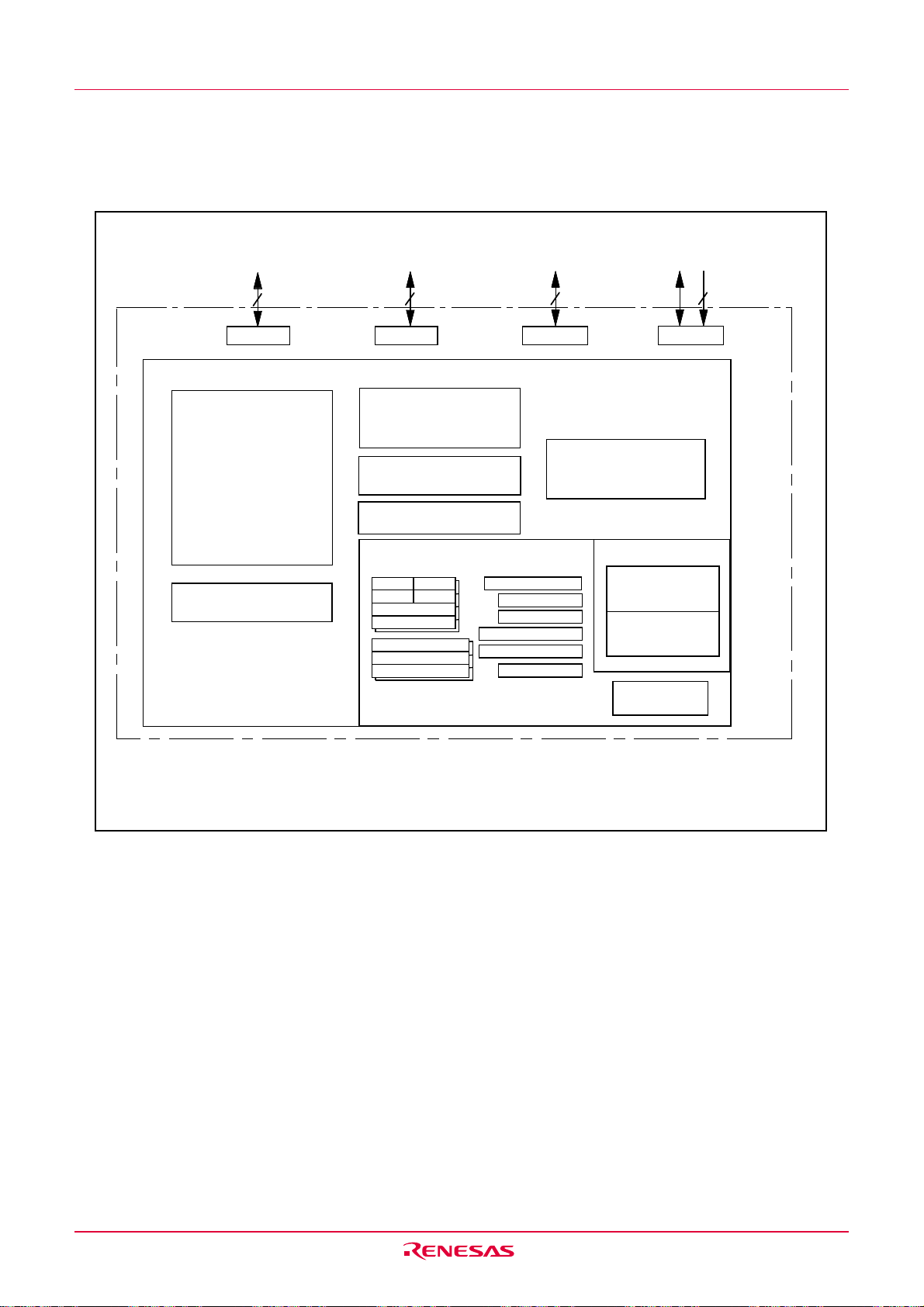
1.3 Block Diagram
Figure 1.1. shows this MCU block diagram.
I / O p o r t
P o r t P 0
Pe r i p h e r a l f u n c t i o n s
T i m e r
T i m e r X ( 8 b i t s )
T i m e r Y ( 8 b i t s )
T i m e r Z ( 8 b i t s )
T i m e r C ( 1 6 b i t s )
Watchdog timer
(15 bits)
ROM
RAM
1 2
Port P4
(1)
(2)
8
8
Port P1
A / D c o n v e r t e r
( 1 0 b i t s ✕ 8 c h a n n e l s )
U A R T o r C l o c k s y n c h r o n o u s
s e r i a l I / O
( 8 b i t s ✕ 1 c h a n n e l )
U A R T
( 8 b i t s ✕ 1 c h a n n e l )
R8C/Tiny Series CPU core
R0LR0H
R1H R1L
R 2
R3
A 0
A1
FB
P o r t P 3
S B
USP
I S P
INTB
PC
FLG
5
System clock generator
I N
- X
O U T
X
O n - c h i p o s c i l l a t o r
M e m o r y
M u l t i p l i e r
Figure 1.1 Block Diagram
NOTES:
1. ROM size depends on MCU type.
2. RAM size depends on MCU type.
Rev.1.20 Jan 27, 2006 page 3 of 181
REJ09B0110-0120
Page 14
R8C/12 Group 1. Overview
1.4 Product Information
Table 1.2 lists the product information.
Table 1.2 Product Information
Type No.
R5F21122FP
R5F21123FP
R5F21124FP
R5F21122DFP
R5F21123DFP
R5F21124DFP
ROM capacity
Program ROM
8K bytes
12K bytes
16K bytes
8K bytes
12K bytes
16K bytes
T y p e N o .R 5 F 2 11 24DF P
Data flash
2K bytes x 2
2K bytes x 2
2K bytes x 2
2K bytes x 2
2K bytes x 2
2K bytes x 2
As of January 2006
RAM capacity
512 bytes
768 bytes
1K bytes
512 bytes
768 bytes
1K bytes
P a c k a g e t y p e :
F P : P L Q P 0 0 3 2 G B - A
C l a s s i f i c a t i o n :
D : O p e r a t i n g a m b i e n t t e m p e r a t u r e – 4 0 ° C t o 8 5 ° C
N o s y m b o l : O p e r a t i n g a m b i e n t t e m p e r a t u r e – 2 0 ° C t o 8 5 ° C
Package type
PLQP0032GB-A
PLQP0032GB-A
PLQP0032GB-A
PLQP0032GB-A
PLQP0032GB-A
PLQP0032GB-A
Flash memory version
D version
Remarks
R O M c a p a c i t y :
2 : 8 K B y t e s .
3 : 1 2 K B y t e s .
4 : 1 6 K B y t e s .
R 8 C /1 2 g r o u p
R 8 C / T i n y s e r i e s
Memory type:
F: Flash memory version
R e n e s a s M C U
R e n e s a s s e m i c o n d u c t o r s
Figure 1.2 Type No., Memory Size, and Package
Rev.1.20 Jan 27, 2006 page 4 of 181
REJ09B0110-0120
Page 15
R8C/12 Group 1. Overview
p
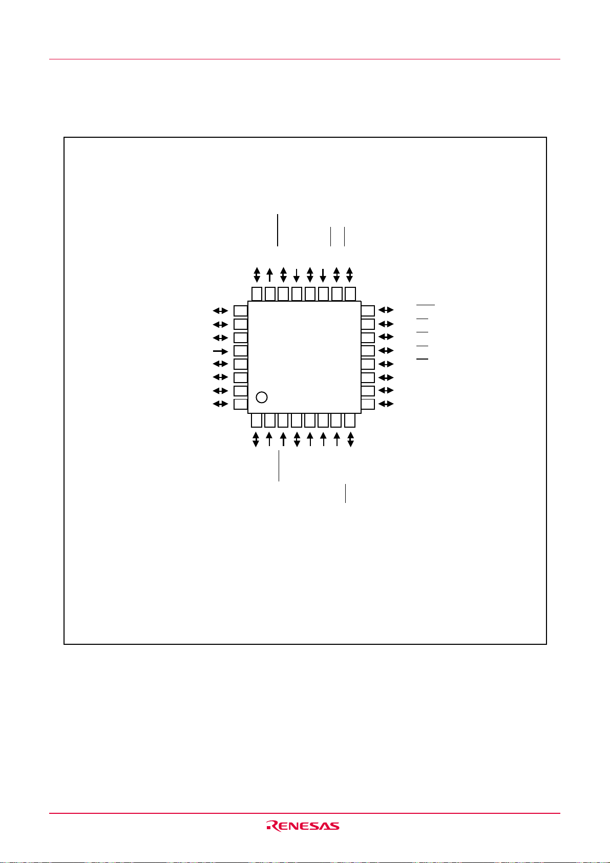
1.5 Pin Assignments
Figure 1.3 shows the pin configuration (top view).
PIN CONFIGURATION (top view)
1
R
N
I
C
F
/
/
3
2
R
T
T
V
/
C
/
/
C
3
2
3
3
V
I N
I N
T
C N T
P
P
A
1 6
1 4
1 3
1 2
1 0
P45/INT
1 5
P10/KI
P11/KI
P12/KI
P13/KI
1 1
P14/TxD
P15/RxD
9
P16/CLK
0
0
1
2
3
0
0
0
P 06/ A N
P05/AN
P 04/ A N
M O D E
P03/AN
P02/AN
P01/AN
P00/AN7/TxD
0
T
R
0
)
N
(
3
/
C
7
C
0
V
C N T
I
A
P
O
Z
S
/
/
S
0
1
3
V
3
P
T
E
P
A
U
2 4 2 3 2 2 2 1 2 0 1 9 1 8 1 7
1
2
3
4
5
6
11
2 5
2 6
2 7
2 8
2 9
3 0
3 1
3 2
R8C/12 Group
1 2 3 4 5 6 7 8
T x
R x
P
N O T E S :
1 . P 4
2 . W h e n u s i n g o n - c h i p d e b u g g e r , d o n o t u s e
3 . D o n o t c o n n e c t I V c c t o V c c .
Figure 1.3 Pin Configuration (Top View)
)
6
1
S
S
D
V
/
0
C
E S E
1
D
N
/
7
3
P
7
f u n c t i o n s o n l y a s a n i n p u t p o r t .
0
0
/ A N7/ T x D
S
T
(
1
S
7
V
4
/
P
T
R
O
X
U
P
1 1
a n d P 37/ T x D
0
C
4
C
R
V
/
N
I
X
/
1
T
/
7
1
P
I N
C N T
1 0
Package: PLQP0032GB-A (32P6U-A)
/ R x D1.
Rev.1.20 Jan 27, 2006 page 5 of 181
REJ09B0110-0120
Page 16

R8C/12 Group 1. Overview
1.6 Pin Description
Table 1.3 shows the pin description
Table 1.3 Pin description
Signal name Pin name I/O type
Power supply Vcc, I
input Vss
IVcc IVcc O
Apply 2.7 V to 5.5 V to the Vcc pin. Apply 0 V to the
Vss pin.
This pin is to stabilize internal power supply.
Connect this pin to Vss via a capacitor (0.1 µF).
Do not connect to Vcc.
Analog power AVcc, I
supply input AVss
Reset input
___________
RESET I
CNVss CNVss I
MODE MODE I
Main clock input XIN I
Power supply input pins for A/D converter. Connect the
AVcc pin to Vcc. Connect the AVss pin to Vss. Connect a
capacitor between pins AVcc and AVss.
Input “L” on this pin resets the MCU.
Connect this pin to Vss via a resistor.
Connect this pin to Vcc via a resistor.
These pins are provided for the main clock generating circuit I/O. Connect a ceramic resonator or a crys-
Main clock output XOUT O
tal oscillator between the XIN and XOUT pins. To use
an externally derived clock, input it to the XIN pin and
_____
INT interrupt input
Key input interrupt
Timer X CNTR0 I/O
_______ _______
INT0 to INT3 I
_____ _____
KI0 to KI3 I
__________
CNTR0 O
Timer Y CNTR1 I/O
Timer Z TZOUT O
Timer C TCIN I
Serial interface CLK0 I/O
RxD0, RxD1 I
TxD0, TxD10,O
leave the XOUT pin open.
______
INT interrupt input pins.
Key input interrupt pins.
Timer X I/O pin
Timer X output pin
Timer Y I/O pin
Timer Z output pin
Timer C input pin
Transfer clock I/O pin.
Serial data input pins.
Serial data output pins.
TxD11
Reference voltage VREF I
input
A/D converter AN0 to AN7 I
I/O port P00 to P07, I/O
P10 to P17,
P30 to P33, P37,
P45
Reference voltage input pin for A/sD converter. Connect the VREF pin to Vcc.
Analog input pins for A/D converter
These are 8-bit CMOS I/O ports. Each port has an
input/output select direction register, allowing each
pin in that port to be directed for input or output individually.
Any port set to input can select whether to use a pullup resistor or not by program.
P10 to P17 also function as LED drive ports.
Input port P46, P47 I
Port for input-only.
NOTES :
1. Refer to "19.8 Noise" for the connecting reference resistor value.
Function
(1)
Rev.1.20 Jan 27, 2006 page 6 of 181
REJ09B0110-0120
Page 17
R8C/12 Group 2. Central Processing Unit (CPU)
2. Central Processing Unit (CPU)
Figure 2.1 shows the CPU registers. The CPU has 13 registers. Of these, R0, R1, R2, R3, A0, A1 and FB
comprise a register bank. Two sets of register banks are provided.
b31
R2
R 3
b19
b15 b8 b7 b0
R 0 H ( h i g h - o r d e r o f R 0 )
R1H(high-order of R1)
b15 b0
INTBH
T h e 4 - h i g h o r d e r b i t s o f I N T B a r e I N T B H a n d
t h e 1 6 - l o w b i t s o f I N T B a r e I N T B L .
b 1 9
b15 b0
b15 b 0
b15 b 0 b7 b 8
I P L
R0L(low-order of R0)
R1L(low-order of R1)
R 2
R 3
A 0
A 1
F B
INTBL
PC
USP
ISP
SB
F L G
D a t a r e g i s t e r s
A d d r e s s r e g i s t e r s
F r a m e b a s e r e g i s t e r s
I n t e r r u p t t a b l e r e g i s t e r
b0
P r o g r a m c o u n t e r
User stack pointer
I n t e r r u p t s t a c k p o i n t e r
Static base regist er
F l a g r e g i s t e r
CDZSBOIU
C a r r y f l a g
Debug flag
Zero flag
S i g n f l a g
R e g i s t e r b a n k s e l e c t f l a g
O v e r f l o w f l a g
I n t e r r u p t e n a b l e f l a g
S t a c k p o i n t e r s e l e c t f l a g
Reserved bit
P r o c e s s o r i n t e r r u p t p r i o r i t y l e v e l
R e s e r v e d b i t
( 1 )
( 1 )
( 1 )
N O T E S :
1 . A r e g i s t e r b a n k c o m p r i s e s t h e s e r e g i s t e r s . T w o s e t s o f r e g i s t e r b a n k s a r e p r o v i d e d
Figure 2.1 CPU Register
2.1 Data Registers (R0, R1, R2 and R3)
R0 is a 16-bit register for transfer, arithmetic and logic operations. The same applies to R1 to R3. The
R0 can be split into high-order bit (R0H) and low-order bit (R0L) to be used separately as 8-bit data
registers. The same applies to R1H and R1L as R0H and R0L. R2 can be combined with R0 to be
used as a 32-bit data register (R2R0). The same applies to R3R1 as R2R0.
Rev.1.20 Jan 27, 2006 page 7 of 181
REJ09B0110-0120
Page 18

R8C/12 Group 2. Central Processing Unit (CPU)
2.2 Address Registers (A0 and A1)
A0 is a 16-bit register for address register indirect addressing and address register relative addressing.
They also are used for transfer, arithmetic and logic operations. The same applies to A1 as A0. A0 can
be combined with A0 to be used as a 32-bit address register (A1A0).
2.3 Frame Base Register (FB)
FB is a 16-bit register for FB relative addressing.
2.4 Interrupt Table Register (INTB)
INTB is a 20-bit register indicates the start address of an interrupt vector table.
2.5 Program Counter (PC)
PC, 20 bits wide, indicates the address of an instruction to be executed.
2.6 User Stack Pointer (USP) and Interrupt Stack Pointer (ISP)
The stack pointer (SP), USP and ISP, are 16 bits wide each. The U flag of FLG is used to switch
between USP and ISP.
2.7 Static Base Register (SB)
SB is a 16-bit register for SB relative addressing.
2.8 Flag Register (FLG)
FLG is a 11-bit register indicating the CPU state.
2.8.1 Carry Flag (C)
The C flag retains a carry, borrow, or shift-out bit that has occurred in the arithmetic logic unit.
2.8.2 Debug Flag (D)
The D flag is for debug only. Set to “0”.
2.8.3 Zero Flag (Z)
The Z flag is set to “1” when an arithmetic operation resulted in 0; otherwise, “0”.
2.8.4 Sign Flag (S)
The S flag is set to “1” when an arithmetic operation resulted in a negative value; otherwise, “0”.
2.8.5 Register Bank Select Flag (B)
The register bank 0 is selected when the B flag is “0”. The register bank 1 is selected when this flag
is set to “1”.
2.8.6 Overflow Flag (O)
The O flag is set to “1” when the operation resulted in an overflow; otherwise, “0”.
2.8.7 Interrupt Enable Flag (I)
The I flag enables a maskable interrupt.
An interrupt is disabled when the I flag is set to “0”, and are enabled when the I flag is set to “1”. The
I flag is set to “0” when an interrupt request is acknowledged.
2.8.8 Stack Pointer Select Flag (U)
ISP is selected when the U flag is set to “0”, USP is selected when the U flag is set to “1”.
The U flag is set to “0” when a hardware interrupt request is acknowledged or the INT instruction of
software interrupt numbers 0 to 31 is executed.
2.8.9 Processor Interrupt Priority Level (IPL)
IPL, 3 bits wide, assigns processor interrupt priority levels from level 0 to level 7.
If a requested interrupt has greater priority than IPL, the interrupt is enabled.
2.8.10 Reserved Bit
When write to this bit, set to “0”. When read, its content is indeterminate.
Rev.1.20 Jan 27, 2006 page 8 of 181
REJ09B0110-0120
Page 19
R8C/12 Group 3. Memory
s
s
s
3. Memory
Figure 3.1 is a memory map of this MCU. This MCU provides 1-Mbyte address space from addresses
0000016 to FFFFF16.
The internal ROM (program ROM) is allocated lower addresses beginning with address 0FFFF16. For
example, a 16-Kbyte internal ROM is allocated addresses from 0C00016 to 0FFFF16.
The fixed interrupt vector table is allocated addresses 0FFDC16 to 0FFFF16. They store the starting
address of each interrupt routine.
The internal ROM (data flash) is allocated addresses from 0200016 to 02FFF16.
The internal RAM is allocated addresses beginning with address 0040016. For example, a 1-Kbyte internal RAM is allocated addresses 0040016 to 007FF16. The internal RAM is used not only for storing data,
but for calling subroutines and stacks when interrupt request is acknowledged.
Special function registers (SFR) are allocated addresses 0000016 to 002FF16. The peripheral function
control registers are located them. All addresses, which have nothing allocated within the SFR, are reserved area and cannot be accessed by users.
0 0 0 0 0
1 6
( S e e C h a p t e r 4 f o r d e t a i l s . )
0 0 2 F F
1 6
00400
16
I n t e r n a l R A M
0 X X X X
1 6
0 2 0 0 0
1 6
I n t e r n a l R O M
( d a t a f l a s h )
0 2 F F F
1 6
0 Y Y Y Y
1 6
I n t e r n a l R O M
0 F F F F
F F F F F
( p r o g r a m R O M )
1 6
E x p a n s i o n a r e a
1 6
N O T E S :
1 . T h e d a t a f l a s h b l o c k A ( 2 K b y t e s ) a n d b l o c k B ( 2 K b y t e s ) a r e s h o w n .
2 . B l a n k s p a c e a r e r e s e r v e d . N o a c c e s s i s a l l o w e d .
T y p e n a m e
R 5 F 2 1 1 2 4 F P , R 5 F 2 1 1 2 4 D F P
R 5 F 2 1 1 2 3 F P , R 5 F 2 1 1 2 3 D F P
R 5 F 2 1 1 2 2 F P , R 5 F 2 1 1 2 2 D F P
S F R
(1 )
Internal ROM
S i z e
16K bytes
12K bytes
8K bytes
0FFDC
16
0FFFF
16
Address 0YYYY
0C000
16
0D000
16
0E000
16
U n d e f i n e d i n s t r u c t i o n
Overflow
B R K i n s t r u c t i o n
Address match
W a t c h d o g t i m e r • O s c i l l a t i o n s t o p d e t e c t i o n
Single step
(Reserved)
(Reserved)
R e s e t
Internal RAM
16
S i z e
1 K b y t e
7 6 8 b y t e
5 1 2 b y t e
A d d r e s s 0 X X X X
007FF
006FF
005FF
1 6
16
16
16
Figure 3.1 Memory Map
Rev.1.20 Jan 27, 2006 page 9 of 181
REJ09B0110-0120
Page 20

R8C/12 Group 4. Special Function Register (SFR)
4. Special Function Register (SFR)
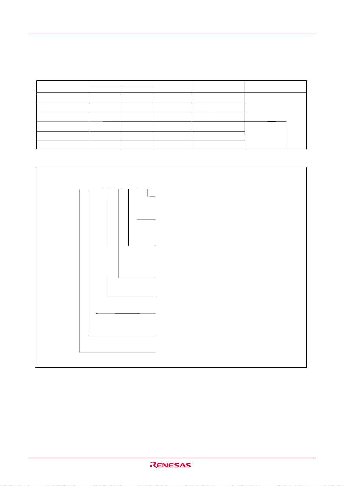
SFR(Special Function Register) is the control register of peripheral functions. Tables 4.1 to 4.4 list the SFR
information
Table 4.1 SFR Information(1)
A d d r e s s
0 0 0 0
1 6
0 0 0 1
1 6
0 0 0 2
1 6
0 0 0 3
1 6
M
X X
0 0 0 4
1 6
P r o c e s s o r m o d e r e g i s t e r 0P
0 0 0 5
1 6
Processor mode register 1 PM1 00XXX0X0
M
1 1 0 1 0 0
0 0 0 6
1 6
S y s t e m c l o c k c o n t r o l r e g i s t e r 0C
M
0 1 0 0 0 0
0 0 0 7
1 6
S y s t e m c l o c k c o n t r o l r e g i s t e r 1C
0 0 0 8
1 6
I E
X X X X X 0
0 0 0 9
1 6
A d d r e s s m a t c h i n t e r r u p t e n a b l e r e g i s t e rA
0 0 0 A
1 6
Protect register PRCR 00XXX000
0 0 0 B
1 6
C
0 0 0 0 1 0
0 0 0 C
1 6
O s c i l l a t i o n s t o p d e t e c t i o n r e g i s t e rO
D T
0 0 0 D
1 6
W a t c h d o g t i m e r r e s e t r e g i s t e rW
0 0 0 E
1 6
Watchdog timer start register WDTS XX
D
0 0 1 1 1 1
0 0 0 F
1 6
W a t c h d o g t i m e r c o n t r o l r e g i s t e rW
M A D
0 0 1 0
1 6
A d d r e s s m a t c h i n t e r r u p t r e g i s t e r 0R
0 0 1 1
1 6
0 0 1 2
1 6
0 0 1 3
1 6
M A D
0 0 1 4
1 6
A d d r e s s m a t c h i n t e r r u p t r e g i s t e r 1R
0 0 1 5
1 6
0 0 1 6
1 6
0 0 1 7
1 6
0 0 1 8
1 6
0 0 1 9
1 6
0 0 1 A
1 6
0 0 1 B
1 6
0 0 1 C
1 6
0 0 1 D
1 6
N T 0
X X X X 0 0
0 0 1 E
1 6
I N T 0 i n p u t f i l t e r s e l e c t r e g i s t e rI
0 0 1 F
1 6
0 0 2 0
1 6
0 0 2 1
1 6
0 0 2 2
1 6
0 0 2 3
1 6
0 0 2 4
1 6
0 0 2 5
1 6
0 0 2 6
1 6
0 0 2 7
1 6
0 0 2 8
1 6
0 0 2 9
1 6
0 0 2 A
1 6
0 0 2 B
1 6
0 0 2 C
1 6
0 0 2 D
1 6
0 0 2 E
1 6
0 0 2 F
1 6
0 0 3 0
1 6
0 0 3 1
1 6
0 0 3 2
1 6
0 0 3 3
1 6
0 0 3 4
1 6
0 0 3 5
1 6
0 0 3 6
1 6
0 0 3 7
1 6
0 0 3 8
1 6
0 0 3 9
1 6
0 0 3 A
1 6
0 0 3 B
1 6
0 0 3 C
1 6
0 0 3 D
1 6
0 0 3 E
1 6
0 0 3 F
1 6
N O T E S :
1 . B l a n k s p a c e s a r e r e s e r v e d . N o a c c e s s i s a l l o w e d .
X : U n d e f i n e d
(1)
Register Symbol After reset
0X
00
10
X0X 0 0
0
0
RX
D0
RX
C0
00
0 0
X 0
10
0 0
X 0
0
X
1 6
16
1
0
1 6
1 6
1 6
0
1 6
1 6
1 6
FX
2
2
2
2
0
2
2
2
2
0
2
Rev.1.20 Jan 27, 2006 page 10 of 181
REJ09B0110-0120
Page 21

R8C/12 Group 4. Special Function Register (SFR)
Table 4.2 SFR Information(2)
A d d r e s s
0 0 4 0
1 6
0 0 4 1
1 6
0 0 4 2
1 6
0 0 4 3
1 6
0 0 4 4
1 6
0 0 4 5
1 6
0 0 4 6
1 6
0 0 4 7
1 6
0 0 4 8
1 6
0 0 4 9
1 6
0 0 4 A
1 6
0 0 4 B
1 6
0 0 4 C
1 6
U P I
X X X X 0 0
0 0 4 D
1 6
K e y i n p u t i n t e r r u p t c o n t r o l r e g i s t e rK
D I
X X X X 0 0
0 0 4 E
1 6
A D c o n v e r s i o n i n t e r r u p t c o n t r o l r e g i s t e rA
0 0 4 F
1 6
0 0 5 0
1 6
0 0 5 1
1 6
UART0 transmit interrupt control register
X X X X 0 0
0 0 5 2
1 6
U A R T 0 r e c e i v e i n t e r r u p t c o n t r o l r e g i s t e r
X X X X 0 0
0 0 5 3
1 6
U A R T 1 t r a n s m i t i n t e r r u p t c o n t r o l r e g i s t e r
X X X X 0 0
0 0 5 4
1 6
U A R T 1 r e c e i v e i n t e r r u p t c o n t r o l r e g i s t e r
0 0 5 5
1 6
INT2 interrupt contro l register INT2IC XXXXX000
X I
X X X X 0 0
0 0 5 6
1 6
T i m e r X i n t e r r u p t c o n t r o l r e g i s t e rT
Y I
X X X X 0 0
0 0 5 7
1 6
T i m e r Y i n t e r r u p t c o n t r o l r e g i s t e rT
Z I
X X X X 0 0
0 0 5 8
1 6
T i m e r Z i n t e r r u p t c o n t r o l r e g i s t e rT
0 0 5 9
1 6
INT1 interrupt contro l register INT1IC XXXXX000
0 0 5 A
1 6
INT3 interrupt contro l register INT3IC XXXXX000
C I
X X X X 0 0
0 0 5 B
1 6
T i m e r C i n t e r r u p t c o n t r o l r e g i s t e rT
0 0 5 C
1 6
N T 0 I
X 0 0 X 0 0
0 0 5 D
1 6
I N T 0 i n t e r r u p t c o n t r o l r e g i s t e rI
0 0 5 E
1 6
0 0 5 F
1 6
0060
16
0061
16
0062
16
0063
16
0064
16
0065
16
0066
16
0067
16
0068
16
0069
16
006A
16
006B
16
006C
16
006D
16
006E
16
006F
16
0070
16
0071
16
0072
16
0073
16
0074
16
0075
16
0076
16
0077
16
0078
16
0079
16
007A
16
007B
16
007C
16
007D
16
007E
16
007F
16
N O T E S :
1 . B l a n k s p a c e s a r e r e s e r v e d . N o a c c e s s i s a l l o w e d .
(1)
R e g i s t e rS
X : U n d e f i n e d
y m b o l
A
CX
CX
f t e r r e s e
t
0
0
S0TIC XXXXX000
S 0 R I CX
S 1 T I CX
S 1 R I CX
CX
CX
CX
CX
CX
0
0
0
0
0
0
0
0
2
2
2
2
2
2
2
2
2
2
2
2
2
2
Rev.1.20 Jan 27, 2006 page 11 of 181
REJ09B0110-0120
Page 22

R8C/12 Group 4. Special Function Register (SFR)
Table 4.3 SFR Information(3)
A d d r e s s
N O T E S :
1 . B l a n k s p a c e s a r e r e s e r v e d . N o a c c e s s i s a l l o w e d .
Y Z M
0 0 8 0
1 6
T i m e r Y , Z m o d e r e g i s t e rT
R E
0 0 8 1
1 6
P r e s c a l e r Y r e g i s t e rP
Y S
0 0 8 2
1 6
T i m e r Y s e c o n d a r y r e g i s t e rT
Y P
0 0 8 3
1 6
T i m e r Y p r i m a r y r e g i s t e rT
U
0 0 8 4
1 6
T i m e r Y , Z w a v e f o r m o u t p u t c o n t r o l r e g i s t e rP
R E
0 0 8 5
1 6
P r e s c a l e r Z r e g i s t e rP
Z S
0 0 8 6
1 6
T i m e r Z s e c o n d a r y r e g i s t e rT
Z P
0 0 8 7
1 6
T i m e r Z p r i m a r y r e g i s t e rT
0 0 8 8
1 6
0 0 8 9
1 6
Y Z O
T i m e r Y , Z o u t p u t c o n t r o l r e g i s t e rT
0 0 8 A
1 6
X M
T i m e r X m o d e r e g i s t e rT
0 0 8 B
1 6
R E
P r e s c a l e r X r e g i s t e rP
0 0 8 C
1 6
T i m e r X r e g i s t e rT
0 0 8 D
1 6
C S
T i m e r c o u n t s o u r c e s e t t i n g r e g i s t e rT
0 0 8 E
1 6
0 0 8 F
1 6
0 0 9 0
1 6
T i m e r C r e g i s t e rT
0 0 9 1
1 6
0 0 9 2
1 6
0 0 9 3
1 6
0 0 9 4
1 6
0 0 9 5
1 6
N T E
0 0 9 6
1 6
E x t e r n a l i n p u t e n a b l e r e g i s t e rI
0 0 9 7
1 6
I E
K e y i n p u t e n a b l e r e g i s t e rK
0 0 9 8
1 6
0 0 9 9
1 6
C C
T i m e r C c o n t r o l r e g i s t e r 0T
0 0 9 A
1 6
C C
T i m e r C c o n t r o l r e g i s t e r 1T
0 0 9 B
1 6
M
0 0 9 C
1 6
C a p t u r e r e g i s t e rT
0 0 9 D
1 6
0 0 9 E
1 6
0 0 9 F
1 6
0 0 A 0
1 6
U A R T 0 t r a n s m i t / r e c e i v e m o d e r e g i s t e r
0 B R
0 0 A 1
1 6
U A R T 0 b i t r a t e r e g i s t e r U
0 T
0 0 A 2
1 6
U A R T 0 t r a n s m i t b u f f e r r e g i s t e rU
0 0 A 3
1 6
0 0 0 1 0 0
0 0 A 4
1 6
U A R T 0 t r a n s m i t / r e c e i v e c o n t r o l r e g i s t e r 0
0 0 0 0 0 1
0 0 A 5
1 6
U A R T 0 t r a n s m i t / r e c e i v e c o n t r o l r e g i s t e r 1
0 R
0 0 A 6
1 6
U A R T 0 r e c e i v e b u f f e r r e g i s t e r U
0 0 A 7
1 6
0 0 A 8
1 6
U A R T 1 t r a n s m i t / r e c e i v e m o d e r e g i s t e r
1 B R
0 0 A 9
1 6
U A R T 1 b i t r a t e g e n e r a t o rU
1 T
0 0 A A
1 6
U A R T 1 t r a n s m i t b u f f e r r e g i s t e rU
0 0 A B
1 6
0 0 0 1 0 0
0 0 A C
1 6
U A R T 1 t r a n s m i t / r e c e i v e c o n t r o l r e g i s t e r 0
0 0 0 0 0 1
0 0 A D
1 6
U A R T 1 t r a n s m i t / r e c e i v e c o n t r o l r e g i s t e r 1
1 R
0 0 A E
1 6
U A R T 1 r e c e i v e b u f f e r r e g i s t e r U
0 0 A F
1 6
0 0 B 0
1 6
U A R T t r a n s m i t / r e c e i v e c o n t r o l r e g i s t e r 2
0 0 B 1
1 6
0 0 B 2
1 6
0 0 B 3
1 6
0 0 B 4
1 6
0 0 B 5
1 6
0 0 B 6
1 6
0 0 B 7
1 6
0 0 B 8
1 6
0 0 B 9
1 6
0 0 B A
1 6
0 0 B B
1 6
0 0 B C
1 6
0 0 B D
1 6
0 0 B E
1 6
0 0 B F
1 6
(1)
R e g i s t e rS
X : U n d e f i n e d
y m b o l
A
R0
YF
CF
RF
M0
ZF
CF
RF
C0
R0
XF
XF
S0
C0
N0
N0
00
10
00
U 0 M R0
GX
BX
U 0 C 00
U 0 C 10
BX
U 1 M R0
GX
BX
U 1 C 00
U 1 C 10
BX
U C O N0
0 0
0 0
X X
X X
X X
X X
f t e r r e s e
1 6
0
F
1 6
F
1 6
F
1 6
0
1 6
F
1 6
F
1 6
F
1 6
0
1 6
0
1 6
F
1 6
F
1 6
0
1 6
0
1 6
1 6
0
1 6
0
1 6
0
1 6
0
1 6
0
1 6
1 6
0
1 6
X
1 6
X
1 6
1 6
0
0
X
1 6
1 6
0
1 6
X
1 6
X
1 6
1 6
0
0
X
1 6
1 6
0
1 6
t
2
2
2
2
Rev.1.20 Jan 27, 2006 page 12 of 181
REJ09B0110-0120
Page 23

R8C/12 Group 4. Special Function Register (SFR)
Table 4.4 SFR Information(4)
A d d r e s s
X X X X X X
0 0 C 0
1 6
A D r e g i s t e rA
0 0 C 1
1 6
0 0 C 2
1 6
0 0 C 3
1 6
0 0 C 4
1 6
0 0 C 5
1 6
0 0 C 6
1 6
0 0 C 7
1 6
0 0 C 8
1 6
0 0 C 9
1 6
0 0 C A
1 6
0 0 C B
1 6
0 0 C C
1 6
0 0 C D
1 6
0 0 C E
1 6
0 0 C F
1 6
0 0 D 0
1 6
0 0 D 1
1 6
0 0 D 2
1 6
0 0 D 3
1 6
D C O N
0 0 D 4
1 6
A D c o n t r o l r e g i s t e r 2A
0 0 D 5
1 6
D C O N
0 0 0 0 X X
0 0 D 6
1 6
A D c o n t r o l r e g i s t e r 0A
D C O N
0 0 D 7
1 6
A D c o n t r o l r e g i s t e r 1 A
0 0 D 8
1 6
0 0 D 9
1 6
0 0 D A
1 6
0 0 D B
1 6
0 0 D C
1 6
0 0 D D
1 6
0 0 D E
1 6
0 0 D F
1 6
00E0
16
P o r t P 0 r e g i s t e rP
00E1
16
P o r t P 1 r e g i s t e rP
00E2
16
Port P0 direction register PD0 00
00E3
16
Port P1 direction register PD1 00
00E4
16
00E5
16
P o r t P 3 r e g i s t e rP
00E6
16
D
00E7
16
P o r t P 3 d i r e c t i o n r e g i s t e rP
00E8
16
P o r t P 4 r e g i s t e rP
00E9
16
D
00EA
16
P o r t P 4 d i r e c t i o n r e g i s t e rP
00EB
16
00EC
16
00ED
16
00EE
16
00EF
16
00F0
16
00F1
16
00F2
16
00F3
16
00F4
16
00F5
16
00F6
16
00F7
16
00F8
16
00F9
16
03FA
16
00FB
16
U R
0 X X 0 0 0
00FC
16
P u l l - u p c o n t r o l r e g i s t e r 0 P
00FD
16
Pull-up control register 1 PUR1 XXXXXX0X
R
00FE
16
P o r t P 1 d r i v e c a p a c i t y c o n t r o l r e g i s t e r D
00FF
16
R e g i s t e r
(1)
S y m b o lA
DX
0X
1X
f t e r r e s e
X X X X X X X X
20
0
1 6
00
10
0
1 6
X
1 6
X
1 6
X
2
2
X
2
16
16
3X
30
4X
40
00
R0
X
1 6
0
1 6
X
1 6
0
1 6
0
2
0
2
1 6
t
01B3
16
Flash memory control register 4 FMR4 01000000
01B4
16
01B5
16
Flash memory control register 1 FMR1 1000000X
01B6
16
M R
0 0 0 0 0 0
01B7
16
F l a s h m e m o r y c o n t r o l r e g i s t e r 0 F
( 2 )
1 6
a n d 0 1 B 8
1 6
t o 0 2 F F
1 6
a r e a l l r e s e r v e d . N o a c c e s s i s a l l o w e d .
0 F F F F
1 6
O p t i o n f u n c t i o n s e l e c t r e g i s t e r
N O T E S :
1 . B l a n k c o l u m n s , 0 1 0 0
2 . T h e w a t c h d o g t i m e r c o n t r o l b i t i s a s s i g n e d . R e f e r t o " F i g u r e 1 1 . 2 O F S , W D C , W D T R a n d W D T S r e g i s t e r s " f o r t h e O F S r e g i s t e r d e t a i l s
X : U n d e f i n e d
1 6
t o 0 1 B 2
00
O F S
( N o t e 2 )
Rev.1.20 Jan 27, 2006 page 13 of 181
REJ09B0110-0120
2
2
1
2
Page 24

R8C/12 Group 5. Reset
5. Reset
There are three types of resets: a hardware reset, a software reset, and an watchdog timer reset.
5.1 Hardware Reset
A reset is applied using the RESET pin. When an “L” signal is applied to the RESET pin while
the power supply voltage is within the recommended operating condition, the pins are initialized (see Table 5.1 “Pin Status When RESET Pin Level is 'L'”). When the input level at the
____________
RESET pin is released from “L” to “H”, the CPU and SFR are initialized, and the program is
executed starting from the address indicated by the reset vector. Figure 5.1 shows the CPU
register status after reset and figure 5.2 shows the reset sequence. After reset, the on-chip
oscillator clock divided by 8 is automatically selected for the CPU. The internal RAM is not
initialized. If the RESET pin is pulled “L” while writing to the internal RAM, the internal RAM
becomes indeterminate. Figures 5.3 to 5.4 show the reset circuit example. Refer to Chapter 4,
“Special Function Register (SFR)” for the status of SFR after reset.
____________
____________ ____________
____________
• When the power supply is stable
____________
(1) Apply an “L” signal to the RESET pin.
(2) Wait for 500 µs (1/fRING ✕ 20).
____________
(3) Apply an “H” signal to the RESET pin.
• Power on
____________
(1) Apply an “L” signal to the RESET pin.
(2) Let the power supply voltage increase until it meets the recommended operating condition.
(3) Wait td(P-R) or more until the internal power supply stabilizes.
(4) Wait for 500 µs (1/fRING ✕ 20).
____________
(5) Apply an “H” signal to the RESET pin.
Table 5.1 Pin Status When RESET Pin Level is “L”
____________
Pin name
P0
P1
0
to P33, P3
P3
P45
to P47
7
Input port
Input port
Input port
Input port
Status
5.2 Software Reset When the PM03 bit in the PM0 register is set to “1” (microcomputer reset), the microcomputer has its
pins, CPU, and SFR initialized. Then the program is executed starting from the address indicated by
the reset vector. After reset, the on-chip oscillator clock divided by 8 is automatically selected for the
CPU.
5.3 Watchdog Timer Reset
Where the PM12 bit in the PM1 register is “1” (reset when watchdog timer underflows), the microcomputer initializes its pins, CPU and SFR if the watchdog timer underflows. Then the program is executed starting from the address indicated by the reset vector. After reset, the on-chip oscillator clock
divided by 8 is automatically selected for the CPU.
Rev.1.20 Jan 27, 2006 page 14 of 181
REJ09B0110-0120
Page 25
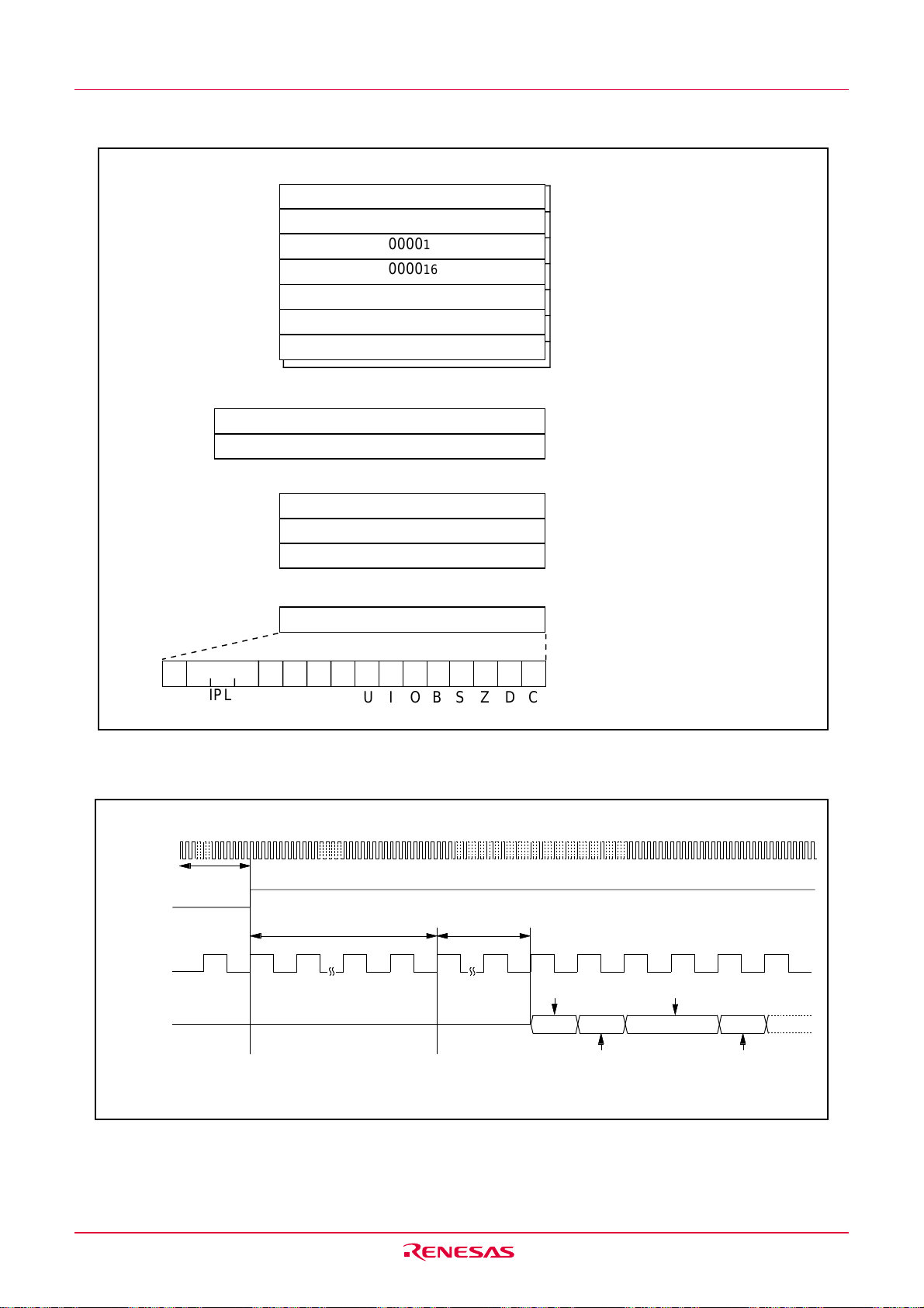
R8C/12 Group 5. Reset
b15
000016
000016
000016
000016
000016
000016
000016
b19
0000016
Content of addresses 0FFFE16 to 0FFFC16
b15
16
0000
000016
000016
b15
0000
16
b0
Data register(R0)
Data register(R1)
Data register(R2)
Data register(R3)
Address register(A0)
Address register(A1)
Frame base register(FB)
b0
Interrupt table register(INTB)
Program counter(PC)
b0
User stack pointer(USP)
Interrupt stack pointer(ISP)
Static base register(SB)
b0
Flag register(FLG)
b15
b7 b8
IPL
Figure 5.1 CPU Register Status After Reset
I N
fR
G
I n t e r n a l o n - c h i p
o s c i l l a t i o n
C P U c l o c k
A d d r e s s
( I n t e r n a l a d d r e s s s i g n a l )
N O T E S :
1 . T h i s s h o w s h a r d w a r e r e s e t
M o r e t h a n 2 0 c y c l e s a r e n e e d e d
F l a s h m e m o r y a c t i v a t e d t i m e
( C P U c l o c k ✕ 6 4 c y c l e s )
( 1 )
C P U c l o c k ✕ 2 8 c y c l e s
b0
CDZSBOIU
0 F F F C1
6
0 F F F D
0 F F F E1
6
1 6
C o n t e n t o f r e s e t v e c t o r
Figure 5.2 Reset Sequence
Rev.1.20 Jan 27, 2006 page 15 of 181
REJ09B0110-0120
Page 26
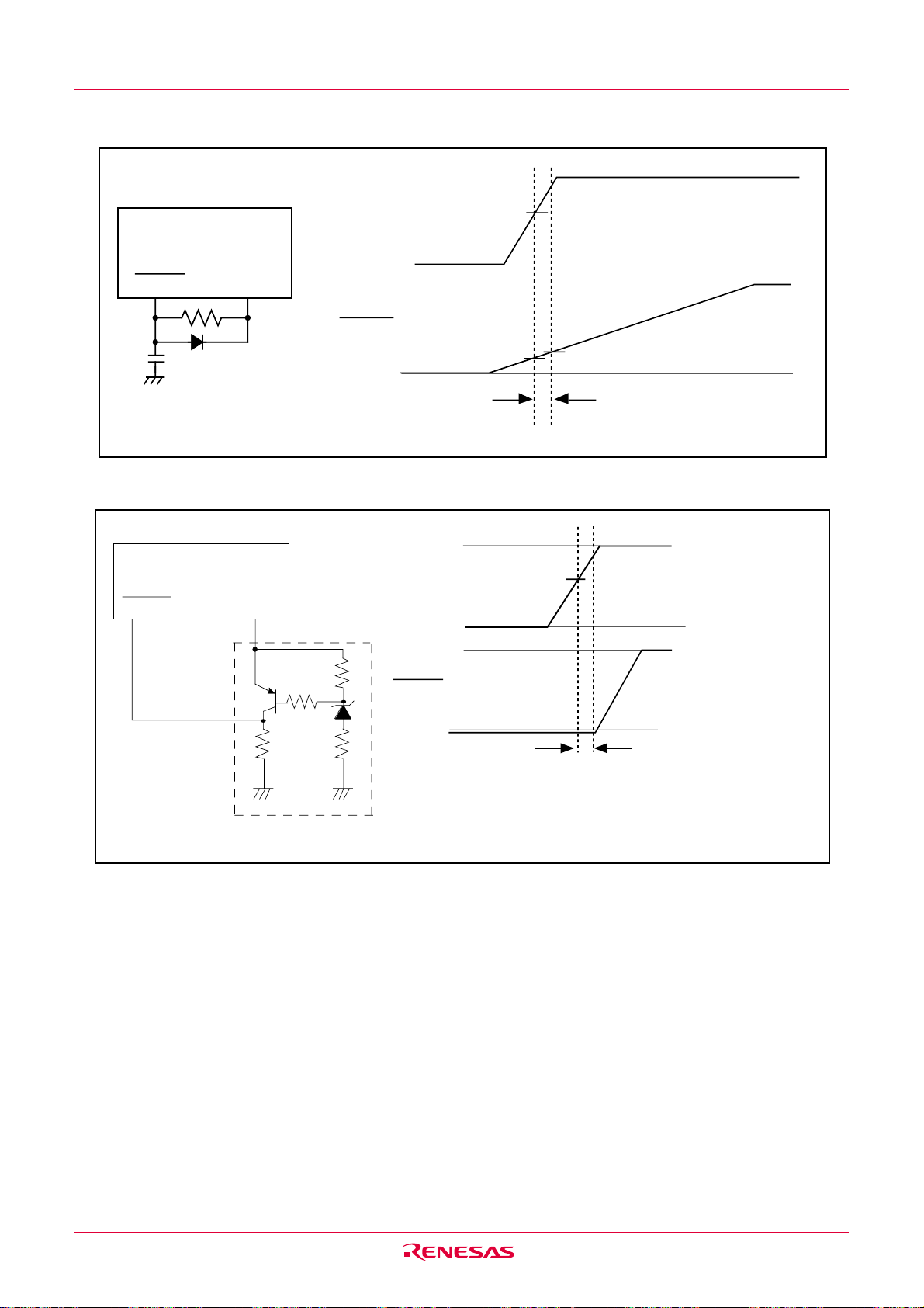
R8C/12 Group 5. Reset
RESET
V
CC
RESET
V
CC
0V
0V
More than td(P-R) + 500 µs are
needed.
Equal to or less
than 0.2V
CC
2.7V
Figure 5.3 Example Reset Circuit
5V
VCC
VCCRESET
Supply voltage
detection circuit
0V
5V
RESET
0V
Example when VCC = 5V.
Figure 5.4 Example Reset Circuit (Voltage Check Circuit)
2.7V
More than td(P-R) + 500 µs
are needed.
Rev.1.20 Jan 27, 2006 page 16 of 181
REJ09B0110-0120
Page 27

R8C/12 Group
p
k
q
y
y
(1 )
p
p p
p
p
p
g
g
6. Clock Generation Circuit
6. Clock Generation Circuit
The clock generation circuit contains two oscillator circuits as follows:
• Main clock oscillation circuit
• On-chip oscillator (with oscillation stop detection function)
Table 6.1 lists the clock generation circuit specifications. Figure 6.1 shows the clock generation circuit.
Figures 6.2 and 6.3 show the clock-related registers.
Table 6.1 Clock Generation Circuit Specifications
I t e m
U s e o f c l o c
u e n c
C l o c k f r e
M a i n c l o c k
o s c i l l a t i o n c i r c u i t
h e r a l f u n c t i o n c l o c k s o u r c
• C P U c l o c k s o u r c e
• P e r i
• CPU and peripheral function
clock sources when the
main clock stops oscillating
0 t o 1 6 M H z
s o s c i l l a t i n
• C P U c l o c k s o u r c e
e
• P e r i p h e r a l f u n c t i o n c l o c k s o u r c e
• C P U a n d p e r i p h e r a l f u n c t i o n
A b o u t 1 2 5 k H z
O n - c h i
o s c i l l a t o r
c l o c k s o u r c e s w h e n t h e m a i n
c l o c k s t o
Usable oscillator
P i n s t o c o n n e c t
• Ceramic resonator
• Cr
stal oscillator
X
I N
, X
O U T
( N o t e 1 )
o s c i l l a t o r
O s c i l l a t i o n s t a r t s
a n d s t o
s
O s c i l l a t o r s t a t u s
Present
e
S t o
Present
d
O s c i l l a t i n
a f t e r r e s e t
u
O t h e r
E x t e r n a l l y d e r i v e d
c l o c k c a n b e i n
t
NOTES:
1. Can be used as P46 and P47 when the on-chip oscillator clock is used for CPU clock
while the main clock oscillation circuit is not used.
Rev.1.20 Jan 27, 2006 page 17 of 181
REJ09B0110-0120
Page 28
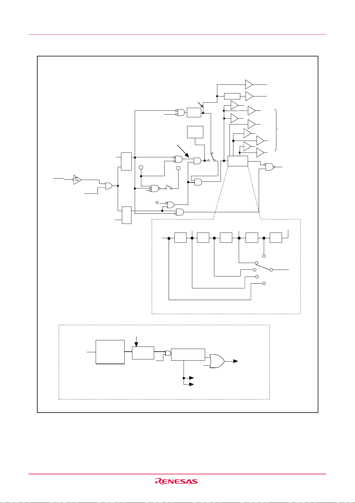
R8C/12 Group
j
k
RQScR
S
R
T
8
0
O
8
8
O
2
k
C M 1 0 = 1 ( S t o p m o d e )
6. Clock Generation Circuit
I N
fR
G
I N G 1 2
O n - c h i p
o s c i l l a t o r
c l o c k
O n - c h i p
M a i n
o s c i l l a t o r
O s c i l l a t i o n
s t o p
d e t e c t i o n
O C D 2 = 1
U
XO
O C D 2 =
C M 1 4
c l o c
Q
XI
N
1 / 1 2
e
b
a
D i v i d e r
fR
f1
S I
f1
fA
D
f
S I
f8
2 S I
f3
P e r i p h e r a l
f u n c t i o n c l o c k
O
f
f3
2
c
d
C P U c l o c k
R E S E T
u d g m e n t o u t p u
I n t e r r u p t r e q u e s t l e v e l
t
W A I T i n s t r u c t i o n
C M 0 2 , C M 0 5 , C M 0 6 : C M 0 r e g i s t e r b i t s
C M 1 0 , C M 1 3 , C M 1 4 , C M 1 6 , C M 1 7 : C M 1 r e g i s t e r b i t s
O C D 0 , O C D 1 , O C D 2 : O C D r e g i s t e r b i t s
O s c i l l a t i o n s t o p d e t e c t i o n c i r c u i t
P u l s e g e n e r a t i o n
M a i n c l o c
c i r c u i t f o r c l o c k
e d g e d e t e c t i o n
a n d c h a r g e ,
d i s c h a r g e c o n t r o l
c i r c u i t
N O T E S :
1 . S e t t h e s a m e v a l u e t o t h e O C D 1 b i t a n d O C D 0 b i t .
C M 1 3
C M 0 5
C M 0 2
a
F o r c i b l e d i s c h a r g e w h e n O C D 0
C h a r g e ,
d i s c h a r g e
c i r c u i t
(1 )
O C D 1
e
1 / 2 1 / 2 1 / 2 1 / 2
C M 0 6 = 0
C M 1 7 t o C M 1 6 = 1 0
C M 0 6 = 0
C M 0 6 = 0
C M 1 7 t o C M 1 6 = 0 0
(1 )
O s c i l l a t i o n s t o p
d e t e c t i o n i n t e r r u p t
g e n e r a t i o n c i r c u i t
W a t c h d o g
t i m e r
i n t e r r u p t
C M 1 7 t o C M 1 6 = 0 1
2
O C D 2 b i t s w i t c h s i g n a l
C M 1 4 b i t s w i t c h s i g n a l
2
b
C M 0 6 = 1
2
O s c i l l a t i o n s t o p
d e t e c t i o n ,
w a t c h d o g t i m e r
i n t e r r u p t
1 / 2
C M 0 6 = 0
C M 1 7 t o C M 1 6 = 1 12
d
D e t a i l s o f d i v i d e r
Figure 6.1 Clock Generation Circuit
Rev.1.20 Jan 27, 2006 page 18 of 181
REJ09B0110-0120
Page 29
R8C/12 Group
6
g
7
3
0
W
0
0
W
W
W
4
W
3
W
W
W
W
6. Clock Generation Circuit
S y s t e m c l o c k c o n t r o l r e g i s t e r 0
b7 b 6b 5b 4b 3b 2b 1b 0
00001
( b 1 - b 0 )
C M 0 2
s t o p m o d e f r o m h i g h o r m i d d l e s p e e d m o d e , t h e C M 0 6 b i t i s s e t t o “ 1 ” ( d i v i d e - b y - 8 m o d e ) .
N O T E S :
( 1 )
d d r e s
0 0
S y m b o lA
C M 00
sA f t e r r e s e t
6
1 6
Bit name F u n c t i o nB i t s y m b o l
R e s e r v e d b i t
W A I T p e r i p h e r a l f u n c t i o n
c l o c k s t o p b i t
( b 3 )
( b 4 )
C M 0 5
CM0
( b 7 )
R e s e r v e d b i t Set to “1”
Reserved bit
M a i n c l o c k ( X
(2 , 4 )
b i t
C P U c l o c k d i v i s i o n s e l e c t
(5 )
b i t 0
I N
- X
O U T
) s t o p
R e s e r v e d b i t Set to “0”
6 8
1 6
Set to “0”
0 : Do not stop peripheral function clock in wait mode
1 : Stop peripheral function clock in wait mode
Set to “0”
0 : On
(3)
1 : Off
0 : CM16 and CM17 valid
1 : Divide-by-8 mode
RW
RW
RW
RW
RW
RW
RW
RW
1 . S e t t h e P R C 0 b i t o f P R C R r e g i s t e r t o “ 1 ” ( w r i t e e n a b l e ) b e f o r e w r i t i n g t o t h i s r e g i s t e r .
2 . T h e C M 0 5 b i t i s p r o v i d e d t o s t o p t h e m a i n c l o c k w h e n t h e o n - c h i p o s c i l l a t o r m o d e i s s e l e c t e d . T h i s b i t c a n n o t b e u s e d f o r d e t e c t i o n a s t o
w h e t h e r t h e m a i n c l o c k s t o p p e d o r n o t . T o s t o p t h e m a i n c l o c k , t h e f o l l o w i n g s e t t i n g i s r e q u i r e d :
( 1 ) S e t t h e O C D 0 a n d O C D 1 b i t s i n t h e O C D r e g i s t e r t o “ 0 0
2
” ( d i s a b l e o s c i l l a t i o n s t o p d e t e c t i o n f u n c t i o n ) .
( 2 ) S e t t h e O C D 2 b i t t o “ 1 ” ( s e l e c t o n - c h i p o s c i l l a t o r c l o c k ) .
3 . S e t t h e C M 0 5 b i t t o “ 1 ” ( m a i n c l o c k s t o p s ) a n d t h e C M 1 3 b i t i n t h e C M 1 r e g i s t e r t o “ 1 ” ( X
4 . W h e n t h e C M 0 5 b i t i s s e t t o “ 1 ” ( m a i n c l o c k s t o p ) , P 4
6
a n d P 4
7
c a n b e u s e d a s i n p u t p o r t s .
5 . W h e n e n t e r i n
I N
- X
O U T
p i n ) w h e n t h e e x t e r n a l c l o c k i s i n p u t .
S y s t e m c l o c k c o n t r o l r e g i s t e r 1
b
b 6b 5b 4b
p i n ) , t h e X O U T ( P
U
P
N O T E S :
b 2b 1b
C M 1 5
C M 1 6
C M 1 7
( 1 )
d d r e s
0 0
S y m b o lA
C M 10
sA f t e r r e s e t
71
6 2
B i t n a m eF
C M 1 0
( b 1 )
( b 2 )
C M 1
C M 1
A l l c l o c k s t o p c o n t r o l
(4 , 6 )
b i t
R e s e r v e d b i t
R e s e r v e d b i t
s w i t c h b i
U
P o r t XI
N-
XO
T
O n - c h i p o s c i l l a t i o n s t o p b i t
d r i v e c a p a c i t y
U
X
I N-
XO
T
(
s e l e c t b i t
C P U c l o c k d i v i s i o n
s e l e c t b i t 1
2 )
(
3 )
0 : C l o c k o n
1 : A l l c l o c k s o f f ( s t o p m o d e )
S e t t o
S e t t o
U
p i
0 : I n p u t p o r t P 46, P 47
(
6 )
t
1 : X
0 : O n - c h i p o s c i l l a t o r o n
1 : O n - c h i p o s c i l l a t o r o f f
0 : L O W
1 : H I G H
b 7 b 6
0 0 : N o d i v i s i o n m o d e
0 1 : D i v i s i o n b y 2 m o d e
1 0 : D i v i s i o n b y 4 m o d e
1 1 : D i v i s i o n b y 1 6 m o d e
01
6
u n c t i o
nB i t s y m b o l
“ 0 ”
“ 0 ”
I N-
XO
T
n
(
5 )
R
R
R
R
R
R
R
R
R
1 . W r i t e t o t h i s r e g i s t e r a f t e r s e t t i n g t h e P R C 0 b i t o f P R C R r e g i s t e r t o “ 1 ” ( w r i t e e n a b l e ) .
2 . W h e n e n t e r i n g s t o p m o d e f r o m h i g h o r m i d d l e s p e e d m o d e , t h e C M 1 5 b i t i s s e t t o “ 1 ” ( d r i v e c a p a c i t y h i g h ) .
3 . E f f e c t i v e w h e n t h e C M 0 6 b i t i s “ 0 ” ( C M 1 6 a n d C M 1 7 b i t s e n a b l e ) .
4 . I f t h e C M 1 0 b i t i s “ 1 ” ( s t o p m o d e ) , t h e i n t e r n a l f e e d b a c k r e s i s t o r b e c o m e s i n e f f e c t i v e .
5 . T h e C M 1 4 b i t c a n b e s e t t o “ 1 ” ( o n - c h i p o s c i l l a t o r o f f ) i f t h e O C D 2 b i t = 0 ( s e l e c t i n g m a i n c l o c k ) . W h e n t h e O C D 2 b i t i s s e t t o “ 1 ”
( s e l e c t i n g o n - c h i p o s c i l l a t o r c l o c k ) , t h e C M 1 4 b i t i s s e t t o “ 0 ” ( o n - c h i p o s c i l l a t o r o n ) . T h i s b i t r e m a i n s u n c h a n g e d w h e n “ 1 ” i s w r i t t e n .
6 . W h e n t h e C M 1 0 b i t i s s e t t o “ 1 ” ( s t o p m o d e ) o r t h e C M 0 5 b i t i n t h e C M 0 r e g i s t e r t o “ 1 ” ( m a i n c l o c k s t o p s ) a n d t h e C M 1 3 b i t i s s e t t o
“ 1 ” ( X
I N-
XO
W h e n t h e C M 1 3 b i t i s s e t t o “ 0 ” ( i n p u t p o r t P 4
T
47) p i n i s h e l d “ H ” .
6,
47) , t h e P 47 i s i n i n p u t s t a t e .
Figure 6.2 CM0 Register and CM1 Register
Rev.1.20 Jan 27, 2006 page 19 of 181
REJ09B0110-0120
Page 30
R8C/12 Group
W
W
W
b1 b
W
6. Clock Generation Circuit
O s c i l l a t i o n s t o p d e t e c t i o n r e g i s t e r
b 7b 6b 5b 4b 3b 2b 1b 0
0000
S y m b o lA
O C D
Bit symbol
O C D 0
O C D 1
O C D 2
O C D 3
( b 7 - b 4 )
( 1 )
d d r e s
000C
Bit name
Oscillation stop
detection enable bit
S y s t e m c l o c k s e l e c t b i t
(
Clock monitor bit
R e s e r v e d b i t
3, 5)
s After res et
16
(
0 4
1 6
0
0 0 : T h e f u n c t i o n i s d i s a b l e d
0 1 : A v o i d t h i s s e t t i n g
1 0 : A v o i d t h i s s e t t i n g
1 1 : T h e f u n c t i o n i s e n a b l e d
0 : S e l e c t m a i n c l o c k
6 )
1 : S e l e c t o n - c h i p o s c i l l a t o r c l o c k
0 : M a i n c l o c k o n
1 : M a i n c l o c k o f f
Set to "0"
F u n c t i o n
(
7 )
(
4 )
(
7 )
N O T E S :
1 . S e t t h e P R C 0 b i t i n t h e P R C R r e g i s t e r t o “ 1 ” ( w r i t e e n a b l e ) b e f o r e r e w r i t i n g t h i s r e g i s t e r .
2 . T h e O C D 2 b i t i s s e t t o “ 1 ” ( s e l e c t i n g o n - c h i p o s c i l l a t o r c l o c k ) a u t o m a t i c a l l y i f a m a i n c l o c k o s c i l l a t i o n s t o p
i s d e t e c t e d w h i l e t h e O C D 1 t o O C D 0 b i t s a r e s e t t o “ 1 1
2
” ( o s c i l l a t i o n s t o p d e t e c t i o n f u n c t i o n d i s a b l e d ) . I f
t h e O C D 3 b i t i s s e t t o “ 1 ” ( m a i n c l o c k s t o p ) , t h e O C D 2 b i t r e m a i n s u n c h a n g e d w h e n t r y i n g t o w r i t e “ 0 ”
( s e l e c t i n g m a i n c l o c k ) .
3 . T h e O C D 3 b i t i s e n a b l e d w h e n t h e O C D 1 t o O C D 0 b i t s a r e s e t t o “ 1 1
2
” ( o s c i l l a t i o n s t o p d e t e c t i o n f u n c t i o n
e n a b l e d ) .
4 . T h e O C D 1 t o O C D 0 b i t s m u s t b e s e t t o “ 0 0
2
” ( o s c i l l a t i o n s t o p d e t e c t i o n f u n c t i o n d i s a b l e d ) b e f o r e e n t e r i n g
s t o p m o d e o r o n - c h i p o s c i l l a t o r m o d e ( m a i n c l o c k s t o p s ) .
5 . T h e O C D 3 b i t r e m a i n s s e t t o “ 0 ” ( m a i n c l o c k o n ) i f t h e O C D 1 t o O C D 0 b i t s a r e s e t t o “ 0 0
2
” .
6 . T h e C M 1 4 b i t g o e s t o “ 0 ” ( o n - c h i p o s c i l l a t o r o n ) i f t h e O C D 2 b i t i s s e t t o “ 1 ” ( s e l e c t i n g o n - c h i p o s c i l l a t o r
c l o c k ) .
7 . R e f e r t o F i g u r e 6 . 6 “ s w i t c h i n g c l o c k s o u r c e f r o m o n - c h i p o s c i l l a t o r t o m a i n c l o c k ” f o r t h e s w i t c h i n g
p r o c e d u r e w h e n t h e m a i n c l o c k r e - o s c i l l a t e s a f t e r d e t e c t i n g a n o s c i l l a t i o n s t o p .
R
R
R
(
2 )
R O
R
Figure 6.3 OCD Register
Rev.1.20 Jan 27, 2006 page 20 of 181
REJ09B0110-0120
Page 31

R8C/12 Group
X
X
E
k
O
X
X
R
C
C
g
The following describes the clocks generated by the clock generation circuit.
6.1 Main Clock
This clock is supplied by a main clock oscillation circuit. This clock is used as the clock source for the
CPU and peripheral function clocks. The main clock oscillator circuit is configured by connecting a
resonator between the XIN and XOUT pins. The main clock oscillator circuit contains a feedback resistor, which is disconnected from the oscillator circuit during stop mode in order to reduce the amount of
power consumed in the chip. The main clock oscillator circuit may also be configured by feeding an
externally generated clock to the XIN pin. Figure 6.4 shows examples of main clock connection circuit.
During reset and after reset, the main clock is turned off.
The main clock starts oscillating when the CM05 bit in the CM0 register is set to “0” (main clock on)
after setting the CM13 bit in the CM1 register to “1” (XIN- XOUT pin).
To use the main clock for the CPU clock, set the OCD2 bit in the OCD register to “0” (selecting main
clock) after the main clock becomes oscillating stably.
The power consumption can be reduced by setting the CM05 bit in the CM0 register to “1” (main clock
off) if the OCD2 bit is set to “1” (selecting on-chip oscillator clock).
Note that if an externally generated clock is fed into the XIN pin, the main clock cannot be turned off by
setting the CM05 bit to “1”. If necessary, use an external circuit to turn off the clock.
During stop mode, all clocks including the main clock are turned off. Refer to Section 6.3, “Power
Control.”
6.1 Main Clock
M i c r o c o m p u t e r
( B u i l t - i n f e e d b a c k r e s i s t o r )
I N
IN
t h e i n s t r u c t i o n
N O T E S:
1 .I n s e r t a d a m p i n g r e s i s t o r i f r e q u i r e d . T h e r e s i s t a n c e w i l l v a r y d e p e n d i n g o n t h e o s c i l l a t o r a n d t h e o s c i l l a t i o n d r i v e
c a p a c i t y s e t t i n g . U s e t h e v a l u e r e c o m m e n d e d b y t h e m a k e r o f t h e o s c i l l a t o r .
W h e n t h e o s c i l l a t i o n d r i v e c a p a c i t y i s s e t t o l o w , c h e c k t h a t o s c i l l a t i o n i s s t a b l e . A l s o , i f t h e o s c i l l a t o r m a n u f a c t u r e r ' s
d a t a s h e e t s p e c i f i e s t h a t a f e e d b a c k r e s i s t o r b e a d d e d e x t e r n a l t o t h e c h i p , i n s e r t a f e e d b a c k r e s i s t o r b e t w e e n X
O U T
a n d X
f o l l o w i n
OUT
(Note 1)
d
OUT
.
Figure 6.4 Examples of Main Clock Connection Circuit
M i c r o c o m p u t e r
( B u i l t - i n f e e d b a c k r e s i s t o r )
I N
xternally derived cloc
V c c
V s s
O U T
p e
n
I N
Rev.1.20 Jan 27, 2006 page 21 of 181
REJ09B0110-0120
Page 32

R8C/12 Group
6.2 On-Chip Oscillator Clock
This clock, approximately 125 kHz, is supplied by a on-chip oscillator. This clock is used as the clock
source for the CPU clock, peripheral function clock, fRING, and fRING128.
After reset, the on-chip oscillator clock divided by 8 is selected for the CPU clock.
To use the main clock for the CPU clock, set the OCD2 in the OCD register to “0” (selecting main
clock) after the main clock becomes oscillating stably. If the main clock stops oscillating when the
OCD1 to OCD0 bits in the OCD register is “112” (oscillation stop detection function enabled), the onchip oscillator automatically starts operating, supplying the necessary clock for the microcomputer.
The frequency of the on-chip oscillator varies depending on the supply voltage and the operation
ambient temperature. The application products must be designed with sufficient margin for the frequency change.
6.2 On-chip oscillator Clock
Rev.1.20 Jan 27, 2006 page 22 of 181
REJ09B0110-0120
Page 33

R8C/12 Group
6.3 CPU Clock and Peripheral Function Clock
6.3 CPU Clock and Peripheral Function Clock
There are two types of clocks: CPU clock to operate the CPU and peripheral function clock to operate the
peripheral functions. Also refer to “Figure 6.1 Clock Generating Circuit”.
6.3.1 CPU Clock
This is an operating clock for the CPU and watchdog timer.
The clock source for the CPU clock can be chosen to be the main clock or on-chip oscillator clock.
The selected clock source can be divided by 1 (undivided), 2, 4, 8 or 16 to produce the CPU clock. Use
the CM06 bit in the CM0 register and the CM17 to CM16 bits in the CM1 register to select the divideby-n value.
After reset, the low-speed on-chip oscillator clock divided by 8 provides the CPU clock.
Note that when entering stop mode from high or middle speed mode, the CM06 bit is set to “1” (divideby-8 mode).
6.3.2 Peripheral Function Clock (f1, f2, f8, f32, fAD, f1SIO, f8SIO, f32SIO)
These are operating clocks for the peripheral functions.
Of these, fi (i=1, 2, 8, 32) is derived from the main clock or on-chip oscillator clock by dividing them by
i. The clock fi is used for timers X, Y, Z and C.
The clock fjSIO (j=1, 8, 32) is derived from the main clock or on-chip oscillator clock by dividing them by
j. The clock fjSIO is used for serial interface.
The fAD clock is produced from the main clock is used for the A/D converter.
When the WAIT instruction is executed after setting the CM02 bit in the CM0 register to “1” (peripheral
function clock turned off during wait mode), the clocks fi, fjSIO, and fAD are turned off.
6.3.3 fRING and fRING128
These are operating clocks for the peripheral functions.
The fRING runs at the same frequency as the on-chip oscillator, and can be used as the source for the
timer Y. The fRING128 is derived from the fRING by dividing it by 128, and can used for Timer C.
When the WAIT instruction is executed, the clocks fRING and fRING128 are not turned off.
Rev.1.20 Jan 27, 2006 page 23 of 181
REJ09B0110-0120
Page 34

R8C/12 Group
6.4 Power Control
6.4 Power Control
There are three power control modes. All modes other than wait and stop modes are referred to as
normal operation mode.
6.4.1 Normal Operation Mode
Normal operation mode is further classified into three modes.
In normal operation mode, because the CPU clock and the peripheral function clocks both are on, the
CPU and the peripheral functions are operating. Power control is exercised by controlling the CPU
clock frequency. The higher the CPU clock frequency, the greater the processing capability. The lower
the CPU clock frequency, the smaller the power consumption in the chip. If the unnecessary oscillator
circuits are turned off, the power consumption is further reduced.
Before the clock sources for the CPU clock can be switched over, the new clock source to which
switched must be oscillating stably. If the new clock source is the main clock, allow a sufficient wait
time in a program until it becomes oscillating stably.
• High-speed Mode
The main clock divided by 1 undivided provides the CPU clock. If the CM14 bit is set to “0” (on-chip
oscillator on), the f
• Medium-speed Mode
The main clock divided by 2, 4, 8 or 16 provides the CPU clock. If the CM14 bit is set to “0” (on-chip
oscillator on), the fRING is used as the count source for Timer Y.
• On-Chip Oscillator Mode
The on-chip oscillator clock divided by 1 (undivided), 2, 4, 8 or 16 provides the CPU clock. The onchip oscillator clock is also the clock source for the peripheral function clocks.
RING is used as the count source for timer Y.
Table 6.2 Setting Clock Related Bit and Modes
M o d e s
OCD2
H i g h - s p e e d m o d e 00
O C D r e g i s t e r
M e d i u m s p e e d
m o d e
d i v i d e d b y 2
d i v i d e d b y 4
d i v i d e d b y 8
d i v i d e d b y 1 6
00
01
0
01
C M 1 r e g i s t e r
CM17, CM16
0
2
1
2
0
2
1
2
O n - c h i p
o s c i l l a t o r
m o d e
n o d i v i s i o n
d i v i d e d b y 2
d i v i d e d b y 4
d i v i d e d b y 8
d i v i d e d b y 1 6
10
10
11
1
11
0
2
1
2
0
2
1
2
C M 1 3
1
1
1
1
1
C M 0 r e g i s t e r
CM06 CM05
00
00
00
10
00
o r
00
00
00
10
00
1
o r
1
o r
1
o r
1
o r
1
Rev.1.20 Jan 27, 2006 page 24 of 181
REJ09B0110-0120
Page 35

R8C/12 Group
6.4.2 Wait Mode
In wait mode, the CPU clock is turned off, so are the CPU and the watchdog timer because both are
operated by the CPU clock. Because the main clock and on-chip oscillator clock both are on, the
peripheral functions using these clocks keep operating.
• Peripheral Function Clock Stop Function
If the CM02 bit is “1” (peripheral function clocks turned off during wait mode), the f1, f2, f8, f32, f1SIO,
f8SIO, f32SIO, and fAD clocks are turned off when in wait mode, with the power consumption reduced
that much.
• Entering Wait Mode
The microcomputer is placed into wait mode by executing the WAIT instruction.
• Pin Status During Wait Mode
The status before wait mode is retained.
• Exiting Wait Mode
The microcomputer is moved out of wait mode by a hardware reset or peripheral function interrupt.
When using a hardware reset to exit wait mode, set the ILVL2 to ILVL0 bits for the peripheral function
interrupts to “0002” (interrupts disabled) before executing the WAIT instruction.
The peripheral function interrupts are affected by the CM02 bit. If CM02 bit is “0” (peripheral function
clocks not turned off during wait mode), all peripheral function interrupts can be used to exit wait
mode. If CM02 bit is “1” (peripheral function clocks turned off during wait mode), the peripheral
functions using the peripheral function clocks stop operating, so that only the peripheral functions
clocked by external signals can be used to exit wait mode.
Table 6. 3 lists the interrupts to exit wait mode and the usage conditions.
When using a peripheral function interrupt to exit wait mode, set up the following before executing
the WAIT instruction.
1. In the ILVL2 to ILVL0 bits in the interrupt control register, set the interrupt priority level of the
2. Set the I flag to “1”.
3. Enable the peripheral function whose interrupt is to be used to exit wait mode.
The CPU clock turned on when exiting wait mode by a peripheral function interrupt is the same CPU
clock that was on when the WAIT instruction was executed.
6.4 Power Control
peripheral function interrupt to be used to exit wait mode.
Also, for all of the peripheral function interrupts not used to exit wait mode, set the ILVL2 to ILVL0
bits to “0002” (interrupt disable).
In this case, when an interrupt request is generated and the CPU clock is thereby turned on, an
interrupt sequence is executed.
Table 6.3 Interrupts to Exit Wait Mode and Usage Conditions
Interrupt CM02=0 CM02=1
Serial interface interrupt
Key input interrupt
A/D conversion interrupt Can be used in one-shot mode
Timer X interrupt Can be used in all modes
Timer Y interrupt
Timer Z interrupt
Timer C interrupt
INT interrupt
Voltage detection interrupt Can be used
Oscillation stop detection
interrupt
Can be used when operating with internal
or external clock
Can be used
Can be used in all modes
Can be used in all modes
Can be used in all modes
Can be used
Can be used
Rev.1.20 Jan 27, 2006 page 25 of 181
REJ09B0110-0120
Can be used when operating with external clock
Can be used
(Do not use)
Can be used in event counter mode
Can be used when counting inputs from CNTR1 pin
in timer mode
(Do not use)
(Do not use)
Can be used (INT0 and INT3 can be used if there
is no filter.
Can be used
(Do not use)
Page 36

R8C/12 Group
6.4.3 Stop Mode
In stop mode, all oscillator circuits are turned off, so are the CPU clock and the peripheral function
clocks. Therefore, the CPU and the peripheral functions clocked by these clocks stop operating. The
least amount of power is consumed in this mode. If the voltage applied to Vcc pin is VRAM or more, the
internal RAM is retained.
However, the peripheral functions clocked by external signals keep operating. The following interrupts
can be used to exit stop mode.
• Entering Stop Mode
The microcomputer is placed into stop mode by setting the CM10 bit of CM1 register to “1” (all clocks
turned off). At the same time, the CM06 bit of CM0 register is set to “1” (divide-by-8 mode) and the
CM15 bit of CM10 register is set to “1” (main clock oscillator circuit drive capacity high).
Before entering stop mode, set the OCD1 to OCD0 bits to “002” (oscillation stop detection function
disable).
• Pin Status in Stop Mode
The status before wait mode is retained.
However, the XOUT(P47) pin is held “H” when the CM13 bit in the CM1 register is set to “1” (XIN-XOUT
pin). The P47(XOUT) is in input state when the CM13 bit is set to “0” (input port P46, P47).
• Exiting Stop Mode
The microcomputer is moved out of stop mode by a hardware reset or peripheral function interrupt.
When using a hardware reset to exit stop mode, set the ILVL2 to ILVL0 bits for the peripheral function
interrupts to “0002” (interrupts disabled) before setting the CM10 bit to “1”.
When using a peripheral function interrupt to exit stop mode, set up the following before setting the
CM10 bit to “1”.
1. In the ILVL2 to ILVL0 bits in the interrupt control register, set the interrupt priority level of the
2. Set the I flag to “1”.
3. Enable the peripheral function whose interrupt is to be used to exit stop mode.
6.4 Power Control
• Key interrupt
______ ______ ______
• INT0 to INT2 interrupts (INT0 can be used only when there is no filter.)
• Timer X interrupt (when counting external pulses in event counter mode)
• Timer Y interrupt (when counting inputs from CNTR1 pin in timer mode)
• Serial interface interrupt (when external clock is selected)
peripheral function interrupt to be used to exit stop mode.
Also, for all of the peripheral function interrupts not used to exit stop mode, set the ILVL2 to ILVL0
bits to “0002”.
In this case, when an interrupt request is generated and the CPU clock is thereby turned on, an
interrupt sequence is executed.
The main clock divided by 8 of the clock which is used right before stop mode is used for the CPU
clock when exiting stop mode by a peripheral function interrupt.
Rev.1.20 Jan 27, 2006 page 26 of 181
REJ09B0110-0120
Page 37

R8C/12 Group
Figure 6.5 shows the state transition of power control.
Reset
On-chip Oscillator
Mode
OCD2=1
CM14=0
CM14=0, OCD2=1
CM13=1, CM05=0,
OCD2=0
6.4 Power Control
There are five power control modes.
(1) High-speed mode
(2) Middle-speed mode
(3) On-chip oscillator mode
(4) Wait mode
(5) Stop mode
High-speed Mode,
Middle-speed mode
OCD2=0
CM05=0
CM13=1
WAIT InstructionInterrupt
Wait Mode
Interrupt
Stop Mode
Figure 6.5 State Transition of Power Control
CM05: Bit in CM0 register
CM10, CM13, CM14: Bit in CM1 register
OCD2: Bit in OCD register
CM10=1
(All clocks stop)
Rev.1.20 Jan 27, 2006 page 27 of 181
REJ09B0110-0120
Page 38

R8C/12 Group
6.5 Oscillation Stop Detection Function
The oscillation stop detection function is such that main clock oscillation circuit stop is detected. The
oscillation stop detection function can be enabled and disabled by the OCD1 to OCD0 bits in the OCD
register.
Table 6.4 lists the specifications of the oscillation stop detection function.
Where the main clock corresponds to the CPU clock source and the OCD1 to OCD0 bits are “112”
(oscillation stop detection function enabled), the system is placed in the following state if the main clock
comes to a halt:
• The on-chip oscillator starts oscillation, and the on-chip oscillator clock becomes the clock source for
CPU clock and peripheral functions in place of the main clock
• OCD register OCD2 bit = 1 (selecting on-chip oscillator clock)
• OCD register OCD3 bit = 1 (main clock stopped)
• CM1 register CM14 bit = 0 (on-chip oscillator oscillating)
• Oscillation stop detection interrupt request occurs
6.5 Oscillation Stop Detection Function
Table 6.4 Oscillation Stop Detection Function Specifications
Item Specification
Oscillation stop detectable clock and f(XIN) ≥ 2 MHz
frequency bandwidth
Enabling condition for oscillation stop Set OCD1 to OCD0 bits to “112” (oscillation stop detection
detection function function enabled)
Operation at oscillation stop detection Oscillation stop detection interrupt occurs
6.5.1 How to Use Oscillation Stop Detection Function
• The oscillation stop detection interrupt shares the vector with the watchdog timer interrupt. If the
oscillation stop detection and watchdog timer interrupts both are used, the interrupt factor must be
determined. Table 6.5 shows to determine the interrupt factor with the oscillation stop detection
interrupt and watchdog timer interrupt.
• Where the main clock re-oscillated after oscillation stop, the clock source for the CPU clock and
peripheral functions must be switched to the main clock in the program.
Figure 6.6 shows the procedure for switching the clock source from the on-chip oscillator to the main
clock.
• To enter wait mode while using the oscillation stop detection function, set the CM02 bit to “0” (peripheral function clocks not turned off during wait mode).
• Since the oscillation stop detection function is provided in preparation for main clock stop due to
external factors, set the OCD1 to OCD0 bits to “002” (oscillation stop detection function disabled)
where the main clock is stopped or oscillated in the program, that is where the stop mode is selected
or the CM05 bit is altered.
• This function cannot be used when the main clock frequency is below 2 MHz. Set the OCD1 to OCD0
bits to “002” (oscillation stop detection function disabled).
Rev.1.20 Jan 27, 2006 page 28 of 181
REJ09B0110-0120
Page 39

R8C/12 Group
6.5 Oscillation Stop Detection Function
Table 6.5
Determination of Interrupt Factor of Oscillation Stop Detection or Watchdog Timer Interrupt)
Generated Interrupt Factor Bit showing interrupt factor
Oscillation stop detection (a) The OCD3 bit in the OCD register = 1
( (a) or (b) ) (b) The OCD1 to OCD0 bits in the OCD register = 112 and the
OCD2 bit = 1
Switch to Main clock
Verify OCD3 bit
0(main clock oscillating)
Determine several times
Determine several times that the main clock is supplied
1(main clock stop)
Figure 6.6
Set OCD1 to OCD0 bits to 002
(oscillation stop detection function disabled)
Set OCD2 bit to 0
(selecting main clock)
End
OCD3 to OCD0 bits: Bits in OCD register
Switching Clock Source From On-Chip Oscillator to Main Clock
Rev.1.20 Jan 27, 2006 page 29 of 181
REJ09B0110-0120
Page 40

R8C/12 Group 7. Protection
W
W
W
0
0
0
W
W
7. Protection
In the event that a program runs out of control, this function protects the important registers so that they
will not be rewritten easily. Figure 7.1 shows the PRCR register. The following lists the registers protected
by the PRCR register.
• Registers protected by PRC0 bit: CM0, CM1, and OCD registers
• Registers protected by PRC1 bit: PM0 and PM1 registers
• Registers protected by PRC2 bit: PD0 register
Set the PRC2 bit to “1” (write enabled) and then write to any address, and the PRC2 bit will be set to “0”
(write protected). The registers protected by the PRC2 bit should be changed in the next instruction after
setting the PRC2 bit to “1”. Make sure no interrupts will occur between the instruction in which the PRC2
bit is set to “1” and the next instruction. The PRC0 to PRC1 bits are not automatically set to “0” by writing
to any address. They can only be set to “0” in a program.
P r o t e c t r e g i s t e r
d d r e s
f t e r r e s e
b 7b 6b 5b 4b 3b 2b 1b 0
N O T E S :
1 . T h e P R C 2 b i t i s s e t t o “ 0 ” b y w r i t i n g t o a n y a d d r e s s a f t e r s e t t i n g i t t o “ 1 ” . O t h e r b i t s a r e n o t s e t t o “ 0 ”
b y w r i t i n g t o a n y a d d r e s s , a n d m u s t t h e r e f o r e b e s e t t o “ 0 ” i n a p r o g r a m .
0 0
S y m b o lA
P R C R0
sA
1 6
A
Bit nameBit symbol
PRC0
PRC1
PRC2
( b 5 - b 3 )
( b 7 - b 6 )
Protect bit 0
Protect bit 1
P r o t e c t b i t 2
R e s e r v e d b i tW
R e s e r v e d b i t
0 0 X X X 0 0 0
2
Function
Enable write to CM0, CM1, OCD
registers
0 : Write protected
1 : Write enabled
Enable write to PM0, PM1
registers
0 : Write protected
1 : Write enabled
Enable write to PD0 register
0 : Write protected
1 : Write enabled
h e n w r i t e , m u s t s e t t o " 0
W h e n r e a d , i t s c o n t e n t i s “ 0 ” .
t
1
"
R
R
R
R
R
R O
Figure 7.1 PRCR Register
Rev.1.20 Jan 27, 2006 page 30 of 181
REJ09B0110-0120
Page 41

R8C/12 Group 8. Processor Mode
W
W
W
5
2
8. Processor Mode
8.1 Types of Processor Mode
The processor mode is single-chip mode. Table 8.1 shows the features of the processor mode. Figure 8.1
shows the PM0 and PM1 register.
Table 8.1 Features of Processor Mode
Processor mode
Single-chip mode SFR, internal RAM, internal ROM
Access space Pins which are assigned I/O ports
All pins are I/O ports or peripheral
function I/O pins
P r o c e s s o r m o d e r e g i s t e r 0
b 7b 6b5b4b 3b2b1b0
00
0
( 1 )
Symbol Address After reset
PM0 0004
16
00
16
B i t n a m e FunctionB i t s y m b o l
(b2-b0)
Reserved bit
P M 0 3
S o f t w a r e r e s e t b i t
N o t h i n g i s a s s i g n e d . W h e n w r i t e , s e t t o “ 0 ” . W h e n r e a d , i t s
(b7-b4)
c o n t e n t i s 0 .
NOTES:
1. Set the PRC1 bit in the PRCR register to "1" (write enable) before writing to this register.
P r o c e s s o r m o d e r e g i s t e r 1
b 7b 6b
0
b 4b 3b
b 1b 0
0
( 1 )
d d r e s
f t e r r e s e
0 0
S y m b o lA
P M 10
sA
5
1 6
B i t n a m eF
PM10
Data area access enable
bit
Set to “0”
S e t t i n g t h i s b i t t o “ 1 ” r e s e t s t h e
m i c r o c o m p u t e r . W h e n r e a d , i t s
c o n t e n t i s “ 0 ” .
t
0 0
1 6
u n c t i o
0 : D i s a b l e d
1 : E n a b l e d
R
R
R
nB i t s y m b o l
R W
R W
( b 1 )
P M 1 2
( b 6 - b 3 )
( b 7 )
N O T E S :
1 . S e t t h e P R C 1 b i t i n t h e P R C R r e g i s t e r t o " 1 " ( w r i t e e n a b l e ) b e f o r e w r i t i n g t o t h i s r e g i s t e r .
2 . P M 1 2 b i t i s s e t t o “ 1 ” b y w r i t i n g a “ 1 ” i n a p r o g r a m . ( W r i t i n g a “ 0 ” h a s n o e f f e c t . )
R e s e r v e d b i t
W D T i n t e r r u p t / r e s e t
s w i t c h b i t
N o t h i n g i s a s s i g n e d . W h e n w r i t e , s e t t o “ 0 ” . W h e n r e a d , i t s
c o n t e n t i s 0 .
R e s e r v e d b i t
( 2 )
S e t t o “ 0 ”
0 : W a t c h d o g t i m e r i n t e r r u p t
1 : W a t c h d o g t i m e r r e s e t
Set to “0”
( 2 )
R W
R W
R W
Figure 8.1 PM0 Register and PM1 Register
Rev.1.20 Jan 27, 2006 page 31 of 181
REJ09B0110-0120
Page 42

R8C/12 Group 9. Bus
9. Bus
During access, the ROM/RAM and the SFR have different bus cycles. Table 9.1 shows bus cycles for
access space.
The ROM/RAM and SFR are connected to the CPU through an 8-bit bus. When accessing in word (16
bits) units, these spaces are accessed twice in 8-bit units. Table 9.2 shows bus cycles in each access
space.
Table 9.1 Bus Cycles for Access Space
Access space Bus cycle
SFR/Data flash 2 CPU clock cycles
Program ROM/RAM 1 CPU clock cycles
Table 9.2 Access Unit and Bus Operation
Space
Even address
byte access
CPU clock
Address
SFR, Data flash
Even
Data
Odd address
byte access
CPU clock
Address
Odd
Data
Even address
word access
Odd address
word access
CPU clock
Address
Data
CPU clock
Address
Even
Data
Odd Odd+1 Odd Odd+1
Data
Data
Even+1
Data
CPU clock
Address
Data
CPU clock
Address
Data
CPU clock
Address
Data
CPU clock
Address
Program ROM/RAM
Even
Data
Odd
Data
Even
Data
Even+1
Data
Data
Rev.1.20 Jan 27, 2006 page 32 of 181
REJ09B0110-0120
Data
Data
Data
Data
Data
Page 43

R8C/12 Group
10. Interrupt
10.1 Interrupt Overview
10.1.1 Type of Interrupts
Figure 10.1 shows types of interrupts.
Software
(Non-maskable interrupt)
Interrupt
Hardware
Special
(Non-maskable interrupt)
Peripheral function
(Maskable interrupt)
(1)
10.1 Interrupt Overview
Undefined instruction (UND instruction)
Overflow (INTO instruction)
BRK instruction
INT instruction
Watchdog timer
Oscillation stop detection
Single step
Address match
(2)
NOTES:
1. Peripheral function interrupts are generated by the peripheral functions built in the microcomputer system.
2. Avoid using this interrupt because this is a dedicated interrupt for development support tools only.
Figure 10.1 Interrupts
• Maskable Interrupt: An interrupt which can be enabled (disabled) by the interrupt enable flag (I flag) or
whose interrupt priority can be changed by priority level.
• Non-maskable Interrupt: An interrupt which cannot be enabled (disabled) by the interrupt enable flag
(I flag) or whose interrupt priority cannot be changed by priority level.
Rev.1.20 Jan 27, 2006 page 33 of 181
REJ09B0110-0120
Page 44

R8C/12 Group
10.1.2 Software Interrupts
A software interrupt occurs when executing certain instructions. Software interrupts are nonmaskable interrupts.
• Undefined Instruction Interrupt
An undefined instruction interrupt occurs when executing the UND instruction.
• Overflow Interrupt
An overflow interrupt occurs when executing the INTO instruction with the O flag set to “1” (the
operation resulted in an overflow). The following are instructions whose O flag changes by arithmetic:
ABS, ADC, ADCF, ADD, CMP, DIV, DIVU, DIVX, NEG, RMPA, SBB, SHA, SUB
• BRK Interrupt
A BRK interrupt occurs when executing the BRK instruction.
• INT Instruction Interrupt
An INT instruction interrupt occurs when executing the INT instruction. Software interrupt numbers 0
to 63 can be specified for the INT instruction. Because software interrupt numbers 4 to 31 are assigned to peripheral function interrupts, the same interrupt routine as for peripheral function interrupts can be executed by executing the INT instruction.
In software interrupt numbers 0 to 31, the U flag is saved to the stack during instruction execution
and is cleared to “0” (ISP selected) before executing an interrupt sequence. The U flag is restored
from the stack when returning from the interrupt routine. In software interrupt numbers 32 to 63, the
U flag does not change state during instruction execution, and the SP then selected is used.
10.1 Interrupt Overview
Rev.1.20 Jan 27, 2006 page 34 of 181
REJ09B0110-0120
Page 45

R8C/12 Group
10.1.3 Hardware Interrupts
Hardware interrupts are classified into two types — special interrupts and peripheral function interrupts.
(1) Special Interrupts
Special interrupts are non-maskable interrupts.
• Watchdog Timer Interrupt
Generated by the watchdog timer. Once a watchdog timer interrupt is generated, be sure to initialize
the watchdog timer. For details about the watchdog timer, refer to Chapter 11, “Watchdog Timer.”
• Oscillation Stop Detection Interrupt
Generated by the oscillation stop detection function. For details about the oscillation stop detection
function, refer to Chapter 6, “Clock Generation Circuit.”
• Single-step Interrupt
Do not normally use this interrupt because it is provided exclusively for use by development support
tools.
• Address Match Interrupt
An address match interrupt is generated immediately before executing the instruction at the address
indicated by the RMAD0 to RMAD1 register that corresponds to one of the AIER register's AIER0 or
AIER1 bit which is "1" (address match interrupt enabled). For details about the address match interrupt, refer to Section 10.4, “Address Match Interrupt.”
10.1 Interrupt Overview
(2) Peripheral Function Interrupts
Peripheral function interrupts are maskable interrupts and generated by the microcomputer's internal
functions. The interrupt factors for peripheral function interrupts are listed in Table 10.2.
“Relocatable Vector Tables”. For details about the peripheral functions, refer to the description of
each peripheral function in this manual.
Rev.1.20 Jan 27, 2006 page 35 of 181
REJ09B0110-0120
Page 46

R8C/12 Group
10.1.4 Interrupts and Interrupt Vector
One interrupt vector consists of 4 bytes. Set the start address of each interrupt routine in the respective interrupt vectors. When an interrupt request is accepted, the CPU branches to the address set in
the corresponding interrupt vector. Figure 10.2 shows the interrupt vector.
10.1 Interrupt Overview
M S B
V e c t o r a d d r e s s ( L )
0 0 0 0 High address
V e c t o r a d d r e s s ( H )
N O T E S :
1 .T h e O F S r e g i s t e r i s a s s i g n e d t o t h e 0 F F F F
W D C , W D T R a n d W D T S r e g i s t e r s ” f o r t h e O F S r e g i s t e r d e t a i l s
0 0 0 0 0 0 0 0
L o w a d d r e s s
M i d a d d r e s s
1 6
a d d r e s s . R e f e r t o “ F i g u r e 1 1 . 2 O F S ,
LSB
(Note 1)
Figure 10.2 Interrupt Vector
• Fixed Vector Tables
The fixed vector tables are allocated to the addresses from 0FFDC16 to 0FFFF16. Table 10.1
lists the fixed vector tables. In the flash memory version of microcomputer, the vector addresses (H) of fixed vectors are used by the ID code check function. For details, refer to Section 17.3, “Functions to Prevent Flash Memory from Rewriting.”
Table 10.1 Fixed Vector Tables
Interrupt factor Vector addresses Remarks Reference
Address (L) to address (H)
Undefined instruction 0FFDC16 to 0FFDF16 Interrupt on UND instruction R8C/Tiny series
Overflow 0FFE016 to 0FFE316 Interrupt on INTO instruction software manual
BRK instruction 0FFE416 to 0FFE716
If the contents of address
0FFE716 is FF16, program execution starts from the address
shown by the vector in the
relocatable vector table.
Address match 0FFE816 to 0FFEB16
10.4 Address match
interrupt
Single step
(1)
0FFEC16 to 0FFEF16
Watchdog timer, 0FFF016 to 0FFF316 11. Watchdog timer,
oscillation stop
6. Clock generation
detection circuit
(Reserved) 0FFF416 to 0FFF716
(Reserved) 0FFF816 to 0FFFB16
Reset 0FFFC16 to 0FFFF16 5. Reset
NOTES:
1. Do not normally use this interrupt because it is provided exclusively for use by development support
tools.
Rev.1.20 Jan 27, 2006 page 36 of 181
REJ09B0110-0120
Page 47

R8C/12 Group
p
r
• Relocatable Vector Tables
The 256 bytes beginning with the start address set in the INTB register comprise a relocatable vector
table area. Table 10.2 lists interrupts and vector tables located in the relocatable vector table.
Table 10.2 Relocatable Vector Tables
I n t e r r u p t f a c t o
B R K i n s t r u c t i o n
K e y i n p u t
A / D C o n v e r s i o n
U A R T 0 t r a n s m i t
U A R T 0 r e c e i v e
U A R T 1 t r a n s m i t
UART1 receive
I N T 2
T i m e r X
Timer Y
T i m e r Z
INT1
I N T 3
Timer C
I N T 0
(2 )
( R e s e r v e d )
( R e s e r v e d )
( R e s e r v e d )
(Reserved)
( R e s e r v e d )
V e c t o r a d d r e s s
A d d r e s s ( L ) t o a d d r e s s ( H )
1 6
+ 0 t o + 3 ( 0 0 0 0
+ 5 2 t o + 5 5 ( 0 0 3 4
+ 5 6 t o + 5 9 ( 0 0 3 8
+68 to +71 (0044
+ 7 2 t o + 7 5 ( 0 0 4 8
+ 7 6 t o + 7 9 ( 0 0 4 C
+80 to +83 (0050
+84 to +87 (0054
+ 8 8 t o + 9 1 ( 0 0 5 8
+ 9 2 t o + 9 5 ( 0 0 5 C
+96 to +99 (0060
+100 to +103 (0064
+ 1 0 4 t o + 1 0 7 ( 0 0 6 8
+108 to +111 (006C
+ 1 1 6 t o + 1 1 9 ( 0 0 7 4
t o 0 0 0 3
1 6
t o 0 0 3 7
1 6
t o 0 0 3 B
16
to 004716)
1 6
t o 0 0 4 B
1 6
t o 0 0 4 F
16
to 005316)
16
to 005716)
1 6
t o 0 0 5 B
1 6
t o 0 0 5 F
16
to 006316)
16
1 6
t o 0 0 6 B
16
1 6
)
(1
1 6
)
1 6
)
1 6
)
1 6
1 6
1 6
1 6
to 006716)
1 6
to 006F16)
t o 0 0 7 7
1 6
S o f t w a r e i n t e r r u p t
n u m b e r
0
1 t o 1 2
1 3
1 4
15, 16
1 7
)
)
1 8
1 9
20
2 1
)
)
2 2
2 3
2 4
25
)
2 6
27
2 8
)
2 9
30
3 1
10.1 Interrupt Overview
R e f e r e n c e
R 8 C / T i n y S e r i e s
s o f t w a r e m a n u a l
1 0 . 3 K e y i n p u t i n t e r r u p t
1 4 . A / D c o n v e r t e r
1 3 . S e r i a l i n t e r f a c e
1 0 . 2 . 3 I N T i n t e r r u p t
1 2 . 1 T i m e r X
1 2 . 2 T i m e r Y
1 2 . 3 T i m e r Z
10.2.3 INT1 interrupt
10.2.4 INT3 interrupt
12.4 Timer C
10.2.1 INT0 interrupt
S o f t w a r e i n t e r r u p t
t s c a n n o t b e d i s a b l e d u s i n g t h e I f l a g
N O T E S :
(2 )
1 . A d d r e s s r e l a t i v e t o a d d r e s s i n I N T B .
2 . T h e s e i n t e r r u
Rev.1.20 Jan 27, 2006 page 37 of 181
REJ09B0110-0120
+128 to +131 (0080
t o
+252 to +255 (00FC
16
to 008316)
16
to 00FF16)
.
32
to
63
R 8 C / T i n y S e r i e s
s o f t w a r e m a n u a l
Page 48

R8C/12 Group
10.1.5 Interrupt Control
The following describes how to enable/disable the maskable interrupts, and how to set the priority in
which order they are accepted. What is explained here does not apply to nonmaskable interrupts.
Use the FLG register’s I flag, IPL, and each interrupt control register's ILVL2 to ILVL0 bits to enable/
disable the maskable interrupts. Whether an interrupt is requested is indicated by the IR bit in each
interrupt control register.
Figure 10.3 shows the interrupt control registers.
10.1 Interrupt Overview
Rev.1.20 Jan 27, 2006 page 38 of 181
REJ09B0110-0120
Page 49

R8C/12 Group
6
3
0
L
6
3
0
10.1 Interrupt Overview
I n t e r r u p t c o n t r o l r e g i s t e r
b 7b
b 5b 4b
b2 b 1b
( 2 )
Symbol Address After reset
KUPIC 004D
16 XXXXX000
ADIC 004E16 XXXXX000
S0TIC, S1TIC 005116, 005316 XXXXX000
S0RIC, S1RIC 005216, 005416 XXXXX000
INT2IC 005516 XXXXX000
TXIC 005616 XXXXX000
TYIC 005716 XXXXX000
TZIC 005816 XXXXX000
INT1IC 005916 XXXXX000
INT3IC 005A16 XXXXX000
TCIC 005B16 XXXXX000
u n c t i o
nB i t s y m b o l
I L V L 0
B i t n a m eF
I n t e r r u p t p r i o r i t y l e v e l
s e l e c t b i t
b 2b 1b 0
0 0 0 : Level 0 (interrupt disabled)
0 0 1 : Level 1
ILVL1
0 1 0 : Level 2
0 1 1 : Level 3
1 0 0 : Level 4
1 0 1 : Level 5
ILVL2
IR
Interrupt request bit
1 1 0 : Level 6
1 1 1 : Level 7
0 : I n t e r r u p t n o t r e q u e s t e d
1 : I n t e r r u p t r e q u e s t e d
Nothing is assigned.
(b7-b4)
When write, set to “0”. When read, its content is indeterminate.
2
2
2
2
2
2
2
2
2
2
2
R W
R W
R W
R W
(1 )
R W
b 7b
b 5b 4b
0
b2 b 1b
d d r e s
f t e r r e s e
0 0 5
S y m b o l A
I N T 0 I C
Bit name F u n c t i o nBit symbol
ILVL0
Interrupt priority level
select bit
sA
D
1 6
X X 0 0 X 0 0 0
b2 b1 b0
0 0 0 : L e v e l 0 ( i n t e r r u p t d i s a b l e d )
t
2
R W
R W
0 0 1 : L e v e l 1
ILVL1
0 1 0 : L e v e l 2
0 1 1 : L e v e l 3
1 0 0 : L e v e l 4
R W
1 0 1 : L e v e l 5
ILVL2
IR
PO
( b 5 )
(b7-b6)
Interrupt request bit
Polarity select bit
(3, 4)
Reserved bit
N o t h i n g i s a s s i g n e d .
W h e n w r i t e , s e t t o “ 0 ” . W h e n r e a d , i t s c o n t e n t i s i n d e t e r m i n a t e .
1 1 0 : L e v e l 6
1 1 1 : L e v e l 7
0: Interrupt not requested
1: Interrupt requested
0 : Selects falling edge
1 : Selects rising edge
Set to “0”
R W
RW
RW
R W
(1)
N O T E S :
1 . O n l y " 0 " c a n b e w r i t t e n t o t h e I R b i t . ( D o n o t w r i t e " 1 " ) .
2 . T o r e w r i t e t h e i n t e r r u p t c o n t r o l r e g i s t e r , d o s o a t a p o i n t t h a t d o e s n o t g e n e r a t e t h e i n t e r r u p t r e q u e s t f o r t h a t r e g i s t e r .
R e f e r t o t h e p a r a g r a p h 1 9 . 2 . 6 “ C h a n g i n g I n t e r r u p t C o n t r o l R e g i s t e r s ” .
3 . I f t h e I N T O P L b i t i n t h e I N T E N r e g i s t e r i s s e t t o “ 1 ” ( b o t h e d g e s ) , s e t t h e P O L b i t t o " 0 " ( s e l e c t i n g f a l l i n g e d g e ) .
4 . T h e I R b i t m a y b e s e t t o “ 1 ” ( i n t e r r u p t r e q u e s t e d ) w h e n t h e P O L b i t i s r e w r i t t e n . R e f e r t o t h e p a r a g r a p h 1 9 . 2 . 5
“ C h a n g i n g I n t e r r u p t F a c t o r ” .
Figure 10.3 Interrupt Control Registers
Rev.1.20 Jan 27, 2006 page 39 of 181
REJ09B0110-0120
Page 50

R8C/12 Group
• I Flag
The I flag enables or disables the maskable interrupt. Setting the I flag to “1” (enabled) enables the
maskable interrupt. Setting the I flag to “0” (disabled) disables all maskable interrupts.
• IR Bit
The IR bit is set to “1” (interrupt requested) when an interrupt request is generated. Then, when the
interrupt request is accepted and the CPU branches to the corresponding interrupt vector, the IR bit
is cleared to “0” (= interrupt not requested).
The IR bit can be cleared to “0” in a program. Note that do not write “1” to this bit.
• ILVL2 to ILVL0 Bits and IPL
Interrupt priority levels can be set using the ILVL2 to ILVL0 bits.
Table 10.3 shows the settings of interrupt priority levels and Table 10.4 shows the interrupt priority
levels enabled by the IPL.
The following are conditions under which an interrupt is accepted:
· I flag = 1
· IR bit = 1
· interrupt priority level > IPL
10.1 Interrupt Overview
The I flag, IR bit, ILVL2 to ILVL0 bits and IPL are independent of each other. In no case do they affect
one another.
Table 10.4 Interrupt Priority Levels Enabled
Table 10.3 Settings of Interrupt Priority Levels
ILVL2 to ILVL0 bits
0002
0012
0102
0112
1002
1012
1102
1112
Interrupt priority
level
Level 0 (interrupt disabled)
Level 1
Level 2
Level 3
Level 4
Level 5
Level 6
Level 7
Priority
order
Lowest
Highest
by IPL
IPL
000
2
0012
0102
0112
1002
1012
1102
1112
Interrupt levels 1 and above are enabled
All maskable interrupts are disabled
Enabled interrupt priority levels
Interrupt levels 2 and above are enabled
Interrupt levels 3 and above are enabled
Interrupt levels 4 and above are enabled
Interrupt levels 5 and above are enabled
Interrupt levels 6 and above are enabled
Interrupt levels 7 and above are enabled
Rev.1.20 Jan 27, 2006 page 40 of 181
REJ09B0110-0120
Page 51

R8C/12 Group
• Interrupt Sequence
An interrupt sequence — what are performed over a period from the instant an interrupt is accepted
to the instant the interrupt routine is executed — is described here.
If an interrupt occurs during execution of an instruction, the processor determines its priority when
the execution of the instruction is completed, and transfers control to the interrupt sequence from the
next cycle. If an interrupt occurs during execution of either the SMOVB, SMOVF, SSTR or RMPA
instruction, the processor temporarily suspends the instruction being executed, and transfers control
to the interrupt sequence.
The CPU behavior during the interrupt sequence is described below. Figure 10.4 shows time required for executing the interrupt sequence.
(1) The CPU gets interrupt information (interrupt number and interrupt request priority level) by read-
(2) The FLG register immediately before entering the interrupt sequence is saved to the CPU internal
(3) The I, D and U flags in the FLG register become as follows:
(4) The CPU’s internal temporary register
(5) The PC is saved to the stack.
(6) The interrupt priority level of the accepted interrupt is set in the IPL.
(7) The start address of the relevant interrupt routine set in the interrupt vector is stored in the PC.
10.1 Interrupt Overview
ing the address 0000016. Then it clears the IR bit for the corresponding interrupt to “0” (interrupt
not requested).
temporary register
(1)
.
The I flag is cleared to “0” (interrupts disabled).
The D flag is cleared to “0” (single-step interrupt disabled).
The U flag is cleared to “0” (ISP selected).
However, the U flag does not change state if an INT instruction for software interrupt numbers 32 to
63 is executed.
(1)
is saved to the stack.
After the interrupt sequence is completed, the processor resumes executing instructions from the start
address of the interrupt routine.
NOTES:
1. This register cannot be used by user.
1 2 3 4 5 6 7 8 9 10 11 12 13 14 15 16 17 18
CPU clock
Address bus
Data bus
RD
WR
The indeterminate state depends on the instruction queue buffer. A read cycle occurs when the instruction queue buffer is ready
to accept instructions.
Address
0000
16
Interrupt
information
Indeterminate
Indeterminate
Indeterminate
SP-2 SP-4
SP-1 SP-3
SP-2
contents
SP-1
contents
contents
SP-4
SP-3
contents
VEC
VEC
contents
VEC+1
contents
VEC+1
VEC+2
VEC+2
contents
Figure 10.4 Time Required for Executing Interrupt Sequence
19
20
PC
Rev.1.20 Jan 27, 2006 page 41 of 181
REJ09B0110-0120
Page 52
R8C/12 Group
• Interrupt Response Time
Figure 10.5 shows the interrupt response time. The interrupt response or interrupt acknowledge time
denotes a time from when an interrupt request is generated till when the first instruction in the interrupt routine is executed. Specifically, it consists of a time from when an interrupt request is generated till when the instruction then executing is completed (see #a in Figure 10.5) and a time during
which the interrupt sequence is executed (20 cycles, see #b in Figure 10.5).
10.1 Interrupt Overview
Interrupt request acknowledgedInterrupt request generated
Time
Instruction Interrupt sequence
(a) 20 cycles (b)
Interrupt response time
(a) A time from when an interrupt request is generated till when the instruction then
executing is completed. The length of this time varies with the instruction being
executed. The DIVX instruction requires the longest time, which is equal to 30 cycles
(without wait state, the divisor being a register).
(b) 21 cycles for address match and single-step interrupts.
Figure 10.5 Interrupt Response Time
• Variation of IPL when Interrupt Request is Accepted
When a maskable interrupt request is accepted, the interrupt priority level of the accepted interrupt is
set in the IPL.
When a software interrupt or special interrupt request is accepted, one of the interrupt priority levels
listed in Table 10.5 is set in the IPL. Shown in Table 10.5 are the IPL values of software and special
interrupts when they are accepted.
Instruction in
interrupt routine
Table 10.5 IPL Level That Is Set to IPL When A Software or Special Interrupt Is Accepted
Interrupt factors
Watchdog timer, oscillation stop detection
Software, address match, single-step
Rev.1.20 Jan 27, 2006 page 42 of 181
REJ09B0110-0120
Level that is set to IPL
7
Not changed
Page 53

R8C/12 Group
k
L
• Saving Registers
In the interrupt sequence, the FLG register and PC are saved to the stack.
At this time, the 4 high-order bits in the PC and the 4 high-order (IPL) and 8 low-order bits in the FLG
register, 16 bits in total, are saved to the stack first. Next, the 16 low-order bits in the PC are saved.
Figure 10.6 shows the stack status before and after an interrupt request is accepted.
The other necessary registers must be saved in a program at the beginning of the interrupt routine.
The PUSHM instruction can save several registers in the register bank being currently used
single instruction.
NOTES:
1. Selectable from registers R0, R1, R2, R3, A0, A1, SB, and FB.
10.1 Interrupt Overview
(1)
with a
Address
MSB LSB
m – 4
m – 3
m – 2
m – 1
m
Content of previous stack
Content of previous stack
m + 1
Stack
Stack status before interrupt request
is acknowledged
[SP]
SPvalue before
interrupt occurs
Address
MSB LSB
m – 4
m – 3
m – 2
m – 1
m
m + 1
Stack status after interrupt request
is acknowledged
Stack
PC
L
PC
M
FLG
L
H
FLG
Content of previous stack
Content of previous stack
PC
H
Figure 10.6 Stack Status Before and After Acceptance of Interrupt Request
The registers are saved in four steps, 8 bits at a time. Figure 10.7 shows the operation of the saving
registers.
NOTES:
1. When any INT instruction in software numbers 32 to 63 has been executed, this is the SP indicated by the U flag. Otherwise, it is the ISP.
A d d r e s s
S t a c
S e q u e n c e i n w h i c h o r d e r
r e g i s t e r s a r e s a v e d
[SP]
New SP value
[ S P ] – 5
F L G
P C
M
PC
FLG
L
H
P C
H
( 3 )
( 4 )
S a v e d , 8 b i t s a t a t i m e
( 1 )
( 2 )
F i n i s h e d s a v i n g r e g i s t e r s
i n f o u r o p e r a t i o n s .
[SP] – 4
[ S P ] – 3
[ S P ] – 2
[ S P ] – 1
[ S P ]
N O T E S :
1 . [ S P ] d e n o t e s t h e i n i t i a l v a l u e o f t h e S P w h e n i n t e r r u p t r e q u e s t i s a c k n o w l e d g e d .
A f t e r r e g i s t e r s a r e s a v e d , t h e S P c o n t e n t i s [ S P ] m i n u s 4 .
Figure 10.7 Operation of Saving Register
Rev.1.20 Jan 27, 2006 page 43 of 181
REJ09B0110-0120
Page 54

R8C/12 Group
• Returning from an Interrupt Routine
The FLG register and PC in the state in which they were immediately before entering the interrupt
sequence are restored from the stack by executing the REIT instruction at the end of the interrupt
routine. Thereafter the CPU returns to the program which was being executed before accepting the
interrupt request.
Return the other registers saved by a program within the interrupt routine using the POPM or similar
instruction before executing the REIT instruction.
• Interrupt Priority
If two or more interrupt requests are generated while executing one instruction, the interrupt request
that has the highest priority is accepted.
For maskable interrupts (peripheral functions), any desired priority level can be selected using the
ILVL2 to ILVL0 bits. However, if two or more maskable interrupts have the same priority level, their
interrupt priority is resolved by hardware, with the highest priority interrupt accepted.
The watchdog timer and other special interrupts have their priority levels set in hardware. Figure 10.8
shows the Hardware Interrupt Priority.
Software interrupts are not affected by the interrupt priority. If an instruction is executed, control
branches invariably to the interrupt routine.
10.1 Interrupt Overview
Reset > WDT/Oscillation stop detection > Peripheral function > Single step > Address match
Figure 10.8 Hardware Interrupt Priority
Rev.1.20 Jan 27, 2006 page 44 of 181
REJ09B0110-0120
Page 55

R8C/12 Group
X
Y
L
• Interrupt Priority Resolution Circuit
The interrupt priority resolution circuit is used to select the interrupt with the highest priority among
those requested.
Figure 10.9 shows the Interrupts Priority Select Circuit
10.1 Interrupt Overview
Priority level of each interrupt
I N T 3
Timer Z
Timer
I N T 0
Timer C
I N T 1
Timer
UART1 reception
U A R T 0 r e c e p t i o n
A/D conversion
INT2
Highest
P r i o r i t y o f p e r i p h e r a l f u n c t i o n i n t e r r u p t s
( i f p r i o r i t y l e v e l s a r e s a m e )
UART1 transmission
UART0 transmission
Key input interrupt
I P
I f l a g
A d d r e s s m a t c h
Watchdog timer
Oscillation stop detection
Figure 10.9 Interrupts Priority Select Circuit
Lowest
Interrupt request level
resolution output signal
Interrupt
request
accepted
Rev.1.20 Jan 27, 2006 page 45 of 181
REJ09B0110-0120
Page 56

R8C/12 Group
______
10.2 INT Interrupt
10.2.1 INT0 Interrupt
________
_______
INT0 interrupt is triggered by an INT0 input. When using INT0 interrupts, the INT0EN bit in the INTEN
register must be set to “1” (enabling). The edge polarity is selected using the INT0PL bit in the INTEN
register and the POL bit in the INT0IC register.
Inputs can be passed through a digital filter with three different sampling clocks.
_______
The INT0 pin is shared with the external trigger input pin of Timer Z.
Figure 10.10 shows the INTEN and INT0F registers.
E x t e r n a l i n p u t e n a b l e r e g i s t e r
b 7b 6b 5b4b 3b 2b 1b 0
0000
00
d d r e s
f t e r r e s e
0 0 9
S y m b o lA
I N T E N
sA
6
1 6
0 0
10.2 INT Interrupt
t
1 6
Bit symbol
I N T 0 E N
I N T 0 P L
I N T 0 i n p u t e n a b l e b i t
I N T 0 i n p u t p o l a r i t y s e l e c t b i t
Reserved bit
Bit name F u n c t i o n
(1 )
0 : D i s a b l e d
1 : E n a b l e d
(2 )
0 : O n e e d g e
1 : B o t h e d g e s
Set to “0”
( b 7 - b 2 )
NOTES:
1. This bit must be set while the INT0STG bit in the PUM register is set to “0” (one-shot trigger disabled).
2. When setting the INT0PL bit to “1” (selecting both edges), the POL bit in the INT0IC must be set to “0”
(selecting falling edge).
3. The IR bit in the INT0IC register may be set to “1” (interrupt requested) when the INT0PL bit is rewritten.
Refer to the paragraph 19.2.5 “Changing Interrupt Factor” in the Usage Notes Reference Book.
I N T 0 i n p u t f i l t e r s e l e c t r e g i s t e r
b7 b6 b5 b4 b3 b2 b1 b0
0
d d r e s
f t e r r e s e
0 0 1
S y m b o lA
I N T 0 F
B i t s y m b o l
INT0F0
INT0 input filter select bit
Bit name F u n c t i o n
I N T 0 F 1
(b2)
sA
E
1 6
X X X X X 0 0 0
b 1 b 0
0 0 : N o f i l t e r
0 1 : F i l t e r w i t h f
1 0 : F i l t e r w i t h f
1 1 : F i l t e r w i t h f
Set to “0”Reserved bit
t
2
1
s a m p l i n g
8
s a m p l i n g
3 2
s a m p l i n g
R W
R W
R W
RW
RW
RW
RW
R W
( b 7 - b 3 )
Nothing is assigned.
When write, set to “0”. If read, it content is
Figure 10.10 INTEN Register and INT0F Register
Rev.1.20 Jan 27, 2006 page 46 of 181
REJ09B0110-0120
indeterminate.
Page 57

R8C/12 Group
10.2.2 INT0 Input Filter
The INT0 input has a digital filter which can be sampled by one of three sampling clocks. The sampling
clock is selected using the INT0F1 to INT0F0 bits in the INT0F register. The IR bit in the INT0IC
register is set to “1” (interrupt requested) when the sampled input level matches three times. When the
INT0F1 to INT0F0 bits are set to “012”, “102”, or “112”, the P4_5 bit in the P4 register indicates the
filtered value.
Figure 10.11 shows the INT0 input filter configuration. Figure 10.12 shows an operation example of
_____
INT0 input filter.
Port P45
direction
register
_______
_______
INT0
INT0F1 to INT0F0
1
8
32
=01
=10
=11
f
f
f
10.2 INT Interrupt
_____
2
2
2
Sampling clock
INT0EN
Other than
INT0F1 to INT0F0
=00
Digital filter
(input level
matches 3x)
=00
2
2
INT0 interrupt
P4_5 bit
INT0F0, INT0F1: Bits in INT0F register
INT0EN: Bit in INTEN register
Figure 10.11 INT0 Input Filter
______
P45 input
Sampling
timing
P4_5 in
P4 register
IR bit in
INT0IC register
This is an operation example when the INT0F1 to INT0F0 bits in the
INT0F register is set to “01
2
”, “102”, or “112” (passing digital filter).
Set to “0” in program
Figure 10.12 Operation Example of INT0 Input Filter
______
Rev.1.20 Jan 27, 2006 page 47 of 181
REJ09B0110-0120
Page 58

R8C/12 Group
b
b
b
b
b
b
b
b
g
b
b
b
b
b
b
b
b
10.2 INT Interrupt
10.2.3 INT1 Interrupt and INT2 Interrupt
______ ______
______ ______
INT1 interrupts are triggered by INT1 inputs. The edge polarity is selected with the R0EDG bit in the
______ ______
TXMR register. The INT1 pin can be used only when the Timer X is in timer mode because the INT1
pin shares the same pin with the CNTR0 pin.
______ ______
INT2 interrupts are triggered by INT2 inputs. The edge polarity is selected with the R1EDG bit in the
TYZMR register. The INT2 pin can be used only when the Timer Y is in timer mode because the INT2
pin shares the same pin with the CNTR1 pin. The INT2 pin can be used use with the CNTR1 pin
______ ______
______
______ _____
Figure 10.13 shows the TXMR and TYZMR registers when using INT1 and INT2 interrupts.
T i m e r X m o d e r e g i s t e r
7
6
5
00
00
0
4
3
2
1
0
d d r e s
f t e r r e s e
0 8
0
S y m b o lA
T X M R0
B i t n a m e
T X M O D 0
T X M O D 1
R 0 E D G
T X S
T X O C N T
TXMOD2
TXEDG
Operation mode
select bit 0, 1
0
I N T 1 / C N T R
s w i t c h i n g b i t
Timer X count
start flag
p o l a r i t y
(1 , 2 )
Set to "0" in timer mode
Operation mode
select bit 2
Set to "0" in timer mode
sA
B
1 6
t
0 0
1 6
F u n c t i o nB i t s y m b o l
b1 b0
0 0 : Timer mode or pulse period
measurement mode
0 : R i s i n g e d g e
1 : F a l l i n g e d g e
0 : S t o p s c o u n t i n g
1 : S t a r t s c o u n t i n g
0 : Other than pulse period measurement
(3)
mode
(3)
R W
RW
RW
RW
RW
RW
RW
RW
I N T 1 i n t e r r u p t s , s h o u l d s e l e c t t i m e r m o d e
N O T E S :
1 . T h e I R b i t i n t h e I N T 1 I C m a y b e s e t t o “ 1 ” ( i n t e r r u p t r e q u e s t e d ) w h e n t h e R 0 E D G b i t i s r e w r i t t e n . R e f e r t o t h e
p a r a g r a p h 1 9 . 2 . 5 “ C h a n g i n g I n t e r r u p t F a c t o r ” i n t h e U s a g e N o t e s R e f e r e n c e B o o k .
2 . T h i s b i t i s u s e d t o s e l e c t t h e p o l a r i t y o f I N T 1 i n t e r r u p t i n t i m e r m o d e .
3 . W h e n u s i n
T i m e r Y , Z m o d e r e g i s t e r
7
6
5
4
3
TXUND
2
1
0
0
T Y M O D 0
R 1 E D G
T Y W C
T Z M O D 0
Set to "0" in timer mode
.
d d r e s
f t e r r e s e
0 8
S y m b o lA
T Y Z M R0
sA
0
1 6 0
Bit name
T Y S
T i m e r Y o p e r a t i o n
m o d e b i t
I N T 2 / C N T R 1 p o l a r i t y
s w i t c h i n g b i t
T i m e r Y w r i t e
c o n t r o l b i t
Timer Y count
start flag
(2 )
Timer Z-related bit
0 : T i m e r m o d e
0 : R i s i n g e d g e
1 : F a l l i n g e d g e
F u n c t i o n v a r i e s
d e p e n d i n g o n t h e o p e r a t i o n m o d e
0 : Stops counting
1 : Starts counting
t
01
6
FunctionB i t s y m b o l
(1 )
T Z M O D 1
T Z W C
T Z S
N O T E S :
1 . W h e n u s i n g I N T 2 i n t e r r u p t s , m u s t s e t t o t i m e r m o d e .
2 . T h e I R b i t i n t h e I N T 2 I C m a y b e s e t t o “ 1 ” ( i n t e r r u p t r e q u e s t e d ) w h e n t h e R 1 E D G b i t i s r e w r i t t e n .
R e f e r t o t h e p a r a g r a p h 1 9 . 2 . 5 “ C h a n g i n g I n t e r r u p t F a c t o r ” i n t h e U s a g e N o t e s R e f e r e n c e B o o k .
______ ______
RW
RW
RW
R W
RW
R W
R W
RW
RW
RW
Figure 10.13 TXMR Register and TYZMR Register when INT1 and INT2 Interrupt Used
Rev.1.20 Jan 27, 2006 page 48 of 181
REJ09B0110-0120
Page 59

R8C/12 Group
b
b
b
b
b
b
b
b
b
b
b
b
b
b
b
b
00000
0
10.2 INT Interrupt
10.2.4 INT3 Interrupt
______
_____ ______
INT3 interrupts are triggered by INT3 inputs. The TCC07 bit in the TCC0 register should be se to “0”
______ _______
(INT3). The INT3 input has a digital filter which can be sampled by one of three sampling clocks. The
sampling clock is selected using the TCC11 to TCC10 bits in the TCC1 register. The IR bit in the
INT3IC register is set to “1” (interrupt requested) when the sampled input level matches three times.
The P3_3 bit in the P3 register indicates the previous value before filtering regardless of values set in
the TCC11 to TCC10 bits.
_______
The INT3 pin is shared with the TCIN pin.
When setting the TCC07 bit to “1” (fRING128), INT3 interrupts are triggered by fRING128 clock. The IR
_____
bit in the INT3IC register is set to “1” (interrupt requested) every fRING128 clock cycle or every half
fRING128 clock cycle.
Figure 10.14 shows the TCC0 and TCC1 registers.
Timer C control register 0
7
6
5
4
3
2
1
00
d d r e s
f t e r r e s e
0 9
0
S y m b o lA
T C C 00
B i t n a m e
T C C 0 0
TCC01
T C C 0 2
TCC03
TCC04
Capture control bit
Timer C count source select
(1)
bit
INT3 interrupt/capture input
polarity select bit
sA
A
1 6
(1, 2)
t
0 0
1 6
FunctionBit symbol
0 : C a p t u r e d i s a b l e d
1 : C a p t u r e e n a b l e d
b2 b1
0 0 : f
1
0 1 : f
8
1 0 : f
32
1 1 : Avoid this setting
b4 b3
0 0 : Rising edge
0 1 : Falling edge
1 0 : Both edges
1 1 : Avoid this setting
R W
R W
RW
RW
RW
RW
(b6-b5)
T C C 0 7
reserved bit
INT3 interrupt/capture input
switching bit
(1, 2)
S e t t o " 0 "
0 : INT3
1 : f
RING128
N O T E S :
1 . C h a n g e t h i s b i t w h e n T C C 0 0 b i t i s s e t t o “ 0 ” ( c o u n t s t o p ) .
2 . T h e I R b i t i n t h e I N T 3 I C m a y b e s e t t o “ 1 ” ( i n t e r r u p t r e q u e s t e d ) w h e n t h e T C C 0 3 , T C C 0 4 , o r T C C 0 7 b i t i s r e w r i t t e n .
R e f e r t o t h e p a r a g r a p h 1 9 . 2 . 5 “ C h a n g i n g I n t e r r u p t F a c t o r ” i n t h e U s a g e N o t e s R e f e r e n c e B o o k .
T i m e r C c o n t r o l r e g i s t e r 1
7
6
5
4
3
2
1
d d r e s
f t e r r e s e
0 9
0
S y m b o lA
T C C 10
Bit name
T C C 1 0
T C C 1 1
( b 7 - b 2 )
I N T 3 i n p u t f i l t e r s e l e c t b i t
R e s e r v e d b i t
sA
B
1 6
(1 )
t
0 0
1 6
FunctionBit symbol
b1 b0
0 0 : N o f i l t e r
0 1 : F i l t e r w i t h f
1 0 : F i l t e r w i t h f
1 1 : F i l t e r w i t h f
Set to "0"
1
s a m p l i n g
8
s a m p l i n g
3 2
s a m p l i n g
N O T E S :
1 . I n p u t i s r e c o g n i z e d o n l y w h e n t h e s a m e v a l u e f r o m I N T 3 p i n i s s a m p l e d t h r e e t i m e s i n s u c c e s s i o n .
R W
R W
R W
R W
R W
R W
Figure 10.14 TCC0 Register and TCC1 Register
Rev.1.20 Jan 27, 2006 page 49 of 181
REJ09B0110-0120
Page 60

R8C/12 Group
10.3 Key Input Interrupt
10.3 Key Input Interrupt
A key input interrupt is generated on an input edge of any of the K10 to K13 pins. Key input interrupts can
_____ _____
_____
be used as a key-on wakeup function to exit wait or stop mode. KIi input can be enabled or disabled
selecting with the KIiEN (i=0 to 3) bit in the KIEN register. The edge polarity can be rising edge or falling
_____
edge selecting with the KIiPL bit in the KIEN register. Note, however, that while input on any KIi pin which
has had the KIiPL bit set to “0” (falling edge) is pulled low, inputs on all other pins of the port are not
_____
detected as interrupts. Similarly, while input on any KIi pin which has had the KIiPL bit set to “1” (rising
edge) is pulled high, inputs on all other pins of the port are not detected as interrupts.
Figure 10.15 shows a block diagram of the key input interrupt.
PU02 bit in PUR0 register
Pull-up
transistor
KI
3
KI
2
KI
1
KI
0
Pull-up
transistor
Pull-up
transistor
Pull-up
transistor
PD1_3 bit in PD1 register
KI3PL=0
KI3PL=1
KI2PL=0
KI2PL=1
KI1PL=0
KI1PL=1
KI0PL=0
KI0PL=1
KI3EN bit
PD1_3 bit
KI2EN bit
PD1_2 bit
KI1EN bit
PD1_1 bit
KI0EN bit
PD1_0 bit
KI0EN, KI1EN, KI2EN, KI3EN,
KI0PL, KI1PL, KI2PL, KI3PL: Bits in KIEN register
PD1_0, PD1_1, PD1_2, PD1_3: Bits in PD1 register
KUPIC register
Interrupt control circuit
Key input interrupt
request
Figure 10.15 Key Input Interrupt
K e y i n p u t e n a b l e r e g i s t e r
b 7b 6b5b 4b 3b 2b1b 0
Bit symbol
K I 0 E N
K I 0 P L
K I 1 E N
K I 1 P L
K I 2 E N
KI2PL
K I 3 E N
K I 3 P L
N O T E S :
1 . T h e I R b i t i n t h e K U P I C r e g i s t e r m a y b e s e t t o “ 1 ” ( i n t e r r u p t r e q u e s t e d ) w h e n t h e K I E N r e g i s t e r i s r e w r i t t e n .
R e f e r t o t h e p a r a g r a p h 1 9 . 2 . 5 “ C h a n g i n g I n t e r r u p t F a c t o r ” i n t h e U s a g e N o t e s R e f e r e n c e B o o k .
Figure 10.16 KIEN Register
d d r e s
f t e r r e s e
0 0 9
S y m b o lA
K I E N
KI0 input enable bit 0 : Disabled
KI0 input polarity select bit
KI1 input enable bit
KI1 input polarity select bit
KI2 input enable bit
KI2 input polarity select bit 0 : Falling edge
KI3 input enable bit 0 : Disabled
KI3 input polarity select bit 0 : Falling edge
sA
8
1 6
Bit name Function
t
0 0
1 6
1 : Enabled
0 : Falling edge
1 : Rising edges
0 : Disabled
1 : Enabled
0 : Falling edge
1 : Rising edges
0 : Disabled
1 : Enabled
1 : Rising edges
1 : Enabled
1 : Rising edges
R W
R W
R W
R W
R W
RW
R W
R W
R W
Rev.1.20 Jan 27, 2006 page 50 of 181
REJ09B0110-0120
Page 61

R8C/12 Group
10.4 Address Match Interrupt
10.4 Address Match Interrupt
An address match interrupt is generated immediately before executing the instruction at the address
indicated by the RMADi register (i=0, 1). Set the start address of any instruction in the RMADi register.
Use the AIER0 and AIER1 bits in the AIER register to enable or disable the interrupt. Note that the
address match interrupt is unaffected by the I flag and IPL.
The value of the PC that is saved to the stack when an address match interrupt is acknowledged varies
depending on the instruction at the address indicated by the RMAD i register (see the paragraph “register
saving” for the value of the PC). Not appropriate return address is pushed on the stack. There are two
ways to return from the address match interrupt as follows:
• Change the content of the stack and use a REIT instruction.
• Use an instruction such as POP to restore the stack as it was before an interrupt request was acknowl-
edged. And then use a jump instruction.
Table 10.6 lists the value of the PC that is saved to the stack when an address match interrupt is acknowledged.
Figure 10.17 shows the AIER, and RMAD1 to RMAD0 registers.
Table 10.6 Value of PC Saved to Stack when Address Match Interrupt Acknowledged
Address indicated by RMADi register (i=0,1) PC value saved
(1)
• 16-bit operation code instruction Address indicated by
• Instruction shown below among 8-bit operation code instructions RMADi register + 2
ADD.B:S #IMM8,dest SUB.B:S #IMM8,dest AND.B:S #IMM8,dest
OR.B:S #IMM8,dest MOV.B:S #IMM8,dest STZ.B:S #IMM8,dest
STNZ.B:S #IMM8,dest STZX.B:S #IMM81,#IMM82,dest
CMP.B:S #IMM8,dest PUSHM src POPM dest
JMPS #IMM8 JSRS #IMM8
MOV.B:S #IMM,dest (However, dest = A0 or A1)
• Instructions other than the above Address indicated by
RMADi register + 1
NOTES:
1. See the paragraph “saving registers” for the PC value saved.
Table 10.7 Relationship Between Address Match Interrupt Factors and Associated Registers
Address match interrupt factors Address match interrupt enable bit Address match interrupt register
Address match interrupt 0 AIER0 RMAD0
Address match interrupt 1 AIER1 RMAD1
Rev.1.20 Jan 27, 2006 page 51 of 181
REJ09B0110-0120
Page 62

R8C/12 Group
Address match interrupt enable register
10.4 Address Match Interrupt
b7 b6 b5 b4 b3 b2 b1 b0
Symbol Address After reset
AIER 0009
AIER0
AIER1
Address match interrupt 0
enable bit
Address match interrupt 1
enable bit
Nothing is assigned.
(b7-b2)
When write, set to “0”.
When read, their contents are indeterminate.
Address match interrupt register i (i = 0, 1)
(b23)
b7
(b19) (b16)
(b15) (b8)
b0 b7 b0b3
Address setting register for address match interrupt
(b7-b4)
b7 b0
Nothing is assigned. When write, set to “0”.
When read, its content is indeterminate.
16 XXXXXX002
Bit nameBit symbol
Function
0 : Interrupt disabled
1 : Interrupt enabled
0 : Interrupt disabled
1 : Interrupt enabled
Symbol Address After reset
RMAD0 0012
16 to 001016 X0000016
RMAD1 001616 to 001416 X0000016
Function Setting range
0000016 to FFFFF16
RW
RW
RW
RW
RW
Figure 10.17 AIER Register and RMAD0 to RMAD1 Registers
Rev.1.20 Jan 27, 2006 page 52 of 181
REJ09B0110-0120
Page 63

R8C/12 Group 11. Watchdog Timer
11. Watchdog Timer
The watchdog timer is the function of detecting when the program is out of control. Therefore, we recommend using the watchdog timer to improve reliability of a system. Figure 11.1 shows the watchdog timer
block diagram. The watchdog timer contains a 15-bit counter which counts down the clock derived by
dividing the CPU clock using the prescaler. Whether to generate a watchdog timer interrupt request or
apply a watchdog timer reset as an operation to be performed when the watchdog timer underflows after
reaching the terminal count can be selected using the PM12 bit in the PM1 register. The PM12 bit can
only be set to “1” (reset). Once this bit is set to “1”, it cannot be set to “0” (watchdog timer interrupt) in a
program. Refer to Section 5.3, “Watchdog Timer Reset” for details.
The divide-by-N value for the prescaler can be chosen to be 16 or 128 with the WDC7 bit in the WDC
register. The period of watchdog timer can be calculated as given below. The period of watchdog timer is,
however, subject to an error due to the prescaler.
Watchdog timer period =
For example, when CPU clock = 16 MHz and the divide-by-N value for the prescaler= 16, the watchdog
timer period is approx. 32.8 ms.
Prescaler dividing (16 or 128) X Watchdog timer count (32768)
CPU clock
Figure 11.2 shows the OFS, the WDC, the WDTR and the WDTS registers. The watchdog timer operation after reset can be selected using the WDTON bit in the option function select register (0FFFF16
address).
• When the WDTON bit is “0” (the watchdog timer is started automatically after reset), the watchdog
timer and the prescaler both start counting automatically after reset.
• When the WDTON bit is “1” (the watchdog timer is inactive after reset), the watchdog timer and the
prescaler both are inactive after reset, so that the watchdog timer is activated to start counting by
writing to the WDTS register.
The WDTON bit can not be changed in a program. When setting the WDTON bit, write “0” into bit 0 of
0FFFF16 address using a flash writer. The watchdog timer is nitialized by writing to the WDTR register
and the counting continues.
In stop mode and wait mode, the watchdog timer and the prescaler are stopped. Counting is resumed
from the held value when the modes or state are released.
CPU clock
Prescaler
1/16
1/128
WDC7 = 0
WDC7 = 1
Watchdog timer
PM12 = 0
Watchdog timer
interrupt request
PM12 = 1
Watchdog
timer Reset
Write to WDTR register
Internal
reset signal
Figure 11.1 Watchdog Timer Block Diagram
Rev.1.20 Jan 27, 2006 page 53 of 181
REJ09B0110-0120
Set to
“7FFF
16
”
Page 64

R8C/12 Group 11. Watchdog Timer
O p t i o n f u n c t i o n s e l e c t r e g i s t e r
( 1 )
b 7b 6b 5b 4b 3b 2b 1b 0
1
1
1
1
11
1
d d r e s s B e f o r e s h i p m e n
0 F F F
S y m b o lA
O F S
B i t s y m b o l
W D T O N
( b 7 - b 1 )
B i t n a m e
W a t c h d o g t i m e r
s t a r t s e l e c t b i t
R e s e r v e d b i t
0 : T h e w a t c h d o g t i m e r s t a r t s a u t o m a t i c a l l y a f t e r r e s e t
1: The watchdog timer is inactive after reset
S e t t o “ 1 ”
F
1 6
F F
F u n c t i o n
t
1 6
N O T E S :
1 . T h e O F S r e g i s t e r c a n n o t b e c h a n g e d i n a p r o g r a m . W r i t e u s i n g a f l a s h w r i t e r .
Watchdog timer control register
b7 b6 b5 b4 b3 b2 b1 b0
0
0
Symbol Address After reset
WDC 000F
16
00011111
Bit name
(b4-b0)
(b5)
(b6)
WDC7
High-order bit of watchdog timer
Reserved bit Must set to “0”
Reserved bit Must set to “0”
Prescaler select bit 0 : Divided by 16
1 : Divided by 128
2
FunctionBit symbol RW
R W
RW
RW
RO
RW
RW
RW
Watchdog timer reset register
b7 b0
Symbol Address After reset
WDTR 000D
The watchdog is initialized after a write instruction to this register.
The watchdog timer value is always initialized to “7FFF
whatever value is written.
Watchdog timer start register
b7 b0
Symbol Address After reset
WDTS 000E
The watchdog timer starts counting after a write instruction to this register.
Figure 11.2 OFS, WDC, WDTR , and WDTS Registers
16
Function
16
Function
Indeterminate
Indeterminate
16
” regardless of
RW
WO
RW
WO
Rev.1.20 Jan 27, 2006 page 54 of 181
REJ09B0110-0120
Page 65

R8C/12 Group
12. Timers
The microcomputer has three 8-bit timers and one 16-bit timer. The three 8-bit timers are Timer X, Timer Y,
and Timer Z and each one has an 8-bit prescaler. The 16-bit timer is Timer C and has a capture. All these
timers function independently. The count source for each timer is the operating clock that regulates the
timing of timer operations such as counting and reloading.
Table 12.1 lists functional comparison.
Table 12.1 Functional Comparison
Item Timer X Timer Y Timer Z Timer C
Configuration 8-bit timer 8-bit timer 8-bit timer 16-bit timer
with 8-bit with 8-bit with 8-bit
prescaler prescaler prescaler
Count Down Down Down Up
Count source •f1 •f1 •f1 •f1
•f2 •f8 •f2 •f8
•f8 •fRING •f8 •f32
•f32 •Input from •Timer Y
CNTR1 pin underflow
Function Timer mode provided provided provided not provided
Pulse output mode provided not provided not provided not provided
Event counter mode provided provided
Pulse width
measurement mode provided not provided not provided not provided
Pulse period
measurement mode provided not provided not provided not provided
Programmable waveform
generation mode not provided provided provided not provided
Programmable one-shot
generation mode not provided not provided provided not provided
Programmable wait
one-shot generation mode not provided not provided provided not provided
Capture not provided not provided not provided provided
Input pin CNTR0 CNTR1 INT0 TCIN
Output pin CNTR0
CNTR0 CNTR1 TZOUT not provided
Related interrupt Timer X int Timer Y int Timer Z int Timer C int
INT1 int INT2 int INT0 int INT3 int
Timer stop provided provided provided provided
NOTES:
1. Select the input from the CNTR
1 pin as a count source of timer mode.
(1)
not provided not provided
12. Timers
Rev.1.20 Jan 27, 2006 page 55 of 181
REJ09B0110-0120
Page 66

R8C/12 Group
0
2
K
r
r
r
r
0
2
b
b
b
b
b
b2b
b
12.1 Timer X
The Timer X is an 8-bit timer with an 8-bit prescaler. Figure 12.1 shows the block diagram of Timer X.
Figures 12.2 and 12.3 show the Timer X-related registers.
The Timer X has five operation modes listed as follows:
• Timer mode: The timer counts an internal count source.
• Pulse output mode: The timer counts an internal count source and outputs the pulses
• Event counter mode: The timer counts external pulses.
• Pulse width measurement mode: The timer measures an external pulse's pulse width.
• Pulse period measurement mode:The timer measures an external pulse's period.
12.1 Timer (Timer X)
whose polarity is inverted at the timer the timer underflows.
I N T1/ C N T R
CNTR
T X C K 1 t o T X C K
= 0 0
f
1
= 0 1
f
8
= 1 0
f
3 2
=11
f
2
0
TXOCNT bit
0
2
2
2
Polarity
switching
TXMOD1 to TXMOD0 bits=01
T X M O D 1 t o T X M O D
= 0 02 o r 0 1
= 1 1
2
= 1 0
2
2
R 0 E D G = 1
R0EDG=0
T X S b i t
Q
T o g g l e f l i p - f l o p
Q
R e l o a d r e g i s t e
C o u n t e r
PREX register
CLR
C
Data bus
Write to TX registe
TXMOD1 to TXMOD0 bits=01
Figure 12.1 Timer X Block Diagram
T i m e r X m o d e r e g i s t e r
7
6
5
4
3
1
N O T E S :
1 . T h e I R b i t i n t h e I N T 1 I C r e g i s t e r m a y b e s e t t o “ 1 ” ( i n t e r r u p t r e q u e s t e d ) w h e n t h e R 0 E D G b i t i s r e w r i t t e n .
R e f e r t o t h e p a r a g r a p h 1 9 . 2 . 5 “ C h a n g i n g I n t e r r u p t F a c t o r ” i n t h e U s a g e N o t e s R e f e r e n c e B o o k .
d d r e s
f t e r r e s e
0 8
0
S y m b o lA
T X M R0
B i t n a m e
T X M O D 0
T X M O D 1
R 0 E D G
TXS
T X O C N T
T X M O D 2
T X E D G
T X U N D
Operation mode
select bit 0, 1
INT1/CNTR
polarity switching
(1)
bit
0
Timer X count
start flag
P3
0
/CNTR
0
select bit
Operation mode
select bit 2
Active edge
reception flag
T i m e r X u n d e r
f l o w f l a g
sA
B
1 6
0 0
t
1 6
FunctionBit symbol
b1 b0
0 0 : Timer mode or
pulse period measurement mode
0 1 : Pulse output mode
1 0 : Event counter mode
1 1 : Pulse width measurement mode
F u n c t i o n v a r i e s w i t h e a c h o p e r a t i o n m o d e
0 : Stops counting
1 : Starts counting
Function varies with each operation mode
0 : Except in pulse period measurement mode
1 : Pulse period measurement mode
F u n c t i o n v a r i e s d e p e n d i n g o n o p e r a t i o n m o d e
F u n c t i o n v a r i e s d e p e n d i n g o n o p e r a t i o n m o d e
R e l o a d r e g i s t e
Counter
TX registe
T i m e r X i n t e r r u p t
I N T 1 i n t e r r u p t
2
RW
R W
R W
R W
R W
RW
RW
RW
RW
Figure 12.2 TXMR Register
Rev.1.20 Jan 27, 2006 page 56 of 181
REJ09B0110-0120
Page 67

R8C/12 Group
b
b
b
b
b
b
b
b
0
0
Prescaler X Register
b7
Symbol Address After reset
b0
PREX 008C
16
12.1 Timer (Timer X)
FF16
Timer X Register
b7
Mode
Timer mode
Pulse output mode
Event counter mode
Pulse width
measurement mode
Internal count source is counted
Internal count source is counted
Externally input pulses are counted
Pulse width of externally input
pulses is measured
(Internal count source is counted)
Pulse period
measurement mode
Pulse period of externally input
pulses is measured
(Internal count source is counted)
b0
Symbol Address After reset
TX 008D
Function
Underflow of Prescaler X is counted
Function
Setting range
0016 to FF
16
to FF
00
16
to FF
00
00
16
to FF
00
16
to FF
16
FF16
Setting range
0016 to FF
RW
16
RW
16
RW
16
RW
16
RW
RW
16
RW
RW
16
T i m e r c o u n t s o u r c e s e t t i n g r e g i s t e r
d d r e s
f t e r r e s e
7
6
s o u r c e
N O T E S :
5
4
3
2
1
0 8
0
S y m b o lA
T C S S0
B i t s y m b o l
T X C K 0
B i t n a m e
T i m e r X c o u n t s o u r c e
(1 )
s e l e c t b i t
T X C K 1
T Y C K 0
T i m e r Y c o u n t s o u r c e
(1 )
s e l e c t b i t
T Y C K 1
TZCK0
T i m e r Z c o u n t s o u r c e
(1 )
s e l e c t b i t
T Z C K 1
( b 7 - b 6 )
R e s e r v e d b i t
sA
E
1 6
b 1 b 0
0 0 : f
0 1 : f
1 0 : f
1 1 : f
b 3 b 2
0 0 : f
0 1 : f
1 0 : f
0 0
1
8
32
2
1
8
RING
1 1 : Selects input from CNTR1 pin
b5 b4
0 0 : f
1
0 1 : f
8
1 0 : S e l e c t s T i m e r Y u n d e r f l o w
1 1 : f
2
M u s t b e s e t t o “ 0 ”
1 . A v o i d s w i t c h i n g a c o u n t s o u r c e , w h i l e a c o u n t e r i s i n p r o g r e s s . T i m e r c o u n t e r m u s t b e s t o p p e d b e f o r e s w i t c h i n g a c o u n t
.
Figure 12.3 PREX Register, TX Register, and TCSS Register
t
1 6
F u n c t i o n
R W
R W
R W
R W
R W
R W
R W
R W
Rev.1.20 Jan 27, 2006 page 57 of 181
REJ09B0110-0120
Page 68

R8C/12 Group
b
b
b5b
b
b
b
b
12.1.1 Timer Mode
In this mode, the timer counts an internally generated count source (See “Table 12.2 Timer Mode
Specifications”). Figure 12.4 shows the TXMR register in timer mode.
Table 12.2 Timer Mode Specifications
Item Specification
Count source f1, f2, f8, f32
Count operation • Down-count
• When the timer underflows, it reloads the reload register contents before continuing
counting
Divide ratio 1/(n+1)(m+1) n: set value of PREX register, m: set value of TX register
Count start condition Write “1” (count start) to TXS bit in TXMR register
Count stop condition Write “0” (count stop) to TXS bit in TXMR register
Interrupt request generation timing
INT1/CNTR0 pin function Programmable I/O port, or INT1 interrupt input
CNTR0 pin function Programmable I/O port
Read from timer Count value can be read by reading TX register
Write to timer
When Timer X underflows [Timer X interruption]
Same applies to
PREX
register.
Value written to TX register is written to both reload register and counter.
Same applies to
PREX
register.
12.1 Timer (Timer X)
Timer X mode register
7
6
4
3
00
00
0
2
1
0
d d r e s
f t e r r e s e
0 8
0
S y m b o lA
T X M R0
B i t n a m e
TXMOD0
O p e r a t i o n m o d e
s e l e c t b i t 0 , 1
sA
B
1 6
0 0
t
1 6
FunctionB i t s y m b o l
b1 b0
0 0 : Timer mode or pulse period
measurement mode
TXMOD1
R0EDG
T X S
T X O C N T
T X M O D 2
TXEDG
T X U N D
INT1/CNTR
switching bit
T i m e r X c o u n t
s t a r t f l a g
S e t t o " 0 " i n t i m e r m o d e
O p e r a t i o n m o d e
s e l e c t b i t 2
S e t t o " 0 " i n t i m e r m o d e
Set to "0" in timer mode
0
polarity
(1, 2)
0 : Rising edge
1 : Falling edge
0 : S t o p s c o u n t i n g
1 : S t a r t s c o u n t i n g
0 : Other than pulse period measurement mode
N O T E S :
1 . T h e I R b i t i n t h e I N T 1 I C r e g i s t e r m a y b e s e t t o “ 1 ” ( i n t e r r u p t r e q u e s t e d ) w h e n t h e R 0 E D G b i t i s r e w r i t t e n .
R e f e r t o t h e p a r a g r a p h 1 9 . 2 . 5 “ C h a n g i n g I n t e r r u p t F a c t o r ” i n t h e U s a g e N o t e s R e f e r e n c e B o o k .
2 . T h i s b i t i s u s e d t o s e l e c t t h e p o l a r i t y o f I N T 1 i n t e r r u p t i n t i m e r m o d e .
R W
R W
RW
RW
RW
R W
R W
R W
R W
Figure 12.4 TXMR Register in Timer Mode
Rev.1.20 Jan 27, 2006 page 58 of 181
REJ09B0110-0120
Page 69

R8C/12 Group
b7b6b5b4b3b2b1b
W
W
W
W
W
W
W
W
12.1 Timer (Timer X)
12.1.2 Pulse Output Mode
In this mode, the timer counts an internally generated count source, and outputs from the CNTR0 pin
a pulse whose polarity is inverted each time the timer underflows (See “Table 12.3 Pulse Output mode
Specifications”). Figure 12.5 shows TXMR register in pulse output mode.
Table 12.3 Pulse Output Mode Specifications
Item Specification
Count source f1, f2, f8, f32
Count operation • Down-count
•
When the timer underflows, it reloads the reload register contents before continuing
counting
Divide ratio 1/(n+1)(m+1) n: set value of PREX register, m: set value of TX register
Count start condition Write “1” (count start) to TXS bit in TXMR register
Count stop condition Write “0” (count stop) to TXS bit in TXMR register
Interrupt request • When Timer X underflows [Timer X interruption]
generation timing
INT1/CNTR0 pin function Pulse output
CNTR0 pin function Programmable I/O port or inverted output of CNTR0
Read from timer Count value can be read by reading TX register.
Same applies to
Write to timer
Select function
Value written to TX register is written to both reload register and counter.
Same applies to
_____
• INT1/CNTR0 polarity switching function
Polarity level at starting of pulse output can be selected with R0EDG bit
• Inverted pulse output function
Inverted pulse of CNTR0 output polarity can be output from the CNTR0 pin
(selected by TXOCNT bit)
NOTES:
1. The level of the output pulse becomes the level when the pulse output starts when the TX register is written to.
PREX
PREX
register.
register.
(1)
___________
T i m e r X m o d e r e g i s t e r
0
00
0
d d r e s
f t e r r e s e
0 8
0
S y m b o lA
T X M R0
1
B i t n a m e
T X M O D 0
T X M O D 1
R 0 E D G
T X S
T X O C N T
T X M O D 2
T X E D G
T X U N D
N O T E S :
1 . T h e I R b i t i n t h e I N T 1 I C r e g i s t e r m a y b e s e t t o “ 1 ” ( i n t e r r u p t r e q u e s t e d ) w h e n t h e R 0 E D G b i t i s r e w r i t t e n .
R e f e r t o t h e p a r a g r a p h 1 9 . 2 . 5 “ C h a n g i n g I n t e r r u p t F a c t o r ” i n t h e U s a g e N o t e s R e f e r e n c e B o o k .
O p e r a t i o n m o d e
s e l e c t b i t 0 , 1
INT1/CNTR0 polarity
switching bit
T i m e r X c o u n t
s t a r t f l a g
C N T
0/
P 3
s e l e c t b i t
S e t t o " 0 " i n p u l s e o u t p u t m o d e
S e t t o " 0 " i n p u l s e o u t p u t m o d e
S e t t o " 0 " i n p u l s e o u t p u t m o d e
Figure 12.5 TXMR Register in Pulse Output Mode
Rev.1.20 Jan 27, 2006 page 59 of 181
REJ09B0110-0120
R0
sA
B
1 6 0
b 1 b 0
0 1 : P u l s e o u t p u t m o d e
o u t p u t s t a r t s a t " L "
(1)
0 : C N T R0 o u t p u t s t a r t s a t " H "
1 : C N T R
0 : S t o p s c o u n t i n g
1 : S t a r t s c o u n t i n g
0 : P o r t P 30
1 : C N T R0 o u t p u t
t
01
6
F u n c t i o nB i t s y m b o l
0
R W
R
R
R
R
R
R
R
R
Page 70

R8C/12 Group
b
b
b
b
b
b
b
b
12.1 Timer (Timer X)
12.1.3 Event Counter Mode
_____
In this mode, the timer counts an external signal fed to INT1/CNTR0 pin (See “Table 12.4 Event
Counter Mode Specifications”). Figure 12.6 shows TXMR register in event counter mode.
Table 12.4 Event Counter Mode Specifications
Item Specification
Count source External signals fed to CNTR0 pin (Active edge is selected by program)
Count operation • Down count
• When the timer underflows, it reloads the reload register contents before continuing
counting
Divide ratio 1/(n+1)(m+1) n: set value of PREX register, m: set value of TX register
Count start condition Write “1” (count start) to TXS bit in TXMR register
Count stop condition Write “0” (count stop) to TXS bit in TXMR register
Interrupt request • When Timer X underflows [Timer X interrupt]
generation timing
INT1/CNTR0 pin function
Count source input (INT1 interrupt input)
CNTR0 pin function Programmable I/O port
Read from timer Count value can be read by reading TX register
Same applies to
Write to timer
Select function
Value written to TX register is written to both reload register and counter.
Same applies to
_____
• INT1/CNTR0 polarity switching function
Active edge of count source can be selected with R0EDG.
_______
PREX
PREX
register.
register.
T i m e r X m o d e r e g i s t e r
7
6
00
5
4
3
0
0
2
1
1
0
d d r e s
f t e r r e s e
0 8
0
S y m b o lA
T X M R0
Bit name
T X M O D 0
Operation mode
select bit 0, 1
sA
B
1 6
b1 b0
1 0 : Event counter mode
0 0
t
1 6
FunctionB i t s y m b o l
T X M O D 1
R 0 E D G
T X S
T X O C N T
TXMOD2
T X E D G
T X U N D
I N T 1 / C N T R
s w i t c h i n g b i t
Timer X count
start flag
S e t t o " 0 " i n e v e n t c o u n t e r m o d e
Set to "0" in event counter mode
Set to "0" in event counter mode
S e t t o " 0 " i n e v e n t c o u n t e r m o d e
0
p o l a r i t y
(1 )
0 : Rising edge
1 : Falling edge
0 : Stops counting
1 : Starts counting
N O T E S :
1 . T h e I R b i t i n t h e I N T 1 I C r e g i s t e r m a y b e s e t t o “ 1 ” ( i n t e r r u p t r e q u e s t e d ) w h e n t h e R 0 E D G b i t i s r e w r i t t e n .
R e f e r t o t h e p a r a g r a p h 1 9 . 2 . 5 “ C h a n g i n g I n t e r r u p t F a c t o r ” i n t h e U s a g e N o t e s R e f e r e n c e B o o k .
RW
R W
R W
R W
R W
R W
RW
R W
R W
Figure 12.6 TXMR Register in Event Counter Mode
Rev.1.20 Jan 27, 2006 page 60 of 181
REJ09B0110-0120
Page 71

R8C/12 Group
b
b
b
b
b
b
b1b
12.1 Timer (Timer X)
12.1.4 Pulse Width Measurement Mode
_____
In this mode, the timer measures the pulse width of an external signal fed to INT1/CNTR0 pin (See
“Table 12.5 Pulse Width Measurement Mode Specifications”). Figure 12.7 shows the TXMR register
in pulse width measurement mode. Figure 12.8 shows an operation example in pulse width measurement mode.
Table 12.5 Pulse Width Measurement Mode Specifications
Item Specification
Count source f1, f2, f8, f32
Count operation • Down-count
• Continuously counts the selected signal only when the measurement pulse is "H" level,
or conversely only "L" level.
• When the timer underflows, it reloads the reload register contents before continuing
counting
Count start condition Write “1” (count start) to TXS bit in TXMR register
Count stop condition Write “0” (count stop) to TXS bit in TXMR register
Interrupt request • When Timer X underflows [Timer X interruption]
generation timing • Rising or falling of CNTR0 input (end of measurement period) [INT1 interrupt]
INT1/CNTR0 pin function Measurement pulse input
CNTR0 pin function Programmable I/O port
Read from timer Count value can be read by reading TX register
Same applies to
Write to timer
Value written to TX register is written to both reload register and counter.
Same applies to
Select function • INT1/CNTR
“H” or “L” level duration can be selected with R0EDG bit as the input pulse measurement
PREX
register.
PREX
register.
0 polarity switching function
T i m e r X m o d e r e g i s t e r
7
6
5
0
00 1
N O T E S :
1 . T h e I R b i t i n t h e I N T 1 I C r e g i s t e r m a y b e s e t t o “ 1 ” ( i n t e r r u p t r e q u e s t e d ) w h e n t h e R 0 E D G b i t i s r e w r i t t e n .
R e f e r t o t h e p a r a g r a p h 1 9 . 2 . 5 “ C h a n g i n g I n t e r r u p t F a c t o r ” i n t h e U s a g e N o t e s R e f e r e n c e B o o k .
4
3
2
0
d d r e s
f t e r r e s e
0 8
0
S y m b o lA
T X M R0
1
B i t n a m e
TXMOD0
TXMOD1
R0EDG
TXS
TXOCNT
T X M O D 2
TXEDG
T X U N D
O p e r a t i o n m o d e
s e l e c t b i t 0 , 1
I N T 1 / C N T R
s w i t c h i n g b i t
T i m e r X c o u n t
s t a r t f l a g
S e t t o " 0 " i n p u l s e w i d t h m e a s u r e m e n t m o d e
S e t t o " 0 " i n p u l s e w i d t h m e a s u r e m e n t m o d e
S e t t o " 0 " i n p u l s e w i d t h m e a s u r e m e n t m o d e
S e t t o " 0 " i n p u l s e w i d t h m e a s u r e m e n t m o d e
0
p o l a r i t y
(1 )
sA
B
1 6
0 0
t
1 6
FunctionB i t s y m b o l
b 1 b 0
1 1 : Pulse width measurement mode
[ C N T R 0 ]
0 : M e a s u r e s “ H ” l e v e l w i d t h
1 : M e a s u r e s “ L ” l e v e l w i d t h
[ I N T 1 ]
0 : R i s i n g e d g e
1 : F a l l i n g e d g e
0 : Stops counting
1 : Starts counting
R W
RW
R W
R W
R W
R W
R W
R W
RW
Figure 12.7 TXMR Register in Pulse Width Measurement Mode
Rev.1.20 Jan 27, 2006 page 61 of 181
REJ09B0110-0120
Page 72

R8C/12 Group
n = high-level: the contents of TX register, low-level: the contents of PREX register
FFFF
16
n
Counter contents (hex)
Count start Underflow
12.1 Timer (Timer X)
Count stop
Count stop
0000
16
Set to "1" by program
TXS bit in TXMR
register
Measurement pulse
(CNTR0 pin input)
IR bit in INT1IC
register
IR bit in TXIC
register
Conditions: "H" level width of measurement pulse is measured. (R0EDG=1)
“1”
“0”
“H”
“L”
Cleared to “0” when interrupt request is accepted, or cleared by program
“1”
“0”
Cleared to “0” when interrupt request is accepted, or cleared by program
“1”
“0”
Figure 12.8 Operation Example in Pulse Width Measurement Mode
Count restart
Time
Rev.1.20 Jan 27, 2006 page 62 of 181
REJ09B0110-0120
Page 73

R8C/12 Group
b
b
b
b
b
b
b1b
j
W
W
W
W
W
W
W
W
12.1 Timer (Timer X)
12.1.5 Pulse Period Measurement Mode
In this mode, the timer measures the pulse period of an external signal fed to INT1/CNTR0 pin (See
“Table 12.6 Pulse Period Measurement Mode Specifications”). Figure 12.9 shows the TXMR register
in pulse period measurement mode. Figure 12.10 shows an operation example in pulse period measurement mode.
Table 12.6 Pulse Period Measurement Mode Specifications
Item Specification
Count source f1, f2, f8, f32
Count operation • Down-count
• After an active edge of measurement pulse is input, contents in the read-out buffer is
retained in the first underflow of prescaler X. Then the timer X reloads contents in the
reload register in the second underflow of prescaler X and continues counting.
Count start condition Write “1” (count start) to TXS bit in TXMR register
Count stop condition Write “0” (count stop) to TXS bit in TXMR register
Interrupt request • When Timer X underflows or reloads [Timer X interrupt]
generation timing • Rising or falling of CNTR0 input (end of measurement period) [INT1 interrupt]
INT1/CNTR0 pin function
Measurement pulse input
CNTR0 pin function Programmable I/O port
Read from timer Contents in the read-out buffer can be read by reading TX register. The value retained in
the read-out buffer is released by reading TX register.
Write to timer
Select function • INT1/CNTR
Value written to TX register is written to both reload register and counter.
Same applies to
PREX
0 polarity switching function
Measurement period of input pulse can be selected with R0EDG bit.
NOTES:
1. The period of input pulse must be longer than twice the period of prescaler X. Longer pulse for H width and L width than
the prescaler X period must be input. If shorter pulse than the period is input to the CNTR0 pin, the input may be disabled.
_______
(1)
(INT1 interrupt input)
register.
T i m e r X m o d e r e g i s t e r
7
6
1
N O T E S :
1 . T h e I R b i t i n t h e I N T 1 I C r e g i s t e r m a y b e s e t t o “ 1 ” ( i n t e r r u p t r e q u e s t e d ) w h e n t h e R 0 E D G b i t i s r e w r i t t e n .
R e f e r t o t h e p a r a g r a p h 1 9 . 2 . 5 “ C h a n g i n g I n t e r r u p t F a c t o r ” i n t h e U s a g e N o t e s R e f e r e n c e B o o k .
2 . T h i s b i t i s s e t t o
5
4
3
2
0
0
“ 0 ”
d d r e s
f t e r r e s e
0 8
0
S y m b o lA
T X M R0
0
Bit name
T X M O D 0
T X M O D 1
R0EDG
TXS
T X O C N T
T X M O D 2
T X E D G
T X U N D
b y w r i t i n g
Operation mode
select bit 0, 1
INT1/CNTR0
polarity
switching bit
T i m e r X c o u n t
s t a r t f l a g
Set to “0” in pulse period measurement mode
O p e r a t i o n m o d e
s e l e c t b i t 2
Active edge
(2 )
udgment flag
T i m e r X
(2 )
u n d e r f l o w f l a g
“ 0 ”
i n a p r o g r a m . ( I t r e m a i n s u n c h a n g e d e v e n i f w r i t i n g
sA
B
1 6
0 0
1 6
F u n c t i o nB i t s y m b o l
b1 b0
0 0 : Timer mode or pulse period
measurement mode
[ C N T R 0 ]
0 : M e a s u r e s a m e a s u r e m e n t p u l s e f r o m o n e
(1)
r i s i n g e d g e t o t h e n e x t r i s i n g e d g e
1 : M e a s u r e s a m e a s u r e m e n t p u l s e f r o m o n e
f a l l i n g e d g e t o t h e n e x t f a l l i n g e d g e
[ I N T 1 ]
0 : R i s i n g e d g e
1 : F a l l i n g e d g e
0 : S t o p s c o u n t i n g
1 : S t a r t s c o u n t i n g
1 : P u l s e p e r i o d m e a s u r e m e n t m o d e
0 : No active edge
1 : Active edge found
0 : N o u n d e r f l o w
1 : U n d e r f l o w f o u n d
Figure 12.9 TXMR Register in Pulse Period Measurement Mode
t
RW
R
R
R
R
R
R
R
R
“ 1 ”
)
Rev.1.20 Jan 27, 2006 page 63 of 181
REJ09B0110-0120
Page 74

R8C/12 Group
6
6
6
6
6
6
6
6
6
6
6
6
6
6
6
6
6
6
6
U n d e r f l o w s i g n a l
o f p r e s c a l e r X
12.1 Timer (Timer X)
S e t t o " 1 " b y p r o g r a m
T X S b i t i n
T X M R r e g i s t e r
“ 1 ”
“ 0 ”
S t a r t s c o u n t i n g
C N T R 0 p i n
i n p u t
T i m e r X
c o n t e n t s
C o n t e n t s o f
r e a d - o u t b u f f e r
T X E D G b i t i n
T X M R r e g i s t e r
TXUND bit in
TXMR register
IR bit in TXIC
register
“ 1 ”
“ 0 ”
0 F
1 6
1
0 F
1 6
0 E
Timer X
reloads
1
0E
1
16
R e t a i n e d
0D160C160B
0E
1
0F
( 7 )
(2)
1
0A
0A
1
0 9
1
1
09
1
T i m e r X r e a d
( 3 )
“ 1 ”
0 F
08
1
R e t a i n e d
( 2 )
T i m e r X
r e l o a d s
1 6
08
1
(7)
0 E
1
0 D
1 6
0 D
1 6
T i m e r X r e a d
(3)
T i m e r X
r e l o a d s
01
1
0 0
0 0
0 1
1
1
0 F
1
0 E
0 F
1
0 E
1
“ 0 ”
Cleared to "0" by program
( 4 )
( 6 )
“1”
“ 0 ”
C l e a r e d t o " 0 " b y p r o g r a m
(5)
“1”
“0”
Cleared to “0” when interrupt request is accepted, or cleared by program
I R b i t i n I N T 1 I C
r e g i s t e r
C o n d i t i o n s : A p e r i o d f r o m o n e r i s i n g e d g e t o t h e n e x t r i s i n g e d g e o f m e a s u r e m e n t p u l s e i s m e a s u r e d ( R 0 E D G = 0 )
“1”
“0”
Cleared to “0” when interrupt request is accepted, or cleared by program
w i t h T X r e g i s t e r i n i t i a l v a l u e = 0 F1
6.
NOTES:
1. The contents of the read-out buffer can be read when the TX register is read in pulse period measurement mode.
2. After an active edge of measurement pulse is input, the TXEDG bit in the TXMR register is set to "1" (active edge found)
when the prescaler X underflows for the second time.
3. The TX register should be read before the next active edge is input after the TXEDG bit is set to "1" (active edge found).
The contents in the read-out buffer is retained until the TX register is read. If the TX register is not read before the next
active edge is input, the measured result of the previous period is retained.
4. When set to "0" by program, use a MOV instruction to write "0" to the TXEDG in the TXMR register. At the same time,
write "1" to the TXUND bit.
5. When set to "0" by program, use a MOV instruction to write "0" to the TXUND in the TXMR register. At the same time,
write "1" to the TXEDG bit.
6. The TXUND and TXEDG bits are both set to "1" if the timer underflows and reloads on an active edge simultaneously. In
this case, the validity of the TXUND bit should be determined by the contents of the read-out buffer.
7. If the CNTR
0
active edge is input, when the prescaler X underflow signal is "H" level, its count value is the one of the
read buffer. If "L" level, the following count value is the one of the read buffer.
1
1
Figure 12.10 Operation Example in Pulse Period Measurement Mode
Rev.1.20 Jan 27, 2006 page 64 of 181
REJ09B0110-0120
Page 75
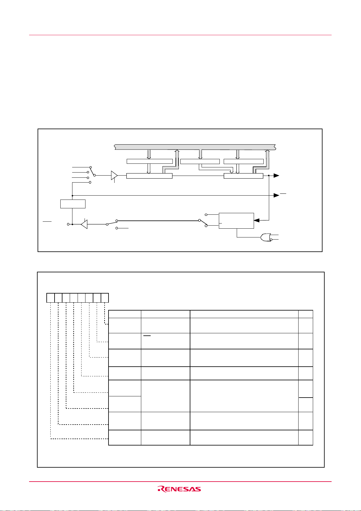
R8C/12 Group
INT2 i
K
T Y C K 1
0
b
b
b
b
b
b
b
b
W
W
W
W
W
W
W
W
12.2 Timer (Timer Y)
12.2 Timer Y
Timer Y is an 8-bit timer with an 8-bit prescaler and has two reload registers-Timer Y Primary and Timer
Y Secondary. Figure 12.11 shows a block diagram of Timer Y. Figures 12.12 to 12.14 show the TYZMR,
PREY, TYSC, TYPR, TYZOC, PUM, and YCSS registers.
The Timer Y has two operation modes as follows:
• Timer mode: The timer counts an internal count source.
• Programmable waveform generation mode: The timer outputs pulses of a given width successively.
Da t a b u s
t o T Y C K
INT2/CNTR1
1
f
f8
I N
fR
G
Polarity
switching
= 0 02
=012
= 1 02
= 1 12
T Y S = 1
T Y O C N T = 0T Y M O D 0 = 1
TYOCNT=1
R e l o a d r e g i s t e r
C o u n t e r
P R E Y r e g i s t e r
P 3 _ 2 b i t i n P 3 r e g i s t e r
T Y S C r e g i s t e r
Reload register
TYOPL=1
T Y O P L = 0
Reload register
Counter
T Y P R r e g i s t e r
Q
Toggle flip-flop
CLR
Q
Timer Y interrupt
C
Write to TYZMR register
T Y M O D 0 b i t = 1
nterrupt
Figure 12.11 Timer Y Block Diagram
Timer Y, Z mode register
7
6
5
4
3
N O T E S :
1 . T h e I R b i t i n t h e I N T 2 I C r e g i s t e r m a y b e s e t t o “ 1 ” ( i n t e r r u p t r e q u e s t e d ) w h e n t h e R 1 E D G b i t i s r e w r i t t e n .
R e f e r t o t h e p a r a g r a p h 1 9 . 2 . 5 “ C h a n g i n g I n t e r r u p t F a c t o r ” i n t h e U s a g e N o t e s R e f e r e n c e B o o k .
2
1
d d r e s
f t e r r e s e
0 8
0
S y m b o lA
T Y Z M R0
B i t n a m e
T Y M O D 0
R 1 E D G
TYWC
T Y S
T Z M O D 0
T Z M O D 1
T Z W C
T Z S
T i m e r Y o p e r a t i o n
m o d e b i t
1
I N T 2 / C N T R
s w i t c h i n g b i t
p o l a r i t y
(1 )
Timer Y write
control bit
Timer Y count
start flag
T i m e r Z o p e r a t i o n
m o d e b i t
T i m e r Z w r i t e
c o n t r o l b i t
T i m e r Z c o u n t
s t a r t f l a g
sA
0
1 6
0 0
t
1 6
F u n c t i o nB i t s y m b o l
0 : T i m e r m o d e
1 : P r o g r a m m a b l e w a v e f o r m g e n e r a t i o n m o d e
0 : R i s i n g e d g e
1 : F a l l i n g e d g e
Function varies depending on the operation
mode
0 : S t o p s c o u n t i n g
1 : S t a r t s c o u n t i n g
b 5 b 4
0 0 : T i m e r m o d e
0 1 : P r o g r a m m a b l e w a v e f o r m g e n e r a t i o n m o d e
1 0 : P r o g r a m m a b l e o n e - s h o t g e n e r a t i o n m o d e
1 1 : P r o g r a m m a b l e w a i t o n e - s h o t g e n e r a t i o n
m o d e
F u n c t i o n v a r i e s d e p e n d i n g o n t h e o p e r a t i o n
m o d e
0 : S t o p s c o u n t i n g
1 : S t a r t s c o u n t i n g
R W
R
R
R
R
R
R
R
R
Figure 12.12 TYZMR Register
Rev.1.20 Jan 27, 2006 page 65 of 181
REJ09B0110-0120
Page 76
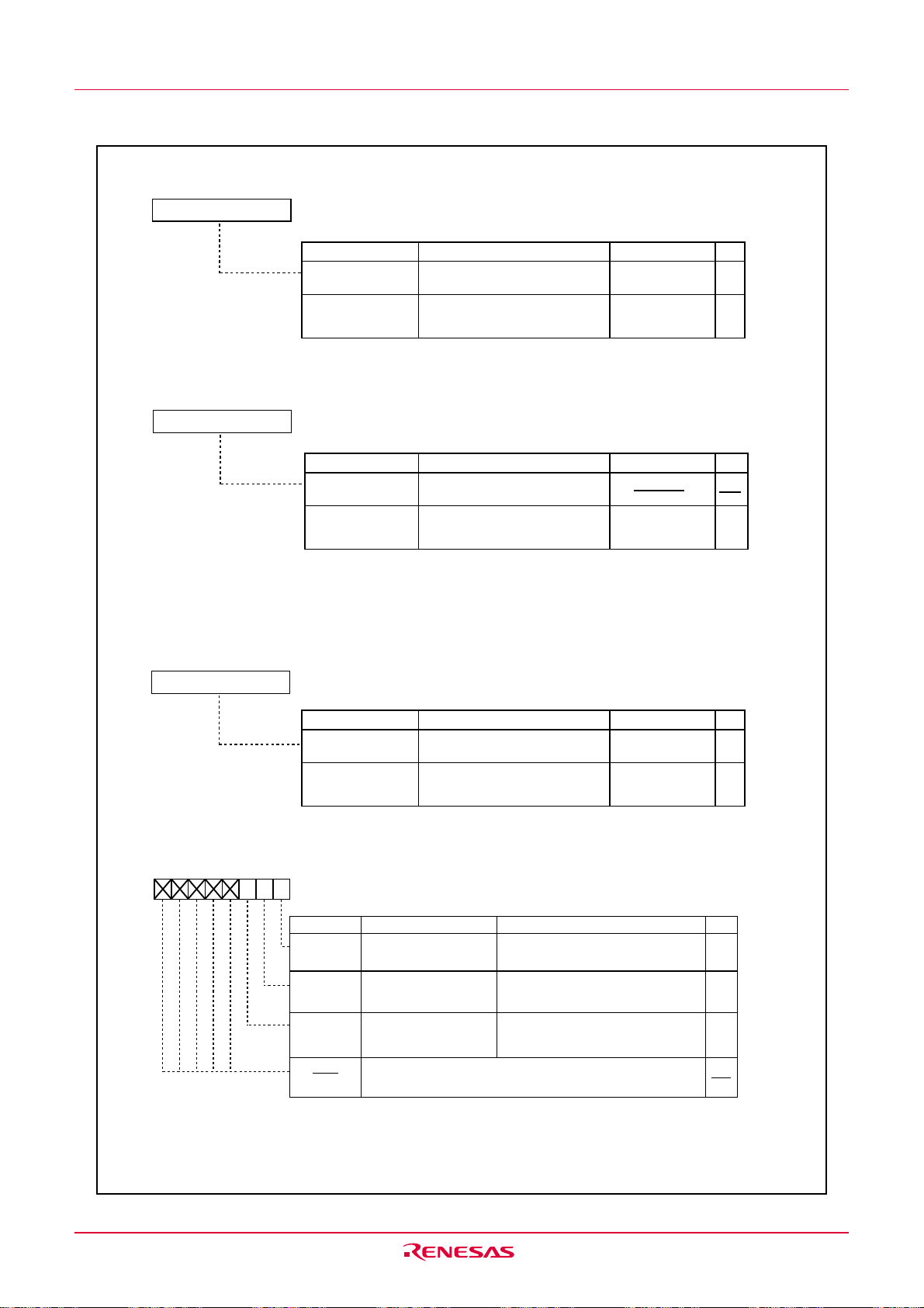
R8C/12 Group
b
b
b
b
b
b
b
b
b
b
b
b
b
b
12.2 Timer (Timer Y)
P r e s c a l e r Y r e g i s t e r
7
T i m e r Y s e c o n d a r y r e g i s t e r
7
0
T i m e r m o d e
P r o g r a m m a b l e
w a v e f o r m g e n e r a t i o n
m o d e
0
T i m e r m o d e
P r o g r a m m a b l e
w a v e f o r m g e n e r a t i o n
m o d e
M o d e
M o d e
d d r e s
f t e r r e s e t
0 8
S y m b o lA
P R E Y0
sA
1
1 6 F
F u n c t i o nS
I n t e r n a l c o u n t s o u r c e o r C N T R 1
i n p u t i s c o u n t e d
I n t e r n a l c o u n t s o u r c e i s c o u n t e d
d d r e s
f t e r r e s e t
0 8
S y m b o lA
T Y S C0
sA
2
1 6 F
F u n c t i o nS
D i s a b l e d
U n d e r f l o w o f P r e s c a l e r Y i s
( 1 )
c o u n t e d
e t t i n g r a n g
e t t i n g r a n g
t o F
0 01
t o F
0 0
t o F
0 01
1 6
F1
6
6
F1
6
F1
6
F1
6
e
6
F1
6
N O T E S :
1 . T h e v a l u e s o f T Y P R r e g i s t e r a n d T Y S C r e g i s t e r a r e r e l o a d e d t o t h e c o u n t e r a l t e r n a t e l y f o r c o u n t i n g .
2 . T h e c o u n t v a l u e c a n b e r e a d o u t b y r e a d i n g t h e T Y P R r e g i s t e r e v e n w h e n t h e s e c o n d a r y p e r i o d i s b e i n g
c o u n t e d .
e
R W
R W
R W
R W
( 2 )
W O
T i m e r Y p r i m a r y r e g i s t e r
7
0
M o d e
T i m e r m o d e
P r o g r a m m a b l e
w a v e f o r m g e n e r a t i o n
m o d e
d d r e s
f t e r r e s e t
0 8
S y m b o lA
T Y P R0
sA
3
1 6 F
F u n c t i o nS
U n d e r f l o w o f P r e s c a l e r Y i s
c o u n t e d
U n d e r f l o w o f P r e s c a l e r Y i s
( 1 )
c o u n t e d
e t t i n g r a n g
t o F
0 0
t o F
0 01
1 6
F1
6
F1
6
F1
N O T E S :
1 . T h e v a l u e s o f T Y P R r e g i s t e r a n d T Y S C r e g i s t e r a r e r e l o a d e d t o t h e c o u n t e r a l t e r n a t e l y f o r c o u n t i n g .
T i m e r Y , Z o u t p u t c o n t r o l r e g i s t e r
7
6
5
4
3
2
1
d d r e s
f t e r r e s e
0 8
0
S y m b o lA
T Y Z O C0
T Z O S
T Y O C N T
T Z O C N T
( b 7 - b 3 )
N O T E S :
1 . T h i s b i t i s s e t t o " 0 " w h e n t h e o u t p u t o f o n e - s h o t w a v e f o r m i s c o m p l e t e d . T h e T Z O S b i t s h o u l d b e s e t t o " 0 " i f t h e
o n e - s h o t w a v e f o r m o u t p u t i s t e r m i n a t e d b y s e t t i n g t h e T Z S b i t i n t h e T Y Z M R t o " 0 " d u r i n g t h e w a v e f o r m o u t p u t .
2 . T h i s b i t i s e n a b l e d o n l y w h e n o p e r a t i n g i n p r o g r a m m a b l e w a v e f o r m g e n e r a t i o n m o d e .
3 . I f e x e c u t i n g a n i n s t r u c t i o n w h i c h c h a n g e s t h i s r e g i s t e r w h e n t h e T Z O S b i t i s “ 1 ” ( d u r i n g t h e c o u n t ) , t h e T Z O S i s
a u t o m a t i c a l l y s e t t o “ 0 ” w h e n t h e c o u n t c o m p l e t e s w h i l e t h e i n s t r u c t i o n i s e x e c u t e d . I f t h i s c a u s e s s o m e p r o b l e m s ,
e x e c u t e a n i n s t r u c t i o n w h i c h c h a n g e s t h i s r e g i s t e r w h e n t h e T Z O S b i t i s “ 0 ” ( o n e s h o t s t o p ) .
( 3 )
sA
A
1 6
Bit name
T i m e r Z o n e - s h o t
( 1 )
s t a r t b i t
T i m e r Y p r o g r a m m a b l e
w a v e f o r m g e n e r a t i o n
o u t p u t s w i t c h i n g b i t
Timer Z programmable
waveform generation
output switching bit
N o t h i n g i s a s s i g n e d .
W h e n w r i t e , s e t t o " 0 " . W h e n r e a d , i t s c o n t e n t i s " 0 " .
0 : S t o p s o n e - s h o t
1 : S t a r t s o n e - s h o t
0 : O u t p u t s p r o g r a m m a b l e w a v e f o r m
1 : O u t p u t s t h e v a l u e o f P 3
( 2 )
0 : O u t p u t s p r o g r a m m a b l e w a v e f o r m
1 : O u t p u t s t h e v a l u e o f P 3
(2)
t
0 0
1 6
FunctionB i t s y m b o l
2
p o r t r e g i s t e r
1
p o r t r e g i s t e r
e
R W
R W
6
R W
6
R W
R W
R W
R W
Figure 12.13 PREY Register, TYSC Register, TYPR Register, and TYZOC Register
Rev.1.20 Jan 27, 2006 page 66 of 181
REJ09B0110-0120
Page 77

R8C/12 Group
b
b
b
b
b
b
b
b
L
r
b7b6b5b4b3b2b1b
0
0
T i m e r Y , Z w a v e f o r m o u t p u t c o n t r o l r e g i s t e r
7
6
12.2 Timer (Timer Y)
5
4
3
2
1
d d r e s
f t e r r e s e
0 8
0
S y m b o lA
P U M0
0000
sA
4
1 6
0 0
t
1 6
Bit symbol
( b 3 - b 0 )
T Y O P
TZOPL
I N O S T G
INOSEG
Bit name
R e s e r v e d b i t
T i m e r Y o u t p u t l e v e l
l a t c h
Timer Z output level
latch
I N T 0 p i n o n e - s h o t t r i g g e
c o n t r o l b i t
INT0 pin one-shot trigger
polarity select bit
(2 )
(Timer Z)
(1)
(Timer Z)
F u n c t i o n
M u s t s e t t o “ 0 ”
F u n c t i o n v a r i e s d e p e n d i n g o n t h e o p e r a t i o n m o d e
Function varies depending on the operation mode
0 : I N T 0 p i n o n e - s h o t t r i g g e r i n v a l i d
1 : I N T 0 p i n o n e - s h o t t r i g g e r v a l i d
0 : Edge trigger at falling edge
1 : Edge trigger at rising edge
N O T E S :
1 . T h e I N O S E G b i t i s v a l i d o n l y w h e n t h e I N T 0 P L b i t i n t h e I N T E N r e g i s t e r i s " 0 " ( o n e - e d g e ) .
2 . T h e I N O S G T b i t m u s t b e s e t t o " 1 " a f t e r t h e I N T 0 E N b i t i n t h e I N T E N r e g i s t e r a n d t h e I N O S E G b i t i n t h e P U M r e g i s t e r
a r e s e t .
Timer count source setting register
d d r e s
f t e r r e s e
0 8
0
S y m b o lA
T C S S0
B i t s y m b o l
T X C K 0
B i t n a m e
Timer X count source
select bit
(1)
T X C K 1
TYCK0
Timer Y count source
select bit
(1)
T Y C K 1
T Z C K 0
Timer Z count source
select bit
(1)
T Z C K 1
( b 7 - b 6 )
R e s e r v e d b i t
NOTES:
1. Avoid switching a count source, while a counter is in progress. Timer counter must be stopped before switching a count
source.
sA
E
1 6 0
b1 b0
t
01
6
0 0 : f1
0 1 : f8
1 0 : f32
1 1 : f2
b3 b2
0 0 : f1
0 1 : f8
1 0 : fRING
1 1 : Selects input from CNTR1 pin
b 5 b 4
0 0 : f1
0 1 : f8
1 0 : Selects Timer Y underflow
1 1 : f
2
Must be set to “0”
F u n c t i o n
RW
RW
RW
RW
R W
RW
RW
R W
R W
RW
R W
R W
RW
R W
Figure 12.14 PUM Register and TCSS Register
Rev.1.20 Jan 27, 2006 page 67 of 181
REJ09B0110-0120
Page 78

R8C/12 Group
12.2 Timer (Timer Y)
12.2.1 Timer Mode
In this mode, the timer counts an internally generated count source (see “Table 12.7 Timer Mode
Specifications”). An external signal input to the CNTR1 pin can be counted. The TYSC register is
unused in timer mode. Figure 12.15 shows the TYZMR and PUM registers in timer mode.
Table 12.7 Timer Mode Specifications
Item Specification
Count source f1, f8, fRING, external signal fed to CNTR1 pin
Count operation • Down-count
• When the timer underflows, it reloads the reload register contents before continuing
counting (When the Timer Y underflows, the contents of the Timer Y primary reload
register is reloaded.)
Divide ratio 1/(n+1)(m+1) n: set value in PREY register, m: set value in TYPR register
Count start condition Write “1” (count start) to TYS bit in TYZMR register
Count stop condition Write “0” (count stop) to TYS bit in TYZMR register
Interrupt request • When Timer Y underflows [Timer Y interrupt]
generation timing
________
INT2/CNTR1 pin function
Programmable I/O port, count source input or INT2 interrupt input
• When the TYCK1 to TYCK0 bits in the TCSS register are set to “00b”, “01b” or “10b”
(Timer Y count source is f1, f8 or fRING), programmable I/O port or INT2 interrupt input
• When the TYCK1 to TYCK0 bits are set to “11b” (Timer Y count source is CNTR
_______
input), count source input (INT2 interrupt input)
Read from timer Count value can be read out by reading TYPR register.
Same applies to PREY register.
Write to timer
(1)
Value written to TYPR register is written to both reload register and counter or written to
only reload register. Selected by program.
Same applies to PREY register.
Select function • Event counter function
When setting TYCK1 to TYCK0 bits to “112”, an external signal fed to CNTR1 pin is
counted.
_______
• INT2/CNTR1 switching bit
Active edge of count source is selected by R1EDG bit.
NOTES:
1. The IR bit in the TYIC register is set to "1" (interrupt requested) if you write to the TYPR or PREY register while both
of the following conditions are met.
Conditions:
• TYWC bit in TYZMR register is "0" (write to reload register and counter simultaneously)
• TYS bit is "1" (count start)
To write to the TYPR or PREY register in the above state, disable interrupts before writing.
_______
_______
1
Rev.1.20 Jan 27, 2006 page 68 of 181
REJ09B0110-0120
Page 79

R8C/12 Group
b
b
b
b
b
b2b
b
T i m e r Y , Z m o d e r e g i s t e r
7
6
12.2 Timer (Timer Y)
5
4
3
1
0
Symbol Address After reset
TYZMR 0080
0
16 0016
TYMOD0
R 1 E D G
T Y W C
TYS
T Z M O D 0
T Z M O D 1
T Z W C
T Z S
Bit name
Timer Y operation
mode bit
INT2/CNTR1 polarity
switching bit
Timer Y write
control bit
Timer Y count
start flag
Timer Z-related bit
(1)
(2)
F u n c t i o nB i t s y m b o l
0 : T i m e r m o d e
0 : Rising edge
1 : Falling edge
0 : Write to reload register and counter
simultaneously
1 : Write to reload register
0 : S t o p s c o u n t i n g
1 : S t a r t s c o u n t i n g
R W
R W
RW
R W
RW
RW
R W
R W
R W
N O T E S :
1 . T h e I R b i t i n t h e I N T 2 I C r e g i s t e r m a y b e s e t t o “ 1 ” ( i n t e r r u p t r e q u e s t e d ) w h e n t h e R 1 E D G b i t i s r e w r i t t e n .
R e f e r t o t h e p a r a g r a p h 1 9 . 2 . 5 “ C h a n g i n g I n t e r r u p t F a c t o r ” i n t h e U s a g e N o t e s R e f e r e n c e B o o k .
2 . W h e n T Y S b i t = 1 ( s t a r t s c o u n t i n g ) , t h e v a l u e s e t i n t h e T Y W C b i t i s v a l i d . I f T Y W C b i t = 0 , t h e t i m e r Y c o u n t v a l u e i s
w r i t t e n t o b o t h r e l o a d r e g i s t e r a n d c o u n t e r . I f T Y W C b i t = 1 , t h e t i m e r Y c o u n t v a l u e i s w r i t t e n t o t h e r e l o a d r e g i s t e r
o n l y .
W h e n T Y S b i t = 0 ( s t o p s c o u n t i n g ) , t h e t i m e r Y c o u n t v a l u e i s w r i t t e n t o b o t h r e l o a d r e g i s t e r a n d c o u n t e r r e g a r d l e s s
o f h o w t h e T Y W C b i t i s s e t .
Timer Y, Z waveform output control register
b7 b6 b5 b4 b3 b2 b1 b0
Symbol Address After reset
PUM 0084
0000
Bit symbol
(b3-b0)
TYOPL
TZOPL
INOSTG
INOSEG
Reserved bit
Timer Y output level
latch
Timer Z-related bits
Bit name
16
0016
Must set to “0”
Invalid in timer mode
Figure 12.15 TYZMR Register and PUM Register in Timer Mode
Function
RW
RW
RW
RW
RW
RW
Rev.1.20 Jan 27, 2006 page 69 of 181
REJ09B0110-0120
Page 80

R8C/12 Group
12.2 Timer (Timer Y)
12.2.2 Programmable Waveform Generation Mode
In this mode, an signal output from the TYOUT pin is inverted each time the counter underflows, while
the values in the TYPR register and TYSC register are counted alternately (see “Table 12.8 Programmable Waveform Generation Mode Specifications”). A counting starts by counting the set value in the
TYPR register. Figure 12.16 shows the TYZMR register in programmable waveform generation mode.
Figure 12.17 shows the operation example.
Table 12.8 Programmable Waveform Generation Mode Specifications
Item Specification
Count source f1, f8, fRING
Count operation • Down count
• When the timer underflows, it reloads the contents of primary reload register and secondary reload register alternately before continuing counting.
(1)
i
.
(2)
.
(3)
.
Output waveform width Primary period : (n+1)(m+1)/f
and period Secondary period : (n+1)(p+1)/fi
Period : (n+1){(m+1)+(p+1)}/fi
n: set value in PREY register, m: set value in TYPR register, p: set value in TYSC register
fi : Count source frequency
Count start condition Write “1” (count start) to TYS bit in TYZMR register
Count stop condition Write “0” (count stop) to TYS bit in TYZMR register
Interrupt request generation timing
_____
INT2/CNTR1 pin functions Pulse output
In half of count source, after timer Y underflows during secondary period (at the same
time as the CNTR, output change) [Timer Y interrupt]
Use timer mode when using this pin as a programmable I/O port.
Read from timer Count value can be read out by reading TYPR register.
Same applies to PREY register
Write to timer
Value written to TYPR register is written to only reload register.
Same applies to TYSC register and PREY register
Select function • Output level latch select function
The output level during primary and secondary periods is selected by the TYOPL bit.
• Programmable waveform generation output switching function
When the TYOCNT bit in the TYZOC register is set to “0”, the output from TYOUT is
inverted synchronously when Timer Y underflows during the secondary period. And
when set to “1”, a value in the P3_2 bit is output from TYOUT synchronously when Timer
Y underflows during the secondary period
NOTES:
1. Even when counting the secondary period, read out the TYPR register.
2. The set value in the TYPR register and TYSC register are made effective by writing a value to the TYPR register. The
written values are reflected to the waveform output from the next primary period after writing to the TYPR register.
3. The TYOCNTbit is enabled in the following timings
• When count starts
• When Timer Y interrupt request is generated
Therefore, pulse is output from the next primary period depending on the setting value of the TYOCNT bit
Rev.1.20 Jan 27, 2006 page 70 of 181
REJ09B0110-0120
Page 81

R8C/12 Group
b
b
b5b
b
b
b
b
12.2 Timer (Timer Y)
T i m e r Y , Z m o d e r e g i s t e r
7
6
4
3
2
1
1
d d r e s
f t e r r e s e
0 8
0
S y m b o lA
T Y Z M R0
1
B i t n a m e
T Y M O D 0
R 1 E D G
T Y W C
TYS
TZMOD0
T i m e r Y o p e r a t i o n
m o d e b i t
I N T 2 / C N T R
s w i t c h i n g b i t
1
p o l a r i t y
(1 , 3 )
Timer Y write
control bit
T i m e r Y c o u n t
s t a r t f l a g
T i m e r Z - r e l a t e d b i t
sA
0
1 6
0 0
t
1 6
FunctionBit symbol
1 : P r o g r a m m a b l e w a v e f o r m g e n e r a t i o n m o d e
D i s a b l e d i n p r o g r a m m a b l e w a v e f o r m
g e n e r a t i o n m o d e
Set to “1” in programmable waveform generation
(2)
.
mode
0 : Stops counting
1 : Starts counting
TZMOD1
TZWC
TZS
NOTES:
1. The IR bit in the INT2IC register may be set to “1” (interrupt requested) when the R1EDG bit is rewritten.
Refer to the paragraph 19.2.5 “Changing Interrupt Factor” in the Usage Notes Reference Book.
2 . W h e n T Y S b i t = 1 ( s t a r t s c o u n t i n g ) , t h e t i m e r Y c o u n t v a l u e i s w r i t t e n t o t h e r e l o a d r e g i s t e r o n l y .
W h e n T Y S b i t = 0 ( s t o p s c o u n t i n g ) , t h e t i m e r Y c o u n t v a l u e i s w r i t t e n t o b o t h r e l o a d r e g i s t e r a n d c o u n t e r .
3 . T h e I N T 2 i n t e r r u p t r e q u e s t i s n o t g e n e r a t e d w h e n t h e T Y M O D 0 b i t i s s e t t o “ 1 ” ( p r o g r a m m a b l e w a v e f o r m
g e n e r a t i o n m o d e ) .
RW
RW
RW
RW
RW
RW
RW
RW
RW
Timer Y, Z waveform output control register
b7 b6 b5 b4 b3 b2 b1 b0
Symbol Address After reset
PUM 0084
0000
Bit symbol
(b3-b0)
TYOPL
TZOPL
INOSTG
INOSEG
Timer Y output level
latch
Timer Z-related bits
Bit name
Reserved bit
16
0016
Function
Must set to “0”
0 : Outputs "H" for primary period
Outputs "L" for secondary period
Outputs "L" when the timer is stopped
1 : Outputs "L" for primary period
Outputs "H" for secondary period
Outputs "H" when the timer is stopped
RW
RW
RW
RW
RW
RW
Figure 12.16 TYZMR Register and PUM Register in Programmable Waveform Generation Mode
Rev.1.20 Jan 27, 2006 page 71 of 181
REJ09B0110-0120
Page 82

R8C/12 Group
12.2 Timer (Timer Y)
Set to "1" by program
TYS bit in TYZMR
register
Count source
Prescaler Y
underflow signal
Contents of Timer Y
IR bit in TYIC
register
TYOPL bit in PUM
register
"1"
"0"
"1"
"0"
"1"
"0"
Count starts
Set to "0" by program
01
Timer Y
secondary
reloads
16
00
16
02
16
01
16
Timer Y
primary
reloads
00
16
Set to "0" when interrupt request is
accepted, or set by program
01
16
00
16
02
16
CNTR1 pin output
"H"
Waveform output
started
Waveform output
inverted
Waveform output
inverted
"L"
Primary period
Conditions: PREY=0116, TYPR=01
16,
TYSC=02
Secondary period
16
Primary period
TYZOC register TYOCNT bit = 0
Figure 12.17 Timer Y Operation Example in Programmable Waveform Generation Mode
Rev.1.20 Jan 27, 2006 page 72 of 181
REJ09B0110-0120
Page 83

R8C/12 Group
8
2
T
r
r
r
L
t
t
K
b
b
b
b
b
b
b1b
W
W
W
W
W
W
W
W
12.3 Timer (Timer Z)
12.3 Timer Z
Timer Z is an 8-bit timer with an 8-bit prescaler and has two reload registers-Timer Z Primary and Timer
Z Secondary. Figure 12.18 shows a block diagram of Timer Z. Figures 12.19 to 12.21 show the TYZMR,
PREZ, TZSC, TZPR, TYZOC, PUM, and TCSS registers.
Timer Z has the following four operation modes.
• Timer mode: The timer counts an internal count source or Timer Y underflow.
• Programmable waveform generation mode: The timer outputs pulses of a given width successively.
• Programmable one-shot generation mode: The timer outputs one-shot pulse.
• Programmable wait one-shot generation mode: The timer outputs delayed one-shot pulse.
Data bus
T Z C K 1 t o T Z C K 0
f1
f
imer Y underflow
INT0
TZMOD1 to TZMOD0= 012, 102, 11
T Z
O U
= 1 02
= 1 12
f
= 0 0
= 0 12
2
D i g i t a l
f i l t e r
2
TZOCNT=0
TZOCNT=1
R e l o a d r e g i s t e
P R E Z r e g i s t e r
T Z S
I n p u t p o l a r i t y s e l e c t e d t o b e
o n e e d g e o r b o t h e d g e s
I N T 0 P
INT0EN
P 3 _ 1 b i t i n P 3 r e g i s t e r
TZMOD1 to TZMOD0= 10
Reload registe
P o l a r i t y
s e l e c t
INOSEG
TZOPL=1
T Z O P L = 0
T Z S C r e g i s t e r
2
,
Q
Q
Reload registe
11
2
T Z O S
Toggle flip-flop
CLR
Counter C o u n t e r
T Z P R r e g i s t e r
C
T i m e r Z i n t e r r u p
I N T 0 i n t e r r u p
W r i t e t o T Y Z M R r e g i s t e r
T Z M O D 1 t o T Z M O D 0 b i t s = 0 1
2
, 1 02, 1 1
2
Figure 12.18 Timer Z Block Diagram
T i m e r Y , Z m o d e r e g i s t e r
7
6
5
4
3
2
N O T E S :
1 . T h e I R b i t i n t h e I N T 2 I C r e g i s t e r m a y b e s e t t o “ 1 ” ( i n t e r r u p t r e q u e s t e d ) w h e n t h e R 1 E D G b i t i s r e w r i t t e n .
R e f e r t o t h e p a r a g r a p h 1 9 . 2 . 5 “ C h a n g i n g I n t e r r u p t F a c t o r ” i n t h e U s a g e N o t e s R e f e r e n c e B o o k .
d d r e s
f t e r r e s e
0 8
0
S y m b o lA
T Y Z M R0
Bit name
T Y M O D 0
R 1 E D G
T Y W C
TYS
TZMOD0
T Z M O D 1
T Z W C
T Z S
T i m e r Y o p e r a t i o n
m o d e b i t
INT2/CNTR
1
switching bit
T i m e r Y w r i t e
c o n t r o l b i t
T i m e r Y c o u n t
s t a r t f l a g
Timer Z operation
mode bit
T i m e r Z w r i t e
c o n t r o l b i t
T i m e r Z c o u n t
s t a r t f l a g
sA
0
1 6
0 : T i m e r m o d e
1 : P r o g r a m m a b l e w a v e f o r m g e n e r a t i o n m o d e
polarity
(1)
0 : R i s i n g e d g e
1 : F a l l i n g e d g e
F u n c t i o n v a r i e s d e p e n d i n g o n t h e o p e r a t i o n
m o d e
0 : S t o p s c o u n t i n g
1 : S t a r t s c o u n t i n g
b 5 b 4
0 0 : T i m e r m o d e
0 1 : P r o g r a m m a b l e w a v e f o r m g e n e r a t i o n m o d e
1 0 : P r o g r a m m a b l e o n e - s h o t g e n e r a t i o n m o d e
1 1 : P r o g r a m m a b l e w a i t o n e - s h o t g e n e r a t i o n
F u n c t i o n v a r i e s d e p e n d i n g o n t h e o p e r a t i o n
m o d e
0 : S t o p s c o u n t i n g
1 : S t a r t s c o u n t i n g
m o d e
0 0
t
1 6
FunctionB i t s y m b o l
R W
R
R
R
R
R
R
R
R
Figure 12.19 TYZMR Register
Rev.1.20 Jan 27, 2006 page 73 of 181
REJ09B0110-0120
Page 84

R8C/12 Group
b
b
b
b
b
b
b
b
b
b
b3b
b
b
12.3 Timer (Timer Z)
P r e s c a l e r Z r e g i s t e r
7
M o d e
T i m e r m o d e
P r o g r a m m a b l e
w a v e f o r m
g e n e r a t i o n m o d e
P r o g r a m m a b l e
o n e - s h o t
g e n e r a t i o n m o d e
P r o g r a m m a b l e w a i t
o n e - s h o t g e n e r a t i o n
m o d e
T i m e r Z S e c o n d a r y r e g i s t e r
7
M o d e
Timer mode
P r o g r a m m a b l e
w a v e f o r m
g e n e r a t i o n m o d e
P r o g r a m m a b l e
o n e - s h o t
g e n e r a t i o n m o d e
P r o g r a m m a b l e w a i t
o n e - s h o t g e n e r a t i o n
N O T E S :
1 . E a c h v a l u e i n t h e T Z P R r e g i s t e r a n d T Z S C r e g i s t e r i s r e l o a d e d t o t h e c o u n t e r a l t e r n a t e l y f o r c o u n t i n g .
2 . T h e c o u n t v a l u e c a n b e r e a d o u t b y r e a d i n g t h e T Z S C r e g i s t e r e v e n w h e n t h e s e c o n d a r y p e r i o d i s b e i n g
c o u n t e d .
Timer Z Primary register
7
m o d e
d d r e s
f t e r r e s e t
0 8
S y m b o lA
0
P R E Z0
sA
5
1 6
Function Setting range
I n t e r n a l c o u n t s o u r c e o r T i m e r Y
u n d e r f l o w i s c o u n t e d
I n t e r n a l c o u n t s o u r c e o r T i m e r Y
u n d e r f l o w i s c o u n t e d
Internal count source or Timer Y
underflow is counted 0 0
I n t e r n a l c o u n t s o u r c e o r T i m e r Y
u n d e r f l o w i s c o u n t e d
d d r e s
f t e r r e s e t
0 8
S y m b o lA
0
T Z S C0
sA
6
1 6
Function Setting range
I n v a l i d
U n d e r f l o w o f
P r e s c a l e r Z i s c o u n t e d
( 1 )
Invalid
U n d e r f l o w o f P r e s c a l e r Z i s
c o u n t e d
( O n e - s h o t w i d t h i s c o u n t e d )
Symbol Address After reset
0
TZPR 0087
16
F F
1 6
0 0
1 6
t o F F
1 6
0 0
1 6
t o F F
1 6
1 6
t o F F
1 6
00
16
to FF
16
F F
1 6
0 0
1 6
t o F F
1 6
00
16
to FF
16
FF
16
R W
R W
R W
RW
R W
RW
( 2 )
W O
WO
Mode
T i m e r m o d e
P r o g r a m m a b l e
w a v e f o r m
g e n e r a t i o n m o d e
P r o g r a m m a b l e
o n e - s h o t
g e n e r a t i o n m o d e
P r o g r a m m a b l e w a i t
o n e - s h o t g e n e r a t i o n
N O T E S :
1 . E a c h v a l u e i n t h e T Z P R r e g i s t e r a n d T Z S C r e g i s t e r i s r e l o a d e d t o t h e c o u n t e r a l t e r n a t e l y f o r c o u n t i n g .
T i m e r Y , Z o u t p u t c o n t r o l r e g i s t e r
7
6
5
4
m o d e
2
1
0
Symbol Address After reset
TYZOC 008A
U n d e r f l o w o f P r e s c a l e r Z i s
c o u n t e d
Underflow of
Prescaler Z is counted
Underflow of Prescaler Z is
counted
(One-shot width is counted)
U n d e r f l o w o f P r e s c a l e r Z i s
c o u n t e d
( W a i t p e r i o d i s c o u n t e d )
( 3 )
Bit name
( b 7 - b 3 )
Timer Z one-shot
(1)
start bit
Timer Y programmable
waveform generation
output switching bit
T i m e r Z p r o g r a m m a b l e
w a v e f o r m g e n e r a t i o n
o u t p u t s w i t c h i n g b i t
Nothing is assigned.
When write, set to "0". When read, its content is "0".
T Z O S
T Y O C N T
T Z O C N T
N O T E S :
1 . T h i s b i t i s s e t t o " 0 " w h e n t h e o u t p u t o f o n e - s h o t w a v e f o r m i s c o m p l e t e d . T h e T Z O S b i t s h o u l d b e s e t t o " 0 " i f t h e
o n e - s h o t w a v e f o r m o u t p u t i s t e r m i n a t e d b y s e t t i n g t h e T Z S b i t i n t h e T Y Z M R t o " 0 " d u r i n g t h e w a v e f o r m o u t p u t .
2 . T h i s b i t i s e n a b l e d o n l y w h e n o p e r a t i n g i n p r o g r a m m a b l e w a v e f o r m g e n e r a t i o n m o d e .
3 . I f e x e c u t i n g a n i n s t r u c t i o n w h i c h c h a n g e s t h i s r e g i s t e r w h e n t h e T Z O S b i t i s “ 1 ” ( d u r i n g t h e c o u n t ) , t h e T Z O S i s
a u t o m a t i c a l l y s e t t o “ 0 ” w h e n t h e c o u n t c o m p l e t e s w h i l e t h e i n s t r u c t i o n i s e x e c u t e d . I f t h i s c a u s e s s o m e p r o b l e m s ,
e x e c u t e a n i n s t r u c t i o n w h i c h c h a n g e s t h i s r e g i s t e r w h e n t h e T Z O S b i t i s “ 0 ” ( o n e s h o t s t o p ) .
Function Setting range
0 0
(1)
0 0
0 0
00
16
00
16
FunctionB i t s y m b o l
0 : Stops one-shot
1 : Starts one-shot
0 : O u t p u t s p r o g r a m m a b l e w a v e f o r m
1 : O u t p u t s t h e v a l u e o f P 3
(2)
0 : O u t p u t s p r o g r a m m a b l e w a v e f o r m
1 : O u t p u t s t h e v a l u e o f P 3
( 2 )
1 6
t o F F
1 6
t o F F
1 6
t o F F
16
to FF
2
p o r t r e g i s t e r
1
p o r t r e g i s t e r
R W
1 6
R W
RW
1 6
1 6
RW
RW
16
RW
RW
R W
RW
Figure 12.20 PREZ Register, TZSC Register, TZPR Register, and TYZOC Register
Rev.1.20 Jan 27, 2006 page 74 of 181
REJ09B0110-0120
Page 85

R8C/12 Group
b
b
b
b
b3b2b
b
L
r
b7b6b5b4b3b2b1b
0
0
T i m e r Y , Z w a v e f o r m o u t p u t c o n t r o l r e g i s t e r
7
6
5
4
1
d d r e s
f t e r r e s e
0 8
0
S y m b o lA
P U M0
0000
sA
4
1 6
0 0
12.3 Timer (Timer Z)
t
1 6
B i t s y m b o l
( b 3 - b 0 )
T Y O P
T Z O P L
INOSTG
I N O S E G
B i t n a m e
Reserved bit
Timer Y output level
latch
Timer Z output level
latch
INT0 pin one-shot trigge
control bit
INT0 pin one-shot trigger
polarity select bit
(2)
( T i m e r Z )
(1)
(Timer Z)
F u n c t i o n
M u s t s e t t o “ 0 ”
F u n c t i o n v a r i e s d e p e n d i n g o n t h e o p e r a t i o n m o d e
F u n c t i o n v a r i e s d e p e n d i n g o n t h e o p e r a t i o n m o d e
0 : I N T 0 p i n o n e - s h o t t r i g g e r i n v a l i d
1 : I N T 0 p i n o n e - s h o t t r i g g e r v a l i d
0 : Edge trigger at falling edge
1 : Edge trigger at rising edge
NOTES:
1. The INOSEG bit is valid only when the INT0PL bit in the INTEN register is "0" (one-edge).
2. The INOSGT bit must be set to "1" after the INT0EN bit in the INTEN register and the INOSEG bit in the PUM register
are set.
T i m e r c o u n t s o u r c e s e t t i n g r e g i s t e r
0
Symbol Address After reset
TCSS 008E
B i t s y m b o l
T X C K 0
B i t n a m e
Timer X count source
select bit
(1)
TXCK1
T Y C K 0
T i m e r Y c o u n t s o u r c e
s e l e c t b i t
(1 )
T Y C K 1
TZCK0
Timer Z count source
select bit
(1)
T Z C K 1
Reserved bit
s o u r c e
N O T E S :
( b 7 - b 6 )
1 . A v o i d s w i t c h i n g a c o u n t s o u r c e , w h i l e a c o u n t e r i s i n p r o g r e s s . T i m e r c o u n t e r m u s t b e s t o p p e d b e f o r e s w i t c h i n g a c o u n t
.
16
00
16
F u n c t i o n
b 1 b 0
0 0 : f
1
0 1 : f
8
1 0 : f
3 2
1 1 : f
2
b3 b2
0 0 : f
1
0 1 : f
8
1 0 : f
R I N G
1 1 : S e l e c t s i n p u t f r o m C N T R1 p i n
b 5 b 4
0 0 : f
1
0 1 : f
8
1 0 : Selects Timer Y underflow
1 1 : f
2
Must be set to “0”
R W
R W
RW
R W
R W
R W
R W
RW
R W
RW
R W
RW
R W
R W
Figure 12.21 PUM Register and TCSS Register
Rev.1.20 Jan 27, 2006 page 75 of 181
REJ09B0110-0120
Page 86

R8C/12 Group
12.3 Timer (Timer Z)
12.3.1 Timer Mode
In this mode, the timer counts an internally generated count source or Timer Y underflow (see “Table
12.9 Timer Mode Specifications”). The Timer Z secondary is unused in timer mode. Figure 12.22
shows the TYZMR register and PUM register in timer mode.
Table 12.9 Timer Mode Specifications
Item Specification
Count source f1, f2, f8, Timer Y underflow
Count operation • Down-count
• When the timer underflows, it reloads the reload register contents before continuing
counting (When the Timer Z underflows, the contents of the Timer Z primary reload
register is reloaded.)
Divide ratio 1/(n+1)(m+1) n: set value in PREZ register, m: set value in TZPR register
Count start condition Write “1” (count start) to TZS bit in TYZMR register
Count stop condition Write “0” (count stop) to TZS bit in TYZMR register
Interrupt request • When Timer Z underflows [Timer Z interrupt]
generation timing
TZOUT pin function Programmable I/O port
INT0 pin function
Read from timer Count value can be read out by reading TZPR register.
Write to timer
NOTES:
1. The IR bit in the TZIC register is set to "1" (interrupt requested) if you write to the TZPR or PREZ register while both
of the following conditions are met.
<Conditions>
• TZWC bit in TYZMR register is set to "0" (write to reload register and counter simultaneously)
• TZS bit in TYZMR register is set to "1" (count start)
To write to the TZPR or PREZ register in the above state, disable interrupts before the writing.
(1)
Programmable I/O port, or INT0 interrupt input
Same applies to PREZ register.
Value written to TZPR register is written to both reload register and counter or written to
reload register only. Selected by program.
Same applies to PREZ register.
_______
Rev.1.20 Jan 27, 2006 page 76 of 181
REJ09B0110-0120
Page 87

R8C/12 Group
b7b
b
b
b
b
b
b
T i m e r Y , Z m o d e r e g i s t e r
6
5
4
3
0
0
12.3 Timer (Timer Z)
2
1
0
Symbol Address After reset
TYZMR 0080
16
00
16
F u n c t i o nBit symbol
T Y M O D 0
Bit name
T i m e r Y - r e l a t e d b i t
R 1 E D G
TYWC
TYS
b 5 b 4
0 0 : T i m e r m o d e
TZMOD0
T i m e r Z o p e r a t i o n
m o d e b i t
TZMOD1
T Z W C
T Z S
T i m e r Z w r i t e
c o n t r o l b i t
(1 )
T i m e r Z c o u n t
s t a r t f l a g
0 : Write to reload register and counter
1 : Write to reload register only
0 : S t o p s c o u n t i n g
1 : S t a r t s c o u n t i n g
NOTES:
1. When TZS bit=1 (starts counting), the value set in the TZWC bit is valid. If TZWC bit=0, the timer Z count value is
written to both reload register and counter. If TZWC bit=1, the timer Z count value is written to the reload register
only.
When TZS bit=0 (stops counting), the timer Z count value is written to both reload register and counter regardless of
how the TZWC bit is set.
R W
R W
R W
RW
R W
R W
R W
R W
R W
Timer Y, Z waveform output control register
b7 b6 b5 b4 b3 b2 b1 b0
000
Figure 12.22
TYZMR Register and PUM Register in Timer Mode
Symbol Address After reset
PUM 0084
0000
Bit symbol
(b3-b0)
TYOPL
TZOPL
INOSTG
INOSEG
Reserved bit
Timer Y-related bit
Timer Z output level
latch
INT0 pin one-shot
trigger control bit
INT0 pin one-shot trigger
polarity select bit
Bit name
16
0016
Must set to “0”
Must set to “0” in timer mode
Must set to “0” in timer mode
Must set to “0” in timer mode
Function
RW
RW
RW
RW
RW
RW
Rev.1.20 Jan 27, 2006 page 77 of 181
REJ09B0110-0120
Page 88

R8C/12 Group
12.3 Timer (Timer Z)
12.3.2 Programmable Waveform Generation Mode
In this mode, an signal output from the TZOUT pin is inverted each time the counter underflows, while
the values in the TZPR register and TZSC register are counted alternately (see “Table 12.10 Programmable Waveform Generation Mode Specifications”). A counting starts by counting the value set in the
TZPR register. Figure 12.23 shows TYZMR and PUM registers in this mode. The Timer Z operates in
the same way as the Timer Y in this mode. See Figure 12.17 (Timer Y operation example in programmable waveform generation mode ).
Table 12.10 Programmable Waveform Generation Mode Specifications
Item Specification
Count source f1, f2, f8, Timer Y underflow
Count operation • Down-count
• When the timer underflows, it reloads the contents of primary reload register and secondary reload register alternately before continuing counting.
Output waveform width Primary period : (n+1)(m+1)/f
and period Secondary period : (n+1)(p+1)/fi
Period : (n+1){(m+1)+(p+1)}/fi
fi : Count source frequency
n: Set value in PREZ register, m: Set value in TZPR register, p: Set value in TZSC register
Count start condition Write “1” (count start) to the TZS bit in the TYZMR register
Count stop condition Write “0” (count stop) to the TZS bit in the TYZMR register
Interrupt request generation timing
In half of count source, after timer Z underflows during secondary period (at the same
time as the TZout output change) [Timer Z interrupt]
OUT pin function Pulse output
TZ
_____
INT0 pin functions
Use timer mode when using this pin as a programmable I/O port.
Programmable I/O port, or INT0 interrupt input
Read from timer Count value can be read out by reading TZPR register.
Same applies to PREZ register
Write to timer
Value written to TZPR register is written to reload register only.
Same applies to TZSC register and PREZ register
Select function • Output level latch select function
The output level during primary and secondary periods is selected by the TZOPL bit.
• Programmable waveform generation output switching function
The output from TZOUT is inverted synchronously when Timer Z underflows by setting
the TZOCNT bit in the TYZOC register to “0”. A value in the P3_1 bit is output from the
TZOUT by setting to “1”
(3)
NOTES:
1. Even when counting the secondary period, read out the TZPR register.
2. The set value in the TZPR register and TZSC register are made effective by writing a value to the TZPR register. The
set values are reflected to the waveform output beginning with the next primary period after writing to the Timer Z
primary register.
3. The TZOCNTbit is enabled in the following timings
• When count starts
• When Timer Z interrupt request is generated
Therefore, pulse is output from the next primary period depending on the setting value of the TZOCNT bit.
_______
.
(2)
i
.
(3)
.
Rev.1.20 Jan 27, 2006 page 78 of 181
REJ09B0110-0120
Page 89

R8C/12 Group
b
b6b
b
b
b
b
b
L
00000
0
b
b
b5b
b
b
b
b
12.3 Timer (Timer Z)
T i m e r Y , Z m o d e r e g i s t e r
7
6
4
11
0
3
2
1
d d r e s
f t e r r e s e
0 8
0
S y m b o lA
T Y Z M R0
B i t n a m e
T Y M O D 0
T i m e r Y - r e l a t e d b i t
sA
0
1 6
0 0
t
1 6
FunctionB i t s y m b o l
R 1 E D G
T Y W C
T Y S
b5 b4
0 1 : Programmable waveform generation mode
TZMOD0
T i m e r Z o p e r a t i o n
m o d e b i t
TZMOD1
NOTES:
T Z W C
TZS
Timer Z write
control bit
Timer Z count
start flag
Set to "1" in programmable waveform generation
(1)
mode
0 : Stops counting
1 : Starts counting
1. When TZS bit=1(starts counting), the timer Y count vaue is written to the reload register only.
When TZS bit=0(stops counting), the timer Y count value is written to both reload register and counter.
R W
R W
R W
R W
R W
R W
R W
R W
RW
Timer Y, Z waveform output control register
7
5
4
Figure 12.23
3
TYZMR Register and PUM Register in
2
1
0
Symbol Address After reset
PUM 0084
Bit symbol
(b3-b0)
TYOP
TZOPL
INOSTG
INOSEG
Reserved bit
T i m e r Y - r e l a t e d b i t
T i m e r Z o u t p u t l e v e l
l a t c h
I N T 0 p i n o n e - s h o t
t r i g g e r c o n t r o l b i t
I N T 0 p i n o n e - s h o t
t r i g g e r p o l a r i t y s e l e c t b i t
B i t n a m e
16
00
16
F u n c t i o n
Must set to “0”
0 : Outputs "H" for primary period
Outputs "L" for secondary period
Outputs "L" when the timer is stopped
1 : Outputs "L" for primary period
Outputs "H" for secondary period
Outputs "H" when the timer is stopped
Must set to “0” in programmable waveform
generation mode
Must set to “0” in programmable waveform
generation mode
Programmable Waveform Generation Mode
R W
R W
R W
R W
RW
R W
Rev.1.20 Jan 27, 2006 page 79 of 181
REJ09B0110-0120
Page 90

R8C/12 Group
12.3 Timer (Timer Z)
12.3.3 Programmable One-shot Generation Mode
In this mode, upon program command or external trigger input (input to the INT0 pin), the microcomputer outputs the one-shot pulse from the TZOUT pin (see “Table 12.11 Programmable One-shot
Generation Mode Specifications”). When a trigger occurs, the timer starts operating from the point
only once for a given period equal to the set value in the TZPR register. The TZSC is unused in this
mode. Figure 12.24 shows the TYZMR register and PUM register in this mode. Figure 12.25 shows
an operation example in this mode.
Table 12.11 Programmable One-shot Generation Mode Specifications
Item Specification
Count source f1, f2, f8, Timer Y underflow
Count operation • Downcounts set value in TZPR register
• When the timer underflows, it reloads the contents of reload register before completing
counting.
• When a count stops, the timer reloads the contents of the reload register before it stops.
Divide ratio (n+1)(m+1)/fi
n: set value in PREZ register, m: set value in TZPR register
Count start condition • Set TZOS bit in TYZOC register to “1” (start one-shot)
• Input active trigger to INT0 pin
(2)
Count stop condition • When reloading is completed after count value was set to "0016"
• When TZS bit in TYZMR register is set to “0” (stop counting)
• When TZOS bit in TYZOC register is set to “0” (stop one-shot)
Interrupt request generation timing
In half cycles of count source, after the timer underflows (at the same time as the TZout
output ends) [Timer Z interrupt]
OUT pin function Pulse output
TZ
_______
Use timer mode when using this pin as a programmable I/O port.
INT0 pin function Programmable I/O port, external interrupt input pin, or external trigger input pin
• When the INOSTG bit in the PUM register is set to “0” (INT0 one-shot trigger disabled)
_______
Programmable I/O port or INT0 interrupt input
• When the INOSTG bit in the PUM register is set to “1” (INT0 one-shot trigger enabled)
_______
external trigger (INT0 interrupt input)
Read from timer Count value can be read out by reading TZPR register.
Same applies to PREZ register.
Write to timer
Value written to TZPR register is written to reload register only
Same applies to PREZ register.
Select function • Output level latch select function
Output level for one-shot pulse waveform is selected by TZOPL bit.
_______
• INT0 pin one-shot trigger control function and polarity select function
_______
Trigger input from INT0 pin can be set to active or inactive by INOSTG bit. Also, an
active trigger's polarity can be selected by INOSEG bit.
NOTES:
1. The TZS bit in the TYZMR register must be set to "1" (start counting).
2. The TZS bit must be set to "1" (start counting), the INT0EN bit in the INTEN register to "1" (enabling INT0 input), and
the INOSTG bit in the PUM register to "1" (enabling INT0 one-shot trigger).
_______
_______
Although the trigger input during counting cannot be acknowledged, the INT0 interrupt request is generated.
3. The set values are reflected beginning with the next one-shot pulse after writing to the TZPR register.
(1)
_______
_______
(3)
.
_______
Rev.1.20 Jan 27, 2006 page 80 of 181
REJ09B0110-0120
Page 91

R8C/12 Group
b
b
b
b
b
b
b
b
L
r
000
0
b
b
b
b
b
b
b
b
T i m e r Y , Z m o d e r e g i s t e r
7
6
12.3 Timer (Timer Z)
5
4
3
01
1
0
2
1
Symbol Address After reset
TYZMR 0080
16
00
16
FunctionB i t s y m b o l
T Y M O D 0
B i t n a m e
T i m e r Y - r e l a t e d b i t
R 1 E D G
TYWC
T Y S
b5 b4
1 0 : P r o g r a m m a b l e o n e - s h o t g e n e r a t i o n m o d e
T Z M O D 0
T i m e r Z o p e r a t i o n
m o d e b i t
T Z M O D 1
NOTES:
T Z W C
T Z S
T i m e r Z w r i t e
c o n t r o l b i t
Timer Z count
start flag
Set to "1" in programmable one-shot generation
(1)
mode
0 : S t o p s c o u n t i n g
1 : S t a r t s c o u n t i n g
1. When the TZS bit is set to “1”(count starts), the count value is written to the reload register only.
When the TZS bit is set to “0”(count stops), the count value is written to both the reload register and counter.
T i m e r Y , Z w a v e f o r m o u t p u t c o n t r o l r e g i s t e r
7
6
5
4
3
2
1
d d r e s
f t e r r e s e
0 8
0
S y m b o lA
P U M0
sA
4
1 6
0 0
t
1 6
R W
R W
R W
R W
R W
R W
R W
RW
R W
B i t s y m b o l
( b 3 - b 0 )
T Y O P
T Z O P L
B i t n a m e
R e s e r v e d b i t
T i m e r Y - r e l a t e d b i t
T i m e r Z o u t p u t l e v e l
l a t c h
Function
M u s t s e t t o “ 0 ”
0 : Outputs "H" level one-shot pulse.
Outputs "L" when the timer is stopped.
1 : Outputs "L" level one-shot pulse
Outputs "H" when the timer is stopped.
I N O S T G
I N O S E G
I N T 0 p i n o n e - s h o t t r i g g e
c o n t r o l b i t
I N T 0 p i n o n e - s h o t t r i g g e r
p o l a r i t y s e l e c t b i t
(2 )
(1 )
0 : INT0 pin one-shot trigger disabled
1 : INT0 pin one-shot trigger enabled
0 : Edge trigger at falling edge
1 : Edge trigger at rising edge
(2)
N O T E S :
1 . T h e I N O S E G b i t i s v a l i d o n l y w h e n t h e I N T 0 P L b i t i n t h e I N T E N r e g i s t e r i s s e t t o " 0 " ( o n e - e d g e ) .
2 . T h e I N O S G T b i t m u s t b e s e t t o “ 1 ” a f t e r t h e I N T 0 E N b i t i n t h e I N T E N r e g i s t e r a n d t h e I N O S E G b i t i n t h e P U M r e g i s t e r a r e s e t .
W h e n s e t t i n g t h e I N O S T G b i t t o " 1 " ( I N T 0 p i n o n e - s h o t t r i g g e r e n a b l e d ) , t h e I N T 0 F 0 a n d I N T 0 F 1 b i t s i n t h e I N T 0 F r e g i s t e r
m u s t b e s e t .
T h e I N O S T G b i t m u s t b e s e t t o “ 0 ” ( I N T 0 p i n o n e - s h o t t r i g g e r d i s a b l e d ) a f t e r t h e T Z S b i t i n t h e T Y Z M R r e g i s t e r i s s e t t o “ 0 ”
( c o u n t s t o p ) .
Figure 12.24
TYZMR Register and PUM Register
in Programmable One-shot Generation Mode
R W
R W
RW
R W
RW
RW
Rev.1.20 Jan 27, 2006 page 81 of 181
REJ09B0110-0120
Page 92
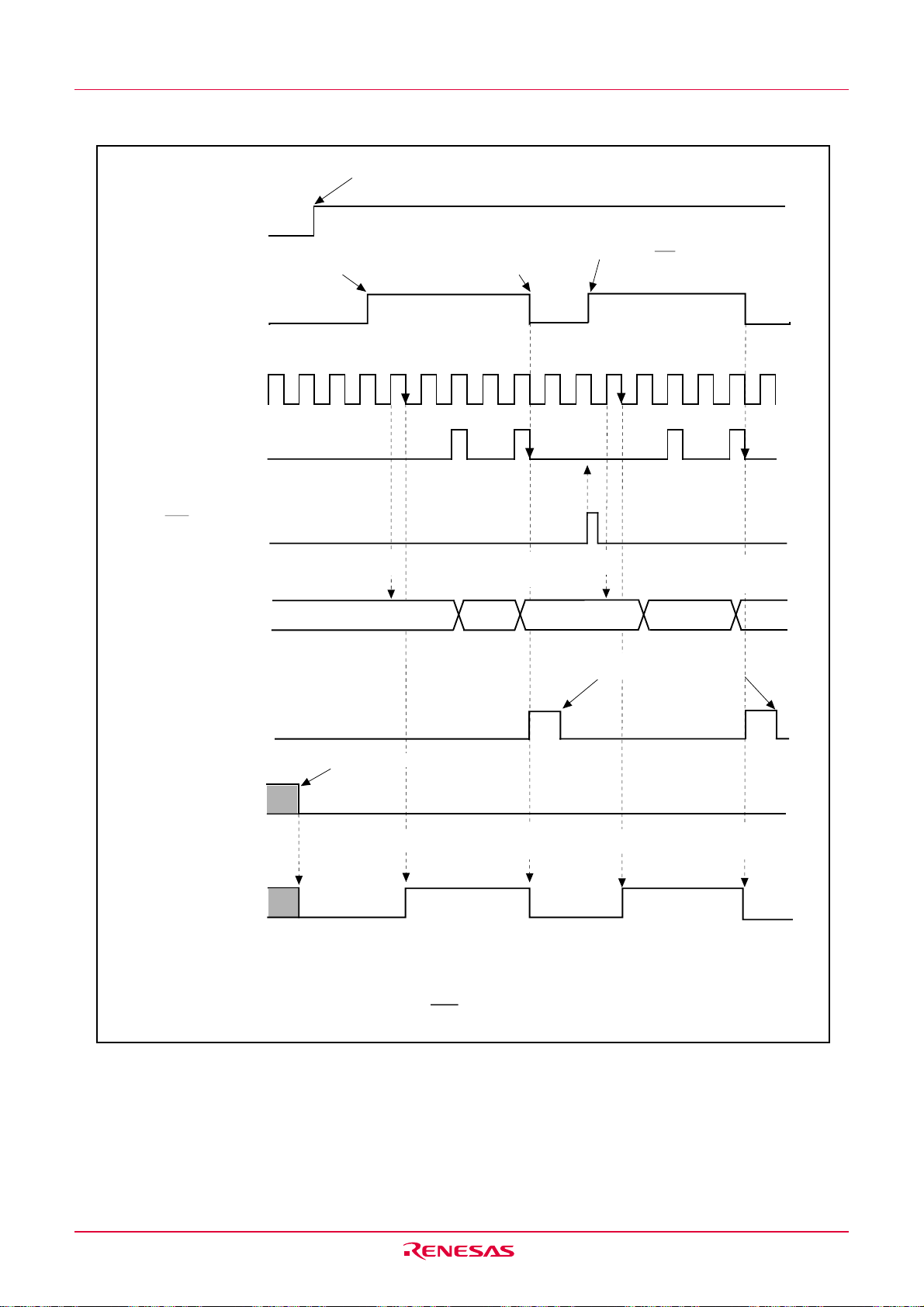
R8C/12 Group
12.3 Timer (Timer Z)
Set to “1” by program
TZS bit in
TYZMR register
TZOS bit in
TYZOC register
Count source
Prescaler Z
underflow signal
INT0 pin input
Contents of Timer Z
“1”
“0”
Set to “1” by program
“1”
“0”
“1”
“0”
01
Count
starts
16
Set to “0” when count
completes
Timer Z
primary
reload
00
16
Set to “1” by INT0 pin
input trigger
Count
starts
00
01
16
Set to “0” when interrupt request
is acknowledged or by program
16
Timer Z
primary
reload
01
16
IR bit in
TZIC register
TZOPL bit in
PUM register
“1”
“0”
“1”
“0”
Set to “1” by program
Waveform
output starts
Waveform
output
completes
Waveform
output starts
“H”
TZ
OUT
pin output
“L”
The above applies to the following conditions;
PREZ=01
16
, TZPR=01
16
TZOPL bit in PUM register=0, INOSTG bit= 1(INT0 one-shot trigger enabled)
INOSEG bit= 1(rising edge trigger)
Figure 12.25 Operation Example in Programmable One-shot Generation Mode
Waveform
output
completes
Rev.1.20 Jan 27, 2006 page 82 of 181
REJ09B0110-0120
Page 93

R8C/12 Group
12.3 Timer (Timer Z)
12.3.4 Programmable Wait One-shot Generation Mode
In this mode, upon program or external trigger input (input to the INT0 pin), the microcomputer outputs
the one-shot pulse from the TZOUT pin after waiting for a given length of time (see “Table 12.12
Programmable Wait One-shot Generation Mode Specifications”). When a trigger occurs, from this
point, the timer starts outputting pulses only once for a given length of time equal to the set value in the
TZSC register after waiting for a given length of time equal to the set value in the TZPR register.
Figure 12.26 shows the TYZMR and PUM registers in this mode. Figure 12.27 shows an operation
example in this mode.
Table 12.12 Programmable Wait One-shot Generation Mode Specifications
Item Specification
Count source f1, f2, f8, Timer Y underflow
Count operation • Downcounts set value in Timer Z primary
• When a counting of TZPR register underflows, the timer reloads the contents of TZSC
register before continuing counting.
• When a counting of TZSC register underflows, the timer reloads the contents of TZPR
register before completing counting.
• When a count stops, the timer reloads the contents of the reload register before it stops.
Wait time (n+1)(m+1)/fi n: set value in PREZ register, m: set value in TZPR register
One-shot pulse output time (n+1)(p+1)/fi n : set value in PREZ, p: set value in TZSC register
(2)
(start one-shot)
Count start condition • Set TZOS bit in TYZOC register to “1”
_______
• Input active trigger to INT0 pin
Count stop condition • When reloading is completed after count value at counting TZSC register was set to
16"
"00
• When TZS bit in TYZMR register is set to “0” (stop counting)
• When TZOS bit in TYZOC register is set to “0” (stop one-shot)
Interrupt request generation timing
In half cycles of count source, after count value at counting TZSC register is set "0016"
(at the same time as the TZout output change) [Timer Z interrupt]
TZ
OUT pin function Pulse output
_______
INT0 pin function
Use timer mode when using this pin as a programmable I/O port.
_______
Programmable I/O port, INT0 interrupt input or external trigger input
• When the INOSTG bit in the PUM register is set to “0” (INT0 one-shot trigger disabled)
_______
Programmable I/O port or INT0 interrupt input
• When the INOSTG bit in the PUM register is set to “1” (INT0 one-shot trigger enabled)
_______
external trigger (INT0 interrupt input)
Read from timer Count value can be read out by reading TZPR register.
Same applies to PREZ register.
Write to timer
Value written to TZPR register and PREZ register are written to reload register only
Same applies to TZSC register.
Select function • Output level latch select function
Output level for one-shot pulse waveform is selected by TZOPL bit.
_______
• INT0 pin one-shot trigger control function and polarity select function
_______
Trigger input from INT0 pin can be set to active or inactive by INOSTG bit. Also, an
active trigger's polarity can be selected by INOSEG bit.
NOTES:
1. The TZS bit in the TYZMR register must be set to "1" (start counting).
2. The TZS bit must be set to "1" (start counting), the INT0EN bit in the INTEN register to "1" (enabling INT0 input), and
the INOSTG bit in the PUM register to "1" (enabling INT0 one-shot trigger).
Although the trigger input during counting cannot be acknowledged, the INT0 interrupt request is generated.
_______
3. The set values are reflected beginning with the next one-shot pulse after writing to the TZPR register.
(1)
_______
_______
_______
(3)
.
Rev.1.20 Jan 27, 2006 page 83 of 181
REJ09B0110-0120
Page 94
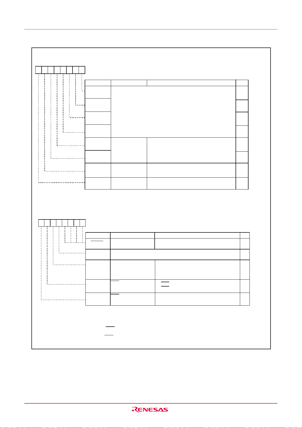
R8C/12 Group
b7b6b5b4b3b2b1b
L
r
000
0
b
b
b5b
b
b
b
b
12.3 Timer (Timer Z)
T i m e r Y , Z m o d e r e g i s t e r
7
6
4
11
1
3
2
1
d d r e s
f t e r r e s e
0 8
0
S y m b o lA
T Y Z M R0
B i t n a m e
TYMOD0
Timer Y-related bit
sA
0
1 6
0 0
t
1 6
F u n c t i o nB i t s y m b o l
R 1 E D G
T Y W C
T Y S
b5 b4
1 1 : P r o g r a m m a b l e w a i t o n e - s h o t g e n e r a t i o n
m o d e
T Z M O D 0
Timer Z operation
mode bit
T Z M O D 1
N O T E S :
TZWC
T Z S
Timer Z write
control bit
Timer Z count
start flag
Must set to "1" in programmable wait one-shot
generation mode
(1)
0 : S t o p s c o u n t i n g
1 : S t a r t s c o u n t i n g
1 . W h e n T Z S b i t = 1 ( s t a r t s c o u n t i n g ) , t h e t i m e r Z c o u n t v a l u e i s w r i t t e n t o t h e r e l o a d r e g i s t e r o n l y .
W h e n T Z S b i t = 0 ( s t o p s c o u n t i n g ) , t h e t i m e r Z c o u n t v a l u e i s w r i t t e n t o b o t h r e l o a d r e g i s t e r a n d c o u n t e r .
R W
R W
R W
R W
R W
R W
RW
R W
RW
T i m e r Y , Z w a v e f o r m o u t p u t c o n t r o l r e g i s t e r
0
Symbol Address After reset
PUM 0084
Bit symbol
(b3-b0)
TYOP
TZOPL
INOSTG
INOSEG
B i t n a m e
Reserved bit
T i m e r Y - r e l a t e d b i t
T i m e r Z o u t p u t l e v e l
l a t c h
I N T 0 p i n o n e - s h o t t r i g g e
c o n t r o l b i t
I N T 0 p i n o n e - s h o t t r i g g e r
p o l a r i t y s e l e c t b i t
N O T E S :
1 . T h e I N O S E G b i t i s v a l i d o n l y w h e n t h e I N T 0 P L b i t i n t h e I N T E N r e g i s t e r i s s e t t o " 0 " ( o n e - e d g e ) .
2 . T h e I N O S G T b i t m u s t b e s e t t o “ 1 ” a f t e r t h e I N T 0 E N b i t i n t h e I N T E N r e g i s t e r a n d t h e I N O S E G b i t i n t h e P U M r e g i s t e r a r e
s e t .
W h e n s e t t i n g t h e I N O S T G b i t t o " 1 " ( I N T 0 p i n o n e - s h o t t r i g g e r e n a b l e d ) , t h e I N T 0 F 0 a n d I N T 0 F 1 b i t s i n t h e I N T 0 F r e g i s t e r
m u s t b e s e t .
T h e I N O S T G b i t m u s t b e s e t t o “ 0 ” ( I N T 0 p i n o n e - s h o t t r i g g e r d i s a b l e d ) a f t e r t h e T Z S b i t i n t h e T Y Z M R r e g i s t e r i s s e t t o “ 0 ”
( c o u n t s t o p ) .
Figure 12.26
TYZMR Register and PUM Register
16
00
16
Function
Must set to “0”
0 : Outputs "H" level one-shot pulse.
Outputs "L" when the timer is stopped.
1 : Outputs "L" level one-shot pulse
Outputs "H" when the timer is stopped.
(2 )
(1 )
0 : INT0 pin one-shot trigger disabled
1 : INT0 pin one-shot trigger enabled
0 : Edge trigger at falling edge
1 : Edge trigger at rising edge
(2)
in Programmable Wait One-shot Generation Mode
R W
R W
R W
RW
R W
R W
Rev.1.20 Jan 27, 2006 page 84 of 181
REJ09B0110-0120
Page 95

R8C/12 Group
W
T i
Z
C
T i
W
W
12.3 Timer (Timer Z)
S e t t o “1” b y p r o g r a m
T Z S b i t i n
T Y Z M R r e g i s t e r
TZOS bit in
TYZOC register
C o u n t s o u r c e
P r e s c a l e r Z
u n d e r f l o w s i g n a l
INT0 input pin
“ 1 ”
“ 0 ”
S e t t o “1” b y p r o g r a m o r “1” b y I N T0 p i n i n p u t
t r i g g e r
“ 1 ”
“ 0 ”
“ 1 ”
“0”
o u n t
s t a r t s
m e r
s e c o n d a r y
r e l o a d
Set to “0” when coun t
completes
m e r Z
p r i m a r y
r e l o a d
Contents of Timer Z
IR bit in
TZIC register
T Z O P L b i t i n
P U M r e g i s t e r
T Z
O U T
p i n o u t p u t
T h e a b o v e a p p l i e s t o t h e f o l l o w i n g c o n d i t i o n s ;
P R E Z = 0 1
T Z O P L b i t i n P U M r e g i s t e r = 0 , I N O S T G b i t = 1 ( I N T 0 o n e - s h o t t r i g g e r e n a b l e d )
I N O S E G b i t = 1 ( r i s i n g e d g e t r i g g e r )
“ 1 ”
“0”
“1”
“0”
“ H ”
“ L ”
1 6
, T Z P R = 0 1
01
16
Set to “0” by prog r am
a i t s t a r t
s
1 6
, T Z S C = 0 2
1 6
00
16
a v e f o r m
o u t p u t s t a r t s
02
0 1
16
01
16
00
16
Set to “0” when interrupt request
is acknowledged or by program
output
completes
1 6
aveform
Figure 12.27 Operation Example in Programmable Wait One-shot Generation Mode
Rev.1.20 Jan 27, 2006 page 85 of 181
REJ09B0110-0120
Page 96

R8C/12 Group
12.4 Timer (Timer C)
12.4 Timer C
Timer C is a 16-bit free-running timer. Figure 12.28 shows a block diagram of Timer C. The Timer C uses
an edge input to TCIN pin or the fRING128 clock as trigger to latch the timer count value and generates an
interrupt request. The TCIN input has a digital filter and this prevents an error caused by noise or so on
from occurring. Table 12.13 shows Timer C specifications. Figure 12.29 shows TC, TM0, TCC0, and
TCC1 registers. Figure 12.30 shows an operation example of Timer C.
Data bus
Lower 8 bits
Lower 8 bits
Counter
Transfer signal
TCC11 to TCC10
INT3/TC
IN
Other than 00
TCC11 to TCC10
f
1
f
8
f
32
TCC02 to TCC01
f
f
f
32
2
=00
Digital
2
=01
2
=10
2
=11
2
Sampling
clock
1
8
filter
f
RING128
=00
=01
=10
2
2
2
TCC07=0
TCC07=1
Upper 8 bits
TM0 register
Upper 8 bits
TC register
Edge detection
TCC01, TCC02, TCC07: Bits in TCC0 register
TCC10, TCC11: Bits in TCC1 register
Figure 12.28 Timer C Block Diagram
Table 12.13 Timer C Specifications
Item Specification
Count source f1, f8, f32
Count operation • Count up
• Transfer value in TC register to TM0 register at active edge of measurement pulse
• Value in TC register is set to “000016” when a counting stops
Count start condition TCC00 bit in TCC0 register is set to “1” (capture enabled)
Count stop condition TCC00 bit in TCC0 register is set to “0” (capture disabled)
I
nterrupt request
generation timing • When Time C underflows [Timer C interrupt]
______
INT3/TCIN pin function Programmable I/O or measurement pulse input
• When active edge of measurement pulse is input [INT3 interrupt]
Counter value reset timing When TCC00 bit in TCC0 register is set to “0” (capture disabled)
Read from timer
(1)
• Counter value can be read out by reading TC register.
• Counter value at measurement pulse active edge input can be read out by reading TM0
register.
Write to timer Write to TC register and TM0 register is disabled
Select function
_____
• INT3/TCIN switching function
Measurement pulse active edge is selected by TCC03 to TCC04 bits
• Digital filter function
Digital filter sampling frequency is selected by TCC11 to TCC10 bits
• Trigger select function
TCIN input or fRING128 is selected by TCC07 bit.
NOTES:
1. TC register and TM0 register must be read in 16-bit units.
_____
Timer C interrupt
INT3 interrupt
Rev.1.20 Jan 27, 2006 page 86 of 181
REJ09B0110-0120
Page 97

R8C/12 Group
b
b0b
b
( b
)
(b8)
b
b0b
b
( b
)
( b
)
b
b
b
b
b
b
b
b
b7b6b5b4b3b2b1b
00000
0
T i m e r C r e g i s t e r
1 5
7
12.4 Timer (Timer C)
7
0
Symbol Address After reset
TC 0091
16
-0090
16
0000
16
C a p t u r e r e g i s t e r
1 5
7
T i m e r C c o n t r o l r e g i s t e r 0
7
6
5
8
7
0
4
3
2
1
0
00
F u n c t i o n
I n t e r n a l c o u n t s o u r c e i s c o u n t e d
" 0 0 0 0
c a n b e r e a d o u t b y r e a d i n g w h e n T C C 0 0 b i t = 0 ( s t o p s c o u n t i n g )
"
1 6
C o u n t v a l u e c a n b e r e a d o u t b y r e a d i n g w h e n T C C 0 0 b i t = 1 ( s t a r t c o u n t i n g )
Symbol Address After reset
TM0 009D
16
-009C
16
0000
16
F u n c t i o n
When active edge of measurement pulse is input, the counter value of
Timer C is stored
d d r e s
f t e r r e s e
0 9
S y m b o lA
T C C 00
Bit name
TCC00
TCC01
TCC02
TCC03
TCC04
( b 6 - b 5 )
Timer C count start bit
Timer C count source select
(1)
bit
INT3 interrupt and
capture input polarity select
(1, 2)
bit
r e s e r v e d b i t
sA
A
1 6
0 : C o u n t s t o p
1 : C o u n t s t a r t
b 2 b 1
0 0 : f
0 1 : f
1 0 : f
1 1 : Avoid this setting
b 4 b 3
0 0 : Rising edge
0 1 : Falling edge
1 0 : Both edges
1 1 : Avoid this setting
S e t t o " 0 "
t
0 0
1 6
F u n c t i o nB i t s y m b o l
1
8
32
R W
R O
R W
RO
RW
RW
R W
R W
R W
R W
RW
T C C 0 7
I N T 3 i n t e r r u p t a n d
c a p t u r e i n p u t s w i t c h i n g b i t
(1 , 2 )
0 : I N T 3
1 : f
R I N G 1 2 8
N O T E S :
1 . C h a n g e t h i s b i t w h e n T C C 0 0 b i t i s s e t t o “ 0 ” ( c o u n t s t o p ) .
2 . T h e I R b i t i n t h e I N T 3 I C m a y b e s e t t o “ 1 ” ( i n t e r r u p t r e q u e s t e d ) w h e n t h e T C C 0 3 , T C C 0 4 , o r T C C 0 7 b i t i s r e w r i t t e n .
R e f e r t o t h e p a r a g r a p h 1 9 . 2 . 5 “ C h a n g i n g I n t e r r u p t F a c t o r ” i n t h e U s a g e N o t e s R e f e r e n c e B o o k .
T i m e r C c o n t r o l r e g i s t e r 1
d d r e s
f t e r r e s e
0 9
0
S y m b o lA
T C C 10
B i t n a m e
T C C 1 0
INT3 input filter select bit
sA
B
1 6
(1)
t
0 0
1 6
b 1 b 0
0 0 : No filter
F u n c t i o nB i t s y m b o l
0 1 : Filter with f
T C C 1 1
(b7-b2)
R e s e r v e d b i t
1 0 : Filter with f
1 1 : Filter with f
S e t t o " 0 "
N O T E S :
1 . I n p u t i s r e c o g n i z e d o n l y w h e n t h e s a m e v a l u e f r o m I N T 3 p i n i s s a m p l e d t h r e e t i m e s i n s u c c e s s i o n .
Figure 12.29 TC Register, TM0 Register, TCC0 Register, and TCC1 Register
Rev.1.20 Jan 27, 2006 page 87 of 181
REJ09B0110-0120
1
sampling
8
sampling
32
sampling
RW
RW
RW
R W
RW
Page 98

R8C/12 Group
12.4 Timer (Timer C)
FFFF16
Counter contents (hex)
TCC00 bit in TCC0
register
Measurement pulse
(TC
IN
pin input)
Transmit timing from
Timer C counter to
TM0 register
000016
“1”
“0”
“H”
Count start
Set to "1" by program
The delay caused
by digital filter
“L”
Measurement value 1
Transmit
(Measurement
value 1)
Measurement value 2
Transmit
(Measurement
value 2)
Overflow
Measurement
value 3
Set to "0" by
program
Transmit
(Measurement
value 3)
Time
Indeterminate
TM0 register
Measurement
value 1
Set to “0” when interrupt request is accepted, or set by program
IR bit in INT3IC
register
IR bit in TCIC
register
“1”
“0”
“1”
“0”
Conditions: TCC0 register TCC04 to TCC03 bits=012 (capture input polarity is set for falling edge),
TCC07=0 (INT3/TC
IN
input as capture input trigger)
Figure 12.30 Operation Example of Timer C
Indeterminate
Measurement value 2
Measurement
value 3
Set to “0” when interrupt
request is accepted, or set by
program
Rev.1.20 Jan 27, 2006 page 88 of 181
REJ09B0110-0120
Page 99

R8C/12 Group 13. Serial Interfaces
13. Serial Interface
Serial interface is configured with two channels: UART0 to UART1. UART0 and UART1 each have an
exclusive timer to generate a transfer clock, so they operate independently of each other.
Figure 13.1 shows a block diagram of UARTi (i=0, 1). Figure 13.2 shows a block diagram of the UARTi
transmit/receive.
UART0 has two modes:
mode).
UART1 has only one mode,
Figures 13.3 to 13.5 show the UARTi-related registers.
clock synchronous serial I/O mode, and clock asynchronous serial I/O mode (UART
clock asynchronous serial I/O mode (UART mode).
(UART0)
RxD0
CLK1 to CLK0=002
f
1SIO
=012
f
8SIO
=102
f
32SIO
CLK0
(UART1)
RxD1
CLK1 to CLK0=002
f
1SIO
f
8SIO
f
32SIO
CLK
polarity
reversing
circuit
=012
=102
Main clock or on-chip oscillator clock
Internal
U0BRG register
1/(n0+1)
External
Clock synchronous type
(when internal clock is selected)
TXD1EN
U1BRG
Internal
register
1/(n1+1)
UART reception
1/16
Clock synchronous
type
UART transmission
1/16
Clock synchronous
type
Clock synchronous type
(when internal clock is selected)
1/2
Clock synchronous type
(when external clock is selected)
UART reception
1/16
UART transmission
1/16
1/8
Reception
control circuit
Transmission control
circuit
CKDIR=0
CKDIR=1
Reception
control circuit
Transmission
control circuit
1/4
f
1SIO
f
8SIO
f
32SIO
Receive
clock
Transmit
clock
Reception
control circuit
Transmission
control circuit
Transmit/
receive
unit
Transmit/
receive
unit
TXD1SEL=1
TXD1SEL=0
To P00
TxD
0
TxD10
TxD11
Figure 13.1 UARTi (i=0, 1) Block Diagram
Rev.1.20 Jan 27, 2006 page 89 of 181
REJ09B0110-0120
Page 100

R8C/12 Group 13. Serial Interface
PAR
U A R T
)
PAR
Clock
synchronous
type
UART (7 bits)
UART (8 bits)
( 9 b i t s
UART (7 bits)
Clock
synchronous type
UART (8 bits)
UART (9 bits)
UARTi receive register
R x D i
1SP
S PS
P
2SP
P R Y E = 0
P A R
d i s a b l e d
P A R
e n a b l e d
P R Y E = 1
C l o c k
s y n c h r o n o u s
t y p e
U A R T
0000000
P R Y E = 1
PAR
UART
2 S P
enabled
SP SP
1SP
PAR
disabled
P R Y E = 0
Clock
synchronous
type
“0”
Figure 13.2 UARTi Transmit/Receive Unit
D
8
D a t a b u s h i g h - o r d e r b i t s
D a t a b u s l o w - o r d e r b i t s
D
8
UART (8 bits)
UART (9 bits)
U A R T ( 9 b i t s )
UART (7 bits)
UART (8 bits)
Clock
synchronous type
Clock
synchronous
type
D7D6D5D4D3D2D1D
MSB/LSB conversion circuit
M S B / L S B c o n v e r s i o n c i r c u i t
D7D6D5D4D3D2D1D
UART (7 bits)
NOTES:
1. Clock synchronous typ e is pr ov ide in UART0 only.
UARTi transmit register
i = 0 , 1
S P : S t o p b i t
P A R : P a r i t y b i t
U i R B r e g i s t e r
0
UiTB register
0
T x D i
Rev.1.20 Jan 27, 2006 page 90 of 181
REJ09B0110-0120
 Loading...