

Page 1
3
9-0140
REJ10B02
M3S-UFLA32R
User’s Manual
UART Flash Memory Programming Utility
All information contained in these materials, including products and product specifications,
represents information on the product at the time of publication and is subject to change by
Renesas Technology Corp. without notice. Please review the latest information published
by Renesas Technology Corp. through various means, including the Renesas Technology
Corp. website (http://www.renesas.com).
Rev.1.40
Revision Date: Mar. 06, 2007
Page 2

Notes regarding these materials
1. This document is provided for reference purposes only so that Renesas customers may select the appropriate
Renesas products for their use. Renesas neither makes warranties or representations with respect to the
accuracy or completeness of the information contained in this document nor grants any license to any
intellectual property rights or any other rights of Renesas or any third party with respect to the information in
this document.
2. Renesas shall have no liability for damages or infringement of any intellectual property or other rights arising
out of the use of any information in this document, including, but not limited to, product data, diagrams, charts,
programs, algorithms, and application circuit examples.
3. You should not use the products or the technology described in this document for the purpose of military
applications such as the development of weapons of mass destruction or for the purpose of any other military
use. When exporting the products or technology described herein, you should follow the applicable export
control laws and regulations, and procedures required by such laws and regulations.
4. All information included in this document such as product data, diagrams, charts, programs, algorithms, and
application circuit examples, is current as of the date this document is issued. Such information, however, is
subject to change without any prior notice. Before purchasing or using any Renesas products listed in this
document, please confirm the latest product information with a Renesas sales office. Also, please pay regular
and careful attention to additional and different information to be disclosed by Renesas such as that disclosed
through our website. (http://www.renesas.com )
5. Renesas has used reasonable care in compiling the information included in this document, but Renesas
assumes no liability whatsoever for any damages incurred as a result of errors or omissions in the information
included in this document.
6. When using or otherwise relying on the information in this document, you should evaluate the information in
light of the total system before deciding about the applicability of such information to the intended application.
Renesas makes no representations, warranties or guaranties regarding the suitability of its products for any
particular application and specifically disclaims any liability arising out of the application and use of the
information in this document or Renesas products.
7. With the exception of products specified by Renesas as suitable for automobile applications, Renesas
products are not designed, manufactured or tested for applications or otherwise in systems the failure or
malfunction of which may cause a direct threat to human life or create a risk of human injury or which require
especially high quality and reliability such as safety systems, or equipment or systems for transportation and
traffic, healthcare, combustion control, aerospace and aeronautics, nuclear power, or undersea communication
transmission. If you are considering the use of our products for such purposes, please contact a Renesas
sales office beforehand. Renesas shall have no liability for damages arising out of the uses set forth above.
8. Notwithstanding the preceding paragraph, you should not use Renesas products for the purposes listed below:
(1) artificial life support devices or systems
(2) surgical implantations
(3) healthcare intervention (e.g., excision, administration of medication, etc.)
(4) any other purposes that pose a direct threat to human life
Renesas shall have no liability for damages arising out of the uses set forth in the above and purchasers who
elect to use Renesas products in any of the foregoing applications shall indemnify and hold harmless Renesas
Technology Corp., its affiliated companies and their officers, directors, and employees against any and all
damages arising out of such applications.
9. You should use the products described herein within the range specified by Renesas, especially with respect
to the maximum rating, operating supply voltage range, movement power voltage range, heat radiation
characteristics, installation and other product characteristics. Renesas shall have no liability for malfunctions or
damages arising out of the use of Renesas products beyond such specified ranges.
10. Although Renesas endeavors to improve the quality and reliability of its products, IC products have specific
characteristics such as the occurrence of failure at a certain rate and malfunctions under certain use
conditions. Please be sure to implement safety measures to guard against the possibility of physical injury, and
injury or damage caused by fire in the event of the failure of a Renesas product, such as safety design for
hardware and software including but not limited to redundancy, fire control and malfunction prevention,
appropriate treatment for aging degradation or any other applicable measures. Among others, since the
evaluation of microcomputer software alone is very difficult, please evaluate the safety of the final products or
system manufactured by you.
11. In case Renesas products listed in this document are detached from the products to which the Renesas
products are attached or affixed, the risk of accident such as swallowing by infants and small children is very
high. You should implement safety measures so that Renesas products may not be easily detached from your
products. Renesas shall have no liability for damages arising out of such detachment.
12. This document may not be reproduced or duplicated, in any form, in whole or in part, without prior written
approval from Renesas.
13. Please contact a Renesas sales office if you have any questions regarding the information contained in this
document, Renesas semiconductor products, or if you have any other inquiries.
Page 3

Precautions on Using The Product Described Herein
1. The product described herein should be used in combination with the parts included with
the starter kit. If the product is operated in combination with any other item, its operation
cannot be guaranteed. Nor will requests for help or suggestion be answered.
2. The product described herein was prepared for program development or evaluation
purposes. The product cannot be used for the mass production.
3. Renesas Technology Corporation and Renesas Solutions Corporation will not assume any
responsibility for the results of development no matter what systems may have been
developed by customers by using the product described herein.
4. Guarantee for the product described herein shall conform to stipulations under which
guarantee is provided for the starter kit.
5. The product described herein was prepared assuming it will be used in a laboratory or
similar environment for program development or evaluation purposes. It is not covered in
the electrical product safety laws, nor is it protected against electromagnetic hazards for
use in Japan or elsewhere.
For Inquiries About Product Contents or This Manual
Please contact:
Renesas Technology Corporation
at csc@renesas.com
* Microsoft, MS-DOS, Windows, and Windows NT are registered trademarks of Microsoft Corporation in the U.S. and
other countries.
* Adobe and Acrobat are registered trademarks of Adobe Systems Incorporated.
* All other brand names and product names are trademarks or registered trademarks of each proprietary company.
Page 4

Contents
1. Overview .......................................................................................................................1
2. System Configuration ....................................................................................................1
2.1 Outline of the M3S-UFLA32R................................................................................................................ 1
2.2 Communication Cable (M3A-2145G50) ................................................................................................ 2
2.3 Target MCU/Target Board...................................................................................................................... 4
2.4 Host PC ................................................................................................................................................. 4
3. Installation of the M3S-UFLA32R..................................................................................5
3.1 Installation of the M3S-UFLA32R.......................................................................................................... 5
4. Operation Method of the M3S-UFLA32R ......................................................................6
4.1 Startup ................................................................................................................................................... 6
4.2 Exit......................................................................................................................................................... 6
4.3 Operation Outline of the M3S-UFLA32R............................................................................................... 6
5. Function Description of the M3S-UFLA32R ..................................................................8
5.1 Function list ........................................................................................................................................... 8
5.2 Program Data (Motorola S-format file) Selection .................................................................................. 9
5.3 Exit the Application .............................................................................................................................. 10
5.4 Lock Bit Information..............................................................................................................................11
5.5 Program............................................................................................................................................... 13
5.6 Erase ................................................................................................................................................... 14
5.7 Block Erase ......................................................................................................................................... 15
5.8 Lock Bit/Set ......................................................................................................................................... 17
5.9 Lock Bit/Enable.................................................................................................................................... 19
5.10 Lock Bit/Disable................................................................................................................................. 20
5.11 Blank Check....................................................................................................................................... 21
5.12 Verify Check ...................................................................................................................................... 22
5.13 E.B.P.V. (Erase, Blank Check, Program, Verify Check) .................................................................... 23
5.14 E.P. (Erase, Program)........................................................................................................................ 23
5.15 B.P.V. (Blank Check, Program, Verify Check) ................................................................................... 24
5.16 Setting ............................................................................................................................................... 25
5.17 ID Code Setting ................................................................................................................................. 27
5.18 Version Information ........................................................................................................................... 29
6. Error Message List ......................................................................................................30
Contents-1
Page 5
M3S-UFLA32R
UART Flash Memory Programming Utility
1. Overview
This user’s manual is intended to provide explanations about system configuration and operation
method of the UART Flash Memory Programming Utility M3S-UFLA32R Ver.1.40 (hereinafter
referred to as M3S-UFLA32R) for the M32R/ECU Series (Refer to the Table 2.3.1 for
corresponding MCU).
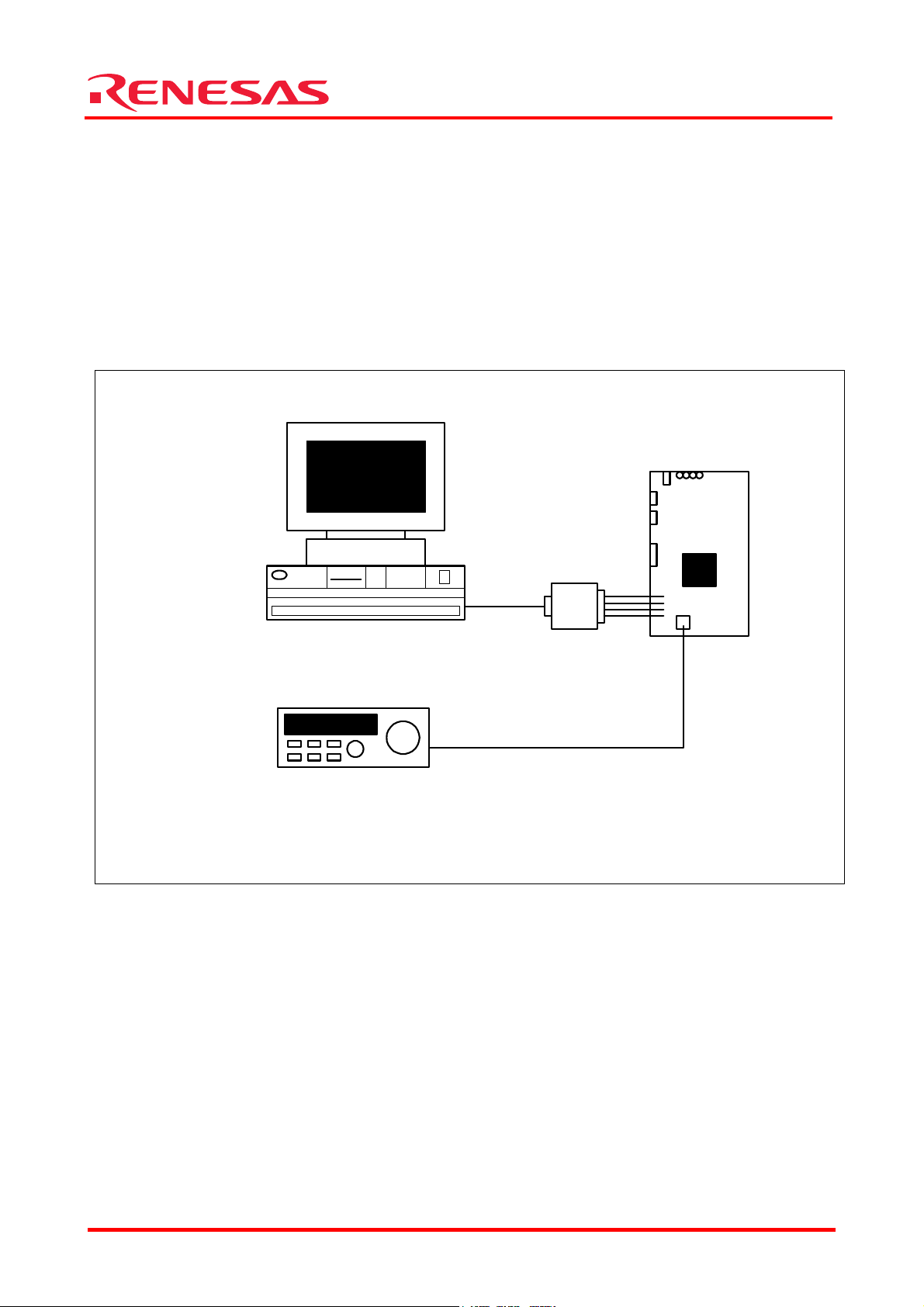
2. System Configuration
Figure 2.1.1 shows connection configuration of the system using the M3S-UFLA32R
Target Board
Host PC
Communication
Cable
(M3A-2145G50)
DC Power Supply
Figure 2.1.1 Connection Configuration
2.1 Outline of the M3S-UFLA32R
The M3S-UFLA32R is a Windows application program that performs UART communication with
SIO1 of a MCU serial interface by the boot program built into a MCU (flash programming
firmware) and executes write/erase operation to the MCU flash memory.
REJ10B0239-0140/Rev.1.40 Mar. 2007 Page 1 of 30
Page 6
M3S-UFLA32R
UART Flash Memory Programming Utility
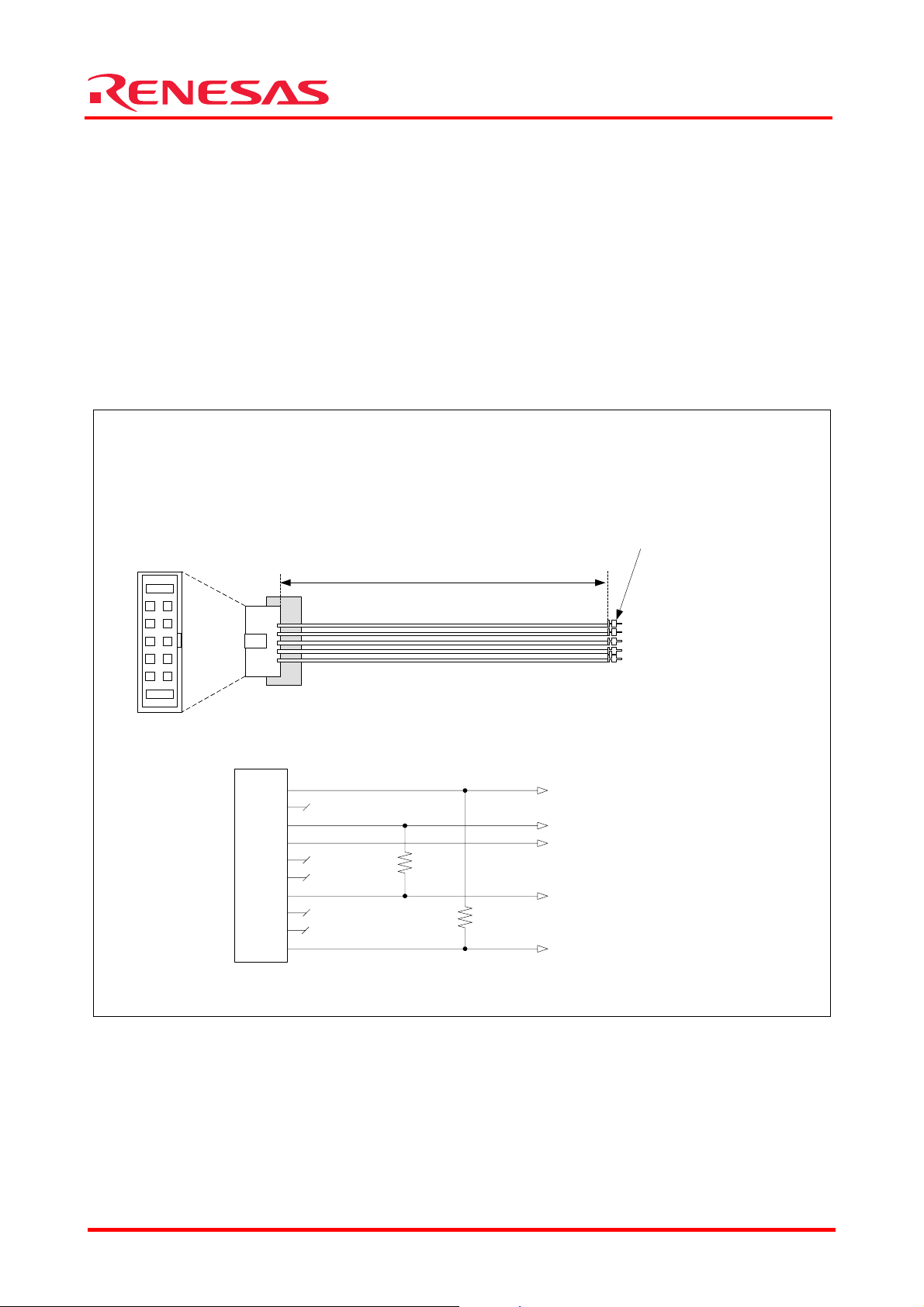
2.2 Communication Cable (M3A-2145G50)
Communication cable consists of two different cables below.
•Interface Cable (M3A-2145G02)
It is a conversion cable to connect to the test pins on the target when the connection cable for the
MF-TEN-NINE can not be mounted on the target board. Figure 2.2.1 shows connecting diagram.
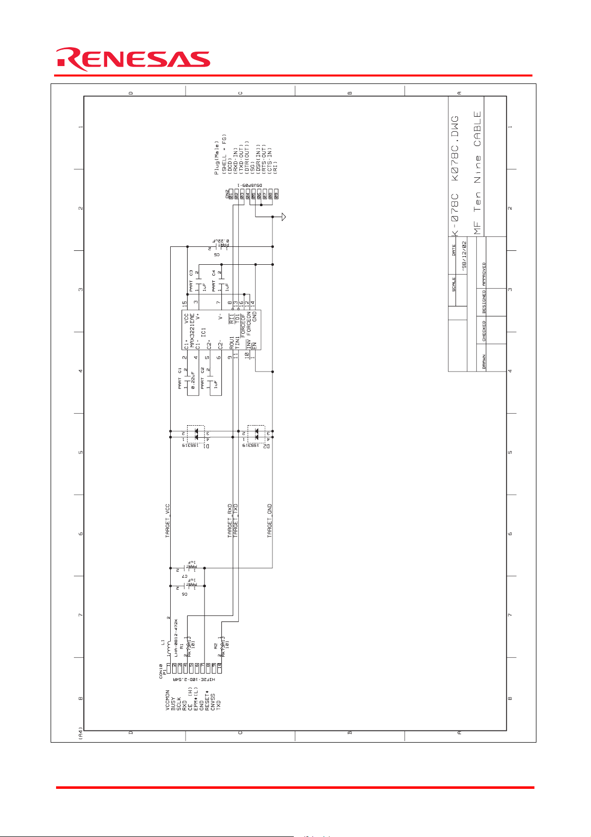
•MF-TEN-NINE Cable (M3A-0652CBL)
It is a cable to connect host PC to target board. Figure 2.2.2 shows connecting diagram.
Communication cable receives power supply from the target board. The power supply voltage can
be used at 3.3V or 5.0V.
Table 2.2.1 shows usage specification of the communication cable.
Connector (Manufactured by Hirose Electric Co., Ltd.
HIF3FC-10PA-2.54DSA)
10-pin Connector (Male)
Cable side (Front side)
IC Clip (Miyama Electric Company., Ltd
MJ-033)
Add label to IC Clip (Pin Name)
10 2
9 1
NC
NC
NC
NC
NC
10
1
2
3
4
5
6
7
8
9
47KΩ
VCC
SCLK
RXD
GND
TXD
150mm
47KΩ
Figure 2.2.1 Interface Cable Connecting Diagram
Lable name of IC clip
and color of wiring
coatings
VCC
(Red)
RXD
GND
TXD
(Blue)
(Yellow)
(Black)
(Green)
SCLK
REJ10B0239-0140/Rev.1.40 Mar. 2007 Page 2 of 30
Page 7
M3S-UFLA32R
UART Flash Memory Programming Utility
RJJ99J0021-0100
Figure 2.2.2 MF-TEN-NINE Cable Connecting Diagram
REJ10B0239-0140/Rev.1.40 Mar. 2007 Page 3 of 30
Page 8
UART Flash Memory Programming Utility
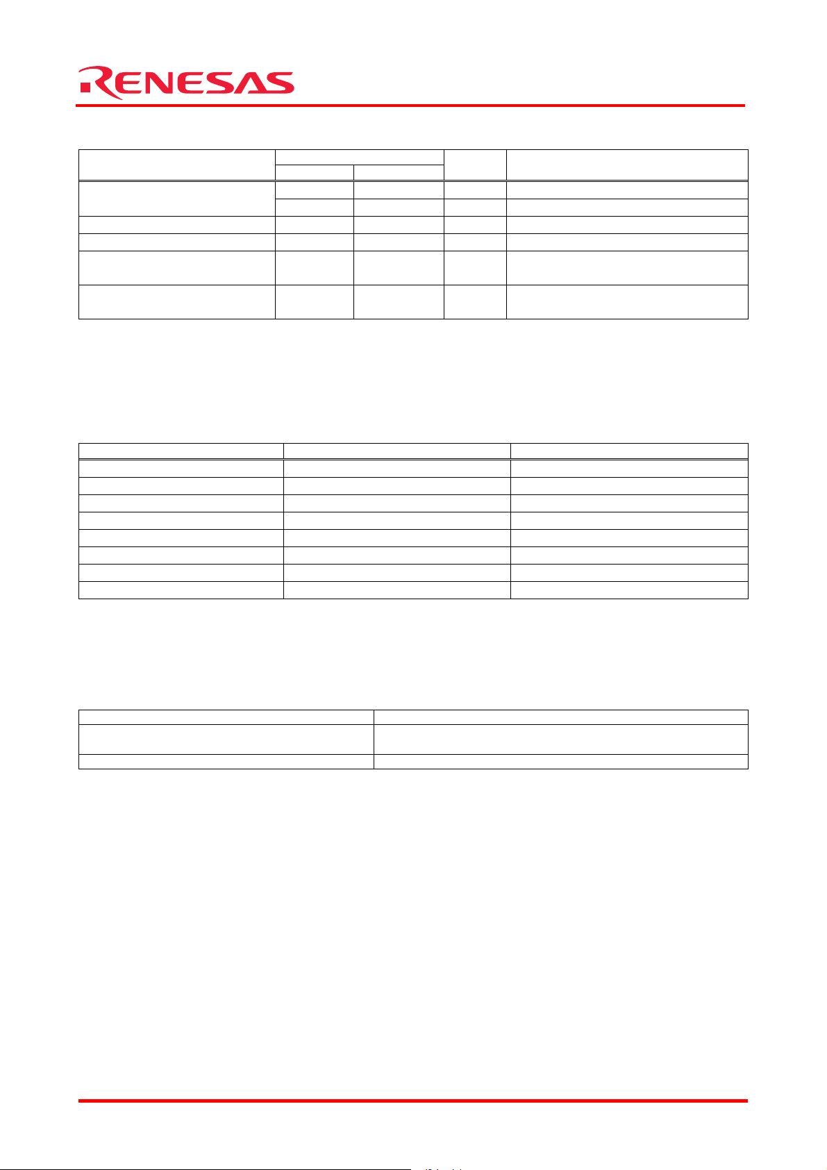
Table 2.2.1 Usage Specification
Parameter
DC Power Supply
RS-232C Communication Rate
Consumption Current
Operating Ambient Temperature
Storage Ambient Temperature
Rated Value
MIN MAX
3.0 3.6 V Target Supply Voltage
4.5 5.5 V Target Supply Voltage
9600 115200 bps Communication Speed with PC
- 60 mA MAX3221EAE Specification
5 35 °C
0 60 °C
Unit Condition
No Condensation, No Corrosive Gas
Environment
No Condensation, No Corrosive Gas
Environment
2.3 Target MCU/Target Board
Target MCU and Target Board should be prepared by the user.
Table 2.3.1 lists the M3S-UFLA32R compatible MCUs and Target Boards.
Table 2.3.1 Target MCU and Target Board
Target MCU Target Board Type Name Starter Kit Type Name
32170/32174 Group
32171 Group
32172/32173 Group
32176 Group
32180 Group
32182 Group
32185/32186 Group
32192/32195/32196 Group
M3A-2114G02 M3A-2114G52, M3A-2114G52A
M3A-2114G12 M3A-2114G62, M3A-2114G62A
M3A-2114G22 M3A-2114G72, M3A-2114G72A
M3A-2152G02 M3A-2152G52, M3A-2152G52A
M3A-2142G02 M3A-2142G52, M3A-2142G52A
M3A-2142G12 M3A-2142G62, M3A-2142G62A
M3A-2154G02A M3A-2154G52B
M3A-2154G02, M3A-2154G02A M3A-2154G52A, M3A-2154G52B
M3S-UFLA32R
2.4 Host PC
Table 2.4.1 shows the system requirements of a host PC. Host PC should be prepared by the user.
Table 2.4.1 System Requirements of a Host PC
Host PC IBM PC/AT and its Compatible Machine
OS
Communication Port COM1
Windows 2000
Windows XP
REJ10B0239-0140/Rev.1.40 Mar. 2007 Page 4 of 30
Page 9

M3S-UFLA32R
UART Flash Memory Programming Utility
3. Installation of the M3S-UFLA32R
3.1 Installation of the M3S-UFLA32R
To install the M3S-UFLA32R, perform the following steps.
1) Execute Setup.exe in "¥Eng¥Tool¥Ufla32r¥W95E" folder contained in the provided CD. (Note1)
2) Continue installation by following the instruction of the installation window.
3) Installation is completed when Setup Complete dialog appears.
Note 1: To use the file which is downloaded from our homepage, uncompress the file before execute Setup.exe.
Note: Administrator authority is required to install software under Windows2000 and WindowsXP.
REJ10B0239-0140/Rev.1.40 Mar. 2007 Page 5 of 30
Page 10
UART Flash Memory Programming Utility
4. Operation Method of the M3S-UFLA32R
4.1 Startup
Double-click the icon after the M3S-UFLA32R setup is completed.
4.2 Exit
Choose [Exit(X)] from [File(F)] menu.
4.3 Operation Outline of the M3S-UFLA32R
To write to the flash memory, perform the following steps.
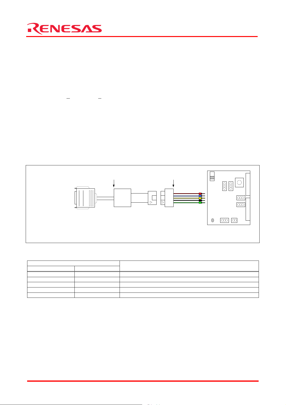
1) Connecting Host PC to Target Board
•Connect D-Sub 9 pin connector of the MF-TEN-NINE cable to COM1 of the host PC.
•Connect MF-TEN-NINE cable to the interface cable.
•Connect IC clip of the interface cable to the target board by referring to Table 4.3.1.
M3S-UFLA32R
MF-TEN-NINE Cable Interface Cable
Connect to
COM1 of the
Host PC
Target Board
Figure 4.3.1 Connection Diagram
Table 4.3.1 Connecting Interface Cable to the Target Board
Interface Cable
IC Clip Color IC Clip Pin Name
Red VCC VCCE power supply
Blue SCLK P87 pin
Yellow RXD P86 pin (RXD1)
Black GND GND pin
Green TXD P85 pin (TXD1)
Destination of the Target Board Connection
2) Setting for FP Pin, MOD0 Pin, and MOD1 Pin
Set FP pin of the target board to "H," MOD0 pin to "H," and MOD1 pin to "L," respectively.
For setting procedure, refer to respective board manuals.
3) Power to the Target Board
Start power supply to the target board.
REJ10B0239-0140/Rev.1.40 Mar. 2007 Page 6 of 30
Page 11

UART Flash Memory Programming Utility
4) Reset the Target MCU
Reset the target MCU by pressing the reset switch on the target board.
5) Starting the M3S-UFLA32R
Start the M3S-UFLA32R.
6) Execution of Writing to the Flash Memory by the M3S-UFLA32R
Operate the M3S-UFLA32R and perform writing to the flash memory.
For detail about operation method, refer to "5. Function Description of the M3S-UFLA32R."
Note: During erasing or writing, it is prohibited to reset the target board and to turn off the power.
7) Exit the M3S-UFLA32R
Exit the M3S-UFLA32R.
8) Power off the Target Board
Cut the power supply to the target board.
M3S-UFLA32R
REJ10B0239-0140/Rev.1.40 Mar. 2007 Page 7 of 30
Page 12
M3S-UFLA32R
UART Flash Memory Programming Utility
5. Function Description of the M3S-UFLA32R
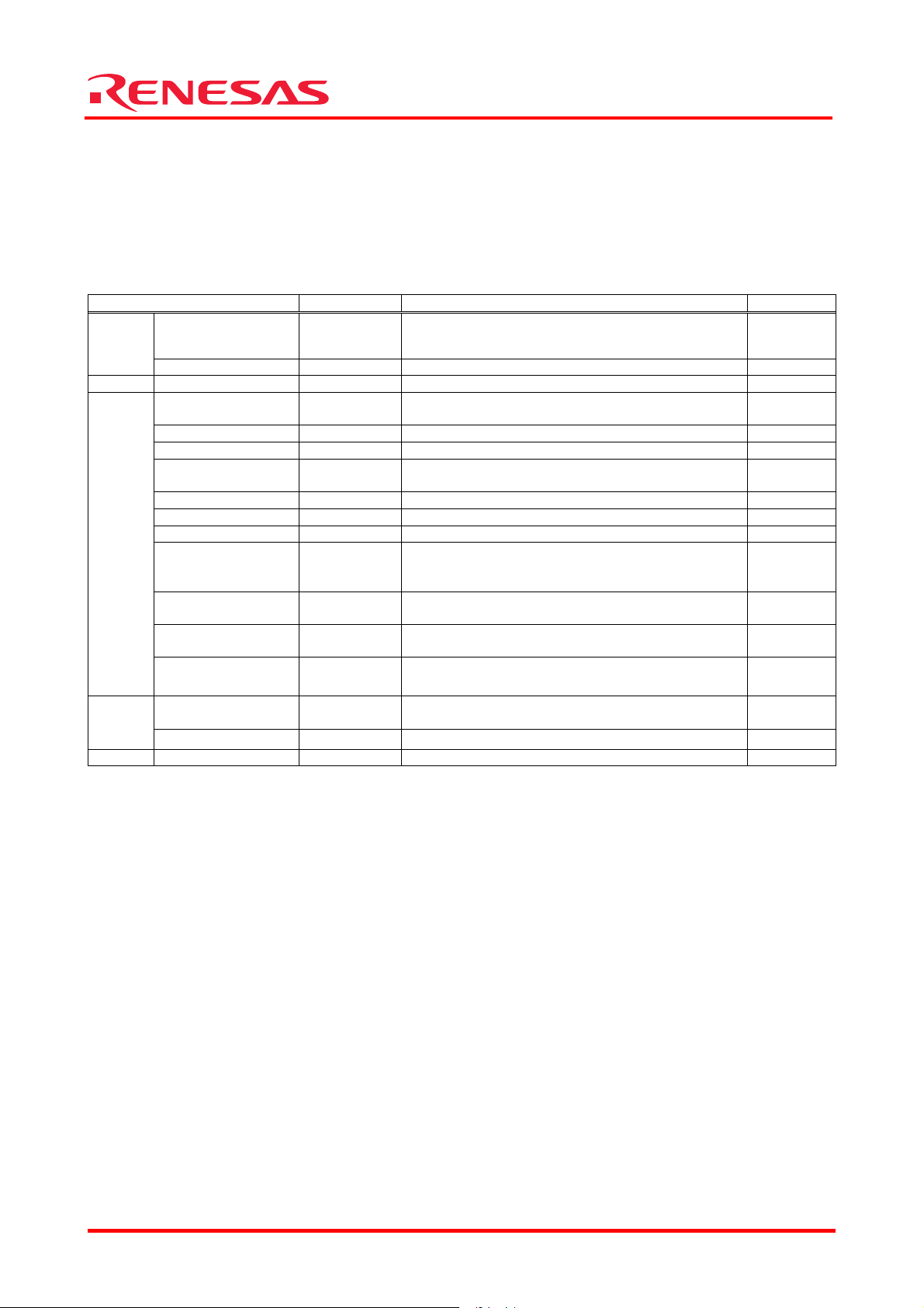
5.1 Function List
Table 5.1 lists functions of the M3S-UFLA32R. Choose each function from menu or click a button
for execution.
Table 5.1 Function List
Menu Button Function Reference
Load Refer Read the program data of specified Motorola S
format file into the internal buffer
Exit - Exit the M3S-UFLA32R 5.3
Display Lock Bit Information - Display lock bit information 5.4
Device
Help Version information - Display the versions of the M3S-UFLA32R and F/W 5.18
Program Program Write program data from internal buffer to the flash
memory
Erase Erase Erase all blocks from the flash memory 5.6
Block Erase - Erase the specified blocks from the flash memory 5.7
Lock Bit / Set - Write lock bit to the specified blocks in the flash
memory
Lock Bit / Enable - Enable memory protect by the lock bit 5.9
Lock Bit / Disable - Disable memory protect by the lock bit 5.10
Blank Check Blank Check Check if all the flash memory blocks are erased 5.11
Verify Check Verify Check Check if the program data of internal buffer and the
program data written to the flash memory are
corresponding
Batch processing
/ E.B.P.V.
Batch processing
/ E.P.
Batch processing
/ B.P.V.
Setting - Perform MCU selection, Verify method selection, and
ID Code Setting
E.B.P.V. Consecutively execute Erase, Blank Check,
Program, and Verify Check
E.P. Consecutively execute Erase and Program 5.14
B.P.V. Consecutively execute Blank Check, Program, and
Verify Check
ID code write control
- Set the ID code to be used at ID verification 5.17
5.2 File
5.5
5.8
5.12
5.13
5.15
5.16 Others
REJ10B0239-0140/Rev.1.40 Mar. 2007 Page 8 of 30
Page 13

M3S-UFLA32R
UART Flash Memory Programming Utility
5.2 Program Data (Motorola S-format file) Selection
(1) Choose [Load(L)] from [File(F)] menu or click [Refer] button.
Figure 5.2.1 Program Data Selection
(2) When “Open File” dialog opens, choose a program data file (Motorola S-format file) and then click
[Open(O
Note: As a file format, the M3S-UFLA32R supports Motorola S-format only.
)] button.
Figure 5.2.2 Open File Dialog
REJ10B0239-0140/Rev.1.40 Mar. 2007 Page 9 of 30
Page 14

M3S-UFLA32R
UART Flash Memory Programming Utility
(3) Choose a file to display the dialog that shows execution process, and then read program data file into
the internal buffer. After completing read, the dialog is closed and file name is displayed in "File
Name:" box.
Figure 5.2.3 Result of Choosing Program Data
5.3 Exit the Application
(1) Choose [Exit(X)] from [File(F)] menu to exit the program.
Also, it is able to exit the program by pushing [Alt + F4] keys or clicking the close button.
Figure 5.3.1 Exit the Application
REJ10B0239-0140/Rev.1.40 Mar. 2007 Page 10 of 30
Page 15
M3S-UFLA32R
UART Flash Memory Programming Utility
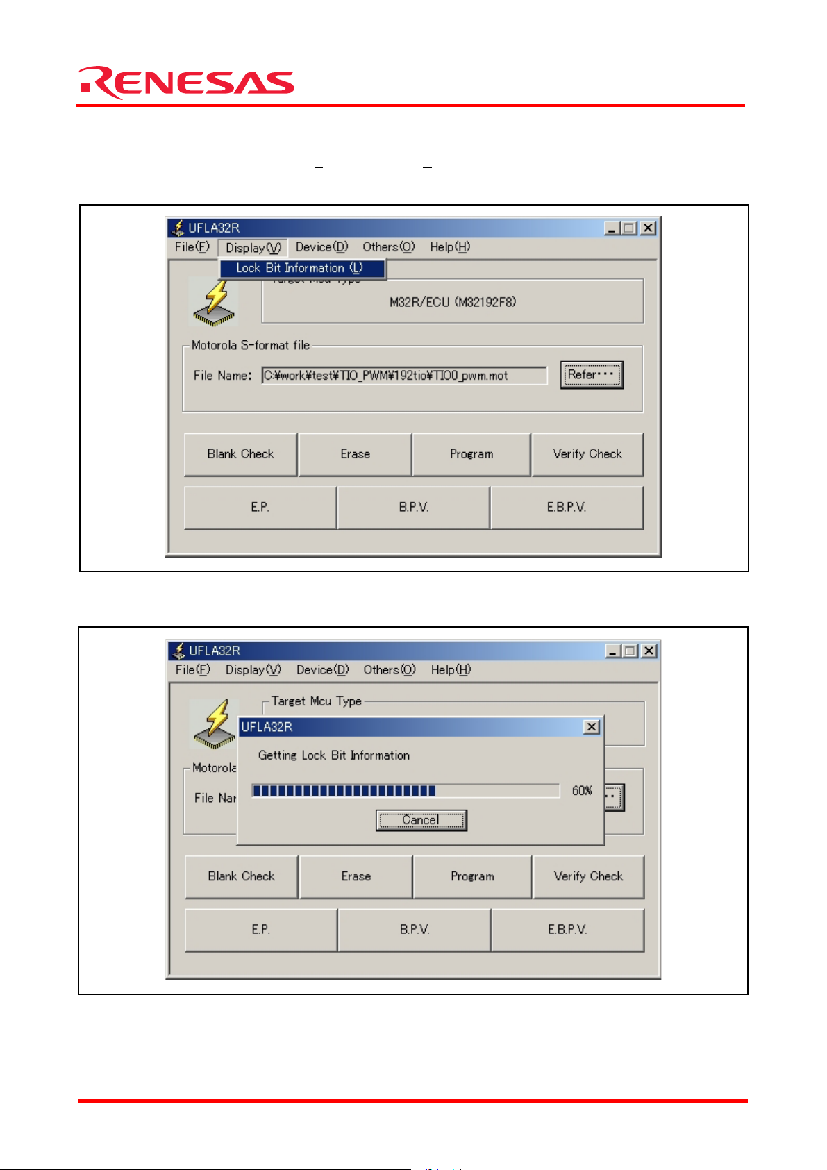
5.4 Lock Bit Information
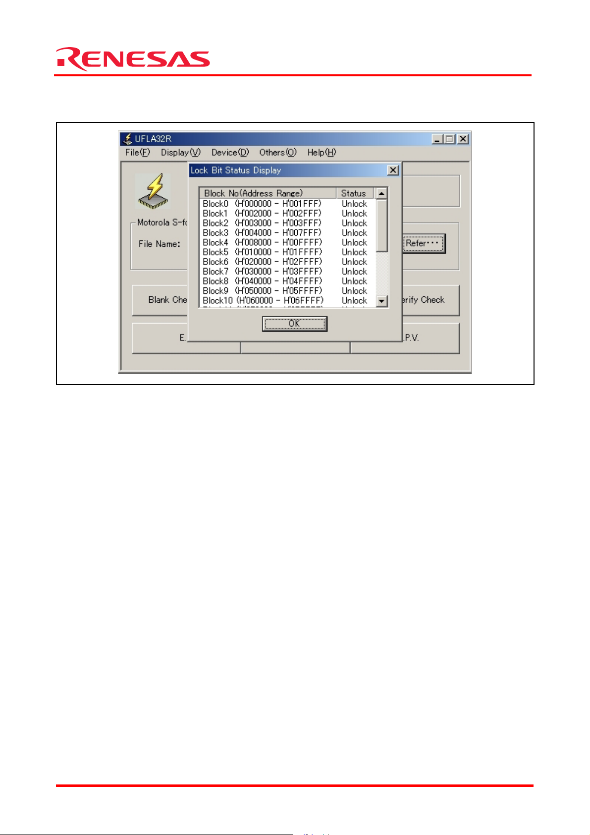
(1) Choose [Lock Bit Information (L)] from [Display(V)] menu to display the dialog that shows execution
process, and then read lock bit. After completing read of lock bit, the dialog is closed and "Lock Bit
Status Display" dialog is displayed.
Figure 5.4.1 Lock Bit Information
(2) Click [Cancel] while reading out lock bit status to close the dialog that shows execution process.
Figure 5.4.2 Reading out Lock Bit Status
REJ10B0239-0140/Rev.1.40 Mar. 2007 Page 11 of 30
Page 16
M3S-UFLA32R
UART Flash Memory Programming Utility
(3) In [Lock Bit Status Display] dialog, the lock bit statuses of all blocks of currently selected MCU are
displayed. Click [OK] to close "Lock Bit Status Display" dialog.
Figure 5.4.3 Lock Bit Status Display Dialog
REJ10B0239-0140/Rev.1.40 Mar. 2007 Page 12 of 30
Page 17
M3S-UFLA32R
UART Flash Memory Programming Utility
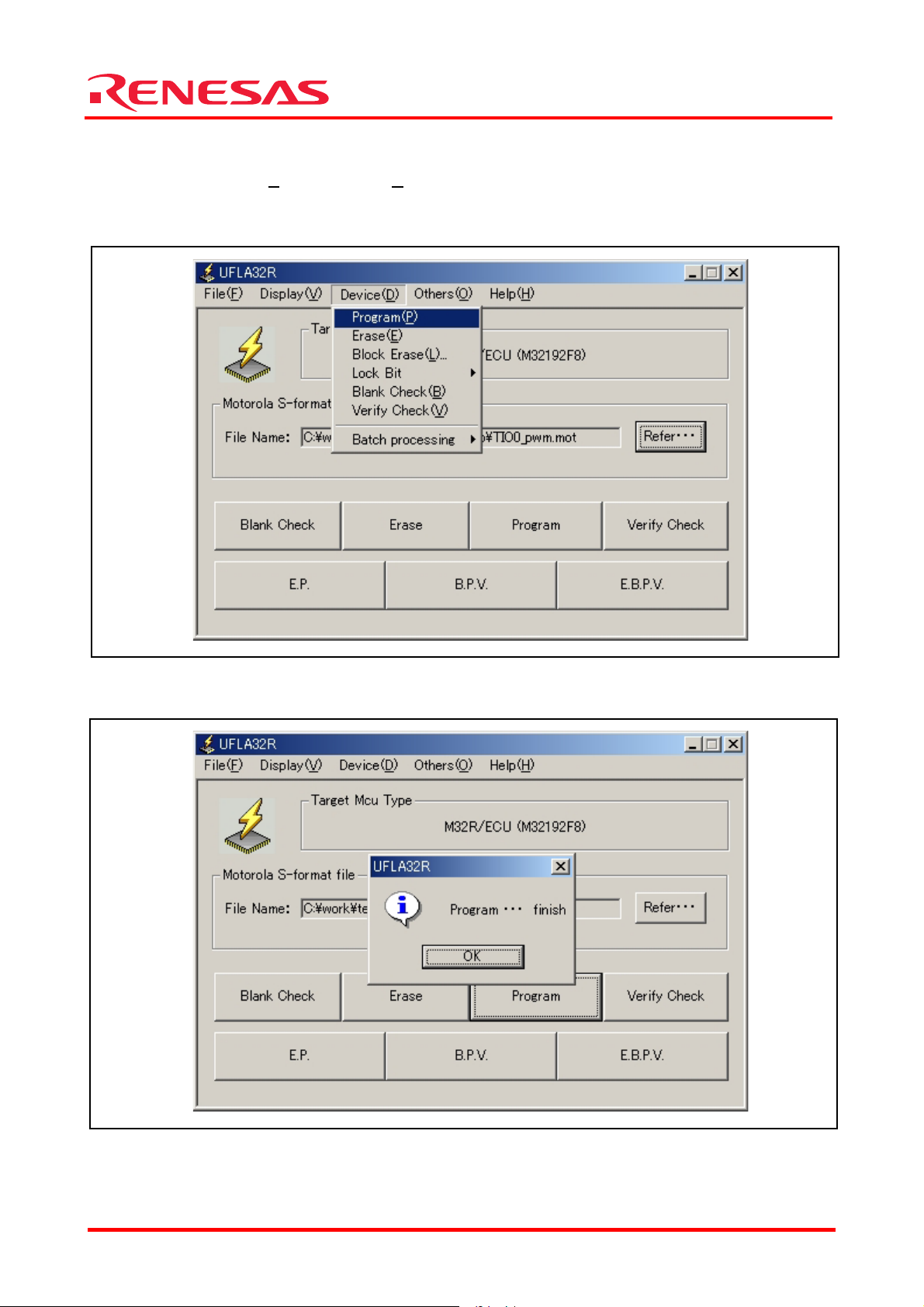
5.5 Program
(1) Choose [Program(P)] from [Device(D)] menu or click [Program] button to display the dialog that
shows execution process, and then write program data stored in the internal buffer to the flash
memory. After completing write of program data, the dialog is closed and "Program …finish" dialog
is displayed.
Figure 5.5.1 Program
(2) Click [OK] in the "Program…finish" dialog to close the dialog
Figure 5.5.2 Program Finish Dialog
REJ10B0239-0140/Rev.1.40 Mar. 2007 Page 13 of 30
Page 18
M3S-UFLA32R
UART Flash Memory Programming Utility
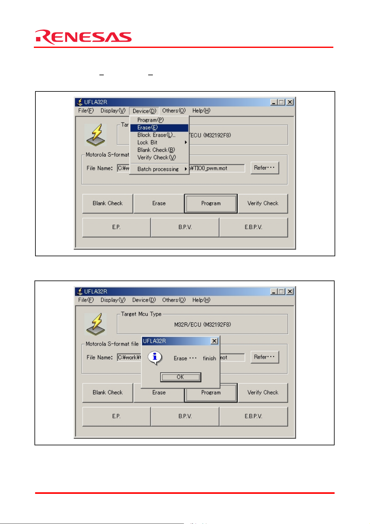
5.6 Erase
(1) Choose [Erase(E)] from [Device(D)] menu or click [Erase] button to display the dialog that shows
execution process, and then erase the flash memory. After completing the flash memory erasing,
the dialog is closed and "Erase …finish" dialog is displayed.
Figure 5.6.1 Erase
(2) Click [OK] in the "Erase…finish" dialog to close the dialog.
Figure 5.6.2 Erase Finish Dialog
REJ10B0239-0140/Rev.1.40 Mar. 2007 Page 14 of 30
Page 19

UART Flash Memory Programming Utility
5.7 Block Erase
(1) Choose [Block Erase(L)] from [Device(D)] menu to display "Block Erase" dialog.
M3S-UFLA32R
Figure 5.7.1 Block Erase
(2) In "Block Erase" dialog, all blocks of currently selected MCU are displayed. Click [Select All] to
select all blocks.
Click [Clear] button to clear all selected blocks.
Select the blocks you wish to erase and click [OK] to close "Block Erase" dialog. Subsequently, the
dialog that shows execution process appears and the selected blocks are erased. After completing
erasing, the dialog is closed and "Block Erase …finish" dialog is displayed. Click [Cancel] to close
"Block Erase" dialog.
Figure 5.7.2 Block Erase Dialog
REJ10B0239-0140/Rev.1.40 Mar. 2007 Page 15 of 30
Page 20
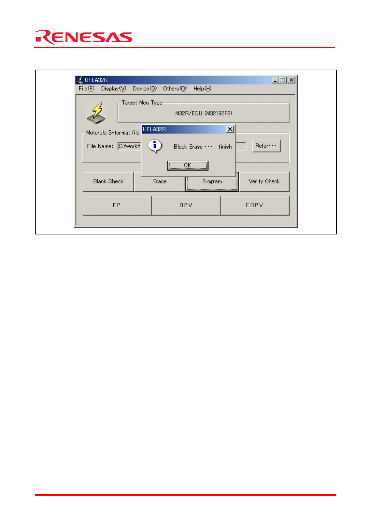
(3) Click [OK] in the "Block Erase…finish" dialog to close the dialog.
M3S-UFLA32R
UART Flash Memory Programming Utility
Figure 5.7.3 Block Erase Finish Dialog
REJ10B0239-0140/Rev.1.40 Mar. 2007 Page 16 of 30
Page 21
M3S-UFLA32R
UART Flash Memory Programming Utility
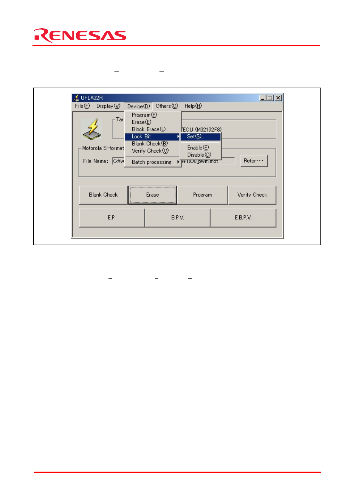
5.8 Lock Bit/Set
(1) Choose [Lock Bit]-[Set(S)] from [Device(D)] menu to display the dialog that shows execution process,
and then read out lock bit. After completing read of lock bit, the dialog is closed and "Lock Bit Set"
dialog is displayed.
Figure 5.8.1 Lock Bit Set
Note: To clear lock bit, perform the following steps.
1. Execute [Lock Bit]-[Disable(D
2. Execute [Erase(E
By following the procedures above, lock bit in the corresponding block can be cleared.
This is the only way to clear lock bit.
)] or [Block Erase(L)] in [Device(D)] menu.
)] in [Device(D)] menu.
REJ10B0239-0140/Rev.1.40 Mar. 2007 Page 17 of 30
Page 22

UART Flash Memory Programming Utility
(2) In "Lock Bit Set" dialog, the blocks without setting of lock bit are displayed.
Click [Select All] to select all blocks.
Click [Clear] to clear all selected blocks.
Select the blocks you wish to set lock bit to, and then click [OK] to close "Lock Bit Set" dialog.
Subsequently, the dialog that shows execution process appears and the lock bit is set. After
completing setting, the dialog is closed and "Lock Bit Set …finish" dialog is displayed.
Click [Cancel] to close "Lock Bit Set" dialog.
M3S-UFLA32R
Figure 5.8.2 Lock Bit Set Dialog
(3) Click [OK] in the "Lock Bit Set…finish" dialog to close the dialog.
Figure 5.8.3 Lock Bit Set Finish Dialog
REJ10B0239-0140/Rev.1.40 Mar. 2007 Page 18 of 30
Page 23

M3S-UFLA32R
UART Flash Memory Programming Utility
5.9 Lock Bit/Enable
(1) Choose [Lock Bit]-[Enable(E)] from [Device(D)] menu to display the dialog that shows execution
process, and then enable lock bit. After completing enabling lock bit, the dialog is closed and "Lock
Bit Enable…finish" dialog is displayed.
Note: It can not perform erase or write operation against the block with the lock bit that is enabled and set.
Clear lock bit to perform erase or write operation.
After powering, lock bit becomes enabled.
Figure 5.9.1 Lock Bit Enable
(2) Click [OK] in the "Lock Bit Enable…finish" dialog to close the dialog.
Figure 5.9.2 Lock Bit Enable Finish Dialog
REJ10B0239-0140/Rev.1.40 Mar. 2007 Page 19 of 30
Page 24

M3S-UFLA32R
UART Flash Memory Programming Utility
5.10 Lock Bit/Disable
(1) Choose [Lock Bit]-[Disable(D)] from [Device(D)] menu to display the dialog that shows execution
process, and then disable lock bit. After completing disabling lock bit, the dialog is closed and "Lock
Bit Disable…finish" dialog is displayed.
Figure 5.10.1 Lock Bit Disable
(2) Click [OK] in the "Lock Bit Disable…finish" dialog to close the dialog.
Figure 5.10.2 Lock Bit Disable Finish Dialog
REJ10B0239-0140/Rev.1.40 Mar. 2007 Page 20 of 30
Page 25

M3S-UFLA32R
UART Flash Memory Programming Utility
5.11 Blank Check
(1) Choose [Blank Check(B)] from [Device(D)] menu or click [Blank Check] button to display the dialog
that shows execution process, and then perform blank check operation. After completing blank
check, the dialog is closed and "Blank Check…finish" dialog is displayed.
Figure 5.11.1 Blank Check
(2) Click [OK] in the "Blank Check…finish" dialog to close the dialog.
Figure 5.11.2 Blank Check Finish Dialog
REJ10B0239-0140/Rev.1.40 Mar. 2007 Page 21 of 30
Page 26

M3S-UFLA32R
UART Flash Memory Programming Utility
5.12 Verify Check
(1) Choose [Verify Check(V)] from [Device(D)] menu or click [Verify Check] button to display the dialog
that shows execution process, and then perform verify check operation. After completing verify
check, the dialog is closed and "Verify Check…finish" dialog is displayed.
Note: When [Sum check (high speed)] is chosen from [Verify Process (V
data in the MCU is compared to the check sum value of the program data file. When [Read array (high
reliability)] is selected, the data in the MCU is compared to the program data file by the byte.
)] in [Others (O)]-[Setting(S)] dialog, the
Figure 5.12.1 Verify Check
(2) Click [OK] in the "Verify Check…finish" dialog box to close the dialog.
Figure 5.12.2 Verify Check Finish Dialog
REJ10B0239-0140/Rev.1.40 Mar. 2007 Page 22 of 30
Page 27
M3S-UFLA32R
UART Flash Memory Programming Utility
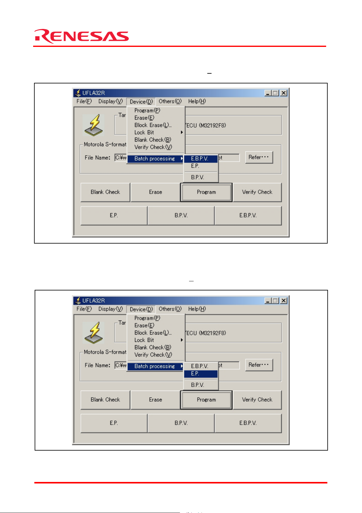
5.13 E.B.P.V. (Erase, Blank Check, Program, Verify Check)
(1) Choose [Batch Processing]-[E.B.P.V.] from [Device(D)] menu or click [E.B.P.V.] button to
consecutively execute "Erase," "Blank Check," "Program," and "Verify Check."
Figure 5.13.1 E.B.P.V.
5.14 E.P. (Erase, Program)
(1) Choose [Batch Processing]-[E.P.] from [Device(D)] menu or click [E.P.] button to consecutively
execute "Erase" and "Program."
Figure 5.14.1 E.P.
REJ10B0239-0140/Rev.1.40 Mar. 2007 Page 23 of 30
Page 28

M3S-UFLA32R
UART Flash Memory Programming Utility
5.15 B.P.V. (Blank Check, Program, Verify Check)
(1) Choose [Batch Processing]-[B.P.V.] from [Device(D)] menu or click [B.P.V.] button to consecutively
execute "Blank Check," "Program," and "Verify Check."
Figure 5.15.1 B.P.V.
REJ10B0239-0140/Rev.1.40 Mar. 2007 Page 24 of 30
Page 29
UART Flash Memory Programming Utility
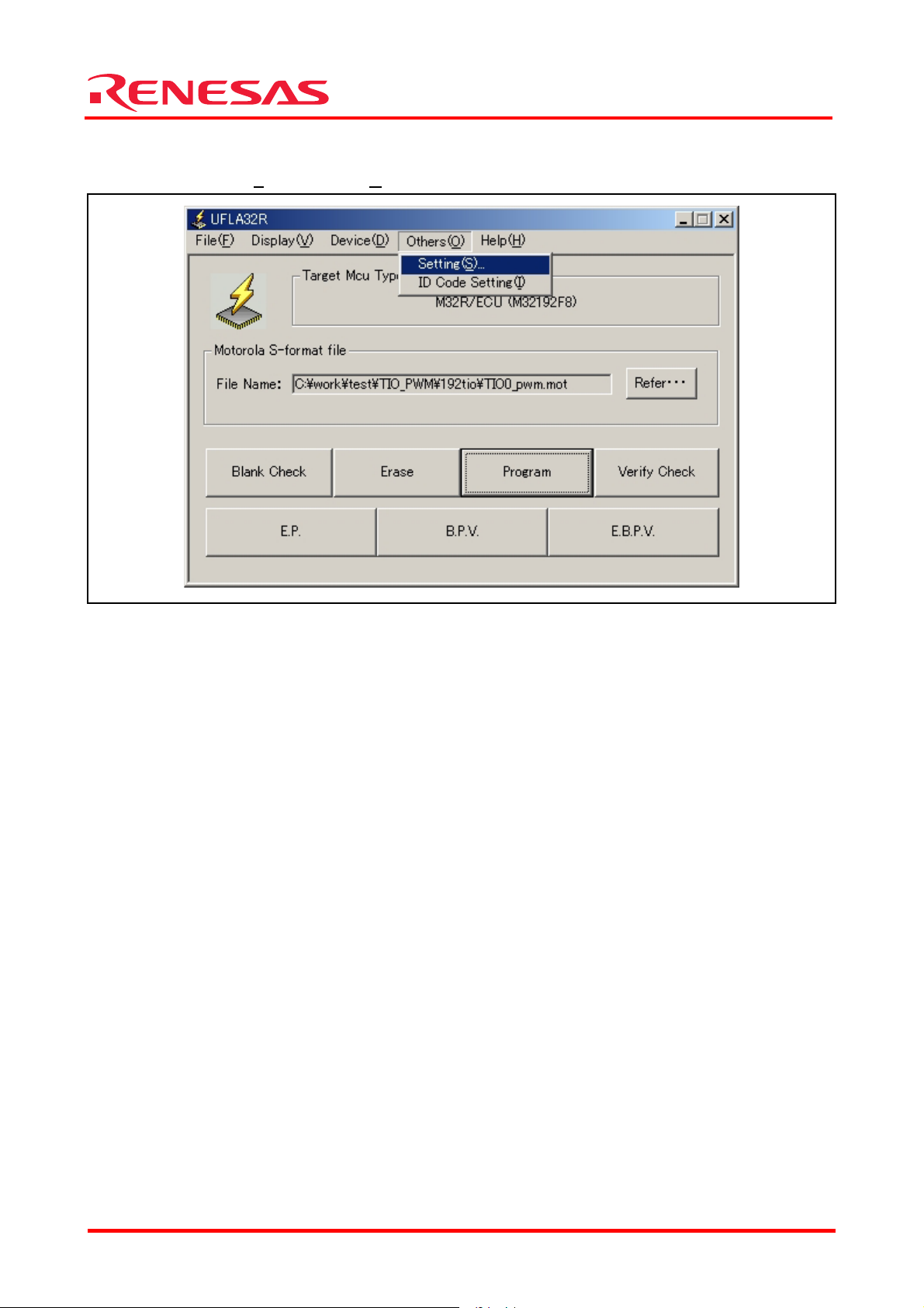
5.16 Setting
(1) Choose [Setting(S)] from [Others(O)] menu to display "Setup" dialog.
M3S-UFLA32R
Figure 5.16.1 Setting
REJ10B0239-0140/Rev.1.40 Mar. 2007 Page 25 of 30
Page 30

M3S-UFLA32R
UART Flash Memory Programming Utility
(2) In the "Setup" dialog, it is possible to choose MCU type, verify process, and write ID code into the ID
code area.
It is possible to choose MCU from "Mcu Type(M
)" pull-down menu.
It is possible to choose verify check process from "Verify process(V)."
Choose [Sum check (high speed)] to compare the data in MCU to the check sum value of the
program data file.
Choose [Read array (high reliability)] to compare the data in MCU to the program data file by the
byte.
Choose [Permit to write ID code into Target MCU] to write data into ID code area of the MCU at the
time of program. If it is not chosen, ID code area of the MCU is filled with FFh.
Write the data other than FFh into ID code area to enable protect function of the flash memory.
When protect function is enabled, the ID code is verified before executing operation to the flash
memory (erase or write). When the ID code is not corresponding as a result of verification, the
operation to the flash memory is not available.
When the whole area of the ID code is filled with FFh, the ID code is not verified.
Note: At the time of the M3S-UFLA32R startup, previously chosen MCU is set to "MCU Type(M)". However,
[Sum check (high speed)] is checked at "Verify process(V
is unchecked.
)" and [Permit to write ID code into Target MCU]
Click [OK] to enable the setting, and then close the "Setup" dialog.
Click [Cancel] to disable the setting, and then close the "Setup" dialog.
Figure 5.16.2 Setup Dialog
REJ10B0239-0140/Rev.1.40 Mar. 2007 Page 26 of 30
Page 31
UART Flash Memory Programming Utility
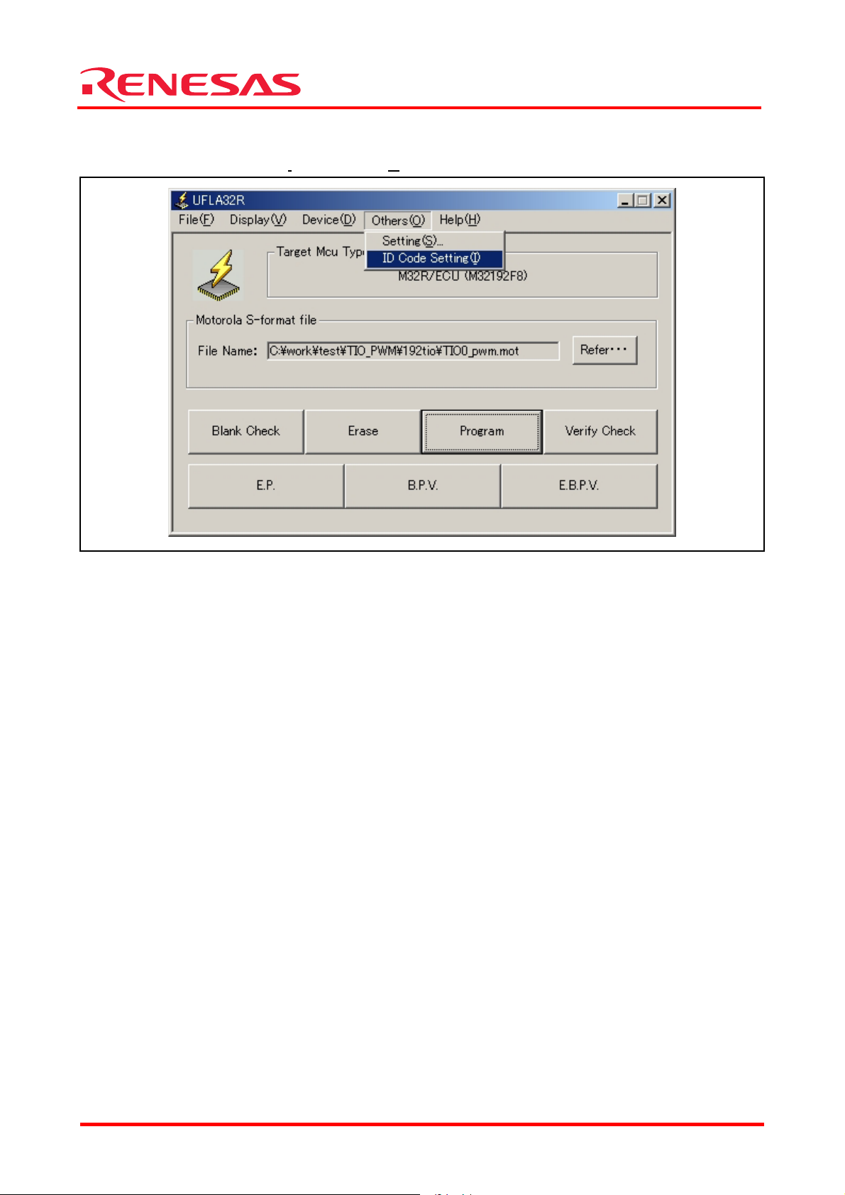
5.17 ID Code Setting
(1) Choose [ID Code Setting(I)] from [Others(O)] menu to display "ID code setting" dialog.
M3S-UFLA32R
Figure 5.17.1 ID Code Setting
REJ10B0239-0140/Rev.1.40 Mar. 2007 Page 27 of 30
Page 32
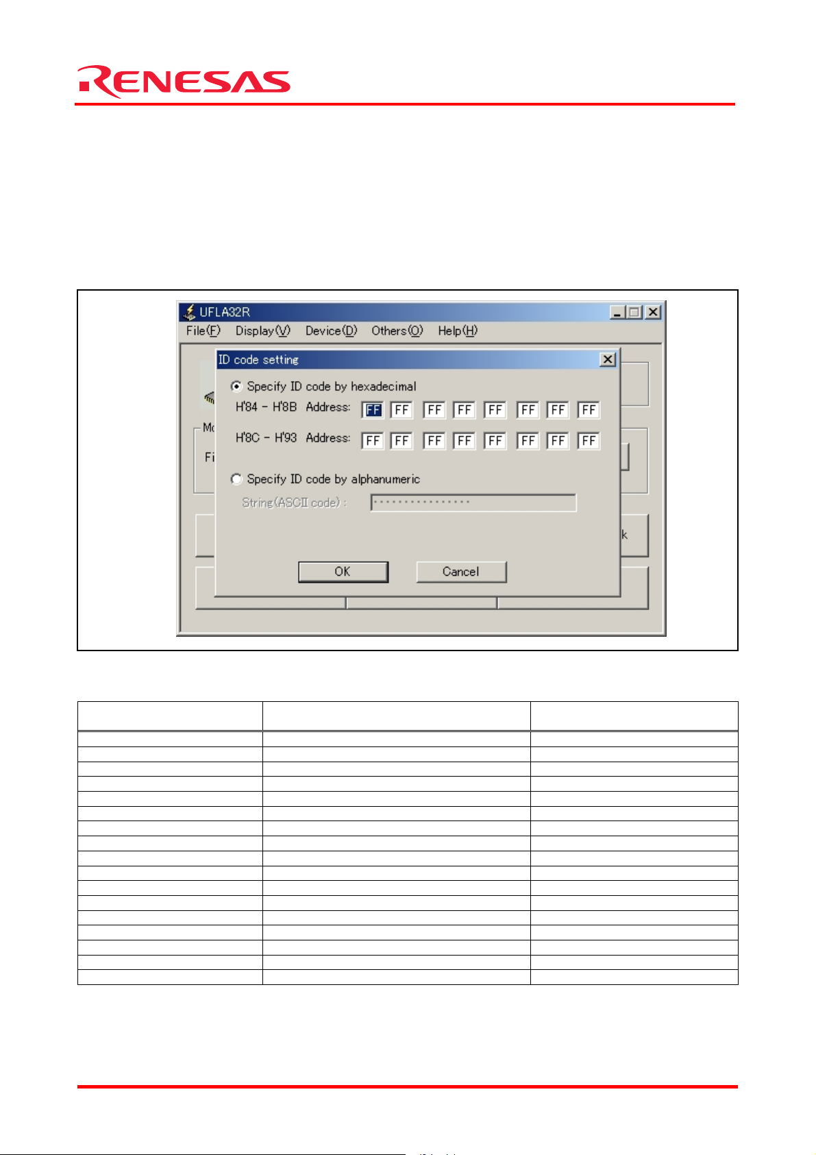
(2) In the "ID code setting" dialog, the ID code for verification is set.
Table 5.17.1 shows function list of operable and not operable functions according with the verify
result.
Choose [Specify ID code by hexadecimal] to set the ID code by hexadecimal.
Choose [Specify ID code by alphanumeric] to set the ID code by alphanumeric characters.
Click [OK] to enable the setting, and then close the "ID code setting" dialog.
Click [Cancel] to disable the setting, and then close the "ID code setting" dialog.
Note: In the 3218x Group and 3219x Group, 12-byte of the address H’84 to H’8F is enabled.
In the other MCU, 16-byte of the address H’84 to H’93 is enabled.
M3S-UFLA32R
UART Flash Memory Programming Utility
Figure 5.17.2 ID Code Setting Dialog
Table 5.17.1 Operable, Not Operable List
Function
Load YES YES
Exit YES YES
Lock Bit Information YES NO
Program YES NO
Erase YES NO
Block Erase YES NO
Lock Bit / Set YES NO
Lock Bit / Enable YES NO
Lock Bit / Disable YES NO
Blank Check YES NO
Verify Check YES NO
Batch processing / E.B.P.V. YES NO
Batch processing / E.P. YES NO
Batch processing / B.P.V. YES NO
Setting YES YES
ID Code Setting YES YES
Version information YES YES
Note: YES: Operable, NO: Not operable
ID code is corresponding or
every ID code in the MCU is FFh
ID code is not corresponding
REJ10B0239-0140/Rev.1.40 Mar. 2007 Page 28 of 30
Page 33

M3S-UFLA32R
UART Flash Memory Programming Utility
5.18 Version Information
(1) Choose [Version information (UFLA32R) (A)] from [Help(H)] menu to display "Version information
(UFLA32R)" dialog.
Figure 5.18.1 Version Information
(2) In the "Version information (UFLA32R)" dialog, the M3S-UFLA32R version and Flash E/W Firmware
version in the MCU are displayed. Click [OK] to close the dialog.
Figure 5.18.2 Version Information (UFLA32R) Dialog
REJ10B0239-0140/Rev.1.40 Mar. 2007 Page 29 of 30
Page 34
M3S-UFLA32R
UART Flash Memory Programming Utility
6. Error Message List
Table 6.1.1 lists error messages, causes, and approaches provided from the M3S-UFLA32R.
Table 6.1.1 Error Message List
Error Message Cause Approach
1 MCU information is incorrect.
Please check whether the "UFLA32R.ini"
file is installed correctly.
2 Can not open COM1. Can not open COM1. Check if the COM1 is used in the
3 Motorola file is not specified.
Please specify Motorola file.
4 The specified file is not a S-format file.
Please specify S-format file (*.mot).
5 Address Error.
Start Address < NNNNNNNNh
6 Address Error.
End Address > NNNNNNNNh
7 Receive timeout error. Timeout occurs during reception. Check the connection state of the
8 Communication parameter error. Receive reply other than ACK
9 Command execution error. Receive NAK from the MCU. Restart the M3S-UFLA32R and
10 Blank Check Error.
(Error Address: H'NNNNNN)
11 Verify Check Error.
Error Address : H'NNNNNN
Error Data : H'AAAA (H'BBBB)
12 Verify Check Error. Check sum value is not
13 ID verification error.
Please set up the ID code correctly.
14 ID code is incorrect.
Please enter ID code with Hexadecimal.
15 ID code is incorrect.
Please enter ID code correctly.
There is no INI file. Reinstall the M3S-UFLA32R.
other application.
Motorola S format file is not
specified.
The specified file is not Motorola
S-format file or there are some
contents errors.
The data record address of
chosen file is beyond the flash
memory.
The record length of the chosen
file has an error.
and NAK from the MCU.
There is no blank after the
address H’NNNNNN.
At the time of verify, the data of
the address H’NNNNNN are
H’AAAA (MCU side) and H’BBBB
(M3S-UFLA32R side) and not
corresponding.
corresponding at the time of
verification
The ID code in the MCU and the
one set in the M3S-UFLA32R
are different
Input ID code has an error. Enter ID code with Hexadecimal.
Input ID code has an error. Enter ID code with alphanumeric
Specify the Motorola S format file.
Check the contents of the
selected file or specify different
file.
Check the contents of Motorola S
format file or specify different file.
Check the contents of Motorola S
format file or specify different file.
communication cable or restart
the M3S-UFLA32R, and then
reset the MCU.
Restart the M3S-UFLA32R and
reset the MCU.
reset the MCU.
-
Check if it is the same Motorola S
format file as the program in the
MCU.
Check if it is the same Motorola S
format file as the program in the
MCU.
Set the correct ID code to the
M3S-UFLA32R.
characters.
REJ10B0239-0140/Rev.1.40 Mar. 2007 Page 30 of 30
Page 35
Revision History
M3S-UFLA32R
UART Flash Memory Programming Utility
Rev. Date
1.00 Jun 25, 2000 - First edition issued.
1.01 Dec 4, 2000 - Changed output message from Japanese to English.
1.02 Jan 29, 2002 7
1.03 Feb 14, 2002 7
1.04 Mar 1, 2002 2
1.10 Oct 28, 2002 6
1.20 Dec 3, 2002 6
1.30 Jul 11, 2003 -
1.40 Mar 6, 2007 -
Page Summary
Added references to 2) Connecting Host PC with Target System in
Chapter 3.
Changed product name from UFLA32 to M3A-UFLA32R.
Changed the description of 2) Connecting Host PC with Target System
in Chapter 3.
Added "Notes regarding these materials."
Added description to 1) Setting up M3S-UFLA32R in Chapter 3.
Changed the location where "Setup.exe" is stored in a CD-ROM.
Changed the layout of window.
Supported 32176/32180/32182 Group MCUs.
Supported 32185/32186 Group and 32192/32195/32196 Group MCUs.
Reviewed overall contents.
Description
Page 36

Uart Flash Memory Programming Utility
User’s Manual
M3S-UFLA32R
Publication Date: 1st Edition, Jun., 2000
Rev.1.40, Mar. 06, 2007
Published by: Sales Strategic Planning Div.
Renesas Technology Corp.
2007. Renesas Technology Corp., All rights reserved. Printed in Japan.
Page 37

M3S-UFLA32R
User’s Manual
2-6-2, Ote-machi, Chiyoda-ku, Tokyo, 100-0004, Japan
 Loading...