

Page 1
M37549T-RLSS
Emulator MCU Board for 7548/7549 Group
User’s Manual
CAUTION
Renesas Tools Homepage http://www.renesas.com/tools
Rev.1.00
Jul. 10, 2007
REJ10J1444-0100
If the requirements shown in the "CAUTION" sentences are ignored,
the equipment may cause personal injury or damage to the products.
(1/4)
Page 2
1. Outline
The M37549T-RLSS is an emulator MCU board for the 7548/7549 Group.
2. Package Components
(1) M37549T-RLSS 1 pc.
(2) M37549T-RLSS User's Manual (This manual) 1 pc.
(3) M37549T-RLSS User's Manual (Japanese) 1 pc.
3. Specifications
1 Specifications
Table
Emulator M38000T2-CPE *
Operating mode Single-chip mode
Vcc = 4.5 to 5.0 V: 8.0 MHz (frequency/2 mode)
Vcc = 2.4 to 5.0 V: 2.0 MHz (frequency/2 mode)
Maximum operating
frequency
Operating power
voltage
Vcc = 2.2 to 5.0 V: 1.0 MHz (frequency/2 mode)
Vcc = 4.0 to 5.0 V: 8.0 MHz (High-speed mode)
Vcc = 2.4 to 5.0 V: 4.0 MHz (High-speed mode)
Vcc = 1.8 to 5.0 V: 1.0 MHz (High-speed mode)
1.8 to 5.5 V
* A combination of the PC4701 and M38000TL2-FPD is not supported.
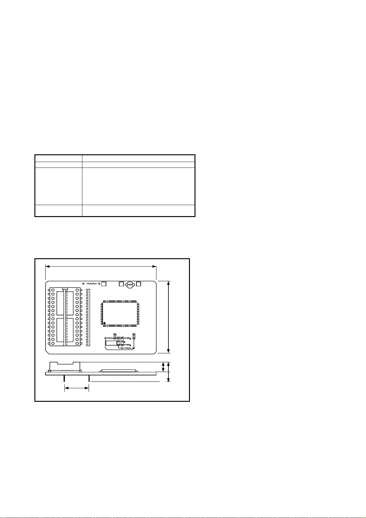
4. External Dimensions
64.0
R1
15. 24
Figure 1 External dimensions
VCCGNDRESET
+
45.0
11.0
4.2
(2/4)
Page 3

5. Connection Procedure to the user system
Connect the emulation probe to the connector on the upper panel of the M37549T-RLSS. Connect the M37549T-RLSS to the 42-pin
SDIP socket on the user system. Table 2 shows pin allocation of the M37549T-RLSS, and Figure 2 shows connector dimensions.
Table 2 CN1 connector pin allocation
Pin No Signal Pin No Signal
1 N.C 42 N.C
2 N.C 41 N.C
3 N.C 40 P13/AN3/KEY3
4 P14/AN4/KEY4 39 P12/AN2/CMP2
5 P15/AN5/KEY5 38 P11/AN1/CMP1
6 RESET 37 P10/AN0/CMP0
7 P16/AN6/KEY6 36 P31
8 P17/AN7/KEY7 35 P30
9 N.C 34 Reserved
10 N.C 33 Reserved
11 N.C 32 Reserved
12 P20/Xout/Xcout 31 Reserved
13 Vss 30 P07(LED7)/Srdy
14 P21/Xin/Xcin 29 P06(LED6)/Sclk
15 Vcc 28 P05(LED5)/TxD
16 CNVss 27 P04(LED4)/RxD
17 P00(LED0)/INT0 26 P03(LED3)/CAP0
18 P01(LED1)/INT1 25 P02(LED2)
19 N.C 24 N.C
20 N.C 23 N.C
21 Vss 22 N.C
* Do not connect signal to Reserved parts.
15.24
1 42
1.778
21 22
Figure 2 CN connector dimensions
(3/4)
Page 4

6. Oscillator Circuit
This product has two oscillator circuit patterns for the main clock XIN and sub-clock XCIN. The oscillator circuit on the user system
may not work properly because the oscillator circuit pin of the emulator MCU is not close enough to the oscillator circuit of the user
system. In this case, mount the oscillator circuit on the oscillator circuit pattern of the M37549T-RLSS.
Figures 3, 4 and 5 show the M37549T-RLSS circuit pattern and diagram.
JP2 JP3
xin
X2b
X2a
R2
C1
xout
JP2
JP3
X1
C2
R3
RdX2
X2
C1 C2
R3
Figure 3 When a ceramic oscillator with built-in capacitor is used for Xin/Xout
X2a
Capacitor
C1
C2
R3
xout
JP2
X2
C1 C2
JP3
R3
JP2 JP3
xin
R2
X2
X2b
X1
Rd
Figure 4 When a ceramic oscillator without built-in capacitor is used for Xin/Xout
Rf
JP2 JP3
xin
R2
X2
X2b
X1
Rd
Capacitor
X2a
C1
C2
xout
R3
JP2
R2
X1
C1 C2
JP3
R3
Figure 5 When Xcin/Xcout is used as a circuit
7. Precautions
Notes on This Product:
z We cannot accept any request for repair.
z When using the oscillator circuit on the M37549T-RLSS, check output waveform of pin Xout and pin Xcout with an
oscilloscope.
z When mounting an oscillator circuit on the M37549T-RLSS, make sure not to short-circuit the user system.
z For inquiries about the product or the contents of this manual, contact your local distributor.
Renesas Tools Homepage http://www.renesas.com/tools
IMPORTANT
(4/4)
 Loading...