

Page 1

OCO
R
S
REJ09B0202-0200
16
M16C/26A Group
(M16C/26A, M16C/26B, M16C/26T)
Hardware Manual
RENESAS 16-BIT SINGLE-CHIP MICR
M16C FAMILY / M16C/T iny SERIE
MPUTE
All information contained in these materials, including products and product specifications,
represents information on the product at the time of publication and is subject to change by
Renesas Technology Corp. without notice. Please review the latest information published
by Renesas Technology Corp. through various means, including the Renesas Technology
Corp. website (http://www.renesas.com).
Rev. 2.00
Revision Date: Feb.15, 2007
www.renesas.com
Page 2

Notes regarding these materials
1. This document is provided for reference purposes only so that Renesas customers may select the appropriate
Renesas products for their use. Renesas neither makes warranties or representations with respect to the
accuracy or completeness of the information contained in this document nor grants any license to any
intellectual property rights or any other rights of Renesas or any third party with respect to the information in
this document.
2. Renesas shall have no liability for damages or infringement of any intellectual property or other rights arising
out of the use of any information in this document, including, but not limited to, product data, diagrams, charts,
programs, algorithms, and application circuit examples.
3. You should not use the products or the technology described in this document for the purpose of military
applications such as the development of weapons of mass destruction or for the purpose of any other military
use. When exporting the products or technology described herein, you should follow the applicable export
control laws and regulations, and procedures required by such laws and regulations.
4. All information included in this document such as product data, diagrams, charts, programs, algorithms, and
application circuit examples, is current as of the date this document is issued. Such information, however, is
subject to change without any prior notice. Before purchasing or using any Renesas products listed in this
document, please confirm the latest product information with a Renesas sales office. Also, please pay regular
and careful attention to additional and different information to be disclosed by Renesas such as that disclosed
through our website. (http://www.renesas.com )
5. Renesas has used reasonable care in compiling the information included in this document, but Renesas
assumes no liability whatsoever for any damages incurred as a result of errors or omissions in the information
included in this document.
6. When using or otherwise relying on the information in this document, you should evaluate the information in
light of the total system before deciding about the applicability of such information to the intended application.
Renesas makes no representations, warranties or guaranties regarding the suitability of its products for any
particular application and specifically disclaims any liability arising out of the application and use of the
information in this document or Renesas products.
7. With the exception of products specified by Renesas as suitable for automobile applications, Renesas
products are not designed, manufactured or tested for applications or otherwise in systems the failure or
malfunction of which may cause a direct threat to human life or create a risk of human injury or which require
especially high quality and reliability such as safety systems, or equipment or systems for transportation and
traffic, healthcare, combustion control, aerospace and aeronautics, nuclear power, or undersea communication
transmission. If you are considering the use of our products for such purposes, please contact a Renesas
sales office beforehand. Renesas shall have no liability for damages arising out of the uses set forth above.
8. Notwithstanding the preceding paragraph, you should not use Renesas products for the purposes listed below:
(1) artificial life support devices or systems
(2) surgical implantations
(3) healthcare intervention (e.g., excision, administration of medication, etc.)
(4) any other purposes that pose a direct threat to human life
Renesas shall have no liability for damages arising out of the uses set forth in the above and purchasers who
elect to use Renesas products in any of the foregoing applications shall indemnify and hold harmless Renesas
Technology Corp., its affiliated companies and their officers, directors, and employees against any and all
damages arising out of such applications.
9. You should use the products described herein within the range specified by Renesas, especially with respect
to the maximum rating, operating supply voltage range, movement power voltage range, heat radiation
characteristics, installation and other product characteristics. Renesas shall have no liability for malfunctions or
damages arising out of the use of Renesas products beyond such specified ranges.
10. Although Renesas endeavors to improve the quality and reliability of its products, IC products have specific
characteristics such as the occurrence of failure at a certain rate and malfunctions under certain use
conditions. Please be sure to implement safety measures to guard against the possibility of physical injury, and
injury or damage caused by fire in the event of the failure of a Renesas product, such as safety design for
hardware and software including but not limited to redundancy, fire control and malfunction prevention,
appropriate treatment for aging degradation or any other applicable measures. Among others, since the
evaluation of microcomputer software alone is very difficult, please evaluate the safety of the final products or
system manufactured by you.
11. In case Renesas products listed in this document are detached from the products to which the Renesas
products are attached or affixed, the risk of accident such as swallowing by infants and small children is very
high. You should implement safety measures so that Renesas products may not be easily detached from your
products. Renesas shall have no liability for damages arising out of such detachment.
12. This document may not be reproduced or duplicated, in any form, in whole or in part, without prior written
approval from Renesas.
13. Please contact a Renesas sales office if you have any questions regarding the information contained in this
document, Renesas semiconductor products, or if you have any other inquiries.
Page 3

General Precautions in the Handling of MPU/MCU Products
The following usage notes are applicable to all MPU/MCU products from Renesas. For detailed usage notes
on the products covered by this manual, refer to the relevant sections of the manual. If the descriptions under
General Precautions in the Handling of MPU/MCU Products and in the body of the manual differ from each
other, the description in the body of the manual takes precedence.
1. Handling of Unused Pins
Handle unused pins in accord with the directions given under Handling of Unused Pins in the
manual.
The input pins of CMOS products are generally in the high-impedance state. In operation
with an unused pin in the open-circuit state, extra electromagnetic noise is induced in the
vicinity of LSI, an associated shoot-through current flows internally, and malfunctions occur
due to the false recognition of the pin state as an input signal become possible. Unused
pins should be handled as described under Handling of Unused Pins in the manual.
2. Processing at Power-on
The state of the product is undefined at the moment when power is supplied.
The states of internal circuits in the LSI are indeterminate and the states of register
settings and pins are undefined at the moment when power is supplied.
In a finished product where the reset signal is applied to the external reset pin, the states
of pins are not guaranteed from the moment when power is supplied until the reset
process is completed.
In a similar way, the states of pins in a product that is reset by an on-chip power-on reset
function are not guaranteed from the moment when power is supplied until the power
reaches the level at which resetting has been specified.
3. Prohibition of Access to Reserved Addresses
Access to reserved addresses is prohibited.
The reserved addresses are provided for the possible future expansion of functions. Do
not access these addresses; the correct operation of LSI is not guaranteed if they are
accessed.
4. Clock Signals
After applying a reset, only release the reset line after the operating clock signal has become
stable. When switching the clock signal during program execution, wait until the target clock
signal has stabilized.
When the clock signal is generated with an external resonator (or from an external
oscillator) during a reset, ensure that the reset line is only released after full stabilization of
the clock signal. Moreover, when switching to a clock signal produced with an external
resonator (or by an external oscillator) while program execution is in progress, wait until
the target clock signal is stable.
5. Differences between Products
Before changing from one product to another, i.e. to one with a different part number, confirm
that the change will not lead to problems.
The characteristics of MPU/MCU in the same group but having different part numbers may
differ because of the differences in internal memory capacity and layout pattern. When
changing to products of different part numbers, implement a system-evaluation test for
each of the products.
Page 4

How to Use This Manual
1. Purpose and Target Readers
This manual is designed to provide the user with an understanding of the hardware functions and electrical
characteristics of the MCU. It is intended for users designing application systems incorporating the MCU. A basic
knowledge of electric circuits, logical circuits, and MCUs is necessary in order to use this manual.
The manual comprises an overview of the product; descriptions of the CPU, system control functions, peripheral
functions, and electrical characteristics; and usage notes.
Particular attention should be paid to the precautionary notes when using the manual. These notes occur
within the body of the text, at the end of each section, and in the Usage Notes section.
The revision history summarizes the locations of revisions and additions. It does not list all revisions. Refer
to the text of the manual for details.
The following documents apply to the M16C/26A Group (M16C/26A, M16C/26B, and M16C/26T). Make sure to
refer to the latest versions of these documents. The newest versions of the documents listed may be obtained from the
Renesas Technology Web site.
Document Type Description Document Title Document No.
Hardware manual Hardware specifications (pin assignments,
memory maps, peripheral function
specifications, electrical characteristics, timing
charts) and operation description
Note: Refer to the application notes for details on
using peripheral functions.
Software manual Description of CPU instruction set M16C/60,
Application note Information on using peripheral functions and
application examples
Sample programs
Information on writing programs in assembly
language and C
Renesas
technical update
Product specifications, updates on documents,
etc.
M16C/26A Group
(M16C/26A,
M16C/26B,
M16C/26T)
Hardware Manual
M16C/20,
M16C/Tiny Series
Software Manual
Available from Renesas
Technology Web site.
This hardware
manual
REJ09B0137
Page 5

2. Notation of Numbers and Symbols
The notation conventions for register names, bit names, numbers, and symbols used in this manual are described
below.
(1) Register Names, Bit Names, and Pin Names
Registers, bits, and pins are referred to in the text by symbols. The symbol is accompanied by the word
“register,” “bit,” or “pin” to distinguish the three categories.
Examples the PM03 bit in the PM0 register
P3_5 pin, VCC pin
(2) Notation of Numbers
The indication “
values of single bits. The indication “
is appended to numeric values given in decimal format.
Examples Binary: 11
2” is appended to numeric values given in binary format. However, nothing is appended to the
16” is appended to numeric values given in hexadecimal format. Nothing
2
Hexadecimal: EFA016
Decimal: 1234
Page 6
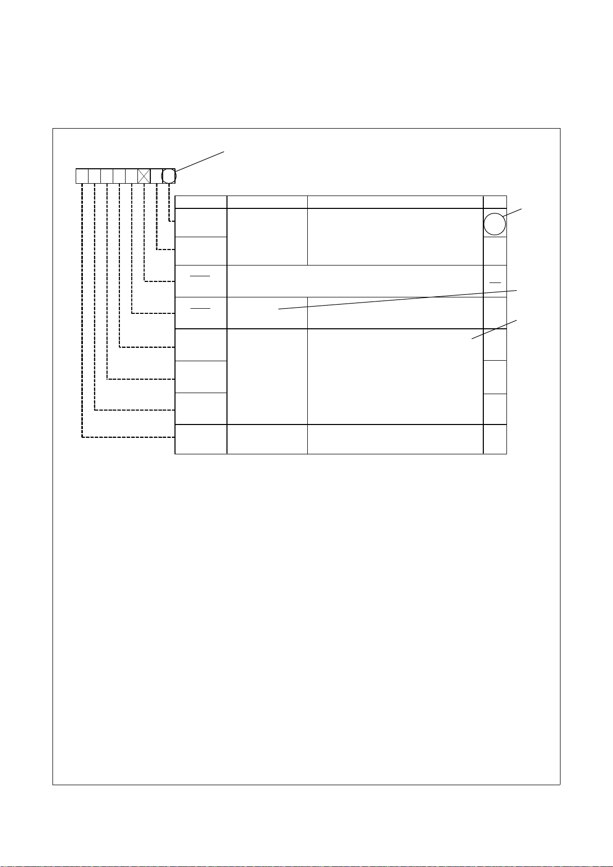
3. Register Notation
The symbols and terms used in register diagrams are described below.
XXX Register
b7 b6 b5 b4 b3 b2 b1 b0
0
XXX0
XXX1
(b2)
(b3)
XXX4
XXX5
XXX6
XXX7
*1
Symbol Address After Reset
XXX XXX 00
Bit NameBit Symbol
XXX bits
Nothing is assigned. If necessary, set to 0.
When read, the content is undefined.
Reserved bits
XXX bits
XXX bit
b1 b0
1 0: XXX
0 1: XXX
1 0: Do not set.
1 1: XXX
Set to 0.
Function varies according to the operating
mode.
0: XXX
1: XXX
Function
16
RW
RW
RW
*2
*3
RW
*4
RW
WO
RW
RO
*1
Blank: Set to 0 or 1 according to the application.
0: Set to 0.
1: Set to 1.
X: Nothing is assigned.
*2
RW: Read and write.
RO: Read only.
WO: Write only.
−: Nothing is assigned.
*3
• Reserved bit
Reserved bit. Set to specified value.
*4
• Nothing is assigned
Nothing is assigned to the bit. As the bit may be used for future functions, if necessary, set to 0.
• Do not set to a value
Operation is not guaranteed when a value is set.
• Function varies according to the operating mode.
The function of the bit varies with the peripheral function mode. Refer to the register diagram for information
on the individual modes.
Page 7

4. List of Abbreviations and Acronyms
Abbreviation Full Form
ACIA Asynchronous Communication Interface Adapter
bps bits per second
CRC Cyclic Redundancy Check
DMA Direct Memory Access
DMAC Direct Memory Access Controller
GSM Global System for Mobile Communications
Hi-Z High Impedance
IEBus Inter Equipment bus
I/O Input/Output
IrDA Infrared Data Association
LSB Least Significant Bit
MSB Most Significant Bit
NC Non-Connection
PLL Phase Locked Loop
PWM Pulse Width Modulation
SFR Special Function Registers
SIM Subscriber Identity Module
UART Universal Asynchronous Receiver/Transmitter
VCO Voltage Controlled Oscillator
All trademarks and registered trademarks are the property of their respective owners.
IEBus is a registered trademark of NEC Electronics Corporation.
Page 8

Table of Contents
Quick Reference by Address_______________________ B-1
1. Overview ______________________________________ 1
1.1 Applications ...................................................................................................................1
1.2 Performance Outline .....................................................................................................2
1.3 Block Diagram...............................................................................................................4
1.4 Product List ...................................................................................................................6
1.5 Pin Assignments..........................................................................................................11
1.6 Pin Description ............................................................................................................15
2. Central Processing Unit (CPU) ____________________ 17
2.1 Data Registers (R0, R1, R2 and R3)...........................................................................17
2.2 Address Registers (A0 and A1)...................................................................................17
2.3 Frame Base Register (FB) ..........................................................................................18
2.4 Interrupt Table Register (INTB) ...................................................................................18
2.5 Program Counter (PC) ................................................................................................18
2.6 User Stack Pointer (USP) and Interrupt Stack Pointer (ISP) ......................................18
2.7 Static Base Register (SB) ...........................................................................................18
2.8 Flag Register (FLG) ....................................................................................................18
2.8.1 Carry Flag (C Flag) ..............................................................................................18
2.8.2 Debug Flag (D Flag) ............................................................................................18
2.8.3 Zero Flag (Z Flag) ...............................................................................................18
2.8.4 Sign Flag (S Flag) ................................................................................................18
2.8.5 Register Bank Select Flag (B Flag)...................................................................... 18
2.8.6 Overflow Flag (O Flag).........................................................................................18
2.8.7 Interrupt Enable Flag (I Flag) ...............................................................................18
2.8.8 Stack Pointer Select Flag (U Flag)....................................................................... 18
2.8.9 Processor Interrupt Priority Level (IPL)................................................................18
2.8.10 Reserved Area ...................................................................................................18
3. Memory ______________________________________ 19
4. Special Function Registers (SFRs) _________________ 20
A-1
Page 9

5. Reset________________________________________ 26
5.1 Hardware Reset ..........................................................................................................26
5.1.1 Hardware Reset 1 ................................................................................................26
5.1.2 Hardware Reset 2 ................................................................................................26
5.2 Software Reset............................................................................................................27
5.3 Watchdog Timer Reset................................................................................................27
5.4 Oscillation Stop Detection Reset.................................................................................27
5.5 Voltage Detection Circuit.............................................................................................29
5.5.1 Voltage Down Detection Interrupt .......................................................................32
5.5.2 Limitations on Exiting Stop Mode........................................................................ 34
5.5.3 Limitations on Exiting Wait Mode........................................................................34
6. Processor Mode _______________________________ 35
7. Clock Generation Circuit _________________________ 38
7.1 Main Clock ..................................................................................................................45
7.2 Sub Clock....................................................................................................................46
7.3 On-chip Oscillator Clock..............................................................................................47
7.4 PLL Clock ....................................................................................................................47
7.5 CPU Clock and Peripheral Function Clock .................................................................49
7.5.1 CPU Clock ...........................................................................................................49
7.5.2 Peripheral Function Clock (f1, f2, f8, f32, f1SIO, f2SIO, f8SIO, f32SIO, fAD, fC32) .......49
7.5.3 ClockOutput Function ..........................................................................................49
7.6 Power Control .............................................................................................................50
7.6.1 Normal Operation Mode.......................................................................................50
7.6.2 Wait Mode............................................................................................................51
7.6.3 Stop Mode...........................................................................................................53
7.7 System Clock Protective Function ..............................................................................57
7.8 Oscillation Stop and Re-oscillation Detect Function ...................................................57
7.8.1 Operation When the CM27 bit is set to "0" (Oscillation Stop Detection Reset) ...58
7.8.2 Operation When the CM27 bit is set to "1"
(Oscillation Stop and Re-oscillation Detect Interrupt) ..................58
7.8.3 How to Use Oscillation Stop and Re-oscillation Detect Function......................... 59
8. Protection ____________________________________ 60
9. Interrupt______________________________________ 61
9.1 Type of Interrupts ........................................................................................................61
9.1.1 Software Interrupts...............................................................................................62
9.1.2 Hardware Interrupts .............................................................................................63
A-2
Page 10

9.2 Interrupts and Interrupt Vector ....................................................................................64
9.2.1 Fixed Vector Tables..............................................................................................64
9.2.2 Relocatable Vector Tables ...................................................................................65
9.3 Interrupt Control ..........................................................................................................66
9.3.1 I Flag ....................................................................................................................69
9.3.2 IR Bit ....................................................................................................................69
9.3.3 ILVL2 to ILVL0 Bits and IPL .................................................................................69
9.4 Interrupt Sequence......................................................................................................70
9.4.1 Interrupt Response Time......................................................................................71
9.4.2 Variation of IPL when Interrupt Request is Accepted...........................................71
9.4.3 Saving Registers..................................................................................................72
9.4.4 Returning from an Interrupt Routine .................................................................... 74
9.5 Interrupt Priority...........................................................................................................74
9.5.1 Interrupt Priority Resolution Circuit ......................................................................74
______
9.6 INT Interrupt ................................................................................................................76
______
9.7 NMI Interrupt ...............................................................................................................77
9.8 Key Input Interrupt.......................................................................................................77
9.9 Address Match Interrupt..............................................................................................78
10. Watchdog Timer ______________________________ 80
10.1 Count Source Protective Mode .................................................................................81
11. DMAC ______________________________________ 82
11.1 Transfer Cycles.........................................................................................................87
11.2. DMA Transfer Cycles................................................................................................89
11.3 DMA Enable...............................................................................................................90
11.4 DMA Request ............................................................................................................90
11.5 Channel Priority and DMA Transfer Timing .............................................................. 91
12. T imer _______________________________________ 92
12.1 Timer A.....................................................................................................................94
12.1.1. Timer Mode.......................................................................................................97
12.1.2. Event Counter Mode.........................................................................................98
12.1.3. One-shot Timer Mode .....................................................................................103
12.1.4. Pulse Width Modulation (PWM) Mode............................................................105
12.2 Timer B...................................................................................................................108
12.2.1 Timer Mode ..................................................................................................... 111
12.2.2 Event Counter Mode........................................................................................ 112
12.2.3 Pulse Period and Pulse Width Measurement Mode .......................................113
12.2.4 A/D Trigger Mode............................................................................................ 115
A-3
Page 11

12.3 Three-phase Motor Control Timer Function ............................................................ 117
12.3.1 Position-data-retain Function ...........................................................................128
12.3.2 Three-phase/Port Output Switch Function....................................................... 130
13. Serial I/O ___________________________________ 132
13.1. UARTi (i=0 to 2)......................................................................................................132
13.1.1. Clock Synchronous serial I/O Mode................................................................ 142
13.1.2. Clock Asynchronous Serial I/O (UART) Mode ................................................150
13.1.3 Special Mode 1 (I2C bus mode)(UART2)......................................................... 158
13.1.4 Special Mode 2 (UART2) .................................................................................168
13.1.5 Special Mode 3 (IE Bus mode )(UART2) ........................................................173
13.1.6 Special Mode 4 (SIM Mode) (UART2) ............................................................175
14. A/D Converter _______________________________ 180
14.1 Operation Modes.....................................................................................................186
14.1.1 One-Shot Mode................................................................................................ 186
14.1.2 Repeat mode ...................................................................................................188
14.1.3 Single Sweep Mode ........................................................................................190
14.1.4 Repeat Sweep Mode 0 ....................................................................................192
14.1.5 Repeat Sweep Mode 1 ....................................................................................194
14.1.6 Simultaneous Sample Sweep Mode ................................................................196
14.1.7 Delayed Trigger Mode 0...................................................................................199
14.1.8 Delayed Trigger Mode 1...................................................................................205
14.2 Resolution Select Function .....................................................................................211
14.3 Sample and Hold..................................................................................................... 211
14.4 Power Consumption Reducing Function................................................................. 211
14.5 Output Impedance of Sensor under A/D Conversion.............................................. 212
15. CRC Calculation Circuit _______________________ 213
15.1. CRC Snoop ............................................................................................................ 213
16. Programmable I/O Ports _______________________ 216
16.1 Port Pi Direction Register (PDi Register, i = 1, 6 to 10)........................................... 216
16.2 Port Pi Register (Pi Register, i = 1, 6 to 10) ............................................................216
16.3 Pull-up Control Register 0 to Pull-up Control Register 2
16.4 Port Control Register...............................................................................................217
(PUR0 to PUR2 Registers)...
216
16.5 Pin Assignment Control register (PACR).................................................................217
16.6 Digital Debounce function .......................................................................................217
17. Flash Memory Version_________________________ 230
17.1 Flash Memory Performance....................................................................................230
17.1.1 Boot Mode....................................................................................................... 231
A-4
Page 12

17.2 Memory Map ...........................................................................................................232
17.3 Functions To Prevent Flash Memory from Rewriting...............................................235
17.3.1 ROM Code Protect Function............................................................................235
17.3.2 ID Code Check Function..................................................................................235
17.4 CPU Rewrite Mode .................................................................................................237
17.4.1 EW0 Mode .......................................................................................................238
17.4.2 EW1 Mode .......................................................................................................238
17.5 Register Description................................................................................................239
17.5.1 Flash memory control register 0 (FMR0) .........................................................239
17.5.2 Flash memory control register 1 (FMR1) .........................................................240
17.5.3 Flash memory control register 4 (FMR4) .........................................................240
17.6 Precautions in CPU Rewrite Mode..........................................................................245
17.6.1 Operation Speed..............................................................................................245
17.6.2 Prohibited Instructions .....................................................................................245
17.6.3 Interrupts..........................................................................................................245
17.6.4 How to Access .................................................................................................245
17.6.5 Writing in the User ROM Space.......................................................................245
17.6.6 DMA Transfer...................................................................................................246
17.6.7 Writing Command and Data.............................................................................246
17.6.8 Wait Mode........................................................................................................246
17.6.9 Stop Mode........................................................................................................246
17.6.10
Low Power Consumption Mode and On-chip Oscillator-Low Power Consumption Mode ...
246
17.7 Software Commands...............................................................................................247
17.7.1 Read Array Command (FF16) ..........................................................................247
17.7.2 Read Status Register Command (7016)...........................................................247
17.7.3 Clear Status Register Command (5016)...........................................................248
17.7.4 Program Command (4016) ...............................................................................248
17.7.5 Block Erase......................................................................................................249
17.8 Status Register........................................................................................................251
17.8.1 Sequence Status (SR7 and FMR00 Bits ) .......................................................251
17.8.2 Erase Status (SR5 and FMR07 Bits) ...............................................................251
17.8.3 Program Status (SR4 and FMR06 Bits)...........................................................251
17.8.4 Full Status Check.............................................................................................252
17.9 Standard Serial I/O Mode........................................................................................254
17.9.1 ID Code Check Function..................................................................................254
17.9.2 Example of Circuit Application in Standard Serial I/O Mode............................258
17.10 Parallel I/O Mode ..................................................................................................260
17.10.1 ROM Code Protect Function..........................................................................260
A-5
Page 13

18. Electrical Characteristics_______________________ 261
18.1. M16C/26A, M16C/26B (Normal version)................................................................261
18.2. M16C/26T (T version) ............................................................................................280
19. Usage Notes ________________________________ 299
19.1 SFR .........................................................................................................................299
19.1.1 Precaution for 48-pin package .........................................................................299
19.1.2 Precaution for 42-pin package .........................................................................299
19.1.3 Register Setting ...............................................................................................299
19.2 PLL Frequency Synthesizer ....................................................................................300
19.3 Power Control .........................................................................................................301
19.4 Protect.....................................................................................................................303
19.5 Interrupts ................................................................................................................. 304
19.5.1 Reading address 0000016....................................................................................................304
19.5.2 Setting the SP ..................................................................................................304
19.5.3 The NMI Interrupt.............................................................................................304
19.5.4 Changing the Interrupt Generation Factor .......................................................304
19.5.5 INT Interrupt.....................................................................................................305
19.5.6 Rewrite the Interrupt Control Register .............................................................306
19.5.7 Watchdog Timer Interrupt.................................................................................306
19.6 DMAC......................................................................................................................307
19.6.1 Write to DMAE Bit in DMiCON Register ..........................................................307
19.7 Timer .......................................................................................................................308
19.7.1 Timer A.............................................................................................................308
19.7.2 Timer B............................................................................................................. 311
19.7.3 Three-phase Motor Control Timer Function .....................................................312
19.8 Serial I/O .................................................................................................................313
19.8.1 Clock-Synchronous Serial I/O..........................................................................313
19.8.2 Serial I/O (UART Mode)...................................................................................314
19.9 A/D Converter..........................................................................................................315
19.10 Programmable I/O Ports .......................................................................................317
_______
______
19.11 Electric Characteristic Differences Between Mask ROM
and Flash Memory Version Microcomputers..................318
19.12 Mask ROM Version ............................................................................................... 319
19.12.1 Internal ROM area .........................................................................................319
19.12.2 Reserve bit.....................................................................................................319
A-6
Page 14

19.13 Flash Memory Version ..........................................................................................320
19.13.1 Functions to Inhibit Rewriting Flash Memory .................................................320
19.13.2 Stop mode......................................................................................................320
19.13.3 Wait mode......................................................................................................320
19.13.4
19.13.5 Writing command and data ............................................................................320
19.13.6 Program Command........................................................................................320
19.13.7 Operation speed ............................................................................................320
19.13.8 Instructions prohibited in EW0 Mode .............................................................320
19.13.9 Interrupts........................................................................................................321
19.13.10 How to access..............................................................................................321
19.13.11 Writing in the user ROM area.......................................................................321
19.13.12 DMA transfer ................................................................................................321
19.13.13 Regarding Programming/Erasure Times and Execution Time.....................321
19.13.14 Definition of Programming/Erasure Times ...................................................322
19.13.15
19.13.16 Boot Mode....................................................................................................322
19.14 Noise .....................................................................................................................323
19.15 Instruction for a Device Use ..................................................................................324
Low power dissipation mode, on-chip oscillator low power dissipation mode...
Flash Memory Version Electrical Characteristics 10,000 E/W cycle product ..
320
322
Appendix 1. Package Dimensions___________________ 325
Appendix 2. Functional Difference __________________ 326
Appendix 2.1 Differences between M16C/26A, M16C/26B, and M16C/26T...................326
Appendix 2.2 Differences between M16C/26A Group and M16C/26 Group ...................327
Register Index __________________________________ 328
A-7
Page 15

Quick Reference by Address
Address
000016
000116
000216
000316
Processor mode register 0 PM0
000416
Processor mode register 1 PM1
000516
System clock control register 0 CM0
000616
System clock control register 1 CM1
000716
000816
000916
Address match interrupt enable register AIER
000A16
Protect register PRCR
000B16
000C16
Oscillation stop detection register CM2
000D16
000E16
Watchdog timer start register WDTS
000F16
Watchdog timer control register WDC
001016
Address match interrupt register 0 RMAD0
001116
001216
001316
001416
Address match interrupt register 1 RMAD1
001516
001616
001716
001816
001916
Voltage detection register 1 VCR1
001A16
Voltage detection register 2 VCR2
001B16
001C16
PLL control register 0 PLC0
001D16
001E16
Processor mode register 2 PM2
001F16
Voltage down detection interrupt register D4INT
002016
002116
DMA0 source pointer SAR0
002216
002316
002416
DMA0 destination pointer DAR0
002516
002616
002716
002816
DMA0 transfer counter TCR0
002916
002A16
002B16
002C16
DMA0 control register DM0CON
002D16
002E16
002F16
003016
003116
DMA1 source pointer SAR1
003216
003316
003416
003516
DMA1 destination pointer DAR1
003616
003716
003816
DMA1 transfer counter TCR1
003916
003A16
003B16
003C16
DMA1 control register DM1CON
003D16
003E16
003F16
NOTE:
1. The blank areas are reserved and cannot be accessed by users.
Register Symbol Page
35
35
40
41
79
60
42
81
81
79
79
30
30
44
36, 43
30
81
86
86
85
86
86
86
85
Address
004016
004116
004216
004316
INT3 interrupt control register INT3IC
004416
004516
004616
004716
004816
INT5 interrupt control register INT5IC
004916
INT4 interrupt control register INT4IC
004A16
UART2 Bus collision detection interrupt control register
004B16
DMA0 interrupt control register DM0IC
004C16
DMA1 interrupt control register DM1IC
004D16
Key input interrupt control register KUPIC
004E16
A/D conversion interrupt control register ADIC
004F16
UART2 transmit interrupt control register
005016
UART2 receive interrupt control register
005116
UART0 transmit interrupt control register
005216
UART0 receive interrupt control register
005316
UART1 transmit interrupt control register
005416
UART1 receive interrupt control register
005516
Timer A0 interrupt control register TA0IC
005616
Timer A1 interrupt control register TA1IC
005716
Timer A2 interrupt control register TA2IC
005816
Timer A3 interrupt control register TA3IC
005916
Timer A4 interrupt control register TA4IC
005A16
Timer B0 interrupt control register TB0IC
005B16
Timer B1 interrupt control register TB1IC
005C16
Timer B2 interrupt control register TB2IC
005D16
INT0 interrupt control register INT0IC
005E16
INT1 interrupt control register INT1IC
005F16
INT2 interrupt control register INT2IC
006016
006116
006216
006316
006416
006516
006616
006716
006816
006916
006A16
006B16
006C16
006D16
006E16
006F16
007016
007116
007216
007316
007416
007516
007616
007716
007816
007916
007A16
007B16
007C16
007D16
007E16
007F16
Register Symbol Page
BCNIC
S2TIC
S2RIC
S0TIC
S0RIC
S1TIC
S1RIC
67
67
67
67
67
67
67
67
67
67
67
67
67
67
67
67
67
67
67
67
67
67
67
67
67
B-1
Page 16

Quick Reference by Address
Address
0080
16
0081
16
0082
16
0083
16
0084
16
0085
16
0086
16
01B0
16
01B1
16
01B2
16
01B3
16
Flash memory control register 4 FMR4
01B4
16
01B5
16
Flash memory control register 1 FMR1
01B6
16
01B7
16
Flash memory control register 0 FMR0
01B8
16
01B9
16
01BA
16
01BB
16
01BC
16
01BD
16
01BE
16
01BF
16
0250
16
0251
16
0252
16
0253
16
0254
16
0255
16
0256
16
0257
16
0258
16
0259
16
025A
16
Three phase protect control register TPRC
025B
16
025C
16
On-chip oscillator control register ROCR
025D
16
Pin assignment control register PACR
025E
16
Peripheral clock select register PCLKR
025F
16
02E0
16
02E1
16
02E2
16
02E3
16
02E4
16
02E5
16
02E6
16
02E7
16
02E8
16
02E9
16
033D
16
033E
16
NMI digital debounce register NDDR
033F
16
7
digital debounce register P17DDR
P1
NOTES:
1. The blank areas are reserved and cannot be accessed by users.
2. This register is included in the flash memory version.
Register Symbol Page
(2)
(2)
(2)
242
241
241
131
41
139, 226
43
227
227
Address
0340
16
0341
16
0342
16
Timer A1-1 register TA11
0343
16
0344
16
Timer A2-1 register TA21
0345
16
0346
16
Timer A4-1 register TA41
0347
16
Three-phase PWM control register 0 INVC0
0348
16
Three-phase PWM control register 1 INVC1
0349
16
Three-phase output buffer register 0 IDB0
034A
16
Three-phase output buffer register 1 IDB1
034B
16
Dead time timer DTT
034C
16
Timer B2 interrupt occurrence frequency set counter
034D
16
034E
16
Position-data-retain function contol register
034F
16
0350
16
0351
16
0352
16
0353
16
0354
16
0355
16
0356
16
0357
16
0358
16
Port function contol register PFCR
0359
16
035A
16
035B
16
035C
16
035D
16
Interrupt request cause select register 2
035E
16
Interrupt request cause select register
035F
16
0360
16
0361
16
0362
16
0363
16
0364
16
0365
16
0366
16
0367
16
0368
16
0369
16
036A
16
036B
16
036C
16
036D
16
036E
16
036F
16
0370
16
0371
16
0372
16
0373
16
UART2 special mode register 4 U2SMR4
0374
16
UART2 special mode register 3 U2SMR3
0375
16
0376
16
UART2 special mode register 2 U2SMR2
0377
16
UART2 special mode register U2SMR
0378
16
UART2 transmit/receive mode register
UART2 bit rate generator
0379
16
037A
16
UART2 transmit buffer register
037B
16
UART2 transmit/receive control register 0
037C
16
UART2 transmit/receive control register 1
037D
16
037E
16
UART2 receive buffer register
037F
16
Register Symbol Page
ICTB2
PDRF
IFSR2A
IFSR
U2MR
U2BRG
U2TB
U2C0
U2C1
U2RB
122
122
122
119
120
121
121
121
122
129
131
68
68, 76
141
141
140
140
137
136
136
138
139
136
B-2
Page 17
Quick Reference by Address
Address
Count start flag TABSR
038016
Clock prescaler reset flag CPSRF
038116
One-shot start flag ONSF
038216
Trigger select register TRGSR
038316
Up-down flag UDF
038416
038516
038616
Timer A0 register TA0
038716
038816
Timer A1 register TA1
038916
038A16
Timer A2 register TA2
038B16
038C16
Timer A3 register TA3
038D16
038E16
Timer A4 register TA4
038F16
039016
Timer B0 register TB0
039116
039216
Timer B1 register TB1
039316
039416
Timer B2 register TB2
039516
039616
Timer A0 mode register TA0MR
Timer A1 mode register TA1MR
039716
Timer A2 mode register TA2MR
039816
039916
Timer A3 mode register TA3MR
039A16
Timer A4 mode register TA4MR
Timer B0 mode register TB0MR
039B16
039C16
Timer B1 mode register TB1MR
039D16
Timer B2 mode register TB2MR
039E16
Timer B2 special mode register TB2SC
039F16
03A016
UART0 transmit/receive mode register
03A116
UART0 bit rate generator U0BRG
03A216
UART0 transmit buffer register U0TB
03A316
03A416
UART0 transmit/receive control register 0
03A516
UART0 transmit/receive control register 1
03A616
UART0 receive buffer register U0RB
03A716
03A816
UART1 transmit/receive mode register
03A916
UART1 bit rate generator U1BRG
03AA16
UART1 transmit buffer register U1TB
03AB16
03AC16
UART1 transmit/receive control register 0
03AD16
UART1 transmit/receive control register 1
03AE16
UART1 receive buffer register U1RB
03AF16
03B016
UART transmit/receive control register 2
03B116
03B216
03B316
03B416
CRC snoop address register CRCSAR
03B516
03B616
CRC mode register CRCMR
03B716
DMA0 request cause select register DM0SL
03B816
03B916
03BA16
DMA1 request cause select register DM1SL
03BB16
03BC16
CRC data register CRCD
03BD16
03BE16
CRC input register CRCIN
03BF16
NOTE:
1. The blank areas are reserved and cannot be accessed by users.
Register Symbol Page
U0MR
U0C0
U0C1
U1MR
U1C0
U1C1
UCON
95, 110,
124
r0)
96
96, 124
95
95
95, 122
95, 122
95
95, 122
110
110
110, 124
94
94, 125
94, 125
94
94, 125
109
109
109, 125
123, 185
137
136
136
138
139
136
137
136
136
138
139
136
138
214
214
84
85
214
214
Address
03C016
A/D register 0 AD0
03C116
03C216
A/D register 1 AD1
03C316
03C416
A/D register 2 AD2
03C516
03C616
A/D register 3 AD3
03C716
03C816
A/D register 4 AD4
03C916
03CA16
A/D register 5 AD5
03CB16
03CC16
A/D register 6 AD6
03CD16
03CE16
A/D register 7 AD7
03CF16
03D016
03D116
03D216
A/D trigger control register ADTRGCON
03D316
A/D convert status register 0 ADSTAT0
A/D control register 2 ADCON2
03D416
03D516
03D616
A/D control register 0 ADCON0
03D716
A/D control register 1 ADCON1
03D816
03D916
03DA16
03DB16
03DC16
03DD16
03DE16
03DF16
03E016
03E116
Port P1 register P1
03E216
03E316
Port P1 direction register PD1
03E416
03E516
03E616
03E716
03E816
03E916
03EA16
03EB16
03EC16
Port P6 register P6
03ED16
Port P7 register P7
Port P6 direction register PD6
03EE16
Port P7 direction register PD7
03EF16
03F016
Port P8 register P8
03F116
Port P9 register P9
03F216
Port P8 direction register PD8
03F316
Port P9 direction register PD9
Port P10 register P10
03F416
03F516
03F616
Port P10 direction register PD10
03F716
03F816
03F916
03FA16
03FB16
03FC16
Pull-up control register 0 PUR0
03FD16
Pull-up control register 1 PUR1
03FE16
Pull-up control register 2 PUR2
03FF16
Port control register PCR
Register Symbol Page
184
184
184
184
184
184
184
184
183
184
182
182
182
224
223
224
224
223
223
224
224
223
223
224
223
225
225
225
226
B-3
Page 18

)T62/C61M,B62/C61M,A62/C61M(puorGA62/C61M
SINGLE-CHIP 16-BIT CMOS MICROCOMPUTER
1. Overview
The M16C/26A Group (M16C/26A, M16C/26B, M16C/26T) is a single-chip control MCU, fabricated using
high-performance silicon gate CMOS technology, embedding the M16C/60 Series CPU core. The M16C/
26A Group (M16C/26A, M16C/26B, M16C/26T) is housed in 42-pin and 48-pin plastic molded packages.
This MCU combines advanced instruction manipulation capabilities to process complex instructions by less
bytes and execute instructions at higher speed. The M16C/26A Group (M16C/26A, M16C/26B, M16C/
26T) has a multiplier and DMAC adequate for office automation, communication devices and industrial
equipment, and other high-speed processing applications. The M16C/26A and M16C/26B have normal
version. The M16C/26T has T version and V version.
1.1 Applications
Audio, cameras, office/communications/portable/ equipment, air-conditioning equipment, home appliances, etc.
0020-2020B90JER
page 1
923fo7002,51.beF00.2.veR
Page 19

)T62/C61M,B62/C61M,A62/C61M(puorGA62/C61M
1. Overview
1.2 Performance Outline
Table 1.1 and 1.2 outline performance overview of the M16C/26A Group (M16C/26A, M16C/26B, M16C/
26T).
Table 1.1. M16C/26A Group(M16C/26A, M16C/26B, M16C/26T) Performance (48-Pin Package)
Item Specification
CPU Basic instructions 91 instructions
Minimun instruction
execution time
Operating mode Single-chip mode
Address space 1 Mbyte
Memory capacity ROM/RAM: See 1.4 Product Information
Peripheral I/O ports 39 I/O pins
Function Multifunction timers TimerA:16 bits x 5 channels, TimerB:16 bits x 3 channels
Serial I/O 2 channels (UART, clock synchronous serial I/O)
A/D converter 10 bit A/D Converter : 1 circuit, 12 channels
DMAC 2 channels
CRC calcuration circuit
Watchdog timer 15 bits x 1 channel (with prescaler)
Interrupts 20 internal and 8 external sources, 4 software sources,
Clock generation circuit 4 circuits
Oscillation stop detection Main clock oscillation stop, re-oscillation detection function
Voltage detection circuit On-chip (M16C/26A, M16C/26B), not on-chip (M16C/26T)
Electrical Power supply voltage VCC = 4.2 to 5.5 V (f(BCLK) = 24 MHZ)
Characteristics V
Power consumption 20 mA (Vcc = 5 V, f(BCLK) = 24 MHz) (M16C/26B)
Flash Memory Programming /erasure 2.7 to 5.5 V (M16C/26A, M16C/26B)
Version voltage 3.0 to 5.5 V (M16C/26T(T-ver.)) 4.2 to 5.5 V (M16C/26T(V-ver.))
Programming /erasure
endurance
Operating Ambient Temperature -20 to 85°C / -40 to 85°C
Package 48-pin plastic molded QFP
NOTES:
1. IEBus is a trademark of NEC Electronics Corporation.
2. See Tables 1.7 to 1.10 Product Code for the program and erase endurance, and operating ambient temperature.
3. The PLL frequency synthesizer is used to run the M16C/26B at f(BCLK) = 24 MHz.
41.7 ns (f(BCLK) = 24MHZ
50 ns (f(BCLK) = 20MHZ, VCC = 3.0 to 5.5 V)
100 ns (f(BCLK) = 10MHZ, VCC = 2.7 to 5.5 V)
50 ns (f(BCLK) = 20MHZ, VCC = 4.2 to 5.5 V -40 to 105°C)
62.5 ns (f(BCLK) = 16MHZ, VCC = 4.2 to 5.5 V -40 to 125°C)
Three-phase motor control timer
1 channel
1 circuit (CRC-CCITT and CRC-16) with MSB/LSB selectable
Interrupt priority level: 7
Main clock oscillation circuit(*), Sub-clock oscillation circuit(*)
On-chip oscillator, PLL frequency synthesizer
(*)Equipped with a built-in feedback resister.
CC = 3.0 to 5.5 V (f(BCLK) = 20 MHZ) (M16C/26A, M16C/26B)
VCC = 2.7 to 5.5 V (f(BCLK) = 10 MHZ)
VCC = 3.0 to 5.5 V (M16C/26T(T-ver.))
VCC = 4.2 to 5.5 V (M16C/26T(V-ver.))
16 mA (Vcc = 5 V, f(BCLK) = 20 MHz)
25 µA (f(XCIN) = 32 KHz on RAM)
3 µA (Vcc = 3 V, f(XCIN) = 32 KHz, in wait mode)
0.7 µA (Vcc = 3 V, in stop mode)
100 times (all area) or 1,000 times (block 0 to 3)
/ 10,000 times
-40 to 85°C (M16C/26T(T-ver.))
-40 to 105°C / -40 to 125°C (M16C/26T(V-ver.))
(UART, clock synchronous, I2C bus, or IEBus
(3)
, VCC = 4.2 to 5.5 V) (M16C/26B)
(block A, block B)
(2)
(M16C/26A, M16C/26B, M16C/26T(T-ver.))
(M16C/26A , M16C/26B)
(M16C/26T(V-ver.))
(M16C/26T(V-ver.))
(1)
)
(3)
(2)
(M16C/26A , M16C/26B)
(M16C/26B)
page 2
0020-2020B90JER
923fo7002,51.beF00.2.veR
Page 20

)T62/C61M,B62/C61M,A62/C61M(puorGA62/C61M
1. Overview
Table 1.2. Performance outline of M16C/26A group (M16C/26A, M16C/26B) (42-pin package)
Item Performance
CPU Basic instructions 91 instructions
Minimun instruction
execution time
41.7 ns (f(BCLK) = 24 MHz
50 ns (f(BCLK) = 20 MHZ, V
100 ns (f(BCLK) = 10 MHZ, V
Operation mode Single-chip mode
Address space 1M byte
Memory capacity ROM/RAM: See 1.4 Product Information
Peripheral Port 33 I/O pins
function Multifunction timer Timer A: 16 bits x 5 channels, Timer B: 16 bits x 3 channels
Three-phase motor control timer
Serial I/O 1 channel (UART, clock synchronous serial I/O)
1 channel (UART, clock synchronous, I2C bus, or IEBus
A/D converter 10 bit A/D converter: 1 circuit, 10 channels
DMAC 2 channels
CRC calcuration circuit 1 circuits (CRC-CCITT and CRC-16) with MSB/LSB selectable
Watchdog timer 15 bits x 1 channel (with prescaler)
Interrupt 18 internal and 8 external sources, 4 software sources,
Interrupt priority level: 7
Clock generation circuit 4 circuits
Main clock(*), Sub-clock(*)
On-chip oscillator, PLL frequency synthesizer
(*)Equipped with a built-in feedback resister.
Oscillation stop detection Main clock oscillation stop, re-oscillation detection function
Voltage detection circuit On-chip
Electrical Supply voltage VCC = 4.2 to 5.5 V (f(BCLK) = 24 MHZ)
Characteristics V
CC = 3.0 to 5.5 V (f(BCLK) = 20 MHZ) (M16C/26A, M16C/26B)
VCC = 2.7 to 5.5 V (f(BCLK) = 10 MHZ)
Power Consumption 20 mA (Vcc = 5 V, f(BCLK) = 24 MHz) (M16C/26B)
16 mA (Vcc = 5 V, f(BCLK) = 20 MHz)
25 µA (f(XCIN) = 32 KHz on RAM)
3 µA (Vcc = 3 V, f(XCIN) = 32 KHz, in wait mode)
0.7 µA (Vcc = 3 V, in stop mode)
Flash memory Programming/erasure 2.7 to 5.5 V
voltage
Programming/erasure 100 times (all area) or 1,000 times (block 0 to 3)
endurance / 10,000 times (block A, block B)
Operating Ambient Temperature -20 to 85°C / -40 to 85°C
Package 42-pin plastic molded SSOP
NOTES:
1. IEBus is a trademark of NEC Electronics Corporation.
2. See Tables 1.7 and 1.8 Product Code for the program and erase endurance, and operating ambient temperature.
3. The PLL frequency synthesizer is used to run the M16C/26B at f(BCLK) = 24 MHz.
(3)
, VCC = 4.2 to 5.5 V (M16C/26B)
CC
= 3.0 to 5.5 V) (M16C/26A, M16C/26B)
CC
= 2.7 to 5.5 V) (M16C/26A, M16C/26B)
(1)
)
(3)
(2)
(2)
(M16C/26B)
page 3
923fo7002,51.beF00.2.veR
0020-2020B90JER
Page 21
)T62/C61M,B62/C61M,A62/C61M(puorGA62/C61M
1. Overview
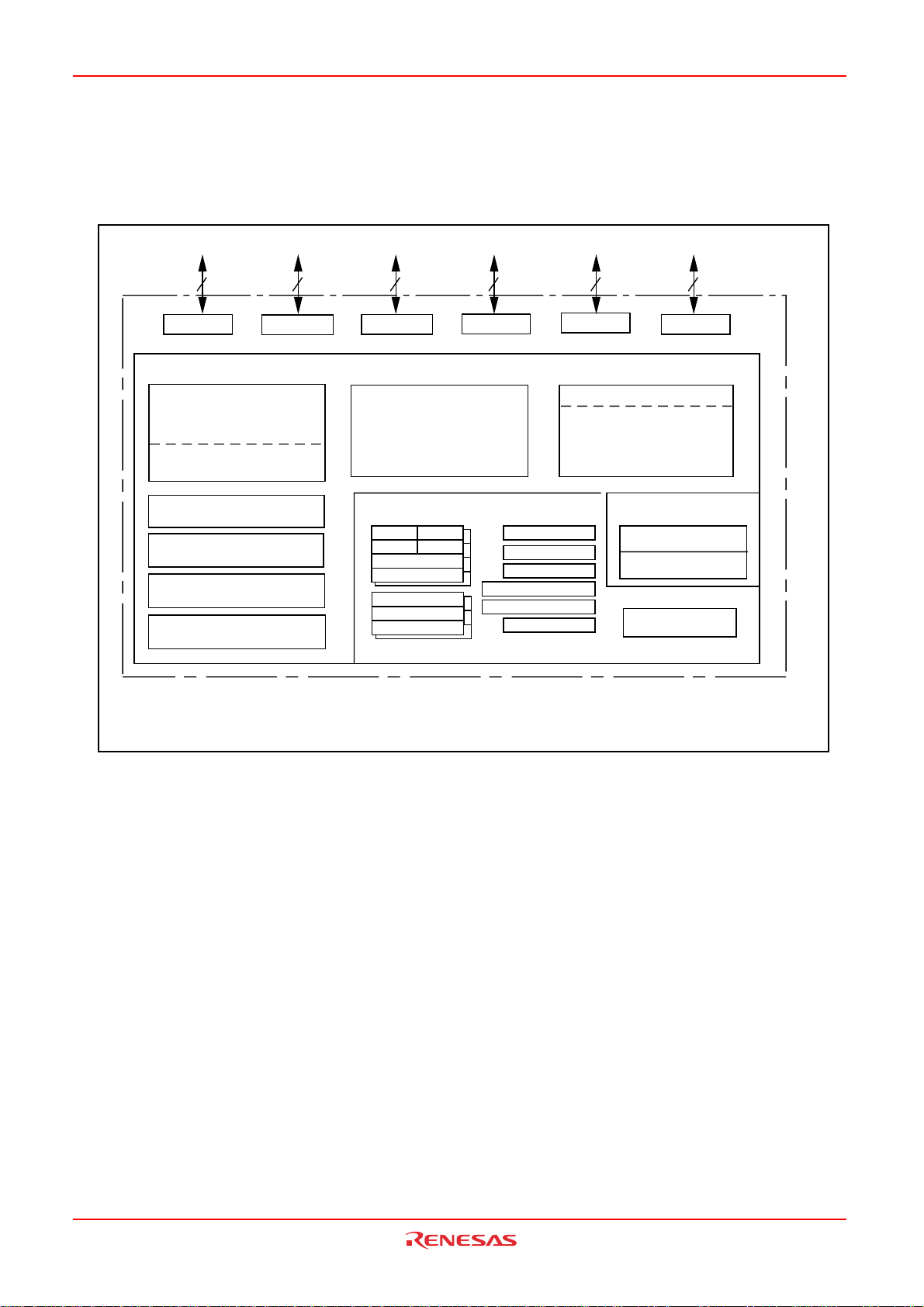
1.3 Block Diagram
Figure 1.1 and 1.2 show block diagrams of the M16C/26A Group (M16C/26A, M16C/26B, M16C/26T) 48-
pin package and 42-pin package.
3
Port P1
Peripheral functions
Timer (16-bit)
Output (timer A): 5channels
Input (timer B): 3 channels
Three-phase motor
control circuit
10-bit A/D converter
12 channels
Watchdog timer
(15 bits)
DMAC
(2 channels)
CRC calculation circuit
(CCITT, CRC-16 )
Port P6
Port P10
(1)
ROM
(2)
RAM
Multiplier
8
8
8
Port P7
UART or
clock synchronous serial I/O
(8 bits X 3 channels)
M16C/60 series CPU core
R0LR0H
R1H R1L
R2
R3
A0
A1
FB
8
Port P8
4
Port P9
Clock generation circuit
XIN-XOUT
XCIN-XCOUT
On-Chip Oscillator
PLL frequency synthesizer
Memory
SB
USP
ISP
INTB
PC
FLG
NOTES:
1: ROM size depends on the MCU type.
2: RAM size depends on the MCU type.
Figure 1.1 Block Diagram(48-pin Package)
page 4
923fo7002,51.beF00.2.veR
0020-2020B90JER
Page 22
)T62/C61M,B62/C61M,A62/C61M(puorGA62/C61M
1. Overview
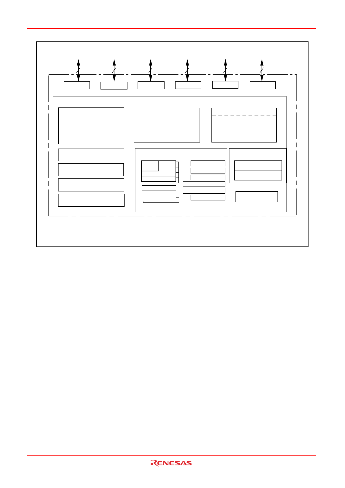
3
Port P1
Peripheral functions
Timer (16-bit)
Output (timer A): 5channels
Input (timer B): 3 channels
Three-phase motor
control circuit
10-bit A/D converter
10 channels
Watchdog timer
(15 bits)
DMAC
(2 channels)
CRC calculation circuit
(CCITT, CRC-16 )
Port P6
Port P10
(1)
ROM
(2)
RAM
Multiplier
8
4
8
Port P7
UART or
clock synchronous serial I/O
(8 bits X 2 channels)
M16C/60 series CPU core
R0LR0H
R1H R1L
R2
R3
A0
A1
FB
8
Port P8
2
Port P9
Clock generation circuit
XIN-XOUT
XCIN-XCOUT
On-Chip Oscillator
PLL frequency synthesizer
Memory
SB
USP
ISP
INTB
PC
FLG
NOTES:
1: ROM size depends on the MCU type.
2: RAM size depends on the MCU type.
Figure 1.2 Block Diagram( 42-pin Package)
page 5
923fo7002,51.beF00.2.veR
0020-2020B90JER
Page 23
)T62/C61M,B62/C61M,A62/C61M(puorGA62/C61M
1. Overview
1.4 Product List
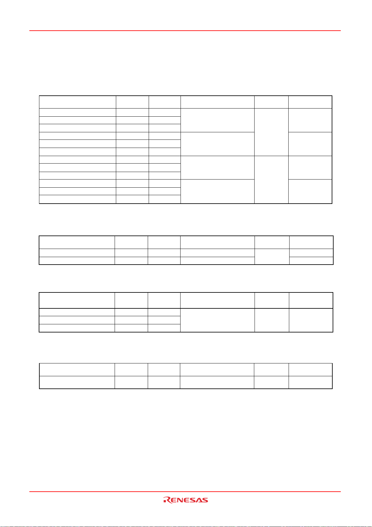
Tables 1.3 to 1.6 lists product information, Figure 1.3 shows a product numbering system, Table 1.7 lists
the product code, and Figure 1.4 shows the marking.
Table 1.3 M16C/26A Current as of Feb., 2007
rebmuNepyT
PGA3F06203M)N(K4+K42K1
PGA6F06203M)N(K4+K84K2
PGA8F06203M)N(K4+K46K2
PFA3F36203M)N(K4+K42K1
PFA6F36203M)N(K4+K84K2
PFA8F36203M)N(K4+K46K2
PGXXX-A3M06203M)N(K42K1
PGXXX-A6M06203M)N(K84K2
PGXXX-A8M06203M)N(K46K2
PFXXX-A3M36203M)N(K42K1
PFXXX-A6M36203M)N(K84K2
PFXXX-A8M36203M)N(K46K2
weN:)N(
MOR
yticapaC
MAR
yticapaC
epyTegakcaPskrameRedoCtcudorP
)A-Q6P84(A-BK8400PQLP
hsalF
yromem
)R2P24(B-AG2400PSRP9U,5U
)A-Q6P84(A-BK8400PQLP
MORksaM
)R2P24(B-AG2400PSRP5U
5U,3U
9U,7U,5U,3U
Table 1.4 M16C/26B Current as of Feb., 2007
rebmuNepyT
PGB8F06203M)N(K4+K46K2)A-Q6P84(A-BK8400PQLP
PFB8F36203M)N(K4+K46K2)R2P24(B-AG2400PSRP9U
weN:)N(
MOR
yticapaC
MAR
yticapaC
epyTegakcaPskrameRedoCtcudorP
hsalF
yromem
7U
Table 1.5 M16C/26T T-ver. Current as of Feb., 2007
rebmuNepyT
PGT3F06203MK4+K42K1
PGT6F06203MK4+K84K2
PGT8F06203MK4+K46K2
:ETON
MOR
yticapaC
.ylnonoisrevyromemhsalfnielbaliavA.1
MAR
yticapaC
epyTegakcaPskrameRedoCtcudorP
)A-Q6P84(A-BK8400PQLP
hsalF
yromem
7U,3U
Table 1.6 M16C/26T V-ver. Current as of Feb., 2007
rebmuNepyT
PGV8F06203MK4+K46K2)A-Q6P84(A-BK8400PQLP
:ETON
MOR
yticapaC
.ylnonoisrevyromemhsalfnielbaliavA.1
MAR
yticapaC
egakcaPskrameRedoCtcudorP
hsalF
yromem
7U,3U
page 6
923fo7002,51.beF00.2.veR
0020-2020B90JER
Page 24
Type No. M 3 0 2 6 0 M 8 A - XXX G P - U3
)T62/C61M,B62/C61M,A62/C61M(puorGA62/C61M
Product code:
See Tables 1.7 to 1.10
Package type:
GP: PLQP0048KB-A (48P6Q) (M16C/26A, M16C/26B, M16C/26T)
FP: PRSP0042GA-B (42P2R) (M16C/26A, M16C/26B)
ROM number:
ROM number is omitted in flash memory version
Version:
A : M16C/26A
B : M16C/26B
T : M16C/26T T-ver.
V : M16C/26T V-ver.
1. Overview
Figure 1.3 Product Numbering System
ROM / RAM capacity:
3: (24K+4K) bytes
6: (48K+4K) bytes
8: (64K+4K) bytes
NOTE:
1. Only flash memory version exists in "+4K bytes"
Memory type:
M: Mask ROM version
F: Flash memory version
Pin count (The value itself has no specific meaning)
M16C/26A Group
M16C Family
(1)
/ 1K bytes
(1)
/ 2K bytes
(1)
/ 2K bytes
page 7
923fo7002,51.beF00.2.veR
0020-2020B90JER
Page 25
)T62/C61M,B62/C61M,A62/C61M(puorGA62/C61M
Table 1.7 Product Code (Flash Memory Version) - M16C/26A, M16C/26B
MORlanretnI
tcudorP
edoC
3U
5U Cº58ot027U
9U Cº58ot02-Cº58ot02-
egakcaP
eerfdaeL
dnamargorP
esarE
ecnarudnE
001
000,1000,01
)3ot0skcolB:ecapSmargorP(
erutarepmeT
egnaR
Cº06ot0
dnamargorP
esarE
ecnarudnE
001Cº06ot0
MORlanretnI
)BdnaAskcolB:ecapSataD(
erutarepmeT
egnaR
Cº58ot04-Cº58ot04-
Table 1.8 Product Code (Mask ROM Version - M16C/26A)
1. Overview
tneibmAgnitarepO
erutarepmeT
Cº58ot04-
tcudorP
edoC
3U
egakcaP
Cº04-otCº58
tneibmAgnitarepO
erutarepmeT
eerfdaeL
5UCº02-otCº58
NOTE:
1. The lead contained products, D3, D5, D7, and D9 are put together with U3, U5, U7, and U9 respectively.
Lead-free products can be mounted by both conventional Sn-Pb paste and Lead-free paste (Sn-Ag-Cu
plating).
Table 1.9 Product Code (Flash Memory Version) - M16C/26T T-ver.
MORlanretnI
tcudorP
edoC
3U
7U000,1000,01
egakcaP
eerfdaeL
gnimmargorP
erusaredna
ecnarudne
001
)3ot0skcolB:ecapSmargorP(
erutarepmeT
egnar
Cº06otCº0
gnimmargorP
erusaredna
ecnarudne
001
MORlanretnI
)BdnaAskcolB:ecapSataD(
erutarepmeT
egnar
Cº58otCº04-Cº58otCº04-
tneibmAgnitarepO
erutaremeT
Table 1.10 Product Code (Flash Memory Version) - M16C/26T V-ver.
MORlanretnI
tcudorP
edoC
3U
7U000,1000,01
egakcaP
eerfdaeL
gnimmargorP
erusaredna
ecnarudne
001
)3ot0skcolB:ecapSmargorP(
erutarepmeT
egnar
Cº06otCº0
gnimmargorP
erusaredna
ecnarudne
001
MORlanretnI
)BdnaAskcolB:ecapSataD(
erutarepmeT
egnar
Cº521otCº04-Cº521otCº04-
tneibmAgnitarepO
erutaremeT
page 8
0020-2020B90JER
923fo7002,51.beF00.2.veR
Page 26
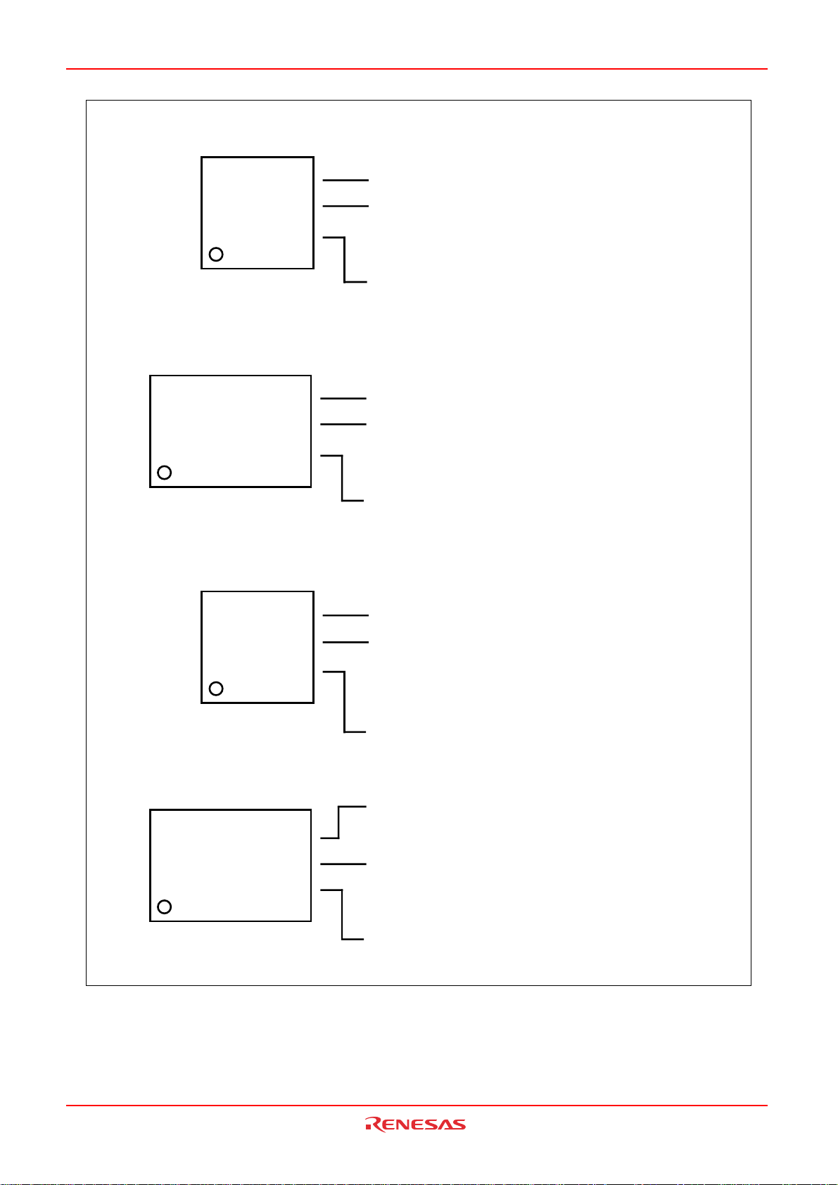
)T62/C61M,B62/C61M,A62/C61M(puorGA62/C61M
(1) Flash memory version, PLQP0048KB-A (48P6Q), M16C/26A, M16C/26B
1. Overview
0260F8A
A U3
XXXXX
(2) Flash memory version, PRSP0042GA-B (42P2R), M16C/26A, M16C/26B
M30263F8AFP
A U3
XXXXXXX
(3) MASK ROM version, PLQP0048KB-A (48P6Q), M16C/26A
Product Name : indicates M30260F8AGP
Chip Version and Product Code:
A : Indicates chip version
The first edition is shown to be blank and continues
with A and B.
U3 : Indicates Product code (see Table 1.7 Product Code)
Date Code (5 digits) fi indicates manufacturing management code
Product Name : indicates M30263F8AFP
Chip Version and Product Code:
A : Indicates chip version
The first edition is shown to be blank and continues
with A and B.
U3 : Indicates Product code (see Table 1.7 Product Code)
Date Code (7 digits) fi indicates manufacturing management code
0260M8A
001A U3
XXXXX
(4) MASK ROM version, PRSP0042GA-B (42P2R), M16C/26A
M30263M8A-001FP
A U3
Product Name : indicates M30260M8AGP
ROM number, Chip Version and Product Code:
001: Indicates ROM Number
A : Indicates chip version
U3 : Indicates Product code (see Table 1.8 Product Code)
Date Code (5 digits) fi indicates manufacturing management code
Product Name and ROM number
M30263M8A and FP are indicated of Produnct name
001 is indicated of ROM number
Chip Version and Product Code:
A : Indicates chip version
XXXXXXX
U3 : Indicates Product code (see Table 1.8 Product Code)
Date Code (7 digits) fi indicates manufacturing management code
Figure 1.4 Marking Diagram (M16C/26A , M16C/26B)
The first edition is shown to be blank and continues
with A and B.
The first edition is shown to be blank and continues
with A and B.
page 9
923fo7002,51.beF00.2.veR
0020-2020B90JER
Page 27
)T62/C61M,B62/C61M,A62/C61M(puorGA62/C61M
(1) Flash memory version, PLQP0048KB-A (48P6Q), M16C/26T T-ver.
1. Overview
0260F8T
A U3
Product Name : indicates M30260F8TGP
Chip Version and Product Code:
XXXXX
Date Code (5 digits) fi indicates manufacturing management code
(2) Flash memory version, PLQP0048KB-A (48P6Q), M16C/26T V-ver.
0260F8V
A U3
Product Name : indicates M30260F8VGP
Chip Version and Product Code:
XXXXX
Date Code (5 digits) fi indicates manufacturing management code
Figure 1.5 Marking Diagram (M16C/26T)
A : Indicates chip version
The first edition is shown to be blank and continues
with A and B.
U3 : Indicates product code (see Table 1.9 Product Code)
A : Indicates chip version
The first edition is shown to be blank and continues
with A and B.
U3 : Indicates product code (see Table 1.10 Product Code)
page 10
923fo7002,51.beF00.2.veR
0020-2020B90JER
Page 28
)T62/C61M,B62/C61M,A62/C61M(puorGA62/C61M
p
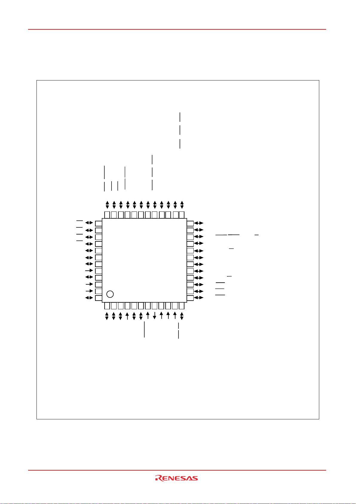
1.5 Pin Assignments
Figures 1.6 and 1.7 show the Pin Assignments (top view).
1
/CLKS
0
/IDV
TRG
/AD
3
/INT
5
P1
/IDW
4
/INT
6
P1
/IDU
5
/INT
7
P1
0
/RTS
0
/CTS
0
P6
0
/CLK
1
P6
0
/RxD
2
P6
0
/TxD
3
P6
/CTS
1
/RTS
1
/CTS
4
P6
1
/CLK
5
P6
1
/RxD
6
P6
1
/TxD
7
P6
1
/CLKS
0
/CTS
1
/RTS
1
/CTS
2
/SDA
0OUT
/TA
2
/TxD
0
P7
1. Overview
P107/AN7/KI
P106/AN6/KI
P105/AN5/KI
P104/AN4/KI
P103/AN
P102/AN
P101/AN
AV
P100/AN
V
REF
AV
P93/AN
35
2
31
/AN
IN
/TB1
1
P9
34
3
OUT
/CLK
30
/AN
IN
/TB0
0
33
4
SS
CNV
32
5
CIN
/X
7
P8
31
6
COUT
/X
6
P8
30
7
RESET
36
3
37
2
38
1
39
0
40
41
3
2
42
1
43
ss
44
0
45
46
cc
47
24
48
1
32
/AN
IN
/TB2
2
P9
P9
29
8
OUT
X
SS
V
27
28
9
25
26
24
P71/RxD2/TA0IN/SCL2/CLK1
P72/CLK2/TA1
23
22
P73/CTS2/RTS2/TA1IN/V/TxD
21
P74/TA2
20
19
18
17
16
15
14
13
11
10
12
IN
CC
X
V
/NMI/SD
5
5
/TA2IN/W
P7
P76/TA3
P77/TA3
P80/TA4
1
/TA4IN/U
P8
2
/INT
P8
P83/INT
P84/INT2/ZP
OUT
OUT
IN
OUT
0
1
/W
/U
OUT
/V/RxD
1
1
P8
NOTE:
1. Set PACR2 to PACR0 bit in the PACR register
2
to "100
" before you input and output it after
resetting to each pin. When the PACR register
isn't set up, the input and output function of
some of the
ins are disabled.
Figure 1.6 Pin Assignment for 48-Pin Package (Top View)
page 11
0020-2020B90JER
923fo7002,51.beF00.2.veR
Package: PLQP0048KB-A (48P6Q)
Page 29
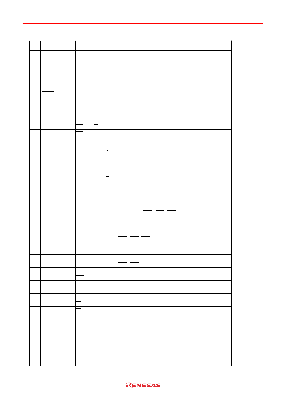
)T62/C61M,B62/C61M,A62/C61M(puorGA62/C61M
Table 1.11 Pin Characteristics for 48-Pin Package
niP
.oN
19P
29P
39P
4ssVNC
5X
6X
7TESER
8X
9ssV
01X
11ccV
218P
318P
418P
518P
618P
718P
817P
917P
027P
127P
227P
327P
427P
527P
626P
726P
826P
926P
036P
136P
236P
336P
431P
531P
631P
7301P
8301P
9301P
0401P
1401P
2401P
3401P
44ssVA
5401P
64V
74ccVA
849P
lortnoC
niP
NIC
TUOC
TUO
NI
FER
troP
2
1
0
8P
7
8P
6
5
4
3
2
1
0
7
6
5
4
3
2
1
0
7
6
5
4
3
2
1
0
7
6
5
7
6
5
4
3
2
1
0
3
niP
IMNDS
TNI
2
TNI
1
TNI
0
TNI
5
TNI
4
TNI
3
IK
3
IK
2
IK
1
IK
0
tpurretnI
BT
BT
BT
niPremiTniPTRAUniPgolanA
NI2
NI1
NI0
KLC
TUO
PZ
AT
NI4
U/
AT
TUO4
U/
AT
NI3
AT
TUO3
AT
NI2
W/
AT
TUO2
W/
AT
NI1
AT
AT
AT
V/STC
TUO1
NI0
TUO0
V/KLC2R/XD
RXD
TXD
TXD
RXD
TXD
RXD
2
STR/
2T/XD1
1
2
LCS/
2
2
ADS/
2
1
1
KLC
1
STR
1
STC/
1
0
0
KLC
0
STR
0
STC/
0
UDI
WDI
VDIDA
1. Overview
3NA
2
3NA
1
3NA
0
KLC/
1
STR/
1
STC/
1
STC/
0
SKLC/
1
STC/
0
SKLC/
1
GRT
NA
7
NA
6
NA
5
NA
4
NA
3
NA
2
NA
1
NA
0
2NA
4
page 12
923fo7002,51.beF00.2.veR
0020-2020B90JER
Page 30
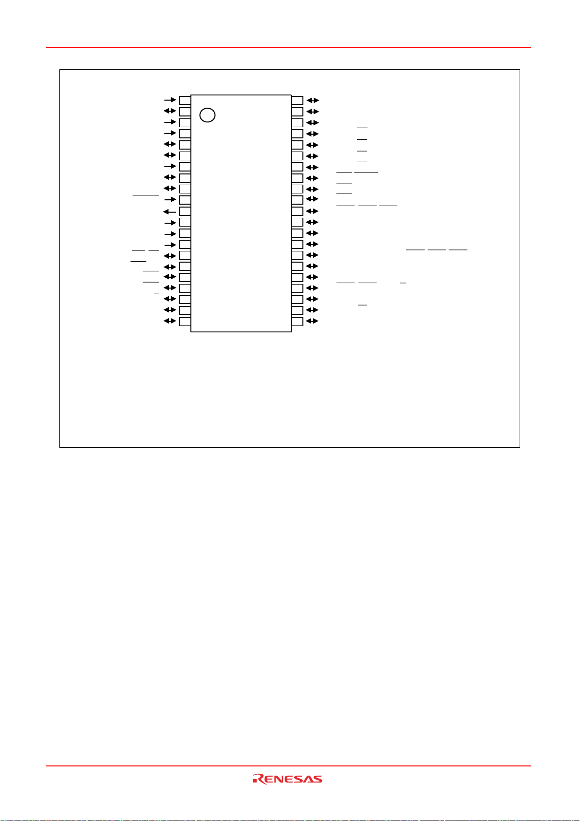
)T62/C61M,B62/C61M,A62/C61M(puorGA62/C61M
p
1. Overview
AVSS
P100/AN0
VREF
AVCC
P91/TB1IN/AN31
P90/TB0IN/AN30/CLKout
CNVSS
P87/XCIN
P86/XCOUT
RESET
XOUT
VSS
XIN
VCC
P85/NMI/SD
P84/INT2/ZP
P83/INT1
P82/INT0
P81/TA4IN/U
P8
0/TA4OUT/U
P7
7/TA3IN
1
2
3
4
5
6
7
8
9
10
11
12
13
14
15
16
17
18
19
20
21
42
41
40
39
38
37
36
35
34
33
32
31
30
29
28
27
26
25
24
23
22
P101/AN1
P102/AN2
P103/AN3
P104/AN4/KI0
P105/AN5/KI1
P106/AN6/KI2
P107/AN7/KI3
P15/INT3/ADTRG/IDV
P16/INT4/IDW
P17/INT5/IDU
P64/CTS1/RTS1/CTS0/CLKS1
P65/CLK1
P66/RxD1
P67/TxD1
P70/TxD2/SDA2/TA0OUT/CTS1/RTS1/CTS0/CLKS1
P71/RxD2/SCL2/TA0IN/CLK1
P72/CLK2/TA1OUT/V/RxD1
P73/CTS2/RTS2/TA1IN/V/TxD1
P7
4/TA2OUT/W
P75/TA2IN/W
P76/TA3OUT
NOTE:
1. Set PACR2 to PACR0 bit in the PACR register
to "001
2
" before you input and output it after
resetting to each pin. When the PACR register
isn't set up, the input and output function of
some of the
ins are disabled.
Figure 1.7 Pin Assignment for 42-Pin Package (Top View)
Package: PRSP0042GA-B (42P2R)
page 13
923fo7002,51.beF00.2.veR
0020-2020B90JER
Page 31

)T62/C61M,B62/C61M,A62/C61M(puorGA62/C61M
Table 1.12 Pin Characteristics for 42-Pin Package
niP
.oN
1ssVA
201P
3V
4VA
59P
69P
7ssVNC
8X
9X
01TESER
11X
21ssV
31X
41V
518P
618P
718P
818P
918P
028P
127P
227P
327P
427P
527P
627P
727P
827P
926P
036P
136P
236P
331P
431P
531P
6301P
7301P
8301P
9301P
0401P
1401P
2401P
lortnoC
niP
FER
CC
NIC
TUOC
TUO
NI
CC
troP
0
1
0
8P
7
8P
6
5
4
3
2
1
0
7
6
5
4
3
2
1
0
7
6
5
4
7
6
5
7
6
5
4
3
2
1
niP
IMNDS
TNI
2
TNI
1
TNI
0
TNI
5
TNI
4
TNI
3
IK
3
IK
2
IK
1
IK
0
tpurretnI
BT
BT
niPremiTniPTRAUniPgolanA
NI1
NI0
KLC
TUO
PZ
AT
NI4
U/
AT
TUO4
U/
AT
NI3
AT
TUO3
AT
NI2
W/
AT
TUO2
W/
AT
NI1
AT
AT
AT
TUO1
NI0
TUO0
V/STC
V/KLC
RXD
TXD
TXD
RXD
2
2R/XD1
2
2
1
1
KLC
1
STR
1
STR/
2T/XD1
LCS/
2
ADS/
2
STC/
1
UDI
WDI
VDIDA
1. Overview
NA
0
3NA
1
3NA
0
KLC/
1
STR/
1
STC/
1
STC/
0
SKLC/
1
STC/
0
SKLC/
1
GRT
NA
7
NA
6
NA
5
NA
4
NA
3
NA
2
NA
1
page 14
923fo7002,51.beF00.2.veR
0020-2020B90JER
Page 32

)T62/C61M,B62/C61M,A62/C61M(puorGA62/C61M
1.6 Pin Description
Table 1.13 Pin Description (48-Pin and 42-Pin Packages)
Classification Pin Name I/O Type Description
Power Supply
Analog Power
Supply
Reset Input
CNVSS
Main Clock
VCC, VSS
AVCC
AVSS
____________
RESET
CNVSS
XIN
Input
Main Clock
XOUT
Output
Sub Clock Input
Sub Clock Output
Clock Output
______
INT Interrupt
Input
_______
NMI Interrupt
XCIN
XCOUT
CLKOUT
________ ________
INT0 to INT5
_______
NMI
Input
Key Input Interrupt
Timer A
_____ _____
KI0 to KI3
TA0OUT to
I/O
TA4OUT
TA0IN to
TA4IN
ZP
Timer B
Three-Phase
Motor Control
Timer Output
Serial I/O
TB0
IN to
TB1IN
___ ___
U, U, V, V,
___
W, W
IDU, IDW,
_____
IDV, SD
_________ _________
CTS1 to CTS2
_________ _________
RTS1 to RTS2
CLK1 to CLK2
I/O
I/O
RxD1 to RxD2
TxD1 to TxD2
CLKS1
Reference
V
REF
Voltage Input
A/D Converter
I/O Ports
AN0 to AN7
AN30 to AN3
___________
ADTRG
P15 to P17
P64 to P67
1
I/O
I/O
P70 to P77
P80 to P87
P100 to P10
7
P90 to P91
I : Input O : Output I/O : Input and output
Apply 0V to the Vss pin. Apply following voltage to the Vcc pin.
I
2.7 to 5.5 V (M16C/26A, M16C/26B), 3.0 to 5.5 V (M16C/26T T-ver.), 4.2
to 5.5 V (M16C/26T V-ver.)
Supplies power to the A/D converter. Connect the AVCC pin to VCC and
I
the AVSS pin to VSS
The MCU is in a reset state when "L" is applied to the RESET pin
I
Connect the CNVSS pin to VSS
I
I/O pins for the main clock oscillation circuit. Connect a ceramic resonator
I
or crystal oscillator between X
it to XIN and leave XOUT open. If XIN is not used (for external oscillator or
O
IN and XOUT. To apply external clock, apply
external clock), connect XIN pin to VCC and leave XOUT open
I/O pins for the sub clock oscillation circuit. Connect a crystal oscillator
I
between XCIN and XCOUT
O
Outputs the clock having the same frequency as f1, f8, f32, or fC
O
Input pins for the INT interrupt. INT2 can be used for Timer A Z-phase
I
function
_______ _______
NMI
I
interrupt input pin.
______ ________
NMI
cannot be used as I/O port while the three-phase
motor control is enabled. Apply a stable "H" to NMI after setting it's direction
register to "0" when the three-phase motor control is enabled
Input pins for the key input interrupt
I
I/O pins for the timer A0 to A4
Input pins for the timer A0 to A4
I
Input pin for Z-phase
I
Timer B0 to B1 input pins
I
Output pins for the three-phase motor control timer
O
I/O pins for the three-phase motor control timer
Input pins to control data transmission
I
Output pins to control data reception
O
Inputs and outputs the transfer clock
Inputs serial data
I
Outputs serial data
O
Output pin for transfer clock
O
Applies reference voltage to the A/D converter
I
Analog input pins for the A/D converter
I
Input pin for an external A/D trigger
I
I/O ports for CMOS. Each port can be programmed for input or output
under the control of the direction register. An input port can be set, by
program, for a pull-up resistor available or for no pull-up resister available
in 3-bit units
CMOS I/O ports which have a direction register determines an individual
pin used as an input port or an output port. A pull-up resistor is selectable
for every 4 input ports
1. Overview
___________
_______
page 15
923fo7002,51.beF00.2.veR
0020-2020B90JER
Page 33

)T62/C61M,B62/C61M,A62/C61M(puorGA62/C61M
Table 1.13 Pin Description ( 48-pin packages only) (Continued)
Classification Pin Name I/O Type Description
Serial I/O
Timer B
A/D Converter
I/O Ports
_________
CTS0
_________
RTS0
CLK0
RxD0
TxD0
TB2IN
AN2
4
AN32
P60 to P63
P92 to P93
O
I/O
O
I/O
Inputs pin to control data transmission
I
Output pin to control data reception
Inputs and outputs the transfer clock
Inputs serial data
I
Outputs serial data
Timer B2 input pin
I
Analog input pins for the A/D converter
I
CMOS I/O ports which have a direction register determines an individual
pin used as an input port or an output port. A pull-up resistor is selectable
for every 4 input ports
I : Input O : Output I/O : Input and output
1. Overview
page 16
923fo7002,51.beF00.2.veR
0020-2020B90JER
Page 34

)T62/C61M,B62/C61M,A62/C61M(puorGA62/C61M
b15
b0
b7
b8
b
2. Central Processing Unit (CPU)
Figure 2.1 shows the CPU registers. The register bank is comprised of seven registers (R0, R1, R2, R3,
A0, A1 and FB) out of 13 registers. There are two sets of register bank.
2. CPU
b31
R2
R3
NOTE:
1. These registers comprise a register bank. There are two register banks.
b15
R0H(R0's high bits)
R1H(R1's high bits)
b19
b15
INTBH
The upper 4 bits of INTB are INTBH and
the lower 16 bits of INTB are INTBL.
b19
b15
b15
b8 b7 b0
R0L(R0's low bits)
R1L(R1's low bits)
R2
R3
A0
A1
FB
INTBL
PC
USP
ISP
SB
FLG
Data registers (1)
Address registers (1)
Frame base registers (1)
b0
Interrupt table register
b0
Program counter
b0
User stack pointer
Interrupt stack pointer
Static base register
b0
Flag register
Carry flag
Debug flag
Zero flag
Sign flag
Register bank select flag
Overflow flag
Interrupt enable flag
Stack pointer select flag
Reserved area
Processor interrupt priority level
Reserved area
Figure 2.1. CPU Register
2.1 Data Registers (R0, R1, R2 and R3)
The R0 register consists of 16 bits, and is used mainly for transfers and arithmetic/logic operations. R1 to
R3 are the same as R0.
The R0 register can be separated between high (R0H) and low (R0L) for use as two 8-bit data registers.
R1H and R1L are the same as R0H and R0L. Conversely, R2 and R0 can be combined for use as a 32-bit
data register (R2R0). R3R1 is the same as R2R0.
2.2 Address Registers (A0 and A1)
The register A0 consists of 16 bits, and is used for address register indirect addressing and address register relative addressing. They also are used for transfers and arithmetic/logic operations. A1 is the same as
A0.
In some instructions, registers A1 and A0 can be combined for use as a 32-bit address register (A1A0).
page 17
0020-2020B90JER
923fo7002,51.beF00.2.veR
Page 35

)T62/C61M,B62/C61M,A62/C61M(puorGA62/C61M
2.3 Frame Base Register (FB)
FB is configured with 16 bits, and is used for FB relative addressing.
2.4 Interrupt Table Register (INTB)
INTB is configured with 20 bits, indicating the start address of an interrupt vector table.
2.5 Program Counter (PC)
PC is configured with 20 bits, indicating the address of an instruction to be executed.
2.6 User Stack Pointer (USP) and Interrupt Stack Pointer (ISP)
Stack pointer (SP) comes in two types: USP and ISP, each configured with 16 bits.
Your desired type of stack pointer (USP or ISP) can be selected by the U flag of FLG.
2.7 Static Base Register (SB)
SB is configured with 16 bits, and is used for SB relative addressing.
2.8 Flag Register (FLG)
FLG consists of 11 bits, indicating the CPU status.
2.8.1 Carry Flag (C Flag)
This flag retains a carry, borrow, or shift-out bit that has occurred in the arithmetic/logic unit.
2.8.2 Debug Flag (D Flag)
2. CPU
The D flag is used exclusively for debugging purpose. During normal use, it must be set to 0.
2.8.3 Zero Flag (Z Flag)
This flag is set to 1 when an arithmetic operation resulted in 0; otherwise, it is 0.
2.8.4 Sign Flag (S Flag)
This flag is set to 1 when an arithmetic operation resulted in a negative value; otherwise, it is 0.
2.8.5 Register Bank Select Flag (B Flag)
Register bank 0 is selected when this flag is 0 ; register bank 1 is selected when this flag is 1.
2.8.6 Overflow Flag (O Flag)
This flag is set to 1 when the operation resulted in an overflow; otherwise, it is 0.
2.8.7 Interrupt Enable Flag (I Flag)
This flag enables a maskable interrupt.
Maskable interrupts are disabled when the I flag is 0, and are enabled when the I flag is 1.
The I flag is cleared to 0 when the interrupt request is accepted.
2.8.8 Stack Pointer Select Flag (U Flag)
ISP is selected when the U flag is 0; USP is selected when the U flag is 1.
The U flag is cleared to 0 when a hardware interrupt request is accepted or an INT instruction for software
interrupt Nos. 0 to 31 is executed.
2.8.9 Processor Interrupt Priority Level (IPL)
IPL is configured with three bits, for specification of up to eight processor interrupt priority levels from level
0 to level 7.
If a requested interrupt has priority greater than IPL, the interrupt is enabled.
2.8.10 Reserved Area
When write to this bit, write 0. When read, its content is undefined.
page 18
0020-2020B90JER
923fo7002,51.beF00.2.veR
Page 36

)T62/C61M,B62/C61M,A62/C61M(puorGA62/C61M
3. Memory
Figure 3.1 is a memory map of the M16C/26A Group (M16C/26A, M16C/26B, M16C/26T). The M16C/26A
Group provides 1-Mbyte address space addresses 0000016 to FFFFF16.
The internal ROM is allocated lower address, beginning with address FFFFF16. For example, a 64-Kbyte
internal ROM area is allocated in addresses F000016 to FFFFF16. The flash memory version has two sets
of 2-Kbyte internal ROM area, block A and block B, for data space. These blocks are allocated addresses
F00016 to FFFF16.
The fixed interrupt vectors are allocated addresses FFFDC16 to FFFFF16 and they store the start address
of each interrupt routine.
The internal RAM is allocated higher addresses, beginning with address 0040016. For example, a 1-Kbyte
internal RAM area is allocated in addresses 0040016 to 007FF16. The internal RAM is used for temporarily
storing data. The area is also used as stacks when subroutines are called or interrupt requests are acknowledged.
The SFR is allocated addresses 0000016 to 003FF16. The peripheral function control registers are allocated here. All blank spaces within SFR location are reserved and cannot be accessed by users.
The special page vectors are allocated addresses FFE0016 to FFFDB16. They are used for the JMPS
instruction and JSRS instruction. Refer to the Renesas publication M16C/60 and M16C/20 Series Soft-
ware Manual for details.
3. Memory
24K bytes
48K bytes
64K bytes
Internal ROM
Address YYYYY
FA00016
F4000
F0000
Internal RAM
Size
Address XXXXX16
1K bytes 007FF16
2K bytes
NOTE:
1. Block A (2 Kbytes) and block B (2 Kbytes).
2. Do not write to the internal ROM in Mask ROM version.
00BFF16
Figure 3.1 Memory Map
0000016
SFR
0040016
Internal RAM
XXXXX16
0F00016
16Size
0FFFF16
16
16
YYYYY16
FFFFF16
Reserved
Internal ROM
(Data space)
Reserved
Internal ROM
(Program space)
(1)
(2)
FFE0016
FFFDC16
FFFFF16
Special page
vector table
Undefined instruction
Overflow
BRK instruction
Address match
Single step
Watchdog timer
DBC
NMI
Reset
page 19
923fo7002,51.beF00.2.veR
0020-2020B90JER
Page 37

)T62/C61M,B62/C61M,A62/C61M(puorGA62/C61M
4. Special Function Registers (SFRs)
Table 4.1 SFR Information(1)
Address
0000
16
0001
16
0002
16
0003
16
0004
16
Processor mode register 0 PM0 00
0005
16
Processor mode register 1 PM1 00001000
0006
16
System clock control register 0 CM0 01001000
0007
16
System clock control register 1 CM1 00100000
0008
16
0009
16
Address match interrupt enable register AIER XXXXXX00
000A
16
Protect register PRCR XX000000
000B
16
000C
16
Oscillation stop detection register
000D
16
000E
16
Watchdog timer start register WDTS XX
000F
16
Watchdog timer control register WDC 00XXXXXX
0010
16
Address match interrupt register 0 RMAD0 00
0011
16
0012
16
0013
16
0014
16
Address match interrupt register 1 RMAD1 00
0015
16
0016
16
0017
16
0018
16
0019
16
Voltage detection register 1
001A
16
Voltage detection register 2
001B
16
001C
16
PLL control register 0 PLC0 0001X010
001D
16
001E
16
Processor mode register 2 PM2 XXX00000
001F
16
Low voltage detection interrupt register
DMA0 source pointer SAR0 XX
0020
16
0021
16
0022
16
0023
16
DMA0 destination pointer DAR0 XX
0024
16
0025
16
0026
16
0027
16
DMA0 transfer counter TCR0 XX
0028
16
0029
16
002A
16
002B
16
DMA0 control register DM0CON 00000X00
002C
16
002D
16
002E
16
002F
16
DMA1 source pointer SAR1 XX
0030
16
0031
16
0032
16
0033
16
DMA1 destination pointer DAR1 XX
0034
16
0035
16
0036
16
0037
16
DMA1 transfer counter TCR1 XX
0038
16
0039
16
003A
16
003B
16
DMA1 control register DM1CON 00000X00
003C
16
003D
16
003E
16
003F
16
NOTES:
1. The blank spaces are reserved. No access is allowed.
2. Bits CM27, CM21, and CM20 do not change at oscillation stop detection reset.
3. The VCR1 and VCR2 registers do not change at software reset, watchdog timer reset, and oscillation stop detection reset.
4. Registers VCR1, VCR2, and D4INT cannot be used in M16C/26T.
5. M16C/26A, M16C/26B
X : Undefined
(1)
Register Symbol After reset
16
01101000
(2)
(3, 4)
(3, 4)
(4)
CM2 0X000000
16
16
00
16
X0
16
16
00
16
X0
16
VCR1 00001000
VCR2 00
D4INT 00
XX
XX
XX
XX
XX
XX
XX
XX
XX
XX
16
16
16
16
16
16
16
16
16
16
16
16
16
16
16
16
16
16
2
(5)
2
2(M16C/26T)
2
2
2
2
2
2
2
2
2
2
4. SFRs
page 20
923fo7002,51.beF00.2.veR
0020-2020B90JER
Page 38

)T62/C61M,B62/C61M,A62/C61M(puorGA62/C61M
4. SFRs
Table 4.2 SFR Information(2)
(1)
Address Register Symbol After reset
004016
004116
004216
004316
004416
INT3 interrupt control register INT3IC XX00X000
004516
004616
004716
004816
INT5 interrupt control register INT5IC XX00X000
004916
INT4 interrupt control register INT4IC XX00X000
004A16
UART2 Bus collision detection interrupt control register BCNIC XXXXX000
004B16
DMA0 interrupt control register DM0IC XXXXX000
004C16
DMA1 interrupt control register DM1IC XXXXX000
004D16
Key input interrupt control register KUPIC XXXXX000
004E16
A/D conversion interrupt control register ADIC XXXXX000
004F16
UART2 transmit interrupt control register S2TIC XXXXX000
005016
UART2 receive interrupt control register S2RIC XXXXX000
005116
UART0 transmit interrupt control register S0TIC XXXXX000
005216
UART0 receive interrupt control register S0RIC XXXXX000
005316
UART1 transmit interrupt control register S1TIC XXXXX000
005416
UART1 receive interrupt control register S1RIC XXXXX000
005516
TimerA0 interrupt control register TA0IC XXXXX000
005616
TimerA1 interrupt control register TA1IC XXXXX000
005716
TimerA2 interrupt control register TA2IC XXXXX000
005816
TimerA3 interrupt control register TA3IC XXXXX000
005916
TimerA4 interrupt control register TA4IC XXXXX000
005A16
TimerB0 interrupt control register TB0IC XXXXX000
005B16
TimerB1 interrupt control register TB1IC XXXXX000
005C16
TimerB2 interrupt control register TB2IC XXXXX000
005D16
INT0 interrupt control register INT0IC XX00X000
005E16
INT1 interrupt control register INT1IC XX00X000
005F16
INT2 interrupt control register INT2IC XX00X000
006016
006116
006216
006316
006416
006516
006616
006716
006816
006916
006A16
006B16
006C16
006D16
006E16
006F16
007016
007116
007216
007316
007416
007516
007616
007716
007816
007916
007A16
007B16
007C16
007D16
007E16
007F16
NOTE:
1. Blank spaces are reserved. No access is allowed.
X: Undefined
2
2
2
2
2
2
2
2
2
2
2
2
2
2
2
2
2
2
2
2
2
2
2
2
2
page 21
923fo7002,51.beF00.2.veR
0020-2020B90JER
Page 39

)T62/C61M,B62/C61M,A62/C61M(puorGA62/C61M
4. SFRs
Table 4.3 SFR Information(3)
Address
008016
008116
008216
008316
008416
008516
008616
~
~
01B016
01B116
01B216
01B316
01B416
01B516
01B616
01B716
01B816
01B916
01BA16
01BB16
01BC16
01BD16
01BE16
01BF16
Flash memory control register 4 (2) FMR4 010000002
Flash memory control register 1 (2) FMR1 000XXX0X2
Flash memory control register 0 (2) FMR0 0116
(1)
Register Symbol After reset
~
~
~
~
025016
025116
025216
025316
025416
025516
025616
025716
025816
025916
025A16
025B16
025C16
025D16
025E16
025F16
~
~
033016
033116
033216
033316
033416
033516
033616
033716
033816
033916
033A16
033B16
033C16
033D16
033E16
033F16
NOTES:
1. Blank spaces are reserved. No access is allowed.
2. This register is included in the flash memory version.
X: Undefined
Three phase protect control register TPRC 0016
On-chip oscillator control register ROCR X00001012
Pin assignment control register PACR 0016
Peripheral clock select register PCLKR 000000112
NMI digital debounce register NDDR FF16
Port17 digital debounce register P17DDR FF16
~
~
~
~
page 22
923fo7002,51.beF00.2.veR
0020-2020B90JER
Page 40

)T62/C61M,B62/C61M,A62/C61M(puorGA62/C61M
4. SFRs
Table 4.4 SFR Information(4)
(1)
Address Register Symbol After reset
0340
16
0341
16
0342
16
Timer A1-1 register TA11 XX
0343
16
0344
16
Timer A2-1 register TA21 XX
0345
16
0346
16
Timer A4-1 register TA41 XX
0347
16
0348
16
Three phase PWM control register 0 INVC0 00
0349
16
Three phase PWM control register 1 INVC1 00
034A
16
Three phase output buffer register 0 IDB0 00111111
034B
16
Three phase output buffer register 1 IDB1 00111111
034C
16
Dead time timer DTT XX
034D
16
Timer B2 Interrupt occurrence frequency set counter ICTB2 XX
034E
16
Position-data-retain function control register PDRF XXXX0000
034F
16
0350
16
0351
16
0352
16
0353
16
0354
16
0355
16
0356
16
0357
16
0358
16
Port function control register PFCR 00111111
0359
16
035A
16
035B
16
035C
16
035D
16
035E
16
Interrupt request cause select register 2 IFSR2A XXXXXXX0
035F
16
Interrupt request cause select register IFSR 00
0360
16
0361
16
0362
16
0363
16
0364
16
0365
16
0366
16
0367
16
0368
16
0369
16
036A
16
036B
16
036C
16
036D
16
036E
16
036F
16
0370
16
0371
16
0372
16
0373
16
0374
16
UART2 special mode register 4 U2SMR4 00
0375
16
UART2 special mode register 3 U2SMR3 000X0X0X
0376
16
UART2 special mode register 2 U2SMR2 X0000000
0377
16
UART2 special mode register U2SMR X0000000
0378
16
UART2 transmit/receive mode register U2MR 00
0379
16
UART2 bit rate register U2BRG XX
037A
16
UART2 transmit buffer register U2TB XXXXXXXX
037B
16
037C
16
UART2 transmit/receive control register 0 U2C0 00001000
037D
16
UART2 transmit/receive control register 1 U2C1 00000010
037E
16
UART2 receive buffer register U2RB XXXXXXXX
037F
16
16
XX
16
16
XX
16
16
XX
16
16
16
16
16
16
16
16
16
XXXXXXXX
XXXXXXXX
NOTE:
1. Blank spaces are reserved. No access is allowed.
2. Write "1" to bit 0 after reset.
X : Undefined
2
2
2
2
(2)
2
2
2
2
2
2
2
2
2
2
page 23
923fo7002,51.beF00.2.veR
0020-2020B90JER
Page 41

)T62/C61M,B62/C61M,A62/C61M(puorGA62/C61M
4. SFRs
Table 4.5 SFR Information(5)
(1)
Address Register Symbol After reset
038016
Count start flag TABSR 00
038116
Clock prescaler reset flag CPSRF 0XXXXXXX
038216
One-shot start flag ONSF 00
038316
Trigger select register TRGSR 00
038416
Up-dowm flag UDF 00
038516
038616
Timer A0 register TA0 XX
038716
038816
Timer A1 register TA1 XX
038916
038A16
Timer A2 register TA2 XX
038B16
038C16
Timer A3 register TA3 XX
038D16
038E16
Timer A4 register TA4 XX
038F16
039016
Timer B0 register TB0 XX
039116
039216
Timer B1 register TB1 XX
039316
039416
Timer B2 register TB2 XX
039516
039616
Timer A0 mode register TA0MR 00
039716
Timer A1 mode register TA1MR 00
039816
Timer A2 mode register TA2MR 00
039916
Timer A3 mode register TA3MR 00
039A16
Timer A4 mode register TA4MR 00
039B16
Timer B0 mode register TB0MR 00XX0000
039C16
Timer B1 mode register TB1MR 00XX0000
039D16
Timer B2 mode register TB2MR 00XX0000
039E16
Timer B2 special mode register TB2SC X0000000
039F16
03A016
UART0 transmit/receive mode register U0MR 00
03A116
UART0 bit rate register U0BRG XX
03A216
UART0 transmit buffer register U0TB XXXXXXXX
03A316
03A416
UART0 transmit/receive control register 0 U0C0 00001000
03A516
UART0 transmit/receive control register 1 U0C1 00000010
03A616
UART0 receive buffer register U0RB XXXXXXXX
03A716
03A816
UART1 transmit/receive mode register U1MR 00
03A916
UART1 bit rate register U1BRG XX
03AA16
UART1 transmit buffer register U1TB XXXXXXXX
03AB16
03AC16
UART1 transmit/receive control register 0 U1C0 00001000
03AD16
UART1 transmit/receive control register 1 U1C1 00000010
03AE16
UART1 receive buffer register U1RB XXXXXXXX
03AF16
03B016
UART transmit/receive control register 2 UCON X0000000
03B116
03B216
03B316
03B416
CRC snoop address register CRCSAR XX
03B516
03B616
CRC mode register CRCMR 0XXXXXX0
03B716
03B816
DMA0 request cause select register DM0SL 00
03B916
03BA16
DMA1 request cause select register DM1SL 00
03BB16
03BC16
CRC data register CRCD XX
03BD16
03BE16
CRC input register CRCIN XX
03BF16
16
16
16
16
16
XX
16
16
XX
16
16
XX
16
16
XX
16
16
XX
16
16
XX
16
16
XX
16
16
XX
16
16
16
16
16
16
16
16
XXXXXXXX
XXXXXXXX
16
16
XXXXXXXX
XXXXXXXX
16
00XXXXXX
16
16
16
XX
16
16
NOTE:
1. Blank spaces are reserved. No access is allowed.
X : Undefined
2
2
2
2
2
2
2
2
2
2
2
2
2
2
2
2
2
2
2
2
page 24
923fo7002,51.beF00.2.veR
0020-2020B90JER
Page 42

)T62/C61M,B62/C61M,A62/C61M(puorGA62/C61M
4. SFRs
Table 4.6 SFR Information(6)
Address
03C0
16
A/D register 0 AD0 XXXXXXXX
03C1
16
03C2
16
A/D register 1 AD1 XXXXXXXX2
03C3
16
03C4
16
A/D register 2 AD2 XXXXXXXX
03C5
16
03C6
16
A/D register 3 AD3 XXXXXXXX
03C7
16
03C8
16
A/D register 4 AD4 XXXXXXXX
03C9
16
03CA
16
A/D register 5 AD5 XXXXXXXX
03CB
16
03CC
16
A/D register 6 AD6 XXXXXXXX
03CD
16
03CE
16
A/D register 7 AD7 XXXXXXXX
03CF
16
03D0
16
03D1
16
03D2
16
A/D trigger control register ADTRGCON 00
03D3
16
A/D status register 0 ADSTAT0 00000X00
03D4
16
A/D control register 2 ADCON2 00
03D5
16
03D6
16
A/D control register 0 ADCON0 00000XXX
03D7
16
A/D control register 1 ADCON1 00
03D8
16
03D9
16
03DA
16
03DB
16
03DC
16
03DD
16
03DE
16
03DF
16
03E0
16
03E1
16
Port P1 register P1 XX
03E2
16
03E3
16
Port P1 direction register PD1 00
03E4
16
03E5
16
03E6
16
03E7
16
03E8
16
03E9
16
03EA
16
03EB
16
03EC
16
Port P6 register P6 XX
03ED
16
Port P7 register P7 XX
03EE
16
Port P6 direction register PD6 00
03EF
16
Port P7 direction register PD7 00
03F0
16
Port P8 register P8 XX
03F1
16
Port P9 register P9 XXXXXXXX
03F2
16
Port P8 direction register PD8 00
03F3
16
Port P9 direction register PD9 XXXX0000
03F4
16
Port P10 register P10 XX
03F5
16
03F6
16
Port P10 direction register PD10 00
03F7
16
03F8
16
03F9
16
03FA
16
03FB
16
03FC
16
Pull-up control register 0 PUR0 00
03FD
16
Pull-up control register 1 PUR1 00
03FE
16
Pull-up control register 2 PUR2 00
03FF
16
Port control register PCR 00
(1)
Register
NOTE:
1. Blank spaces are reserved. No access is allowed.
X: Undefined
Symbol After Reset
XXXXXXXX
XXXXXXXX
XXXXXXXX
XXXXXXXX
XXXXXXXX
XXXXXXXX
XXXXXXXX
XXXXXXXX
16
2
16
2
16
16
16
16
16
16
16
16
16
16
16
16
16
16
16
2
2
2
2
2
2
2
2
2
2
2
2
2
2
2
2
2
page 25
923fo7002,51.beF00.2.veR
0020-2020B90JER
Page 43

)T62/C61M,B62/C61M,A62/C61M(puorGA62/C61M
5. Reset
There are four types of resets: a hardware reset, a software reset, an watchdog timer reset, and an oscillation stop detection reset.
5.1 Hardware Reset
There are two types of hardware resets: a hardware reset 1 and a hardware reset 2.
5.1.1 Hardware Reset 1
A reset is applied using the RESET pin. When an “L” signal is applied to the RESET pin while the
power supply voltage is within the recommended operating condition, the pins are initialized (see
Table 5.1.1.1 Pin Status When RESET Pin Level is “L”). The internal on-chip oscillator is initialized
and used as CPU clock.
When the input level at the RESET pin is released from “L” to “H”, the CPU and SFR are initialized,
and the program is executed starting from the address indicated by the reset vector. The internal RAM
is not initialized. If the RESET pin is pulled “L” while writing to the internal RAM, the internal RAM
becomes indeterminate.
Figure 5.1.1.1 shows the example reset circuit. Figure 5.1.1.2 shows the reset sequence. Table
5.1.1.1 shows the status of the other pins while the RESET pin is “L”. Figure 5.1.1.3 shows the CPU
register status after reset. Refer to “SFR Map” for SFR status after reset.
____________ ____________
____________
____________
____________
____________
5. Reset
1. When the power supply is stable
____________
(1) Apply an “L” signal to the RESET pin.
(2) Wait td(ROC) or more.
____________
(3) Apply an “H” signal to the RESET pin.
2. Power on
____________
(1) Apply an “L” signal to the RESET pin.
(2) Let the power supply voltage increase until it meets the recommended operating condition.
(3) Wait td(P-R) or more until the internal power supply stabilizes.
(4) Wait td(ROC) or more.
____________
(5) Apply an “H” signal to the RESET pin.
5.1.2 Hardware Reset 2
Note
M16C/26T does not use this function.
This reset is generated by the microcomputer’s internal voltage detection circuit. The voltage detection circuit monitors the voltage supplied to the VCC pin.
If the VC26 bit in the VCR2 register is set to “1” (reset level detection circuit enabled), the microcomputer is reset when the voltage at the VCC input pin drops below Vdet3.
Conversely, when the input voltage at the VCC pin rises to Vdet3r or more, the pins and the CPU and
SFR are initialized, and the program is executed starting from the address indicated by the reset
vector. It takes about td(S-R) before the program starts running after Vdet3r is detected. The initialized
pins and registers and the status thereof are the same as in hardware reset 1.
The microcomputer cannot exit stop mode by voltage down detection reset (hardware reset 2).
page 26
0020-2020B90JER
923fo7002,51.beF00.2.veR
Page 44

RESET
)T62/C61M,B62/C61M,A62/C61M(puorGA62/C61M
Recommended
operating
V
CC
V
CC
voltage
0V
5. Reset
RESET
Equal to or less
than 0.2V
0V
CC
Equal to or less
than 0.2V
More than td(ROC) + td(P-R)
CC
Figure 5.1.1.1. Example Reset Circuit
5.2 Software Reset
When the PM03 bit in the PM0 register is set to “1” (microcomputer reset), the microcomputer has its pins,
CPU, and SFR initialized. Then the program is executed starting from the address indicated by the reset
vector.
The device will reset using on-chip oscillator as the CPU clock.
At software reset, some SFR’s are not initialized. Refer to “SFR”.
5.3 Watchdog Timer Reset
When the PM12 bit in the PM1 register is “1” (reset when watchdog timer underflows), the microcomputer
initializes its pins, CPU and SFR if the watchdog timer underflows.
The device will reset using on-chip oscillator as the system clock. Then the program is executed starting
from the address indicated by the reset vector.
At watchdog timer reset, some SFR’s are not initialized. Refer to “SFR”.
5.4 Oscillation Stop Detection Reset
When the CM20 bit in the CM2 register is set to “1”(oscillation stop, re-oscillation detection function
enabled) and the CM27 bit is set to “0” (reset at oscillation stop detection), the microcomputer initializes
its pins, CPU and SFR, coming to a halt if it detects main clock oscillation circuit stop. Refer to the section
“oscillation stop, re-oscillation detection function”.
At oscillation stop detection reset, some SFR’s are not initialized. Refer to the section “SFR”.
0020-2020B90JER
page 27
923fo7002,51.beF00.2.veR
Page 45

V
CC
ROC
td(P-R) More than
td(ROC)
)T62/C61M,B62/C61M,A62/C61M(puorGA62/C61M
5. Reset
RESET
CPU clock
Address
CPU clock
28 cycles
FFFFC
16
FFFFE
Figure 5.1.1.2. Reset Sequence
Table 5.1.1.1. Pin Status When RESET Pin Level is “L”
____________
b15
Status
0000
0000
0000
0000
0000
0000
0000
16
16
16
16
16
16
16
Pin name
P1, P6 to P10 Input port (high impedance)
Content of reset vector
16
b0
Data register(R0)
Data register(R1)
Data register(R2)
Data register(R3)
Address register(A0)
Address register(A1)
Frame base register(FB)
b19
00000
16
Content of addresses FFFFE16 to FFFFC
b15
16
0000
0000
16
0000
16
b15
16
0000
b15
b7 b8
IPL
Figure 5.1.1.3. CPU Register Status After Reset
page 28
0020-2020B90JER
923fo7002,51.beF00.2.veR
b0
Interrupt table register(INTB)
16
Program counter(PC)
b0
User stack pointer(USP)
Interrupt stack pointer(ISP)
Static base register(SB)
b0
Flag register(FLG)
b0
CDZSBOIU
Page 46

)T62/C61M,B62/C61M,A62/C61M(puorGA62/C61M
5. Reset
5.5 Voltage Detection Circuit
Note
VCC=5 V is assumed. Voltage Detection Circuit is not available in M16C/26T.
The voltage detection circuit has circuits to monitor the input voltage at the VCC pin, each checking the input
voltage with respect to Vdet3, and Vdet4, respectively. Use the VC26 to VC27 bits in the VCR2 register to
select whether or not to enable these circuits.
Use the reset level detection circuit for hardware reset 2.
The voltage down detection circuit can be set to detect whether the input voltage is equal to or greater than
Vdet4 or less than Vdet4 by monitoring the VC13 bit in the VCR1 register. Furthermore, a voltage down
detection interrupt can be generated.
RESET
VCC
CM10 Bit=1
(Stop Mode)
VCR2 Register
b7 b6
Reset level
detection circuit
Low voltage
detection circuit
Figure 5.5.1. Voltage Detection Circuit Block
+
>Vdet3
E
+
>Vdet4
E
Noise Rejection
1 shot
>T
VCR1 Register
Brown-out Detect Reset
(Hardware Reset 2
Release Wait Time)
td(S-R)
Q
Low Voltage
Detect Signal
b3
VC13 Bit
Internal Reset Signal
(“L” active)
page 29
923fo7002,51.beF00.2.veR
0020-2020B90JER
Page 47

)T62/C61M,B62/C61M,A62/C61M(puorGA62/C61M
( b
( b
( b
b
b
5. Reset
V o l t a g e d e t e c t i o n r e g i s t e r 1
b7 b6 b 5b 4b 3b 2b 1b 0
0000 000
NOTES:
1. The VC13 bit is useful when the VC27 bit in the VCR2 register is set to "1" (voltage down detection circuit
enable). The VC13 bit is always "1" (VCC ≥ Vdet4) when the VC27 bit in the VCR2 register is set to "0"
(voltage down detection circuit disable).
2. This register does not change at software reset, watchdog timer reset and oscillation stop detection reset.
V o l t a g e d e t e c t i o n r e g i s t e r 2 (1)
b7 b6 b 5b 4b 3b 2b 1b 0
00000
0
NOTES:
1. Write to this register after setting the PRC3 bit in the PRCR register to “1” (write enable).
2. When not in stop mode, to use hardware reset 2, set the VC26 bit to “1” (reset level detection circuit enable).
3. VC26 bit is disabled in stop mode. (The microcomputer is not reset even if the voltage input to Vcc pin
becomes lower than Vdet3.)
4. When the VC13 bit in the VCR1 register and D42 bit in the D4INT register are used or the D40 bit is set to
“1” (voltage down detection interrupt enable), set the VC27 bit to “1” (voltage down detection circuit enable).
5. This register does not change at software reset, watchdog timer reset and oscillation stop detection reset.
6. The detection circuit does not start operation until td(E-A) elapses after the VC26 bit, or VC27 bit are set to
“1”.
V o l t a g e d o w n d e t e c t i o n i n t e r r u p t r e g i s t e r (1)
b 7 b 6 b 5 b 4 b 3 b 2 b 1 b 0
d d r e s
f t e r r e s e t ( 2)
0 1
S y m b o lA
V C R 10
l
B i t s y m b o
2 - b 0 )
VC13
7 - b 4 )
d d r e s
f t e r r e s e t
V C R
0 1
S y m b o lA
B i t s y m b o
5 - b 0 )
V C 2 6
VC27
d d r e s
f t e r r e s e
0 1
S y m b o lA
D 4 I N T0
R e s e r v e d b i t
V o l t a g e d o w n m o n i t o r f l a g
(1)
R e s e r v e d b i
20
l
Reserved bit Must set to “0”
Reset level monitor bit
(2, 3, 6)
Voltage down monitor
bit (4, 6)
sA
9
1 6
0 0 0 0 1 0 0 0
2
Bit name F unction
M u s t se t t o “ 0 ”
0:V
CC
< Vdet4
1:V
CC
≥ Vdet4
t
sA
1 6
A
B i t n a m e
sA
F
1 6
M u s t s e t t o “ 0 ”
(5)
0 0
1 6
F u n c t i o n
0 : D i s a b l e r e s e t l e v e l d e t e c t i o n
c i r c u i t
1 : E n a b l e r e s e t l e v e l d e t e c t i o n
c i r c u i t
0: Disable voltage down
detection circuit
1: Enable voltage down
detection circuit
t
0 0
1 6
RW
RW
RO
RW
RW
RW
RW
RW
B i t s y m b o l
D 4 0
D 4 1
D 4 2
D43
DF0
D F 1
(b7-b6)
NOTES:
1. Write to this register after setting the PRC3 bit in the PRCR register to “1” (write enable).
2. Useful when the VC27 bit in the VCR2 register is set to “1” (voltage down detection circuit enabled). If the
VC27 bit is set to “0” (voltage down detection circuit disable), the D42 bit is set to “0” (Not detect).
3. This bit is set to “0” by writing a “0” in a program. (Writing a “1” has no effect.)
4. If the voltage down detection interrupt needs to be used to get out of stop mode again after once used for
that purpose, reset the D41 bit by writing a “0” and then a “1”.
5. The D40 bit is effective when the VC27 bit in the VCR2 register is set to “1”. To set the D40 bit to “1”, follow
the procedure described below.
(1) Set the VC27 bit to “1”.
(2) Wait for td(E-A) until the detection circuit is actuated.
(3) Wait for the sampling time (refer to “Table 5.5.1.2 Sampling Clock Periods”).
(4) Set the D40 bit to “1”.
Bit name
interrupt enable bit (5)
STOP mode deactivation
control bit
(4)
Voltage change detection flag
(2)
WDT overflow detect flag
Sampling clock select bit
Nothing is assigned. When write, set to “0”. When read, its
content is “0”.
0 : D i s a b l e ( d o n o t u s e t h e v o l t a g e
d o w n d e t e c t i o n
i n t e r r u p t t o g e t o u t o f s t o p m o d e )
1 : E n a b l e ( u s e t h e v o l t a g e d o w n
d e t e c t i o n i n t e r r u p t t o g e t
o u t o f s t o p m o d e )
Function
0 :
Disable
1 :
Enable
0: Not detected
1: Vdet4 passing detection
0 : N o t d e t e c t e d
1 : D e t e c t e d
4
5
0 0 : C P U c l o c k d i v i d e d b y 8
0 1 : C P U c l o c k d i v i d e d b y 1 6
1 0 : C P U c l o c k d i v i d e d b y 3 2
1 1 : C P U c l o c k d i v i d e d b y 6 4
Figure 5.5.2. VCR1 Register, VCR2 Register, and D4INT Register
RW
RW
RW
RW
RW
R W
(3)
(3)
W
R
page 30
923fo7002,51.beF00.2.veR
0020-2020B90JER
Page 48

)T62/C61M,B62/C61M,A62/C61M(puorGA62/C61M
5. Reset
VCC
RESET
Internal Reset Signal
VC13 bit in
VCR1 register
VC26 bit in
VCR2 register
VC27 bit in
VCR2 register
(1)
NOTES :
1. VC26 bit is invalid (the microcomputer is not reset even if input voltage of VCC pin
becomes lower than Vdet3).
Vdet4
Vdet3r
Vdet3
Vdet3s
VSS
Indefinite
Indefinite
Indefinite
5.0V
5.0V
Set to “1” by program (reset level detect circuit enable)
Set to “1” by program
(voltage down detect circuit enable)
Figure 5.5.3. Typical Operation of Hardware Reset 2
page 31
923fo7002,51.beF00.2.veR
0020-2020B90JER
Page 49

)T62/C61M,B62/C61M,A62/C61M(puorGA62/C61M
5.5.1 Voltage Down Detection Interrupt
If the D40 bit in the D4INT register is set to “1” (voltage down detection interrupt enabled), the voltage
down detection interrupt request is generated when the voltage applied to the VCC pin crosses the
Vdet4 voltage level. The voltage down detection interrupt shares the same interrupt vector with the
watchdog timer interrupt and oscillation stop, re-oscillation detection interrupt.
Set the D41 bit in the D4INT register to “1” (enabled) to use the voltage down detection interrupt to exit
stop mode.
The D42 bit in the D4INT register is set to “1” as soon as the voltage applied to the VCC pin reaches
Vdet4 due to the voltage rise and voltage drop. When the D42 bit changes “0” to “1”, the voltage down
detection interrupt request is generated. Set the D42 bit to “0” by program. However, when the D41
bit is set to “1” and the microcomputer is in stop mode, the voltage down detection interrupt request is
generated regardless of the D42 bit state if the voltage applied to the VCC pin is detected to be above
Vdet4. The microcomputer then exits stop mode.
Table 5.5.1.1 shows how the voltage down detection interrupt request is generated.
The DF1 to DF0 bits in the D4INT register determine the sampling period that detects the voltage
applied to the VCC pin reaches Vdet4. Table 5.5.1.2 shows the sampling periods.
5. Reset
Table 5.5.1.1 Voltage Down Detection Interrupt Request Generation Conditions
D41 BitVC27 BitOperation Mode D40 Bit D42 Bit CM02 Bit VC13 Bit
Normal
Operation
(1)
Mode
Wait Mode
Stop Mode
NOTES:
1. The status except the wait mode and stop mode is handled as the normal mode.(Refer to 7. Clock generating circuit)
2. Refer to 5.5.2 Limitations on stop mode, 5.5.3 Limitations on wait mode.
3. An interrupt request for voltage reduction is generated a sampling time after the value of the VC13 bit has changed.
(2)
(2)
See the Figure 5.5.1.2 Voltage Down Detection Interrupt Generation Circuit Operation Example for details.
1
1
1
0 to 1
0 to 1
0
1
0
(3)
0 to 1
(3)
1 to 0
(3)
0 to 1
(3)
1 to 0
0 to 1
0 to 1
– : “0”or “1”
Table 5.5.1.2 Sampling Periods
CPU
Clock
(MHz)
DF1 to DF0=00
(CPU clock divided by 8)
(CPU clock divided by 16)
Sampling Period (µs)
DF1 to DF0=01
DF1 to DF0=10
(CPU clock divided by 32)
DF1 to DF0=11
(CPU clock divided by 64)
16 3.0 6.0 12.0 24.0
page 32
923fo7002,51.beF00.2.veR
0020-2020B90JER
Page 50

Voltage Down Detection Circuit
VC27
VCC
+
Noise
VREF
Watchdog Timer Block
Rejection
(Rejection Range:200 ns)
The Voltage down detection
signal becomes “H” when the
VC27 bit is set to “0” (disabled)
WAIT instruction(wait mode)
Watchdog timer
underflow signal
D4INT clock(the
clock with which it
operates also in
wait mode)
VC13
Voltage down
detection signal
CM10
CM02
)T62/C61M,B62/C61M,A62/C61M(puorGA62/C61M
Voltage down detection interrupt generation circuit
DF1, DF0
00b
01b
10b
11b
1/2
Noise Rejection
Circuit
1/2
1/21/8
D43
This bit is set to “0”(not detected) by program.
The D42 bit is set to “0” (not detected)
by program. the VC27 bit is set to “0”
(voltage down detect circuit disabled),
the D42 bit is set to “0”.
Digital
Filter
D41
D42
D40
Watchdog
timer interrupt
signal
Voltage down
detection
interrupt signal
Oscillation stop,
re-oscillation
detection
interrupt signal
Non-maskable
interrupt signal
5. Reset
Figure 5.5.1.1 Power Supply Down Detection Interrupt Generation Block
VC
C
VC13 bit in VCR1 register
Output of the digital filter
D42 bit in D4INT register
Voltage down
detection
interrupt signal
sampling
(2)
sampling sampling sampling
No voltage down detection interrupt signals are
generated when the D42 bit is “1”.
Set to “0” by program (not detected)
NOTES :
1. D40 bit in the D4INT register is set to “1” (voltage down
2. Output of the digital filter is shown in Figure 5.5.1.1
detection interrupt enabled).
.
Figure 5.5.1.2 Power Supply Down Detection Interrupt Generation Circuit Operation Example
0020-2020B90JER
page 33
923fo7002,51.beF00.2.veR
Page 51

)T62/C61M,B62/C61M,A62/C61M(puorGA62/C61M
5.5.2 Limitations on Exiting Stop Mode
The voltage down detection interrupt is immediately generated and the microcomputer exits stop
mode if the CM10 bit in the CM1 register is set to “1” under the conditions below.
• the VC27 bit in the VCR2 register is set to “1” (voltage down detection circuit enabled),
• the D40 bit in the D4INT register is set to “1” (voltage down detection interrupt enabled),
• the D41 bit in the D4INT register is set to “1” (voltage down detection interrupt is used to exit stop
mode), and
• the voltage applied to the VCC pin is higher than Vdet4 (the VC13 bit in the VCR1 register is “1”)
If the microcomputer is set to enter stop mode when the voltage applied to the VCC pin drops below
Vdet4 and to exit stop mode when the voltage applied rises to Vdet4 or above, set the CM10 bit to “1”
when VC13 bit is “0” (VCC < Vdet4).
5.5.3 Limitations on Exiting Wait Mode
The voltage down detection interrupt is immediately generated and the microcomputer exits wait
mode If WAIT instruction is executed under the conditions below.
• the CM02 bit in the CM0 register is set to “1” (stop peripheral function clock),
• the VC27 bit in the VCR2 register is set to “1” (voltage down detection circuit enabled),
• the D40 bit in the D4INT register is set to “1” (voltage down detection interrupt enabled),
• the D41 bit in the D4INT register is set to “1” (voltage down detection interrupt is used to exit wait
mode), and
• the voltage applied to the VCC pin is higher than Vdet4 (the VC13 bit in the VCR1 register is “1”)
If the microcomputer is set to enter wait mode when the voltage applied to the VCC pin drops below
Vdet4 and to exit wait mode when the voltage applied rises to Vdet4 or above, perform WAIT instruction when VC13 bit is “0” (VCC < Vdet4).
5. Reset
page 34
0020-2020B90JER
923fo7002,51.beF00.2.veR
Page 52

)T62/C61M,B62/C61M,A62/C61M(puorGA62/C61M
6. Processor Mode
6. Processor Mode
The microcomputer supports single-chip mode only. Figures 6.1 and 6.2 show the associated registers.
Processor Mode Register 0
b7 b6 b5 b4 b3 b2 b1 b0
0000000
(1)
Symbol Address After Reset
PM0 0004
16 0016
Bit Name FunctionBit Symbol
(b2-b0)
(b7-b4)
NOTES:
1. Rewrite the PM0 register after the PRC1 bit in the PRCR register is set to "1" (write enable).
Processor Mode Register 1
b7 b6 b5 b4 b3 b2 b1 b0
0
00
0
1
(1)
Symbol Address After Reset
PM1 0005
Reserved bit
Software reset bitPM03
Reserved bit
16
Set to "0"
The microcomputer is reset when
this bit is set to "1". When read,
its content is "0".
Set to "0"
00001000
2
Bit Name FunctionBit Symbol
PM10
Flash data block access
(2)
bit
0: Disabled
1: Enabled
(3)
RW
RW
RW
RW
RW
RW
(b1)
PM12
(b3)
(b6-b4)
PM17 Wait bit
NOTES:
1. Rewrite the PM1 register after the PRC1 bit in the PRCR register is set to "1" (write enable).
2. To access the two 2K-byte data spaces in data block A and data block B, set the PM10 bit to "1". The PM10
bit is not available in mask version.
3. When the FMR01 bit in the FMR0 register is set to "1" (enables CPU rewrite mode), the PM10 bit is
automatically set to "1".
4. Set the PM12 bit to "1" by program. (Writing "0" by program has no effect)
5. When the PM17 bit is set to "1" (wait state), one wait is inserted when accessing the internal RAM or the
internal ROM.
Figure 6.1 PM0 Register, PM1 Register
Reserved bit
Watchdog timer function
select bit
Reserved bit
(5)
Set to "0"
0 : Watchdog timer interrupt
1 : Watchdog timer reset
Set to "1"Reserved bit
Set to "0"
0 : No wait state
1 : Wait state (1 wait)
RW
(4)
RW
RW
RW
RW
page 35
923fo7002,51.beF00.2.veR
0020-2020B90JER
Page 53

)T62/C61M,B62/C61M,A62/C61M(puorGA62/C61M
6. Processor Mode
Processeor Mode Register 2
b7 b6 b5 b4 b3 b2 b1 b0
0
Bit Symbol
NOTES:
1. Write to this register after setting the PRC1 bit in the PRCR register to “1” (write enable).
2. The PM20 bit become effective when PLC07 bit in the PLC0 register is set to "1" (PLL on). Change the PM20 bit
when the PLC07 bit is set to "0" (PLL off). Set the PM20 bit to "0" (2 waits) when PLL clock > 16 MHz.
3. Once this bit is set to “1”, it cannot be set to “0” by program.
4. Writing to the following bits has no effect when the PM21 bit is set to “1”:
CM02 bit in the CM0 register
CM05 bit in the CM0 register (main clock is not halted)
CM07 bit in the CM0 register (CPU clock source does not change)
CM10 bit in the CM1 register (stop mode is not entered)
CM11 bit in the CM1 register (CPU clock source does not change)
CM20 bit in the CM2 register (oscillation stop, re-oscillation detection function settings do not change)
All bits in the PLC0 register (PLL frequency synthesizer setting do not change)
When the PM21 bit is set to "1", do not execute the WAIT instruction.
5. Setting the PM22 bit to “1” results in the following conditions:
- The on-chip oscillator continues oscillating even if the CM21 bit in the CM2 register is set to "0" (main clock or
PLL clock) (system clock of count source selected by the CM21 bit is valid)
- The on-chip oscillator starts oscillating, and the on-chip oscillator clock becomes the watchdog timer count
source.
- The CM10 bit in the CM1 register is disabled against write. (Writing a “1” has no effect, nor is stop mode
entered)
- The watchdog timer does not stop in wait mode.
6. For NMI function, the PM24 bit must be set to “1”(NMI function). Once this bit is set to “1”, it cannot be cleared to
“0” by program.
7. SD input is valid regardless of the PM24 setting.
(1)
Symbol Address After Reset
16
PM2 001E
Bit Name
Specifying wait when
PM20
PM21
PM22
(b3)
PM24
(b7-b5)
accessing SFR during PLL
operation
System clock protective bit
WDT count source
protective bit
Reserved bit Set to “0” RW
P85/NMI configuration bit
Nothing is assigned. When write, set to“0”.
When read,its content is indeterminate
(2)
(3,5)
XXX000002
Function
0: 2 wait
1: 1 wait
0: Clock is protected by PRCR
(3,4)
register
1: Clock modification disabled
0: CPU clock is used for the
watchdog timer count source
1: On-chip oscillator clock is used
for the watchdog timer count
source
0: P85 function (NMI disable)
(6,7)
1: NMI function
RW
RW
RW
RW
RW
Figure 6.2 PM2 Register
page 36
0020-2020B90JER
923fo7002,51.beF00.2.veR
Page 54

)T62/C61M,B62/C61M,A62/C61M(puorGA62/C61M
6. Processor Mode
The internal bus consists of CPU bus, memory bus, and peripheral bus. Bus Interface Unit (BIU) is used to
interfere with CPU, ROM/RAM, and perpheral functions by controling CPU bus, memory bus, and peripheral bus. Figure 6.3 shows the block diagram of the internal bus.
CPU
DMAC
CPU clock
Clock
generation
circuit
CP
U address bus
CPU data bus
Peripheral function
BIU
Peripheral address bus
Periphral data bus
ROM
Memory address bus
S F R
RAM
Memory data bus
Timer
WDT
Serial I/O
ADC
.
.
.
.
I/O
Peripheral function
Figure 6.3 Bus Block Diagram
The number of bus cycle varies by the internal bus. Table 6.1 lists the accessible area and bus cycle.
Table 6.1 Accessible Area and Bus Cycle
Accessible Area Bus Cycle
SFR PM20 bit = 0 (2 waits) 3 CPU clock cycles
PM20 bit = 1 (1 wait) 2 CPU clock cycles
ROM/RAM PM17 bit = 0 (no wait) 1 CPU clock cycle
PM17 bit = 1 (1 wait) 2 CPU clock cycles
page 37
0020-2020B90JER
923fo7002,51.beF00.2.veR
Page 55

)T62/C61M,B62/C61M,A62/C61M(puorGA62/C61M
7. Clock Generation Circuit
7. Clock Generation Circuit
The clock generation circuit contains four oscillator circuits as follows:
(1) Main clock oscillation circuit
(2) Sub clock oscillation circuit
(3) On-chip oscillator (available at reset, oscillation stop detect function)
(4) PLL frequency synthesizer
Table 7.1 lists the clock generation circuit specifications. Figure 7.1 shows the clock generation circuit.
Figures 7.2 to 7.6 show the clock-related registers.
Table 7.1. Clock Generation Circuit Specifications
Item
Use of clock
Clock frequency 0 to 20 MHz 32.768 kHz
Usable oscillator
Pins to connect
oscillator
Main clock
oscillation circuit
• CPU clock source
• Peripheral function
clock source
• Ceramic oscillator
• Crystal oscillator
X
IN
, X
OUT
Sub clock
oscillation circuit
• CPU clock source
• Timer A, B's clock
source
• Crystal oscillator
CIN
, X
COUT
X
On-chip oscillator
• CPU clock source
• Peripheral function clock source
• CPU and peripheral function
clock sources when the main
clock stops oscillating
• Selectable source frequency:
f
• Selectable divider:
by 2, by 4, by 8
1(ROC)
, f
2(ROC)
, f
3(ROC)
PLL frequency
synthesize
• CPU clock source
• Peripheral function clock
e
sourc
10 to 20 MHz
10 to 24 MHz (M16C/26B)
r
M16C/26A
( )
M16C/26T
Oscillation stop,
restart function
Oscillator status
after reset
Available
Oscillating
Stopped(M16C/26T)
Externally derived clock can be inputOther
M16C/26A
( )
M16C/26B
Available
Stopped
Available
Oscillating
(CPU clock source)
Available
Stopped
page 38
923fo7002,51.beF00.2.veR
0020-2020B90JER
Page 56

)T62/C61M,B62/C61M,A62/C61M(puorGA62/C61M
C3
C
a
d
8
32
c
b
8SIO
e
ynthesize
0
C
C
C
0
cloc
O
oscillato
cloc
0
O
0
O
7. Clock Generation Circuit
Sub-clock
generating circuit
CIN
X
CM04
CM21
CM10=1(stop mode)
WAIT instruction
RESET
Software reset
NMI
Interrupt request level judgment output
CM00, CM01, CM02, CM04, CM05, CM06, CM07: CM0 register bits
CM10, CM11, CM16, CM17: CM1 register bits
PCLK0, PCLK1, PCLK5: PCLKR register bits
CM21, CM27 : CM2 register bits
Q
S
R
QS
R
CM05
X
IN
Main clock
generating circuit
I/O ports
X
COUT
Sub-clock
n-chip
r
Oscillation
stop, reoscillation
detection
circuit
Main
clock
PLL
frequency
s
M11
CM02
r
M21=
M21=
X
OUT
e
a
1/2 1/2 1/2 1/2
PCLK5=0,CM01-CM00=00
PCLK5=0,CM01-CM00=01
PCLK5=1,
CM01-CM00=00
1/32
C
f
2
f
f
b
1/2 1/4 1/8 1/16
CM06=1
2
CM06=0
CM17-CM16=00
CM06=0
CM17-CM16=01
2
CM06=0
CM17-CM16=10
2
PCLK5=0,
CM01-CM00=10
2
PCLK0=
PCLK0=
1SI
2SI
CM07=0
CM07=1
2
2
PCLK5=0,
2
CM01-CM00=11
f
AD
PCLK1=1
PCLK1=
f
32SIO
D4INT clock
CPU clock
BCLK
c
1/2
1/32
CM06=0
CM17-CM16=11
d
Details of divider
CLK
OUT
2
2
Oscillation stop, re-oscillation detection circuit
Reset
CM27=0
CM27=1
generating
circuit
Oscillation stop,
re-oscillation
detection interrupt
generating circuit
Main
clock
Pulse generation
circuit for clock
edge detection
and charge,
discharge control
Charge,
discharge
circuit
PLL frequency synthesizer
Programmable
counter
comparator
Main clock
Figure 7.1. Clock Generation Circuit
Phase
Oscillation stop
detection reset
Oscillation stop,
re-oscillation
detection signal
CM21 switch signal
Charge
pump
On-chip Oscillator
ROCR1-ROCR0=00
f
1(ROC)
f
2(ROC)
ROCR1-ROCR0=01
f
3(ROC)
2
ROCR1-ROCR0=11
Voltage
control
oscillator
(VCO)
Internal low-
pass filter
2
1/2 1/2 1/2
1/2
2
ROCR3-ROCR2=01
1/2
1/4
ROCR3-ROCR2=10
2
PLL clock
1/8
ROCR3-ROCR2=11
2
2
On-chip
oscillator
clock
page 39
923fo7002,51.beF00.2.veR
0020-2020B90JER
Page 57

)T62/C61M,B62/C61M,A62/C61M(puorGA62/C61M
7. Clock Generation Circuit
System clock control register 0
b7 b6 b5 b4 b3 b2 b1 b0
NOTES:
1. Write to this register after setting the PRC0 bit in the PRCR register to "1" (write enable).
2. The CM03 bit is set to "1" (high) when the CM04 bit is set to "0" (I/O port) or the microcomputer goes to a stop mode.
3. This bit is provided to stop the main clock when the low power dissipation mode or on-chip oscillator low power dissipation
mode is selected. This bit cannot be used for detection as to whether the main clock stopped or not. To stop the main clock, the
following setting is required:
(1) Set the CM07 bit to "1" (Sub-clock select) or the CM21 bit in the CM2 register to "1" (on-chip oscillator select) with the sub-
clock stably oscillating.
(2) Set the CM20 bit in CM2 register to "0" (Oscillation stop, re-oscillation detection function disabled).
(3) Set the CM05 bit to "1" (Stop).
4. During external clock input, only the clock oscillation buffer is turned off and clock input is accepted.
5. When CM05 bit is set to "1", the X
X
IN
pin is pulled "H" to the same level as X
6. After setting the CM04 bit to "1" (X
CM07 bit from "0" to "1" (sub-clock).
7. When entering stop mode from high or middle speed mode, on-chip oscillator mode or on-chip oscillator low power mode, the
CM06 bit is set to "1" (divide-by-8 mode).
8. The f
C32
clock does not stop. During low speed or low power dissipation mode, do not set this bit to "1" (peripheral clock turned
off when in wait mode).
9. To use a sub-clock, set this bit to "1". Also make sure ports P8
10. When the PM21 bit of PM2 register is set to "1" (clock modification disable), writing to the CM02, CM05, and CM07 bits has no
effect.
11. If the PM21 bit needs to be set to "1", set the CM07 bit to "0"(main clock) before setting it.
12. To use the main clock as the clock source for the CPU clock, follow the procedure below.
(1) Set the CM05 bit to "0" (oscillate).
(2) Wait until td(M-L) elapses or the main clock oscillation stabilizes, whichever is longer.
(3) Set the CM11, CM21 and CM07 bits all to "0".
13. When the CM21 bit is set to "0" (on-chip oscillaor turned off) and the CM05 bit is set to "1" (main clock turned off), the CM06 bit is
fixed to "1" (divide-by-8 mode) and the CM15 bit is fixed to "1" (drive capability High).
14. To return from on-chip oscillator mode to high-speed or middle-speed mode set the CM06 and CM15 bits both to "1".
(1)
Symbol Address After reset
16
CM0 0006
Bit name
CM00
CM01
CM02
CM03
CM04
CM05
CM06
CM07
Clock output function
select bit
WAIT peripheral function
clock stop bit (10)
X
CIN-XCOUT
select bit (2)
Port XC select bit
(2)
Main clock stop bit
(3, 10, 12, 13)
Main clock division select
bit 0 (7, 13, 14)
System clock select bit
(6, 10, 11, 12)
OUT
pin goes "H". Furthermore, because the internal feedback resistor remains connected, the
CIN-XCOUT
drive capacity
OUT
via the feedback resistor.
oscillator function), wait until the sub-clock oscillates stably before switching the
010010002 (M16C/26A, M16C/26B)
011010002 (M16C/26T)
FunctionBit symbol
Refer to Table 7.5.3.1 Function of the CLKout pin
0 : Do not stop peripheral function clock in wait mode
1 : Stop peripheral function clock in wait mode (8)
0 : LOW
1 : HIGH
6
, P8
0 : I/O port P8
1 : X
CIN-XCOUT
0 : On
1 : Off (4, 5)
0 : CM16 and CM17 valid
1 : Division by 8 mode
0 : Main clock, PLL clock, or on-chip oscillator clock
1 : Sub-clock
6
and P87 are directed for input, with no pull-ups.
7
generation function (9)
RW
RW
RW
RW
RW
RW
RW
RW
RW
Figure 7.2. CM0 Register
page 40
0020-2020B90JER
923fo7002,51.beF00.2.veR
Page 58

System clock control register 1 (1)
)T62/C61M,B62/C61M,A62/C61M(puorGA62/C61M
7. Clock Generation Circuit
b7 b6 b5 b4 b3 b2 b1 b0
000
Symbol Address After reset
16
CM1 0007
00100000
2
Bit name FunctionBit symbol
CM10
CM11
(b4-b2)
CM15
CM16
CM17
NOTES:
1. Write to this register after setting the PRC0 bit in the PRCR register to “1” (write enable).
2. When entering stop mode from high or middle speed mode, or when the CM05 bit is set to “1” (main clock turned off) in low
speed mode, the CM15 bit is set to “1” (drive capability high).
3. Effective when the CM06 bit is “0” (CM16 and CM17 bits enable).
4. If the CM10 bit is “1” (stop mode), X
are placed in the high-impedance state. When the CM11 bit is set to “1” (PLL clock), or the CM20 bit in the CM2 register is set
to “1” (oscillation stop, re-oscillation detection function enabled), do not set the CM10 bit to “1”.
5. After setting the PLC07 bit in the PLC0 register to “1” (PLL operation), wait until Tsu (PLL) elapses before setting the CM11 bit
to “1” (PLL clock).
6. When the PM21 bit in the PM2 register is set to “1” (clock modification disable), writing to the CM10, CM011 bits has no effect.
When the PM22 bit in the PM2 register is set to “1” (watchdog timer count source is on-chip oscillator clock), writing to the CM10
bit has no effect.
7. Effective when CM07 bit is “0” and CM21 bit is “0” .
All clock stop control bit
(4, 6)
System clock select bit 1
(6, 7)
Reserved bit
IN-XOUT
drive capacity
X
select bit (2)
Main clock division
select bits (3)
OUT
goes “H” and the internal feedback resistor is disconnected. The X
0 : Clock on
1 : All clocks off (stop mode)
0 : Main clock
1 : PLL clock (5)
Must set to
0 : LOW
1 : HIG
b7 b6
0 0 : No division mode
0 1 : Division by 2 mode
1 0 : Division by 4 mode
1 1 : Division by 16 mode
“0”
H
CIN
and X
COUT
RW
RW
RW
RW
RW
RW
RW
pins
Figure 7.3. CM1 Register
On-chip Oscillator Control Register
b7 b6 b5 b4 b3 b2 b1 b0
000
NOTE:
1. Write to this register after setting the PRC0 bit in the PRCR register to 1 (write enable).
Symbol Address After Reset
ROCR
Bit Symbol
ROCR0
ROCR1
ROCR2
ROCR3
(b6-b4)
(b7)
(1)
16
025C
Bit Name
Frequency select bits
Divider select bits
Reserved bit
Nothing is assigned. When write, set to 0. When read, its
content is undefined
b1 b0
0 0: f1 (ROC)
0 1: f
1 0: Do not set to this value
1 1: f
b3 b2
0 0: Do not set to this value
0 1: divide by 2
1 0: divide by 4
1 1: divide by 8
Set to 0
X0000101
2
(ROC)
3
(ROC)
2
Function
RW
RW
RW
RW
RW
RW
Figure 7.4. ROCR Register
page 41
0020-2020B90JER
923fo7002,51.beF00.2.veR
Page 59

Oscillation stop detection register (1)
)T62/C61M,B62/C61M,A62/C61M(puorGA62/C61M
7. Clock Generation Circuit
b7 b6 b5 b4 b3 b2 b1 b0
00
Symbol Address After reset
16
CM2
Bit symbol
CM20
000C
Bit name
Oscillation stop, reoscillation detection bit
(7, 9, 10, 11)
0X0000102(11)
Function
0: Oscillation stop, re-oscillation
detection function disabled
1: Oscillation stop, re-oscillation
detection function enabled
CM2
System clock select bit 2
1
(2, 3, 6, 8, 11, 12 )
0: Main clock or PLL clock
1: On-chip oscillator clock
(On-chip oscillator oscillating)
CM2
Oscillation stop, re-
2
oscillation detection flag
(4)
0: Main clock stop or re-oscillation
not detected
1: Main clock stop or re-oscillation
detected
CM2
(b5-b4)
3
X
IN
monitor flag
(5)
Reserved bit
0: Main clock oscillating
1: Main clock not oscillating
Must set to “0”
Nothing is assigned. When write, set to “0”. When read, its
(b6)
CM27
content is indeterminate.
Operation select bit
(when an oscillation stop,
re-oscillation is detected)
0: Oscillation stop detection reset
1: Oscillation stop, re-oscillation
detection interrupt
(11)
NOTES:
1. Write to this register after setting the PRC0 bit in the PRCR register to “1” (write enable).
2. When the CM20 bit is set to “1” (oscillation stop, re-oscillation detection function enabled), the CM27 bit is set to
“1”(oscillation stop, re-oscillation detection interrupt), and the CPU clock source is the main clock, the CM21 bit
isautomatically set to “1” (on-chip oscillator clock) if the main clock stop is detected.
3. If the CM20 bit is set to “1” and the CM23 bit is set to “1” (main clock not oscillating), do not set the CM21 bit to “0”.
4. This flag is set to “1” when the main clock is detected to have stopped or when the main clock is detected to
haverestarted oscillating. When this flag changes state from “0” to “1”, an oscillation stop, reoscillation detection interrupt
isgenerated. Use this flag in an interrupt routine to discriminate the causes of interrupts between theoscillation
stop,reoscillation detection interrupts and the watchdog timer interrupt. The flag is cleared to “0” by writing a “0” in
aprogram. (Writing a “1” has no effect. Nor is it cleared to “0” by an oscillation stop or an oscillation restart
detectiointerrupt request acknowledged.) If when the CM22 bit is set to "1" an oscillation stop or an oscillation restart is
detected, no oscillation stop, reoscillation detection interrupts are generated.
5. Read the CM23 bit in an oscillation stop, re-oscillation detection interrupt handling routine to determine the main
clockstatus.
6. Effective when the CM07 bit in the CM0 register is set to “0”.
7. When the PM21 bit in the PM2 register is “1” (clock modification disabled), writing to the CM20 bit has no effect.
8. When the CM20 bit is set to “1” (oscillation stop, re-oscillation detection function enabled), the CM27 bit is set to “1”
(oscillation stop, re-oscillation detection interrupt), and the CM11 bit is set to “1” (the CPU clock source is PLL clock), the
CM21 bit remains unchanged even when main clock stop is detected. If the CM22 bit is set to “0” under these conditions,
oscillation stop, re-oscillation detection interrupt occur at main clock stop detection; it is, therefore, necessary to set the
CM21 bit to “1” (on-chip oscillator clock) inside the interrupt routine.
9. Set the CM20 bit to “0” (disable) before entering stop mode. After exiting stop mode, set the CM20 bit back to "1”
(enable).
10. Set the CM20 bit to “0” (disable) before setting the CM05 bit in the CM0 register.
11. The CM20, CM21 and CM27 bits do not change at oscillation stop detection reset.
12. When the CM21 bit is set to "0" (on-chip oscillator turned off) and the CM05 bit is set to "1" (main clock turned off), the
CM06 bit is fixed to “1” (divide-by-8 mode) and the CM15 bit is fixed to “1” (drive capability High).
RW
RW
RW
RW
RO
RW
RW
Figure 7.5. CM2 Register
page 42
0020-2020B90JER
923fo7002,51.beF00.2.veR
Page 60

)T62/C61M,B62/C61M,A62/C61M(puorGA62/C61M
7. Clock Generation Circuit
Peripheral Clock Select Register
b7 b6 b5 b4 b3 b2 b1 b0
00
000
Symbol
PCLKR 025E
Bit Symbol
(1)
Address
16
00000011
After Reset
Bit Name
Timers A, B clock select bit
PCLK0
PCLK1
(b4-b2)
PCLK5
(b7-b6)
(Clock source for the timers A,
B, the timer S, the dead timer,
SI/O3, SI/O4 and multi-master
2
I
C bus)
SI/O clock select bit
(Clock source for UART0 to
UART2)
Reserved bit Set to 0
Clock output function
expansion select bit
Reserved bit
2
0: f
1: f
1
0: f2SIO
1: f
1
SIO
Refer to Table 7.5.3.1
Set to 0 RW
NOTE:
1. Write to this register after setting the PRC0 bit in PRCR register to 1 (write enable).
Processeor Mode Register 2
b7 b6 b5 b4 b3 b2 b1 b0
0
(1)
Symbol Address After Reset
PM2 001E
16
XXX000002
2
Function
RW
RW
RW
RW
RW
Bit Symbol
PM20
PM21
PM22
(b3)
PM24
(b7-b5)
Bit Name
Specifying wait when
accessing SFR
System clock protective
(3,4)
bit
WDT count source
protective bit
Reserved bit Set to 0
5
/NMI configuration bit(6,7)
P8
Nothing is assigned. When write, set to 0.
When read, thecontent is undefined
(2)
(3,5)
0: 2 waits
1: 1 wait
0: Clock is protected by PRCR
register
1: Clock modification disabled
0: CPU clock is used for the
watchdog timer count source
1: On-chip oscillator clock is used
for the watchdog timer count
source
0: P85 function (NMI disabled)
1: NMI function
Function
NOTES:
1. Write to this register after setting the PRC1 bit in the PRCR register to 1 (write enable).
2. The PM20 bit becomes effective when PLC07 bit in the PLC0 register is set to 1 (PLL on). Change the PM20
bit when the PLC07 bit is set to 0 (PLL off). Set the PM20 bit to 0 (2 waits) when PLL clock > 16MHz.
3. Once this bit is set to 1, it cannot be cleared to 0 by program.
4. Writting to the following bits has no effect when the PM21 bit is set to 1:
CM02 bit in the CM0 register
CM05 bit in the CM0 register (main clock is not halted)
CM07 bit in the CM0 register (CPU clock source does not change)
CM10 bit in the CM1 register (stop mode is not entered)
CM11 bit in the CM1 register (CPU clock source does not change)
CM20 bit in the CM2 register (oscillation stop, re-oscillation detection function settings do not change)
All bits in the PLC0 register (PLL frequency synthesizer setting do not change)
Do not execute WAIT instruction when the PM21 bit is set to 1.
5. Setting the PM22 bit to 1 results in the following conditions:
•
The on-chip oscillator continues oscillating even if the CM21 bit in the CM2 register is set to "0" (main clock or
PLL clock) (system clock of count source selected by the CM21 bit is valid)
• The on-chip oscillator starts oscillating, and the on-chip oscillator clock becomes the watchdog timer
count source.
• The CM10 bit in the CM1 register cannnot be written. (Writing 1 has no effect, stop mode is not entered.)
• The watchdog timer does not stop in wait mode.
6. For NMI function, the PM24 bit must be set to 1(NMI function). Once this bit is set to 1, it cannot be set to 0 by
program.
7. SD input is valid regardless of the PM24 setting.
RW
RW
RW
RW
RW
RW
Figure 7.6. PCLKR Register and PM2 Register
page 43
0020-2020B90JER
923fo7002,51.beF00.2.veR
Page 61

)T62/C61M,B62/C61M,A62/C61M(puorGA62/C61M
7. Clock Generation Circuit
PLL control register 0
b7 b6 b5 b4 b3 b2 b1 b0
0 10
Bit
symbol
PLC00
PLC01
PLC02
(b3)
(b4)
(b6-b5)
PLC07
(1, 2)
Symbol Address After reset
16
PLC0 001C
Bit name
PLL multiplying factor
select bit
Nothing is assigned. When write, set to "0".
When read, its content is indeterminate.
Reserved bit
Reserved bit Must set to "0"
Operation enable bit
0001 X0102
Function
b1b0b2
0 0 0:
(3)
(4)
Do not set
0 0 1: Multiply by 2
0 1 0: Multiply by 4
0 1 1:
1 0 0:
1 0 1:
Do not set
1 1 0:
1 1 1:
Must set to "1"
0: PLL Off
1: PLL On
RW
RW
RW
RW
RW
RW
RW
NOTES:
1. Write to this register after setting the PRC0 bit in the PRCR register to "1" (write enable).
2. When the PM21 bit in the PM2 register is "1" (clock modification disable), writing to this register has
no effect.
3.
These three bits can only be modified when the PLC07 bit is set to "0" (PLL turned off). The value once
written to this bit cannot be modified.
4. Before setting this bit to "1" , set the CM07 bit to "0" (main clock), set the CM17 and CM16 bits to
"00
2
" (main clock undivided mode), and set the CM06 bit to "0" (CM16 and CM17 bits enable).
Figure 7.7. PLC0 Register
page 44
923fo7002,51.beF00.2.veR
0020-2020B90JER
Page 62

)T62/C61M,B62/C61M,A62/C61M(puorGA62/C61M
7. Clock Generation Circuit
The following describes the clocks generated by the clock generation circuit.
7.1 Main Clock
The main clock is generated by the main clock oscillation circuit. This clock is used as the clock source for
the CPU and peripheral function clocks. The main clock oscillator circuit is configured by connecting a
resonator between the XIN and XOUT pins. The main clock oscillator circuit contains a feedback resistor,
which is disconnected from the oscillator circuit during stop mode in order to reduce the amount of power
consumed in the chip. The main clock oscillator circuit may also be configured by feeding an externally
generated clock to the XIN pin. Figure 7.1.1 shows the examples of main clock connection circuit.
The main clock after reset oscillates in the M16C/26A and M16C/26B, but stop in the M16C/26T.
The power consumption in the chip can be reduced by setting the CM05 bit in the CM0 register to “1” (main
clock oscillator circuit turned off) after switching the clock source for the CPU clock to a sub clock or on-chip
oscillator clock. In this case, XOUT goes “H”. Furthermore, because the internal feedback resistor remains
on, XIN is pulled “H” to XOUT via the feedback resistor.
During stop mode, all clocks including the main clock are turned off. Refer to 7.6 power control.
If the main clock is not used, it is recommended to connect the XIN pin to VCC to reduce power consumption during reset.
(Built-in Feedback Resistor)
X
IN
Oscillator
X
OUT
Rd
V
SS
NOTE:
1. Insert a damping resistor if required. Resistance value varies depending on the oscillator setting.
Use resistance value recommended by the oscillator manufacturer. If the oscillator manufacturer
recommends that a feedback resistor be added to the chip externally, insert a feedback resistor
between X
2. The external clock should not be stopped when it is connected to the X
selected as the CPU clock.
IN
and X
C
(1)
OUT
C
OUT
.
(Built-in Feedback Resistor)
IN
Figure 7.1.1. Examples of Main Clock Connection Circuit
MCU
MCU
X
IN
X
OUT
External Clock
V
CC
V
SS
Open
IN
pin and the main clock is
page 45
923fo7002,51.beF00.2.veR
0020-2020B90JER
Page 63

)T62/C61M,B62/C61M,A62/C61M(puorGA62/C61M
7. Clock Generation Circuit
7.2 Sub Clock
The sub clock is generated by the sub clock oscillation circuit. This clock is used as the clock source for the
CPU clock, as well as the timer A and timer B count sources.
The sub clock oscillator circuit is configured by connecting a crystal resonator between the XCIN and XCOUT
pins. The sub clock oscillator circuit contains a feedback resistor, which is disconnected from the oscillator
circuit during stop mode in order to reduce the amount of power consumed in the chip. The sub clock
oscillator circuit may also be configured by feeding an externally generated clock to the XCIN pin. Figure
7.2.1 shows the examples of sub clock connection circuit.
After reset, the sub clock is turned off. At this time, the feedback resistor is disconnected from the oscillator
circuit.
To use the sub clock for the CPU clock, set the CM07 bit in the CM0 register to “1 ” (sub clock) after the sub
clock becomes oscillating stably.
During stop mode, all clocks including the sub clock are turned off. Refer to 7.6 Power Control.
(Built-in Feedback Resistor)
C
CIN
X
CIN
Oscillator
X
COUT
(1)
R
C
d
V
SS
NOTE:
1. Place a damping resistor if required. Resistance values vary depending on the oscillator setting.
Use values recommended by each oscillator manufacturer.
Place a feedback resistor between X
placing the resistor externally.
C
COUT
(Built-in Feedback Resistor)
CIN
and X
COUT
Figure 7.2.1. Examples of Sub Clock Connection Circuit
MCU
MCU
XCIN
XCOUT
if the oscillator manufacturer recommends
External Clock
CC
V
V
SS
Open
page 46
923fo7002,51.beF00.2.veR
0020-2020B90JER
Page 64

)T62/C61M,B62/C61M,A62/C61M(puorGA62/C61M
7. Clock Generation Circuit
7.3 On-chip Oscillator Clock
This clock is supplied by a on-chip oscillator. This clock is used as the clock source for the CPU and
peripheral function clocks. In addition, if the PM22 bit in the PM2 register is “1” (on-chip oscillator clock for
the watchdog timer count source), this clock is used as the count source for the watchdog timer (Refer to
10.1 Count source protective mode).
The on-chip oscillator clock after reset oscillates. The on-chip oscillator clock f2(ROC) divided by 16 is used
for the CPU clock. It can also be turned off by setting the CM21 bit in the CM2 register to “0” (main clock or
PLL clock). If the main clock stops oscillating when the CM20 bit in the CM2 register is “1” (oscillation stop,
re-oscillation detection function enabled) and the CM27 bit is “1” (oscillation stop, re-oscillation detection
interrupt), the on-chip oscillator automatically starts operating, supplying the necessary clock for the microcomputer.
7.4 PLL Clock
The PLL clock is generated from the main clock by a PLL frequency synthesizer. This clock is used as the
clock source for the CPU and peripheral function clocks. After reset, the PLL clock is turned off. The PLL
frequency synthesizer is activated by setting the PLC07 bit to “1” (PLL operation). When the PLL clock is
used as the clock source for the CPU clock, wait tsu(PLL) for the PLL clock to be stable, and then set the
CM11 bit in the CM1 register to “1”.
Before entering wait mode or stop mode, be sure to set the CM11 bit to “0” (CPU clock source is the main
clock). Furthermore, before entering stop mode, be sure to set the PLC07 bit in the PLC0 register to “0”
(PLL stops). Figure 7.4.1 shows the procedure for using the PLL clock as the clock source for the CPU.
The PLL clock frequency is determined by the equation below.
PLL clock frequency=f(XIN) X (multiplying factor set by the PLC02 to PLC00 bits in the PLC0 register)
(However, 10 MHz ≤ PLL clock frequency ≤ 20 MHz in M16C/26A and M16C/26T, 10 MHz ≤ PLL clock
frequency ≤ 24 MHz in M16C/26B)
The PLC02 to PLC00 bits can be set only once after reset. Table 7.4.1 shows the example for setting PLL
clock frequencies.
Table 7.4.1. Example for Setting PLL Clock Frequencies
X
IN
(MHz)
10 0 0 1 2
50 1 0
PLC02 PLC01 PLC00 Multiplying factor PLL clock
4
(MHz)
20
(1)
NOTE:
1. 10 MHz ≤ PLL clock frequency ≤ 20 MHz in M16C/26A and M16C/26T, 10 MHz ≤ PLL clock
frequency ≤ 24 MHz in M16C/26B)
page 47
0020-2020B90JER
923fo7002,51.beF00.2.veR
Page 65

)T62/C61M,B62/C61M,A62/C61M(puorGA62/C61M
START
Set the CM07 bit to “0” (main clock), the CM17 to CM16
2
bits to “00
(CM16 and CM17 bits enabled).
Set the PLC02 to PLC00 bits (multiplying factor).
(To select a 16 MHz < PLL clock)
Set the PM20 bit to “0” (2-wait states).
Set the PLC07 bit to “1” (PLL operation).
”(main clock undivided), and the CM06 bit to “0”
(1)
7. Clock Generation Circuit
Wait until the PLL clock becomes stable (tsu(PLL)).
Set the CM11 bit to “1” (PLL clock for the CPU clock source).
END
NOTE:
1. PLL operation mode can be entered from high speed mode.
Figure 7.4.1. Procedure to Use PLL Clock as CPU Clock Source
page 48
0020-2020B90JER
923fo7002,51.beF00.2.veR
Page 66

)T62/C61M,B62/C61M,A62/C61M(puorGA62/C61M
7. Clock Generation Circuit
7.5 CPU Clock and Peripheral Function Clock
The CPU clock is used to operate the CPU and peripheral function clocks are used to operate the peripheral functions.
7.5.1 CPU Clock
This is the operating clock for the CPU and watchdog timer.
The clock source for the CPU clock can be chosen to be the main clock, sub clock, on-chip oscillator clock
or the PLL clock.
If the main clock or on-chip oscillator clock is selected as the clock source for the CPU clock, the selected
clock source can be divided by 1 (undivided), 2, 4, 8 or 16 to produce the CPU clock. Use the CM06 bit in
CM0 register and the CM17 to CM16 bits in CM1 register to select the divide-by-n value.
When the PLL clock is selected as the clock source for the CPU clock, the CM06 bit should be set to “0”
and the CM17 and CM16 bits to “002” (undivided).
After reset, the on-chip oscillator clock divided by 16 provides the CPU clock.
Note that when entering stop mode from high or middle speed mode, on-chip oscillator mode or on-chip
oscillator low power dissipation mode, or when the CM05 bit in the CM0 register is set to “1” (main clock
turned off) in low-speed mode, the CM06 bit in the CM0 register is set to “1” (divide-by-8 mode).
7.5.2 Peripheral Function Clock (f1, f2, f8, f32, f1SIO, f2SIO, f8SIO, f32SIO, fAD, fC32)
These are operating clocks for the peripheral functions.
Of these, fi (i = 1, 2, 8, 32) and fiSIO are derived from the main clock, PLL clock or on-chip oscillator clock
divided by i. The clock fi is used for Timer A and Timer B while fiSIO is used for UART0 to UART2.
Additionally, the f1 and f2 clocks are also used for dead time timer.
The fAD clock is produced from the main clock, PLL clock or on-chip oscillator clock, and is used for the A/
D converter.
When the WAIT instruction is executed after setting the CM02 bit in the CM0 register to “1” (peripheral
function clock turned off during wait mode), or when the microcomputer is in low power dissipation mode,
the fi, fiSIO and fAD clocks are turned off.
The fC32 clock is produced from the sub clock, and is used for timers A and B. This clock can only be used
when the sub clock is on.
7.5.3 ClockOutput Function
The f1, f8, f32 or fC clock can be output from the CLKOUT pin. Use the PCLK5 bit in the PCLKR register and
CM01 to CM00 bits in the CM0 register to select. Table 7.5.3.1 shows the function of the CLKOUT pin.
Table 7.5.3.1 The function of the CLKOUT pin
PCLK5 CM01 CM00 The function of the CLKOUT pin
0 0 0 I/O port P90
001fC
010f8
011f32
100f1
1 0 1 Do not set
1 1 0 Do not set
1 1 1 Do not set
page 49
0020-2020B90JER
923fo7002,51.beF00.2.veR
Page 67

)T62/C61M,B62/C61M,A62/C61M(puorGA62/C61M
7. Clock Generation Circuit
7.6 Power Control
There are three power control modes. For convenience’ sake, all modes other than wait and stop modes
are referred to as normal operation mode here.
7.6.1 Normal Operation Mode
Normal operation mode is further classified into seven modes.
In normal operation mode, because the CPU clock and the peripheral function clocks both are on, the
CPU and the peripheral functions are operating. Power control is exercised by controlling the CPU clock
frequency. The higher the CPU clock frequency, the greater the processing capability. The lower the CPU
clock frequency, the smaller the power consumption in the chip. If the unnecessary oscillator circuits are
turned off, the power consumption is further reduced.
Before the clock sources for the CPU clock can be switched over, the new clock source to which switched
must be oscillating stably. If the new clock source is the main clock, sub clock or PLL clock, allow a
sufficient wait time in a program until it becomes oscillating stably.
Note that operation modes cannot be changed directly from low power dissipation mode to on-chip oscil-
lator mode or on-chip oscillator low power dissipation mode. Nor can operation modes be changed
directly from on-chip oscillator mode or on-chip oscillator low power dissipation mode to low power dissipation mode.
When the CPU clock source is changed from the on-chip oscillator to the main clock, change the operation mode to the medium speed mode (divided by 8 mode) after the clock was divided by 8 (the CM06 bit
in the CM0 register was set to “1”) in the on-chip oscillator mode.
7.6.1.1 High-speed Mode
The main clock divided by 1 provides the CPU clock. If the sub clock is on, fC32 can be used as the
count source for timers A and B.
7.6.1.2 PLL Operation Mode
The main clock multiplied by 2 or 4 provides the PLL clock, and this PLL clock serves as the CPU
clock. If the sub clock is on, fC32 can be used as the count source for timers A and B. PLL operation
mode can be entered from high speed mode. If PLL operation mode is to be changed to wait or stop
mode, first go to high speed mode before changing.
7.6.1.3 Medium-speed Mode
The main clock divided by 2, 4, 8 or 16 provides the CPU clock. If the sub clock is on, fC32 can be used
as the count source for timers A and B.
7.6.1.4 Low-speed Mode
The sub clock provides the CPU clock. The main clock is used as the clock source for the peripheral
function clock when the CM21 bit is set to “0” (on-chip oscillator turned off), and the on-chip oscillator
clock is used when the CM21 bit is set to “1” (on-chip oscillator oscillating).
The fC32 clock can be used as the count source for timers A and B.
7.6.1.5 Low Power Dissipation Mode
In this mode, the main clock is turned off after being placed in low speed mode. The sub clock provides
the CPU clock. The fC32 clock can be used as the count source for timers A and B. Peripheral function
clock can use only fC32.
Simultaneously when this mode is selected, the CM06 bit in the CM0 register becomes “1” (divided by
8 mode). In the low power dissipation mode, do not change the CM06 bit. Consequently, the medium
speed (divided by 8) mode is to be selected when the main clock is operated next.
page 50
0020-2020B90JER
923fo7002,51.beF00.2.veR
Page 68

)T62/C61M,B62/C61M,A62/C61M(puorGA62/C61M
7. Clock Generation Circuit
7.6.1.6 On-chip Oscillator Mode
The selected on-chip oscillator clock divided by 1 (undivided), 2, 4, 8 or 16 provides the CPU clock.
The on-chip oscillator clock is also the clock source for the peripheral function clocks. If the sub clock
is on, fC32 can be used as the count source for timers A and B. The on-chip oscillator frequency can be
selected ROCR3 to ROCR0 bits in ROCR register. When the operation mode is returned to the high
and medium speed modes, set the CM06 bit to “1” (divided by 8 mode).
7.6.1.7 On-chip Oscillator Low Power Dissipation Mode
The main clock is turned off after being placed in on-chip oscillator mode. The CPU clock can be
selected as in the on-chip oscillator mode. The on-chip oscillator clock is the clock source for the
peripheral function clocks. If the sub clock is on, fC32 can be used as the count source for timers A and
B.
Table 7.6.1.1. Setting Clock Related Bit and Modes
Modes
PLL operation mode 01002 00
High-speed mode 0 0 00
Medium-
speed
mode
Low-speed mode 1 0
Low power dissipation mode
On-chip
oscillator
mode
(3)
On-chip oscillator low power
dissipation mode
divided by 2
divided by 4
divided by 8
divided by 16
divided by 1
divided by 2
divided by 4
divided by 8
divided by 16
CM2 register
CM21
0001
0010
00 01
0011
100
101
110
110
111
1
CM1 register
CM11 CM17, CM16
2 000
2 000
2 000
2 000
2 000
2 000
2 000
2 000
(2)
CM0 register
CM07 CM06 CM05
0
0
11
0
0
1(1)
(2)
1(1)
1
CM04
1
NOTES:
1. When the CM05 bit is set to “1” (main clock turned off) in low-speed mode, the mode goes to low power
dissipation mode and CM06 bit is set to “1” (divided by 8 mode) simultaneously.
2. The divide-by-n value can be selected the same way as in on-chip oscillator mode.
3. On-chip oscillator frequency can be any of those described in the section 7.6.1.6 On-chip Oscillator Mode.
7.6.2 Wait Mode
In wait mode, the CPU clock is turned off, so are the CPU (because operated by the CPU clock) and the
watchdog timer. However, if the PM22 bit in the PM2 register is “1” (on-chip oscillator clock for the watchdog timer count source), the watchdog timer remains active. Because the main clock, sub clock, on-chip
oscillator clock and PLL clock all are on, the peripheral functions using these clocks keep operating.
7.6.2.1 Peripheral Function Clock Stop Function
If the CM02 bit is “1” (peripheral function clocks turned off during wait mode), the f1, f2, f8, f32, f1SIO,
f8SIO, f32SIO and fAD clocks are turned off when in wait mode, with the power consumption reduced
that much. However, fC32 remains on.
7.6.2.2 Entering Wait Mode
The microcomputer is placed into wait mode by executing the WAIT instruction.
When the CM11 bit is set to “1” (CPU clock source is the PLL clock), be sure to clear the CM11 bit to
“0” (CPU clock source is the main clock) before going to wait mode. The power consumption of the
chip can be reduced by clearing the PLC07 bit to “0” (PLL stops).
page 51
923fo7002,51.beF00.2.veR
0020-2020B90JER
Page 69

)T62/C61M,B62/C61M,A62/C61M(puorGA62/C61M
7.6.2.3 Pin Status During Wait Mode
Table 7.6.2.3.1 lists pin status during wait mode.
Table 7.6.2.3.1 Pin Status in Wait Mode
Pin Status
I/O ports Retains status before wait mode
When fC selected Does not stop
CLKOUT
When f1, f8, f32 selected
Does not stop when the CM02 bit is set to “0”.
Retains status before wait mode when the CM02 bit is set to “1”
7. Clock Generation Circuit
.
7.6.2.4 Exiting Wait Mode
______
The microcomputer is moved out of wait mode by a hardware reset, NMI interrupt or peripheral function interrupt.
______
If the microcomputer is to be moved out of exit wait mode by a hardware reset or NMI interrupt, set the
peripheral function interrupt priority ILVL2 to ILVL0 bits to “0002” (interrupts disabled) before executing the WAIT instruction.
The peripheral function interrupts are affected by the CM02 bit. If the CM02 bit is set to “0” (peripheral
function clocks not turned off during wait mode), all peripheral function interrupts can be used to exit
wait mode. If the CM02 bit is set to “1” (peripheral function clocks turned off during wait mode), the
peripheral functions using the peripheral function clocks stop operating, so that only the peripheral
functions clocked by external signals can be used to exit wait mode.
Table 7.6.2.4.1 lists the interrupts to exit wait mode.
Table 7.6.2.4.1. Interrupts to Exit Wait Mode
Interrupt CM02=0 CM02=1
NMI interrupt Can be used
Serial I/O interrupt
key input interrupt Can be used Can be used
A/D conversion
interrupt
Timer A interrupt Can be used in all modes Can be used in event counter
Timer B interrupt
Can be used when operating
with internal or external clock
Can be used in one-shot mode
or single sweep mode
Can be used
Can be used when operating
with external clock
(Do not use)
mode or when the count
source is fC32
INT interrupt
Can be used
Can be used
If the microcomputer is to be moved out of wait mode by a peripheral function interrupt, set up the
following before executing the WAIT instruction.
1. In the ILVL2 to ILVL0 bits in the interrupt control register, set the interrupt priority level of the periph
eral function interrupt to be used to exit wait mode.
Also, for all of the peripheral function interrupts not used to exit wait mode, set the ILVL2 to ILVL0
bits to “0002” (interrupt disable).
2. Set the I flag to “1”.
3. Enable the peripheral function whose interrupt is to be used to exit wait mode.
In this case, when an interrupt request is generated and the CPU clock is thereby turned on, an
interrupt routine is executed.
The CPU clock turned on when exiting wait mode by a peripheral function interrupt is the same CPU
clock that was on when the WAIT instruction was executed.
page 52
0020-2020B90JER
923fo7002,51.beF00.2.veR
Page 70

)T62/C61M,B62/C61M,A62/C61M(puorGA62/C61M
7. Clock Generation Circuit
7.6.3 Stop Mode
In stop mode, all oscillator circuits are turned off, so are the CPU clock and the peripheral function clocks.
Therefore, the CPU and the peripheral functions clocked by these clocks stop operating. The least
amount of power is consumed in this mode. If the voltage applied to Vcc pin is V
RAM is retained. When applying 2.7 or less voltage to Vcc pin, make sure Vcc≥V
However, the peripheral functions clocked by external signals keep operating. The following interrupts
can be used to exit stop mode.
______
• NMI interrupt
• Key interrupt
______
• INT interrupt
• Timer A, Timer B interrupt (when counting external pulses in event counter mode)
• Serial I/O interrupt (when external clock is selected)
• Voltage down detection interrupt
(refer to 5.5.1 Voltage Down Detection Interrupt for an operating condition)
7.6.3.1 Entering Stop Mode
The microcomputer is placed into stop mode by setting the CM10 bit in the CM1 register to “1” (all
clocks turned off). At the same time, the CM06 bit in the CM0 register is set to “1” (divide-by-8 mode)
and the CM15 bit in the CM10 register is set to “1” (main clock oscillator circuit drive capability high).
Before entering stop mode, set the CM20 bit to “0” (oscillation stop, re-oscillation detection function
disable).
Also, if the CM11 bit is “1” (PLL clock for the CPU clock source), set the CM11 bit to “0” (main clock for
the CPU clock source) and the PLC07 bit to “0” (PLL turned off) before entering stop mode.
7.6.3.2 Pin Status during Stop Mode
The I/O pins retain their status held just prior to entering stop mode.
7.6.3.3 Exiting Stop Mode
______
The microcomputer is moved out of stop mode by a hardware reset, NMI interrupt or peripheral function interrupt.
If the microcomputer is to be moved out of stop mode by a hardware reset or NMI interrupt, set the
peripheral function interrupt priority ILVL2 to ILVL0 bits to “0002” (interrupts disable) before setting the
CM10 bit to “1”.
If the microcomputer is to be moved out of stop mode by a peripheral function interrupt, set up the
following before setting the CM10 bit to “1”.
1. In the ILVL2 to ILVL0 bits in the interrupt control register, set the interrupt priority level of the
peripheral function interrupt to be used to exit stop mode.
Also, for all of the peripheral function interrupts not used to exit stop mode, set the ILVL2 to ILVL0
bits to “0002”.
2. Set the I flag to “1”.
3. Enable the peripheral function whose interrupt is to be used to exit stop mode.
In this case, when an interrupt request is generated and the CPU clock is thereby turned on, an
interrupt service routine is executed.
RAM or more, the internal
RAM.
______
Which CPU clock will be used after exiting stop mode by a peripheral function or NMI interrupt is
______
determined by the CPU clock that was on when the microcomputer was placed into stop mode as
follows:
If the CPU clock before entering stop mode was derived from the sub clock :
If the CPU clock before entering stop mode was derived from the main clock :
sub clock
main clock divide-by-8
If the CPU clock before entering stop mode was derived from the on-chip oscillator clock: on-chip oscillator clock
divide-by-8
page 53
0020-2020B90JER
923fo7002,51.beF00.2.veR
Page 71

)T62/C61M,B62/C61M,A62/C61M(puorGA62/C61M
7. Clock Generation Circuit
Figure 7.6.1 shows the state transition from normal operation mode to stop mode and wait mode. Figure
7.6.1.1 shows the state transition in normal operation mode.
Table 7.6.1 shows a state transition matrix describing allowed transition and setting. The vertical line
shows current state and horizontal line shows state after transition.
CM07=0
CM06=1
CM05=0
CM11=0
CM10=1
(5)
All oscillators stopped
Stop mode
Stop mode
Stop mode
Stop mode
Stop mode
CM10=1
Interrupt
CM10=1
CM10=1
CM10=1
CM10=1
Interrupt
Interrupt
Interrupt
Interrupt
Interrupt
CM10=1
(6)
(6)
(6)
(6)
CM21=0
(6)
(4)
(6)
(4)
Medium-speed mode
(divided-by-8 mode)
High-speed, mediumspeed mode
PLL operation
mode
Low-speed mode
)
(7
Low power dissipation modeStop mode
On-chip oscillator low power
dissipation mode
On-chip oscillator mode
(selectable frequency)
On-chip oscillator
(ROC)
mode (f
/16)
2
(1, 2)
Normal operation mode
CM21=1
WAIT
instructio
Interrupt
WAIT
instruction
Interrupt
WAIT
instruction
Interrupt
WAIT
instruction
Interrupt
WAIT
instructio
Interrupt
WAIT
instruction
Interrupt
CPU operation stopped
n
Wait mode
Wait mode
Wait mode
Wait mode
n
Wait mode
Wait mode
CM05, CM06, CM07: Bits in the CM0 register
CM10, CM11: Bits in the CM1 register
: Arrow shows mode can be changed. Do not change mode to another mode when no arrow is shown.
NOTES:
1. Do not go directly from PLL operation mode to wait or stop mode.
2. PLL operation mode can be entered from high speed mode. Similarly, PLL operation mode can be changed back to high speed mode.
3. When the PM21 bit is set to 0 (system clock protective function unused).
4. The on-chip oscillator clock divided by 8 provides the CPU clock.
5. Write to the CM0 register and CM1 register simultaneously by accessing in word units while CM21 bit is set to 0 (on-chip oscillator
turned off). When the clock generated externally is input to the X
6. Before entering stop mode, be sure to clear the CM20 bit in the CM2 register to 0 (oscillation stop and oscillation restart detection
function disabled).
7. The CM06 bit is set to 1 (divide-by-8).
Reset
CIN pin, transit to stop mode with this process.
Figure 7.6.1. State Transition to Stop Mode and Wait Mode
page 54
923fo7002,51.beF00.2.veR
0020-2020B90JER
Page 72

)T62/C61M,B62/C61M,A62/C61M(puorGA62/C61M
CM05=0
7. Clock Generation Circuit
Main clock oscillation
PLL operation mode
CPU clock: f(PLL)
CM07=0
CM06=0
CM17=0
CM16=0
PLL operation
mode
CPU clock: f(PLL)
CM07=0
CM06=0
CM17=0
CM16=0
CM04=0
PLC07=1
CM11=1
(5)
PLC07=0
CM11=0
(5)
PLC07=1
CM11=1
(5)
PLC07=0
CM11=0
(5)
High-speed mode
CPU clock: f(XIN)
CM07=0
CM06=0
CM17=0
CM16=0
High-speed mode
CPU clock: f(XIN)
CM07=0
CM06=0
CM17=0
CM16=0
Middle-speed mode
(divide by 2)
CPU clock: f(XIN)/2
CM07=0
CM06=0
CM17=0
CM16=1
Middle-speed mode
(divide by 2)
CPU clock: f(XIN)/2
CM07=0
CM06=0
CM17=0
CM16=1
CM07=1
(3)
CM05=1
(1, 7)
Middle-speed mode
(divide by 4)
CPU clock: f(X
Middle-speed mode
(divide by 4)
CPU clock: f(X
Low-speed mode
CPU clock: f(XCIN)
Low power dissipation mode
CPU clock: f(X
Middle-speed mode
(divide by 8)
IN
)/4
CPU clock: f(X
CM07=0
CM06=0
CM17=1
CM16=0
Middle-speed mode
(divide by 8)
IN
)/4 CPU clock: f(XIN)/8 CPU clock: f(XIN)/16
CM07=0
CM06=0
CM17=1
CM16=0
CM07=0
CIN)
CM07=0
CM06=1
CM15=1
Middle-speed mode
(divide by 16)
IN
)/8 CPU clock: f(XIN)/16
CM07=0
CM06=1
CM07=0
CM06=1
(2, 4)
CM07=0
CM06=0
CM17=1
CM16=1
CM04=0CM04=1CM04=1 CM04=1 CM04=0CM04=1
Middle-speed mode
(divide by 16)
CM07=0
CM06=0
CM17=1
CM16=1
CM07=0
CM21=0
CM21=1
CM05=0
CM21=0
(2, 6)
CM21=1
CM21=0
(2, 6)
CM21=1
On-chip oscillator mode
On-chip oscillator
mode
CM07=1
(3)
CPU clock: f(X
CPU clock
f(ROC)
f(ROC)/2
f(ROC)/4
f(ROC)/8
f(ROC)/16
CPU clock
f(ROC)
f(ROC)/2
f(ROC)/4
f(ROC)/8
f(ROC)/16
Low-speed
mode
CM07=0
CIN)
CM04=0
CM07=0
(4)
CM05=0
CM05=1
(1)
CM05=1
On-chip oscillator clock
oscillation
On-chip oscillator low power
dissipation mode
On-chip oscillator
low power
dissipation mode
(1)
Sub clock oscillation
: Arrow shows mode can be changed. Do not change mode to another mode when no arrow is shown.
NOTES:
1. Avoid making a transition when the CM20 bit is set to 1 (oscillation stop, re-oscillation detection function enabled).
Set the CM20 bit to 0 (oscillation stop, re-oscillation detection function disabled) before transiting.
2. Wait for the main clock oscillation stabilization time before switching over. Set the CM15 bit in the CM1 register to 1 (drive capacity High) until main clock oscillation is stabilized.
3. Switch clock after oscillation of sub-clock is sufficiently stable.
4. Change bits CM17 and CM16 before changing the CM06 bit.
5. The PM20 bit in the PM2 register becomes effective when the PLC07 bit in the PLC0 register is set to 1 (PLL on). Change the PM20 bit when the PLC07 bit is set to 0 (PLL off).
Set the PM20 bit to 0 (2 waits) when PLL clock > 16MHz.
6. Set the CM06 bit to 1 (division by 8 mode) before changing back the operation mode from on-chip oscillator mode to high- or middle-speed mode.
7. When the CM21 bit is set to 0 (on-chip oscillator turned off) and the CM05 bit is set to 1 (main clock turned off), the CM06 bit is fixed to 1 (divide-by-8 mode) and the
CM15 bit is fixed to 1 (drive capability High).
CPU clock
f(ROC)
f(ROC)/2
f(ROC)/4
f(ROC)/8
f(ROC)/16
CPU clock
f(ROC)
f(ROC)/2
f(ROC)/4
f(ROC)/8
f(ROC)/16
Figure 7.6.1.1. State Transition in Normal Mode
page 55
923fo7002,51.beF00.2.veR
0020-2020B90JER
Page 73

)T62/C61M,B62/C61M,A62/C61M(puorGA62/C61M
7. Clock Generation Circuit
Table 7.6.1. Allowed Transition and Setting
State after transition
3
Divided
by 16
--
--
-(1)
(6)
(6)
(6)
(6)
On-chip oscillator
mode
(15) --
(8)
(10)
(18)
1, 6
Divided
by 4
--
-- --
(1)
--
-(5)
(5) (7)
(5)
(5)
PLL operation
2
mode
(13)
--
--
--
--
--
Divided
by 8
------
(1)
--
(7)
(7)
(7)
--: Cannot transit
High-speed mode,
middle-speed mode
High-speed mode,
middle-speed mode
Low-speed mode
Low power dissipation
mode
PLL operation mode
On-chip oscillator mode
Current state
On-chip oscillator
low power dissipation
mode
Stop mode
Wait mode
NOTES:
1. Avoid making a transition when the CM20 bit is set to 1 (oscillation stop, re-oscillation detection function enabled).
Set the CM20 bit to 0 (oscillation stop, re-oscillation detection function disabled) before transiting.
2. On-chip oscillator clock oscillates and stops in low-speed mode. In this mode, the on-chip oscillator can be used as peripheral function clock.
Sub clock oscillates and stops in PLL operation mode. In this mode, sub clock can be used as a clock for the timers A and B.
3. PLL operation mode can only be entered from and changed to high-speed mode.
4. Set the CM06 bit to 1 (division by 8 mode) before transiting from on-chip oscillator mode to high- or middle-speed mode.
5. When exiting stop mode, the CM06 bit is set to 1 (division by 8 mode).
6. If the CM05 bit is set to 1 (main clock stop), then the CM06 bit is set to 1 (division by 8 mode).
7. A transition can be made only when sub clock is oscillating.
8. State transitions within the same mode (divide-by-n values changed or subclock oscillation turned on or off) are shown in the table below.
No
division
(3)
(3)
(3)
(3)
(2)
--
-- --
--
--
No division
Divided by 2
Divided by 4
Divided by 8
Sub clock
oscillating
Divided by 16
No division
Divided by 2
Divided by 4
Divided by 8
Sub clock
turned off
Divided by 16
9. ( ) : setting method. Refer to following table.
8
2
2
(12)
(14)
(18)
Sub clock oscillating Sub clock turned off
Divided
Divided
by 2
by 4
(4)
(5)
(5)
(4)
(4)
(5)
(4)
(5)
--
-- -- --
(2)
--
(2)
--
--
----
(8)
--
--
3
4
5
Divided
by 8
(7)
(7)
(7)
(7)
-- --
--
(2)
--
Low-speed mode
(9)
(10)
(9)
Divided
by 16
(6)
(6)
(6)
(6)
--
--
(2)
Low power
2
dissipation mode
7
--
(11)
-- --
7
--
-- -- -(18)(18) --
Divided
No
by 2
division
(1)
--
(1)
--
--
--
--
--
--
--
(4)
(3)
(3)
(4)
(3)
(4)
(3)
(4)
--
-8
5
On-chip oscillator
low power
dissipation mode
--
--
--
1
(11)
8
5
(18)
(18)(18)(18)(18)(18)
Stop mode
(16)
(16)
(16)
--
(16)
(16)
--
1
1
1
1
1
Wait mode
(17)
(17)
(17)
--
(17)
(17)
--: Cannot transit
Setting Operation
CM04 = 0 Sub clock turned off
(1)
CM04 = 1 Sub clock oscillating
(2)
CM06 = 0,
(3)
CM17 = 0 , CM16 = 0
CM06 = 0,
(4)
CM17 = 0 , CM16 = 1
CM06 = 0,
(5)
CM17 = 1 , CM16 = 0
CM06 = 0,
(6)
CM17 = 1 , CM16 = 1
CM06 = 1
(7)
CM07 = 0
(8)
CM07 = 1 Sub clock selected
(9)
(10)
(11)
(12)
(13)
(14)
(15)
(16)
(17)
(18)
CM05 = 0 Main clock oscillating
CM05 = 1 Main clock turned off
PLC07 = 0,
CM11 = 0
PLC07 = 1,
CM11 = 1
CM21 = 0
CM21 = 1 On-chip oscillator clock selected
CM10 = 1 Transition to stop mode
wait instruction Transition to wait mode
Hardware interrupt
CPU clock no division mode
CPU clock division by 2 mode
CPU clock division by 4 mode
CPU clock division by 16 mode
CPU clock division by 8 mode
Main clock, PLL clock,
or on-chip oscillator clock selected
Main clock selected
PLL clock selected
Main clock or PLL clock selected
Exit stop mode or wait mode
CM04, CM05, CM06, CM07 : Bits in the CM0 register
CM10, CM11, CM16, CM17 : Bits in the CM1 register
CM20, CM21 : Bits in the CM2 register
PLC07 : Bit in the PLC0 register
page 56
923fo7002,51.beF00.2.veR
0020-2020B90JER
Page 74

)T62/C61M,B62/C61M,A62/C61M(puorGA62/C61M
7. Clock Generation Circuit
7.7 System Clock Protective Function
When the main clock is selected for the CPU clock source, this function protects the clock from modifications in order to prevent the CPU clock from becoming halted by run-away.
If the PM21 bit in the PM2 register is set to “1” (clock modification disabled), the following bits are protected
against writes:
• CM02, CM05, and CM07 bits in CM0 register
• CM10, CM11 bits in CM1 register
• CM20 bit in CM2 register
• All bits in PLC0 register
Before the system clock protective function can be used, the following register settings must be made while
the CM05 bit in the CM0 register is “0” (main clock oscillating) and CM07 bit is “0” (main clock selected for
the CPU clock source):
(1) Set the PRC1 bit in the PRCR register to “1” (enable writes to PM2 register).
(2) Set the PM21 bit in the PM2 register to “1” (disable clock modification).
(3) Set the PRC1 bit in the PRCR register to “0” (disable writes to PM2 register).
Do not execute the WAIT instruction when the PM21 bit is set to “1”.
7.8 Oscillation Stop and Re-oscillation Detect Function
The oscillation stop and re-oscillation detect function allows the detection of main clock oscillation stop and
reoscillation. At oscillation stop or re-oscillation detection, reset or oscillation stop, re-oscillation detection
interrupt are generated. Depending on the CM27 bit in the CM2 register. The oscillation stop detection
function can be enabled and disabled by the CM20 bit in the CM2 register. Table 7.8.1 lists a specification
overview of the oscillation stop and re-oscillation detect function.
Table 7.8.1. Specification Overview of Oscillation Stop and Re-oscillation Detect Function
Item Specification
Oscillation stop detectable clock and f(XIN) ≥ 2 MHz
frequency bandwidth
Enabling condition for oscillation stop, Set the CM20 bit to “1”(enable)
re-oscillation detection function
Operation at oscillation stop, •Reset occurs (when the CM27 bit is set to "0")
re-oscillation detection •
Oscillation stop, re-oscillation detection interrupt occurs(when the CM27 bit is
set to "1")
page 57
0020-2020B90JER
923fo7002,51.beF00.2.veR
Page 75

)T62/C61M,B62/C61M,A62/C61M(puorGA62/C61M
7. Clock Generation Circuit
7.8.1 Operation When the CM27 bit is set to "0" (Oscillation Stop Detection Reset)
When main clock stop is detected when the CM20 bit is “1” (oscillation stop, re-oscillation detection
function enabled), the microcomputer is initialized, coming to a halt (oscillation stop reset; refer to 4. SFR,
5. Reset).
This status is reset with hardware reset 1 or hardware reset 2. Also, even when re-oscillation is detected,
the microcomputer can be initialized and stopped; it is, however, necessary to avoid such usage. (During
main clock stop, do not set the CM20 bit to “1” and the CM27 bit to “0”.)
7.8.2 Operation When the CM27 bit is set to "1" (Oscillation Stop and Re-oscillation
Detect Interrupt)
When the main clock corresponds to the CPU clock source and the CM20 bit is “1” (oscillation stop and
re-oscillation detect function enabled), the system is placed in the following state if the main clock comes
to a halt:
• Oscillation stop and re-oscillation detect interrupt request occurs.
• The on-chip oscillator starts oscillation, and the on-chip oscillator clock becomes the CPU clock and
clock source for peripheral functions in place of the main clock.
• CM21 bit is set to "1" (on-chip oscillator clock for CPU clock source)
• CM22 bit is set to "1" (main clock stop detected)
• CM23 bit is set to "1" (main clock stopped)
When the PLL clock corresponds to the CPU clock source and the CM20 bit is “1”, the system is placed
in the following state if the main clock comes to a halt: Since the CM21 bit remains unchanged, set it to “1”
(on-chip oscillator clock) inside the interrupt routine.
• Oscillation stop and re-oscillation detect interrupt request occurs.
• CM22 bit is set to "1" (main clock stop detected)
• CM23 bit is set to "1" (main clock stopped)
• CM21 bit remains unchanged
When the CM20 bit is “1”, the system is placed in the following state if the main clock re-oscillates from the
stop condition:
• Oscillation stop and re-oscillation detect interrupt request occurs.
• CM22 bit is set to "1" (main clock re-oscillation detected)
• CM23 bit is set to "0" (main clock oscillation)
• CM21 bit remains unchanged
page 58
0020-2020B90JER
923fo7002,51.beF00.2.veR
Page 76

)T62/C61M,B62/C61M,A62/C61M(puorGA62/C61M
7. Clock Generation Circuit
7.8.3 How to Use Oscillation Stop and Re-oscillation Detect Function
• The oscillation stop and re-oscillation detect interrupt shares the vector with the watchdog timer interrupt. If the oscillation stop, re-oscillation detection and watchdog timer interrupts both are used, read
the CM22 bit in an interrupt routine to determine which interrupt source is requesting the interrupt.
• Where the main clock re-oscillated after oscillation stop, return the main clock to the CPU clock and
peripheral function clock source in the program. Figure 7.8.3.1 shows the procedure for switching the
clock source from the on-chip oscillator to the main clock.
• Simultaneously with oscillation stop, re-oscillation detection interrupt occurrence, the CM22 bit becomes “1”. When the CM22 bit is set at “1”, oscillation stop, re-oscillation detection interrupt are disabled. By setting the CM22 bit to “0” in the program, oscillation stop, re-oscillation detection interrupt
are enabled.
• If the main clock stops during low speed mode where the CM20 bit is “1”, an oscillation stop, re-oscillation detection interrupt request is generated. At the same time, the on-chip oscillator starts oscillating.
In this case, although the CPU clock is derived from the sub clock as it was before the interrupt occurred, the peripheral function clocks now are derived from the on-chip oscillator clock.
• To enter wait mode while using the oscillation stop, re-oscillation detection function, set the CM02 bit to
“0” (peripheral function clocks not turned off during wait mode).
• Since the oscillation stop, re-oscillation detection function is provided in preparation for main clock stop
due to external factors, set the CM20 bit to “0” (Oscillation stop, re-oscillation detection function disabled) where the main clock is stopped or oscillated in the program, that is where the stop mode is
selected or the CM05 bit is altered.
• This function cannot be used if the main clock frequency is 2 MHz or less. In that case, set the CM20 bit
to “0”.
Switch to the main clock
No
NOTE:
1. If the clock source for CPU clock is to be changed to PLL clock, set to PLL operation
mode after set to high-speed mode.
Determine several times whether
the CM23 bit is set to 0
(main clock oscillates)
Set the CM06 bit to 1
(divide-by-8 mode)
Set the CM22 bit to 0
("oscillatin stop, re-oscillation" not detected)
Set the CM21 bit to 0
(main clock or PLL clock)
End
Yes
CM06: Bit in the CM0 register
CM23 to CM21: Bits in the CM2 register
Figure 7.8.3.1.
0020-2020B90JER
Procedure to Switch Clock Source From On-chip Oscillator to Main Clock
page 59
923fo7002,51.beF00.2.veR
Page 77

)T62/C61M,B62/C61M,A62/C61M(puorGA62/C61M
8. Protection
8. Protection
Note
The PRC3 bit in the PRCR register is not available in M16C/26T.
In the event that a program runs out of control, this function protects the important registers so that they will
not be rewritten easily. Figure 8.1 shows the PRCR register. The following lists the registers protected by
the PRCR register.
• Registers protected by PRC0 bit: CM0, CM1, CM2, PLC0, ROCR and PCLKR registers
• Registers protected by PRC1 bit: PM0, PM1, PM2, TB2SC, INVC0 and INVC1 registers
• Registers protected by PRC2 bit: PD9, PACR and NDDR registers
• Registers protected by PRC3 bit: VCR2 and D4INT registers
Set the PRC2 bit to “1” (write enabled) and then write to SFR area, and the PRC2 bit will be cleared to “0”
(write protected). The registers protected by the PRC2 bit should be changed in the next instruction after
setting the PRC2 bit to “1”. Make sure no interrupts or DMA transfers will occur between the instruction in
which the PRC2 bit is set to “1” and the next instruction. The PRC0, PRC1 and PRC3 bits are not automatically cleared to “0” by writing to any address. They can only be cleared in a program.
Protect register
b7 b6 b5 b4 b3 b2 b1 b0
0
0
Symbol Address After reset
PRCR 000A
PRC0
PRC1
PRC2
PRC3
(b5-b4)
Protect bit 0
Protect bit 1
Protect bit 2
Protect bit 3
Reserved bit
16 XX0000002
Bit nameBit symbol
Function
Enable write to CM0, CM1, CM2,
ROCR, PLC0 and PCLKR registers
0 : Write protected
1 : Write enable
Enable write to PM0, PM1, PM2,
TB2SC, INVC0 and INVC1
registers
0 : Write protected
1 : Write enabled
Enable write to PD9, PACR and
NDDR registers
0 : Write protected
1 : Write enabled
Enable write to VCR2 and D4INT
registers
0 : Write protected
1 : Write enabled
Must set to "0"
d
RW
RW
RW
RW
RW
RW
NOTE:
1. The PRC2 bit is set to "0" if data is written to the SFR area after the PRC2 bit is set to "1". The
PRC0, PRC1 and PRC3 bits are not automatically set to "0". Set them to "0" by program.
Figure 8.1. PRCR Register
page 60
0020-2020B90JER
(b7-b6)
Nothing is assigned. When write, set to "0". When read, its
content is indeterminate.
923fo7002,51.beF00.2.veR
Page 78

)T62/C61M,B62/C61M,A62/C61M(puorGA62/C61M
9. Interrupt
Note
The 42-pin package does not use UART0 transmission interrupt and UART0 reception interrupt of
peripheral function.
M16C/26T does not use voltage down detection interrupt.
9.1 Type of Interrupts
Figure 9.1.1 shows types of interrupts.
Undefined instruction (UND instruction)
Overflow (INTO instruction)
BRK instruction
INT instruction
_______
NMI
________
(2)
DBC
Watchdog timer
Oscillation stop and re-oscillation
detection
Low voltage detection
Single step
Address match
(2)
Interrupt
Software
(Non-maskable interrupt)
Hardware
Special
(Non-maskable interrupt)
Peripheral function
(Maskable interrupt)
(1)
9. Interrupt
NOTES:
1. Peripheral function interrupts are generated by the microcomputer's internal functions.
2.
Do not normally use this interrupt because it is provided exclusively for use by development tools.
Figure 9.1.1. Interrupts
• Maskable Interrupt: An interrupt which can be enabled (disabled) by the interrupt enable flag (I flag) or
whose interrupt priority can be changed by priority level.
• Non-maskable Interrupt: An interrupt which cannot be enabled (disabled) by the interrupt enable flag
(I flag) or whose interrupt priority cannot be changed by priority level.
page 61
0020-2020B90JER
923fo7002,51.beF00.2.veR
Page 79

)T62/C61M,B62/C61M,A62/C61M(puorGA62/C61M
9. Interrupt
9.1.1 Software Interrupts
A software interrupt occurs when executing certain instructions. Software interrupts are non-maskable
interrupts.
9.1.1.1 Undefined Instruction Interrupt
An undefined instruction interrupt occurs when executing the UND instruction.
9.1.1.2 Overflow Interrupt
An overflow interrupt occurs when executing the INTO instruction with the O flag set to “1” (the operation resulted in an overflow). The following are instructions whose O flag changes by arithmetic: ABS,
ADC, ADCF, ADD, CMP, DIV, DIVU, DIVX, NEG, RMPA, SBB, SHA, SUB
9.1.1.3 BRK Interrupt
A BRK interrupt occurs when executing the BRK instruction.
9.1.1.4 INT Instruction Interrupt
An INT instruction interrupt occurs when executing the INT instruction. Software interrupt Nos. 0 to 63
can be specified for the INT instruction. Because software interrupt Nos. 4, 8 to 31 are assigned to
peripheral function interrupts, the same interrupt routine as for peripheral function interrupts can be
executed by executing the INT instruction.
In software interrupt Nos. 0 to 31, the U flag is saved to the stack during instruction execution and is
cleared to “0” (ISP selected) before executing an interrupt sequence. The U flag is restored from the
stack when returning from the interrupt routine. In software interrupt Nos. 32 to 63, the U flag does not
change state during instruction execution, and the SP then selected is used.
page 62
0020-2020B90JER
923fo7002,51.beF00.2.veR
Page 80

)T62/C61M,B62/C61M,A62/C61M(puorGA62/C61M
9. Interrupt
9.1.2 Hardware Interrupts
Hardware interrupts are classified into two types — special interrupts and peripheral function interrupts.
9.1.2.1 Special Interrupts
Special interrupts are non-maskable interrupts.
9.1.2.1.1 NMI Interrupt
An NMI interrupt is generated when input on the NMI pin changes state from high to low. For details
about the NMI interrupt, refer to the section 9.7 NMI Interrupt.
9.1.2.1.2 DBC Interrupt
This interrupt is exclusively for debugger, do not use in any other circumstances.
9.1.2.1.3 Watchdog Timer Interrupt
Generated by the watchdog timer. Once a watchdog timer interrupt is generated, be sure to initialize
the watchdog timer. For details about the watchdog timer, refer to the section 10. Watchdog Timer.
9.1.2.1.4 Oscillation Stop and Re-oscillation Detection Interrupt
Generated by the oscillation stop and re-oscillation detection function. For details about the oscillation stop and re-oscillation detection function, refer to the section 7. Clock Generating Circuit.
9.1.2.1.5 Voltage Down Detection Interrupt
Generated by the voltage detection circuit. For details about the voltage detection circuit, refer to the
section 5.5 Voltage Detection Circuit.
9.1.2.1.6 Single-step Interrupt
Do not normally use this interrupt because it is provided exclusively for use by development tools.
9.1.2.1.7 Address Match Interrupt
An address match interrupt is generated immediately before executing the instruction at the address
indicated by the RMAD0 or RMAD1 register, if the corresponding enable bit (the AIER0 or AIER1 bit
in the AIER register) is set to “1”. For details about the address match interrupt, refer to the section
9.9 Address Match Interrupt.
_______
_______ _______
_______ _______
________
9.1.2.2 Peripheral Function Interrupts
Peripheral function interrupts are maskable interrupts and generated by the microcomputer's internal
functions. The interrupt sources for peripheral function interrupts are listed in Table 9.2.2.1
Relocatable Vector Tables. For details about the peripheral functions, refer to the description of
each peripheral function in this manual.
page 63
0020-2020B90JER
923fo7002,51.beF00.2.veR
Page 81

)T62/C61M,B62/C61M,A62/C61M(puorGA62/C61M
9. Interrupt
9.2 Interrupts and Interrupt Vector
One interrupt vector consists of 4 bytes. Set the start address of each interrupt routine in the respective
interrupt vectors. When an interrupt request is accepted, the CPU branches to the address set in the
corresponding interrupt vector. Figure 9.2.1 shows the interrupt vector.
Vector address (L)
Vector address (H)
MSB
Low address
Mid address
0 0 0 0 High address
0 0 0 0 0 0 0 0
LSB
Figure 9.2.1. Interrupt Vector
9.2.1 Fixed Vector Tables
The fixed vector tables are allocated to the addresses from FFFDC16 to FFFFF16. Table 9.2.1.1 lists the
fixed vector tables. In the flash memory version of microcomputer, the vector addresses (H) of fixed
vectors are used by the ID code check function. For details, refer to the section 17.3 Flash Memory
Rewrite Disabling Function.
Table 9.2.1.1. Fixed Vector Tables
Interrupt source Vector table addresses Remarks Reference
Address (L) to address (H)
Undefined instruction FFFDC16 to FFFDF16 Interrupt on UND instruction M16C/60, M16C/20
Overflow FFFE016 to FFFE316 Interrupt on INTO instruction serise software
BRK instruction FFFE416 to FFFE716 maual
Address match FFFE816 to FFFEB16
Single step (1) FFFEC16 to FFFEF16
Watchdog timer FFFF016 to FFFF316 Watchdog timer
Oscillation stop and
re-oscillation detection Clock generating circuit
Voltage down
detection
________
DBC (1) FFFF416 to FFFF716
_______
NMI FFFF816 to FFFFB16
Reset (2) FFFFC16 to FFFFF16 Reset
If the contents of address
FFFE716 is FF16, program execution starts from the address
shown by the vector in the
relocatable vector table.
Address match interrupt
Voltage detection circuit
_______
NMI interrupt
NOTES:
1.
Do not normally use this interrupt because it is provided exclusively for use by development tools.
2. The b3 to b0 in address 0FFFFF16 are reserve bits. Set these bits to “11112”.
page 64
0020-2020B90JER
923fo7002,51.beF00.2.veR
Page 82

)T62/C61M,B62/C61M,A62/C61M(puorGA62/C61M
9. Interrupt
9.2.2 Relocatable Vector Tables
The 256 bytes beginning with the start address set in the INTB register comprise a reloacatable vector
table area. Table 9.2.2.1 lists the relocatable vector tables. Setting an even address in the INTB register
results in the interrupt sequence being executed faster than in the case of odd addresses.
Table 9.2.2.1. Relocatable Vector Tables
Interrupt source
BRK instruction
(4)
Vector address
Address (L) to address (H)
+0 to +3 (0000
(1)
16
to 000316)
(Reserved)
INT3
+16 to +19 (0010
16
to 001316)
(Reserved)
INT5
INT4
(2)
(2)
UART 2 bus collision detection
DMA0
DMA1
Key input interrupt
A/D
UART2 transmit, NACK2 (3)
UART2 receive, ACK2 (3)
UART0 transmit
UART0 receive
UART1 transmit
UART1 receive
Timer A0
Timer A1
Timer A2
Timer A3
Timer A4
Timer B0
Timer B1
Timer B2
INT0
INT1
INT2
Software interrupt
(4)
(5)
+32 to +35 (0020
+36 to +39 (0024
+40 to +43 (0028
+44 to +47 (002C
+48 to +51 (0030
+52 to +55 (0034
+56 to +59 (0038
+60 to +63 (003C
+64 to +67 (0040
+68 to +71 (0044
+72 to +75 (0048
+76 to +79 (004C
+80 to +83 (0050
+84 to +87 (0054
+88 to +91 (0058
+92 to +95 (005C
+96 to +99 (0060
+100 to +103 (006416 to 006716)
+104 to +107 (0068
+108 to +111 (006C
+112 to +115 (0070
+116 to +119 (0074
+120 to +123 (0078
+124 to +127 (007C
+128 to +131 (0080
+252 to +255 (00FC
to
16
to 002316)
16
to 002716)
16
to 002B16)
16
to 002F16)
16
to 003316)
16
to 003716)
16
to 003B16)
16
to 003F16)
16
to 004316)
16
to 004716)
16
to 004B16)
16
to 004F16)
16
to 005316)
16
to 005716)
16
to 005B16)
16
to 005F16)
16
to 006316)
16
to 006B16)
16
to 006F16)
16
to 007316)
16
to 007716)
16
to 007B16)
16
to 007F16)
16
to 008316)
16
to 00FF16)
NOTES:
1. Address relative to address in INTB.
2. Set the IFSR6 and IFSR7 bits in the IFSR register.
3. During I
2
C bus mode, NACK and ACK interrupts comprise the interrupt source.
4. These interrupts cannot be disabled using the I flag.
5. Bus collision detection:
During IEBus mode, this bus collision detection constitutes the cause of an interrupt.
During I
2
C bus mode, however, a start condition or a stop condition detection constitutes the cause of an interrupt.
Software interrupt
number
0
1 to 3
4
5 to 7
8
9
10
11
12
13
14
15
16
17
18
19
20
21
22
23
24
25
26
27
28
29
30
31
32
to
63
Reference
M16C/60, M16C/20
series software
manual
INT interrupt
INT interrupt
Serial I/O
DMAC
Key input interrupt
A/D convertor
Serial I/O
Timer
INT interrupt
M16C/60, M16C/20
series software
manual
page 65
923fo7002,51.beF00.2.veR
0020-2020B90JER
Page 83

)T62/C61M,B62/C61M,A62/C61M(puorGA62/C61M
9. Interrupt
9.3 Interrupt Control
The following describes how to enable/disable the maskable interrupts, and how to set the priority in which
order they are accepted. What is explained here does not apply to nonmaskable interrupts.
Use the I flag in the FLG register, IPL, and the ILVL2 to ILVL0 bits in the each interrupt control register to
enable/disable the maskable interrupts. Whether an interrupt is requested is indicated by the IR bit in each
interrupt control register.
Figure 9.3.1 shows the interrupt control registers.
Figure 9.3.2 shows the IFSR, IFSR2A registers.
page 66
0020-2020B90JER
923fo7002,51.beF00.2.veR
Page 84

)T62/C61M,B62/C61M,A62/C61M(puorGA62/C61M
9. Interrupt
Interrupt control register
b7 b6 b5 b4 b3 b2 b1 b0
(2)
Symbol Address After reset
BCNIC 004A
DM0IC, DM1IC 004B16, 004C16 XXXXX0002 KUPIC 004D16 XXXXX0002 ADIC 004E16 XXXXX0002 S0TIC to S2TIC 005116, 005316, 004F16 XXXXX0002 S0RIC to S2RIC 005216, 005416, 005016 XXXXX0002 TA0IC to TA4IC 005516 to 005916 XXXXX0002 TB0IC to TB2IC 005A16 to 005C16 XXXXX0002
16 XXXXX0002
Bit name FunctionBit symbol
ILVL0
ILVL1
ILVL2
IR
(b7-b4)
NOTES:
1.This bit can only be reset by writing “0” (Do not write “1”).
2. To rewrite the interrupt control registers, do so at a point that does not generate the interrupt request for that
register. For details, see 19.5 Interrupts.
Interrupt priority level
select bit
Interrupt request bit
No functions are assigned.
When writing to these bits, write “0”. The values in these bits
when read are indeterminate.
b2 b1 b0
0 0 0 : Level 0 (interrupt disabled)
0 0 1 : Level 1
0 1 0 : Level 2
0 1 1 : Level 3
1 0 0 : Level 4
1 0 1 : Level 5
1 1 0 : Level 6
1 1 1 : Level 7
0 : Interrupt not requested
1 : Interrupt requested
RW
RW
RW
RW
RW
(1)
Symbol Address After reset
b7 b6 b5 b4 b3 b2 b1 b0
0
INT3IC 0044 INT5IC 004816 XX00X0002 INT4IC 004916 XX00X0002 INT0IC to INT2IC 005D16 to 005F16 XX00X0002
16 XX00X0002
Bit name FunctionBit symbol
ILVL0
ILVL1
ILVL2
IR
PO
(b5)
(b7-b6)
NOTES:
1. This bit can only be reset by writing “0” (Do not write “1”).
2. To rewrite the interrupt control register, do so at a point that does not generate the interrupt request for that register.
For details, see 19.5 Interrupts.
3. If the IFSRi bit (i = 0 to 5) in the IFSR register is “1” (both edges), set the POL bit in the INTiIC register to “0” (falling
edge).
Interrupt priority level
select bit
Interrupt request bit
Polarity select bit
L
Reserved bit
No functions are assigned.
When writing to these bits, write “0”. The values in these bits
when read are indeterminate.
b2 b1 b0
0 0 0 : Level 0 (interrupt disabled)
0 0 1 : Level 1
0 1 0 : Level 2
0 1 1 : Level 3
1 0 0 : Level 4
1 0 1 : Level 5
1 1 0 : Level 6
1 1 1 : Level 7
0: Interrupt not requested
1: Interrupt requested
0 : Selects falling edge
1 : Selects rising edge
Must always be set to “0”
(3)
RW
RW
RW
RW
RW
(1)
RW
RW
RW
Figure 9.3.1. Interrupt Control Registers
BCNIC, DM0IC, DM1IC, KUPIC, ADIC, S0TIC to S2TIC, S0RIC to S2RIC, TA0IC to TA4IC, TB0IC TO
TB2IC, INT3IC, INT4IC, INT5IC, INT0IC to INT2IC
page 67
0020-2020B90JER
923fo7002,51.beF00.2.veR
Page 85

Interrupt request cause select register
b7 b6 b5 b4 b3 b2 b1 b0
Symbol Address After reset
IFSR 035F
)T62/C61M,B62/C61M,A62/C61M(puorGA62/C61M
16
00
16
9. Interrupt
Bit symbol
IFSR0
IFSR1
IFSR2
IFSR3
IFSR4
IFSR5
IFSR6
IFSR7
NOTE:
1. When setting this bit to “1” (= both edges), make sure the POL bit in the INT0IC to INT5IC register is set to
“0” (= falling edge).
INT0 interrupt polarity
switching bit
INT1 interrupt polarity
switching bit
INT2 interrupt polarity
switching bit
INT3 interrupt polarity
switching bit
INT4 interrupt polarity
switching bit
INT5 interrupt polarity
switching bit
Interrupt request cause
select bit
Interrupt request cause
select bit
Bit name Function
0 : One edge
1 : Both edges
0 : One edge
1 : Both edges
0 : One edge
1 : Both edges
0 : One edge
1 : Both edges
0 : One edge
1 : Both edges
0 : One edge
1 : Both edges
0 : Reserved
1 : INT4
0 : Reserved
1 : INT5
(1)
(1)
(1)
(1)
(1)
(1)
Interrupt request cause select register 2
b7 b6 b5 b4 b3 b2 b1 b0
1
Symbol Address After reset
IFSR2A 035E
16
XXXXXXX0
2
RW
RW
RW
RW
RW
RW
RW
RW
RW
Bit symbol
IFSR20
(b7-b1)
Reserved bit
Nothing is assigned. When write, set to “0”.
When read, their contents are indeterminate.
NOTE:
1. Set this bit to "1" before you enable interrupt after resetting.
Figure 9.3.2. IFSR Register and IFSR2A Register
Bit name Function
Must be set to “1”.
(1)
RW
RW
page 68
923fo7002,51.beF00.2.veR
0020-2020B90JER
Page 86

)T62/C61M,B62/C61M,A62/C61M(puorGA62/C61M
9. Interrupt
9.3.1 I Flag
The I flag enables or disables the maskable interrupt. Setting the I flag to “1” (= enabled) enables the
maskable interrupt. Setting the I flag to “0” (= disabled) disables all maskable interrupts.
9.3.2 IR Bit
The IR bit is set to “1” (= interrupt requested) when an interrupt request is generated. Then, when the
interrupt request is accepted and the CPU branches to the corresponding interrupt vector, the IR bit is
cleared to “0” (= interrupt not requested).
The IR bit can be cleared to “0” in a program. Note that do not write “1” to this bit.
9.3.3 ILVL2 to ILVL0 Bits and IPL
Interrupt priority levels can be set using the ILVL2 to ILVL0 bits.
Table 9.3.3.1 shows the settings of interrupt priority levels and Table 9.3.3.2 shows the interrupt priority
levels enabled by the IPL.
The following are conditions under which an interrupt is accepted:
· I flag is set to “1”
· IR bit is set to “1”
· interrupt priority level > IPL
The I flag, IR bit, ILVL2 to ILVL0 bits and IPL are independent of each other. In no case do they affect one
another.
Table 9.3.3.1. Settings of Interrupt Priority
Levels
ILVL2 to ILVL0 bits
000
2
001
2
010
2
011
2
100
2
101
2
110
2
111
2
Interrupt priority
level
Level 0 (interrupt disabled)
Level 1
Level 2
Level 3
Level 4
Level 5
Level 6
Level 7
Priority
order
Low
High
Table 9.3.3.2. Interrupt Priority Levels
Enabled by IPL
IPL
000
001
010
011
100
101
110
111
2
2
2
2
2
2
2
2
Enabled interrupt priority levels
Interrupt levels 1 and above are enabled
Interrupt levels 2 and above are enabled
Interrupt levels 3 and above are enabled
Interrupt levels 4 and above are enabled
Interrupt levels 5 and above are enabled
Interrupt levels 6 and above are enabled
Interrupt levels 7 and above are enabled
All maskable interrupts are disabled
page 69
923fo7002,51.beF00.2.veR
0020-2020B90JER
Page 87

)T62/C61M,B62/C61M,A62/C61M(puorGA62/C61M
9. Interrupt
9.4 Interrupt Sequence
An interrupt sequence (the devicebehavior from the instant an interrupt is accepted to the instant the interrupt routine is executed) is described here.
If an interrupt occurs during execution of an instruction, the processor determines its priority when the
execution of the instruction is completed, and transfers control to the interrupt sequence from the next
cycle. If an interrupt occurs during execution of either the SMOVB, SMOVF, SSTR or RMPA instruction,
the processor temporarily suspends the instruction being executed, and transfers control to the interrupt
sequence.
The CPU behavior during the interrupt sequence is described below. Figure 9.4.1 shows time required for
executing the interrupt sequence.
(1) The CPU gets interrupt information (interrupt number and interrupt request priority level) by reading
the address 0000016. Then it clears the IR bit for the corresponding interrupt to “0” (interrupt not
requested).
(2) The FLG register immediately before entering the interrupt sequence is saved to the CPU’s internal
temporary register
(3) The I, D and U flags in the FLG register become as follows:
The I flag is cleared to “0” (interrupts disabled).
The D flag is cleared to “0” (single-step interrupt disabled).
The U flag is cleared to “0” (ISP selected).
However, the U flag does not change state if an INT instruction for software interrupt Nos. 32 to 63 is
executed.
(4) The CPU’s internal temporary register
(5) The PC is saved to the stack.
(6) The interrupt priority level of the accepted interrupt is set in the IPL.
(7) The start address of the relevant interrupt routine set in the interrupt vector is stored in the PC.
(1)
.
(1)
is saved to the stack.
After the interrupt sequence is completed, the processor resumes executing instructions from the start
address of the interrupt routine.
NOTE:
1. This register cannot be used by user.
123456789101112 13 14 15 16 17 18
CPU clock
Address bus
Data bus
RD
WR
(2)
(2)
Address
0000
16
Interrupt
information
NOTES:
1. The indeterminate state depends on the instruction queue buffer. A read cycle occurs when the
instruction queue buffer is ready to accept instructions.
2. RD is the internal signal which is set to “L” when the internal memory is read out and WR is the
internal signal which is set to “L” when the internal memory is written.
Indeterminate
Indeterminate
Indeterminate
(1)
(1)
SP-2 SP-4 vec vec+2 PC
(1)
SP-2
contents
SP-4
contents
vec
contents
vec+2
contents
Figure 9.4.1. Time Required for Executing Interrupt Sequence
page 70
923fo7002,51.beF00.2.veR
0020-2020B90JER
Page 88

)T62/C61M,B62/C61M,A62/C61M(puorGA62/C61M
9. Interrupt
9.4.1 Interrupt Response Time
Figure 9.4.1.1 shows the interrupt response time. The interrupt response or interrupt acknowledge time
denotes the time from when an interrupt request is generated till when the first instruction in the interrupt
routine is executed. Specifically, it consists of the time from when an interrupt request is generated till
when the instruction then executing is completed ((a) in Figure 9.4.1.1) and the time during which the
interrupt sequence is executed ((b) in Figure 9.4.1.1).
Interrupt request acknowledgedInterrupt request generated
Time
Instruction Interrupt sequence
(a) (b)
Interrupt response time
(a) The time from when an interrupt request is generated till when the instruction then
executing is completed. The length of this time varies with the instruction being
executed. The DIVX instruction requires the longest time, which is equal to 30 cycles
(without wait state, the divisor being a register).
(b) The time during which the interrupt sequence is executed. For details, see the table
below. Note, however, that the values in this table must be increased 2 cycles for the
DBC interrupt and 1 cycle for the address match and single-step interrupts.
Interrupt vector address
Even
Even
Odd
Odd
Figure 9.4.1.1. Interrupt response time
SP value
Even
Odd
Even
Odd
Instruction in
interrupt routine
Without wait
18 cycles
19 cycles
19 cycles
20 cycles
9.4.2 Variation of IPL when Interrupt Request is Accepted
When a maskable interrupt request is accepted, the interrupt priority level of the accepted interrupt is set
in the IPL.
When a software interrupt or special interrupt request is accepted, one of the interrupt priority levels listed
in Table 9.4.2.1 is set in the IPL. Shown in Table 9.4.2.1 are the IPL values of software and special
interrupts when they are accepted.
Table 9.4.2.1. IPL Level That is Set to IPL When A Software or Special Interrupt Is Accepted
Interrupt sources
Watchdog timer, NMI, Oscillation stop and re-oscillation detection,
_______
voltage down detection
Software, address match, DBC, single-step
_________
page 71
0020-2020B90JER
923fo7002,51.beF00.2.veR
Level that is set to IPL
7
Not changed
Page 89

)T62/C61M,B62/C61M,A62/C61M(puorGA62/C61M
9. Interrupt
9.4.3 Saving Registers
In the interrupt sequence, the FLG register and PC are saved to the stack.
At this time, the 4 high-order bits of the PC and the 4 high-order (IPL) and 8 low-order bits in the FLG
register, 16 bits in total, are saved to the stack first. Next, the 16 low-order bits of the PC are saved. Figure
9.4.3.1 shows the stack status before and after an interrupt request is accepted.
The other necessary registers must be saved in a program at the beginning of the interrupt routine. Use
the PUSHM instruction, and all registers except SP can be saved with a single instruction.
Address
MSB LSB
m – 4
m – 3
m – 2
m – 1
m
Content of previous stack
Content of previous stack
m + 1
Stack
Stack status before interrupt request
is acknowledged
[SP]
SP value before
interrupt request is
accepted.
Address
MSB LSB
m – 4
m – 3
m – 2
m – 1
m
m + 1
Stack status after interrupt request
is acknowledged
Stack
PC
L
PC
M
L
FLG
FLG
H
Content of previous stack
Content of previous stack
PC
H
Figure 9.4.3.1. Stack Status Before and After Acceptance of Interrupt Request
[SP]
New SP value
page 72
923fo7002,51.beF00.2.veR
0020-2020B90JER
Page 90

)T62/C61M,B62/C61M,A62/C61M(puorGA62/C61M
9. Interrupt
The operation of saving registers carried out in the interrupt sequence is dependent on whether the SP
at the time of acceptance of an interrupt request, is even or odd. If the stack pointer
(1)
is even, the FLG
(1)
register and the PC are saved, 16 bits at a time. If odd, they are saved in two steps, 8 bits at a time.
Figure 9.4.3.2 shows the operation of the saving registers.
NOTE:
1. When any INT instruction in software numbers 32 to 63 has been executed, this is the SP indicated
by the U flag. Otherwise, it is the ISP.
(1) SP contains even number
Address
[SP] – 5 (Odd)
[SP] – 4 (Even)
[SP] – 3 (Odd)
[SP] – 2 (Even)
[SP] – 1 (Odd)
FLG
Stack
H
PC
PC
FLG
L
M
L
PC
H
Sequence in which order
registers are saved
(2) Saved simultaneously,
all 16 bits
(1) Saved simultaneously,
all 16 bits
,
[SP] (Even)
(2) SP contains odd number
FLG
Stack
H
PC
PC
FLG
L
M
L
Address
[SP] – 5 (Even)
[SP] – 4 (Odd)
[SP] – 3 (Even)
[SP] – 2 (Odd)
[SP] – 1 (Even)
[SP] (Odd)
PC
Finished saving registers
in two operations.
Sequence in which order
registers are saved
(3)
(4)
Saved, 8 bits at a time
(1)
H
(2)
Finished saving registers
in four operations.
NOTE:
1. [SP] denotes the initial value of the SP when interrupt request is acknowledged.
After registers are saved, the SP content is [SP] minus 4.
Figure 9.4.3.2. Operation of Saving Register
page 73
0020-2020B90JER
923fo7002,51.beF00.2.veR
Page 91

)T62/C61M,B62/C61M,A62/C61M(puorGA62/C61M
9.4.4 Returning from an Interrupt Routine
The FLG register and PC in the state in which they were immediately before entering the interrupt sequence are restored from the stack by executing the REIT instruction at the end of the interrupt routine.
Thereafter the CPU returns to the program which was being executed before accepting the interrupt
request.
Return the other registers saved by a program within the interrupt routine using the POPM or similar
instruction before executing the REIT instruction.
9.5 Interrupt Priority
If two or more interrupt requests are generated while executing one instruction, the interrupt request that
has the highest priority is accepted.
For maskable interrupts (peripheral functions), any desired priority level can be selected using the ILVL2 to
ILVL0 bits. However, if two or more maskable interrupts have the same priority level, their interrupt priority
is resolved by hardware, with the highest priority interrupt accepted.
The watchdog timer and other special interrupts have their priority levels set in hardware. Figure 9.5.1
shows the priorities of hardware interrupts.
Software interrupts are not affected by the interrupt priority. If an instruction is executed, control branches
invariably to the interrupt routine.
9. Interrupt
Reset
NMI
DBC
Watchdog Timer,
Oscillation stop and re-oscillation
detection,
voltage down detection
Peripheral function
Single step
Address match
High
Low
Figure 9.5.1. Hardware Interrupt Priority
9.5.1 Interrupt Priority Resolution Circuit
The interrupt priority resolution circuit is used to select the interrupt with the highest priority among those
requested.
Figure 9.5.1.1 shows the circuit that judges the interrupt priority level.
page 74
0020-2020B90JER
923fo7002,51.beF00.2.veR
Page 92

)T62/C61M,B62/C61M,A62/C61M(puorGA62/C61M
9. Interrupt
Priority level of each interrupt
INT1
Timer B2
Timer B0
Timer A3
Timer A1
INT3
INT2
INT0
Timer B1
Timer A4
Timer A2
UART1 reception
UART0 reception
UART2 reception, ACK2
A/D conversion
Level 0 (initial value)
Highest
Priority of peripheral function interrupts
(if priority levels are same)
DMA1
UART 2 bus collision
INT5
Timer A0
UART1 transmission
UART0 transmission
UART2 transmission, NACK2
Key input interrupt
DMA0
INT4
IPL
I flag
Address match
Watchdog timer
Oscillation stop and
re-oscillation detection
Voltage down detection
DBC
NMI
Lowest
Interrupt request level resolution output to clock
generating circuit (Fig.7.1.)
Interrupt
request
accepted
Figure 9.5.1.1. Interrupts Priority Select Circuit
page 75
0020-2020B90JER
923fo7002,51.beF00.2.veR
Page 93

9. Interrupt
______
9.6 INT Interrupt
_______
)T62/C61M,B62/C61M,A62/C61M(puorGA62/C61M
INTi interrupt (i=0 to 5) is triggered by the edges of external inputs. The edge polarity is selected using the
IFSRi bit in the IFSR register.
To use the INT4 interrupt, set the IFSR6 bit in the IFSR register to "1" (=INT4). To use the INT5 interrupt, set
________ ________ ________
________
the IFSR7 bit in the IFSR register to "1" (=INT5).
After modifiying the IFSR6 or IFSR7 bit, clear the corresponding IR bit to "0" (=interrupt not requested)
before enabling the interrupt.
________
The INT5 input has an effective digital debounce function for a noize rejection. Refer to 16.6 Digital
________
Debounce function for this detail. When using INT5 interrupt to exit stop mode, set the P17DDR register
to "FF16" before entering stop mode.
Figure 9.6.1 shows the IFSR register.
Interrupt request cause select register
b7 b6 b5 b4 b3 b2 b1 b0
Symbol Address After reset
IFSR 035F
16
00
16
NOTE:
1. When setting this bit to “1” (= both edges), make sure the POL bit in the INT0IC to INT5IC register is set to
“0” (= falling edge).
Figure 9.6.1. IFSR Register
Bit symbol
IFSR0
IFSR1
IFSR2
IFSR3
IFSR4
IFSR5
IFSR6
IFSR7
Bit name Function
INT0 interrupt polarity
switching bit
INT1 interrupt polarity
switching bit
INT2 interrupt polarity
switching bit
INT3 interrupt polarity
switching bit
INT4 interrupt polarity
switching bit
INT5 interrupt polarity
switching bit
Interrupt request cause
select bit
Interrupt request cause
select bit
0 : One edge
1 : Both edges
0 : One edge
1 : Both edges
0 : One edge
1 : Both edges
0 : One edge
1 : Both edges
0 : One edge
1 : Both edges
0 : One edge
1 : Both edges
0 : Reserved
1 : INT4
0 : Reserved
1 : INT5
(1)
(1)
(1)
(1)
(1)
(1)
RW
RW
RW
RW
RW
RW
RW
RW
RW
page 76
923fo7002,51.beF00.2.veR
0020-2020B90JER
Page 94

)T62/C61M,B62/C61M,A62/C61M(puorGA62/C61M
______
9.7 NMI Interrupt
_______ _______
An NMI interrupt request is generated when input on the NMI pin changes state from high to low, after the
_______ ______
9. Interrupt
NMI interrupt was enabled by writing a “1” to PM24 bit in the PM2 register. The NMI interrupt is a nonmaskable interrupt, once it is enabled.
The input level of this NMI interrupt input pin can be read by accessing the P8_5 bit in the P8 register.
_______
_______
NMI is disabled by default after reset (the pin is a GPIO pin, P85) and can be enabled using PM24 bit in the
PM2 register. Once enabled, it can only be disabled by a reset signal.
_______
The NMI input has an effective digital debounce function for a noise rejection. Refer to 16.6 Digital
_______
Debounce Function for this detail. When using NMI interrupt to exit stop mode, set the NDDR register to
"FF16" before entering stop mode.
9.8 Key Input Interrupt
Of P104 to P107, a key input interrupt is generated when input on any of the P104 to P107 pins which has
had the PD10_4 to PD10_7 bits in the PD10 register set to “0” (= input) goes low. Key input interrupts can
be used as a key-on wakeup function, the function which gets the microcomputer out of wait or stop mode.
However, if you intend to use the key input interrupt, do not use P104 to P107 as analog input ports. Figure
9.8.1 shows the block diagram of the key input interrupt. Note, however, that while input on any pin which
has had the PD10_4 to PD10_7 bits set to “0” (= input mode) is pulled low, inputs on all other pins of the port
are not detected as interrupts.
Pull-up
transistor
PD10_7 bit in the PD10 register
KI3
PD10_6 bit in the
PD10 register
PD10_5 bit in the
PD10 register
PD10_4 bit in the
PD10 register
KI2
KI1
KI0
Pull-up
transistor
Pull-up
transistor
Pull-up
transistor
Figure 9.8.1. Key Input Interrupt
PU25 bit in the
PD10 register
PD10_7 bit in the
PD10 register
KUPIC register
Interrupt control circuit
Key input interrupt
request
page 77
923fo7002,51.beF00.2.veR
0020-2020B90JER
Page 95

)T62/C61M,B62/C61M,A62/C61M(puorGA62/C61M
9. Interrupt
9.9 Address Match Interrupt
An address match interrupt request is generated immediately before executing the instruction at the address indicated by the RMADi register (i=0 to 1). Set the start address of any instruction in the RMADi
register. Use the AIER register’s AIER0 and AIER1 bits to enable or disable the interrupt. Note that the
address match interrupt is unaffected by the I flag and IPL. For address match interrupts, the value of the
PC that is saved to the stack area varies depending on the instruction being executed (refer to “Saving
Registers”).
(The value of the PC that is saved to the stack area is not the correct return address.) Therefore, follow one
of the methods described below to return from the address match interrupt.
• Rewrite the content of the stack and then use the REIT instruction to return.
• Restore the stack to its previous state before the interrupt request was accepted by using the POP or
similar other instruction and then use a jump instruction to return.
Table 9.9.1 shows the value of the PC that is saved to the stack area when an address match interrupt
request is accepted.
Figure 9.9.1 shows the AIER, RMAD0 and RMAD1 registers.
Table 9.9.1. Value of the PC that is saved to the stack area when an address match interrupt
request is accepted.
Instruction at the address indicated by the RMADi register
Value of the PC that is
saved to the stack area
• 2-byte op-code instruction
• 1-byte op-code instructions which are followed:
ADD.B:S #IMM8,dest SUB.B:S #IMM8,dest AND.B:S #IMM8,dest
OR.B:S #IMM8,dest MOV.B:S #IMM8,dest STZ.B #IMM8,dest
STNZ.B #IMM8,dest STZX.B #IMM81,#IMM82,dest
CMP.B:S #IMM8,dest PUSHM src POPM dest
JMPS #IMM8 JSRS #IMM8
MOV.B:S #IMM,dest (However, dest=A0 or A1)
Instructions other than the above
Value of the PC that is saved to the stack area : Refer to “Saving Registers”.
Op-code is an abbreviation of Operation Code. It is a portion of instruction code.
Refer to Chapter 4 Instruction Code/Number of Cycles in M16C/60, M16C/20 Series Software Manual. Op-code is shown
as a bold-framed figure directly below the Syntax.
The address
indicated by the
RMADi register +2
The address
indicated by the
RMADi register +1
Table 9.9.2. Relationship Between Address Match Interrupt Sources and Associated Registers
Address match interrupt sources Address match interrupt enable bit Address match interrupt register
Address match interrupt 0 AIER0 RMAD0
Address match interrupt 1 AIER1 RMAD1
page 78
0020-2020B90JER
923fo7002,51.beF00.2.veR
Page 96

Address match interrupt enable register
)T62/C61M,B62/C61M,A62/C61M(puorGA62/C61M
9. Interrupt
b7 b6 b5 b4 b3 b2 b1 b0
Symbol Address After reset
AIER 0009
AIER0
AIER1
Address match interrupt 0
enable bit
Address match interrupt 1
enable bit
Nothing is assigned.
(b7-b2)
When write, set to “0”.
When read, their contents are indeterminate.
Address match interrupt register i (i = 0 to 1)
(b23)
b7
(b19) (b16)
(b15) (b8)
b0 b7 b0b3
Address setting register for address match interrupt
Nothing is assigned.
When write, set to “0”.
When read, their contents are indeterminate.
b7 b0
16
XXXXXX002
Bit nameBit symbol
Function
0 : Interrupt disabled
1 : Interrupt enabled
0 : Interrupt disabled
1 : Interrupt enabled
Symbol Address After reset
16
RMAD0 0012
RMAD1 0016
to 001016 X00000
16
to 001416 X00000
Function Setting range
0000016 to FFFFF
RW
RW
RW
16
16
RW
16
RW
Figure 9.9.1. AIER Register, RMAD0 and RMAD1 Registers
page 79
923fo7002,51.beF00.2.veR
0020-2020B90JER
Page 97

)T62/C61M,B62/C61M,A62/C61M(puorGA62/C61M
10. Watchdog Timer
10. Watchdog Timer
The watchdog timer is the function that detects when a program is out of control. Use the watchdog timer is
recommended to improve reliability of the system. The watchdog timer contains a 15-bit counter which is
decremented by the CPU clock that the prescaler divides. The PM12 bit in the PM1 register determines whether
to generate a watchdog timer interrupt request or reset the watchdog timer when the watchdog timer underflows.
The PM12 bit can only be set to “1” (reset). Once the PM12 bit is set to “1”, it cannot be changed to “0” (watchdog
timer interrupt) by program. Refer to “5.3 Watchdog Timer Reset” for watchdog timer reset.
When the main clock, on-chip oscillator clock, or PLL clock runs as CPU clock, the WDC7 bit in the WDC register
determines whether the prescaler divides the clock by 16 or 128. When the sub clock runs as CPU clock, the
prescaler divides the clock by 2 regardless of the WDC7 bit setting. Watchdog timer cycle is calculated as
follows. Marginal errors, due to the prescaler, may occur in watchdog timer cycle.
With main clock source chosen for CPU clock, on-chip oscillator clock, PLL clock
Watchdog timer period =
Prescaler dividing (16 or 128) X Watchdog timer count (32768)
CPU clock
With sub-clock chosen for CPU clock
Watchdog timer period =
Prescaler dividing (2) X Watchdog timer count (32768)
CPU clock
For example, when CPU clock = 16 MHz and the divide-by-N value for the prescaler= 16, the watchdog timer
period is approx. 32.8 ms.
The watchdog timer is initialized by writing to the WDTS register. The prescaler is initialized after reset. Note that
the watchdog timer and the prescaler both are inactive after reset, so that the watchdog timer is activated to start
counting by writing to the WDTS register.
Write the WDTS register with shorter cycle than the watchdog timer cycle. Set the WDTS register also in the
beginning of the watchdog timer interrupt routine.
In stop mode, wait mode and when erase/program opration is excuting in EW1 mode without erase suspend
requeired, the watchdog timer and prescaler are stopped. Counting is resumed from the held value when the
modes or state are released.
Figure 10.1 shows the block diagram of the watchdog timer. Figure 10.2 shows the watchdog timer-related registers.
Prescaler
CM07 = 0
WDC7 = 0
1/16
CM07 = 0
WDC7 = 1
CPU clock
Write to WDTS register
Internal reset signal
(low active)
1/128
CM07 = 1
1/2
On-chip oscillator clock
Figure 10.1. Watchdog Timer Block Diagram
0020-2020B90JER
page 80
923fo7002,51.beF00.2.veR
PM22 = 0
PM22 = 1
Watchdog timer
Set to 7FFF
PM12 = 0
Watchdog timer
interrupt request
PM12 = 1
Reset
16
Page 98

Watchdog Timer Control Register
)T62/C61M,B62/C61M,A62/C61M(puorGA62/C61M
10. Watchdog Timer
b7 b6 b5 b4 b3 b2 b1 b0
0
0
(b4-b0)
(b6-b5)
WDC7
Watchdog Timer Start Register
b7 b0
Symbol Address After Reset WDTS 000E
The watchdog timer is initialized and starts counting after a write instruction to
this register. The watchdog timer value is always initialized to “7FFF
regardless of whatever value is written.
Symbol Address After Reset
16
WDC 000F
Bit Name
High-order bit of watchdog timer
Reserved bit
Prescaler select bit
00XXXXXX2
FunctionBit Symbol RW
Set to “0”
0: Divided by 16
1: Divided by 128
16 Indeterminate
Function
16”
RO
RW
RW
RW
WO
Figure 10.2 WDC Register and WDTS Register
10.1 Count Source Protective Mode
In this mode, a on-chip oscillator clock is used for the watchdog timer count source. The watchdog timer
can be kept being clocked even when CPU clock stops as a result of run-away.
Before this mode can be used, the following register settings are required:
(1) Set the PRC1 bit in the PRCR register to “1” (enable writes to PM1 and PM2 registers).
(2) Set the PM12 bit in the PM1 register to “1” (reset when the watchdog timer underflows).
(3) Set the PM22 bit in the PM2 register to “1” (on-chip oscillator clock used for the watchdog timer count
source).
(4) Set the PRC1 bit in the PRCR register to “0” (disable writes to PM1 and PM2 registers).
(5) Write to the WDTS register (watchdog timer starts counting).
Setting the PM22 bit to “1” results in the following conditions
• The on-chip oscillator continues oscillating even if the CM21 bit in the CM2 register is set to "0" (main
clock or PLL clock) (system clock of count source selected by the CM21 bit is valid)
• The on-chip oscillator starts oscillating, and the in-chip oscillator clock becomes the watchdog timer count
source.
Watchdog timer period =
Watchdog timer count (32768)
on-chip oscillator clock
• The CM10 bit in the CM1 register is disabled against write. (Writing a “1” has no effect, nor is stop mode
entered.)
• The watchdog timer does not stop when in wait mode.
0020-2020B90JER
page 81
923fo7002,51.beF00.2.veR
Page 99

)T62/C61M,B62/C61M,A62/C61M(puorGA62/C61M
11. DMAC
Note
Do not use UART0 transfer and UART0 reception interrupt request as a DMA request in the 42-pin
package.
The DMAC (Direct Memory Access Controller) allows data to be transferred without the CPU intervention.
Two DMAC channels are included. Each time a DMA request occurs, the DMAC transfers one (8 or 16-bit)
data from the source address to the destination address. The DMAC uses the same data bus as used by
the CPU. Because the DMAC has higher priority of bus control than the CPU and because it makes use of
a cycle steal method, it can transfer one word (16 bits) or one byte (8 bits) of data within a very short time
after a DMA request is generated. Figure 11.1 shows the block diagram of the DMAC. Table 11.1 shows the
DMAC specifications. Figures 11.2 to 11.4 show the DMAC-related registers.
Address bus
DMA0 source pointer SAR0(20)
(addresses 0022
DMA0 destination pointer DAR0 (20)
DMA0 forward address pointer (20)
16
to 002016)
(addresses 002616 to 002416)
(1)
11. DMAC
DMA0 transfer counter reload register TCR0 (16)
(addresses 002916, 002816)
DMA0 transfer counter TCR0 (16)
DMA1 transfer counter reload register TCR1 (16)
(addresses 0039
DMA1 transfer counter TCR1 (16)
Data bus low-order bits
Data bus high-order bits
16
, 003816)
DMA1 source pointer SAR1 (20)
(addresses 003216 to 003016)
DMA1 destination pointer DAR1 (20)
(addresses 003616 to 003416)
DMA1 forward address pointer (20)
DMA latch high-order bits DMA latch low-order bits
NOTE:
1. Pointer is incremented by a DMA request.
(1)
Figure 11.1 DMAC Block Diagram
A DMA request is generated by a write to the DSR bit in the DMiSL register (i = 0,1), as well as by an
interrupt request which is generated by any function specified by the DMS and DSEL3 to DSEL0 bits in the
DMiSL register. However, unlike in the case of interrupt requests, DMA requests are not affected by the I
flag and the interrupt control register, so that even when interrupt requests are disabled and no interrupt
request can be accepted, DMA requests are always accepted. Furthermore, because the DMAC does not
affect interrupts, the IR bit in the interrupt control register does not change state due to a DMA transfer.
A data transfer is initiated each time a DMA request is generated when the DMAE bit in the DMiCON
register is set to “1” (DMA enabled). However, if the cycle in which a DMA request is generated is faster
than the DMA transfer cycle, the number of transfer requests generated and the number of times data is
transferred may not match. For details, refer to 11.4 DMA Requests.
page 82
923fo7002,51.beF00.2.veR
0020-2020B90JER
Page 100

)T62/C61M,B62/C61M,A62/C61M(puorGA62/C61M
11. DMAC
Table 11.1 DMAC Specifications
Item Specification
No. of channels 2 (cycle steal method)
Transfer memory space • From any address in the 1M bytes space to a fixed address
• From a fixed address to any address in the 1M bytes space
• From a fixed address to a fixed address
Maximum No. of bytes transferred
DMA request factors
(1, 2)
128K bytes (with 16-bit transfers) or 64K bytes (with 8-bit transfers)
Falling edge of INT0 or INT1
________ ________
________ ________
Both edge of INT0 or INT1
Timer A0 to timer A4 interrupt requests
Timer B0 to timer B2 interrupt requests
UART0 transfer, UART0 reception interrupt requests
UART1 transfer, UART1 reception interrupt requests
UART2 transfer, UART2 reception interrupt requests
A/D conversion interrupt requests
Software triggers
Channel priority DMA0 > DMA1 (DMA0 takes precedence)
Transfer unit 8 bits or 16 bits
Transfer address direction forward or fixed (The source and destination addresses cannot both be
in the forward direction.)
Transfer mode Single transfer Transfer is completed when the DMAi transfer counter (i = 0,1)
underflows after reaching the terminal count.
Repeat transfer When the DMAi transfer counter underflows, it is reloaded with the value
of the DMAi transfer counter reload register and a DMA transfer is con
tinued with it.
DMA interrupt request generation timing
When the DMAi transfer counter underflowed
DMA startup Data transfer is initiated each time a DMA request is generated when the
DMAE bit in the DMAiCON register is set to “1” (enabled).
DMA shutdown
Single transfer • When the DMAE bit is set to “0” (disabled)
• After the DMAi transfer counter underflows
Repeat transfer When the DMAE bit is set to “0” (disabled)
When a data transfer is started after setting the DMAE bit to “1” (en
abled), the forward address pointer is reloaded with the value of the
SARi or the DARi pointer whichever is specified to be in the forward
direction and the DMAi transfer counter is reloaded with the value of the
DMAi transfer counter reload register.
N OTES:
1. DMA transfer is not effective to any interrupt. DMA transfer is affected neither by the I flag nor by the
interrupt control register.
2. The selectable causes of DMA requests differ with each channel.
3. Make sure that no DMAC-related registers (addresses 002016 to 003F16) are accessed by the DMAC.
0020-2020B90JER
page 83
923fo7002,51.beF00.2.veR
 Loading...