


To all our customers
Regarding the change of names mentioned in the document, such as Mitsubishi
Electric and Mitsubishi XX, to Renesas Technology Corp.
The semiconductor operations of Hitachi and Mitsubishi Electric were transferred to Renesas
Technology Corporation on April 1st 2003. These operations include microcomputer, logic, analog
and discrete devices, and memory chips other than DRAMs (flash memory, SRAMs etc.)
Accordingly, although Mitsubishi Electric, Mitsubishi Electric Corporation, Mitsubishi
Semiconductors, and other Mitsubishi brand names are mentioned in the document, these names
have in fact all been changed to Renesas Technology Corp. Thank you for your understanding.
Except for our corporate trademark, logo and corporate statement, no changes whatsoever have been
made to the contents of the document, and these changes do not constitute any alteration to the
contents of the document itself.
Note : Mitsubishi Electric will continue the business operations of high frequency & optical devices
and power devices.
Renesas Technology Corp.
Customer Support Dept.
April 1, 2003

Under
development
Description
Preliminary Specifications REV.D
Specifications in this manual are tentative and subject to change.
SINGLE-CHIP 16-BIT CMOS MICROCOMPUTER
Mitsubishi Microcomputers
M16C/80 group
Description
The M16C/80 group of single-chip microcomputers are built using the high-performance silicon gate CMOS
process using a M16C/80 Series CPU core and are packaged in a 100-pin and 144-pin plastic molded
QFP. The peripheral functions of 100-pin and 144-pin are common. These single-chip microcomputers
operate using sophisticated instructions featuring a high level of instruction efficiency. With 16M bytes of
address space, they are capable of executing instructions at high speed. They also feature a built-in multiplier and DMAC, making them ideal for controlling office, communications, industrial equipment, and other
high-speed processing applications.
Features
• Memory capacity..................................ROM (See ROM expansion figure.)
RAM 10 to 24 Kbytes
• Shortest instruction execution time......50ns (f(XIN)=20MHz)
• Supply voltage .....................................4.2 to 5.5V (f(XIN)=20MHz)
Mask ROM, external ROM and flash memory versions
2.7 to 5.5V (f(XIN)=10MHz)
Mask ROM, external ROM and flash memory versions
• Low power consumption ......................45mA (M30800MC-XXXFP)
(f(XIN) = 20MHz without software wait,Vcc=5V)
• Interrupts..............................................29 internal and 8 external interrupt sources, 5 software interrupt
sources; 7 levels (including key input interrupt)
• Multifunction 16-bit timer......................5 output timers + 6 input timers
• Serial I/O..............................................5 channels for UART or clock synchronous
• DMAC ..................................................4 channels (trigger: 31 sources)
• DRAMC................................................Used for EDO, FP, CAS before RAS refresh, self-refresh
• A-D converter.......................................10 bits X 8 channels (Expandable up to 10 channels)
• D-A converter.......................................8 bits X 2 channels
• CRC calculation circuit.........................1 circuit
• X-Y converter.......................................1 circuit
• Watchdog timer....................................1 line
• Programmable I/O ...............................87 lines:100-pin version, 123 lines:144-pin version
• Input port..............................................
1 line (P85 shared with NMI pin)
• Memory expansion ..............................Available (16M bytes)
• Chip select output ................................4 lines
• Clock generating circuit .......................2 built-in clock generation circuits
(built-in feedback resistance, and external ceramic or quartz oscillator)
Specifications written in this manual are believed to be accurate, but are not guaranteed to be entirely free of error.
Specifications in this manual may be changed for functional or performance improvements. Please make sure
your manual is the latest edition.
_______
Applications
Audio, cameras, office equipment, communications equipment, portable equipment, etc.
------Table of Contents------
CPU ..............................................................13
Reset.............................................................18
Processor Mode............................................26
Clock Generating Circuit ............................... 43
Protection......................................................55
Interrupts.......................................................56
Watchdog Timer............................................78
DMAC ...........................................................80
Timer.............................................................91
Serial I/O ..................................................... 123
A-D Converter .............................................165
D-A Converter .............................................175
CRC Calculation Circuit ..............................177
X-Y converter .............................................. 179
DRAM controller..........................................182
Programmable I/O Ports .............................189
Usage Precaution .......................................207
Electric characteristics ................................219
Flash memory version.................................266
1
Under
Preliminary Specifications REV.D
development
Description
Specifications in this manual are tentative and subject to change.
SINGLE-CHIP 16-BIT CMOS MICROCOMPUTER
Mitsubishi Microcomputers
M16C/80 group
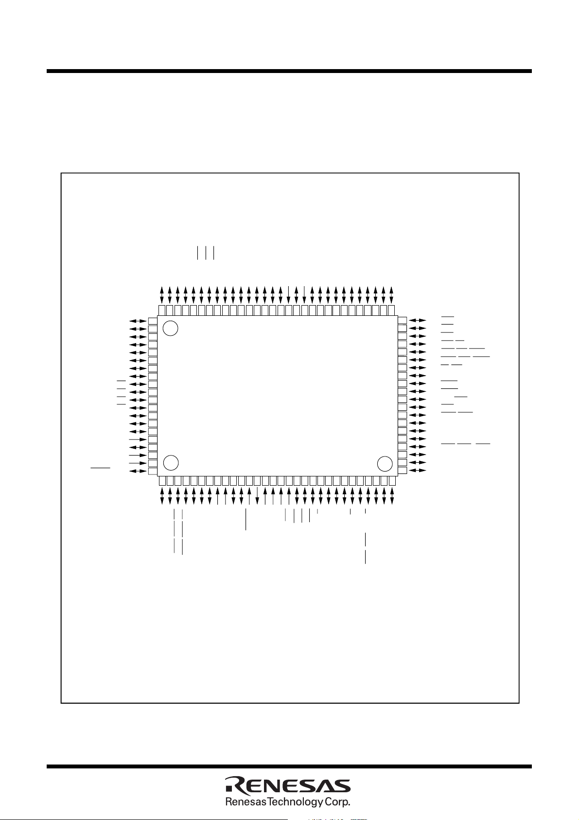
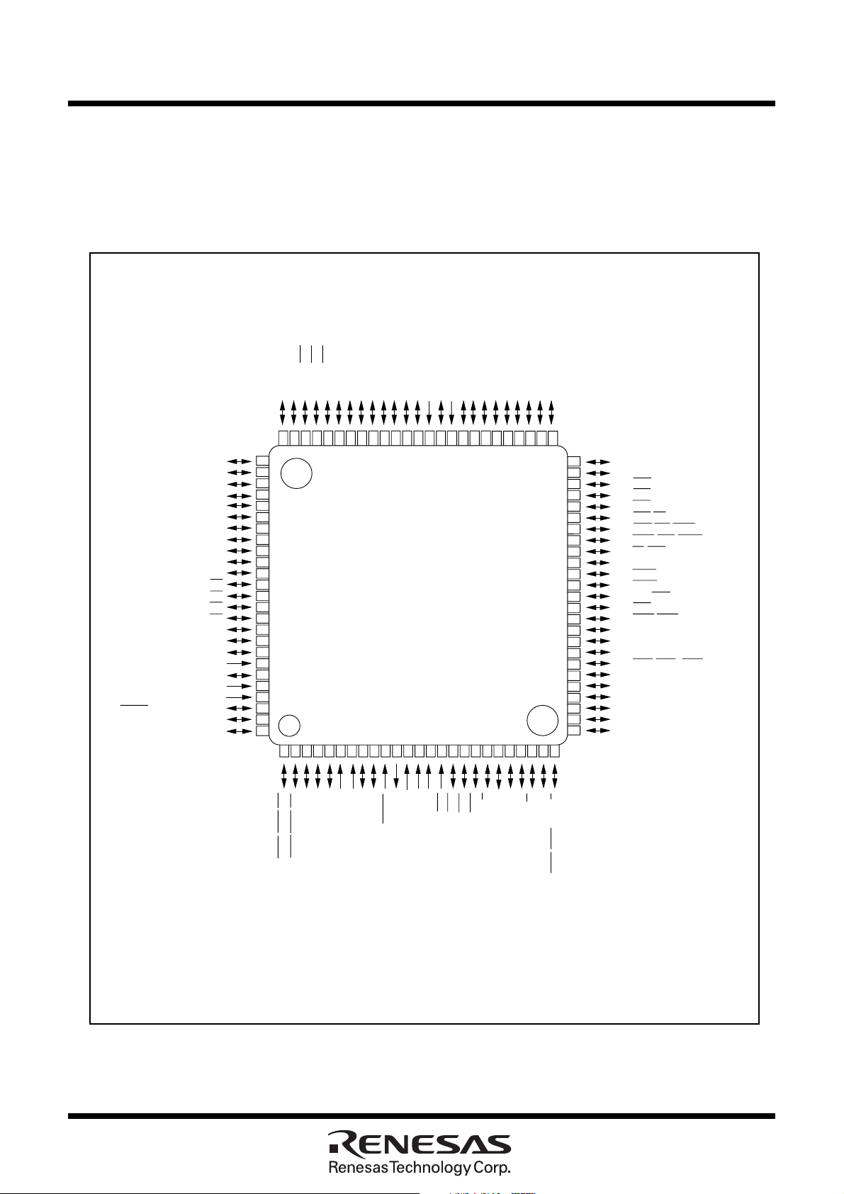
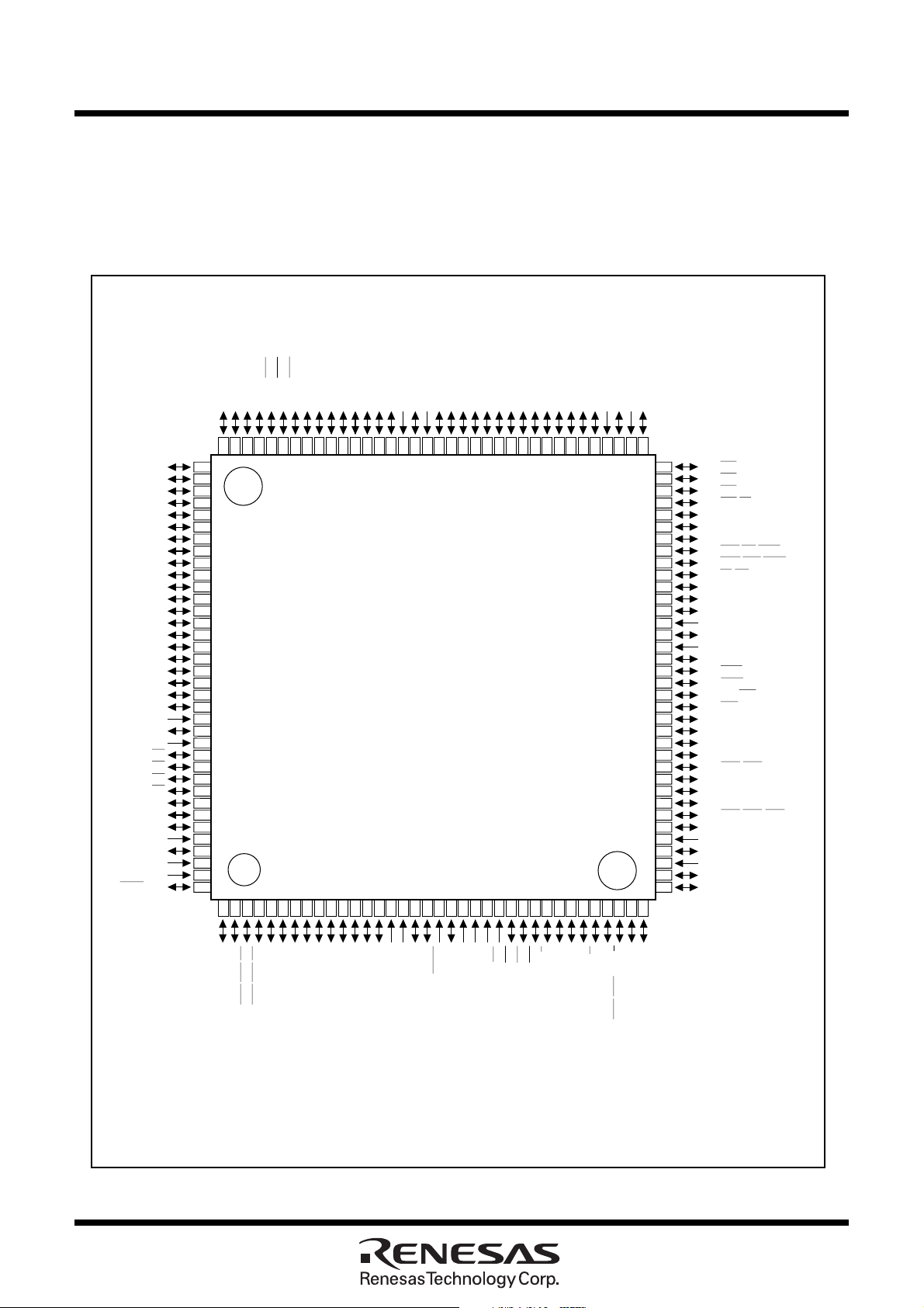
Pin Configuration
Figures 1.1.1 and 1.1.2 show the pin configuration (top view) for 100-pin and Figure 1.1.3 shows the pin
configuration (top view) for 144-pin.
PIN CONFIGURATION (top view)
)
)
)
)
11
12
13
(MA3)(/D
(MA4)(/D
(MA5)(/D
11
12
13
/A
/A
/A
3
4
5
P3
P3
P3
)
15
14
(MA7)(/D
(MA6)(/D
(MA8)
15
14
16
/A
/A
/A
7
6
0
P3
P3
P4
(MA9)
(MA10)
17
18
/A
/A
1
2
P4
P4
(MA11)
19
/A
3
P4
)
)
10
)
9
8
)
)
2
(/D
2
/A
2
P2
)
3
(/D
3
/A
3
P2
)
4
(/D
4
/A
4
P2
)
5
(/D
5
/A
5
P2
)
6
(/D
6
/A
6
P2
7
(/D
7
/A
7
P2
(MA0)(/D
8
/A
0
P3
Vss
(MA1)(/D
9
/A
1
Vcc
P3
(MA2)(/D
10
/A
2
P3
)
)
0
1
/INT5
/INT4
/INT3
(/D
(/D
8
9
10
11
/D
/D
/D
/D
0
1
2
3
P1
P1
P1
P1
15
14
13
12
/D
4
P1
0
1
/A
/D
/A
/D
/D
0
7
1
6
5
P2
P1
P2
P1
P1
515253545556575859606162636465666768697071727374757677787980
P0
7
/D
7
P0
6
/D
P0
5
/D
P0
4
/D
P0
3
/D
P0
2
/D
P0
1
/D
P0
0
/D
P10
7
/AN
7
/KI
P10
6
/AN
6
/KI
P10
5
/AN
5
/KI
P10
4
/AN
4/
KI
P10
3
/AN
P10
2
/AN
P10
1
/AN
AV
SS
P10
0
/AN
V
REF
7
/AD
/SCL
TRG
/R
4
/STxD
AVcc
X
D
P9
81
6
82
5
83
4
84
3
85
2
86
1
87
0
88
3
89
2
90
1
91
0
92
3
93
2
94
1
95
96
0
97
98
99
4
00
1
4
1 2 3 4 5 6 7 8 9 101112131415161718192021222324252627282930
4
4
4
/SS
4
/SRxD
4
/RTS
4
/SDA
/ANEX0/CLK
4
5
D
/CTS
X
P9
IN
/TB4
1
/ANEX1/T
/DA
6
4
P9
P9
M16C/80 Group
3
3
3
3
/SS
3
/RTS
3
/CTS
IN
/TB3
0
/DA
3
P9
/STxD
/SRxD
3
3
/SCL
/SDA
3
3
D
D
X
X
/R
/T
IN
IN
/TB1
/TB2
1
2
P9
P9
/CLK
IN
/TB0
0
P9
BYTE
CNVss
CIN
/X
7
P8
COUT
/X
6
P8
OUT
X
RESET
SS
V
IN
CC
X
V
/NMI
/INT
/INT
5
3
4
P8
P8
P8
/INT
2
P8
/U
IN
/TA4
1
P8
/U
OUT
/TA4
0
P8
IN
/TA3
7
P7
OUT
/TA3
6
P7
/W
IN
/TA2
5
P7
/W
OUT
/TA2
4
P7
/V
IN
/TA1
2
/RTS
2
/CTS
3
P7
/V
OUT
/TA1
2
/CLK
2
P7
(Note)
IN
/TB5
IN
/TA0
2
/SCL
2
/RxD
1
P7
(Note)
OUT
/TA0
2
/SDA
2
D
X
/T
0
P7
1
0
2
P4
4
/CS3/A
20
50
P4
49
48
P4
47
P4
46
P5
45
P5
44
P5
43
P5
42
P5
41
P5
40
P5
39
P5
38
P6
37
P6
36
P6
35
P6
34
P6
33
P6
32
P6
31
P6
(MA12)
5
/CS2/A
21
6
/CS1/A
22
7
/CS0/A
23
0
/WRL/WR/CASL
1
/WRH/BHE/CASH
2
/RD/DW
3
/BCLK/ALE/CLK
4
/HLDA/ALE
5
/HOLD
6
/ALE/RAS
7
/RDY
0
/CTS
0
/RTS
1
/CLK
2
/RxD
3
/T
4
/CTS
5
/CLK
6
/RxD
7
/T
0
0
0
X
D
0
1
/RTS
1
/CTS
1
1
X
D
1
OUT
0
/CLKS
1
Figure 1.1.1. Pin configuration for 100-pin version (top view) (1)
2
Note: This port is N-channel open drain output.
Package: 100P6S-A
Under
development
Description
PIN CONFIGURATION (top view)
P97/AD
TRG/RXD4
P96/ANEX1/TXD4/SDA4/SRxD
Preliminary Specifications REV.D
Specifications in this manual are tentative and subject to change.
)
)
)
10
P12/D
P11/D
P10/D
P07/D
P06/D
P05/D
P04/D
P03/D
P02/D
P01/D
P00/D
P107/AN7/KI
P106/AN6/KI
P105/AN5/KI
P104/AN4/KI
P103/AN
P102/AN
P101/AN
AV
P100/AN
V
AVcc
/SCL4/STxD
P95/ANEX0/CLK
REF
)
8
3
4
5
)
)
0
/INT
11
12
13
/D
/D
/D
3
4
5
P1
P1
P1
10
SS
76
9
77
8
78
79
7
6
80
5
81
4
82
83
3
2
84
1
85
0
86
3
87
2
88
1
89
0
90
3
91
2
92
93
1
94
95
0
96
97
98
4
99
4
00
1
4
1 2 3 4 5 6 7 8 9 10111213141516171819202122232425
1
/INT
/INT
(/D
(/D
0
14
15
1
/A
/A
/D
/D
0
1
6
7
P2
P2
P1
P1
M16C/80 Group
)
2
(/D
2
/A
2
P2
)
3
(/D
3
/A
3
P2
)
4
(/D
4
/A
4
P2
)
5
(/D
5
/A
5
P2
)
6
(/D
6
/A
6
P2
)
7
(/D
7
/A
7
P2
(MA0)(/D
8
/A
0
P3
Vss
9
(MA1)(/D
9
/A
1
Vcc
P3
11
(MA2)(/D
(MA3)(/D
10
11
/A
/A
2
3
P3
P3
Mitsubishi Microcomputers
M16C/80 group
SINGLE-CHIP 16-BIT CMOS MICROCOMPUTER
)
)
)
)
14
12
13
15
(MA6)(/D
(MA8)
(MA7)(/D
14
15
/A
/A
6
7
P3
P3
16
/A
0
P4
51525354555657585960616263646566676869707172737475
(MA9)
17
/A
1
P4
50
49
48
47
46
45
44
43
42
41
40
39
38
37
36
35
34
33
32
31
30
29
28
27
26
P42/A18(MA10)
P4
3/A19
(MA11)
P44/CS3/A20(MA12)
P45/CS2/A
P46/CS1/A
P47/CS0/A
21
22
23
P50/WRL/WR/CASL
P51/WRH/BHE/CASH
P52/RD/DW
P53/BCLK/ALE/CLK
P54/HLDA/ALE
P55/HOLD
P56/ALE/RAS
P57/RDY
P60/CTS0/RTS
P61/CLK
0
P62/RxD
0
P63/TXD
0
P64/CTS1/RTS1/CTS0/CLKS
P65/CLK
1
P66/RxD
1
P67/TXD
1
P70/TXD2/SDA2/TA0
1
/RxD2/SCL2/TA0IN/TB5
P7
P72/CLK2/TA1
0
OUT
OUT
OUT
(Note)
/V
(MA4)(/D
(MA5)(/D
12
13
/A
/A
4
5
P3
P3
IN
1
(Note)
3
3
3
4
/SS
4
/RTS
4
/CTS
IN
/TB4
1
/DA
4
P9
/SS
3
/RTS
3
/CTS
IN
/TB3
0
/DA
3
P9
/STxD
/SRxD
3
3
/SCL
/SDA
3
3
D
D
X
X
/R
/T
IN
IN
/TB1
/TB2
1
2
P9
P9
3
/CLK
IN
/TB0
0
P9
BYTE
CNVss
CIN
/X
7
P8
COUT
/X
6
P8
OUT
X
RESET
IN
SS
CC
X
V
V
/NMI
5
P8
0
1
2
/INT
4
P8
/INT
3
P8
/INT
2
P8
/U
IN
/TA4
1
P8
/U
OUT
/TA4
0
P8
Note: This port is N-channel open drain output.
Figure 1.1.2. Pin configuration for 100-pin version (top view) (2)
IN
/TA3
7
P7
/V
/W
/W
OUT
IN
IN
OUT
/TA3
/TA1
/TA2
6
2
5
/TA2
4
P7
P7
/RTS
P7
2
/CTS
3
P7
Package: 100P6Q-A
3
Under
1
)
)
Preliminary Specifications REV.D
development
Description
Specifications in this manual are tentative and subject to change.
Mitsubishi Microcomputers
M16C/80 group
SINGLE-CHIP 16-BIT CMOS MICROCOMPUTER
PIN CONFIGURATION (top view)
)
0
/INT3
/INT5
/INT4
(/D
13
P10/D8
P07/D7
P06/D6
P05/D5
P04/D4
P114
P113
P112
P111
P110
P03/D3
P02/D2
P01/D1
P00/D0
P157
P156
P155
P154
P153
P152
P151
VSS
P150
VCC
P107/AN7/KI3
P106/AN6/KI2
P105/AN5/KI1
P104/AN4/KI0
P103/AN3
P102/AN2
P101/AN1
AVSS
P100/AN0
VREF
AVCC
P97/ADTRG/RXD4
/SCL4/STxD4
10
/D
/D12
/D9
/D11
2
4
1
3
P1
P1
P1
P1
109
110
111
112
113
114
115
116
117
118
119
120
121
122
123
124
125
126
127
128
129
130
131
132
133
134
135
136
137
138
139
140
141
142
143
144
123 4 76 8 9 101112 13141516 17181920212223 242526272829305 31 32 33 34 35 36
0
/D
/D15
/D14
/A
5
7
6
0
P1
P1
P1
P2
)
8
)
)
(/D1
(/D2
1
2
/A
/A
1
2
P2
P2
100101102103104105106107108
)
)
)
)
)
7
4
(/D6
(/D3
(/D5
(/D
(/D
3
5
4
/A
/A
/A
3
5
4
P2
P2
P2
(MA0)(/D
6
7
8
1
0
/A
/A
/A
6
7
0
SS
P2
V
P2
P3
2
CC
V
P12
P12
P12
M16C/80 Group
3
P12
4
P12
10
)
9
(MA2)(/D
(MA1)(/D
10
9
/A
/A
2
1
P3
P3
)
12
11
(MA4)(/D
(MA3)(/D
12
11
/A
/A
4
3
P3
P3
)
)
14
13
(MA6)(/D
(MA5)(/D
14
13
/A
/A
6
5
P3
P3
)
15
(MA8)
(MA7)(/D
16
15
/A
/A
0
7
P4
P3
78
(MA9)
17
/A
1
P4
SS
V
(MA10)
18
/A
2
CC
P4
V
(MA11)
19
/A
3
P4
7374757677798081828384858687888990919293949596979899
P44/CS3/A20(MA12)
72
P45/CS2/A21
71
P46/CS1/A22
70
P47/CS0/A23
69
P125
68
P126
67
P127
66
P50/WRL/WR/CASL
65
P51/WRH/BHE/CASH
64
P52/RD/DW
63
P53/BCLK/ALE/CLKOUT
62
P130
61
P131
60
VCC
59
P132
58
VSS
57
P133
56
P54/HLDA/ALE
55
P55/HOLD
54
P56/ALE/RAS
53
P57/RDY
52
P134
51
P135
50
P136
49
P137
48
P60/CTS0/RTS0
47
P61/CLK0
46
P62/RXD0
45
P63/TXD0
44
P64/CTS1/RTS1/CTS0/CLKS
43
P65/CLK1
42
VSS
41
40
P66/RXD1
VCC
39
38
P67/TXD1
P70/TXD2/SDA2/TA0OUT
37
4
2
4
4
/CLK
0
/SRxD
4
/SDA
/ANEX
4
5
D
X
P9
/T
/ANEX1
6
P9
4
/SS
4
/RTS
4
/CTS
4IN
/TB
/DA1
4
P9
3
/SS
3
/RTS
3
/CTS
3IN
/TB
/DA0
3
P9
3
3
/STxD
/SRxD
3
3
/SCL
/SDA
3
3
D
D
X
/RX
/T
1IN
2IN
/TB
/TB
1
2
P9
P9
/CLK3
0IN
/TB
0
P9
6
P14
5
P14
P14
3
P14
P14
1
P14
0
P14
BYTE
SS
CNV
CIN
COUT
/X
7
/X
6
P8
P8
XOUT
RESET
XIN
VSS
VCC
Figure 1.1.3. Pin configuration for 144-pin version (top view)
4
/NMI
5
P8
2
/INT
4
P8
1
/INT
3
P8
0
/INT
2
P8
/U
4IN
/TA
1
P8
/U
4OUT
/TA
0
P8
3IN
/TA
7
P7
3OUT
/TA
6
P7
/W
2IN
/TA
5
P7
/W
2OUT
/TA
4
P7
/V
1IN
/TA
2
/RTS
2
/CTS
3
P7
(Note)
/V
1OUT
/TA
2
/CLK
2
P7
(Note)
5IN
/TB
0IN
/TA
2
/SCL
2
D
X
/R
1
P7
Note: This port is N-channel open drain output.
Package: 144P6Q-A
Under
A
A
A
A
development
Description
Specifications in this manual are tentative and subject to change.
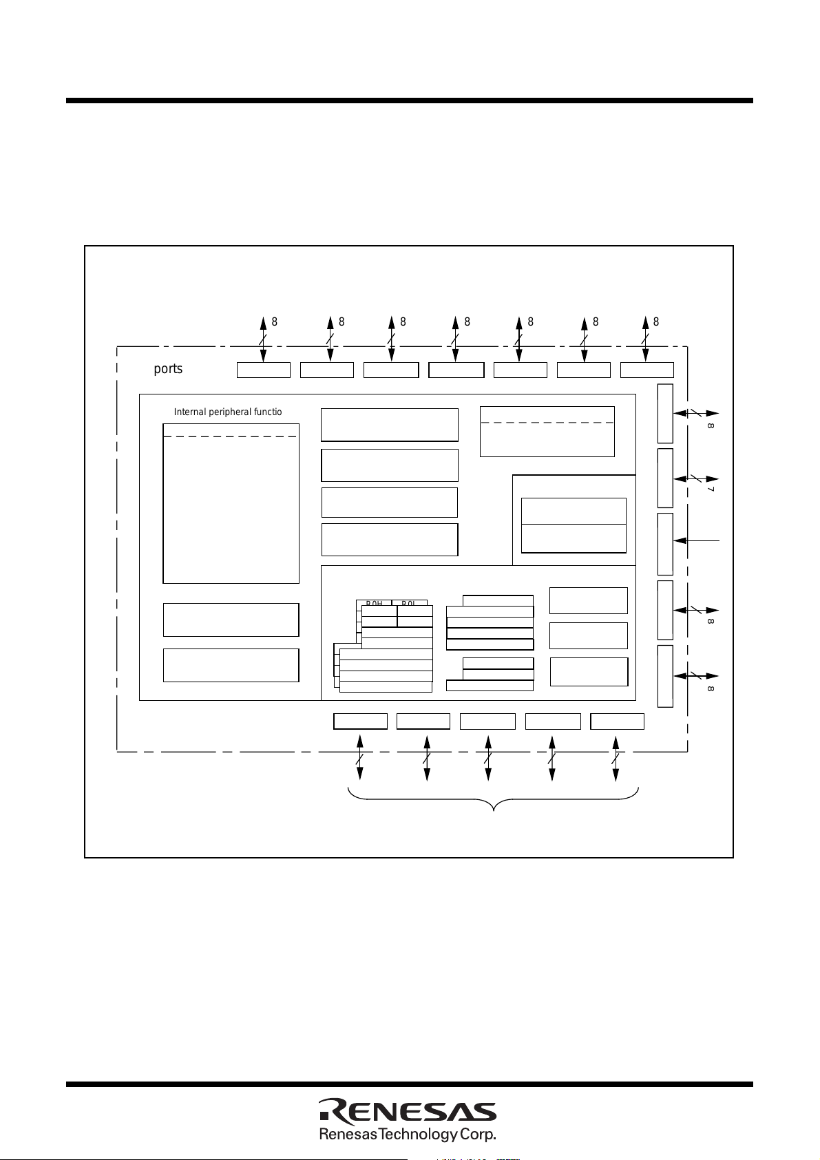
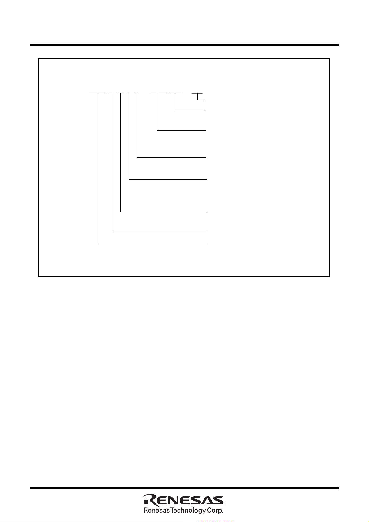
Block Diagram
Figure 1.1.4 is a block diagram of the M16C/80 group.
8888888
Preliminary Specifications REV.D
Mitsubishi Microcomputers
M16C/80 group
SINGLE-CHIP 16-BIT CMOS MICROCOMPUTER
I/O ports
Port P0
Internal peripheral functions
Timer
Timer TA0 (16 bits)
Timer TA1 (16 bits)
Timer TA2 (16 bits)
Timer TA3 (16 bits)
Timer TA4 (16 bits)
Timer TB0 (16 bits)
Timer TB1 (16 bits)
Timer TB2 (16 bits)
Timer TB3 (16 bits)
Timer TB4 (16 bits)
Timer TB5 (16 bits)
Watchdog timer
(15 bits)
D-A converter
(8 bits X 2 channels)
Port P1
Expandable up to 10 channels)
UART /clock synchronous SI/O
CRC arithmetic circuit (CCITT)
Port P2
A-D converter
(10 bits X 8 channels
(8 bits X 5 channels)
X-Y converter
(16 bits X 16 bits)
Registers
R0LR0H
R0H R0L
R1H R1L
R2
R2
R3
A0
A1
FB
SB
Port P14
1216 5
(Polynomial : X +X +X +1)
M16C/80 series 16-bit CPU core
R1H R1L
Port P15
Port P3
Port P4
System clock generator
XIN - XOUT
XCIN - XCOUT
AAAAA
AAAAA
AAAAA
FLG
INTB
ISP
USP
PC
SVF
SVP
VCT
Port P13
Port P12
Port P5
Memory
ROM
(Note 1)
RAM
(Note 2)
DRAM
controller
DRAM
controller
Multiplier
AA
Port P6
Port P7
8
Port P8
7
Port P8
5
Port P9
8
Port P10
8
Port P11
Note 1: ROM size depends on MCU type.
Note 2: RAM size depends on MCU type.
Note 3: Ports P11 to P15 exist in 144-pin version.
Figure 1.1.4. Block diagram of the M16C/80 group
87885
(Note 3)
5
Under
development
Description
Preliminary Specifications REV.D
Specifications in this manual are tentative and subject to change.
SINGLE-CHIP 16-BIT CMOS MICROCOMPUTER
Mitsubishi Microcomputers
M16C/80 group
Performance Outline
Table 1.1.1 is a performance outline of M16C/80 group.
Table 1.1.1. Performance outline of M16C/80 group
Item Performance
Number of basic instructions 106 instructions
Shortest instruction execution time 50ns(f(XIN)=20MHz)
Memory See ROM expansion figure.
capacity 10 to 24 K bytes
I/O port P0 to P10 (except P85) 8-bit x 10, 7-bit x 1
Input port 1 bit x 1
Multifunction 16 bits x 5
timer 16 bits x 6
Serial I/O (UART or clock synchronous) x 5
A-D converter 10 bits x (8 + 2) channels
D-A converter 8 bits x 2
DMAC 4 channels
DRAM controller CAS before RAS refresh, self-refresh, EDO, FP
CRC calculation circuit CRC-CCITT
X-Y converter 16 bits X 16 bits
Watchdog timer 15 bits x 1 (with prescaler)
Interrupt 29 internal and 8 external sources, 5 software sources, 7
Clock generating circuit 2 built-in clock generation circuits
Supply voltage 4.2 to 5.5V (f(XIN)=20MHz) Mask ROM, external ROM
Power consumption 45mA (f(XIN) = 20MHz without software wait,Vcc=5V)
I/O 5V
characteristics 5mA
Memory expansion Available (up to 16M bytes)
Operating ambient temperature –40 to 85oC
Device configuration CMOS high performance silicon gate
Package 100-pin and 144-pin plastic mold QFP
ROM
RAM
100-pin
144-pin
P85
TA0, TA1, TA2, TA3,TA4
TB0, TB1, TB2, TB3, TB4, TB5
UART0, UART1, UART2,
UART3, UART4
I/O withstand voltage
Output current
P0 to P15 (except P85) 8-bit x 13, 7-bit x 2, 5-bit x 1
levels
(built-in feedback resistance, and external ceramic or
quartz oscillator)
and flash memory versions
2.7 to 5.5V (f(XIN)=10MHz) Mask ROM, external ROM
and flash memory versions
Mask ROM 128 Kbytes version
6
Under
development
Description
Specifications in this manual are tentative and subject to change.
SINGLE-CHIP 16-BIT CMOS MICROCOMPUTER
Mitsubishi plans to release the following products in the M16C/80 group:
(1) Support for mask ROM version, external ROM version and flash memory version
(2) ROM capacity
(3) Package
100P6S-A : Plastic molded QFP (mask ROM version and flash memory version)
100P6Q-A : Plastic molded QFP (mask ROM version and flash memory version)
144P6Q-A : Plastic molded QFP (mask ROM version and flash memory version)
ROM Size
(Byte)
M30805SGP-BL
M30803SFP/GP-BL
Preliminary Specifications REV.D
External
ROM
M30802SGP-BL
M30800SFP/GP-BL
M30805SGP
M30803SFP/GP
M30802SGP
M30800SFP/GP
Mitsubishi Microcomputers
M16C/80 group
256K
128K
M30803MG-XXXFP/GP
M30805MG-XXXGP
M30800MC-XXXFP/GP
M30802MC-XXXGP
Mask ROM version
M30803FGFP/GP
M30805FGGP
M30800FCFP/GP
M30802FCGP
Flash memory
version
External ROM version
Figure 1.1.5. ROM expansion
The M16C/80 group products currently supported are listed in Table 1.1.2.
Table 1.1.2. M16C/80 group
Type No
M30800MC-XXXFP
M30800MC-XXXGP
M30802MC-XXXGP
M30803MG-XXXFP
M30803MG-XXXGP
M30805MG-XXXGP
M30800FCFP
M30800FCGP
M30802FCGP
M30803FGFP
M30803FGGP
M30805FGGP
M30800SFP
M30800SGP
M30802SGP
M30803SFP
M30803SGP
M30805SGP
M30800SFP-BL
M30800SGP-BL
M30802SGP-BL
M30803SFP-BL
M30803SGP-BL
M30805SGP-BL
*
: New product
ROM capacity
128K bytes
256K bytes
128K bytes
256K bytes
*
RAM capacity
10K bytes 100P6S-A
20K bytes
10K bytes
20K bytes
10K bytes
*
*
24K bytes
*
*
10K bytes
*
*
*
24K bytes
*
*
Package type
100P6Q-A
144P6Q-A
100P6S-A
100P6Q-A
144P6Q-A
100P6S-A
100P6Q-A
144P6Q-A
100P6S-A
100P6Q-A
144P6Q-A
100P6S-A
100P6Q-A
144P6Q-A
100P6S-A
100P6Q-A
144P6Q-A
100P6S-A
100P6Q-A
144P6Q-A
100P6S-A
100P6Q-A
144P6Q-A
As of August, 2001
Remarks
Mask ROM version
Flash memory version
External ROM version
External ROM version
with built-in boot loader
7
Under
development
Description
Type No. M 3 0 8 0 2 M C – X X X G P – BL
Preliminary Specifications REV.D
Specifications in this manual are tentative and subject to change.
Boot loader
Package type:
FP : Package 100P6S-A
GP : Package 100P6Q-A, 144P6Q-A
ROM No.
Omitted for blank external ROM version
and flash memory version
ROM capacity:
C : 128K bytes
G : 256K bytes
Memory type:
M : Mask ROM version
S : External ROM version
F : Flash memory version
Mitsubishi Microcomputers
M16C/80 group
SINGLE-CHIP 16-BIT CMOS MICROCOMPUTER
Figure 1.1.6. Type No., memory size, and package
Shows RAM capacity, pin count, etc
(The value itself has no specific meaning)
M16C/80 Group
M16C Family
8
Under
development
Pin Description
Specifications in this manual are tentative and subject to change.
Pin Description (1)
Preliminary Specifications REV.D
Mitsubishi Microcomputers
M16C/80 group
SINGLE-CHIP 16-BIT CMOS MICROCOMPUTER
Pin name
VCC, V
CNV
SS
RESET
X
IN
X
OUT
BYTE
AV
CC
AV
SS
V
REF
SS
Signal name
Power supply
input
CNV
SS
Reset input
Clock input
Clock output
External data
bus width
select input
Analog power
supply input
Analog power
supply input
Reference
voltage input
I/O type
I
I
I
O
I
I
Function
CC
Supply 4.2 (2.7) to 5.5 V to the V
This pin switches between processor modes. Connect it to the V
pin. Supply 0 V to the VSS pin.
SS
when operating in single-chip or memory expansion mode after reset.
Connect it to the V
CC
when in microprocessor mode after reset.
An “L” on this input resets the microcomputer.
These pins are provided for the main clock generating circuit. Connect
a ceramic resonator or crystal between the X
use an externally derived clock, input it to the X
X
OUT
pin open.
IN
and the X
IN
pin and leave the
OUT
pins. To
This pin selects the width of an data bus in the external area 3. A 16-
-bit width is selected when this input is “L”; an 8-bit width is selected
when this input is “H”. This input must be fixed to either “H” or “L”.
When not using the external bus, connect this pin to V
SS
.
This pin is a power supply input for the A-D converter. Connect this
pin to V
CC
.
This pin is a power supply input for the A-D converter. Connect this
pin to V
SS
.
This pin is a reference voltage input for the A-D converter.
P00 to P0
D0 to D
7
P10 to P1
D8 to D
15
P20 to P2
A0 to A
7
A0/D0 to
A
P30 to P3
A8 to A
15
A8/D8 to
A
15/D15
7
7
7
7/D7
7
I/O port P0
I/O port P1
I/O port P2
I/O port P3
I/O
This is an 8-bit CMOS I/O port. It has an input/output port direction
register that allows the user to set each pin for input or output
individually. When set for input in single chip mode, the user can
specify in units of four bits via software whether or not they are tied to
a pull-up resistance. In memory expansion and microprocessor
mode, an built-in pull-up resistance cannot be used. However, it is
possible to select pull-up resistance presence to the usable port as I/
O port by setting.
When set as a separate bus, these pins input and output data (D
I/O
This is an 8-bit I/O port equivalent to P0. P1
I/O
5
to P17 also function as
external interrupt pins as selected by software.
When set as a separate bus, these pins input and output data
I/O
This is an 8-bit I/O port equivalent to P0.
I/O
0–A7
O
These pins output 8 low-order address bits (A
If a multiplexed bus is set, these pins input and output data (D
I/O
and output 8 low-order address bits (A
0–A7
).
) separated in time by
multiplexing.
This is an 8-bit I/O port equivalent to P0.
I/O
These pins output 8 middle-order address bits (A
O
If the external bus is set as a 16-bit wide multiplexed bus, these pins
I/O
input and output data (D
bits (A
8–A15
) separated in time by multiplexing.
8–D15
) and output 8 middle-order address
8–A15
0–D7
).
(D8–D15).
0–D7
)
).
MA0 to MA7
If accessing to DRAM area, these pins output row address and
O
column address separated in time by multiplexing.
9
Under
development
Pin Description
Specifications in this manual are tentative and subject to change.
Pin Description (2)
Preliminary Specifications REV.D
Mitsubishi Microcomputers
M16C/80 group
SINGLE-CHIP 16-BIT CMOS MICROCOMPUTER
Signal name FunctionPin name I/O type
P40 to P4
7
A16 to A22,
23
A
0
to CS
CS
3
MA8 to MA12
P5
0
to P5
7
WRL / WR,
WRH / BHE,
RD,
BCLK,
HLDA,
HOLD,
ALE,
RDY
I/O port P4 This is an 8-bit I/O port equivalent to P0.I/O
O
O
O
I/O port P5 I/O
O
O
O
O
O
O
I
These pins output 8 high-order address bits (A
23
address bit (A
) outputs inversely.
16–A22
, A23). Highest
These pins output CS0–CS3 signals. CS0–CS3 are chip select
signals used to specify an access space.
If accessing to DRAM area, these pins output row address and
column address separated in time by multiplexing.
This is an 8-bit I/O port equivalent to P0. P53 in this port outputs a
IN
divide-by-8 or divide-by-32 clock of X
CIN
frequency as X
as selected by software.
or a clock of the same
Output WRL, WRH (WR and BHE), RD, BCLK, HLDA, and ALE
signals. WRL and WRH, and BHE and WR can be switched using
software control.
WRL, WRH, and RD selected
With a 16-bit external data bus, data is written to even addresses
I
when the WRL signal is “L” and to the odd addresses when the
WRH signal is “L”. Data is read when RD is “L”.
WR, BHE, and RD selected
Data is written when WR is “L”. Data is read when RD is “L”. Odd
addresses are accessed when BHE is “L”. Use this mode when
using an 8-bit external data bus.
While the input level at the HOLD pin is “L”, the microcomputer is
placed in the hold state. While in the hold state, HLDA outputs an “L”
level. ALE is used to latch the address. While the input level of the
RDY pin is “L”, the bus of microcomputer is in the wait state.
DW,
CASL,
CASH,
RAS
P60 to P6
P70 to P77
0
to P84,
P8
6
,
P8
7
,
P8
5
P8
P90 to P9
7
7
I/O port P6
I/O port P7
I/O port P8
I/O port P8
I/O port P9
O
O
O
O
I/O
When accessing to DRAM area while DW signal is “L”, write to DRAM.
CASL and CASH show timing when latching to line address. When
CASL accesses to even address, and CASH to odd, these two pins
become “L”. RAS signal shows timing when latching to row address.
This is an 8-bit I/O port equivalent to P0. When set for input in single
chip mode, microprocessor mode and memory expansion mode the
user can specify in units of four bits via software whether or not they
are tied to a pull-up resistance. Pins in this port also function as
UART0 and UART1 I/O pins as selected by software.
0
I/O
This is an 8-bit I/O port equivalent to P6 (P7
open drain output). Pins in this port also function as timer A
and P71 are N-channel
0–A3
,
timer B5 or UART2 I/O pins as selected by software.
I/O
I/O
I/O
5
P80 to P84, P86, and P87 are I/O ports with the same functions as P6.
Using software, they can be made to function as the I/O pins for timer
6
A4 and the input pins for external interrupts. P8
and P87 can be set
using software to function as the I/O pins for a sub clock generation
circuit. In this case, connect a quartz oscillator between P8
I
pin) and P8
7
(X
CIN
pin). P85 is an input-only port that also functions
6
(X
COUT
for NMI. The NMI interrupt is generated when the input at this pin
changes from “H” to “L”. The NMI function cannot be canceled using
software. The pull-up cannot be set for this pin.
I/O
This is an 8-bit I/O port equivalent to P6. Pins in this port also
function as UART3 and UART4 I/O pins, Timer B0–B4 input pins, D-A
converter output pins, A-D converter extended input pins, or A-D
trigger input pins as selected by software.
P100 to P10
10
7
I/O port P10
I/O
This is an 8-bit I/O port equivalent to P6. Pins in this port also
4
function as A-D converter input pins. Furthermore, P10
–P107 also
function as input pins for the key input interrupt function.
Under
development
Pin Description
Specifications in this manual are tentative and subject to change.
Pin Description (3)
(Note)
Preliminary Specifications REV.D
Mitsubishi Microcomputers
M16C/80 group
SINGLE-CHIP 16-BIT CMOS MICROCOMPUTER
Signal name FunctionPin name I/O type
II/OI/O port P11P110 to P114 This is an 5-bit I/O port equivalent to P6.
0
to P127 This is an 8-bit I/O port equivalent to P6.
(Note)
(Note)
0
to P146 This is an 7-bit I/O port equivalent to P6.
(Note)
(Note)
II/OI/O port P12P12
II/OI/O port P13P130 to P137 This is an 8-bit I/O port equivalent to P6.
II/OI/O port P14P14
II/OI/O port P15P150 to P157 This is an 8-bit I/O port equivalent to P6.
Note : Port P11 to P15 exist in 144-pin version.
11
Under
A
A
development
Memory
Preliminary Specifications REV.D
Specifications in this manual are tentative and subject to change.
SINGLE-CHIP 16-BIT CMOS MICROCOMPUTER
Mitsubishi Microcomputers
M16C/80 group
Operation of Functional Blocks
The M16C/80 group accommodates certain units in a single chip. These units include ROM and RAM to
store instructions and data and the central processing unit (CPU) to execute arithmetic/logic operations.
Also included are peripheral units such as timers, serial I/O, D-A converter, DMAC, CRC calculation circuit,
A-D converter, DRAM controller and I/O ports.
The following explains each unit.
Memory
Figure 1.2.1 is a memory map of the M16C/80 group. The address space extends the 16 Mbytes from
address 00000016 to FFFFFF16. From FFFFFF16 down is ROM. For example, in the M30800MC-XXXFP,
there is 128K bytes of internal ROM from FE000016 to FFFFFF16. The vector table for fixed interrupts such
as the reset and NMI are mapped to FFFFDC16 to FFFFFF16. The starting address of the interrupt routine
is stored here. The address of the vector table for timer interrupts, etc., can be set as desired using the
internal register (INTB). See the section on interrupts for details.
From 00040016 up is RAM. For example, in the M30800MC-XXXFP, 10 Kbytes of internal RAM is mapped
to the space from 00040016 to 002BFF16. In addition to storing data, the RAM also stores the stack used
when calling subroutines and when interrupts are generated.
The SFR area is mapped to 00000016 to 0003FF16. This area accommodates the control registers for
peripheral devices such as I/O ports, A-D converter, serial I/O, and timers, etc. Figure 1.5.1 to 1.5.4 are
location of peripheral unit control registers. Any part of the SFR area that is not occupied is reserved and
cannot be used for other purposes.
The special page vector table is mapped to FFFE0016 to FFFFDB16. If the starting addresses of subroutines or the destination addresses of jumps are stored here, subroutine call instructions and jump instructions can be used as 2-byte instructions, reducing the number of program steps.
In memory expansion mode and microprocessor mode, a part of the spaces are reserved and cannot be
used. For example, in the M30800MC-XXXFP, the following spaces cannot be used.
• The space between 002C0016 and 00800016 (Memory expansion and microprocessor modes)
• The space between F0000016 and FDFFFF16 (Memory expansion mode)
_______
<100-pin version>
Type No.
M30800MC/FC
M30803MG/FG
<144-pin version>
Type No.
M30802MC/FC
M30805MG/FG
M30802S
M30805S
Address
XXXXX
002BFF
0053FF
Address
XXXXX
002BFF
0053FF
002BFF
0063FF
Figure 1.2.1. Memory map
12
000000
16
000400
16
XXXXXX
Address
YYYYY
FE0000
FC0000
Address
YYYYY
FE0000
FC0000
16
16
16
16
16
16
16
16
16
008000
16
16
16
F00000
16
YYYYYY
16
16
16
FFFFFF
Note 1: During memory expansion and microprocessor modes, can not be used.
Note 2: In memory expansion mode, can not be used.
SFR area
For details, see
Figures 1.5.1 to
Internal RAM
16
Internal reserved
area (Note 1)
AAA
External area
AAA
Internal reserved
area (Note 2)
16
Internal ROM
16
1.5.4
area
area
FFFE00
FFFFDC
FFFFFF
16
Special page
vector table
16
Undefined instruction
Overflow
BRK instruction
Address match
Watchdog timer
16
Reset
NMI
Under
development
CPU
Preliminary Specifications REV.D
Specifications in this manual are tentative and subject to change.
SINGLE-CHIP 16-BIT CMOS MICROCOMPUTER
Mitsubishi Microcomputers
M16C/80 group
Central Processing Unit (CPU)
The CPU has a total of 28 registers shown in Figure 1.3.1. Eight of these registers (R0, R1, R2, R3, A0, A1,
SB and FB) come in two sets; therefore, these have two register banks.
General register
b31
R2
R3
b23
High-speed interrupt register
b23
b15 b0
FLG
R0H
R1H
A0
A1
SB
FB
USP
ISP
INTB
PC
b15 b0
SVP
R0L
R1L
R2
R3
SVF
Flag register
Data register (Note)
Address register (Note)
Static base register (Note)
Frame base register (Note)
User stack pointer
Interrupt stack pointer
Interrupt table register
Program counter
Flag save register
PC save register
VCT
DMAC related register
b15
b23
DMA0
DMA1
DSA0
DSA1
DRA0
DRA1
Note: These registers have two register banks.
Figure 1.3.1. Central processing unit register
b7 b0
DMD0
DMD1
DCT0
DCT1
DRC0
DRC1
Vector register
DMA mode register
DMA transfer count register
DMA transfer count reload register
DMA memory address register
DMA SFR address register
DMA memory address reload register
13

Under
development
CPU
Preliminary Specifications REV.D
Specifications in this manual are tentative and subject to change.
SINGLE-CHIP 16-BIT CMOS MICROCOMPUTER
Mitsubishi Microcomputers
M16C/80 group
(1) Data registers (R0, R0H, R0L, R1, R1H, R1L, R2, R3, R2R0 and R3R1)
Data registers (R0, R1, R2, and R3) are configured with 16 bits, and are used primarily for transfer and
arithmetic/logic operations.
Registers R0 and R1 each can be used as separate 8-bit data registers, high-order bits as (R0H/R1H),
and low-order bits as (R0L/R1L). Registers R2 and R0, as well as R3 and R1 can use as 32-bit data
registers (R2R0/R3R1).
(2) Address registers (A0 and A1)
Address registers (A0 and A1) are configured with 24 bits, and have functions equivalent to those of data
registers. These registers can also be used for address register indirect addressing and address register
relative addressing.
(3) Static base register (SB)
Static base register (SB) is configured with 24 bits, and is used for SB relative addressing.
(4) Frame base register (FB)
Frame base register (FB) is configured with 24 bits, and is used for FB relative addressing.
(5) Program counter (PC)
Program counter (PC) is configured with 24 bits, indicating the address of an instruction to be executed.
(6) Interrupt table register (INTB)
Interrupt table register (INTB) is configured with 24 bits, indicating the start address of an interrupt vector
table.
(7) User stack pointer (USP), interrupt stack pointer (ISP)
Stack pointer comes in two types: user stack pointer (USP) and interrupt stack pointer (ISP), each configured with 24 bits.
Your desired type of stack pointer (USP or ISP) can be selected by a stack pointer select flag (U flag).
This flag is located at the position of bit 7 in the flag register (FLG).
Set USP and ISP to an even number so that execution efficiency is increased.
(8) Save flag register (SVF)
This register consists of 16 bits and is used to save the flag register when a high-speed interrupt is
generated.
14

Under
development
CPU
Preliminary Specifications REV.D
Specifications in this manual are tentative and subject to change.
SINGLE-CHIP 16-BIT CMOS MICROCOMPUTER
Mitsubishi Microcomputers
M16C/80 group
(9) Save PC register (SVP)
This register consists of 24 bits and is used to save the program counter when a high-speed interrupt is
generated.
(10) Vector register (VCT)
This register consists of 24 bits and is used to indicate the jump address when a high-speed interrupt is
generated.
(11) DMA mode registers (DMD0/DMD1)
These registers consist of 8 bits and are used to set the transfer mode, etc. for DMA.
(12) DMA transfer count registers (DCT0/DCT1)
These registers consist of 16 bits and are used to set the number of DMA transfers performed.
(13) DMA transfer count reload registers (DRC0/DRC1)
These registers consist of 16 bits and are used to reload the DMA transfer count registers.
(14) DMA memory address registers (DMA0/DMA1)
These registers consist of 24 bits and are used to set a memory address at the source or destination of
DMA transfer.
(15) DMA SFR address registers (DSA0/DSA1)
These registers consist of 24 bits and are used to set a fixed address at the source or destination of DMA
transfer.
(16) DMA memory address reload registers (DRA0/DRA1)
These registers consist of 24 bits and are used to reload the DMA memory address registers.
15

Under
development
Preliminary Specifications REV.D
Specifications in this manual are tentative and subject to change.
CPU
(17) Flag register (FLG)
Flag register (FLG) is configured with 11 bits, each bit is used as a flag. Figure 1.3.2 shows the flag
register (FLG). The following explains the function of each flag:
• Bit 0: Carry flag (C flag)
This flag retains a carry, borrow, or shift-out bit that has occurred in the arithmetic/logic unit.
• Bit 1: Debug flag (D flag)
This flag enables a single-step interrupt.
When this flag is “1”, a single-step interrupt is generated after instruction execution. This flag is
cleared to “0” when the interrupt is acknowledged.
• Bit 2: Zero flag (Z flag)
This flag is set to “1” when an arithmetic operation resulted in 0; otherwise, cleared to “0”.
Mitsubishi Microcomputers
M16C/80 group
SINGLE-CHIP 16-BIT CMOS MICROCOMPUTER
• Bit 3: Sign flag (S flag)
This flag is set to “1” when an arithmetic operation resulted in a negative value; otherwise, cleared
to “0”.
• Bit 4: Register bank select flag (B flag)
This flag chooses a register bank. Register bank 0 is selected when this flag is “0” ; register bank
1 is selected when this flag is “1”.
• Bit 5: Overflow flag (O flag)
This flag is set to “1” when an arithmetic operation resulted in overflow; otherwise, cleared to “0”.
• Bit 6: Interrupt enable flag (I flag)
This flag enables a maskable interrupt.
An interrupt is disabled when this flag is “0”, and is enabled when this flag is “1”. This flag is
cleared to “0” when the interrupt is acknowledged.
• Bit 7: Stack pointer select flag (U flag)
Interrupt stack pointer (ISP) is selected when this flag is “0” ; user stack pointer (USP) is selected
when this flag is “1”.
This flag is cleared to “0” when a hardware interrupt is acknowledged or an INT instruction of
software interrupt Nos. 0 to 31 is executed.
16
• Bits 8 to 11: Reserved area
Under
development
CPU
Preliminary Specifications REV.D
Specifications in this manual are tentative and subject to change.
SINGLE-CHIP 16-BIT CMOS MICROCOMPUTER
Mitsubishi Microcomputers
M16C/80 group
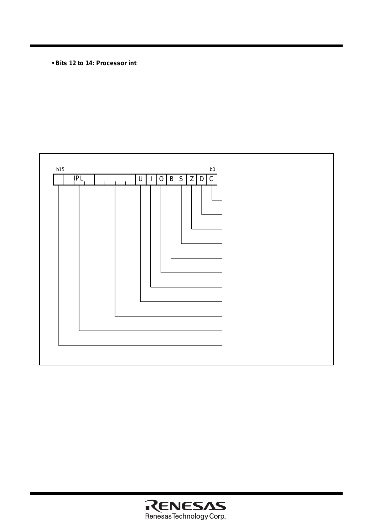
• Bits 12 to 14: Processor interrupt priority level (IPL)
Processor interrupt priority level (IPL) is configured with three bits, for specification of up to eight
processor interrupt priority levels from level 0 to level 7.
If a requested interrupt has priority greater than the processor interrupt priority level (IPL), the interrupt
is enabled.
• Bit 15: Reserved area
b0b15
IPL
Flag register (FLG)
CDZSBOIU
Carry flag
Figure 1.3.2. Flag register (FLG)
Debug flag
Zero flag
Sign flag
Register bank select flag
Overflow flag
Interrupt enable flag
Stack pointer select flag
Reserved area
Processor interrupt priority level
Reserved area
17
Under
development
Reset
Preliminary Specifications REV.D
Specifications in this manual are tentative and subject to change.
SINGLE-CHIP 16-BIT CMOS MICROCOMPUTER
Mitsubishi Microcomputers
M16C/80 group
Reset
There are two kinds of resets; hardware and software. In both cases, operation is the same after the reset.
(See “Software Reset” for details of software resets.) This section explains on hardware resets.
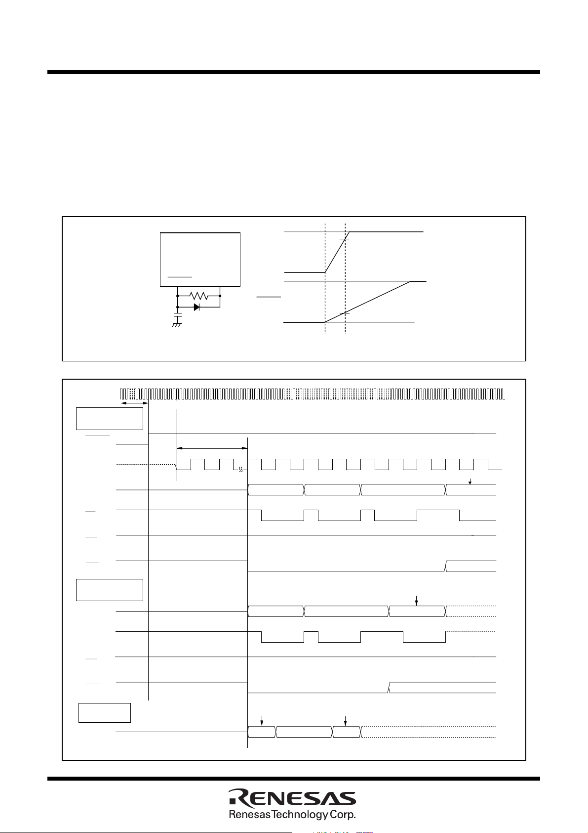
When the supply voltage is in the range where operation is guaranteed, a reset is effected by holding the
reset pin level “L” (0.2VCC max.) for at least 20 cycles. When the reset pin level is then returned to the “H”
level while main clock is stable, the reset status is cancelled and program execution resumes from the
address in the reset vector table.
Figure 1.4.1 shows the example reset circuit. Figure 1.4.2 shows the reset sequence.
RESET
Example when f(XIN) = 10MHz and V
V
Figure 1.4.1. Example reset circuit
X
IN
More than 20 cycles are needed
Microprocessor
mode BYTE = “H”
RESET
BCLK
Address
RD
BCLK 24cycles
CC
5V
V
CC
0V
5V
RESET
0V
FFFFC
CC
= 5V
16
4.2V
0.8V
.
Content of reset vector
FFFFD
16
FFFFE
16
WR
CS0
Microprocessor
mode BYTE = “L”
Address
RD
WR
CS0
Single chip
mode
Address
Figure 1.4.2. Reset sequence
18
FFFFC
FFFFC
16
16
FFFFE
FFFFE
16
Content of reset vector
16
Content of reset vector
Under
development
Reset
Preliminary Specifications REV.D
Specifications in this manual are tentative and subject to change.
Mitsubishi Microcomputers
M16C/80 group
SINGLE-CHIP 16-BIT CMOS MICROCOMPUTER
Table 1.4.1 shows the statuses of the other pins while the RESET pin level is “L”. Figures 1.4.3 and 1.4.4
____________
show the internal status of the microcomputer immediately after the reset is cancelled.
Table 1.4.1. Pin status when RESET pin level is “L”
____________
Status
Pin name
P0
P1
P2, P3, P4
P5
0
P5
1
P5
2
P5
3
P5
4
CNVSS = V
Input port (floating)
Input port (floating)
Input port (floating)
Input port (floating)
Input port (floating)
Input port (floating)
Input port (floating)
Input port (floating)
SS
CNVSS = V
BYTE = V
SS
Data input (floating)
Data input (floating)
Address output (undefined)
WR output (“H” level is output)
BHE output (undefined)
RD output (“H” level is output)
BCLK output
HLDA output (The output value
depends on the input to the
HOLD pin)
CC
BYTE = V
CC
Data input (floating)
Input port (floating)
Address output (undefined)
WR output (“H” level is output)
BHE output (undefined)
RD output (“H” level is output)
BCLK output
HLDA output (The output value
depends on the input to the
HOLD pin)
P5
5
P5
6
P5
7
P6, P7, P80 to P84,
P8
6
, P87, P9, P10,
P11, P12, P13,
P14, P15 (Note)
Input port (floating)
Input port (floating)
Input port (floating)
Input port (floating)
Input port (floating) Input port (floating) Input port (floating)
Note :Port P11 to P15 exist in 144-pin vrsion.
HOLD input (floating)
RAS output
RDY input (floating)
HOLD input (floating)
RAS output
RDY input (floating)
Input port (floating) Input port (floating)
19
Under
development
Reset
Preliminary Specifications REV.D
Specifications in this manual are tentative and subject to change.
Mitsubishi Microcomputers
M16C/80 group
SINGLE-CHIP 16-BIT CMOS MICROCOMPUTER
(1) (0004
(2) (000516)···Processor mode register 1
(3) (0006
(4) (0007
(5) (0008
Address match interrupt
(6) (0009
enable register
(7) Protect register (000A
External data bus width control
(8)
register (Note 2)
(9)
(10)
(11)
(000B
(000C
(000F16)···Watchdog timer control register 00?0????
(0010
(0011
(0012
(12)
(0014
(0015
(001616)···
(13)
Address match interrupt register 2
(0018
(001916)···
(001A16)···
(14)
Address match interrupt register 3
(001C16)···
(001D16)···
(001E16)···
(15)
(16)
DMA0 interrupt control register
(17)
Timer B5 interrupt control register
(18)
DMA2 interrupt control register
UART2 receive/ACK interrupt control
(19)
register
(20)
Timer A0 interrupt control register
UART3 receive/ACK interrupt control
(21)
register
(22)
Timer A2 interrupt control register
UART4 receive/ACK interrupt control
(23)
register
(24)
Timer A4 interrupt control register
Bus collision detection(UART3)
(25)
interrupt control register
UART0 receive interrupt control
(26)
register
A-D conversion interrupt
(27)
control register
UART1 receive interrupt control
(28)
register
(29)
Timer B1 interrupt control register
The content of other registers and RAM is undefined when the microcomputer is reset. The initial values
must therefore be set.
Note 1: When the V
Note 2: When the BYTE pin is "L", the third bit is "1". When the BYTE pin is "H", the third bit is "0".
(004016)···DMAM control register
(0068
(0069
(006A
(006B
(006C
(006D
(006E
(006F
(0070
(0071
(0072
(0073
(0074
(0076
CC
level is applied to the CNVSS pin, it is 0316 at a reset.
16
)···Processor mode register 0 (Note1) 80
16
)···System clock control register 0
16
)···System clock control register 1
16
)···Wait control register
16
)···
16
)···
16
)···
16
)···Main clock divided register
16
)···Address match interrupt register 0
16
)···
16
)···
16
)···Address match interrupt register 1
16
)···
16
)···
00
08
20
FF
01
00
00
00
00
00
00
00
00
00
00
00
00
16
16
16
16
16
00
00
000
000
?
000
16
16
16
16
16
16
16
16
16
16
16
16
?????
16
)···
16
)···
16
)···
16
)···
16
)···
16
)···
16
)···
16
)···
16
)···
16
)···
16
)···
16
)···
16
)···
16
)···
x : Nothing is mapped to this bit
? : Undefined
?000
?000
?000
?000
?000
?000
?000
0 0 0?
? 0 0 0
? 0 0 0
? 0 0 0
? 0 0 0
? 0 0 0
? 0 0 0
(30)
Timer B3 interrupt control register
(31)
INT5 interrupt control register
(32)
INT3 interrupt control register
(33)
INT1 interrupt control register
(34)
DMA1 interrupt control register
UART2 transmit/NACK interrupt
(35)
control register
(36)
DMA3 interrupt control register
UART3 transmit/NACK interrupt
(37)
control register
(38)
Timer A1 interrupt control register
UART4 receive/NACK interrupt
(39)
control register
(40)
Timer A3 interrupt control register
Bus collision detection(UART2)
(41)
interrupt control register
UART0 transmit interrupt control register
(42)
Bus collision detection(UART4)
(43)
interrupt control register
(44)
UART1 transmit interrupt control register
(45)
Key input interrupt control register
(46)
Timer B0 interrupt control register
(47)
Timer B2 interrupt control register
Timer B4 interrupt control register
(48)
(49)
INT4 interrupt control register
(50)
INT2 interrupt control register
(51)
INT0 interrupt control register
(52)
Exit priority register
(53)
XY control register
(54)
UART4 special mode register 3
(55)
UART4 special mode register 2
(56)
UART4 special mode register
(57)
UART4 transmit/receive mode register
(58)
UART4 transmit/receive control register 0
UART4 transmit/receive control register 1
(59)
(60)
Timer B3,4,5 count start flag
(61)
Three-phase PWM control register 0
(62)
Three-phase PWM control register 1
(63)
Three-phase output buffer register 0
(64)
Three-phase output buffer register 1
(65)
Timer B3 mode register
(66)
Timer B4 mode register
(67)
Timer B5 mode register
(007816)···
(007A
(007C
(007E
(0088
(0089
(008A
(008B
(008C
(008D
(008E
(008F
(0090
(0091
(0092
16
16
16
16
16
16
16
16
16
16
16
16
16
16
00
)···
00
)···
00
)···
)···
)···
)···
)···
)··· ? 0 0 0
)··· ? 0 0 0
)···
)···
)···
)···
)···
(009316)···
16
)···
(0094
16
)···
(0096
16
)··· ? 0 0 0
(0098
16
)··· ? 000
(009A
(009C
(009E
(009F
(02E0
(02F5
(02F6
16
16
16
16
16
16
00
)···
00
)···
00
)···
)···
)···
)···
(02F716)···
(02F816)···
(02FC16)···
(02FD16)···
(030016)···
000
(030816)··· 00
(0309
16
)···
000 ?0000
16
)··· 00
(030A
(030B16)···
16
)···
(031B
(031C
(031D
00? 0000
16
)···
00? 0000
16
)···
00? 0000
? 0 0 0
? 000
? 000
? 000
? 0 0 0
? 0 0 0
? 0 0 0
? 0 0 0
? 0 0 0
? 0 0 0
? 000
? 000
? 000
? 0 0 0
? 0 0 0
? 0 0 0
? 000
? 000
0 000
00
16
00
16
00
16
00
16
08
16
02
16
16
16
00
16
00
Figure 1.4.3. Device's internal status after a reset is cleared
20
Under
development
Reset
Preliminary Specifications REV.D
Specifications in this manual are tentative and subject to change.
Mitsubishi Microcomputers
M16C/80 group
SINGLE-CHIP 16-BIT CMOS MICROCOMPUTER
(68)
Interrupt cause select register
(69)
UART3 special mode register 3
(70)
UART3 special mode register 2
(71)
UART3 special mode register
(72)
UART3 transmit/receive mode register
(73)
UART3 transmit/receive control register 0
(74)
UART3 transmit/receive control register 1
(75)
UART2 special mode register 3
(76)
UART2 special mode register 2
(77)
UART2 special mode register
(78)
UART2 transmit/receive mode register
(79)
UART2 transmit/receive control register 0
(80)
UART2 transmit/receive control register 1
Count start flag
(81)
Clock prescaler reset flag
(82)
One-shot start flag
(83)
Trigger select flag
(84)
Up-down flag
(85)
Timer A0 mode register
(86)
Timer A1 mode register
(87)
Timer A2 mode register
(88)
Timer A3 mode register
(89)
Timer A4 mode register
(90)
Timer B0 mode register
(91)
Timer B1 mode register
(92)
Timer B2 mode register
(93)
UART0 transmit/receive mode register
(94)
UART0 transmit/receive control register 0
(95)
UART0 transmit/receive control register 1
(96)
UART1 transmit/receive mode register
(97)
UART1 transmit/receive control register 0
(98)
UART1 transmit/receive control register 1
(99)
UART transmit/receive control register 2
(100)
(101)
(102)
DMA0 cause select register
(103)
DMA1 cause select register
(104)
(105)
DMA2 cause select register
(106)
DMA3 cause select register
(107)
A-D control register 2
A-D control register 0
(108)
(109)
A-D control register 1
(110)
D-A control register
(111)
Function select register C
The content of other registers and RAM is undefined when the microcomputer is reset. The initial values
must therefore be set.
Note 1:This register exists in the flash memory version.
Note 2:This register exists in 144-pin version.
(Note 1)
(Note 1)
(031F16)···
16
(0325
16
(0326
(0327
16
16
(0328
(032C16)···
(032D
16
(0335
16
(0336
16
16
(0337
(033816)···
16
(033C
(033D
16
16
(0340
16
(0341
16
(0342
(034316)···
16
(0344
16
(0356
(0357
16
16
(0358
16
(0359
16
(035A
16
(035B
16
(035C
(035D16)···
16
(0360
16
(0364
(0365
16
16
(0368
16
(036C
(036D16)···
(037016)···
(0377
16
16
(0378
(037916)···
16
(037A
(037B16)···
16
(0394
16
(0396
16
(0397
(039C
16
(03AF
16
)···
)···
)···
)···
00
00
00
00
08
)···
)···
)···
)···
02
0 00
00
00
00
)···
0010000
)···
)···
)···
)···
02
00
0
00
00
)···
)···
)···
)···
)···
)···
)···
)···
00
000 0?000
000 0?000
000 0?000
000 0?000
000 0?000
00? 0000
00? 0000
00? 0000
)···
)···
)···
)···
)···
00
08
02
00
08
02
00 00000
?
?
)···Flash memory control register 0
000010
)··· 0
)··· 0
)···
)···
)···
)···
)···
00
00
0
16
16
16
16
16
16
16
16
16
16
16
16
16
16
16
16
16
16
16
16
00000
16
16
000000
0?????(037616)···Flash memory control register 1
000000
0000000
000000
0000000
???
(112)
Function select register A0
(113)
Function select register A1
(114)
Function select register B0
(115)
Function select register B1
(116)
Function select register A2
(117)
Function select register A3
(118)
Function select register B2
(119)
Function select register B3
(120)
Port P6 direction register
(121)
Port P7 direction register
(122)
Port P8 direction register
Port P9 direction register
(123)
Port P10 direction register
(124)
(125)
Port P11 direction register
(126)
Port P12 direction register
(127)
Port P13 direction register
(128)
Port P14 direction register
(129)
Port P15 direction register
(130)
Pull-up control register 2
(131)
Pull-up control register 3
(132)
Pull-up control register 4
(133)
Port P0 direction register
(132)
Port P1 direction register
(135)
Port P2 direction register
(136)
Port P3 direction register
(137)
Port P4 direction register
(138)
Port P5 direction register
(139)
Pull-up control register 0
(140)
Pull-up control register 1
(141)
Port control register
(142)
Data registers (R0/R1/R2/R3)
(143)
Address registers (A0/A1)
Static base register (SB)
(144)
Frame base register (FB)
(145)
Interrupt table register (INTB)
(146)
User stack pointer (USP)
(147)
(148)
Interrupt stack pointer (ISP)
Flag register (FLG)
(149)
(150)
DMA mode register (DMD0/DMD1)
(151)
00000
0
DMA transfer count register (DCT0/DCT1)
DMA transfer count reload register
(152)
(DRC0/DRC1)
(153)
DMA memory address register (DMA0/DMA1)
(154)
DMA SFR address register (DSA0/DSA1)
DMA memory address reload register
(155)
(DRA0/DRA1)
0000
16
)···
(03B0
(03B1
16
)···
(03B2
16
)···
16
)···
(03B3
16
)···
(03B4
16
)···
(03B5
16
)···
(03B6
(Note 2)
(Note 2)
(Note 2)
(Note 2)
(Note 2)
(Note 2)
(Note 2)
(03B716)···
(03C2
(03C3
(03C6
(03C7
(03CA
(03CB16)···
(03CE16)···
(03CF16)··· 00
(03D216)···
(03D316)···
(03DA
(03DB
(03DC
(03E2
(03E3
(03E6
(03E7
(03EA
(03EB
(03F0
00
16
)···
16
)···
16
)···
16
)···
16
)···
16
)···
16
)···
16
)··· X0
16
)···
16
)···
16
)···
16
)···
16
)···
16
)···
16
)···
(03F116)··· X0
(03FF
16
)···
x : Nothing is mapped to this bit
? : Undefined
0
00
0
0
00
0000
00
00
00
00
00
00
00
00
00
00
00
00
00
00
00
00
0000
000000
000000
000000
000000
000000
000000
0000
00
??
??
??
??
??
0
000000
00 0
16
16
16
00000
16
16
00000
16
16
00000
16
16
16
16
16
16
16
16
16
16
16
16
16
16
16
16
16
16
16
16
16
0
00
0
0
Figure 1.4.4. Device's internal status after a reset is cleared
21
Under
development
SFR
Preliminary Specifications REV.D
Specifications in this manual are tentative and subject to change.
0060
0000
16
0001
16
0002
16
0003
16
0004
16
Processor mode register 0 (PM0)
0005
16
Processor mode register 1(PM1)
0006
16
System clock control register 0 (CM0)
0007
16
System clock control register 1 (CM1)
0008
16
Wait control register (WCR)
0009
16
Address match interrupt enable register (AIER)
000A
16
Protect register (PRCR)
000B
16
External data bus width control register (DS)
000C
16
Main clock division register (MCD)
000D
16
000E
16
Watchdog timer start register (WDTS)
000F
16
Watchdog timer control register (WDC)
0010
16
0011
16
Address match interrupt register 0 (RMAD0)
0012
16
0013
16
0014
16
0015
16
Address match interrupt register 1 (RMAD1)
0016
16
0017
16
0018
16
0019
16
Address match interrupt register 2 (RMAD2)
001A
16
001B
16
001C
16
Address match interrupt register 3 (RMAD3)
001D
16
001E
16
001F
16
0020
16
Emulator interrupt vector table register (EIAD)
0021
16
0022
16
0023
16
Emulator interrupt detect register (EITD)
0024
16
Emulator protect register (EPRR)
0025
16
0026
16
0027
16
0028
16
0029
16
002A
16
002B
16
002C
16
002D
16
002E
16
002F
16
0030
16
ROM areaset register (ROA)
0031
16
Debug monitor area set register (DBA)
0032
16
Expansion area set register 0 (EXA0)
0033
16
Expansion area set register 1 (EXA1)
0034
16
Expansion area set register 2 (EXA2)
0035
16
Expansion area set register 3 (EXA3)
0036
16
0037
16
0038
16
0039
16
003A
16
003B
16
003C
16
003D
16
003E
16
003F
16
0040
16
DRAM control register (DRAMCONT)
0041
16
DRAM refresh interval set register (REFCNT)
0042
16
0043
16
0044
16
*
*
*
*
*
*
*
*
*
16
0061
16
0062
16
0063
16
0064
16
0065
16
0066
16
0067
16
0068
16
DMA0 interrupt control register (DM0IC)
0069
16
Timer B5 interrupt control register (TB5IC)
006A
16
DMA2 interrupt control register (DM1IC)
006B
16
UART2 receive/ACK interrupt control register (S2RIC)
006C
16
Timer A0 interrupt control register (TA0IC)
006D
16
UART3 receive/ACK interrupt control register (S3RIC)
006E
16
Timer A2 interrupt control register (TA2IC)
006F
16
UART4 receive/ACK interrupt control register (S4RIC)
0070
16
Timer A4 interrupt control register (TA4IC)
0071
16
Bus collision detection(UART3) interrupt control register (BCN3IC)
0072
16
UART0 receive interrupt control register (S0RIC)
0073
16
A-D conversion interrupt control register (ADIC)
0074
16
UART1 receive interrupt control register (S1RIC)
0075
16
0076
16
Timer B1 interrupt control register (TB1IC)
0077
16
0078
16
Timer B3 interrupt control register (TB3IC)
0079
16
007A
16
INT5 interrupt control register (INT5IC)
007B
16
007C
16
INT3 interrupt control register (INT3IC)
007D
16
007E
16
INT1 interrupt control register (INT1IC)
007F
16
0080
16
0081
16
0082
16
0083
16
0084
16
0085
16
0086
16
0087
16
0088
16
DMA1 interrupt control register (DM1IC)
0089
16
UART2 transmit/NACK interrupt control register (S2TIC)
008A
16
DMA3 interrupt control register (DM3IC)
008B
16
UART3 transmit/NACK interrupt control register (S3TIC)
008C
16
Timer A1 interrupt control register (TA1IC)
008D
16
UART4 transmit/NACK interrupt control register (S4TIC)
008E
16
Timer A3 interrupt control register (TA3IC)
008F
16
0090
16
UART0 transmit interrupt control register (S0TIC)
0091
16
0092
16
UART1 transmit interrupt control register (S1TIC)
0093
16
Key input interrupt control register (KUPIC)
0094
16
Timer B0 interrupt control register (TB0IC)
0095
16
0096
16
Timer B2 interrupt control register (TB2IC)
0097
16
0098
16
Timer B4 interrupt control register (TB4IC)
0099
16
009A
16
INT4 interrupt control register (INT4IC)
009B
16
009C
16
INT2 interrupt control register (INT2IC)
009D
16
009E
16
INT0 interrupt control register (INT0IC)
009F
16
Exit priority register (RLVL)
00A0
16
00A1
16
00A2
16
00A3
16
00A4
16
Mitsubishi Microcomputers
M16C/80 group
SINGLE-CHIP 16-BIT CMOS MICROCOMPUTER
Bus collision detection(UART2) interrupt control register (BCN2IC)
Bus collision detection(UART4) interrupt control register (BCN4IC)
As this register is used exclusively for debugger purposes, user cannot use this. Do not access to the register.
*
(The blank area is reserved and cannot be used by user.)
Figure 1.5.1. Location of peripheral unit control registers (1)
22
Under
development
SFR
02C0
02C1
02C2
02C3
02C4
02C5
02C6
02C7
02C8
02C9
02CA
02CB
02CC
02CD
02CE
02CF
02D0
02D1
02D2
02D3
02D4
02D5
02D6
02D7
02D8
02D9
02DA
02DB
02DC
02DD
02DE
02DF
02E0
02E1
02E2
02E3
02E4
02E5
02E6
02E7
02E8
02E9
02EA
02EB
02EC
02ED
02EE
02EF
02F0
02F1
02F2
02F3
02F4
02F5
02F6
02F7
02F8
02F9
02FA
02FB
02FC
02FD
02FE
02FF
Preliminary Specifications REV.D
Specifications in this manual are tentative and subject to change.
SINGLE-CHIP 16-BIT CMOS MICROCOMPUTER
0300
16
X0 register (X0R) Y0 register (Y0R)
16
16
X1 register (X1R) Y1 register (Y1R)
16
16
X2 register (X2R) Y2 register (Y2R)
16
16
X3 register (X3R) Y3 register (Y3R)
16
16
X4 register (X4R) Y4 register (Y4R)
16
16
X5 register (X5R) Y5 register (Y5R)
16
16
X6 register (X6R) Y6 register (Y6R)
16
16
X7 register (X7R) Y7 register (Y7R)
16
16
X8 register (X8R) Y8 register (Y8R)
16
16
X9 register (X9R) Y9 register (Y9R)
16
16
X10 register (X10R) Y10 register (Y10R)
16
16
X11 register (X11R) Y11 register (Y11R)
16
16
X12 register (X12R) Y12 register (Y12R)
16
16
X13 register (X13R) Y13 register (Y13R)
16
16
X14 register (X14R) Y14 register (Y14R)
16
16
X15 register (X15R) Y15 register (Y15R)
16
16
XY control register (XYC)
16
16
16
16
16
16
16
16
16
16
16
16
16
16
16
16
16
16
16
16
16
UART4 special mode register 3 (U4SMR3) UART2 special mode register 3 (U2SMR3)
16
UART4 special mode register 2 (U4SMR2)
16
UART4 special mode register (U4SMR)
16
UART4 transmit/receive mode register (U4MR)
16
UART4 bit rate generator (U4BRG)
16
UART4 transmit buffer register (U4TB)
16
16
UART4 transmit/receive control register 0 (U4C0)
16
UART4 transmit/receive control register 1 (U4C1)
16
UART4 receive buffer register (U4RB)
16
(The blank area is reserved and cannot be used by user.)
16
Timer B3, 4, 5 count start flag (TBSR)
0301
16
0302
16
Timer A1-1 register (TA11)
0303
16
0304
16
Timer A2-1 register (TA21)
0305
16
0306
16
Timer A4-1 register (TA41)
0307
16
0308
16
Three-phase PWM control register 0(INVC0)
0309
16
Three-phase PWM control register 1(INVC1)
030A
16
Thrree-phase output buffer register 0(IDB0)
030B
16
Thrree-phase output buffer register 1(IDB1)
030C
16
Dead time timer(DTT)
Timer B2 interrupt occurrence frequency set counter(ICTB2)
030D
16
030E
16
030F
16
0310
16
Timer B3 register (TB3)
0311
16
0312
16
Timer B4 register (TB4)
0313
16
0314
16
Timer B5 register (TB5)
0315
16
0316
16
0317
16
0318
16
0319
16
031A
16
031B
16
Timer B3 mode register (TB3MR)
031C
16
Timer B4 mode register (TB4MR)
031D
16
Timer B5 mode register (TB5MR)
031E
16
031F
16
Interrupt cause select register (IFSR)
0320
16
0321
16
0322
16
0323
16
0324
16
0325
16
UART3 special mode register 3 (U3SMR3)
0326
16
UART3 special mode register 2 (U3SMR2)
0327
16
UART3 special mode register (U3SMR)
0328
16
UART3 transmit/receive mode register (U3MR)
UART3 bit rate generator (U3BRG)
0329
16
032A
16
UART3 transmit buffer register (U3TB)
032B
16
032C
16
UART3 transmit/receive control register 0 (U3C0)
032D
16
UART3 transmit/receive control register 1 (U3C1)
032E
16
UART3 receive buffer register (U3RB)
032F
16
0330
16
0331
16
0332
16
0333
16
0334
16
0335
16
0336
16
UART2 special mode register 2 (U2SMR2)
0337
16
UART2 special mode register (U2SMR)
0338
16
UART2 transmit/receive mode register (U2MR)
0339
16
UART2 bit rate generator (U2BRG)
033A
16
UART2 transmit buffer register (U2TB)
033B
16
033C
16
UART2 transmit/receive control register 0 (U2C0)
033D
16
UART2 transmit/receive control register 1 (U2C1)
033E
16
UART2 receive buffer register (U2RB)
033F
16
Mitsubishi Microcomputers
M16C/80 group
Figure 1.5.2. Location of peripheral unit control registers (2)
23
Under
development
SFR
Preliminary Specifications REV.D
Specifications in this manual are tentative and subject to change.
0340
16
Count start flag (TABSR)
0341
16
Clock prescaler reset flag (CPSRF)
0342
16
One-shot start flag (ONSF)
0343
16
Trigger select register (TRGSR)
0344
16
Up-down flag (UDF)
0345
16
0346
16
Timer A0 register (TA0)
0347
16
0348
16
Timer A1 register (TA1)
0349
16
034A
16
Timer A2 register (TA2)
034B
16
034C
16
Timer A3 register (TA3)
034D
16
034E
16
Timer A4 register (TA4)
034F
16
0350
16
Timer B0 register (TB0)
0351
16
0352
16
Timer B1 register (TB1)
0353
16
0354
16
Timer B2 register (TB2)
0355
16
0356
16
Timer A0 mode register (TA0MR)
0357
16
Timer A1 mode register (TA1MR)
0358
16
Timer A2 mode register (TA2MR)
0359
16
Timer A3 mode register (TA3MR)
035A
16
Timer A4 mode register (TA4MR)
035B
16
Timer B0 mode register (TB0MR)
035C
16
Timer B1 mode register (TB1MR)
035D
16
Timer B2 mode register (TB2MR)
035E
16
035F
16
0360
16
UART0 transmit/receive mode register (U0MR)
0361
16
UART0 bit rate generator (U0BRG)
0362
16
UART0 transmit buffer register (U0TB)
0363
16
0364
16
UART0 transmit/receive control register 0 (U0C0)
0365
16
UART0 transmit/receive control register 1 (U0C1)
0366
16
UART0 receive buffer register (U0RB)
0367
16
0368
16
UART1 transmit/receive mode register (U1MR)
0369
16
UART1 bit rate generator (U1BRG)
036A
16
UART1 transmit buffer register (U1TB)
036B
16
036C
16
UART1 transmit/receive control register 0 (U1C0)
036D
16
UART1 transmit/receive control register 1 (U1C1)
036E
16
UART1 receive buffer register (U1RB)
036F
16
0370
16
UART transmit/receive control register 2 (UCON2)
0371
16
0372
16
0373
16
0374
16
0375
16
0376
16
Flash memory control register 1 (FMR1) (Note)
0377
16
Flash memory control register 0 (FMR0) (Note)
0378
16
DMA0 request cause select register (DM0SL)
0379
16
DMA1 request cause select register (DM1SL)
037A
16
DMA2 request cause select register (DM2SL)
037B
16
DMA3 request cause select register (DM3SL)
037C
16
CRC data register (CRCD)
037D
16
037E
16
CRC input register (CRCIN)
037F
16
Note :This register exists in the flash memory version.
Mitsubishi Microcomputers
M16C/80 group
SINGLE-CHIP 16-BIT CMOS MICROCOMPUTER
0380
16
A-D register 0 (AD0)
0381
16
0382
16
A-D register 1 (AD1)
0383
16
0384
16
A-D register 2 (AD2)
0385
16
0386
16
A-D register 3 (AD3)
0387
16
0388
16
A-D register 4 (AD4)
0389
16
038A
16
A-D register 5 (AD5)
038B
16
038C
16
A-D register 6 (AD6)
038D
16
038E
16
A-D register 7 (AD7)
038F
16
0390
16
0391
16
0392
16
0393
16
0394
16
A-D control register 2 (ADCON2)
0395
16
0396
16
A-D control register 0 (ADCON0)
0397
16
A-D control register 1 (ADCON1)
0398
16
D-A register 0 (DA0)
0399
16
039A
16
D-A register 1 (DA1)
039B
16
039C
16
D-A control register (DACON)
039D
16
039E
16
039F
16
03A0
16
03A1
16
03A2
16
03A3
16
03A4
16
03A5
16
03A6
16
03A7
16
03A8
16
03A9
16
03AA
16
03AB
16
03AC
16
03AD
16
03AE
16
03AF
16
Function select register C(PSC)
03B0
16
Function select register A0 (PS0)
03B1
16
Function select register A1 (PS1)
03B2
16
Function select register B0 (PSL0)
03B3
16
Function select register B1 (PSL1)
03B4
16
Function select register A2 (PS2)
03B5
16
Function select register A3 (PS3)
03B6
16
Function select register B2 (PSL2)
03B7
16
Function select register B3 (PSL3)
03B8
16
03B9
16
03BA
16
03BB
16
03BC
16
03BD
16
03BE
16
03BF
16
(The blank area is reserved and cannot be used by user.)
Figure 1.5.3. Location of peripheral unit control registers (3)
24
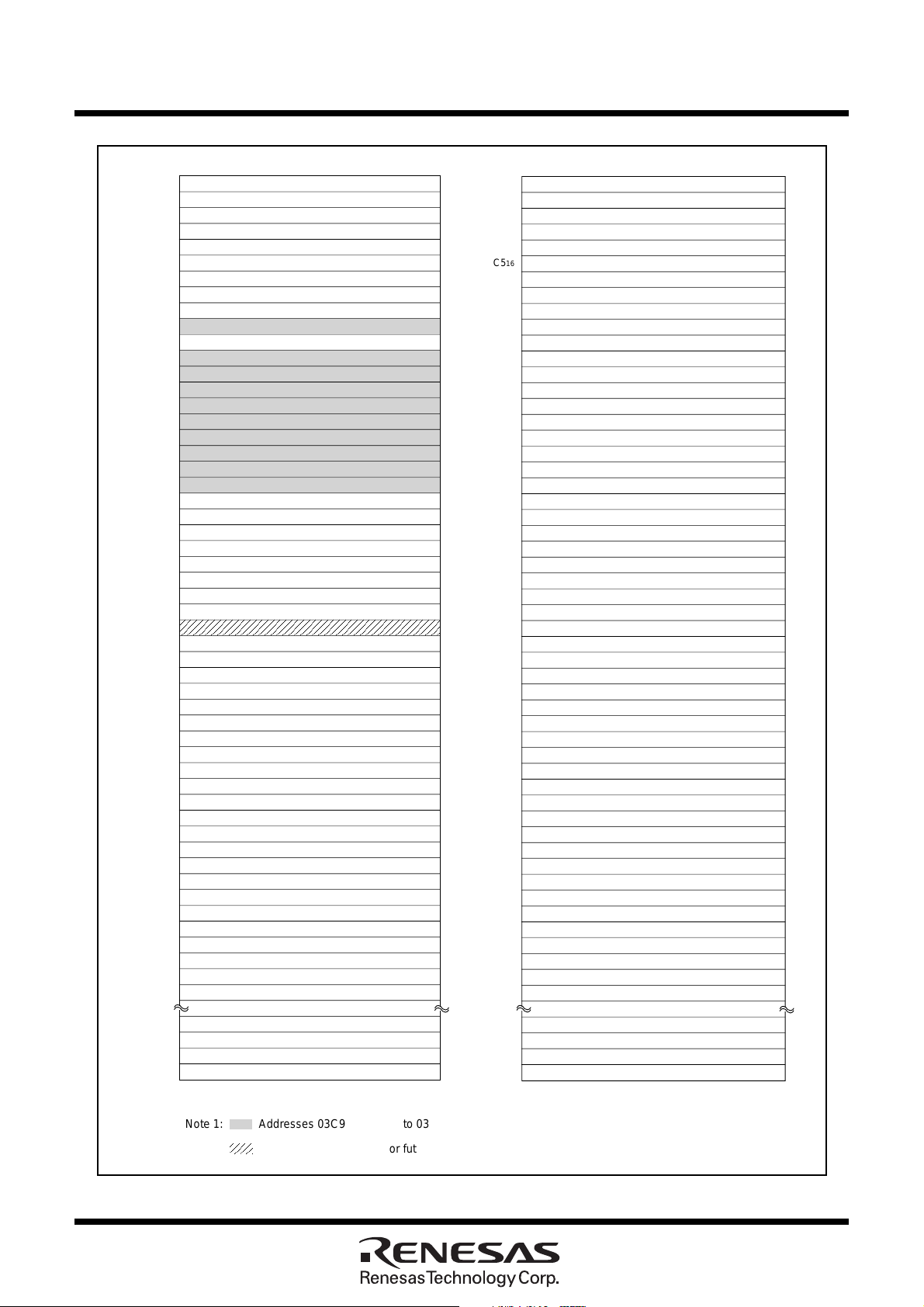
Under
development
SFR
Preliminary Specifications REV.D
Specifications in this manual are tentative and subject to change.
Mitsubishi Microcomputers
M16C/80 group
SINGLE-CHIP 16-BIT CMOS MICROCOMPUTER
<100-pin version>
03C0
16
03C1
03C2
03C3
03C4
03C5
03C6
03C7
03C8
03C9
03CA
03CB
03CC
03CD
03CE
03CF
03D0
03D1
03D2
03D3
03D4
03D5
03D6
03D7
03D8
03D9
03DA
03DB
03DC
03DD
03DE
03DF
03E0
03E1
03E2
03E3
03E4
03E5
03E6
03E7
03E8
03E9
03EA
03EB
03EC
03ED
03EE
03EF
03F0
03F1
03F2
03F3
Port P6 (P6)
16
Port P7 (P7)
16
Port P6 direction register (PD6)
16
Port P7 direction register (PD7)
16
Port P8 (P8)
16
Port P9 (P9)
16
Port P8 direction register (PD8)
16
Port P9 direction register (PD9)
16
Port P10 (P10)
16
16
Port P10 direction register (PD10)
16
16
16
16
16
16
16
16
16
16
16
16
16
16
16
16
Pull-up control register 2 (PUR2)
16
Pull-up control register 3 (PUR3)
16
16
16
16
16
Port P0 (P0)
16
Port P1 (P1)
16
Port P0 direction register (PD0)
16
Port P1 direction register (PD1)
16
Port P2 (P2)
16
Port P3 (P3)
16
Port P2 direction register (PD2)
16
Port P3 direction register (PD3)
16
Port P4 (P4)
16
Port P5 (P5)
16
Port P4 direction register (PD4)
16
Port P5 direction register (PD5)
16
16
16
16
16
Pull-up control register 0 (PUR0)
16
Pull-up control register 1 (PUR1)
16
16
<144-pin version>
03C0
16
03C1
03C2
03C3
03C4
03C5
03C6
03C7
03C8
03C9
03CA
03CB
03CC
03CD
03CE
03CF
03D0
03D1
03D2
03D3
03D4
03D5
03D6
03D7
03D8
03D9
03DA
03DB
03DC
03DD
03DE
03DF
03E0
03E1
03E2
03E3
03E4
03E5
03E6
03E7
03E8
03E9
03EA
03EB
03EC
03ED
03EE
03EF
03F0
03F1
03F2
03F3
Port P6 (P6)
16
Port P7 (P7)
16
Port P6 direction register (PD6)
16
Port P7 direction register (PD7)
16
Port P8 (P8)
16
Port P9 (P9)
16
Port P8 direction register (PD8)
16
Port P9 direction register (PD9)
16
Port P10 (P10)
16
Port P11 (P11)
16
Port P10 direction register (PD10)
16
Port P11 direction register (PD11)
16
Port P12 (P12)
16
Port P13 (P13)
16
Port P12 direction register (PD12)
16
Port P13 direction register (PD13)
16
Port P14 (P14)
16
Port P15 (P15)
16
Port P14 direction register (PD14)
16
Port P15 direction register (PD15)
16
16
16
16
16
16
16
Pull-up control register 2 (PUR2)
16
Pull-up control register 3 (PUR3)
16
Pull-up control register 4 (PUR4)
16
16
16
16
Port P0 (P0)
16
Port P1 (P1)
16
Port P0 direction register (PD0)
16
Port P1 direction register (PD1)
16
Port P2 (P2)
16
Port P3 (P3)
16
Port P2 direction register (PD2)
16
Port P3 direction register (PD3)
16
Port P4 (P4)
16
Port P5 (P5)
16
Port P4 direction register (PD4)
16
Port P5 direction register (PD5)
16
16
16
16
16
Pull-up control register 0 (PUR0)
16
Pull-up control register 1 (PUR1)
16
16
03FC
16
03FD
16
03FE
16
03FF
16
Port control register (PCR)
03FC
16
03FD
16
03FE
16
03FF
16
Port control register (PCR)
(The blank area is reserved and cannot be used by user.)
Note 1: Addresses 03C916, 03CB16 to 03D316 area is for future plan.
Must set "FF
Note 2: Address 03DC
16
" to address 03CB16, 03CE16, 03CF16, 03D216, 03D316 at initial setting.
16
area is for future plan. Must set "0016" to address 03DC16 at initial setting.
Figure 1.5.4. Location of peripheral unit control registers (4)
25

Under
development
Preliminary Specifications REV.D
Specifications in this manual are tentative and subject to change.
Software Reset
SINGLE-CHIP 16-BIT CMOS MICROCOMPUTER
Mitsubishi Microcomputers
M16C/80 group
Software Reset
Writing “1” to bit 3 of the processor mode register 0 (address 000416) applies a (software) reset to the
microcomputer. A software reset has the same effect as a hardware reset. The contents of internal RAM
are preserved.
Processor Mode
(1) Types of Processor Mode
One of three processor modes can be selected: single-chip mode, memory expansion mode, and microprocessor mode. The functions of some pins, the memory map, and the access space differ according to
the selected processor mode.
• Single-chip mode
In single-chip mode, only internal memory space (SFR, internal RAM, and internal ROM) can be
accessed. Ports P0 to P10 can be used as programmable I/O ports or as I/O ports for the internal
peripheral functions.
• Memory expansion mode
In memory expansion mode, external memory can be accessed in addition to the internal memory
space (SFR, internal RAM, and internal ROM).
In this mode, some of the pins function as the address bus, the data bus, and as control signals. The
number of pins assigned to these functions depends on the bus and register settings. (See “Bus
Settings” for details.)
• Microprocessor mode
In microprocessor mode, the SFR, internal RAM, and external memory space can be accessed. The
internal ROM area cannot be accessed.
In this mode, some of the pins function as the address bus, the data bus, and as control signals. The
number of pins assigned to these functions depends on the bus and register settings. (See “Bus
Settings” for details.)
(2) Setting Processor Modes
26
The processor mode is set using the CNVSS pin and the processor mode bits (bits 1 and 0 at address
000416). Do not set the processor mode bits to “102”.
Regardless of the level of the CNVSS pin, changing the processor mode bits selects the mode. Therefore,
never change the processor mode bits when changing the contents of other bits. Also do not attempt to
shift to or from the microprocessor mode within the program stored in the internal ROM area.
• Applying VSS to CNVSS pin
The microcomputer begins operation in single-chip mode after being reset. Memory expansion mode
is selected by writing “012” to the processor mode is selected bits.
• Applying VCC to CNVSS pin
The microcomputer starts to operate in microprocessor mode after being reset.
Figure 1.6.1 and 1.6.2 show the processor mode register 0 and 1.
Figure 1.6.3 shows the memory maps applicable for each processor modes.
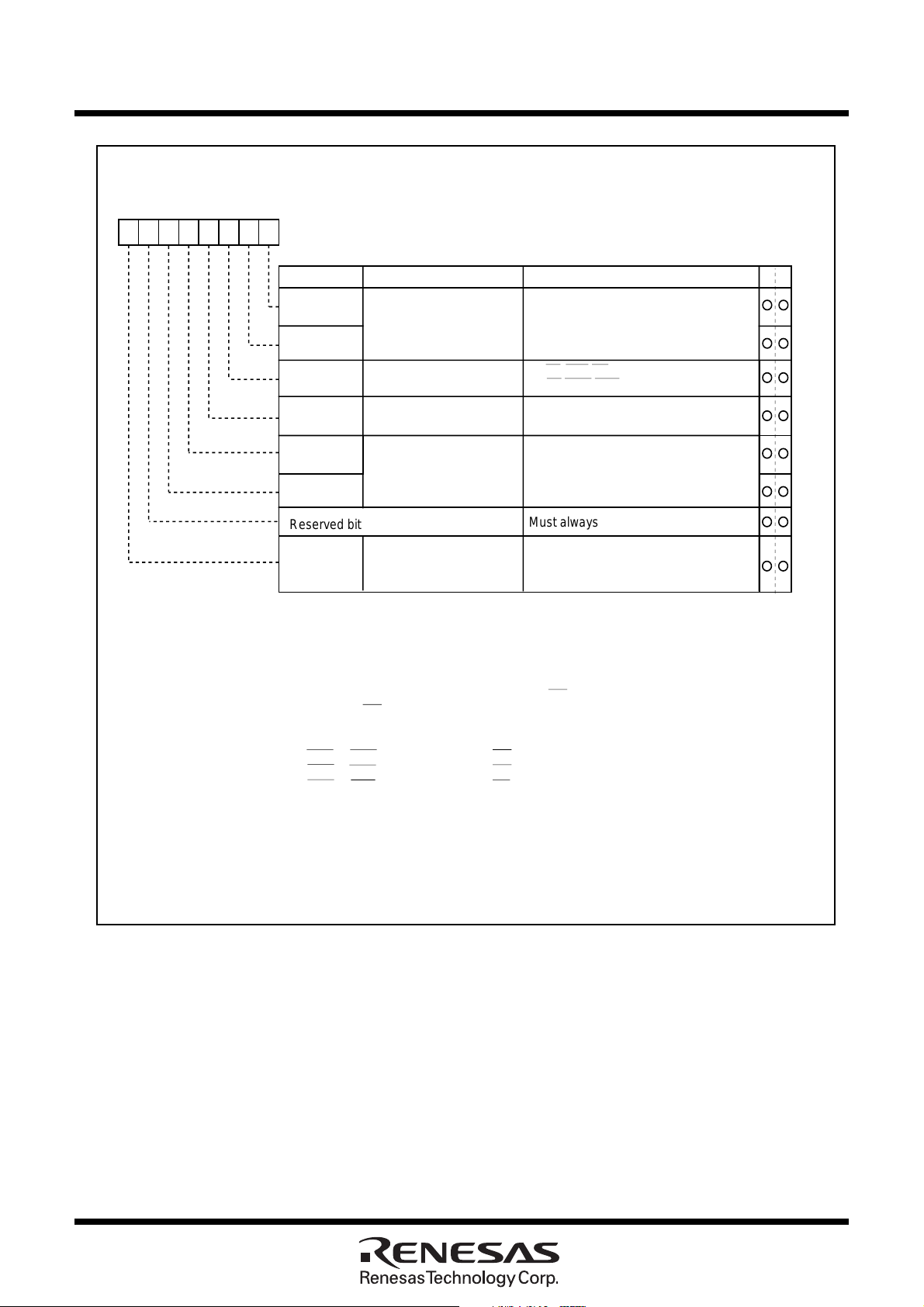
Under
development
Processor Mode
Specifications in this manual are tentative and subject to change.
Processor mode register 0 (Note 1)
b7 b6 b5 b4 b3 b2 b1 b0
0
Preliminary Specifications REV.D
SINGLE-CHIP 16-BIT CMOS MICROCOMPUTER
Symbol Address When reset
PM0 0004
16
80
16
(Note 2)
Mitsubishi Microcomputers
M16C/80 group
WR
PM00
PM01
PM02
PM03
PM04
PM05
Reserved bit
PM07
Bit name FunctionBit symbol
Processor mode bit
(Note 8)
R/W mode select bit
(Note 7)
Software reset bit
Multiplexed bus space
select bit (Note 3)
BCLK output disable bit
(Note 5)
b1 b0
0 0: Single-chip mode
0 1: Memory expansion mode
1 0: Inhibited
1 1: Microprocessor mode
0 : RD,BHE,WR
1 : RD,WRH,WRL
The device is reset when this bit is set to “1”.
The value of this bit is “0” when read.
b5 b4
0 0 : Multiplexed bus is not used
0 1 : Allocated to CS2 space
1 0 : Allocated to CS1 space
1 1 : Allocated to entire space (Note4)
Must always be set to “0”
0 : BCLK is output (Note 6)
1 : Function set by bit 0,1 of system
clock control register 0
Note 1: Set bit 1 of the protect register (address 000A
Note 2: If the V
CC
voltage is applied to the CNVSS, the value of this register when reset is 0316. (PM00 is set
16
) to “1” when writing new values to this register.
to “1” and PM07 is set to “0”.)
Note 3: Valid in microprocessor and memory expansion modes 1, 2 and 3. Do not use multiplex bus when
mode 0 is selected. Do not set to allocated to CS2 space when mode 2 is selected.
Note 4: After the reset has been released, the M16C/80 group MCU operates using the separate bus. As a
result, in microprocessor mode, you cannot select the full CS space multiplex bus.
When you select the full CS space multiplex bus in memory expansion mode, the address bus
operates with 64 Kbytes boundaries for each chip select.
Mode 0: Multiplexed bus cannot be used.
Mode 1: CS0 to CS2 when you select full CS space.
Mode 2: CS0 to CS1 when you select full CS space.
Mode 3: CS0 to CS3 when you select full CS space.
Note 5: No BCLK is output in single chip mode even when "0" is set in PM07. When stopping clock output in
microprocessor or memory expansion mode, make the following settings: PM07="1", bit 0 (CM00) and
bit 1 (CM01) of system clock control register 0 (address 0006
16
) = "0". "L" is now output from P53.
Note 6: When selecting BCLK, set bits 0 and 1 of system clock control register 0 (CM00, CM01) to "0".
Note 7: When using 16-bit bus width in DRAM controller, set this bit to "1".
Note 8: Do not set the processor mode bits and other bits simultaneously when setting the processor mode
bits to “01
2
” or “112”. Set the other bits first, and then change the processor mode bits.
Figure 1.6.1. Processor mode register 0
27
Under
development
Processor Mode
Specifications in this manual are tentative and subject to change.
Processor mode register 1 (Note 1) :Mask ROM version
b7 b6 b5 b4 b3 b2 b1 b0
Preliminary Specifications REV.D
Mitsubishi Microcomputers
M16C/80 group
SINGLE-CHIP 16-BIT CMOS MICROCOMPUTER
ROMless version (144-pin version)
Symbol Address When reset
0
PM1 0005
16
00
16
Bit name FunctionBit symbol
PM10
External memory area
mode bit (Note 3)
b1 b0
0 0 : Mode 0 (P4
0 1 : Mode 1 (P4
P4
PM11
1 0 : Mode 2 (P4
P4
1 1 : Mode 3 (Note 2)
(P4
4
to P47 : CS3 to CS0)
PM12
Internal memory wait bit 0 : No wait state
1 : Wait state inserted
Reserved bit
PM14
PM15
ALE pin select bit (Note 3)
Must always be set to “0”
b5 b4
0 0 : No ALE
0 1 : P5
3
1 0 : P5
1 1 : P5
/BCLK (Note 4)
6
/RAS
4
/HLDA
Nothing is assinged. When read, the content is indeterminate.
Note 1: Set bit 1 of the protect register (address 000A16) to “1” when writing new values to this register.
Note 2: When mode 3 is selected, DRAMC is not used.
Note 3: Valid in memory expansion mode or in microprocessor mode.
Note 4: When selecting P5
3
/BCLK, set bits 0 and 1 of system clock control register 0 (CM00, CM01) to "0".
Processor mode register 1 (Note 1) :Flash memory version
b7 b6 b5 b4 b3 b2 b1 b0
0
Symbol Address When reset
PM1 0005
16
00
16
4
to P47 : A20 to A23)
4
: A20,
5
to P47 : CS2 to CS0)
4
, P45 : A20, A21,
6
, P47 : CS1, CS0)
WR
PM10
External memory area
mode bit (Note 3)
PM11
PM12
Internal memory wait bit 0 : No wait state
Reserved bit
PM14
PM15
ALE pin select bit (Note 3)
Reserved bit
Note 1: Set bit 1 of the protect register (address 000A16) to “1” when writing new values to this register.
Note 2: When mode 3 is selected, DRAMC is not used.
Note 3: Valid in memory expansion mode or in microprocessor mode.
Note 4: When selecting P5
3
/BCLK, set bits 0 and 1 of system clock control register 0 (CM00, CM01) to "0".
Note 5: Rewrite this bit when the main clock is in division by 8 mode.
Figure 1.6.2. Processor mode register 1
Bit name FunctionBit symbol
b1 b0
0 0 : Mode 0 (P4
0 1 : Mode 1 (P4
P4
1 0 : Mode 2 (P4
P4
4
to P47 : A20 to A23)
4
: A20,
5
to P47 : CS2 to CS0)
4
, P45 : A20, A21,
6
, P47 : CS1, CS0)
WR
1 1 : Mode 3 (Note 2)
(P4
4
to P47 : CS3 to CS0)
1 : Wait state inserted
Must always be set to “0”
b5 b4
0 0 : No ALE
0 1 : P5
3
1 0 : P5
1 1 : P5
/BCLK (Note 4)
6
/RAS
4
/HLDA
Must always be set to “1” (Note 5)
28
Under
Single chip
mode
Memory expanded mode
Microprocessor mode
SFR area
Internal RAM area
Internal reserved area
Internal ROM area
No use
External area 0
CS2
2Mbytes
External area 1
CS0
2Mbytes
External area 3
No use
Internal ROM area
Internal reserved area
Internal ROM area
Internal reserved area
Internal ROM area
Internal reserved area
CS0
3Mbytes
External area 3
CS1
4Mbytes
(Note2)
External area 0
External area 3
No use
CS0
2Mbytes
External area 3
CS0
4Mbytes
External area 3
000000
16
000400
16
000800
16
200000
16
400000
16
C00000
16
E00000
16
F00000
16
FFFFFF
16
Each CS0 to CS3 can set 0 to 3 WAIT.
Mode 0
Mode 1 Mode 2 Mode 0
Mode 1
Mode 2
SFR area
Internal RAM area
Internal reserved area
SFR area
Internal RAM area
Internal reserved area
SFR area
Internal RAM area
Internal reserved area
SFR area
Internal RAM area
Internal reserved area
SFR area
Internal RAM area
Internal reserved area
SFR area
Internal RAM area
Mode 3
Internal reserved area
SFR area
Internal RAM area
Internal ROM area
Internal reserved area
CS1, 1Mbytes
External area 0
Mode 3
Internal reserved area
SFR area
Internal RAM area
No use
CS2, 1Mbytes
External area 1
No use
Connect with
DRAM
0, 0.5 to 8MB
(When not
connect with
DRAM, use as
external area.)
Connect with
DRAM
0, 0.5 to 8MB
(When open area
is under 8MB,
cannot use the
rest of this area.)
Connect with
DRAM
0, 0.5 to 8MB
(When open area
is under 8MB,
cannot use the
rest of this area.)
Connect with
DRAM
0, 0.5 to 8MB
(When open area
is under 8MB,
cannot use the
rest of this area.)
No use
(Cannot use as
DRAM area or
external area.)
Connect with
DRAM
0, 0.5 to 8MB
(When not
connect with
DRAM, use as
external area.)
Connect with
DRAM
0, 0.5 to 8MB
(When open area
is under 8MB,
cannot use the
rest of this area.)
No use
(Cannot use as
DRAM area or
external area.)
No use
No use
No use
CS1
2Mbytes
(Note1)
External area 0
No use
Note 1: 200000
16
–008000
16
=2016 Kbytes. 32 K less than 2 MB.
Note 2: 400000
16
–008000
16
=4064 Kbytes. 32 K less than 4 MB.
External area 1
External area 0
CS2
2Mbytes
External area 1
CS1
4Mbytes
(Note2)
External area 0
CS1, 1Mbytes
External area 0
CS2, 1Mbytes
External area 1
CS1
2Mbytes
(Note1)
External area 0
External area 1
(External area 2) (External area 2) (External area 2)
(External area 2) (External area 2) (External area 2)
External area 3
CS3, 1Mbytes
External area 2
CS0, 1Mbytes
External area 3
CS3, 1Mbytes
External area 2
CS0, 1Mbytes
External area 3
Preliminary Specifications REV.D
development
Processor Mode
Processor Mode
Specifications in this manual are tentative and subject to change.
Mitsubishi Microcomputers
M16C/80 group
SINGLE-CHIP 16-BIT CMOS MICROCOMPUTER
Figure 1.6.3. Memory maps in each processor mode
29

Under
development
Bus Settings
Preliminary Specifications REV.D
Specifications in this manual are tentative and subject to change.
SINGLE-CHIP 16-BIT CMOS MICROCOMPUTER
Mitsubishi Microcomputers
M16C/80 group
Bus Settings
The BYTE pin, bit 0 to 3 of the external data bus width control register (address 000B16), bits 4 and 5 of the
processor mode register 0 (address 000416) and bit 0 and 1 of the processor mode register 1 (address
000516) are used to change the bus settings.
Table 1.7.1 shows the factors used to change the bus settings, figure 1.7.1 shows external data bus width
control register and table 1.7.2 shows external area 0 to 3 and external area mode.
Table 1.7.1. Factors for switching bus settings
Bus setting Switching factor
Switching external address bus width External data bus width control register
Switching external data bus width BYTE pin (external area 3 only)
Switching between separate and multiplex bus Bits 4 and 5 of processor mode register 0
(1) Selecting external address bus width
You can select the width of the address bus output externally from the 16 Mbytes address space, the
number of chip select signals, and the address area of the chip select signals. (Note, however, that when
you select “Full CS space multiplex bus”, addresses A0 to A15 are output.) The combination of bits 0 and
1 of the processor mode register 1 allow you to set the external area mode.
When using DRAM controller, the DRAM area is output by multiplexing of the time splitting of the row and
column addresses.
____
(2) Selecting external data bus width
You can select 8-bit or 16-bit for the width of the external data bus for external areas 0, 1, 2, and 3. When
the data bus width bit of the external data bus width control register is “0”, the data bus width is 8 bits;
when “1”, it is 16 bits. The width can be set for each of the external areas. The default bus width for
external area 3 is 16 bits when the BYTE pin is “L” after a reset, or 8 bits when the BYTE pin is “H” after
a reset. The bus width selection is valid only for the external bus (the internal bus width is always 16 bits).
During operation, fix the level of the BYTE pin to “H” or “L”.
(3) Selecting separate/multiplex bus
The bus format can be set to multiplex or separate bus using bits 4 and 5 of the processor mode register 0.
• Separate bus
In this bus configuration, input and output is performed on separate data and address buses. The data
bus width can be set to 8 bits or 16 bits using the external data bus width control register. For all
programmable external areas, P0 is the data bus when the external data bus is set to 8 bits, and P1 is
a programmable IO port. When the external data bus width is set to 16 bits for any of the external
areas, P0 and P1 (although P1 is undefined for any 8-bit bus areas) are the data bus.
When accessing memory using the separate bus configuration, you can select a software wait using
the wait control register.
• Multiplex bus
In this bus configuration, data and addresses are input and output on a time-sharing basis. For areas
for which 8-bit has been selected using the external data bus width control register, the 8 bits D0 to D7
are multiplexed with the 8 bits A0 to A7. For areas for which 16-bit has been selected using the external
data bus width control register, the 16 bits D0 to D15 are multiplexed with the 16 bits A0 to A15. When
accessing memory using the multiplex bus configuration, two waits are inserted regardless of whether
you select “No wait” or “1 wait’ in the appropriate bit of the wait control register.
30

Under
development
Specifications in this manual are tentative and subject to change.
Bus Settings
Preliminary Specifications REV.D
Mitsubishi Microcomputers
M16C/80 group
SINGLE-CHIP 16-BIT CMOS MICROCOMPUTER
The default after a reset is the separate bus configuration, and the full CS space multiplex bus configu-
____
____
ration cannot be selected in microprocessor mode. If you select “Full CS space multiplex bus”, the 16
bits from A0 to A15 are output for the address
External data bus width control register
b7 b6 b5 b4 b3 b2 b1 b0
Symbol Address When reset
DS 000B
16
XXXXX000
2
Bit name FunctionBit symbol
DS0
DS1
DS2
DS3
Nothing is assigned.
When write, set "0". When read, their contents are indeterminate.
Note: The value after a reset is determined by the input via the BYTE pin.
External area 0 data bus
width bit
External area 1 data bus
width bit
External area 2 data bus
width bit
External area 3 data bus
width bit (Note)
0 : 8 bits data bus width
1 : 16 bits data bus width
0 : 8 bits data bus width
1 : 16 bits data bus width
0 : 8 bits data bus width
1 : 16 bits data bus width
0 : 8 bits data bus width
1 : 16 bits data bus width
WR
Figure 1.7.1. External data bus width control register
Table 1.7.2. External area 0 to 3 and external area mode
External area mode
Memory expansion mode
Microprocessor mode
area 0
External
Memory expansion mode
Microprocessor mode
area 1
External
Memory expansion mode
Microprocessor mode
area 2
External
Memory expansion mode
area 3
External
Microprocessor mode
(Note 2)
,
,
,
Mode 0 Mode 1 Mode 2 Mode 3
00800016 to
1FFFFF
16
20000016 to
3FFFFF
16
40000016 to
BFFFFF
16
(Note 1)
C0000016 to
EFFFFF
16
C0000016 to
FFFFFF
16
<CS1 area>
008000
1FFFFF
16
to
16
<CS2 area>
200000
3FFFFF
16
to
16
<DRAMC area>
400000
BFFFFF
16
to
16
<CS0 area>
C00000
EFFFFF
16
to
16
<CS0 area>
E00000
FFFFFF
16
to
16
<CS1 area>
008000
1FFFFF
16
to
16
No area is
selected.
<DRAMC area>
400000
BFFFFF
16
to
16
<CS0 area>
C00000
EFFFFF
16
to
16
<CS0 area>
C00000
FFFFFF
16
to
16
<CS1 area>
100000
1FFFFF
<CS2 area>
200000
2FFFFF
<CS3 area>
C00000
CFFFFF
<CS0 area>
E00000
EFFFFF
<CS0 area>
F00000
FFFFFF
16
16
16
16
16
to
16
to
16
to
16
to
16
to
16
Note 1: DRAMC area when using DRAMC.
Note 2:Set the external area mode (modes 0, 1, 2, and 3) using bits 0 and 1 of the processor mode register
1 (address 000516).
31

Under
development
Bus Settings
Specifications in this manual are tentative and subject to change.
Table 1.7.3. Each processor mode and port function
Preliminary Specifications REV.D
Processor
mode
Single-chip
mode
Memory expansion mode/microprocessor modes
Mitsubishi Microcomputers
M16C/80 group
SINGLE-CHIP 16-BIT CMOS MICROCOMPUTER
Memory
expansion mode
Multiplexed
bus space
select bit
Data bus width
BYTE pin level
“01”, “10”
CS1 or CS2 : multiplexed
bus, and the other :
separate bus
All external
area is 8 bits
Some external
area is 16 bits
Separate bus
All external
area is 8 bits
“00”
Some external
area is 16 bits
area is 8 bits
“11” (Note 1)
All space multiplexed
bus
All external
Some external
area is 16 bits
P00 to P07I/O port Data bus Data bus Data bus Data bus I/O port I/O port
P10 to P17I/O port I/O port Data bus I/O port Data bus I/O port I/O port
P2
0
to P2
7
P30 to P3
P4
0
to P4
P4
4
to P4
I/O port
7
I/O port
3
I/O port Address bus Address bus Address bus Address bus I/O port I/O port
6
I/O port CS (chip select) or address bus (A20 to A22)
Address bus Address bus
/data bus /data bus
(Note 2)
Address bus Address bus
(Note 2)
/data bus
(Note 2)
Address bus Address bus Address bus Address bus
/data bus /data bus
Address bus Address bus Address bus Address bus
/data bus
(For details, refer to “Bus control”) (Note 5)
P4
7
I/O port
CS (chip select) or address bus (A23)
(For details, refer to “Bus control”) (Note 5)
P5
0
to P5
3
I/O port
Outputs RD, WRL, WRH and BCLK, or RD, BHE, WR and BCLK
(For details, refer to “Bus control”) (Note 3,4)
P5
P5
P5
P5
4
5
6
7
I/O port HLDA(Note 3) HLDA(Note 3) HLDA(Note 3) HLDA(Note 3) HLDA(Note 3) HLDA(Note 3)
I/O port HOLD HOLD HOLD HOLD HOLD HOLD
I/O port RAS (Note 3) RAS (Note 3) RAS (Note 3) RAS (Note 3) RAS (Note 3) RAS (Note 3)
I/O port RDY RDY RDY RDY RDY RDY
Note 1:The default after a reset is the separate bus configuration, and "Full CS space multiplex bus" cannot be selected in
microprocessor mode. When you select "Full CS space multiplex bus" in extended memory mode, the address bus
operates with 64 Kbytes boundaries for each chip select.
Note 2: Address bus in separate bus configuration.
Note 3: The ALE output pin is selected using bits 4 and 5 of the processor mode register 1.
Note 4: When you have selected use of the DRAM controller and you access the DRAM area, these are CASL, CASH, DW, and
BCLK outputs.
Note 5: The CS signal and address bus selection are set by the external area mode.
32

Under
Preliminary Specifications REV.D
development
Bus Control
Specifications in this manual are tentative and subject to change.
SINGLE-CHIP 16-BIT CMOS MICROCOMPUTER
Mitsubishi Microcomputers
M16C/80 group
Bus Control
The following explains the signals required for accessing external devices and software waits. The signals
required for accessing the external devices are valid when the processor mode is set to memory expansion
mode and microprocessor mode.
(1) Address bus/data bus
There are 24 pins, A0 to A22 and A23 for the address bus for accessing the 16 Mbytes address space. A23
is an inverted output of the MSB of the address.
The data bus consists of pins for data IO. The external data bus control register (address 000B16) selects
the 8-bit data bus, D0 to D7 for each external area, or the 16-bit data bus, D0 to D15. After a reset, there is
by default an 8-bit data bus for the external area 3 when the BYTE pin is “H”, or a 16-bit data bus when the
BYTE pin is “L”.
When shifting from single-chip mode to extended memory mode, the value on the address bus is undefined until an external area is accessed.
When accessing a DRAM area with DRAM control in use, a multiplexed signal consisting of row address
and column address is output to A8 to A20.
(2) Chip select signals
The chip select signals share A0 to A22 and A23. You can use bits 0 and 1 of the processor mode register
1 (address 000516) to set the external area mode, then select the chip select area and number of address
outputs.
In microprocessor mode, external area mode 0 is selected after a reset. The external area can be split
into a maximum of four using the chip select signals. Table 1.7.4 shows the external areas specified by
the chip select signals.
____ ____
____
Table 1.7.4. External areas specified by the chip select signals
Memory space
expansion
mode
Mode 0
Mode 1
Mode 2
Specified address range
Mode 3
Processor mode
Memory expansion mode
Microprocessor mode
Memory expansion mode
Microprocessor mode
Memory expansion mode
Microprocessor mode
CS0
(A23)
C0000016 to
DFFFFF
(2 Mbytes)
E0000016 to
FFFFFF
(2 Mbytes)
C00000
EFFFFF
(3 Mbytes)
C00000
FFFFFF
(4 Mbytes)
E00000
EFFFFF
(1 Mbytes)
F0000016 to
FFFFFF
(1 Mbytes)
16
16
16
to
16
16
to
16
16
to
16
16
CS1 CS2 CS3
(A22) (A21) (A20)
00800016 to
1FFFFF
(2016 Kbytes)
008000
3FFFFF
(4064 Kbytes)
100000
1FFFFF
(1 Mbytes)
Chip select signal
200000
16
16
to
16
16
to
16
3FFFFF
(2 Mbytes)
(A21) (A20)
200000
2FFFFF
(1 Mbytes)
16
to
16
16
to
16
(A20)
16
C00000
CFFFFF
(1 Mbytes)
to
16
33

Under
Preliminary Specifications REV.D
development
Bus Control
Specifications in this manual are tentative and subject to change.
SINGLE-CHIP 16-BIT CMOS MICROCOMPUTER
Mitsubishi Microcomputers
M16C/80 group
The chip select signal turns “L” (active) in synchronize with the address bus. However, its turning “H”
depends on the area accessed in the next cycle. Figure 1.7.2 shows the output examples of the address
bus and chip select signals.
(Example 1) After accessing the external area, the address bus and chip
(Example 3) After accessing the external area, only the address bus is
select signal both are changed in the next cycle.
The following example shows the other chip select signal accessing
area (j) in the cycle after having accessed external area (i). In this
case, the address bus and chip select signal both change between the
two cycles.
Access to
Access to
external
external
area (j)
area (i)
Data bus
Address bus
Chip select
(CSi)
Chip select
(CSj)
changed in the next cycle. (The chip select signal does not
change.)
The following example shows the same chip select signal
accessing area (i) in the cycle after having accessed
external area (i). In this case, the address bus changes
between the two cycles, but the chip select signal does not.
Address
Access to
external
area (i)
Data
Access to
external
area (i)
Data
(Example 2) After accessing the external area, only the chip select signal
(Example 4) After accessing the external area, the address bus and chip
is changed in the next cycle. (The address bus does not
change.)
The following example shows the CPU accesses the internal
ROM/RAM area in the cycle after having accessed external
area. In this case, the chip select signal changes between the
two cycles but the address bus does not.
Data bus
Address bus
Chip select
select signal both are not changed in the next cycle.
The following example shows CPU does not access any
area in the cycle after having accessed external area (no
instruction pre-fetch is occurred). In this case, the address
bus and the chip select signal do not change between the
two cycles.
Data
Address
Access to
external
area
No access
Data bus
Address bus
Chip select
(CSi)
Address
Note: These examples show the address bus and chip select signal for two consecutive cycles.
By combining these examples, chip select signal can be extended beyond two cycles.
Data
Data
Data bus
Address bus
Chip select
Data
Address
Figure 1.7.2. Example of address bus and chip select signal outputs (Separate bus)
34

Under
Preliminary Specifications REV.D
development
Bus Control
Specifications in this manual are tentative and subject to change.
SINGLE-CHIP 16-BIT CMOS MICROCOMPUTER
Mitsubishi Microcomputers
M16C/80 group
(3) Read/write signals
With a 16-bit data bus, bit 2 of the processor mode register 0 (address 000416) select the combinations of
_____ ________ ______ _____ ________ _________
RD, BHE, and WR signals or RD, WRL, and WRH signals. With a 8-bit full space data bus, use the
combination of RD, WR, and BHE signals as read/write signals. (Set "0" to bit 2 of the processor mode
register 0 (address 000416).) When using both 8-bit and 16-bit data bus widths and you access an 8-bit
data bus area, the RD, WR and BHE signals combination is selected regardless of the value of bit 2 of the
processor mode register 0 (address 000416).
Tables 1.7.5 and 1.7.6 show the operation of these signals.
After a reset has been cancelled, the combination of RD, WR, and BHE signals is automatically selected.
When switching to the RD, WRL, and WRH combination, do not write to external memory until bit 2 of the
processor mode register 0 (address 000416) has been set (Note).
Note 1: Before attempting to change the contents of the processor mode register 0, set bit 1 of the protect
register (address 000A16) to “1”.
Note 2: When using 16-bit data bus width for DRAM controller, select RD, WRL, and WRH signals.
_____ ______ ________
_____ ______ ________
_____ ______ ________
_____ _________ _________
_____ ________ _________
Table 1.7.5. Operation of RD, WRL, and WRH signals
_____ ________ _________
Data bus width
16-bit
8-bit
______
L
H
H
H
H
L
H
L
H
L
L (Note)
H (Note)
WRHWRLRD
H
H
L
L
Not used
Not used
Note: It becomes WR signal.
Table 1.7.6. Operation of RD, WR, and BHE signals
_____ ______ ________
Data bus width A0
16-bit
8-bit
RD
HLL
LHL
HLH
LHH
HLLL
LHLL
HL H / L
LH H / L
BHEWR
Not used
Not used
Status of external data bus
Read data
Write 1 byte of data to even address
Write 1 byte of data to odd address
Write data to both even and odd addresses
Write 1 byte of data
Read 1 byte of data
Status of external data bus
H
H
L
L
Write 1 byte of data to odd address
Read 1 byte of data from odd address
Write 1 byte of data to even address
Read 1 byte of data from even address
Write data to both even and odd addresses
Read data from both even and odd addresses
Write 1 byte of data
Read 1 byte of data
35

Under
Preliminary Specifications REV.D
development
Bus Control
Specifications in this manual are tentative and subject to change.
SINGLE-CHIP 16-BIT CMOS MICROCOMPUTER
Mitsubishi Microcomputers
M16C/80 group
(4) ALE signal
The ALE signal latches the address when accessing the multiplex bus space. Latch the address when the
ALE signal falls. The ALE output pin is selected using bits 4 and 5 of the processor mode register 1
(address 000516).
The ALE signal is occurred regardless of internal area and external area.
When BYTE pin = “H”
ALE
D
0/A0
to D7/A
A8 to A
15
A16 to A
A20 to A22, A
19
ALE
7
23
Address Data (Note 1)
Address
Address (Note 2)
Address or CS
Note 1: Floating when reading.
Note 2: When full space multiplexed bus is selected, these are I/O ports.
D
A16 to A
A20 to A22, A
When BYTE pin = “L”
0/A0
to D15/A
19
23
15
Address Data (Note 1)
Address (Note 2)
Address or CS
Figure 1.7.3. ALE signal and address/data bus
(5) Ready signal
The ready signal facilitates access of external devices that require a long time for access. As shown in
Figure 1.7.2, inputting “L” to the RDY pin at the falling edge of BCLK causes the microcomputer to enter
the ready state. Inputting “H” to the RDY pin at the falling edge of BCLK cancels the ready state. Table
1.7.7 shows the microcomputer status in the ready state. Figure 1.7.4 shows the example of the RD
signal being extended using the RDY signal.
Ready is valid when accessing the external area during the bus cycle in which the software wait is applied. When no software wait is operating, the RDY signal is ignored, but even in this case, unused pins
must be pulled up.
________
________
________
________
_____
Table 1.7.7. Microcomputer status in ready state (Note)
Item Status
Oscillation On
_____ _____ _____
RD/WR signal, address bus, data bus, CS Maintain status when ready signal received
__________
ALE signal, HLDA, programmable I/O ports
Internal peripheral circuits On
Note: The ready signal cannot be received immediately prior to a software wait.
36

Under
development
Bus Control
Separate bus (2 wait)
BCLK
RD
CS
(i=0 to 3)
RDY
Preliminary Specifications REV.D
Specifications in this manual are tentative and subject to change.
1st cycle 2nd cycle 3rd cycle 4th cycle
(Note)
i
tsu(RDY - BCLK)
Mitsubishi Microcomputers
M16C/80 group
SINGLE-CHIP 16-BIT CMOS MICROCOMPUTER
Multiplexed bus (2 wait)
1st cycle 2nd cycle 3rd cycle 4th cycle
BCLK
RD
(Note)
CS
i
(i=0 to 3)
RDY
: Wait using RDY signal
: Wait using software
RDY received timing
tsu(RDY - BCLK)
RDY received timing
RDY signal received timing for i wait(s): i + 1 cycles
(i = 1 to 3)
Note: Chip select may get longer by a state of CPU such as an instruction queue buffer.
_____ ________
Figure 1.7.4. Example of RD signal extended by RDY signal
37

Under
Preliminary Specifications REV.D
development
Bus Control
Specifications in this manual are tentative and subject to change.
SINGLE-CHIP 16-BIT CMOS MICROCOMPUTER
Mitsubishi Microcomputers
M16C/80 group
(6) Hold signal
The hold signal is used to transfer the bus privileges from the CPU to the external circuits. Inputting “L” to
__________
the HOLD pin places the microcomputer in the hold state at the end of the current bus access. This status
__________ __________
is maintained and “L” is output from the HLDA pin as long as “L” is input to the HOLD pin. Table 1.7.8
shows the microcomputer status in the hold state. The bus is used in the following descending order of
__________
priority: HOLD, DMAC, CPU.
__________
HOLD > DMAC > CPU
Figure 1.7.5. Example of RD signal extended by RDY signal
_____ ________
Table 1.7.8. Microcomputer status in hold state
Item Status
Oscillation ON
_____ _____ _____ _______
RD/WR signal, address bus, data bus, CS, BHE Floating
Programmable I/O ports P0, P1, P2, P3, P4, P5 Maintains status when hold signal is received
P6, P7, P8, P9, P10
__________
P11, P12, P13, P14, P15 (Note)
HLDA Output “L”
Internal peripheral circuits ON (but watchdog timer stops)
ALE signal Undefined
Note: Ports P11 to P15 exist in 144-pin version.
(7) External bus status when accessing to internal area
Table 1.7.9 shows external bus status when accessing to internal area
Table 1.7.9. External bus status when accessing to internal area
Item SFR accessing status Internal ROM/RAM accessing status
Address bus Remain address of external area accessed immediately before
Data bus When read Floating
When write Floating
_____ ______ ________ _________
RD, WR, WRL, WRH Output "H"
________
BHE Remain external area status accessed immediately before
____
CS Output "H"
ALE ALE output
(8) BCLK output
BCLK output can be selected by bit 7 of the processor mode register 0 (address 000416 :PM07) and bit 1
and bit 0 of the system clock select register 0 (address 000616 :CM01, CM00). Setting PM07 to “0” and
CM01 and CM00 to “00” outputs the BCLK signal from P53. However, in single chip mode, BCLK signal
is not output. When setting PM07 to “1”, the function is as set by CM01 and CM00.
38

Under
Preliminary Specifications REV.D
development
Bus Control
Specifications in this manual are tentative and subject to change.
SINGLE-CHIP 16-BIT CMOS MICROCOMPUTER
_______ __________ __________ _____
Mitsubishi Microcomputers
M16C/80 group
(9) DRAM controller signals (RAS, CASL, CASH, and DW)
Bits 1, 2, and 3 of the DRAM control register (address 000416) select the DRAM space and enable the
DRAM controller. The DRAM controller signals are then output when the DRAM area is accessed. Table
1.7.10 shows the operation of the respective signals.
Table 1.7.10. Operation of RAS, CASL, CASH, and DW signals
_______ __________ __________ _____
Data bus width DW
16-bit
8-bit
RAS
LLL
LLL
LHH
LLL
LLHL
LHLL
LL H
LL L
CASHCASL
H
H
H
L
Not used
Not used
Read data from both even and odd addresses
Read 1 byte of data from even address
Read 1 byte of data from odd address
Write data to both even and odd addresses
Write 1 byte of data to even address
Write 1 byte of data to odd address
Read 1 byte of data
Write 1 byte of data
Status of external data bus
(10) Software wait
A software wait can be inserted by setting the wait control register (address 000816). Figure 1.7.6 shows
wait control register
You can use the external area I wait bits (where I = 0 to 3) of the wait control register to specify from “No
wait” to “3 waits” for the external memory area. When you select “No wait”, the read cycle is executed in
the BCLK1 cycle. The write cycle is executed in the BCLK2 cycle (which has 1 wait). When accessing
external memory using the multiplex bus, access has two waits regardless of whether you specify “No
wait” or “1 wait” in the appropriate external area i wait bits in the wait control register.
Software waits in the internal memory (internal RAM and internal ROM) can be set using the internal
memory wait bits of the processor mode register 1 (address 000516). Setting the internal memory wait bit
= “0” sets “No wait”. Setting the internal memory wait bit = “1” specifies a wait.
The SFR area is not affected by the setting of the internal memory wait bit and is always accessed in the
BCLK2 cycle.
Table 1.7.11 shows the software waits and bus cycles. Figures 1.7.7 and 1.7.8 show example bus timings
when using software waits.
39

Under
development
Bus Control
Wait control register
b7 b6 b5 b4 b3 b2 b1 b0
Preliminary Specifications REV.D
Specifications in this manual are tentative and subject to change.
Symbol Address When reset
WCR 0008
16
Mitsubishi Microcomputers
M16C/80 group
SINGLE-CHIP 16-BIT CMOS MICROCOMPUTER
FF
16
WCR0
WCR1
WCR2
WCR
WCR4
WCR5
WCR6
WCR7
Note 1: When using the multiplex bus configuration, there are two waits regardless of whether
you have specified "No wait" or "1 wait". However, you can specify "2 wait" or "3 wait".
Note 2: When using the separate bus configuration, the read bus cycle is executed in the
BCLK1 cycle, and the write cycle is executed in the BCLK2 cycle (with 1 wait).
Figure 1.7.6. Wait control register
Bit name FunctionBit symbol
External area 0 wait bit
External area 1 wait bit
External area 2 wait bit
External area 3 wait bit
WR
b1 b0
0 0: Without wait
0 1: With 1 wait
1 0: With 2 wait
1 1: With 3 wait
b3 b2
0 0: Without wait
0 1: With 1 wait
1 0: With 2 wait
1 1: With 3 wait
b5 b4
0 0: Without wait
0 1: With 1 wait
1 0: With 2 wait
1 1: With 3 wait
b7 b6
0 0: Without wait
0 1: With 1 wait
1 0: With 2 wait
1 1: With 3 wait
Table 1.7.11. Software waits and bus cycles
Area Bus status
Internal
memory wait bit
SFR
Internal
ROM/RAM
0 1 BCLK cycle
1 2 BCLK cycles
Separate bus
External
memory
area
Multiplex bus
External memory
area i wait bit
00
2
01
2
10
2
11
2
00
2
01
2
10
2
11
2
Bus cycle
2 BCLK cycles
Read :1 BCLK cycle
Write : 2 BCLK cycles
2 BCLK cycles
3 BCLK cycles
4 BCLK cycles
3 BCLK cycle
3 BCLK cycles
3 BCLK cycles
4 BCLK cycles
40

Under
Preliminary Specifications REV.D
development
Bus Control
Specifications in this manual are tentative and subject to change.
Mitsubishi Microcomputers
M16C/80 group
SINGLE-CHIP 16-BIT CMOS MICROCOMPUTER
< Separate bus (no wait) >
BCLK
Write signal
Read signal
Data bus
Address bus (Note 2)
Chip select (Note 2,3)
< Separate bus (with wait) >
BCLK
Write signal
Read signal
Bus cycle (Note)
Output
Address
Bus cycle (Note)
Bus cycle (Note)
Input
Address
Bus cycle (Note)
Data bus
Address bus (Note 2)
Chip select (Note 2,3)
< Separate bus with 2 wait >
BCLK
Write signal
Read signal
Data bus
Address bus (Note 2)
Chip select (Note 2,3)
Note 1: This timing example shows bus cycle length. Read cycle and write cycle may be continued after this
bus cycle.
Note 2: Address bus and chip select may get longer by a state of CPU such as an instruction queue buffer.
Note 3: When accessing same external area (same CS area) continuously, chip select may output
continuously.
Bus cycle (Note 1)
Data output
Address
Output
Address
Address
Bus cycle (Note 1)
Address
Input
Input
Figure 1.7.7. Typical bus timings using software wait
41

Under
Preliminary Specifications REV.D
development
Bus Control
Specifications in this manual are tentative and subject to change.
Mitsubishi Microcomputers
M16C/80 group
SINGLE-CHIP 16-BIT CMOS MICROCOMPUTER
< Separate bus (with 3 wait) >
BCLK
Write signal
Read signal
Data bus
Address
(Note 2)
Chip select
(Note 2,3)
< Multiplexed bus (with 2 wait) >
BCLK
Write signal
Read signal
ALE
Bus cycle (Note)
Data output
Address
Bus cycle (Note)
Bus cycle (Note)
Input
Address
Bus cycle (Note)
Address
Address bus/Data bus
(Note 2)
Chip select
(Note 2,3)
< Multiplexed bus (with 3 wait) >
BCLK
Write signal
Read signal
Address
Address bus
/Data bus
(Note 2)
ALE
Chip select
(Note 2,3)
Address Address
Address
Address
Bus cycle (Note)
Address
Data output
Data output
Address
Bus cycle (Note)
Address
Input
Address
Input
Note 1: This timing example shows bus cycle length. Read cycle and write cycle may be continued after this
bus cycle.
Note 2: Address bus and chip select may get longer by a state of CPU such as an instruction queue buffer.
Note 3: When accessing same external area (same CS area) continuously, chip select may output
continuously.
Figure 1.7.8. Typical bus timings using software wait
42

Under
development
Specifications in this manual are tentative and subject to change.
Clock Generating Circuit
Preliminary Specifications REV.D
SINGLE-CHIP 16-BIT CMOS MICROCOMPUTER
Mitsubishi Microcomputers
M16C/80 group
Clock Generating Circuit
The clock generating circuit contains two oscillator circuits that supply the operating clock sources to the
CPU and internal peripheral units.
Table 1.8.1. Main clock and sub clock generating circuits
Main clock generating circuit Sub clock generating circuit
Use of clock • CPU’s operating clock source • CPU’s operating clock source
• Internal peripheral units’ • Timer A/B’s count clock
operating clock source source
Usable oscillator Ceramic or crystal oscillator Crystal oscillator
Pins to connect oscillator XIN, XOUT XCIN, XCOUT
Oscillation stop/restart function Available Available
Oscillator status immediately after reset
Other Externally derived clock can be input
Oscillating Stopped
Example of oscillator circuit
Figure 1.8.1 shows some examples of the main clock circuit, one using an oscillator connected to the
circuit, and the other one using an externally derived clock for input. Figure 1.8.2 shows some examples
of sub clock circuits, one using an oscillator connected to the circuit, and the other one using an externally
derived clock for input. Circuit constants in Figures 1.8.1 and 1.8.2 vary with each oscillator used. Use
the values recommended by the manufacturer of your oscillator.
Microcomputer
(Built-in feedback resistance)
X
IN
C
IN
Note: Insert a damping resistance if required. The resistance will vary depending on the oscillator and the oscillation
drive capacity setting. Use the value recommended by the maker of the oscillator.
When the oscillation drive capacity is set to low, check that oscillation is stable.
Insert a feedback resistance between X
X
OUT
(Note)
R
d
C
OUT
Figure 1.8.1. Examples of main clock
IN
and X
OUT
when an oscillation manufacture required.
Microcomputer
(Built-in feedback resistance)
X
IN
Externally derived clock
Vcc
Vss
X
Open
OUT
Microcomputer
(Built-in feedback resistance)
X
CIN
C
CIN
Note: Insert a damping resistance if required. The resistance will vary depending on the oscillator and the oscillation
drive capacity setting. Use the value recommended by the maker of the oscillator.
When the oscillation drive capacity is set to low, check that oscillation is stable.
Insert a feedback resistance between X
X
COUT
(Note)
R
Cd
C
COUT
Figure 1.8.2. Examples of sub clock
CIN
and X
(Built-in feedback resistance)
Externally derived clock
Vcc
Vss
COUT
when an oscillation manufacture required.
Microcomputer
X
CIN
X
COUT
Open
43

Under
development
Specifications in this manual are tentative and subject to change.
Clock Generating Circuit
Clock Control
Figure 1.8.3 shows the block diagram of the clock generating circuit.
X
Preliminary Specifications REV.D
RESET
Software reset
NMI
Interrupt request
level judgment
output
CM10 “1”
Write signal
WAIT instruction
CIN
CM04
Q
S
R
CM05
QS
R
Sub clock
X
IN
Main clock
X
X
COUT
OUT
CM02
Mitsubishi Microcomputers
M16C/80 group
SINGLE-CHIP 16-BIT CMOS MICROCOMPUTER
f
C32
1/32
f
C
a
d
f
1
f
AD
c
b
Divider 1
Divider 2
f
8
f
32
CM07=0
e
f
C
CM07=1
f1SIO2
f8SIO2
f32SIO2
BCLK
CM0i : Bit i at address 0006
CM1i : Bit i at address 0007
WDCi : Bit i at address 000F
16
16
16
Figure 1.8.3. Clock generating circuit
a
a
N is set by MCD4 to MCD0 as follow:
N = 1, 2, 3, 4, 6, 8, 10, 12, 14 and 16
1/2 1/2 1/2 1/2
1/N divider
b
Details of divider 1
Details of divider 2
c
1/2
e
44

Under
development
Clock Generating Circuit
The following paragraphs describes the clocks generated by the clock generating circuit.
Preliminary Specifications REV.D
Specifications in this manual are tentative and subject to change.
SINGLE-CHIP 16-BIT CMOS MICROCOMPUTER
Mitsubishi Microcomputers
M16C/80 group
(1) Main clock
The main clock is generated by the main clock oscillation circuit. After a reset, the clock is divided by 8 to
the BCLK. The clock can be stopped using the main clock stop bit (bit 5 at address 000616). Switching to
the sub clock oscillation as CPU operating clock source before stopping the clock reduces the power
dissipation.
When the main clock is stoped (bit 5 at address 000616 =1) or the mode is shifted to stop mode (bit 0 at
address 000716 =1), the main clock division register (address 000C16) is set to the division by 8 ("0816").
After the oscillation of the main clock oscillation circuit has stabilized, the drive capacity of the main clock
oscillation circuit can be reduced using the XIN-XOUT drive capacity select bit (bit 5 at address 000716).
Reducing the drive capacity of the main clock oscillation circuit reduces the power dissipation. This bit
defaults to “1” when shifting from high-speed or middle-speed mode to stop mode and after a reset.
This bit remains in low-speed and low power dissipation mode.
(2) Sub clock
The sub clock is generated by the sub clock oscillation circuit. No sub clock is generated after a reset.
After oscillation is started using the port Xc select bit (bit 4 at address 000616), the sub clock can be
selected as the BCLK by using the system clock select bit (bit 7 at address 000616). However, be sure
that the sub clock oscillation has fully stabilized before switching.
After the oscillation of the sub clock oscillation circuit has stabilized, the drive capacity of the sub clock
oscillation circuit can be reduced using the XCIN-XCOUT drive capacity select bit (bit 3 at address 000616).
Reducing the drive capacity of the sub clock oscillation circuit reduces the power dissipation. This bit
changes to “1” when shifting to stop mode and at a reset.
When the sub clock is used, set ports P86 and P87 to no pull-up resistance with the input port.
(3) BCLK
The BCLK is the clock that drives the CPU, and is either fc or is derived by dividing the main clock by 1,
2, 3, 4, 6, 8, 10, 12, 14 or 16. The BCLK is derived by dividing the main clock by 8 after a reset.
This signal is output from BCLK pin using CM01, CM00 and PM07 in memory expansion mode and
microprocessor mode.
When main clock is stoped or shifting to stop mode, the main clock division register (address 000C16) is
set to the division by 8 ("0816").
(4) Peripheral function clock
• f1, f8, f32, f1SIO2, f8SIO2, f32SIO2
The clock for the peripheral devices is derived from the main clock or by dividing it by 8 or 32. The
peripheral function clock is stopped by stopping the main clock or by setting the WAIT peripheral function
clock stop bit (bit 2 at 000616) to “1” and then executing a WAIT instruction.
• fAD
This clock has the same frequency as the main clock and is used for A-D conversion.
(5) fC32
This clock is derived by dividing the sub clock by 32. It is used for the timer A and timer B counts.
(6) fC
This clock has the same frequency as the sub clock. It is used for BCLK and for the watchdog timer.
Figure 1.8.4 shows the system clock control registers 0 and 1 and figure 1.8.5 shows main clock division
register.
45

Under
development
Specifications in this manual are tentative and subject to change.
Clock Generating Circuit
System clock control register 0 (Note 1)
b7 b6 b5 b4 b3 b2 b1 b0
Preliminary Specifications REV.D
SINGLE-CHIP 16-BIT CMOS MICROCOMPUTER
Symbol Address When reset
CM0 0006
16
08
16
Mitsubishi Microcomputers
M16C/80 group
WR
CM00
CM01
CM02
CM03
CM04
CM05
CM06
CM07
Bit
Clock output function
select bit (Note 2)
WAIT peripheral function
clock stop bit
X
CIN-XCOUT
select bit (Note 4)
Port XC select bit 0 : I/O port
Main clock (XIN-X
stop bit (Note 5, 6)
Watchdog timer function
select bit
System clock select bit
(Note 9)
name
drive capacity
OUT
b1 b0
0 0 : I/O port P5
0 1 : fC output (Note 3)
1 0 : f
8
output (Note 3)
1 1 : f
32
output (Note 3)
0 : Do not stop peripheral clock in wait
mode
1 : Stop peripheral clock in wait mode
(Note 10)
0 : LOW
1 : HIGH
1 : X
CIN-XCOUT
)
0 : On
1 : Off (Note 7)
0 : Watchdog timer interrupt
1 : Reset (Note 8)
0 : XIN, X
1 : X
CIN
OUT
, X
FunctionBit symbol
3
generation (Note 11)
COUT
Note 1: Set bit 0 of the protect register (address 000A16) to “1” before writing to this register.
Note 2: When outputting BCLK (bit 7 of processor mode register 0 is "0"), set these bits to "00". When
outputting ALE to P53 (bit 5 and 4 of processor mode register 0 is "01"), set these bits to "00". The
3
port P5
function is not selected even when you set "00" in microprocessor or memory expansion
mode and bit 7 of the processor mode register 0 is "1".
Note 3: When selecting fC, f8 or f32 in single chip mode, must use P57 as input port.
Note 4: Changes to “1” when shifting to stop mode or reset.
Note 5: When entering the power saving mode, the main clock is stopped using this bit. To stop the main
clock, set system clock stop bit (CM07) to "1" while an oscillation of sub clock is stable. Then set this
bit to "1".
Note 6: When this bit is "1", X
OUT
up to X
("H" level) via the feedback resistance.
Note 7: When the main clock is stopped, the main clock division register (address 000C
OUT
is "H". Also, the internal feedback resistance remains ON, so XIN is pulled
16
) is set to the
division by 8 mode.
Note 8: When "1" has been set once, "0" cannot be written by software.
Note 9: To set CM07 "1" from "0", first set CM04 to "1", and an oscillation of sub clock is stable. Then set
CM07. Do not set CM04 and CM07 simultaneously. Also, to set CM07 "0" from "1", first set CM05
to "1", and an oscillation of main clock is stable. Then set CM07.
32
Note 10: fc
Note 11: When Xc
is not included.
IN
-Xc
OUT
is used, set port P86 and P87 to no pull-up resistance with the input port.
System clock control register 1 (Note 1)
b7 b6 b5 b4 b3 b2 b1 b0
00
00 00
Symbol Address When reset
CM1 0007
16
20
16
CM10
Reserved bit
CM15
Reserved bit
All clock stop control bit
(Note 3)
X
IN-XOUT
select bit (Note 2)
drive capacity
Note 1: Set bit 0 of the protect register (address 000A16) to “1” before writing to this register.
Note 2: Changes to
“1” when shifting from high-speed or middle-speed mode to stop mode or reset.
This bit is remained in low speed or low power dissipation mode.
Note 3: When this bit is "1", X
COUT
are high-inpedance.
X
OUT
is "H", and the internal feedback resistance is disabled. X
Note 4: When the main clock is stopped, the main clock division register (address 000C
division by 8 mode.
Figure 1.8.4. System clock control registers 0 and 1
46
Bit
name
FunctionBit symbol
0 : Clock on
1 : All clocks off (stop mode) (Note 4)
Always set to
0 : LOW
1 : HIGH
Always set to
“0”
“0”
CIN
and
16
) is set to the
WR

Under
development
Specifications in this manual are tentative and subject to change.
Clock Generating Circuit
Main clock division register (Note 1)
b7 b6 b5 b4 b3 b2 b1 b0
Preliminary Specifications REV.D
SINGLE-CHIP 16-BIT CMOS MICROCOMPUTER
Symbol Address When reset
MCD 000C
16
XXX01000
Mitsubishi Microcomputers
M16C/80 group
2
Bit name FunctionBit symbol
MCD0
MCD1
MCD2
MCD3
MCD4
Nothing is assigned.
When write, set "0". When read, their contents are indeterminate.
Note 1: Set bit 0 of the protect register (address 000A16) to “1” before writing to
Note 2: These bits are "01000
Note 3: Do not attempt to set combinations of values other than those shown in
Main clock division select
bit (Note 2)
this register.
or you shift to stop mode.
this figure.
2
" (8-division mode) when main clock is stopped
b4 b3 b2 b1 b0
1 0 0 1 0 : No division mode
0 0 0 1 0 : Division by 2 mode
0 0 0 1 1 : Division by 3 mode
0 0 1 0 0 : Division by 4 mode
0 0 1 1 0 : Division by 6 mode
0 1 0 0 0 : Division by 8 mode
0 1 0 1 0 : Division by 10 mode
0 1 1 0 0 : Division by 12 mode
0 1 1 1 0 : Division by 14 mode
0 0 0 0 0 : Division by 16 mode
Figure 1.8.5. Main clock division register
Clock Output
In single chip mode, when the BCLK output function select bit (bit 7 at address 000416 :PM07) is “1”, you
can output f8, f32, or fc from the P53/BCLK/ALE/CLKOUT pins by setting the clock output function select
bits (bits 1 and 0 at address 000616 :CM01, CM00).(Note)
Even when you set PM07 to “0” and CM01 and CM00 to “002”, no BCLK is output.
In memory expansion mode or microprocessor mode, when the ALE pin select bits (bits 5 and 4 at address 000516 :PM15, PM14) are other than “012(P53/BCLK)” and PM07 is “1”, you can output f8, f32, or fc
from the P53/BCLK/ALE/CLKOUT pins by setting CM01 and CM00.
In memory expansion mode or microprocessor mode, when PM15 and PM14 are other than “012(P53/
BCLK)” and PM07 is “0” and CM01 and CM00 to “002”, BCLK is output from the P53/BCLK/ALE/CLKOUT
pins.
When stopping clock output in memory expansion mode or microprocessor mode, set PM07 to “1” and
CM01 and CM00 to “002” (IO port P53). The P53 function is not selected. When PM15 and PM14 are “012
(P53/BCLK)” and CM01 and CM00 are “002”, PM07 is ignored and the P53 pin is set for ALE output.
When the WAIT peripheral function clock stop bit (bit 2 at address 000616) is set to “1”, f8 or f32 clock
output is stopped when a WAIT command is executed.
Table 1.8.2 shows clock output setting (single chip mode) and Table 1.8.3 shows clock output setting
(memory expansion/microprocessor mode).
Note :When outputting the f8, f32 or fc from port P53/BCLK/ALE/CLKOUT pin in single chip mode, use port
_______
P57/RDY as an input only port.
WR
47

Under
development
Specifications in this manual are tentative and subject to change.
Clock Generating Circuit
Table 1.8.2. Clock output setting (single chip mode)
Preliminary Specifications REV.D
Mitsubishi Microcomputers
M16C/80 group
SINGLE-CHIP 16-BIT CMOS MICROCOMPUTER
BCLK output function
select bit
PM07 CM01 CM00 PM14
0/1
1
1
1
Note :Must use P5
Clock output function select
0
0
1
1
7
as input port.
bit
ALE pin select bit
PM15
0
1
0
1
Ignored
Ignored
Ignored
Ignored
Ignored
Ignored
Ignored
Ignored
P5
3
/BCLK/ALE/CLK
P53 I/O port
fc output
8
output
f
32
output
f
Table 1.8.3. Clock output setting (memory expansion/microprocessor mode)
BCLK output function
select bit
PM07 CM01 CM00 PM14
0
1
1
1
11
Ignored
Clock output function select
bit
0
0
0
1
0
0
1
0
1
0
0
ALE pin select bit
PM15
0
1
1
0
3
/BCLK/ALE/CLK
P5
BCLK output
0
0
1
"L" output (not P5
fc output
8
output
f
f32 output
1
ALE output
pin function
(Note)
(Note)
(Note)
pin function
3
OUT
OUT
)
Stop Mode
Writing “1” to the all-clock stop control bit (bit 0 at address 000716) stops all oscillation and the microcomputer enters stop mode. In stop mode, the content of the internal RAM is retained provided that VCC remains above 2V.
Because the oscillation of BCLK, f1 to f32, f1SIO2 to f32SIO2, fc, fc32, and fAD stops in stop mode, peripheral
functions such as the A-D converter and watchdog timer do not function. However, timer A and timer B
operate provided that the event counter mode is set to an external pulse, and UARTi(i = 0 to 2) functions
provided an external clock is selected. Table 1.8.4 shows the status of the ports in stop mode.
Stop mode is cancelled by a hardware reset or interrupt.
When using an interrupt to exit stop mode, the relevant interrupt must have been enabled and set to a
priority level above the level set by the interrupt priority set bits (bits 2, 1, and 0 at address 009F16) for
exiting a stop/wait state. Set the interrupt priority set bits for the exit from a stop/wait state to the same level
as the flag register (FLG) processor interrupt level (IPL). Figure 1.8.6 shows the exit priority register.
When exiting stop mode using an interrupt, the relevant interrupt routine is executed.
Although stop mode is cancelled by hardware reset only, the interrupt enable flag (I flag) must be set to "1".
When shifting to stop mode and reset, the main clock division register (000C16) is set to “0816”.
48

Under
development
Clock Generating Circuit
Specifications in this manual are tentative and subject to change.
SINGLE-CHIP 16-BIT CMOS MICROCOMPUTER
Table 1.8.4. Port status during stop mode
Pin Memory expansion mode Single-chip mode
Microprocessor mode
Preliminary Specifications REV.D
Address bus, data bus, CS0 to CS3, BHE
_____ ______ ________ _________ ______ _________
_______ _______ _______
Retains status before stop mode
RD, WR, WRL, WRH, DW, CASL, “H” (Note)
________
CASH
________
RAS “H” (Note)
__________
HLDA, BCLK “H”
ALE “H”
Port
Retains status before stop mode
Retains status before stop mode
CLKOUT When fc selected “H” “H”
When f8, f32 selected
Retains status before stop mode Retains status before stop mode
________ ________
Note :When self-refresh is done in operating DRAM control, CAS and RAS becomes “L”.
Mitsubishi Microcomputers
M16C/80 group
Exit priority register
b7 b6 b5 b4 b3 b2 b1 b0
Symbol Address When reset
RLVL 009F
RLVL0
RLVL1
RLVL2
FSIT
Nothing is assigned.
When write, set "0". When read, their contents are indeterminate.
Interrupt priority set bit for
exiting Stop/Wait state
(Note 1,2)
High-speed interrupt
set bit (Note 3)
name
Bit
16
XXXX0000
2
FunctionBit symbol
b2 b1 b0
0 0 0 : Level 0
0 0 1 : Level 1
0 1 0 : Level 2
0 1 1 : Level 3
1 0 0 : Level 4
1 0 1 : Level 5
1 1 0 : Level 6
1 1 1 : Level 7
0: Interrupt priority level 7 = normal
interrupt
1: Interrupt priority level 7 = high-speed
interrupt
WR
Note 1: Exits the Stop or Wait mode when the requested interrupt priority level is
higher than that set in the exit priority register.
Note 2: Set to the same value as the processor interrupt priority level (IPL) set in
the flag register (FLG).
Note 3: The high-speed interrupt can only be specified for interrupts with
interrupt priority level 7. Specify interrupt priority level 7 for only one
interrupt.
Figure 1.8.6. Exit priority register
49

Under
development
Wait Mode
Preliminary Specifications REV.D
Specifications in this manual are tentative and subject to change.
SINGLE-CHIP 16-BIT CMOS MICROCOMPUTER
Mitsubishi Microcomputers
M16C/80 group
Wait Mode
When a WAIT instruction is executed, the BCLK stops and the microcomputer enters the wait mode. In this
mode, oscillation continues but the BCLK and watchdog timer stop. Writing “1” to the WAIT peripheral
function clock stop bit and executing a WAIT instruction stops the clock being supplied to the internal
peripheral functions, allowing power dissipation to be reduced. Table 1.8.5 shows the status of the ports in
wait mode.
Wait mode is cancelled by a hardware reset or interrupt. If an interrupt is used to cancel wait mode, the
microcomputer restarts using as BCLK the clock that had been selected when the WAIT instruction was
executed.
When using an interrupt to exit Wait mode, the relevant interrupt must have been enabled and set to a
priority level above the level set by the interrupt priority set bits for exiting a stop/wait state (bits 2, 1, and 0
at address 009F16). Set the interrupt priority set bits for the exit from a stop/wait state to the same level as
the flag register (FLG) processor interrupt level (IPL).
When using an interrupt to exit Wait mode, the microcomputer resumes operating the clock that was operating when the WAIT command was executed as BCLK from the interrupt routine.
Table 1.8.5. Port status during wait mode
Pin Memory expansion mode Single-chip mode
Microprocessor mode
Address bus, data bus, CS0 to CS3,
________
_______ _______
Retains status before wait mode
BHE
_____ ______ ________ _________ ______ _________
RD, WR, WRL, WRH, DW, CASL, “H” (Note)
________
CASH
________
RAS “H” (Note)
__________
HLDA,BCLK “H”
ALE “L”
Port
Retains status before wait mode Retains status before wait mode
CLKOUT When fC selected Does not stop
When f8, f32 selected Does not stop when the WAIT peripheral function clock stop bit
is “0”. When the WAIT peripheral function clock stop bit is “1”,
the status immediately prior to entering wait mode is maintained.
________ ________
Note :When self-refresh is done in operating DRAM control, CAS and RAS becomes “L”.
50

Under
development
Preliminary Specifications REV.D
Specifications in this manual are tentative and subject to change.
BCLK Status
SINGLE-CHIP 16-BIT CMOS MICROCOMPUTER
Mitsubishi Microcomputers
M16C/80 group
Status Transition of BCLK
Power dissipation can be reduced and low-voltage operation achieved by changing the count source for
BCLK. Table 1.8.6 shows the operating modes corresponding to the settings of system clock control
registers 0 and main clock division register.
After a reset, operation defaults to division by 8 mode. When shifting to stop mode, reset or stopping main
clock, the main clock division register (address 000C16) is set to “0816”.
(1) Division by 2 mode
The main clock is divided by 2 to obtain the BCLK.
(2) Division by 3 mode
The main clock is divided by 3 to obtain the BCLK.
(3) Division by 4 mode
The main clock is divided by 4 to obtain the BCLK.
(4) Division by 6 mode
The main clock is divided by 6 to obtain the BCLK.
(5) Division by 8 mode
The main clock is divided by 8 to obtain the BCLK. After reset, this mode is executed. Note that oscillation
of the main clock must have stabilized before transferring from this mode to no-division, division by 2, 6,
10, 12, 14 and 16 mode.
Oscillation of the sub clock must have stabilized before transferring to low-speed and low power dissipation mode.
(6) Division by 10 mode
The main clock is divided by 10 to obtain the BCLK.
(7) Division by 12 mode
The main clock is divided by 12 to obtain the BCLK.
(8) Division by 14 mode
The main clock is divided by 14 to obtain the BCLK.
(9) Division by 16 mode
The main clock is divided by 16 to obtain the BCLK.
(10) No-division mode
The main clock is divided by 1 to obtain the BCLK.
(11) Low-speed mode
fC is used as BCLK. Note that oscillation of both the main and sub clocks must have stabilized before
transferring from this mode to another or vice versa. At least 2 to 3 seconds are required after the sub
clock starts. Therefore, the program must be written to wait until this clock has stabilized immediately
after powering up and after stop mode is cancelled.
(12) Low power dissipation mode
fC is the BCLK and the main clock is stopped.
When the main clock is stoped, the main clock division register (address 000C16) is set to the division by
8 mode.
51

Under
development
Preliminary Specifications REV.D
Specifications in this manual are tentative and subject to change.
BCLK Status
SINGLE-CHIP 16-BIT CMOS MICROCOMPUTER
Mitsubishi Microcomputers
M16C/80 group
Note: When count source of BCLK is changed from clock A to clock B (XIN to XCIN or XCIN to XIN), clock B
needs to be stable before changing. Please wait to change modes until after oscillation has stabilized.
Table 1.8.6. Operating modes dictated by settings of system clock control register 0 and main clock division register
CM07 CM05 CM04 MCD4 MCD3 MCD2 MCD1 MCD0
Operating mode of BCLK
0 0 Invalid 1 0 0 1 0 No division
0 0 Invalid 0 0 0 1 0 Division by 2 mode
0 0 Invalid 0 0 0 1 1 Division by 3 mode
0 0 Invalid 0 0 1 0 0 Division by 4 mode
0 0 Invalid 0 0 1 1 0 Division by 6 mode
0 0 Invalid 0 1 0 0 0 Division by 8 mode
0 0 Invalid 0 1 0 1 0 Division by 10 mode
0 0 Invalid 0 1 1 0 0 Division by 12 mode
0 0 Invalid 0 1 1 1 0 Division by 14 mode
0 0 Invalid 0 0 0 0 0 Division by 16 mode
1 0 1 Invalid Invalid Invalid Invalid Invalid Low-speed mode
1 1 1 Invalid Invalid Invalid Invalid Invalid Low power dissipation mode
CM0i: Clock control register 0 (address 000616) bit i
MCDi: Main clock division register (address 000C16) bit i
52

Under
development
Preliminary Specifications REV.D
Specifications in this manual are tentative and subject to change.
Power Saving
SINGLE-CHIP 16-BIT CMOS MICROCOMPUTER
Mitsubishi Microcomputers
M16C/80 group
Power Saving
In Power Save modes, the CPU and oscillator stop and the operating clock is slowed to minimize power
dissipation by the CPU. The following outlines the Power Save modes.
There are three power save modes.
(1) Normal operating mode
• High-speed mode
In this mode, one main clock cycle forms BCLK. The CPU operates on the selected internal clock. The
peripheral functions operate on the clocks specified for each respective function.
• Medium-speed mode
In this mode, the main clock is divided into 2, 3, 4, 6, 8, 10, 12, 14, or 16 to form BCLK. The CPU
operates on the selected internal clock. The peripheral functions operated on the clocks specified for
each respective function.
• Low-speed mode
In this mode, fc forms BCLK. The CPU operates on the fc clock. fc is the clock supplied by the
subclock. The peripheral functions operate on the clocks specified for each respective function.
• Low power-dissipation mode
This mode is selected when the main clock is stopped from low-speed mode. The CPU operates on
the fc clock. fc is the clock supplied by the subclock. Only the peripheral functions for which the
subclock was selected as the count source continue to run.
(2) Wait mode
CPU operation is halted in this mode. The oscillator continues to run.
(3) Stop mode
All oscillators stop in this mode. The CPU and internal peripheral functions all stop. Of all 3 power saving
modes, power savings are greatest in this mode.
Figure 1.8.7 shows the clock transition between each of the three modes, (1), (2), and (3).
53

Under
development
Specifications in this manual are tentative and subject to change.
Power Saving
Transition of stop mode, wait mode
Preliminary Specifications REV.D
Mitsubishi Microcomputers
M16C/80 group
SINGLE-CHIP 16-BIT CMOS MICROCOMPUTER
Reset
All oscillators stopped
Stop mode
CM10=“1”
Interrupt
Medium-speed mode
(Divided-by-8 mode)
Note 1
Interrupt
CM10=“1”
All oscillators stopped
CM10=“1”
Stop mode
Interrupt
Note 3
Note 1: Switch clocks after oscillation of main clock is fully stable. After stop mode or when main clock oscillation is stopped,
transferred to the middle speed mode.
Note 2: Switch clocks after oscillation of sub clock is fully stable.
Note 3: The main ckock devision register is set to the division by 8 mode (MCD="08
Note 4: When shifting to low power dissipation mode, the main ckock devision register is set to the division by 8 mode (MCD="08
High-speed/medium-
speed mode
Note 1
Low-speed/low power
dissipation mode
Note 2
Note 4
Normal mode
(Please see the following as transition of normal mode.)
Transition of normal mode
Please change according to a direction of an arrow.
High-speed/medium-speed mode
WAIT
instruction
Interrupt
WAIT
instruction
Interrupt
WAIT
instruction
Interrupt
16").
Main clock is oscillating
Sub clock is stopped
Medium-speed mode (divided-by-8 mode)
CM07=“0” MCD=“08
CPU operation stopped
Wait mode
CPU operation stopped
Wait mode
CPU operation stopped
Wait mode
BCLK :f(XIN)/8
16”
16").
Main clock is oscillating
Sub clock is stopped
High-speed mode
BCLK :f(XIN)
CM07=“0” MCD=“12
Medium-speed mode
(divided-by-2, 3, 4, 6, 10, 12, 14 and 16 mode)
BCLK :f(X
IN)
/division rate
CM07=“0” MCD=“XX16”
MCD=“XX
Note 1, 3
16”
16”
CM04=“0”
CM04=“1”
Note 4
CM07=“0”
MCD=“XX16”
CM04=“1”
Note 1
Note 3
Low-speed/low power dissipation mode
Main clock is stopped
Sub clock is oscillating
Low power
dissipation mode
Note 1: Switch clocks after oscillation of main clock is fully stable.
Note 2: Switch clocks after oscillation of sub clock is fully stable.
Note 3: Set the desired division to the main clock division register (MCD).
Note 4: When shifting to division by 8 mode, MCD is set to "08
BCLK :f(X
CM07=“1”
CM07=“1”
CM05=“1”
CIN)
Note 2
CM05=“1”
CM05=“0”
Note 4
16".
16”
CM04=“1”
MCD=“XX
Note 1, 3
16”
Main clock is oscillating
Sub clock is oscillating
High-speed mode
BCLK :f(XIN)
CM07=“0” MCD=“12
Medium-speed mode
(divided-by-2, 3, 4, 6, 8, 10, 12, 14 and 16 mode)
BCLK :f(X
IN)
CM07=“0” MCD=“XX16”
/division rate
Note 4
CM07=“0
MCD=“XX16”
Main clock is oscillating
Sub clock is oscillating
Note 1
Note 3
Low-speed mode
BCLK :f(XCIN)
CM07=“1”
CM07=“1”
Note 2
Figure 1.8.7. Clock transition
54

Under
y
development
Protection
Preliminary Specifications REV.D
Specifications in this manual are tentative and subject to change.
SINGLE-CHIP 16-BIT CMOS MICROCOMPUTER
Mitsubishi Microcomputers
M16C/80 group
Protection
The protection function is provided so that the values in important registers cannot be changed in the event
that the program runs out of control. Figure 1.8.8 shows the protect register. The values in the processor
mode register 0 (address 000416), processor mode register 1 (address 000516), system clock control register 0 (address 000616), system clock control register 1 (address 000716), main clock division register
(address 000C16), port P9 direction register (address 03C716) and function select register A3 (address
03B516) can only be changed when the respective bit in the protect register is set to “1”. Therefore, important outputs can be allocated to port P9.
If, after “1” (write-enabled) has been written to the PRC2 (bit 2 at address 000A16), a value is written to any
address, the bit automatically reverts to “0” (write-inhibited). Change port P9 input/output and function
select register A3 immediately after setting "1" to PRC2. Interrupt and DMA transfer should not be inserted
between instructions. However, the PRC0 (bit 0 at address 000A16) and PRC1 (bit 1 at address 000A16) do
not automatically return to “0” after a value has been written to an address. The program must therefore be
written to return these bits to “0”.
Protect register
b7 b6 b5 b4 b3 b2 b1 b0
Note: Writing a value to an address after “1” is written to this bit returns the bit
Figure 1.8.8. Protect register
Symbol Address When reset
PRCR 000A
PRC0
PRC1
PRC2
Nothing is assigned.
When write, set "0". When read, their contents are indeterminate.
Enables writing to system clock
control registers 0 and 1 (addresses
0006
16 and 000716) and main clock
division register (address 000C
Enables writing to processor mode
registers 0 and 1 (addresses 0004
and 0005
Enables writing to port P9 direction
register (address 03C7
function select register A3 (address
03B5
to “0”. Other bits do not automatically return to “0” and they must therefore
be reset b
16)
16) (Note)
the program.
16 XXXXX0002
Bit nameBit symbol
16) and
Function
0 : Write-inhibited
1 : Write-enabled
16)
0 : Write-inhibited
16
1 : Write-enabled
0 : Write-inhibited
1 : Write-enabled
WR
55

Under
development
Preliminary Specifications REV.D
Specifications in this manual are tentative and subject to change.
Interrupts
Interrupt Outline
Types of Interrupts
Figure 1.9.1 lists the types of interrupts.
Software
Interrupt
Hardware
Special
Peripheral I/O
SINGLE-CHIP 16-BIT CMOS MICROCOMPUTER
Undefined instruction (UND instruction)
Overflow (INTO instruction)
BRK instruction
BRK2 instruction
INT instruction
Reset
_______
NMI
Watchdog timer
Single step
Address matched
*1
Mitsubishi Microcomputers
M16C/80 group
*1 Peripheral I/O interrupts are generated by the peripheral functions built into the microcomputer
system. High-speed interrupt can be used as highest priority in peripheral I/O interrupts.
Figure 1.9.1. Classification of interrupts
• Maskable interrupt : An interrupt which can be enabled (disabled) by the interrupt enable flag (I
flag) or whose interrupt priority can be changed by priority level.
• Non-maskable interrupt : An interrupt which cannot be enabled (disabled) by the interrupt enable flag
(I flag) or whose interrupt priority cannot be changed by priority level.
56

Under
development
Interrupts
Preliminary Specifications REV.D
Specifications in this manual are tentative and subject to change.
SINGLE-CHIP 16-BIT CMOS MICROCOMPUTER
Mitsubishi Microcomputers
M16C/80 group
Software Interrupts
Software interrupts are generated by some instruction that generates an interrupt request when executed. Software interrupts are nonmaskable interrupts.
(1) Undefined-instruction interrupt
This interrupt occurs when the UND instruction is executed.
(2) Overflow interrupt
This interrupt occurs if the INTO instruction is executed when the O flag is 1.
The following lists the instructions that cause the O flag to change:
ABS, ADC, ADCF, ADD, ADDX, CMP, CMPX, DIV, DIVU, DIVX, NEG, RMPA, SBB, SCMPU, SHA,
SUB, SUBX
(3) BRK interrupt
This interrupt occurs when the BRK instruction is executed.
(4) BRK2 interrupt
This interrupt occurs when the BRK2 instruction is executed. This interrupt is used exclusively for
debugger purposes. You normally do not need to use this interrupt.
(5) INT instruction interrupt
This interrupt occurs when the INT instruction is executed after specifying a software interrupt number
from 0 to 63. Note that software interrupt numbers 0 to 43 are assigned to peripheral I/O interrupts.
This means that by executing the INT instruction, you can execute the same interrupt routine as used
in peripheral I/O interrupts.
The stack pointer used in INT instruction interrupt varies depending on the software interrupt number.
For software interrupt numbers 0 to 31, the U flag is saved when an interrupt occurs and the U flag is
cleared to 0 to choose the interrupt stack pointer (ISP) before executing the interrupt sequence. The
previous U flag before the interrupt occurred is restored when control returns from the interrupt routine. For software interrupt numbers 32 to 63, such stack pointer switchover does not occur.
However, in peripheral I/O interrupts, the U flag is saved when an interrupt occurs and the U flag is
cleared to 0 to choose ISP.
Therefore movement of U flag is different by peripheral I/O interrupt or INT instruction in software
interrupt number 32 to 43.
57

Under
development
Interrupts
Specifications in this manual are tentative and subject to change.
SINGLE-CHIP 16-BIT CMOS MICROCOMPUTER
Hardware Interrupts
There are Two types in hardware Interrupts; special interrupts and Peripheral I/O interrupts.
(1) Special interrupts
Special interrupts are nonmaskable interrupts.
Preliminary Specifications REV.D
• Reset
A reset occurs when the RESET pin is pulled low.
______
• NMI interrupt
This interrupt occurs when the NMI pin is pulled low.
• Watchdog timer interrupt
This interrupt is caused by the watchdog timer.
• Address-match interrupt
This interrupt occurs immediately before the instruction at the address indicated by the address match
interrupt register is executed while the address match interrupt enable bit is set to “1”.
This interrupt does not occur if any address other than the start address of an instruction is set in the
address match register.
• Single-step interrupt
This interrupt is used exclusively for debugger purposes, do not use it in other circumstances. A singlestep interrupt occurs when the D flag is set (= 1); in this case, an interrupt is generated after one
instruction is executed.
____________
______
Mitsubishi Microcomputers
M16C/80 group
(2) Peripheral I/O interrupts
A peripheral I/O interrupt is generated by one of built-in peripheral functions. Built-in peripheral functions are dependent on classes of products, so the interrupt factors too are dependent on classes of
products. The interrupt vector table is the same as the one for software interrupt numbers 0 through
43 the INT instruction uses. Peripheral I/O interrupts are maskable interrupts.
• Bus collision detection, start/stop condition detection interrupts (UART2, UART3, UART4), fault
error interrupts (UART3, 4)
This is an interrupt that the serial I/O bus collision detection generates. When I2C mode is selected,
_____
start, stop condition interrupt is selected. When SS pin is selected, fault error interrupt is selected.
• DMA0 through DMA3 interrupts
These are interrupts that DMA generates.
• Key-input interrupt
___
A key-input interrupt occurs if an “L” is input to the KI pin.
• A-D conversion interrupt
This is an interrupt that the A-D converter generates.
• UART0, UART1, UART2/NACK, UART3/NACK and UART4/NACK transmission interrupt
These are interrupts that the serial I/O transmission generates.
• UART0, UART1, UART2/ACK, UART3/ACK and UART4/ACK reception interrupt
These are interrupts that the serial I/O reception generates.
• Timer A0 interrupt through timer A4 interrupt
These are interrupts that timer A generates
• Timer B0 interrupt through timer B5 interrupt
These are interrupts that timer B generates.
_______ ________
• INT0 interrupt through INT5 interrupt
_____ _____
An INT interrupt selects a edge sense or a level sense. In edge sense, an INT interrupt occurs if either
a rising edge or a falling edge or a both edge is input to the INT pin. In level sense, an INT interrupt
_____ _____
_____
occurs if either an "H" level or an "L" level is input to the INT pin.
58

Under
development
Interrupts
Preliminary Specifications REV.D
Specifications in this manual are tentative and subject to change.
SINGLE-CHIP 16-BIT CMOS MICROCOMPUTER
Mitsubishi Microcomputers
M16C/80 group
High-speed interrupts
High-speed interrupts are interrupts in which the response is executed at 5 cycles and the return is 3
cycles.
When a high-speed interrupt is received, the flag register (FLG) and program counter (PC) are saved to
the save flag register (SVF) and save PC register (SVP) and the program is executed from the address
shown in the vector register (VCT).
Execute a FREIT instruction to return from the high-speed interrupt routine.
High-speed interrupts can be set by setting “1” in the high-speed interrupt specification bit allocated to bit
3 of the exit priority register. Setting “1” in the high-speed interrupt specification bit makes the interrupt set
to level 7 in the interrupt control register into a high-speed interrupt.
You can only set one interrupt as a high-speed interrupt. When using a high-speed interrupt, do not set
multiple interrupts as level 7 interrupts.
The interrupt vector for a high-speed interrupt must be set in the vector register (VCT).
When using a high-speed interrupt, you can use a maximum of two DMAC channels.
The execution speed is improved when register bank 1 is used with high speed interrupt register selected
by not saving registers to the stack but to the switching register bank. In this case, switch register bank
mode for high-speed interrupt routine.
Interrupts and Interrupt Vector Tables
If an interrupt request is accepted, a program branches to the interrupt routine set in the interrupt vector
table. Set the first address of the interrupt routine in each vector table. Figure 1.9.2 shows the format for
specifying the address.
Two types of interrupt vector tables are available — fixed vector table in which addresses are fixed and
variable vector table in which addresses can be varied by the setting.
MSB
Vector address + 0
Vector address + 1
Vector address + 2
Vector address + 3
Figure 1.9.2. Format for specifying interrupt vector addresses
Low address
Mid address
High address
0 0 0 0 0 0 0 0
LSB
59

Under
development
Interrupts
Preliminary Specifications REV.D
Specifications in this manual are tentative and subject to change.
SINGLE-CHIP 16-BIT CMOS MICROCOMPUTER
Mitsubishi Microcomputers
M16C/80 group
• Fixed vector tables
The fixed vector table is a table in which addresses are fixed. The vector tables are located in an area
extending from FFFFDC16 to FFFFFF16. One vector table comprises four bytes. Set the first address
of interrupt routine in each vector table. Table 1.9.1 shows the interrupts assigned to the fixed vector
tables and addresses of vector tables.
Table 1.9.1. Interrupt factors (fixed interrupt vector addresses)
Interrupt source Vector table addresses Remarks
Address (L) to address (H)
Undefined instruction FFFFDC16 to FFFFDF16 Interrupt on UND instruction
Overflow FFFFE016 to FFFFE316 Interrupt on INTO instruction
BRK instruction FFFFE416 to FFFFE716 If content of FFFFE716 is filled with FF16, program
execution starts from the address shown by the vector in the
variable vector table
Address match FFFFE816 to FFFFEB16 There is an address-matching interrupt enable bit
Watchdog timer FFFFF016 to FFFFF316
_______
NMI FFFFF816 to FFFFFB16
External interrupt by input to NMI pin
_______
Reset FFFFFC16 to FFFFFF16
• Vector table dedicated for emulator
Table 1.9.2 shows interrupt vector address which is vector table register dedicated for emulator (address 00002016 to 00002216). These instructions are not effected with interrupt enable flag (I flag)
(non maskable interrupt).
This interrupt is used exclusively for debugger purposes. You normally do not need to use this interrupt. Do not access to the interrupt vector table register dedicated for emulator (address 00002016 to
00002216).
Table 1.9.2. Interrupt vector table register for emulator
Interrupt source Vector table addresses Remarks
Address (L) to address (H)
BRK2 instruction Interrupt vector table register for emulator Interrupt for debugger
00002016 to 00002216
Single step Interrupt vector table register for emulator Interrupt for debugger
00002016 to 00002216
• Variable vector tables
The addresses in the variable vector table can be modified, according to the user’s settings. Indicate
the first address using the interrupt table register (INTB). The 256-byte area subsequent to the address the INTB indicates becomes the area for the variable vector tables. One vector table comprises
four bytes. Set the first address of the interrupt routine in each vector table. Table 1.9.3 shows the
interrupts assigned to the variable vector tables and addresses of vector tables.
Set an even address to the start address of vector table setting in INTB so that operating efficiency is
increased.
60

Under
development
Specifications in this manual are tentative and subject to change.
Interrupts
Table 1.9.3. Interrupt causes (variable interrupt vector addresses)
Preliminary Specifications REV.D
Mitsubishi Microcomputers
M16C/80 group
SINGLE-CHIP 16-BIT CMOS MICROCOMPUTER
Software interrupt number Interrupt source
to
Note 1: Address relative to address in interrupt table register (INTB).
Note 2: When I C mode is selected, NACK/ACK, start/stop condition detection interrupts are selected.
Note 3: The fault error interrupt is selected when SS pin is selected.
2
Vector table address
Address (L) to address (H)
+32 to +35 (Note 1)Software interrupt number 8
+36 to +39 (Note 1)Software interrupt number 9
+40 to +43 (Note 1)Software interrupt number 10
+44 to +47 (Note 1) Software interrupt number 11
+48 to +51 (Note 1)Software interrupt number 12
+52 to +55 (Note 1)Software interrupt number 13
+56 to +59 (Note 1)Software interrupt number 14
+60 to +63 (Note 1)Software interrupt number 15
+64 to +67 (Note 1)Software interrupt number 16
+68 to +71 (Note 1)Software interrupt number 17
+72 to +75 (Note 1)Software interrupt number 18
+76 to +79 (Note 1)Software interrupt number 19
+80 to +83 (Note 1)Software interrupt number 20
+84 to +87 (Note 1)Software interrupt number 21
+88 to +91 (Note 1)Software interrupt number 22
+92 to +95 (Note 1)Software interrupt number 23
+96 to +99 (Note 1)Software interrupt number 24
+100 to +103 (Note 1)Software interrupt number 25
+104 to +107 (Note 1)Software interrupt number 26
+108 to +111 (Note 1)Software interrupt number 27
+112 to +115 (Note 1)Software interrupt number 28
+116 to +119 (Note 1)Software interrupt number 29
+120 to +123 (Note 1)Software interrupt number 30
+124 to +127 (Note 1)Software interrupt number 31
+128 to +131 (Note 1)Software interrupt number 32
+132 to +135 (Note 1)Software interrupt number 33
+136 to +139 (Note 1)Software interrupt number 34
+140 to +143 (Note 1)Software interrupt number 35
+144 to +147 (Note 1)Software interrupt number 36
+148 to +151 (Note 1)Software interrupt number 37
+152 to +155 (Note 1)Software interrupt number 38
+156 to +159 (Note 1)Software interrupt number 39
+160 to +163 (Note 1)Software interrupt number 40
+164 to +167 (Note 1)Software interrupt number 41
+168 to +171 (Note 1)Software interrupt number 42
+172 to +175 (Note 1)Software interrupt number 43
+176 to +179 (Note 1)Software interrupt number 44
to
+252 to +255 (Note 1)Software interrupt number 63
DMA0
DMA1
DMA2
DMA3
Timer A0
Timer A1
Timer A2
Timer A3
Timer A4
UART0 transmit
UART0 receive
UART1 transmit
UART1 receive
Timer B0
Timer B1
Timer B2
Timer B3
Timer B4
INT5
INT4
INT3
INT2
INT1
INT0
Timer B5
UART2 transmit/NACK (Note 2)
UART2 receive/ACK (Note 2)
UART3 transmit/NACK (Note 2)
UART3 receive/ACK (Note 2)
UART4 transmit/NACK (Note 2)
UART4 receive/ACK (Note 2)
Bus collision detection, start/stop
condition detection (UART2) (Note 2)
Bus collision detection, start/stop condition
detection, fault error (UART3) (Note 2, 3)
Bus collision detection, start/stop condition
detection, fault error (UART4) (Note 2, 3)
A-D
Key input interrupt
Software interrupt
Remarks
Cannot be masked I flag+0 to +3 (Note 1) BRK instructionSoftware interrupt number 0
Cannot be masked I flag
61

Under
development
Preliminary Specifications REV.D
Specifications in this manual are tentative and subject to change.
Interrupts
Interrupt control registers
Peripheral I/O interrupts have their own interrupt control registers. Figure 1.9.3 shows the interrupt control registers.
When using an interrupt to exit Stop mode or Wait mode, the relevant interrupt must have been enabled
and set to a priority level above the level set by the interrupt priority set bits for exit a stop/wait state (bits
2, 1, and 0 at address 009F16). Set the interrupt priority set bits for the exit from a stop/wait state to the
same level as the flag register (FLG) processor interrupt level (IPL).
Figure 1.9.4 shows the exit priority register.
Mitsubishi Microcomputers
M16C/80 group
SINGLE-CHIP 16-BIT CMOS MICROCOMPUTER
62

Under
development
Interrupts
Interrupt control register
b7 b6 b5 b4 b3 b2 b1 b0
Preliminary Specifications REV.D
Specifications in this manual are tentative and subject to change.
Symbol Address When reset
ADIC 0073
BCNiIC(i=2 to 4) 008F16, 007116, 0091
DMiIC(i=0 to 3) 006816, 008816, 006A16, 008A
KUPIC 0093
TAiIC(i=0 to 4) 006C16, 008C16, 006E16, 008E
TBiIC(i=0 to 5) 009416, 007616, 009616, 007816, 009816, 006916 XXXXX000
SiTIC(i=0 to 4) 009016, 009216, 008916, 008B16, 008D
SiRIC(i=0 to 4) 007216, 007416, 006B16, 006D16, 006F
Mitsubishi Microcomputers
M16C/80 group
SINGLE-CHIP 16-BIT CMOS MICROCOMPUTER
16
XXXXX000
16
XXXXX000
16
XXXXX000
16
16
16
XXXXX000
XXXXX000
XXXXX000
16,
007016 XXXXX000
2
2
2
2
2
2
2
2
b7 b6 b5 b4 b3 b2 b1 b0
Bit name FunctionBit symbol
ILVL0
ILVL1
ILVL2
IR
Nothing is assigned.
When write, set "0". When read, their contents are indeterminate.
Note: This bit can only be accessed for reset (= 0), but cannot be accessed for set (= 1).
INTiIC(i=0 to 5) 009E
Interrupt priority level
select bit
b2 b1 b0
0 0 0 : Level 0 (interrupt disabled)
0 0 1 : Level 1
0 1 0 : Level 2
0 1 1 : Level 3
1 0 0 : Level 4
1 0 1 : Level 5
1 1 0 : Level 6
1 1 1 : Level 7
Interrupt request bit
0 : Interrupt not requested
1 : Interrupt requested
(Note)
Symbol Address When reset
16
, 007E16, 009C16, 007C16, 009A16, 007A16 XX00X000
Bit name FunctionBit symbol
ILVL0
ILVL1
ILVL2
Interrupt priority level
select bit
b2 b1 b0
0 0 0 : Level 0 (interrupt disabled)
0 0 1 : Level 1
(Note 2)
0 1 0 : Level 2
0 1 1 : Level 3
1 0 0 : Level 4
1 0 1 : Level 5
1 1 0 : Level 6
1 1 1 : Level 7
WR
2
WR
IR
Interrupt request bit
POL
LVS
Nothing is assigned.
When write, set "0". When read, their contents are indeterminate.
Note 1: This bit can only be accessed for reset (= 0), but cannot be accessed for set (= 1).
Note 2: When INT3 to INT5 are used for data bus in microprocessor mode or memory
expansion mode, set the interrupt disabled to INT3IC, INT4IC and INT5IC.
Note 3: When level sense is selected, set related bit of interrupt cause select register (
address 031F
Figure 1.9.3. Interrupt control register
Polarity select bit
Level sense/edge
sense select bit
16
) to one edge.
0: Interrupt not requested
1: Interrupt requested
0 : Selects falling edge or L level
1 : Selects rising edge or H level
0 : Edge sense
1 : Level sense
(Note 3)
(Note 1)
63

Under
development
Interrupts
Exit priority register
b7 b6 b5 b4 b3 b2 b1 b0
Preliminary Specifications REV.D
Specifications in this manual are tentative and subject to change.
Symbol Address When reset
RLVL 009F
16
Mitsubishi Microcomputers
M16C/80 group
SINGLE-CHIP 16-BIT CMOS MICROCOMPUTER
XXXX0000
2
RLVL0
RLVL1
RLVL2
FSIT
Nothing is assigned.
When write, set "0". When read, their contents are indeterminate.
Note 1: Exits the Stop or Wait mode when the requested interrupt priority level is
Note 2: Set to the same value as the processor interrupt priority level (IPL) set in
Note 3: The high-speed interrupt can only be specified for interrupts with
Figure 1.9.4. Exit priority register
Bit
Interrupt priority set bit for
exiting Stop/Wait state
(Note 1,2)
High-speed interrupt
set bit (Note 3)
name
b2 b1 b0
0 0 0 : Level 0
0 0 1 : Level 1
0 1 0 : Level 2
0 1 1 : Level 3
1 0 0 : Level 4
1 0 1 : Level 5
1 1 0 : Level 6
1 1 1 : Level 7
0: Interrupt priority level 7 = normal
interrupt
1: Interrupt priority level 7 = high-speed
interrupt
FunctionBit symbol
higher than that set in the exit priority register.
the flag register (FLG).
interrupt priority level 7. Specify interrupt priority level 7 for only one
interrupt.
WR
Interrupt Enable Flag (I Flag)
The interrupt enable flag (I flag) is used to disable/enable maskable interrupts. When this flag is set
(= 1), all maskable interrupts are enabled; when the flag is cleared to 0, they are disabled. This flag
is automatically cleared to 0 after a reset is cleared.
Interrupt Request Bit
This bit is set (= 1) by hardware when an interrupt request is generated. The bit is cleared to 0 by
hardware when the interrupt request is acknowledged and jump to the interrupt vector.
This bit can be cleared to 0 (but cannot be set to 1) in software.
Interrupt Priority Level Select Bit and Processor Interrupt Priority Level (IPL)
Interrupt priority levels are set by the interrupt priority select bit in an interrupt control register. When
an interrupt request is generated, the interrupt priority level of this interrupt is compared with the
processor interrupt priority level (IPL). This interrupt is enabled only when its interrupt priority level is
greater than the processor interrupt priority level (IPL). This means that you can disable any particular interrupt by setting its interrupt priority level to 0.
64

Under
development
Interrupts
Table 1.9.4 shows how interrupt priority levels are set. Table 1.9.5 shows interrupt enable levels in
relation to the processor interrupt priority level (IPL).
The following lists the conditions under which an interrupt request is acknowledged:
• Interrupt enable flag (I flag) = 1
• Interrupt request bit = 1
• Interrupt priority level > Processor interrupt priority level (IPL)
The interrupt enable flag (I flag), interrupt request bit, interrupt priority level select bit, and the processor interrupt priority level (IPL) all are independent of each other, so they do not affect any other bit.
Preliminary Specifications REV.D
Specifications in this manual are tentative and subject to change.
Mitsubishi Microcomputers
M16C/80 group
SINGLE-CHIP 16-BIT CMOS MICROCOMPUTER
Table 1.9.4 Interrupt Priority Levels
Interrupt priority
level select bit
0 0 0
0 0 1
0 1 0
0 1 1
1 0 0
1 0 1
1 1 0
1 1 1
Interrupt priority level
b0b1b2
Level 0 (interrupt disabled)
Level 1
Level 2
Level 3
Level 4
Level 5
Level 6
Level 7
Priority
order
Low
High
Table 1.9.5 IPL and Interrupt Enable Levels
Processor interrupt
priority level (IPL)
IPL
IPL
2
0 0 0
0 0 1
0 1 0
0 1 1
1 0 0
1 0 1
1 1 0
1 1 1
IPL
1
0
Enabled interrupt priority
levels
I
nterrupt levels 1 and above are enabled.
Interrupt levels 2 and above are enabled.
Interrupt levels 3 and above are enabled.
Interrupt levels 4 and above are enabled.
Interrupt levels 5 and above are enabled.
Interrupt levels 6 and above are enabled.
Interrupt levels 7 and above are enabled.
All maskable interrupts are disabled.
Rewrite the interrupt control register
When a instruction to rewrite the interrupt control register is executed but the interrupt is disabled, the
interrupt request bit is not set sometimes even if the interrupt request for that register has been generated. This will depend on the instruction. If this creates problems, use the below instructions to change
the register.
Instructions : AND, OR, BCLR, BSET
65

Under
development
Preliminary Specifications REV.D
Specifications in this manual are tentative and subject to change.
Interrupts
Interrupt Sequence
An interrupt sequence — what are performed over a period from the instant an interrupt is accepted to the
instant the interrupt routine is executed — is described here.
If an interrupt occurs during execution of an instruction, the processor determines its priority when the
execution of the instruction is completed, and transfers control to the interrupt sequence from the next
cycle. If an interrupt occurs during execution of either the SCMPU, SIN, SMOVB, SMOVF, SMOVU,
SSTR, SOUT or RMPA instruction, the processor temporarily suspends the instruction being executed,
and transfers control to the interrupt sequence.
In the interrupt sequence, the processor carries out the following in sequence given:
(1) CPU gets the interrupt information (the interrupt number and interrupt request level) by reading
address 00000016 (address 00000216 when high-speed interrupt). After this, the related interrupt
request bit is "0".
(2) Saves the content of the flag register (FLG) as it was immediately before the start of interrupt se-
quence in the temporary register (Note) within the CPU.
(3) Sets the interrupt enable flag (I flag), the debug flag (D flag), and the stack pointer select flag (U flag)
to “0” (the U flag, however does not change if the INT instruction, in software interrupt numbers 32
through 63, is executed)
(4) Saves the content of the temporary register (Note 1) within the CPU in the stack area. Saves in the
flag save register (SVF) in high-speed interrupt.
(5) Saves the content of the program counter (PC) in the stack area. Saves in the PC save register
(SVP) in high-speed interrupt.
(6) Sets the interrupt priority level of the accepted instruction in the IPL.
After the interrupt sequence is completed, the processor resumes executing instructions from the first
address of the interrupt routine.
Note: This register cannot be utilized by the user.
Mitsubishi Microcomputers
M16C/80 group
SINGLE-CHIP 16-BIT CMOS MICROCOMPUTER
Interrupt Response Time
'Interrupt response time' is the period between the instant an interrupt occurs and the instant the first
instruction within the interrupt routine has been executed. This time comprises the period from the
occurrence of an interrupt to the completion of the instruction under execution at that moment (a) and the
time required for executing the interrupt sequence (b). Figure 1.9.5 shows the interrupt response time.
Interrupt request generated
Instruction
(a) The period from the occurrence of an interrupt to the completion of the instruction under execution.
(b) The time required for executing the interrupt sequence.
Figure 1.9.5 Interrupt response time
Interrupt request acknowledged
Interrupt sequence
(a)
(b)
Interrupt response time
Time
Instruction in interrupt
routine
66

Under
development
Interrupts
Preliminary Specifications REV.D
Specifications in this manual are tentative and subject to change.
SINGLE-CHIP 16-BIT CMOS MICROCOMPUTER
Mitsubishi Microcomputers
M16C/80 group
Time (a) varies with each instruction being executed. The DIVX instruction requires a maximum time that
consists of 24* cycles.
Time (b) is shown in table 1.9.6.
* It is when the divisor is immediate or register. When the divisor is memory, the following value is
added.
• Normal addressing : 2 + X
• Index addressing : 3 + X
• Indirect addressing : 5 + X + 2Y
• Indirect index addressing : 6 + X + 2Y
X is number of wait of the divisor area. Y is number of wait of the indirect address stored area.
When X and Y are in odd address or in 8 bits bus area, double the value of X and Y.
Table 1.9.6 Interrupt Sequence Execution Time
Interrupt
Interrupt vector address
Peripheral I/O
Odd address (Note 1)
INT instruction
_______
NMI
Odd address (Note 1)
Even address (Note 2)
Watchdog timer
Undefined instruction
Address match
Overflow
Even address (Note 2)
BRK instruction (Variable vector table)
Odd address (Note 1)
Single step
Even address (Note 2)
BRK2 instruction
BRK instruction (Fixed vector table)
High-speed interrupt (Note 3)
Vector table is internal
Even address
Even address
Even address
register
16 bits data bus
14 cycles
16 cycles
12 cycles
14 cycles
13 cycles
14 cycles
17 cycles
19 cycles
19 cycles
5 cycles
8 bits data bus
16 cycles
16 cycles
14 cycles
14 cycles
15 cycles
16 cycles
19 cycles
19 cycles
21 cycles
Note 1: Allocate interrupt vector addresses in even addresses, if possible.
Note 2: The vector table is fixed to even address.
Note 3: The high-speed interrupt is independent of these conditions.
67

Under
development
Interrupts
Preliminary Specifications REV.D
Specifications in this manual are tentative and subject to change.
SINGLE-CHIP 16-BIT CMOS MICROCOMPUTER
Mitsubishi Microcomputers
M16C/80 group
Changes of IPL When Interrupt Request Acknowledged
When an interrupt request is acknowledged, the interrupt priority level of the acknowledged interrupt is
set to the processor interrupt priority level (IPL).
If an interrupt request is acknowledged that does not have an interrupt priority level, the value shown in
Table 1.9.7 is set to the IPL.
Table 1.9.7 Relationship between Interrupts without Interrupt Priority Levels and IPL
Interrupt sources without interrupt priority levels
_______
Watchdog timer, NMI
Value that is set to IPL
7
Reset
Other
0
Not changed
Saving Registers
In an interrupt sequence, only the contents of the flag register (FLG) and program counter (PC) are
saved to the stack area.
The order in which these contents are saved is as follows: First, the FLG register is saved to the stack
area. Next, the 16 high-order bits and 16 low-order bits of the program counter expanded to 32-bit are
saved. Figure 1.9.6 shows the stack status before an interrupt request is acknowledged and the stack
status after an interrupt request is acknowledged.
In a high-speed interrupt sequence, the contents of the flag register (FLG) is saved to the flag save
register (SVF) and program counter (PC) is saved to PC save register (SVP).
If there are any other registers you want to be saved, save them in software at the beginning of the
interrupt routine. The PUSHM instruction allows you to save all registers except the stack pointer (SP)
by a single instruction.
The execution speed is improved when register bank 1 is used with high speed interrupt register selected
by not saving registers to the stack but to the switching register bank. In this case, switch register bank
mode for high-speed interrupt routine.
Address
Stack area
LSBMSB
Address
Stack area
LSBMSB
Program counter
m-6
m-5
m–4
m–3
m–2
m–1
m
m+1
Stack status before interrupt request is acknowledged
Content of
previous stack
Content of
previous stack
[SP]
Stack pointer
value before
interrupt occurs
m-6
m-5
m–4
m–3
m–2
m–1
m
m+1
Stack status after interrupt request is acknowledged
(PCL)
Program counter
(PCM)
Program counter
(PCH)
0 0
Flag register
(FLGL)
Flag register
(FLGH)
Content of
previous stack
Content of
previous stack
Figure 1.9.6 Stack status before and after an interrupt request is acknowledged
68
[SP]
New stack
pointer value

Under
development
Interrupts
Preliminary Specifications REV.D
Specifications in this manual are tentative and subject to change.
SINGLE-CHIP 16-BIT CMOS MICROCOMPUTER
Mitsubishi Microcomputers
M16C/80 group
Return from Interrupt Routine
As you execute the REIT instruction at the end of the interrupt routine, the contents of the flag register
(FLG) and program counter (PC) that have been saved to the stack area immediately preceding the
interrupt sequence are automatically restored. In high-speed interrupt, as you execute the FREIT instruction at the end of the interrupt routine, the contents of the flag register (FLG) and program counter (PC)
that have been saved to the save registers immediately preceding the interrupt sequence are automatically restored.
Then control returns to the routine that was under execution before the interrupt request was acknowledged, and processing is resumed from where control left off.
If there are any registers you saved via software in the interrupt routine, be sure to restore them using an
instruction (e.g., POPM instruction) before executing the REIT or FREIT instruction.
When switching the register bank before executing REIT and FREIT instruction, switched to the register
bank immediately before the interrupt sequence.
Interrupt Priority
If two or more interrupt requests are sampled active at the same time, whichever interrupt request is
acknowledged that has the highest priority.
Maskable interrupts (Peripheral I/O interrupts) can be assigned any desired priority by setting the interrupt priority level select bit accordingly. If some maskable interrupts are assigned the same priority level,
the priority between these interrupts is resolved by the priority that is set in hardware.
Certain nonmaskable interrupts such as a reset (reset is given the highest priority) and watchdog timer
interrupt have their priority levels set in hardware. Figure 1.9.7 lists the hardware priority levels of these
interrupts.
Software interrupts are not subjected to interrupt priority. They always cause control to branch to an
interrupt routine whenever the relevant instruction is executed.
Interrupt Resolution Circuit
Interrupt resolution circuit selects the highest priority interrupt when two or more interrupt requests are
sampled active at the same time.
Figure 1.9.8 shows the interrupt resolution circuit.
_______
Reset > NMI > Watchdog > Peripheral I/O > Single step > Address match
Figure 1.9.7. Interrupt priority that is set in hardware
69

Under
development
Interrupts
High
Preliminary Specifications REV.D
Specifications in this manual are tentative and subject to change.
Priority level of each interrupt
Level 0 (initial value)
DMA0
DMA1
DMA2
DMA3
Timer A0
Timer A1
Timer A2
Timer A3
Timer A4
UART0 transmission
UART0 reception
UART1 transmission
UART1 reception
Timer B0
Timer B1
Timer B2
UART2 transmission/NACK
UART3 transmission/NACK
UART4 transmission/NACK
condition/fault error (UART3)
condition/fault error (UART4)
INT1
INT0
Timer B5
UART2 reception/ACK
UART3 reception/ACK
UART4 reception/ACK
Bus collision/start, stop
condition(UART2)
Bus collision/start, stop
Bus collision/start, stop
A-D conversion
Key input interrupt
Mitsubishi Microcomputers
M16C/80 group
SINGLE-CHIP 16-BIT CMOS MICROCOMPUTER
Timer B3
Timer B4
INT5
INT4
INT3
INT2
Low
Priority of peripheral I/O interrupts
(if priority levels are same)
Figure 1.9.8. Interrupt resolution circuit
Stop/wait return interrupt level
Processor interrupt priority level
(RLVL)
(IPL)
Interrupt enable flag (I flag)
Instruction fetch
Address match
Watchdog timer
DBC
NMI
Reset
Interrupt
request
accepted.
To CLK
Interrupt
request
accepted.
To CPU
70

Under
development
Specifications in this manual are tentative and subject to change.
Interrupts
______
INT Interrupts
________ ________
Preliminary Specifications REV.D
SINGLE-CHIP 16-BIT CMOS MICROCOMPUTER
Mitsubishi Microcomputers
M16C/80 group
INT0 to INT5 are external input interrupts. The level sense/edge sense switching bits of the interrupt control
register select the input signal level and edge at which the interrupt can be set to occur on input signal level
and input signal edge. The polarity bit selects the polarity.
With the external interrupt input edge sense, the interrupt can be set to occur on both rising and falling
edges by setting the INTi interrupt polarity switch bit of the interrupt request select register (address
031F16) to “1”. When you select both edges, set the polarity switch bit of the corresponding interrupt control
register to the falling edge (“0”).
When you select level sense, the INTi interrupt polarity switch bit of the interrupt request select register
(address 031F16) to “0”.
Figure 1.9.9 shows the interrupt request select register.
Interrupt request cause select register
b7 b6 b5 b4 b3 b2 b1 b0
Symbol Address When reset
IFSR 031F
Bit symbol
IFSR0
IFSR1
IFSR2
IFSR3
IFSR4
IFSR5
Nothing is assigned.
When write, set "0". When read, their contents are indeterminate.
Note :When level sense is selected, set this bit to "0".
INT0 interrupt polarity
swiching bit (Note)
INT1 interrupt polarity
swiching bit (Note)
INT2 interrupt polarity
swiching bit (Note)
INT3 interrupt polarity
swiching bit (Note)
INT4 interrupt polarity
swiching bit (Note)
INT5 interrupt polarity
swiching bit (Note)
16
Bit name Fumction
XX000000
0 : One edge
1 : Two edges
0 : One edge
1 : Two edges
0 : One edge
1 : Two edges
0 : One edge
1 : Two edges
0 : One edge
1 : Two edges
0 : One edge
1 : Two edges
2
WR
Figure 1.9.9 Interrupt request cause select register
71

Under
development
Specifications in this manual are tentative and subject to change.
Interrupts
______
NMI Interrupt
______ ______ ______
Preliminary Specifications REV.D
SINGLE-CHIP 16-BIT CMOS MICROCOMPUTER
Mitsubishi Microcomputers
M16C/80 group
An NMI interrupt is generated when the input to the P85/NMI pin changes from “H” to “L”. The NMI interrupt
is a non-maskable external interrupt. The pin level can be checked in the port P85 register (bit 5 at address
03C416).
This pin cannot be used as a normal port input.
Notes:
______ ______ ______
When not intending to use the NMI function, be sure to connect the NMI pin to VCC (pulled-up). The NMI
interrupt is non-maskable. Because it cannot be disabled, the pin must be pulled up.
Key Input Interrupt
If the direction register of any of P104 to P107 is set for input and a falling edge is input to that port, a key
input interrupt is generated. A key input interrupt can also be used as a key-on wakeup function for cancelling the wait mode or stop mode. However, if you intend to use the key input interrupt, do not use P104 to
P107 as A-D input ports. Figure 1.9.10 shows the block diagram of the key input interrupt. Note that if an “L”
level is input to any pin that has not been disabled for input, inputs to the other pins are not detected as an
interrupt.
Setting the key input interrupt disable bit (bit 7 at address 03AF16) to “1” disables key input interrupts from
occurring regardless of the setting in the interrupt control register. When “1” is set in the key input interrupt
disable register, there is no input via the port pin even when the direction register is set to input.
Port P104-P107 pull-up
Pull-up
transistor
P107/KI3
P106/KI2
P105/KI1
P104/KI0
Pull-up
transistor
Pull-up
transistor
Pull-up
transistor
Port P107 direction register
Port P106 direction
register
Port P10
register
Port P10
register
select bit
Port P107 direction
register
5 direction
4 direction
Figure 1.9.10. Block diagram of key input interrupt
Key input interrupt control
register
Interrupt control
circuit
(address 009316)
Key input interrupt
request
72

Under
A
A
development
Interrupts
Preliminary Specifications REV.D
Specifications in this manual are tentative and subject to change.
SINGLE-CHIP 16-BIT CMOS MICROCOMPUTER
Mitsubishi Microcomputers
M16C/80 group
Address Match Interrupt
An address match interrupt is generated when the address match interrupt address register contents match
the program counter value. Four address match interrupts can be set, each of which can be enabled and
disabled by an address match interrupt enable bit. Address match interrupts are not affected by the interrupt enable flag (I flag) and processor interrupt priority level (IPL).
Figure 1.9.11 shows the address match interrupt-related registers.
Set the start address of an instruction to the address match interrupt register.
Address match interrupt is not generated when address such as the middle of instruction or table data is
set.
Address match interrupt enable register
b7 b6 b5 b4 b3 b2 b1 b0
Symbol Address When reset
AIER 0009
AIER0
Address match interrupt 0
AAAAAAAAAAAA
AIER1
Address match interrupt 1
AAAAAAAAAAAA
AIER2
AIER3
Nothing is assigned.
When write, set "0". When read, their contents are indeterminate.
Address match interrupt register i (i = 0 ot 3)
(b16)
(b23)
b7
(b15) (b8)
b0 b7 b0
Address match interrupt 2
Address match interrupt 3
b7 b0
16 XXXX00002
Bit nameBit symbol
enable bit
enable bit
enable bit
enable bit
Symbol Address When reset
RMAD0 0012
RMAD1 001616 to 001416 00000016
RMAD2 001A16 to 001816 00000016
RMAD3 001E16 to 001C16 00000016
0 : Interrupt disabled
1 : Interrupt enabled
0 : Interrupt disabled
1 : Interrupt enabled
0 : Interrupt disabled
1 : Interrupt enabled
0 : Interrupt disabled
1 : Interrupt enabled
Function
16 to 001016 00000016
WR
Function Values that can be set
Address setting register for address match
interrupt
Figure 1.9.11. Address match interrupt-related registers
WR
00000016 to FFFFFF16
73

Under
development
Interrupts
Preliminary Specifications REV.D
Specifications in this manual are tentative and subject to change.
SINGLE-CHIP 16-BIT CMOS MICROCOMPUTER
Mitsubishi Microcomputers
M16C/80 group
Precautions for Interrupts
(1) Reading addresses 00000016 and 00000216
• When maskable interrupt is occurred, CPU read the interrupt information (the interrupt number and
interrupt request level) in the interrupt sequence from address 00000016. When high-speed interrupt
is occurred, CPU read from address 00000216.
The interrupt request bit of the certain interrupt will then be set to “0”.
However, reading addresses 00000016 and 00000216 by software does not set request bit to “0”.
(2) Setting the stack pointer
• The value of the stack pointer immediately after reset is initialized to 00000016. Accepting an interrupt
before setting a value in the stack pointer may become a factor of runaway. Be sure to set a value in
the stack pointer before accepting an interrupt. When using the NMI interrupt, initialize the stack point
at the beginning of a program. Any interrupt including the NMI interrupt is generated immediately after
executing the first instruction after reset. Set an even address to the stack pointer so that the operating
efficiency of accessign memory is increased.
_______
_______
_______
(3) The NMI interrupt
• As for the NMI interrupt pin, an interrupt cannot be disabled. Connect it to the Vcc pin via a resistance
(pull-up) if unused. Be sure to work on it.
• The NMI pin also serves as P85, which is exclusively input. Reading the contents of the P8 register
allows reading the pin value. Use the reading of this pin only for establishing the pin level at the time
when the NMI interrupt is input.
• Signal of "L" level width more than 1 clock of CPU operation clock (BCLK) is necessary for NMI pin.
_______
_______
_______
_______
(4) External interrupt
• Edge sense
Either an “L” level or an “H” level of at least 250 ns width is necessary for the signal input to pins INT0
to INT5 regardless of the CPU operation clock.
• Level sense
Either an “L” level or an “H” level of 1 cycle of BCLK + at least 200 ns width is necessary for the signal
input to pins INT0 to INT5 regardless of the CPU operation clock. (When XIN=20MHz and no division
mode, at least 250 ns width is necessary.)
• When the polarity of the INT0 to INT5 pins is changed, the interrupt request bit is sometimes set to "1".
After changing the polarity, set the interrupt request bit to "0". Figure 1.9.12 shows the procedure for
changing the INT interrupt generate factor.
______
(5) Rewrite the interrupt control register
• When a instruction to rewrite the interrupt control register is executed but the interrupt is disabled, the
interrupt request bit is not set sometimes even if the interrupt request for that register has been generated. This will depend on the instruction. If this creates problems, use the below instructions to change
the register.
Instructions : AND, OR, BCLR, BSET
74

Under
development
Interrupts
Preliminary Specifications REV.D
Specifications in this manual are tentative and subject to change.
Mitsubishi Microcomputers
M16C/80 group
SINGLE-CHIP 16-BIT CMOS MICROCOMPUTER
Set the interrupt priority level to level 0
(Disable
Set the polarity select bit
Clear the interrupt request bit to “0”
Set the interrupt priority level to level 1 to 7
(Enable the accepting of INT interrupt request)
______
INT
interrupt)
Figure 1.9.12. Switching condition of INT interrupt request
(6) Address match interrupt
• Do not set the following addresses to the address match interrupt register.
1. The address of the starting instruction in an interrupt routine.
2. Any of the next 7 instructions addresses immediately after an instruction to clear an interrupt request
bit of an interrupt control register or an instruction to rewrite an interrupt priority level to a smaller value.
3. Any of the next 3 instructions addresses immediately after an instruction to set the interrupt enable
flag (I flag).
4. Any of the next 3 instructions addresses immediately after an instruction to rewrite a processor interrupt priority level (IPL) to a smaller value.
Example 1)
Interrupt_A: ; Interrupt A routine
pushm R0,R1,R2,R3,A0,A1 ; <----
•••• ;
Do not set address match interrupt to the
start address of an interrupt instruction
Example 2)
mov.b #0,TA0IC ;Change TA0 interrupt priority level to a smaller value
nop ; 1st instruction
nop ; 2nd instruction
nop ; 3rd instruction
nop ; 4th instruction
Do not set address match interrupt
during this period
nop ; 5th instruction
nop ; 6th instruction
nop ; 7th instruction
75

Under
development
Interrupts
Preliminary Specifications REV.D
Specifications in this manual are tentative and subject to change.
SINGLE-CHIP 16-BIT CMOS MICROCOMPUTER
Mitsubishi Microcomputers
M16C/80 group
Example 3)
fset I ; Set I flag ( interrupt enabled)
nop ; 1st instruction
nop ; 2nd instruction
Do not set address match interrupt
during this period
nop ; 3rd instruction
Example 4)
ldipl #0 ; Rewrite IPL to a smaller value
nop ; 1st instruction
nop ; 2nd instruction
Do not set address match interrupt
during this period
nop ; 3rd instruction
• To return from an interrupt to the address set in an address match interrupt register using return
instruction (reit or freit)
To rewrite the interrupt control register within the interrupt routine, add the below processing to the
end of the routine (immediately before the reit or freit instruction). Also, if multiple interrupts are
enabled with other interrupts, add the below processing to the end of the interrupt that enables the
multiple interrupts.
If the interrupt control register is being rewritten within the non-maskable interrupt routine, add the
below processing to the end of all interrupts.
Additional process
; Execute after the register reset instruction (popm instruction)
fclr U ; Select ISP (Unnecessary if the ISP has been selected)
pushm R0 ; Store R0 register
mov.w 6[SP],R0 ; Read FLG on stack (use "stc SVF,R0" when high-speed
; interrupt)
ldc R0,FLG ; Set in FLG
popm R0 ; Restore R0 register
nop ; Dummy
reit ; Interrupt completed (use freit when high-speed interrupt)
Example 5)
If rewriting the interrupt control register for interrupt B with the interrupt A routine and enabling multiple
interrupts with interrupt C, the above processing is required at the end of the interrupt A and interrupt
C routines.
76

Under
development
Interrupts
Interrupt_A:
Preliminary Specifications REV.D
Specifications in this manual are tentative and subject to change.
SINGLE-CHIP 16-BIT CMOS MICROCOMPUTER
Mitsubishi Microcomputers
M16C/80 group
Interrupt A routine
pushm R0,R1,R2,R3,A0,A1 ; Store registers
••••
bclr 3,TA0IC ; Rewrite interrupt control register of interrupt B
••••
popm R0,R1,R2,R3,A0,A1 ; Restore registers
fclr U ; Select ISP (Unnecessary if the ISP has been selected)
pushm R0 ; Store R0 register
mov.w 6[SP],R0 ; Read FLG on stack
ldc R0,FLG ; Set in FLG
popm R0 ; Restore R0 register
nop ; Dummy
reit ; Interrupt completed
Interrupt C routine
Interrupt_C:
pushm R0,R1,R2,R3,A0,A1 ; Store registers
fset I ; Multiple interrupt enabled
••••
••••
popm R0,R1,R2,R3,A0,A1 ;Restore registers
fclr U ; Select ISP (Unnecessary if the ISP has been selected)
pushm R0 ; Store R0 register
mov.w 6[SP],R0 ; Read FLG on stack
ldc R0,FLG ; Set in FLG
popm R0 ; Restore R0 register
nop ; Dummy
reit ; Interrupt completed
77

Under
development
Specifications in this manual are tentative and subject to change.
Watchdog Timer
Preliminary Specifications REV.D
SINGLE-CHIP 16-BIT CMOS MICROCOMPUTER
Mitsubishi Microcomputers
M16C/80 group
Watchdog Timer
The watchdog timer has the function of detecting when the program is out of control. The watchdog timer is
a 15-bit counter which down-counts the clock derived by dividing the BCLK using the prescaler. Whether a
watchdog timer interrupt is generated or reset is selected when an underflow occurs in the watchdog timer.
Watchdog timer interrupt is selected when bit 6 of the system control register 0 (address 000816 :CM06) is
"0" and reset is selected when CM06 is "1". No value other than "1" can be written in CM06. Once when
reset is selected (CM06="1"), watchdog timer interrupt cannot be selected by software.
When XIN is selected for the BCLK, bit 7 of the watchdog timer control register (address 000F16) selects the
prescaler division ratio (by 16 or by 128). When XCIN is selected as the BCLK, the prescaler is set for
division by 2 regardless of bit 7 of the watchdog timer control register (address 000F16). Therefore, the
watchdog timer cycle can be calculated as follows. However, errors can arise in the watchdog timer cycle
due to the prescaler.
When XIN is selected in BCLK
Watchdog timer cycle =
Prescaler division ratio (16 or 128) x watchdog timer count (32768)
BCLK
When XCIN is selected in BCLK
Watchdog timer cycle =
Prescaler division ratio (2) x watchdog timer count (32768)
BCLK
For example, when BCLK is 20MHz and the prescaler division ratio is set to 16, the monitor timer cycle is
approximately 26.2 ms.
The watchdog timer is initialized by writing to the watchdog timer start register (address 000E16) and when
a watchdog timer interrupt request is generated. The prescaler is initialized only when the microcomputer is
reset. After a reset is cancelled, the watchdog timer and prescaler are both stopped. The count is started by
writing to the watchdog timer start register (address 000E16). CM06 is initialized only at reset. After reset,
watchdog timer interrupt is selected.
The watchdog timer and the prescaler stop in stop mode, wait mode and hold status. After exiting these
modes and status, counting starts from the value remained before.
In the stop mode, wait mode and hold state, the watchdog timer and prescaler are stopped. Counting is
resumed from the held value when the modes or state are released. Figure 1.10.1 shows the block diagram
of the watchdog timer. Figure 1.10.2 shows the watchdog timer-related registers.
Prescaler
BCLK
HOLD
Write to the watchdog timer
start register
(address 000E16)
RESET
Figure 1.10.1. Block diagram of watchdog timer
78
1/16
1/128
1/2
“CM07 = 0”
“WDC7 = 0”
“CM07 = 0”
“WDC7 = 1”
“CM07 = 1”
Watchdog timer
Set to
“7FFF16”
"CM06=0"
Watchdog timer
interrupt request
"CM06=1"
Reset

Under
development
Specifications in this manual are tentative and subject to change.
Watchdog Timer
Watchdog timer control register
b7 b6 b5 b4 b3 b2 b1 b0
00
Preliminary Specifications REV.D
SINGLE-CHIP 16-BIT CMOS MICROCOMPUTER
Symbol Address When reset
WDC 000F
16
000XXXXX
Mitsubishi Microcomputers
M16C/80 group
2
Bit name
High-order bit of watchdog timer
Reserved bit
WDC7
Prescaler select bit 0 : Divided by 16
Watchdog timer start register
b7 b0
Symbol Address When reset
WDTS 000E
16
Indeterminate
Function
The watchdog timer is initialized and starts counting after a write instruction to
this register. The watchdog timer value is always initialized to “7FFF
regardless of whatever value is written.
System clock control register 0 (Note 1)
b7 b6 b5 b4 b3 b2 b1 b0
Note 1: Set bit 0 of the protect register (address 000A
Note 2: When outputting BCLK (bit 7 of processor mode register 0 is "0"), set these bits to "00". When
outputting ALE to P5
3
port P5
function is not selected even when you set "00" in microprocessor or memory expansion
mode and bit 7 of the processor mode register 0 is "1".
Note 3: When selecting f
Note 4: Changes to “1” when shifting to stop mode or reset.
Note 5: When entering the power saving mode, the main clock is stopped using this bit. To stop the main
clock, set system clock stop bit (CM07) to "1" while an oscillation of sub clock is stable. Then set this
bit to "1".
Note 6: When this bit is "1", X
OUT
up to X
("H" level) via the feedback resistance.
Note 7: When the main clock is stopped, the main clock division register (address 000C
division by 8 mode.
Note 8: When "1" has been set once, "0" cannot be written by software.
Note 9: To set CM07 "1" from "0", first set CM04 to "1", and an oscillation of sub clock is stable. Then set
CM07. Do not set CM04 and CM07 simultaneously. Also, to set CM07 "0" from "1", first set CM05
to "1", and an oscillation of main clock is stable. Then set CM07.
32
Note 10: fc
Note 11: When Xc
is not included.
IN
-Xc
Symbol Address When reset
CM0 0006
CM00
CM01
CM02
CM03
CM04
CM05
CM06
CM07
3
C
, f8 or f32 in single chip mode, must use P57 as input port.
OUT
OUT
is used, set port P86 and P87 to no pull-up resistance with the input port.
Clock output function
select bit (Note 2)
WAIT peripheral function
clock stop bit
X
CIN-XCOUT
select bit (Note 4)
Port XC select bit 0 : I/O port
Main clock (XIN-X
stop bit (Note 5, 6)
Watchdog timer function
select bit
System clock select bit
(Note 9)
(bit 5 and 4 of processor mode register 0 is "01"), set these bits to "00". The
is "H". Also, the internal feedback resistance remains ON, so X
name
16
Bit
drive capacity
OUT
)
16
) to “1” before writing to this register.
Figure 1.10.2. Watchdog timer control and start registers
FunctionBit symbol WR
Must always be set to “0”
1 : Divided by 128
16
”
08
16
b1 b0
0 0 : I/O port P5
0 1 : fC output (Note 3)
1 0 : f
8
1 1 : f
32
0 : Do not stop peripheral clock in wait
mode
1 : Stop peripheral clock in wait mode
(Note 10)
0 : LOW
1 : HIGH
1 : X
CIN-XCOUT
0 : On
1 : Off (Note 7)
0 : Watchdog timer interrupt
1 : Reset (Note 8)
0 : XIN, X
1 : X
CIN
FunctionBit symbol
3
output (Note 3)
output (Note 3)
generation (Note 11)
OUT
, X
COUT
16
) is set to the
WR
WR
IN
is pulled
79

Under
development
DMAC
Preliminary Specifications REV.D
Specifications in this manual are tentative and subject to change.
SINGLE-CHIP 16-BIT CMOS MICROCOMPUTER
Mitsubishi Microcomputers
M16C/80 group
DMAC
This microcomputer has four DMAC (direct memory access controller) channels that allow data to be sent
to memory without using the CPU. DMAC is a function that to transmit 1 data of a source address (8 bits /
16 bits) to a destination address when transmission request occurs. When using three or more DMAC
channels, the register bank 1 register and high-speed interrupt register are used as DMAC registers. If you
are using three or more DMAC channels, you cannot, therefore, use high-speed interrupts. The CPU and
DMAC use the same data bus, but the DMAC has a higher bus access privilege than the CPU, and because
of the use of cycle-steeling, operations are performed at high-speed from the occurrence of a transfer
request until one word (16 bits) or 1 byte (8 bits) of data have been sent. Figure 1.11.1 shows the mapping
of registers used by the DMAC.
structures of the registers used.
As the registers shown in Figure 1.11.1 is allocated in CPU, use LDC instruction when writing. When writing
to DCT2, DCT3, DRC2, DRC3, DMA2 and DMA3, set register bank select flag (B flag) to "1" and use MOV
instruction to set R0 to R3, A0 and A1 registers. When writing to DSA2 and DSA3, set register bank select
flag (B flag) to "1" and use LDC instruction to set SB and FB registers.
Table 1.11.1 shows DMAC specifications. Figures 1.11.2 to 1.11.5 show the
DMAC related register
DMD0
DMD1
DCT0
DCT1
DRC0
DRC1
DMA0
DMA1
DSA0
DSA1
DRA0
DRA1
When using three or more DMAC channels
The register bank 1 is used as a DMAC register
DCT2 (R0)
DCT3 (R1)
DRC2 (R2)
DRC3 (R3)
DMA2 (A0)
DMA3 (A1)
DSA2 (SB)
DSA3 (FB)
DMA mode register 0, 1
DMA0, 1 transfer count register
DMA0,1 transfer count reload register
DMA0, 1 memory address register
DMA0, 1 SFR address register
DMA0, 1 memory address reload register
DMA2 transfer count register
DMA3 transfer count register
DMA2 transfer count reload register
DMA3 transfer count reload register
DMA2 memory address register
DMA3 memory address register
DMA2 SFR address register
DMA3 SFR address register
When using three or more DMAC channels
The high-speed interrupt register is used as a DMAC
register
SVF
DRA2 (SVP)
DRA1 (VCT)
When using DMA2 and DMA3, use the CPU
registers shown in parentheses.
Flag save register
DMA2 memory address reload register
DMA3 memory address reload register
Figure 1.11.1. Register map using DMAC
In addition to writing to the software DMA request bit to start DMAC transfer, the interrupt request signals
output from the functions specified in the DMA request factor select bits are also used. However, in contrast
to the interrupt requests, repeated DMA requests can be received, regardless of the interrupt flag.
(Note, however, that the number of actual transfers may not match the number of transfer requests if the
DMA request cycle is shorter than the DMR transfer cycle. For details, see the description of the DMAC
request bit.)
80

Under
development
DMAC
Preliminary Specifications REV.D
Specifications in this manual are tentative and subject to change.
SINGLE-CHIP 16-BIT CMOS MICROCOMPUTER
Mitsubishi Microcomputers
M16C/80 group
Table 1.11.1. DMAC specifications
Item Specification
No. of channels 4 (cycle steal method)
Transfer memory space • From any address in the 16 Mbytes space to a fixed address (16
Mbytes space)
• From a fixed address (16 Mbytes space) to any address in the 16 M
bytes space
Maximum No. of bytes transferred
DMA request factors (Note)
128 Kbytes (with 16-bit transfers) or 64 Kbytes (with 8-bit transfers)
________ ________
Falling edge of INT0 to INT3 or both edge
Timer A0 to timer A4 interrupt requests
Timer B0 to timer B5 interrupt requests
UART0 to UART4 transmission and reception interrupt requests
A-D conversion interrupt requests
Software triggers
Channel priority DMA0 > DMA1 > DMA2 > DMA3 (DMA0 is the first priority)
Transfer unit 8 bits or 16 bits
Transfer address direction forward/fixed (forward direction cannot be specified for both source and
destination simultaneously)
Transfer mode • Single transfer
Transfer ends when the transfer count register is "000016".
• Repeat transfer
When the transfer counter is "000016", the value in the transfer
counter reload register is reloaded into the transfer counter and the
DMA transfer is continued
DMA interrupt request generation timing
When the transfer counter register changes from "000116" to "000016".
DMA startup • Single transfer
Transfer starts when DMA transfer count register is more than
"000116" and the DMA is requested after “012” is written to the
channel i transfer mode select bits
• Repeat transfer
Transfer starts when the DMA is requested after “112” is written to the
channel i transfer mode select bits
DMA shutdown • Single transfer
When “002” is written to the channel i transfer mode select bits and
DMA transfer count register becomes "000016" by DMA transfer or
write
• Repeat transfer
When “002” is written to the channel i transfer mode select bits
Reload timing When the transfer counter register changes from "000116" to "000016" in
repeat transfer mode.
Reading / writing the register Registers are always read/write enabled.
Number of DMA transfer cycles Between SFR and internal RAM : 3 cycles
Between external I/O and external memory : minimum 3 cycles
Note: DMA transfer is not effective to any interrupt.
81

Under
development
DMAC
Preliminary Specifications REV.D
Specifications in this manual are tentative and subject to change.
DMAi request cause select register (i = 0 to 3)(Note 1)
b7 b6 b5 b4 b3 b2 b1 b0
Symbol Address When reset
DMiSL 0378
16
to 037B
Mitsubishi Microcomputers
M16C/80 group
SINGLE-CHIP 16-BIT CMOS MICROCOMPUTER
16
0X000000
2
Bit symbol
DSEL0
DSEL1
DSEL2
DSEL3
DSEL4
DSR
Bit name
DMA request cause
select bit
(Note 2)
Software DMA
request bit
(Note 5)
Function
b4 b3 b2 b1 b0
0 0 0 0 0 : Software trigger
0 0 0 0 1 : Falling edge of INTi pin (Note 3)
0 0 0 1 0 : Two edges of INTi pin (Note 3)
0 0 0 1 1 : Timer A0
0 0 1 0 0 : Timer A1
0 0 1 0 1 : Timer A2
0 0 1 1 0 : Timer A3
0 0 1 1 1 : Timer A4
0 1 0 0 0 : Timer B0
0 1 0 0 1 : Timer B1
0 1 0 1 0 : Timer B2
0 1 0 1 1 : Timer B3
0 1 1 0 0 : Timer B4
0 1 1 0 1 : Timer B5
0 1 1 1 0 : UART0 transmit
0 1 1 1 1 : UART0 receive
1 0 0 0 0 : UART1 transmit
1 0 0 0 1 : UART1 receive
1 0 0 1 0 : UART2 transmit
1 0 0 1 1 : UART2 receive/ACK (Note 4)
1 0 1 0 0 : UART3 transmit
1 0 1 0 1 : UART3 receive/ACK (Note 4)
1 0 1 1 0 : UART4 transmit
1 0 1 1 1 : UART4 receive/ACK (Note 4)
1 1 0 0 0 : A-D conversion
1 1 0 0 1 to 1 1 1 1 1 : Inhibit
If software trigger is selected, a
DMA request is generated by
setting this bit to “1” (When read,
the value of this bit is always “0”)
RW
Nothing is assigned.
When write, set "0". When read, its content is indeterminate.
DRQ
Note 1: Please refer to DMAC precautions.
Note 2: Set DMA inhibit before changing the DMA request cause. Set DRQ to "1"
simultaneously.
Note 3: DMA0-INT0, DMA1-INT1, DMA2-INT2, and DMA3-INT3 correspond to DMAi and
INTi. However, when INT3 pin becomes data bus in microprocessor mode, DMA3INT3 cannot be used.
Note 4: UARTi reception and ACK switching are effected using the UARTi special mode
register and UARTi special mode register 2.
Note 5: When setting DSR to "1", set DRQ to "1" using OR instruction etc. simultaneously.
Note 6: Do not write "0" to this bit. There is no need to clear the DMA request bit.
Figure 1.11.2. DMAC register (1)
DMA request bit
(Note 5,6)
0 : Not requested
1 : Requested
e.g.) MOV.B #083h, DMiSL ; Set timer A0
e.g.) OR.B #0A0h, DMiSL
82

Under
development
DMAC
Preliminary Specifications REV.D
Specifications in this manual are tentative and subject to change.
DMA mode register 0
(CPU internal register)
b7 b6 b5 b4 b3 b2 b1 b0
Symbol When reset
DMD0 00
Mitsubishi Microcomputers
M16C/80 group
SINGLE-CHIP 16-BIT CMOS MICROCOMPUTER
16
DMA mode register 1
(CPU internal register)
b7 b6 b5 b4 b3 b2 b1 b0
Bit symbol
MD00
MD01
BW0
RW0
MD10
MD11
BW1
RW1
Symbol When reset
DMD1 00
Bit name
Channel 0 transfer
mode select bit
Channel 0 transfer
unit select bit
Channel 0 transfer
direction select bit
Channel 1 transfer
mode select bit
Channel 1 transfer
unit select bit
Channel 1 transfer
direction select bit
Function
b1 b0
0 0 : DMA inhibit
0 1 : Single transfer
1 0 : Reserved
1 1 : Repeat transfer
0 : 8 bits
1 : 16 bits
0 : Fixed address to memory (forward direction)
1 : Memory (forward direction) to fixed address
b5 b4
0 0 : DMA inhibit
0 1 : Single transfer
1 0 : Reserved
1 1 : Repeat transfer
0 : 8 bits
1 : 16 bits
0 : Fixed address to memory (forward direction)
1 : Memory (forward direction) to fixed address
16
RW
Bit symbol
MD20
MD21
BW2
RW2
MD30
MD31
BW3
RW3
Figure 1.11.3. DMAC register (2)
Bit name
Channel 2 transfer
mode select bit
Channel 2 transfer
unit select bit
Channel 2 transfer
direction select bit
Channel 3 transfer
mode select bit
Channel 3 transfer
unit select bit
Channel 3 transfer
direction select bit
Function
b1 b0
0 0 : DMA inhibit
0 1 : Single transfer
1 0 : Reserved
1 1 : Repeat transfer
0 : 8 bits
1 : 16 bits
0 : Fixed address to memory (forward direction)
1 : Memory (forward direction) to fixed address
b5 b4
0 0 : DMA inhibit
0 1 : Single transfer
1 0 : Reserved
1 1 : Repeat transfer
0 : 8 bits
1 : 16 bits
0 : Fixed address to memory (forward direction)
1 : Memory (forward direction) to fixed address
RW
83

Under
development
DMAC
Preliminary Specifications REV.D
Specifications in this manual are tentative and subject to change.
Mitsubishi Microcomputers
M16C/80 group
SINGLE-CHIP 16-BIT CMOS MICROCOMPUTER
DMAi transfer count register (i = 0 to 3)
(CPU internal register)
b15 b0
Function
• Transfer counter
Set transfer number
Note 1: When setting DCT2 and DCT3, set "1" to the register bank select
flag (B flag) of flag register (FLG), and then set desired value to R0
and R1 of register bank 1.
Note 2: When "0" is set to this register, data transfer is not done even if DMA
is requested.
DMAi transfer count reload register (i = 0 to 3)
(CPU internal register)
b15 b0
Symbol When reset
DCT0 XXXX
DCT1 XXXX
DCT2 (bank 1;R0) (Note 1) 0000
DCT3 (bank 1;R1) (Note 1) 0000
Transfer count
specification
16
to FFFF
0000
Symbol When reset
DRC0 XXXX
DRC1 XXXX
DRC2 (bank 1;R2) (Note 1) 0000
DRC3 (bank 1;R3) (Note 1) 0000
16
16
16
16
16
16
16
16
16
RW
• Transfer count register reload value
Set transfer number
Note: When setting DRC2 and DRC3, set "1" to the register bank select flag
Figure 1.11.4. DMAC register (3)
Function
Transfer count
specification
0000
16
to FFFF
16
(B flag) of flag register (FLG), and then set desired value to R2 and
R3 of register bank 1.
RW
84

Under
development
DMAC
Preliminary Specifications REV.D
Specifications in this manual are tentative and subject to change.
Mitsubishi Microcomputers
M16C/80 group
SINGLE-CHIP 16-BIT CMOS MICROCOMPUTER
DMAi memory address register (i = 0 to 3)
(CPU internal register)
b23
• Memory address (Note 2)
Set source or destination memory address
Note 1: When setting DMA2 and DMA3, set "1" to the register bank select flag (B flag) of
flag register (FLG), and set desired value to A0 and A1 of register bank 1.
Note 2: When the transfer direction select bit is "0" (fixed address to memory), this register
is destination memory address.
When the transfer direction select bit is "1" (memory to fixed address), this register
is source memory address.
DMAi SFR address register (i = 0 to 3)
(CPU internal register)
b23
• SFR address (Note 2)
Set source or destination fixed address
b0
Function
b0
Function
Symbol When reset
DMA0 XXXXXX
DMA1 XXXXXX
DMA2 (bank 1;A0) (Note 1) 000000
DMA3 (bank 1;A1) (Note 1) 000000
Transfer address
specification area
000000
16
to FFFFFF
(16 Mbytes area)
Symbol When reset
DSA0 XXXXXX
DSA1 XXXXXX
DSA2 (bank 1;SB) (Note 1) 000000
DSA3 (bank 1;FB) (Note 1) 000000
Transfer address
specification area
000000
16
to FFFFFF
(16 Mbytes area)
16
16
16
16
16
16
16
16
RW
16
16
RW
Note 1: When setting DSA2, set "1" to the register bank select flag (B flag) of flag register
(FLG), and set desired value to SB of register bank 1.
When setting DSA3, set "1" to the register bank select flag (B flag) of flag register
(FLG), and set desired value to FB of register bank 1.
Note 2: When the transfer direction select bit is "0" (fixed address to memory), this register
is source fixed address.
When the transfer direction select bit is "1" (memory to fixed address), this register
is destination fixed address.
DMAi memory address reload register (i = 0 to 3)
(CPU internal register)
b23
• Memory address register reload value
Set source or destination memory address
Note: When setting DRA2, set desired value to save PC register (SVP).
When setting DRA3, set desired value to vector register (VCT).
Figure 1.11.5. DMAC register (4)
b0
Function
Symbol When reset
DRA0 XXXXXX
DRA1 XXXXXX
DRA2 (SVP) (Note) XXXXXX
DRA3 (VCT) (Note) XXXXXX
Transfer address
specification area
000000
16
to FFFFFF
(16 Mbytes area)
16
16
16
16
16
RW
85

Under
development
DMAC
Preliminary Specifications REV.D
Specifications in this manual are tentative and subject to change.
SINGLE-CHIP 16-BIT CMOS MICROCOMPUTER
Mitsubishi Microcomputers
M16C/80 group
(1) Transfer cycle
The transfer cycle consists of the bus cycle in which data is read from memory or from the SFR area
(source read) and the bus cycle in which the data is written to memory or to the SFR area (destination
write). The number of read and write bus cycles depends on the source and destination addresses. In
memory expansion mode and microprocessor mode, the number of read and write bus cycles also depends on the level of the BYTE pin. Also, the bus cycle itself is longer when software waits are inserted.
(a) Effect of source and destination addresses
When 16-bit data is transferred on a 16-bit data bus, and the source and destination both start at odd
addresses, there are one more source read cycle and destination write cycle than when the source
and destination both start at even addresses.
(b) Effect of external data bus width control register
When in memory expansion mode or microprocessor mode, the transfer cycle changes according to
the data bus width at the source and destination.
1. When transferring 16 bits of data and the data bus width at the source and at the destination is 8
bits (data bus width bit = “0”), there are two 8-bit data transfers. Therefore, two bus cycles are
required for reading and two cycles for writing.
2. When transferring 16 bits of data and the data bus width at the source is 8 bits (data bus width bit
= “0”) and the data bus width at the destination is 16 bits (data bus width bit = “1”), the data is read
in two 8-bit blocks and written as 16-bit data. Therefore, two bus cycles are required for reading
and one cycle for writing.
3. When transferring 16 bits of data and the data bus width at the source is 16 bits (data bus width bit
= “1”) and the data bus width at the destination is 8 bits (data bus width bit = “0”), 16 bits of data are
read and written as two 8-bit blocks. Therefore, one bus cycle is required for reading and two
cycles for writing.
(c) Effect of software wait
When the SFR area or a memory area with a software wait is accessed, the number of cycles is
increased for the wait by 1 bus cycle. The length of the cycle is determined by BCLK.
Figure 1.11.6 shows the example of the transfer cycles for a source read. Figure 1.11.6 shows the destination is external area, the destination write cycle is shown as two cycle (one bus cycle) and the source
read cycles for the different conditions. In reality, the destination write cycle is subject to the same conditions as the source read cycle, with the transfer cycle changing accordingly. When calculating the transfer
cycle, remember to apply the respective conditions to both the destination write cycle and the source read
cycle. For example (2) in Figure 1.11.6, if data is being transferred in 16-bit units on an 8-bit bus, two bus
cycles are required for both the source read cycle and the destination write cycle.
86

Under
Preliminary Specifications REV.D
development
DMAC
Specifications in this manual are tentative and subject to change.
SINGLE-CHIP 16-BIT CMOS MICROCOMPUTER
(1) •When 8-bit data is transferred
•When 16-bit data is transferred on a 16-bit data bus and the source address is even
BCLK
Mitsubishi Microcomputers
M16C/80 group
Address
bus
RD signal
WR signal
Data
bus
CPU use
CPU use CPU use
Source
Destination
Destination
CPU useSource
(2) •When 16-bit data is transferred and the source address is odd
•When 16-bit data is transferred and the width of data bus at the source is 8-bit
(When the width of data bus at the destination is 8-bit, there are also two destination write cycles).
BCLK
Address
bus
RD signal
WR signal
Data
bus
CPU use
CPU use
Source
Source + 1
Source + 1
Destination
Destination
CPU useSource
CPU use
(3) •When one wait is inserted into the source read under the conditions in (1)
BCLK
Address
bus
RD signal
WR signal
Data
bus
CPU use
CPU use CPU use
Source
Source
Destination
Destination
CPU use
(4) •When one wait is inserted into the source read under the conditions in (2)
(When 16-bit data is transferred and the width of data but at the destination is 8-bit, there are
two destination write cycles).
BCLK
Address
bus
RD signal
WR signal
Data
bus
CPU use
CPU use CPU use
Source
Source + 1
Source + 1
Destination
Destination
CPU useSource
Note: The same timing changes occur with the respective conditions at the destination as at the source.
Figure 1.11.6. Example of the transfer cycles for a source read
87

Under
development
DMAC
Preliminary Specifications REV.D
Specifications in this manual are tentative and subject to change.
SINGLE-CHIP 16-BIT CMOS MICROCOMPUTER
Mitsubishi Microcomputers
M16C/80 group
(2) DMAC transfer cycles
Any combination of even or odd transfer read and write addresses is possible. Table 1.11.2 shows the
number of DMAC transfer cycles.
The number of DMAC transfer cycles can be calculated as follows:
No. of transfer cycles per transfer unit = No. of read cycles x j + No. of write cycles x k
Table 1.11.2. No. of DMAC transfer cycles
Transfer unit Bus width Access address
16-bit Even 1111
8-bit transfers (DSi = “1”) Odd 1111
(BWi = “0”) 8-bit Even — — 1 1
(DSi = “0”) Odd — — 1 1
16-bit Even 1111
16-bit transfers (DSi = “1”) Odd 2222
(BWi = “1”) 8-bit Even — — 2 2
(DSi = “0”) Odd — — 2 2
Coefficient j, k
Internal Memory External Memory
Internal ROM/RAM SFR area Separate bus Multiplex bus
No wait With wait No wait One wait
j=1 j=2 j=2 j=1 j=2 j=3 j=4 j=3 j=4
k=1 k=2 k=2 k=2 k=2 k=3 k=4 k=3 k=4
Single-chip mode
No. of read No. of write No. of read No. of write
cycles cycles cycles cycles
Two waits Three waits Two waits Three waits
Memory expansion mode
Microprocessor mode
DMA Request Bit
The DMAC can issue DMA requests using preselected DMA request factors for each channel as triggers.
The DMA transfer request factors include the reception of DMA request signals from the internal peripheral functions, software DMA factors generated by the program, and external factors using input from
external interrupt signals.
See the description of the DMAi factor selection register for details of how to select DMA request factors.
DMA requests are received as DMA requests when the DMAi request bit is set to “1” and the channel i
transfer mode select bits are “01” or “11”. Therefore, even if the DMAi request bit is “1”, no DMA request
is received if the channel i transfer mode select bit is “00”. In this case, DMAi request bit is cleared.
Because the channel i transfer mode select bits default to “00” after a reset, remember to set the channel
i transfer mode select bit for the channel to be activated after setting the DMAC related registers. This
enables receipt of the DMA requests for that channel, and DMA transfers are then performed when the
DMAi request bit is set.
The following describes when the DMAi request bit is set and cleared.
88

Under
development
DMAC
Preliminary Specifications REV.D
Specifications in this manual are tentative and subject to change.
SINGLE-CHIP 16-BIT CMOS MICROCOMPUTER
Mitsubishi Microcomputers
M16C/80 group
(1) Internal factors
The DMAi request flag is set to “1” in response to internal factors at the same time as the interrupt
request bit of the interrupt control register for each factor is set. This is because, except for software
trigger DMA factors, they use the interrupt request signals output by each function.
The DMAi request bit is cleared to "0" when the DMA transfer starts or the DMA transfer is in disable
state (channel i transfer mode select bits are "00" and the DMAi transfer count register is "0").
(2) External factors
These are DMA request factors that are generated by the input edge from the INTi pin (where i indi-
______
______
cates the DMAC channel). When the INTi pin is selected by the DMAi request factor select bit as an
external factor, the inputs from these pins become the DMA request signals.
When an external factor is selected, the DMAi request bit is set, according to the function specified in the
______
DMA request factor select bit, on either the falling edge of the signal input via the INTi pins, or both edges.
When an external factor is selected, the DMAi request bit is cleared, in the same way as the DMAi
request bit is cleared for internal factors, when the DMA transfer starts or the DMA transfer is in
disable state.
(3) Relationship between external factor request input and DMAi request flag, and DMA transfer timing
When the request inputs to DMAi occur in the same sampling cycle (between the falling edge of BCLK
and the next falling edge), the DMAi request bits are set simultaneously, but if the DMAi enable bits
are all set, DMA0 takes priority and the transfer starts. When one transfer unit is complete, the bus
privilege is returned to the CPU. When the CPU has completed one bus access, DMA1 transfer starts,
and, when one transfer unit is complete, the privilege is again returned to the CPU.
The priority is as follows: DMA0 > DMA1 > DMA2 > DMA3.
Figure 1.11.7. DMA transfer example by external factors shows what happens when DMA0 and DMA1
requests occur in the same sampling cycle.
In this example, DMA transfer request signals are input simultaneously from
external factors and the DMA transfers are executed in the minimum cycles.
BCLK
DMA0
DMA1
CPU
INT0
DMA0
request bit
INT1
DMA1
request bit
Figure 1.11.7. DMA transfer example by external factors
Bus
priviledge
acquired
89

Under
development
DMAC
Preliminary Specifications REV.D
Specifications in this manual are tentative and subject to change.
SINGLE-CHIP 16-BIT CMOS MICROCOMPUTER
Mitsubishi Microcomputers
M16C/80 group
Precautions for DMAC
(1) Do not clear the DMA request bit of the DMAi request cause select register.
In M16C/80, when a DMA request is generated while the channel is disabled (Note), the DMA transfer is
not executed and the DMA request bit is cleared automatically.
Note :The DMA is disabled or the transfer count register is "0".
(2) When DMA transfer is done by a software trigger, set DSR and DRQ of the DMAi request cause select
register to "1" simultaneously using the OR instruction.
e.g.) OR.B #0A0h, DMiSL ; DMiSL is DMAi request cause select register
(3) When changing the DMAi request cause select bit of the DMAi request cause select register, set "1" to
the DMA request bit, simultaneously. In this case, set the corresponding DMA channel to disabled
before changing the DMAi request cause select bit. At least 2 instructions are needed from the instruction to write to the DMAi request cause select register to enable DMA.
Example) When DMA request cause is changed to timer A0 and using DMA0 in single transfer after
DMA initial setting
push.w R0 ; Store R0 register
stc DMD0, R0 ; Read DMA mode register 0
and.b #11111100b, R0L ; Clear DMA0 transfer mode select bit to "00"
ldc R0, DMD0 ; DMA0 disabled
mov.b #10000011b, DM0SL ; Select timer A0
; (Write "1" to DMA request bit simultaneously)
mov.b R0L, R0L ; Dummy cycle
or.b #00000001b, R0L ; Set DMA0 single transfer
ldc R0, DMD0 ; DMA0 enabled
pop.w R0 ; Restore R0 register
At least 2 instructions are
needed until DMA enabled.
90

Under
development
Timer
Preliminary Specifications REV.D
Specifications in this manual are tentative and subject to change.
SINGLE-CHIP 16-BIT CMOS MICROCOMPUTER
Mitsubishi Microcomputers
M16C/80 group
Timer
There are eleven 16-bit timers. These timers can be classified by function into timers A (five) and timers B
(six). All these timers function independently. Figures 1.12.1 and 1.12.2 show the block diagram of timers.
Clock prescaler
f
TA0
X
IN
1/8
1/4
f
1 f8 f32 fC32
IN
Noise
filter
1
f
8
f
32
X
CIN
Clock prescaler reset flag (bit 7
at address 0341
• Timer mode
• One-shot mode
• PWM mode
• Event counter mode
16
1/32
Reset
) set to “1”
Timer A0
f
C32
Timer A0 interrupt
TA1
TA2
TA3
TA4
• Timer mode
• One-shot mode
• PWM mode
IN
Noise
filter
• Event counter mode
• Timer mode
• One-shot mode
• PWM mode
Timer A1
Timer A1 interrupt
Timer A2 interrupt
IN
IN
Noise
filter
Noise
filter
• Event counter mode
• Timer mode
• One-shot mode
• PWM mode
• Event counter mode
• Timer mode
• One-shot mode
• PWM mode
Timer A2
Timer A3 interrupt
Timer A3
Timer A4 interrupt
IN
Noise
filter
• Event counter mode
Timer A4
Timer B2 overflow
Figure 1.12.1. Timer A block diagram
91

Under
development
Timer
TB0IN
TB1IN
Preliminary Specifications REV.D
Specifications in this manual are tentative and subject to change.
XIN
f
1 f8 f32 fC32
1/8
1/4
Timer B2 overflow (to timer A count source)
Noise
filter
Noise
filter
f1
f8
f32
XCIN
Clock prescaler reset flag (bit 7
at address 0341
• Timer mode
• Pulse width measuring mode
• Event counter mode
• Timer mode
• Pulse width measuring mode
• Event counter mode
SINGLE-CHIP 16-BIT CMOS MICROCOMPUTER
16) set to “1”
Timer B0
Timer B1
Clock prescaler
1/32
Reset
Mitsubishi Microcomputers
M16C/80 group
f
C32
Timer B0 interrupt
Timer B1 interrupt
TB2IN
TB3IN
TB4IN
TB5IN
Noise
filter
Noise
filter
Noise
filter
Noise
filter
Figure 1.12.2. Timer B block diagram
• Timer mode
• Pulse width measuring mode
Timer B2
• Event counter mode
• Timer mode
• Pulse width measuring mode
Timer B3
• Event counter mode
• Timer mode
• Pulse width measuring mode
Timer B4
• Event counter mode
• Timer mode
• Pulse width measuring mode
Timer B5
• Event counter mode
Timer B2 interrupt
Timer B3 interrupt
Timer B4 interrupt
Timer B5 interrupt
92

Under
development
Timer A
Preliminary Specifications REV.D
Specifications in this manual are tentative and subject to change.
SINGLE-CHIP 16-BIT CMOS MICROCOMPUTER
Mitsubishi Microcomputers
M16C/80 group
Timer A
Figure 1.13.1 shows the block diagram of timer A. Figures 1.13.2 to 1.13.4 show the timer A-related registers.
Except in event counter mode, timers A0 through A4 all have the same function. Use the timer Ai mode
register (i = 0 to 4) bits 0 and 1 to choose the desired mode.
Timer A has the four operation modes listed as follows:
• Timer mode: The timer counts an internal count source.
• Event counter mode: The timer counts pulses from an external source or a timer over flow.
• One-shot timer mode: The timer stops counting when the count reaches “000016”.
• Pulse width modulation (PWM) mode: The timer outputs pulses of a given width.
Clock source
f
f
1
f
8
f
32
C32
selection
• Timer
• One shot
• PWM
• Timer
(gate function)
• Event counter
Polarity
selection
TAi
IN
(i = 0 to 4)
TB2 overflow
TAj overflow
(j = i – 1. Note, however, that j = 4 when i = 0)
TAk overflow
(k = i + 1. Note, however, that k = 0 when i = 4)
TAi
(i = 0 to 4)
OUT
Pulse output
Clock selection
External
trigger
Figure 1.13.1. Block diagram of timer A
Count start flag
(Address 034016)
Down count
Up/down flag
(Address 034416)
Toggle flip-flop
Data bus high-order bits
Data bus low-order bits
Low-order
8 bits
Reload register (16)
Counter (16)
Up count/down count
Always down count except
in event counter mode
TAi Addresses TAj TAk
Timer A0 0347
Timer A1 0349
Timer A2 034B
Timer A3 034D
Timer A4 034F
High-order
8 bits
16 034616 Timer A4 Timer A1
16 034816 Timer A0 Timer A2
16 034A16 Timer A1 Timer A3
16 034C16 Timer A2 Timer A4
16 034E16 Timer A3 Timer A0
Timer Ai mode register
b7 b6 b5 b4 b3 b2 b1 b0
Symbol Address When reset
TAiMR(i=0 to 4) 0356
TMOD0
TMOD1
MR0
MR1
MR2
MR3
TCK0
TCK1
Figure 1.13.2. Timer A-related registers (1)
16
to 035A1600000X00
2
Bit name FunctionBit symbol
Operation mode select bit
This bit is invalid in M16C/80 series.
Port output control is set by the function select registers A and B.
Function varies with each operation mode
Count source select bit
(Function varies with each operation mode)
b1 b0
0 0 : Timer mode
0 1 : Event counter mode
1 0 : One-shot timer mode
1 1 : Pulse width modulation
(PWM) mode
WR
– –
93

Under
development
Timer A
Preliminary Specifications REV.D
Specifications in this manual are tentative and subject to change.
Mitsubishi Microcomputers
M16C/80 group
SINGLE-CHIP 16-BIT CMOS MICROCOMPUTER
Timer Ai register (Note 1)
(b15) (b8)
b7 b0b7 b0
• Timer mode 000016 to FFFF
Counts an internal count source
• Event counter mode 000016 to FFFF16
Counts pulses from an external source or timer overflow
• One-shot timer mode (Note 2, 3) 000016 to FFFF
Counts a one shot width
• Pulse width modulation mode (16-bit PWM) (Note 2, 4)
Functions as a 16-bit pulse width modulator
• Pulse width modulation mode (8-bit PWM) (Note 2, 4)
Timer low-order address functions as an 8-bit
prescaler and high-order address functions as an 8-bit
pulse width modulator
Note 1: Read and write data in 16-bit units.
Note 2: Use MOV instruction to write to this register.
Note 3: When the timer Ai register is set to "0000
operate and the timer Ai interrupt request is not generated. When
the pulse is set to output, the pulse does not output from the TAi
pin.
Note 4: When the timer Ai register is set to "0000
modulator does not operate and the output level of the TAi
remains "L" level, therefore the timer Ai interrupt request is not
generated. This also occurs in the 8-bit pulse width modulator mode
when the significant 8 high-order bits in the timer Ai register are set
to "00
Count start flag
b7 b6 b5 b4 b3 b2 b1 b0
Symbol Address When reset
TABSR 0340
Symbol Address When reset
TA0 0347
TA1 0349
TA2 034B
TA3 034D
TA4 034F
Function
16
".
16
16
16
16
16
16
00
,0346
16
,0348
16
,034A
16
,034C
16
,034E
16
16
", the counter does not
16
", the pulse width
16
Indeterminate
Indeterminate
Indeterminate
Indeterminate
Indeterminate
Values that can be set
000016 to FFFE
00
16
to FE
(High-order address)
0016 to FF
(Low-order address)
16
16
OUT
WR
16
16
16
OUT
pin
Up/down flag (Note)
b7 b6 b5 b4 b3 b2 b1 b0
Bit name FunctionBit symbol
TA0S
TA1S
TA2S
TA3S
TA4S
TB0S
TB1S
TB2S
Symbol Address When reset
UDF 0344
TA0UD
TA1UD
TA2UD
TA3UD
TA4UD
TA2P
TA3P
TA4P
Timer A0 count start flag
Timer A1 count start flag
Timer A2 count start flag
Timer A3 count start flag
Timer A4 count start flag
Timer B0 count start flag
Timer B1 count start flag
Timer B2 count start flag
16
Bit name FunctionBit symbol
Timer A0 up/down flag
Timer A1 up/down flag
Timer A2 up/down flag
Timer A3 up/down flag
Timer A4 up/down flag
Timer A2 two-phase pulse
signal processing select bit
Timer A3 two-phase pulse
signal processing select bit
Timer A4 two-phase pulse
signal processing select bit
0 : Down count
1 : Up count
This specification becomes valid
when the up/down flag content is
selected for up/down switching
cause
0 : two-phase pulse signal
1 : two-phase pulse signal
When not using the two-phase
pulse signal processing function,
set the select bit to “0”
Note: Use MOV instruction to write to this register.
0 : Stops counting
1 : Starts counting
00
16
processing disabled
processing enabled
WR
WR
Figure 1.13.3. Timer A-related registers (2)
94

Under
development
Timer A
Preliminary Specifications REV.D
Specifications in this manual are tentative and subject to change.
Mitsubishi Microcomputers
M16C/80 group
SINGLE-CHIP 16-BIT CMOS MICROCOMPUTER
One-shot start flag
b7 b6 b5 b4 b3 b2 b1 b0
Trigger select register
b7 b6 b5 b4 b3 b2 b1 b0
Symbol Address When reset
ONSF 0342
16
00
16
Bit name FunctionBit symbol
TA0OS
TA1OS
TA2OS
TA3OS
TA4OS
TAZIE
TA0TGL
TA0TGH
Timer A0 one-shot start flag
Timer A1 one-shot start flag
Timer A2 one-shot start flag
Timer A3 one-shot start flag
Timer A4 one-shot start flag
Z phase input enable bit
Timer A0 event/trigger
select bit
1 : Timer start
When read, the value is “0”
0 : Invalid
1 : Valid
b7 b6
0 0 :
Input on TA0IN is selected (Note)
0 1 : TB2 overflow is selected
1 0 : TA4 overflow is selected
1 1 : TA1 overflow is selected
Note: Set the corresponding function select register A to I/O port, and port
direction register to “0”.
Symbol Address When reset
TRGSR 0343
16
00
16
Bit name FunctionBit symbol
TA1TGL
TA1TGH
TA2TGL
TA2TGH
TA3TGL
TA3TGH
Timer A1 event/trigger
select bit
Timer A2 event/trigger
select bit
Timer A3 event/trigger
select bit
b1 b0
0 0 :
Input on TA1IN is selected (Note)
0 1 : TB2 overflow is selected
1 0 : TA0 overflow is selected
1 1 : TA2 overflow is selected
b3 b2
0 0 :
Input on TA2IN is selected (Note)
0 1 : TB2 overflow is selected
1 0 : TA1 overflow is selected
1 1 : TA3 overflow is selected
b5 b4
0 0 :
Input on TA3IN is selected (Note)
0 1 : TB2 overflow is selected
1 0 : TA2 overflow is selected
1 1 : TA4 overflow is selected
TA4TGL
TA4TGH
Timer A4 event/trigger
select bit
b7 b6
0 0 :
Input on TA4IN is selected (Note)
0 1 : TB2 overflow is selected
1 0 : TA3 overflow is selected
1 1 : TA0 overflow is selected
Note: Set the corresponding function select register A to I/O port, and port
direction register to “0”.
WR
WR
Clock prescaler reset flag
b7 b6 b5 b4 b3 b2 b1 b0
Symbol Address When reset
CPSRF 0341
Nothing is assigned.
When write, set "0". When read, their contents are indeterminate.
CPSR
Clock prescaler reset flag
Figure 1.13.4. Timer A-related registers (3)
16
Bit name FunctionBit symbol
0XXXXXXX
2
WR
0 : No effect
1 : Prescaler is reset
(When read, the value is “0”)
95

Under
development
Timer A
Preliminary Specifications REV.D
Specifications in this manual are tentative and subject to change.
SINGLE-CHIP 16-BIT CMOS MICROCOMPUTER
Mitsubishi Microcomputers
M16C/80 group
(1) Timer mode
In this mode, the timer counts an internally generated count source. (See Table 1.13.1.) Figure 1.13.5
shows the timer Ai mode register in timer mode.
Table 1.13.1. Specifications of timer mode
Item Specification
Count source f1, f8, f32, fc32
Count operation • Down count
• When the timer underflows, it reloads the reload register contents before
continuing counting
Divide ratio 1/(n+1) n : Set value
Count start condition Count start flag is set (= 1)
Count stop condition Count start flag is reset (= 0)
Interrupt request generation timing
TAiIN pin function Programmable I/O port or gate input
TAiOUT pin function Programmable I/O port or pulse output (Setting by the corresponding function
Read from timer Count value can be read out by reading timer Ai register
Write to timer • When counting stopped
Select function • Gate function
When the timer underflows
select registers A and B)
When a value is written to timer Ai register, it is written to both reload register
and counter
• When counting in progress
When a value is written to timer Ai register, it is written to only reload register
(Transferred to counter at next reload time)
Counting can be started and stopped by the TAiIN pin’s input signal
• Pulse output function
Each time the timer underflows, the TAiOUT pin’s polarity is reversed
Timer Ai mode register
b7 b6 b5 b4 b3 b2 b1 b0
0
00
Figure 1.13.5. Timer Ai mode register in timer mode
Symbol Address When reset
TAiMR(i=0 to 4) 0356
TMOD0
TMOD1
MR0
MR1
MR2
MR3
TCK0
TCK1
Operation mode
select bit
This bit is invalid in M16C/80 series.
Port output control is set by the function select registers A and B.
Gate function select bit
0 (Set to “0” in timer mode)
Count source select bit
16 to 035A16 00000X002
Bit name FunctionBit symbol WR
Note 1: The bit can be “0” or “1”.
Note 2: Set the corresponding port function select register to I/O port, and port
direction register to “0”.
b1 b0
0 0 : Timer mode
b4 b3
0 X
(Note 1): Gate function not available
1 0 : Timer counts only when TAiIN pin is
1 1 : Timer counts only when TA
b7 b6
0 0 : f
0 1 : f8
1 0 : f
1 1 : f
(TAiIN pin is a normal port pin)
held “L” (Note 2)
iIN pin is
held “H” (Note 2)
1
32
C32
– –
96

Under
development
Timer A
Preliminary Specifications REV.D
Specifications in this manual are tentative and subject to change.
SINGLE-CHIP 16-BIT CMOS MICROCOMPUTER
Mitsubishi Microcomputers
M16C/80 group
(2) Event counter mode
In this mode, the timer counts an external signal or an internal timer’s overflow. Timers A0 and A1 can count a singlephase external signal. Timers A2, A3, and A4 can count a single-phase and a two-phase external signal. Table
1.13.2 lists timer specifications when counting a single-phase external signal. Figure 1.13.6 shows the timer Ai
mode register in event counter mode. Table 1.13.3 lists timer specifications when counting a two-phase
external signal. Figure 1.13.7 shows the timer Ai mode register in event counter mode.
Table 1.13.2. Timer specifications in event counter mode (when not processing two-phase pulse signal)
Item Specification
Count source
Count operation •Up count or down count can be selected by external signal or software
Divide ratio • 1/ (FFFF16 - n + 1) for up count
Count start condition Count start flag is set (= 1)
Count stop condition Count start flag is reset (= 0)
Interrupt request generation timing
TAiIN pin function Programmable I/O port or count source input
TAiOUT pin function
Read from timer Count value can be read out by reading timer Ai register
Write to timer • When counting stopped
Select function • Free-run count function
Note: This does not apply when the free-run function is selected.
• External signals input to TAiIN pin (effective edge can be selected by software)
• TB2 overflows or underflows, TAj overflows or underflows
• When the timer overflows or underflows, it reloads the reload register con
tents before continuing counting (Note)
• 1/ (n + 1) for down count n : Set value
The timer overflows or underflows
Programmable I/O port, pulse output, or up/down count select input (
the corresponding function select registers A and B
)
Setting by
When a value is written to timer Ai register, it is written to both reload register and counter
• When counting in progress
When a value is written to timer Ai register, it is written to only reload register
(Transferred to counter at next reload time)
Even when the timer overflows or underflows, the reload register content is
not reloaded to it
• Pulse output function
Each time the timer overflows or underflows, the TAi
OUT
pin’s polarity is reversed
Timer Ai mode register
(When not using two-phase pulse signal processing)
b7 b6 b5 b4 b3 b2 b1 b0
010
Symbol Address When reset
TAiMR(i=0 to 4) 0356
Bit symbol Bit name Function
TMOD0
TMOD1
MR0
MR1
MR2
MR3
TCK0
TCK1
Note 1: This bit is valid when only counting an external signal.
Note 2: Set the corresponding function select register A to I/O port, and port direction
Operation mode select bit
This bit is invalid in M16C/80 series.
Port output control is set by the function select registers A and B.
Count polarity
select bit (Note 1)
Up/down switching
cause select bit
0 : (Set to “0” in event counter mode)
Count operation type
select bit
Two-phase pulse signal
processing operation
select bit
register to “0”.
16
to 035A1600000X00
b1 b0
0 1 : Event counter mode
0 : Counts external signal's falling edges
1 : Counts external signal's rising edges
0 : Up/down flag's content
1 : TA
0 : Reload type
1 : Free-run type
When not using two-phase pulse signal
processing, set this bit to “0”
Figure 1.13.6. Timer Ai mode register in event counter mode
2
iOUT
pin's input signal (Note 2)
WR
– –
97

Under
development
Timer A
Preliminary Specifications REV.D
Specifications in this manual are tentative and subject to change.
SINGLE-CHIP 16-BIT CMOS MICROCOMPUTER
Mitsubishi Microcomputers
M16C/80 group
Table 1.13.3. Timer specifications in event counter mode
Item Specification
Count source •Two-phase pulse signals input to TAiIN or TAiOUT pin
Count operation •Up count or down count can be selected by two-phase pulse signal
•When the timer overflows or underflows, the reload register content is
reloaded and the timer starts over again (Note)
Divide ratio •1/ (FFFF16 - n + 1) for up count
• 1/ (n + 1) for down count n : Set value
Count start condition Count start flag is set (= 1)
Count stop condition Count start flag is reset (= 0)
Interrupt request generation timing
Timer overflows or underflows
TAiIN pin function Two-phase pulse input
TAiOUT pin function Two-phase pulse input (Set the corresponding function select registers A to I/
O port)
Read from timer Count value can be read out by reading timer A2, A3, or A4 register
Write to timer •When counting stopped
When a value is written to timer A2, A3, or A4 register, it is written to both
reload register and counter
• When counting in progress
When a value is written to timer A2, A3, or A4 register, it is written to only
reload register. (Transferred to counter at next reload time.)
Select function (Note 2) • Normal processing operation (TimerA2 and timer A3)
The timer counts up rising edges or counts down falling edges on the TAiIN
pin when input signal on the TAiOUT pin is “H”
TAi
OUT
TAi
IN
(i=2,3)
Up
count
Up
count
Up
count
Down
count
Down
count
Down
count
• Multiply-by-4 processing operation (TimerA3 and timer A4)
If the phase relationship is such that the TAiIN pin goes “H” when the input
signal on the TAiOUT pin is “H”, the timer counts up rising and falling edges
on the TAiOUT and TAiIN pins. If the phase relationship is such that the
TAiIN pin goes “L” when the input signal on the TAiOUT pin is “H”, the timer
counts down rising and falling edges on the TAiOUT and TAiIN pins.
TAi
OUT
Count down all edges
TAi
Count up all edges
IN
(i=3,4)
Count up all edges
(when processing two-phase pulse signal with timers A2, A3, and A4)
Note 1: This does not apply when the free-run function is selected.
Note 2: Timer A3 is selectable. Timer A2 is fixed to normal processing operation and timer A4 is fixed to
multiply-by-4 operation.
Count down all edges
98

Under
development
Timer A
Preliminary Specifications REV.D
Specifications in this manual are tentative and subject to change.
Timer Ai mode register
(When using two-phase pulse signal processing)
Mitsubishi Microcomputers
M16C/80 group
SINGLE-CHIP 16-BIT CMOS MICROCOMPUTER
b6 b5 b4 b3 b2 b1 b0
b7
01
Symbol Address When reset
010
TAiMR(i=2 to 4) 0358
Bit symbol Bit name Function
TMOD0
TMOD1
MR0
MR1
MR2
MR3
TCK0
TCK1
Note 1: Set the corresponding function select register A to I/O port.
Note 2: This bit is valid for timer A3 mode register.
processing operation.
Note 3: When performing two-phase pulse signal processing, make sure the two-phase pulse
Operation mode select bit
This bit is invalid in M16C/80 series.
Port output control is set by the function select registers A and B.
0 (Set to “0” when using two-phase pulse signal processing)
1 (Set to “1” when using two-phase pulse signal processing)
0 (Set to “0” when using two-phase pulse signal processing)
Count operation type
select bit
Two-phase pulse
processing operation
select bit (Note 2)(Note 3)
Timer A2 is fixed to normal processing operation and timer A4 is fixed to multiply-by-4
signal processing operation select bit (address 0344
sure to set the event/trigger select bit (addresses 0343
16
to 035A1600000X00
b1 b0
0 1 : Event counter mode
0 : Reload type
1 : Free-run type
0 : Normal processing operation
1 : Multiply-by-4 processing operation
2
WR
(Note 1)
16
) is set to “1”. Also, always be
16
) to “00”.
– –
Figure 1.13.7. Timer Ai mode register in event counter mode
99
 Loading...