

Page 1

M16C/6KA Group
REJ03B0100-0100Z
SINGLE-CHIP 16-BIT CMOS MICROCOMPUTER
Description
Jul 16, 2004
Description
The M16C/6KA group of single-chip microcomputers are built using the high-performance silicon gate
CMOS process using a M16C/60 Series CPU core and are packaged in a 144-pin plastic molded QFP.
These single-chip microcomputers operate using sophisticated instructions featuring a high level of instruction efficiency. To communicate with host CPU, the LPC bus interface is built in. In this way, this MCU can
work as slave controller in the personal computer system.
Features
• Memory capacity........................................ROM 128K bytes
RAM 5K bytes
• The Min. time of instruction execution .......62.5ns (f(XIN)=16MHz, with 0 wait, Vcc=3.3V)
• Supply voltage ...........................................3.0 to 3.6V (f(XIN)=16MHZ with 0 wait)
• Supply voltage for Program/Erase.............3.0 to 3.6V
(CPU reprogram mode 0, Internal clock=8MHZ with 1 wait)
(CPU reprogram mode 1, Internal clock=4MHZ with 1 wait)
• Low power consumption ............................52.8mW ( f(XIN)=16MHZ, with 0 wait, VCC = 3.3V)
• Interrupts....................................................32 internal and 16 external interrupt sources, 4 software
interrupt sources; 7 levels (including key input interrupt)
• Key input interrupts ......................................
• Multifunction 16-bit timer............................5 output timers + 6 input timers
• Serial I/O (Serial interface) ........................3 channels (1 for UART or clock synchronous, 2 for clock synchronous)
• Host interface.............................................LPC bus interface X 4
• A-D converter (A/D converter) ...................10 bits X 8 channels (Expandable up to 10 channels)
• PWM ..........................................................8 bits X 6 channels
• Watchdog timer..........................................1
• I2C bus interface ........................................3 channels
• PS/2 interface ............................................3 channels
• Serial interrupt output ................................6 factors (2 fixed factors, 4 programmable factors)
• Programmable I/O .....................................129
• Input port....................................................
• Clock generating circuit .............................1 built-in clock generation circuit
2 (8 inputs shared with 1 interrupt request X 1;
8 inputs (with event latch) shared with1 interrupt request X 1)
_______
1 (P85 shared with NMI pin)
(built-in feedback resistor, and external ceramic)
Rev.1.00
Applications
Notebook PC, others
Rev.1.00 Jul 16, 2004 page 1 of 266
REJ03B0100-0100Z
Specifications written in this manual
are believed to be accurate, but are
not guaranteed to be entirely free of
error.
Specifications in this data sheet may
be changed for functional or performance improvements. Please make
sure your manual is the latest edition.
Page 2

M16C/6KA Group Description
------Table of Contents------
Central Processing Unit (CPU) .....................13
Reset.............................................................16
Processor Mode............................................ 26
Clock Generating Circuit ...............................29
Protection...................................................... 37
Interrupts....................................................... 38
Watchdog Timer............................................65
Timer............................................................. 67
Serial I/O (Serial interface)............................85
A-D Converter (A/D converter)....................111
PWM Output Circuit ....................................121
LPC Bus Interface....................................... 125
Serial interrupt output..................................143
I2C-BUS Interface........................................154
PS2 Interface ..............................................185
Programmable I/O Ports .............................200
Electrical Characteristics.............................221
Flash Memory Version ................................234
Rev.1.00 Jul 16, 2004 page 2 of 266
REJ03B0100-0100Z
Page 3

M16C/6KA Group Description
The differences in M16C/6K (144-pin) group
Type name
Pin numbers
M306K7F8LRP(In mass production)
144-pin 144-pin 144-pin
M306K9FCLRP
(In mass production)
M306KAFCLRP(Under development)
RAM
ROM
Built-in ROM area
Address 03B4
Address 03B7
The power supply
for program/erase
FV
CC
16
16
pin
PWM output circuit
2
I
C bus interface
Key input interrupt
3K bytes 5K bytes 5K bytes
NEW DINOR
Flash memory 68K bytes
User ROM area
Address 0EF000
Boot ROM area
Address 0FF000
Flash memory recognition register
After reset 00000000
Flash memory control register
After reset XX000001
16
- 0FFFFF
16
- 0FFFFF
2
2
16
16
Vcc 3.0 - 3.6V
Not exist
NEW DINOR
Flash memory 128K bytes
User ROM area
Address 0E0000
Boot ROM area
Address 0FF000
Flash memory recognition register
After reset XXXXXX10
Flash memory control register
After reset 00000001
Vcc 3.0 - 3.6V
CC
3.0 - 3.6V
FV
The input pin of power supply
for program/erase
16
- 0FFFFF
16
- 0FFFFF
2
16
16
2
NEW DINOR
Flash memory 128K bytes
User ROM area
Address 0E0000
Boot ROM area
Address 0FF000
Flash memory recognition register
After reset XXXXXX11
Flash memory control register
After reset 00000001
Vcc 3.0 - 3.6V
Not exist
14-bit X 4 8-bit X 6 8-bit X 6
2 channels 3 channels
8 inputs shared with 1 interrupt
request X 1
8 inputs (with event latch) shared
with 1 interrupt request X 1
Detected only in the falling edge
Can not be selected with 1 bit unit
8 inputs shared with 1 interrupt
request X 1
8 inputs (with event latch) shared
with 1 interrupt request X 1
Detected in either of the edges by
the edge selection
Can be selected with 1 bit unit
3 channels (I
1 and 2 can changed.)
8 inputs shared with 1 interrupt
request X 1
8 inputs (with event latch) shared
with 1 interrupt request X 1
Detected in either of the edges by
the edge selection
Can be selected with 1 bit unit
16
- 0FFFFF
16
- 0FFFFF
2
C bus interface pin of Channel
16
16
2
2
DMAC
D/A converter
Comparator Circuit
Interrupts
Serial I/O
Clock generation
circuits
Exist (2 channels) Exist (2 channels) Not exist
Exist (8-bit X 2 channels) Exist (8-bit X 2 channels) Not exist
Exist (8 channels) Exist (8 channels) Not exist
31 vector 31 vector
• UART or clock
synchronous X 3
• clock
synchronous X 2
2 circuits 2 circuits
Rev.1.00 Jul 16, 2004 page 3 of 266
REJ03B0100-0100Z
• UART or clock
synchronous X 3
• clock
synchronous X 2
45 vector (add OBE int.)
• UART or clock
synchronous X 1
• clock
synchronous X 2
1 circuit
Page 4
M16C/6KA Group Description
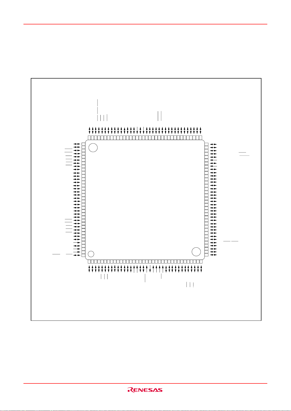
Pin configuration
Fig. AA-1 shows the pin configuration (top view).
PIN CONFIGURATION (top view)
11
/CLKS
11
/RTS
11
11
11
11
D
D
X
X
/T
/CTS
/CLK
/R
71
81
91
101
/INT
/INT
/INT
/INT
4
5
6
3
P97/AD
P125/INT
P124/INT
P123/INT
P122/INT
P121/INT
P120/INT
P111/F1
P110/F1
P107/AN7/INT
P106/AN6/INT
P105/AN5/INT
P104/AN4/INT
P103/AN3/INT
P102/AN
P101/AN
P100/AN
TRG/SIN40
/INT
P1
P12
P0
P0
P0
P0
P0
P0
P0
P0
P11
P11
P11
P11
P11
P11
OUT1
OUT0
AV
V
AVcc
1
2
P1
P1
P1
108
106
107
0
109
6
110
111
111
112
102
113
92
114
82
115
72
116
61
117
7
118
6
119
5
120
4
121
3
122
2
123
1
124
0
125
7
126
6
127
5
128
4
129
3
130
2
131
132
133
110
100
134
135
90
80
136
137
70
138
2
139
1
140
SS
141
0
142
REF
143
60
144
1 2 3 4 5 6 7 8 910111213141516171819202122232425
0
1
7
P1
P1
P1
P2
P2
P1
100
101
104
105
102
103
M306KAFCLRP
41
/PWM
51
00
/OBF
/PWM
0OUT
5
P13
77
6
P13
76
7
P13
75
TA0
/
0
P4
74
0OUT
/TA1
1
P4
73
72
P4
71
P43/OBF01/SERIRQ
70
P44/PWM01/OBF
69
P4
68
P46/PWM21/OBF3/CLKRUN
V
67
66
65
64
63
62
61
60
59
58
57
56
55
54
53
52
51
50
49
48
47
46
45
44
43
42
41
40
39
38
37
CC
P4
V
SS
P140/KI
P141/KI
P142/KI
P143/KI
P144/KI
P145/KI
P146/KI
P147/KI
P5
P5
P5
P5
P5
P5
P5
P5
P150/TA0
P151/TA1
P152/TA2
P60/SDA
P61/SCL
P62/SDA
P63/SCL
P64/CTS10/RTS10/CLKS
P65/CLK
P66/RXD10/TA3
P67/TXD10/TA4
P70/PS2A
2
/TA2
0OUT/GATEA20
31
10
11
12
13
14
15
16
17
00
01
02
03
04
05
06
OUT
1OUT
1OUT/SIN31
1OUT/SOUT31
0
0
10
10
10
0
1
/KI
07
/CLK
OUT
OUT
5
/PWM11/OBF2/PRST
7
/PWM
0
/KI
/KI
1
/KI
2
/KI
3
/KI
4
/KI
5
/KI
6
/CLK
7
31
10
1
2
0
/LAD
6
7
4
2
3
5
0
SS
P2
P2
V
P2
P2
P2
P2
P3
92
93
94
96
97
95
98
99
3
7
/LAD
/LFRAME
/LRESET
/LCLK
/LAD
/LAD
1
4
5
6
2
3
CC
P12
P3
P3
V
88
89
90
91
7
P3
P3
P3
P3
P3
84
85
86
87
83
26 27 28 29 30 31 32 33 34 35 36
0
P13
82
1
P13
81
2
P13
80
3
P13
79
4
P13
78
10
00
30
20
/PWM
/PWM
/PWM
/PWM
40
0IN
0IN
OUT40
/TB4
/TB3
4
3
P9
P9
/ANEX0/CLK
/ANEX1/S
5
6
P9
P9
Fig. AA-1 Pin configuration (top view)
Rev.1.00 Jul 16, 2004 page 4 of 266
REJ03B0100-0100Z
5
/INT
OUT30
/S
2
P9
4
/INT
IN30
/S
1
P9
3
/INT
30
/CLK
0
P9
40
50
/PWM
/PWM
1IN
1IN
/TB3
/TB4
0
1
P16
P16
IN41
/S
7
P15
OUT41
/S
6
P15
41
/CLK
5
P15
4
P15
3
P15
0
7
1
6
IN
SS
OUT
X
RESET
CC
X
V
V
M
M
P8
P8
/NMI
5
P8
21
/SCL
IN
/TB2
4
P8
21
/SDA
IN
/TB1
3
P8
11
/SCL
IN
/TB0
2
P8
11
/SDA
IN
/TA4
1
P8
20
/ICCK
0
/SCL
IN
P8
/TA3
7
P7
20
/SDA
6
P7
1
2
/PS2B
/PS2B
1
2
/INT
/INT
4
IN
P7
/TA2
5
P7
2
0
/PS2A
/PS2B
2
0
P7
/INT
IN
/TA1
3
P7
1
/PS2A
IN
/TB5
IN
/TA0
1
P7
Package: 144PFB-A
Page 5
M16C/6KA Group Description
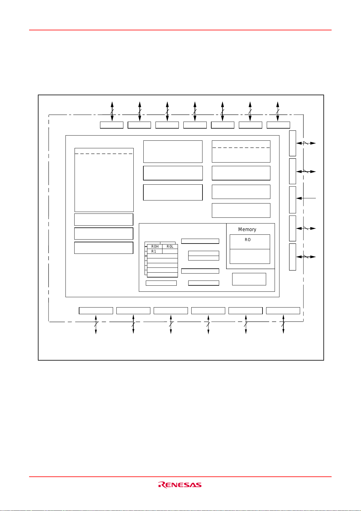
Block Diagram
Fig.AA-2 is a block diagram of the M16C/6KA (144-pin version) group.
I/O ports
Internal peripheral function
Timer
Timer TA0(16 bits)
Timer TA1(16 bits)
Timer TA2(16 bits)
Timer TA3(16 bits)
Timer TA4(16 bits)
Timer TB0(16 bits)
Timer TB1(16 bits)
Timer TB2(16 bits)
Timer TB3(16 bits)
Timer TB4(16 bits)
Timer TB5(16 bits)
Watchdog timer
(15 bits)
PS2 interface
(3 channels)
Serial interrupt output
(6 factors)
Port P0
8
Port P18Port P2
8 8 8 8
A-D converter
(10 bits x 8 channels
Expandable up to 10 channels)
UART/clock synchronous SI/O
(8 bits x 1 channel)
Host interface
(LPC bus interface
x
4 channels)
M16C/60 series 16-bit CPU core
Registers
R0H
R1H R1
R1H R1L
R
R2
R
2
R3
A
3
A0
A
0
A1
FB
1
FB
SB
R0
R0LR0H
L
L
Program counter
PC
Stack pointer
ISP
USP
Vector table
INTB
Flag register
FLG
Port P5Port P4Port P3
System clock generator
IN-XOUT
X
Clock synchronous SI/O
(8 bits x 2channels)
2
I C bus interface
(3 channels)
PWM output
(8 bits x 6channels)
Memory
ROM
(Note1)
RAM
(Note2)
Multiplier
8
Port P6
Port P7
8
Port P8
7
Port P8
5
Port P9
8
Port P10
8
Port P16
2
Note1 : ROM size depends on MCU type.
Note2 : RAM size depends on MCU type.
Port P15
8
Port P14
8
Fig.AA-2 Block diagram of M16C/6KA (144-pin version) group
Rev.1.00 Jul 16, 2004 page 5 of 266
REJ03B0100-0100Z
Port P13
8
Port P12
8
Port P11
8
Page 6

M16C/6KA Group Description
Performance Outline
Table AA-1 is a performance outline of M16C/6KA (144-pin version) group.
Table AA-1 Performance outline of M16C/6KA (144-pin version) group
Item Performance
Number of basic instructions 91 instructions
The Min. time of instruction execution 62.5ns (f(XIN)=16MHz, with 0 wait, Vcc=3.3V)
Memory ROM (See the figure of ROM Expansion)
capacity RAM 5K bytes
I/O port P0 to P10 (except P85) 8 bits x 10, 7 bits x 1
P11 to P16 8 bitsx5, 2 bitsx1
Input port P85 1 bit x 1
Multifunction TA0, TA1, TA2, TA3, TA4 16 bits x 5
timer TB0, TB1, TB2, TB3, TB4, TB5 16 bits x 6
Serial I/O UART1 (UART or clock synchronous) x 1
SI/O3, SI/O4 (Clock synchronous) x 2
A-D converter 10 bits x (8 + 2) channels
Watchdog timer 15 bits x 1 (with prescaler)
Interrupt 32 internal and 16 external sources, 4 software
sources, 7 levels
Host interface 4 channels (LPC bus interface)
PWM 8 bits x 6
I2C bus interface 3 channels
PS2 interface 3 channels
Serial interrupt output 6 factors (2 fixed factors, 4 programmable factors)
Clock generating circuit 1 built-in clock generation circuit
(built-in feedback resistor, and external ceramic)
Power consumption 52.8mW (3.3V, f(XIN)=16MHz, with 0 wait)
I/O I/O withstand voltage 3.3V
characteristics Output current 5mA
Device configuration CMOS high performance silicon gate
Package 144-pin plastic mold QFP
Rev.1.00 Jul 16, 2004 page 6 of 266
REJ03B0100-0100Z
Page 7
M16C/6KA Group Description
Renesas plans to release the following products in the M16C/6KA (144-pin version) group:
(1) Support for flash memory version
(2) ROM capacity
(3) Package
144PFB-A : Plastic molded QFP(flash memory version)
ROM Size
(Byte)
External
ROM
256K
128K
96K
80K
64K
32K
Mask ROM version Flash version
M306KAFCLRP
Fig.AA-3 ROM expansion
Table AA-2 Product list From July 2004 up to now
Type No.
M306KAFCLRP
ROM size
128 bytes
RAM size
5K bytes
Package type
144PFB-A
Host Interface
LPC
Remarks
Flash memory (NEW
DINOR) version
Rev.1.00 Jul 16, 2004 page 7 of 266
REJ03B0100-0100Z
Page 8

M16C/6KA Group Description
Type No.
M30 6KA F C XXX RP
Fig.AA-4 Type No., memory size, and package
Package type
RP : 144PFB-A
ROM No.
ROM type
C : 128Kbytes
Memory type
F : Flash version
M16C/6KA Group
M16C Family
Rev.1.00 Jul 16, 2004 page 8 of 266
REJ03B0100-0100Z
Page 9

M16C/6KA Group Pin Description
Pin Description
Pin name
Vcc, Vss
____________
RESET
Signal name
Power supply
input
Reset input
I/O type
Input
Function
Apply 3.0 to 3.6 V to VCC . Apply 0V to VSS
A “L” on this input resets the microcomputer.
XIN
XOUT
M0,M1
AVCC
AVSS
VREF
P00 to P07
P10 to P17
P20 to P27
P30 to P37
P40 to P47
P50 to P57
Clock input
Clock output
Chip mode
setting
Analog power
supply input
Analog power
supply input
Reference
voltage input
I/O port P0
I/O port P1
I/O port P2
I/O port P3
I/O port P4
I/O port P5
Input
Output
Input
Input
Input/output
Input/output
Input/output
Input/output
Input/output
Input/output
These pins are provided for the main clock generating circuit.
Connect a ceramic resonator between the XIN and the XOUT
pins. To use an externally derived clock, input it to the XIN pin
and leave the XOUT pin open.
Connect to VSS
This pin is a power supply input for the A-D converter.
Connect this pin to VCC.
This pin is a power supply input for the A-D converter.
Connect this pin to VSS.
This pin is a reference voltage input for the A-D converter.
This is an 8-bit CMOS I/O port. It has an input/output port
direction register that allows the user to set each pin for input or output individually. When set for input, the user can
specify in units of four bits via software whether or not they
are tied to a pull-up resistor.
This port supports CMOS input level. And output type supports CMOS 3 state or N channel open drain selectable.
This is an 8-bit I/O port equivalent to P0. Pins in this port also
function as external interrupt pins or UART1 I/O pin selected
by software.
This is an 8-bit I/O port equivalent to P0. (Except that output
type just supports CMOS 3 state only). P20-P27 are available for directly driving LED's.
This is an 8-bit I/O port equivalent to P0. (Except that output
type just supports CMOS 3 state only). The port can be
used for LPC bus interface I/O pins by software selection.
This is an 8-bit I/O port equivalent to P0. (Except that output
type just supports CMOS 3 state only). By software selecting,
the port can also be used for LPC bus interface I/O pins,
Timer A0 to A2 output pins PWM output pins or serial interrupt
output I/O pins. P40 to P46 pins' level can be read regardless
the setting of input port or output port. If P40 or P43 are used
for output ports, the function that clears P40 or P43 to "0" after
the read of output data buffer from host CPU is available.
This is an 8-bit I/O port equivalent to P0. (Except that output type
is CMOS 3 state only). Key on wake interrupt 0 input function
support. P57 in this port outputs a divide-by-8 or divide-by-32
clock of XIN selected by software.
Rev.1.00 Jul 16, 2004 page 9 of 266
REJ03B0100-0100Z
Page 10

M16C/6KA Group Pin Description
Pin Description
Pin name
P60 to P67
P70 to P77
P80 to P84,
P86,
P87,
P85
P90 to P97
P100 to P107
Signal name
I/O port P6
I/O port P7
I/O port P8
I/O port P85
I/O port P9
I/O port P10
I/O type
Input/output
Input/output
Input/output
Input/output
Input/output
Input
Input/output
Input/output
Function
This is an 8-bit I/O port equivalent to P0. (Except that P60 to
P63's output type is N channel open drain only; P64 to P67's
output type is CMOS 3 state only; P60 to P63 no internal
pull-up register support.) By software selecting, this port
can be used for I2C-BUS interface, UART1 input/output pin,
timerA3, A4 output pin. When P60 to P63 used as I2C-BUS
interface SDA, SCL, the input level of these pins are CMOS/
SMBUS selectable.
This is an 8-bit I/O port equivalent to P0. (Except that P70 to
P77 output type is N channel open drain only; no internal
pull-up register support.) By software selecting, this port
can be used for external interrupt input pin, timerA0 to A3
and timer B5 input pin, PS2 interface input/output pin, I2C
interface input/output pin. P70 to P75 pins' level can be read
regardless of the setting of input port or output port.
P80 to P84, P86, and P87 are I/O ports with the same functions as P0. (Except that P86 to P87's output type is CMOS
3 state only; P80 to P84's output type is N channel open
drain only; P85 is input port only; the P80 to P84 and P85 are
no internal pull-up register support.)
By software selecting, this port can be used for timer A4, B0
to B2, I2C-BUS interface I/O pins. The input level of P81 to
P84 and SDA, SCL inputs can be switched to CMOS/SMBUS
when these pins function as I2C bus interface. P85 is an
______ ______
input-only port that also functions for NMI. The NMI interrupt
is generated when the input at this pin changes from “H” to
______
“L”. The NMI function cannot be cancelled using software.
This is an 8-bit I/O port equivalent to P0. (Except that output
type is CMOS 3 state only.) By software selecting, the port
can be used for external interrupt, timer B3 to B4, A-D converter extended input pins, A-D trigger, SI/O3, SI/O4 I/O
pins, PWM, output pins.
This is an 8-bit I/O port equivalent to P0. (Except that output
type is CMOS 3 state only.) If the ports are set to input
mode, the pull-up resistor can be set in bit unit. By software
selecting, the port can be used for A-D converter, external
interrupt input pins.
Rev.1.00 Jul 16, 2004 page 10 of 266
REJ03B0100-0100Z
Page 11

M16C/6KA Group Pin Description
Pin Description
Pin name
P110 to P117
P120 to P127
P130 to P137
P140 to P147
P150 to P157
P160, P161
Signal name
I/O port P11
I/O port P12
I/O port P13
I/O port P14
I/O port P15
I/O port P16
I/O type
Input/output
Input/output
Input/output
Input/output
Input/output
Input/output
Function
This is an 8-bit I/O port equivalent to P0. By software selecting, P110, P111 also function as clock output pins, which the
frequency is the same with XIN.
This is an 8-bit I/O port equivalent to P0. (Except that outp u t
type is CMOS 3 state only.) By software selecting, this port
can be used for external interrupt input pin.
This is an 8-bit I/O port equivalent to P0. (Except that output
type is N channel open drain only; no internal pull-up register support.)
This is an 8-bit I/O port equivalent to P0. The port can be
used for key on wake-up interrupt 1 input pins. P140 to P143
are available for directly driving LED's. In input mode, the
pull-up register can be set in one bit unit by software.
This is an 8-bit I/O port equivalent to P0. (Except that output
type is CMOS 3 state only.) By software selecting, these
ports can be used for timer A0 to A2's output or SI/O3 and
SI/O4 I/O pins.
This is an 2-bit I/O port equivalent to P0. (Except that output
type is CMOS 3 state only.) By software selecting, this port
can be used for timer B3 and B4 input or PWM output pin.
Rev.1.00 Jul 16, 2004 page 11 of 266
REJ03B0100-0100Z
Page 12
M16C/6KA Group Memory
Operation of Functional Blocks
The M16C/6KA (144-pin version) group accommodates certain units in a single chip. These units include
ROM and RAM to store instructions and data and the central processing unit (CPU) to execute arithmetic/
logic operations. Also peripheral units such as timers, serial I/O, A-D converter, host bus interface, PWM
output, I2C BUS interface, PS2 interface and I/O ports are included.
The following explains each unit.
Memory
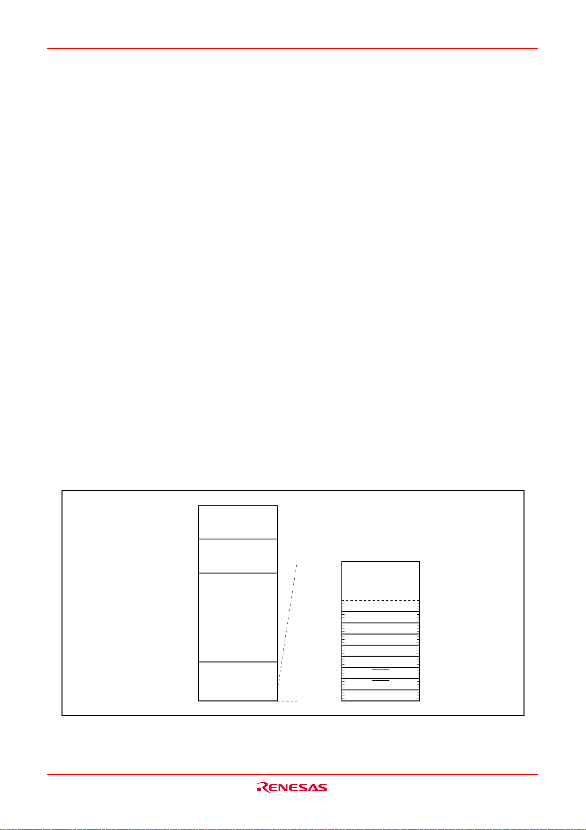
Fig.CA-1 is the memory map. The address space extends up to 1M bytes from address 0000016 to FFFFF16.
There is 128K bytes of internal ROM from E000016 to FFFFF16. The vector table for fixed interrupts such as
the reset and NMI are mapped from FFFDC16 to FFFFF16. The starting address of the interrupt routine is
stored here. The address of the vector table for timer interrupts, etc., can be set as desired using the internal
register (INTB). See the section on interrupts for details.
From 0040016 to the address increasing direction RAM is allocated. For example, in the M306KAFCLRP, 5K
bytes of internal RAM is mapped to the space from 0040016 to 017FF16. In addition to storing data, the RAM
also stores the stack used when calling subroutines and when interrupts are generated.
The SFR area is mapped from 0000016 to 003FF16. This area accommodates the control registers for peripheral devices such as I/O ports, A-D converter, serial I/O, and timers, etc. Fig.CA-2 to CA-5 are location of
peripheral unit control registers. Any part of the SFR area that is not occupied is reserved and cannot be
used for other purposes.
The special page vector table is mapped from FFE0016 to FFFDB16. If the starting addresses of subroutines
or the destination addresses of jumps are stored here, subroutine call instructions and jump instructions can
be used as 2-byte instructions, reducing the number of program steps.
_______
00000
16
0040016
017FF16
E000016
FFFFF16
Fig.CA-1 Memory map
Rev.1.00 Jul 16, 2004 page 12 of 266
REJ03B0100-0100Z
SFR area
For details, see
Fig.CA-2 to Fig.CA-4
Internal RAM area
Inhibited
Internal ROM area
FFE0016
FFFDC16
FFFFF16
Special page
vector table
Undefined instruction
Overflow
BRK instruction
Address match
Single step
Watchdog timer
DBC
NMI
Reset
Page 13
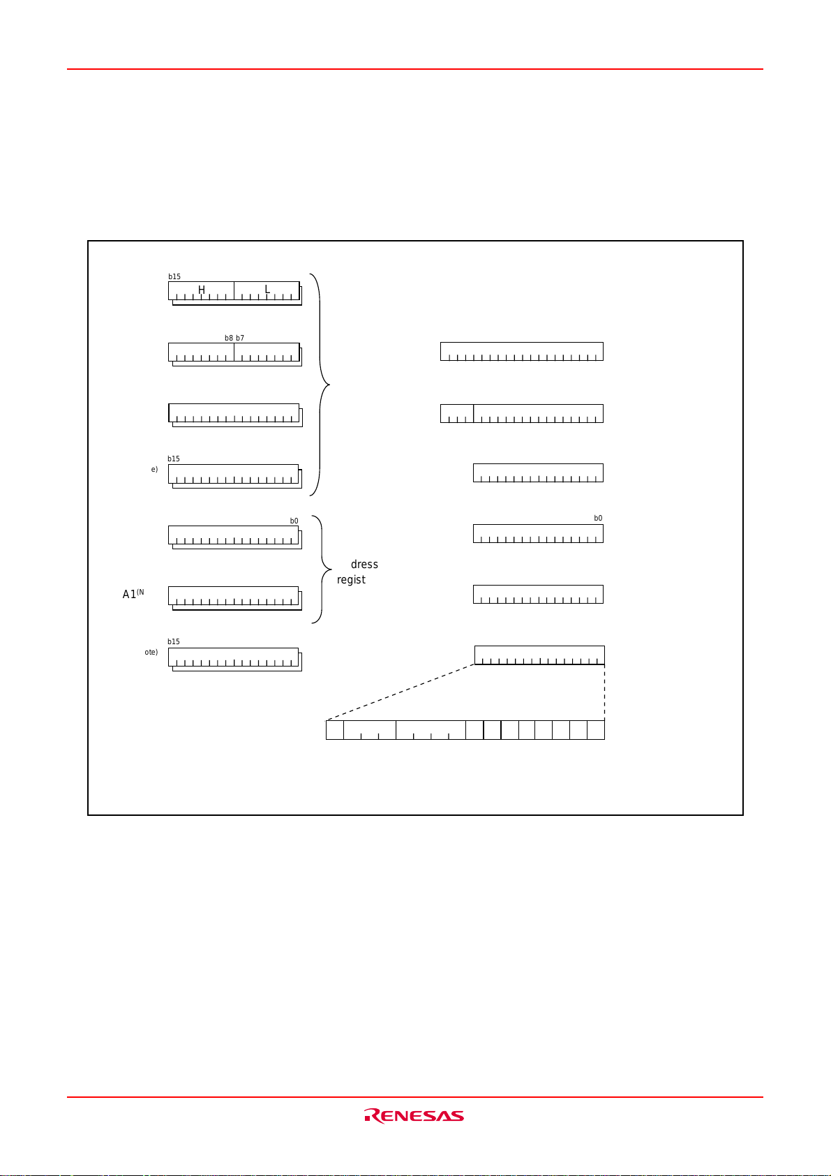
M16C/6KA Group CPU
A
Central Processing Unit (CPU)
The CPU has a total of 13 registers shown in Fig.BA-1 Seven of these registers (R0, R1, R2, R3, A0, A1, and
FB) come in two sets; therefore, these have two register banks.
R0
R1
R2
R3
A0
A1
FB
(Note)
(Note)
(Note)
(Note)
(Note)
(Note)
(Note)
b15
b15
b15
b15
b15
b15
b15
b8 b7 b0
H
b8 b7 b0
H
L
b19
L
PC
b0
Program counter
Data
b0
registers
INTB
b19
H
b0
L
Interrupt table
register
b0
b0
b15
USP
b15
ISP
b0
User stack pointer
b0
Interrupt stack
pointer
Address
b0
registers
b15
SB
b0
Static base
register
b0
Frame base
b15
FLG
b0
Flag register
register
IPL
CDZSBOIU
Note: These registers consist of two register banks.
Fig.BA-1 Central processing unit register
(1) Data registers (R0, R0H, R0L, R1, R1H, R1L, R2, and R3)
Data registers (R0, R1, R2, and R3) are configured with 16 bits, and are used primarily for transfer and
arithmetic/logic operations.
Registers R0 and R1 each can be used as separate 8-bit data registers, high-order bits as (R0H/R1H), and
low-order bits as (R0L/R1L). In some instructions, registers R2 and R0, as well as R3 and R1 can use as 32bit data registers (R2R0/R3R1).
(2) Address registers (A0 and A1)
Address registers (A0 and A1) are configured with 16 bits, and have functions equivalent to those of data
registers. These registers can also be u2sed for address register indirect addressing and address register
relative addressing.
In some instructions, registers A1 and A0 can be combined for use as a 32-bit address register (A1A0).
Rev.1.00 Jul 16, 2004 page 13 of 266
REJ03B0100-0100Z
Page 14

M16C/6KA Group CPU
(3) Frame base register (FB)
Frame base register (FB) is configured with 16 bits, and is used for FB relative addressing.
(4) Program counter (PC)
Program counter (PC) is configured with 20 bits, indicating the address of an instruction to be executed.
(5) Interrupt table register (INTB)
Interrupt table register (INTB) is configured with 20 bits, indicating the start address of an interrupt vector
table.
(6) Stack pointer (USP/ISP)
Stack pointer comes in two types: user stack pointer (USP) and interrupt stack pointer (ISP), each configured
with 16 bits.
Your desired type of stack pointer (USP or ISP) can be selected by a stack pointer select flag (U flag). This
flag is located at the position of bit 7 in the flag register (FLG).
(7) Static base register (SB)
Static base register (SB) is configured with 16 bits, and is used for SB relative addressing.
(8) Flag register (FLG)
Flag register (FLG) is configured with 11 bits, each bit is used as a flag. Fig.BA-2 shows the flag register
(FLG). The following explains the function of each flag:
• Bit 0: Carry flag (C flag)
This flag retains a carry, borrow, or shift-out bit that has occurred in the arithmetic/logic unit.
• Bit 1: Debug flag (D flag)
This flag enables a single-step interrupt.
When this flag is “1”, a single-step interrupt is generated after instruction execution. This flag is cleared to
“0” when the interrupt is acknowledged.
• Bit 2: Zero flag (Z flag)
This flag is set to “1” when an arithmetic operation resulted in 0; otherwise, cleared to “0”.
• Bit 3: Sign flag (S flag)
This flag is set to “1” when an arithmetic operation resulted in a negative value; otherwise, cleared to “0”.
• Bit 4: Register bank select flag (B flag)
This flag chooses a register bank. Register bank 0 is selected when this flag is “0” ; register bank 1 is
selected when this flag is “1”.
• Bit 5: Overflow flag (O flag)
This flag is set to “1” when an arithmetic operation resulted in overflow; otherwise, cleared to “0”.
• Bit 6: Interrupt enable flag (I flag)
This flag enables a maskable interrupt.
An interrupt is disabled when this flag is “0”, and is enabled when this flag is “1”. This flag is cleared to “0”
when the interrupt is acknowledged.
Rev.1.00 Jul 16, 2004 page 14 of 266
REJ03B0100-0100Z
Page 15
M16C/6KA Group CPU
• Bit 7: Stack pointer select flag (U flag)
Interrupt stack pointer (ISP) is selected when this flag is “0” ; user stack pointer (USP) is selected when this
flag is “1”.
This flag is cleared to “0” when a hardware interrupt is acknowledged or an INT instruction of software
interrupt No. 0 to 31 is executed.
• Bits 8 to 11: Reserved area
• Bits 12 to 14: Processor interrupt priority level (IPL)
Processor interrupt priority level (IPL) is configured with the three bits, for specification of up to eight processor interrupt priority levels from level 0 to level 7.
If a requested interrupt has priority greater than the processor interrupt priority level (IPL), the interrupt is
enabled.
• Bit 15: Reserved area
The C, Z, S, and O flags are changed when instructions are executed. See the software manual for details.
IPL
b0b15
Flag register (FLG)
CDZSBOIU
Carry flag
Debug flag
Zero flag
Sign flag
Register bank select flag
Overflow flag
Interrupt enable flag
Stack pointer select flag
Reserved area
Processor interrupt priority level (CPU)
Reserved area
Fig.BA-2 Flag register (FLG)
Rev.1.00 Jul 16, 2004 page 15 of 266
REJ03B0100-0100Z
Page 16
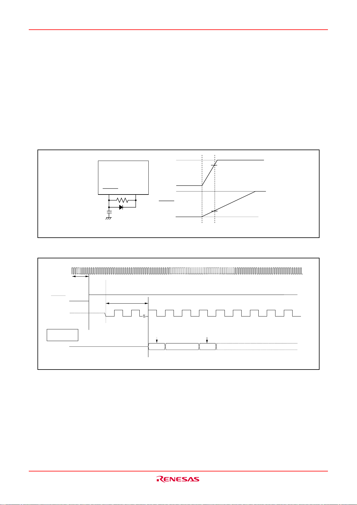
M16C/6KA Group RESET
Reset
There are two kinds of resets; hardware and software. In both cases, operation is the same after the reset.
(See “Software Reset” for details of software resets.) This section explains the hardware reset.
When the supply voltage is in the range where operation is guaranteed, a reset is effected by holding the
reset pin level “L” (0.2VCC max.) for at least 20 cycles. When the reset pin level is then returned to the “H”
level while main clock is stable, the reset status is cancelled and program execution resumes from the
address in the reset vector table.
Fig.VB-1 shows the example reset circuit. Fig.VB-2 shows the reset sequence.
RESET
Example when V
Fig.VB-1 Example reset circuit
X
IN
More than 20 cycles are needed
RESET
Internal
clock Φ
Single chip
mode
Address
BCLK 24cycles
V
CC
CC
= 3.3V
RESET
FFFFC
3.3V
V
CC
0V
3.3V
0V
16
FFFFE
3.0V
0.6V
Content of reset vector
16
Fig.VB-2 Reset sequence
Rev.1.00 Jul 16, 2004 page 16 of 266
REJ03B0100-0100Z
Page 17

M16C/6KA Group RESET
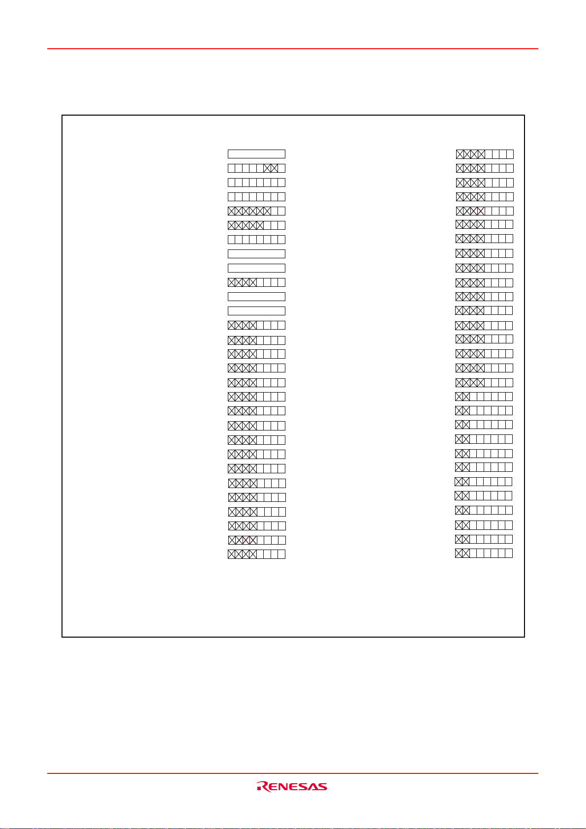
Table VB-1 shows the statuses of the other pins while the RESET pin level is “L”. Fig.VB-3 and VB-4 show
____________
the internal status of the microcomputer immediately after the reset is cancelled.
Table VB-1 Pin status when RESET pin level is “L”
____________
Status
Pin name
P0
P1
P2, P3, P4
P4
4
P45 to P4
P5
0
P5
1
P5
2
0
7
to P4
I/O port (floating)
I/O port (floating)
3
I/O port (floating)
I/O port (floating)
I/O port (floating)
I/O port (floating)
I/O port (floating)
I/O port (floating)
CNVSS = V
(M0)
SS
P5
3
P5
4
P5
5
P5
6
P5
7
P6, P7, P80 to P84,
P86, P87, P9, P10
P11, P12, P13, P14
P15, P16
I/O port (floating)
I/O port (floating)
I/O port (floating)
I/O port (floating)
I/O port (floating)
I/O port (floating)
I/O port (floating)
I/O port (floating)
Rev.1.00 Jul 16, 2004 page 17 of 266
REJ03B0100-0100Z
Page 18
M16C/6KA Group RESET
(1) (0004
(2) (000516)···Processor mode register 1
(3) (0006
(4) (0007
(5) (0009
Protect register (000A
(6)
(7)
(8) (0010
(9)
(10)
(11)
(12)
(13)
(14)
(15)
Timer A0 interrupt control register
(16)
(17)
(18)
Timer A3 interrupt control register
(19)
(20)
Timer A4 interrupt control register (004E
Timer B0 interrupt control register (004F
(21)
Timer B1 interrupt control register (0050
(22)
(23)
Timer B2 interrupt control register
(24)
Timer B3 interrupt control register
Timer B4 interrupt control register
(25)
(000F16)···Watchdog timer control register
(0011
(0012
(0014
(0015
(0016
(0041
(0044
(0045
(0046
(0047
(0048
(004A
(004B
(004C
(004D
(0051
(0052
(0053
16
)···Processor mode register 0
10000100
16
)···System clock control register 0
00010000
16
)···System clock control register 1
16
)···Address match interrupt enable register
16
)···
00?0????
16
)···Address match interrupt register 0
16
)···
16
)···
16
)···Address match interrupt register 1
16
)···
16
)···
16
)···LRESET interrupt control register
16
)···A-D interrupt control register
16
)···IBF0 interrupt control register
16
)···IBF1 interrupt control register
16
)···IBF2 interrupt control register
16
)···IBF3 interrupt control register
16
)···
16
)···Timer A1 interrupt control register
16
)···Timer A2 interrupt control register
16
)···
16
)···
16
)···
16
)···
16
)···
16
)···
16
)···
00
16
000
00
16
00
16
0
00
16
00
16
0
?000
?000
?000
?000
?000
?000
? 000
? 000
? 0 0 0
? 0 0 0
? 0 0 0
? 0 0 0
? 0 0 0
? 000
? 0 0 0
000
0 0 0
0 0 0
000?
(26)
Timer B5 interrupt control register (0054
000
(27)
OBE interrupt control register
(28)
PS20 interrupt control register (0056
PS21 interrupt control register
(29)
(30)
00
PS22 interrupt control register
(31)
UART1 receive interrupt control register
UART1 transmit interrupt control register
(32)
(33)
Key input 0 interrupt control register
(34)
Key input 1 interrupt control register
(35)
SI/O3 interrupt control register
(36)
SI/O4 interrupt control register
2
(37)
C0 interrupt control register
I
(38)
SCL0, SDA0 interrupt control register
2
(39)
C1 interrupt control register
I
(40)
SCL1, SDA1 interrupt control register
2
(41)
C2 interrupt control register
I
(42)
SCL2, SDA2 interrupt control register
(43)
INT0 interrupt control register
(44)
INT1 interrupt control register
(45)
INT2 interrupt control register
(46)
INT3 interrupt control register
(47)
INT4 interrupt control register
(48)
INT5 interrupt control register (006E16)···
(49)
INT6 interrupt control register
(50)
INT7 interrupt control register
(51)
INT8 interrupt control register
(52)
INT9 interrupt control register
(53)
INT10 interrupt control register
(54)
INT11 interrupt control register
(0055
(0057
(0058
(005B
(005C
(005F
(0060
(0061
(0062
(0063
(0064
(0065
(0066
(0067
(0068
(0069
(006A
(006B
(006C
(006D
(006F
(0070
(0071
(0072
(0073
(0074
16
)···
16
)···
16
)···
16
)···
16
)···
16
)···
16
)···
16
)···
16
)···
16
)···
16
)···
16
)···
16
)···
16
)···
16
)···
16
)···
16
)···
16
)···
16
)···
16
)···
16
)···
16
)···
16
)···
16
)···
16
)···
16
)···
16
)···
16
)···
00
00
00
00
00
00
00
00
00
00
00
00
? 000
? 0 0 0
? 0 0 0
? 0 0 0
? 000
? 000
? 000
? 0 0 0
? 000
? 000
? 000
? 000
? 000
? 000
? 000
? 000
? 000
? 000
? 000
? 000
? 000
? 000
? 000
? 000
? 000
? 000
? 000
? 000
? 000
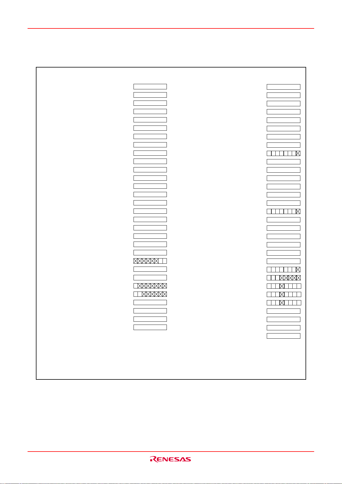
x : Nothing is mapped to this bit
? : Undefined
The content of other registers and RAM is undefined when the microcomputer is reset. The initial values must therefore be set.
Fig.VB-3 Device's internal status after a reset is cleared (1)
Rev.1.00 Jul 16, 2004 page 18 of 266
REJ03B0100-0100Z
Page 19
M16C/6KA Group RESET
(55)
(56)
(57)
(58)
(59)
(60)
PS21 control register (02A6
(61)
(62)
(63)
PS22 control register
(64)
PS2 mode register
(65)
Data bus buffer status register 1
(66)
(67)
Data bus buffer status register 2
(68)
(69)
(70)
GateA20 control register
(71)
Port P11 direction register
(72)
Port P12 direction register
(73)
Port P13 direction register
(74)
Port P14 direction register
(75)
Port P15 direction register
(76)
Port P16 direction register
(77)
Port function selection register 0
(78)
Port function selection register 1
(79)
Port P4 input register
(80)
Port P7 input register
(81)
Pull-up control register 3
(82)
Pull-up control register 4
(83)
Port control register 1
(84)
Port control register 2
(02A0
16
(02A116)···PS20 status register
16
(02A2
16
(02A4
16
(02A5
16
16
(02A8
(02A916)···PS22 status register
16
)···
(02AA
16
(02AC
16
(02C1
(02C3
16
16
(02C5
(02C716)···Data bus buffer status register 3
16
(02C9
(02CA
16
16
(02E2
(02E3
16
(02E616)···
16
(02E7
(02EA
16
)···
(02EB
16
)···
(02F8
16
)···
16
)···
(02F9
(02FA
16
16
(02FB
16
(02FC
16
(02FD
16
(02FE
16
(02FF
00
0
00
16
00
16
00
16
00
16
00
16
00
16
00
16
00
16
00
16
00
16
00
16
00
16
00
16
00
16
00
16
00
16
00
16
00
16
00
16
00
16
00
16
0 0
00
16
00
16
00
16
00
16
00
16
00
16
PWM control register 0
(85)
PWM control register 1
(86)
2
I
C2 address register
(87)
2
C2 control register 0
I
(88)
2
I
C2 clock control register
(89)
2
C2 start/stop condition
I
(90)
control register
2
(91)
C2 control register 1
I
2
C2 control register 2
I
(92)
2
(93)
C2 status register
I
2
C0 address register
I
(94)
2
C0 control register 0
I
(95)
2
I
C0 clock control register
(96)
2
I
C0 start/stop condition
(97)
control register
2
I
C0 control register 1
(98)
2
I
C0 control register 2
(99)
2
C0 status register
I
(100)
2
C1 address register
I
(101)
2
C1 control register 0
I
(102)
2
C1 clock control register
I
(103)
2
C1 start/stop condition
I
(104)
control register
2
I
C1 control register 1
(105)
2
I
C1 control register 2
(106)
2
C1 status register
I
(107)
(108)
TimerB3,4,5 count start flag
TimerB3 mode register
(109)
(110)
TimerB4 mode register
(111)
TimerB5 mode register
(112)
Interrupt factor selection register 1
Interrupt factor selection register 0
(113)
(114)
SI/O3 control register
SI/O4 control register
(115)
(030C
(030D
(0312
(0313
(0314
(0315
(0316
(0317
(0318
(0322
(0323
(0324
(0325
(0326
(0327
(0328
(0332
(0333
(0334
(0335
(0336
(0337
(0338
(0340
(035B
(035C
(035D
(035E
(035F
(0362
(0366
16
)···
16
)···
16
)···
16
)···
16
)···
16
)···
16
)···
16
)···
16
)···
16
)···
16
)···
16
)···
16
)···
16
)···
16
)···
16
)···
16
)···
16
)···
16
)···
16
)···
16
)···
16
)···
16
)···
16
)···
16
)···
16
)···
16
)···
16
)···
16
)···
16
)···
16
)···
)···PS20 shift register
)···PS20 control register
)···PS21 shift register
)···PS21 status register
)···
)···PS22 shift register
)···
)···Data bus buffer status register 0
)···
)···
)···Data bus buffer control register 1
)···
)···
)···
)···
)···
)···
)···
)···
)···
)···
00
16
00
16
00
16
00
16
00
16
1A
16
30
16
00
16
00 00001
00
16
00
16
00
16
1A
16
30
16
00
16
00 1 0000
00
16
00
16
00
16
1A
16
30
16
00
16
00 1 0000
0 00
00 ? 0000
00 ? 0000
00 ? 0000
00
16
00
16
40
16
40
16
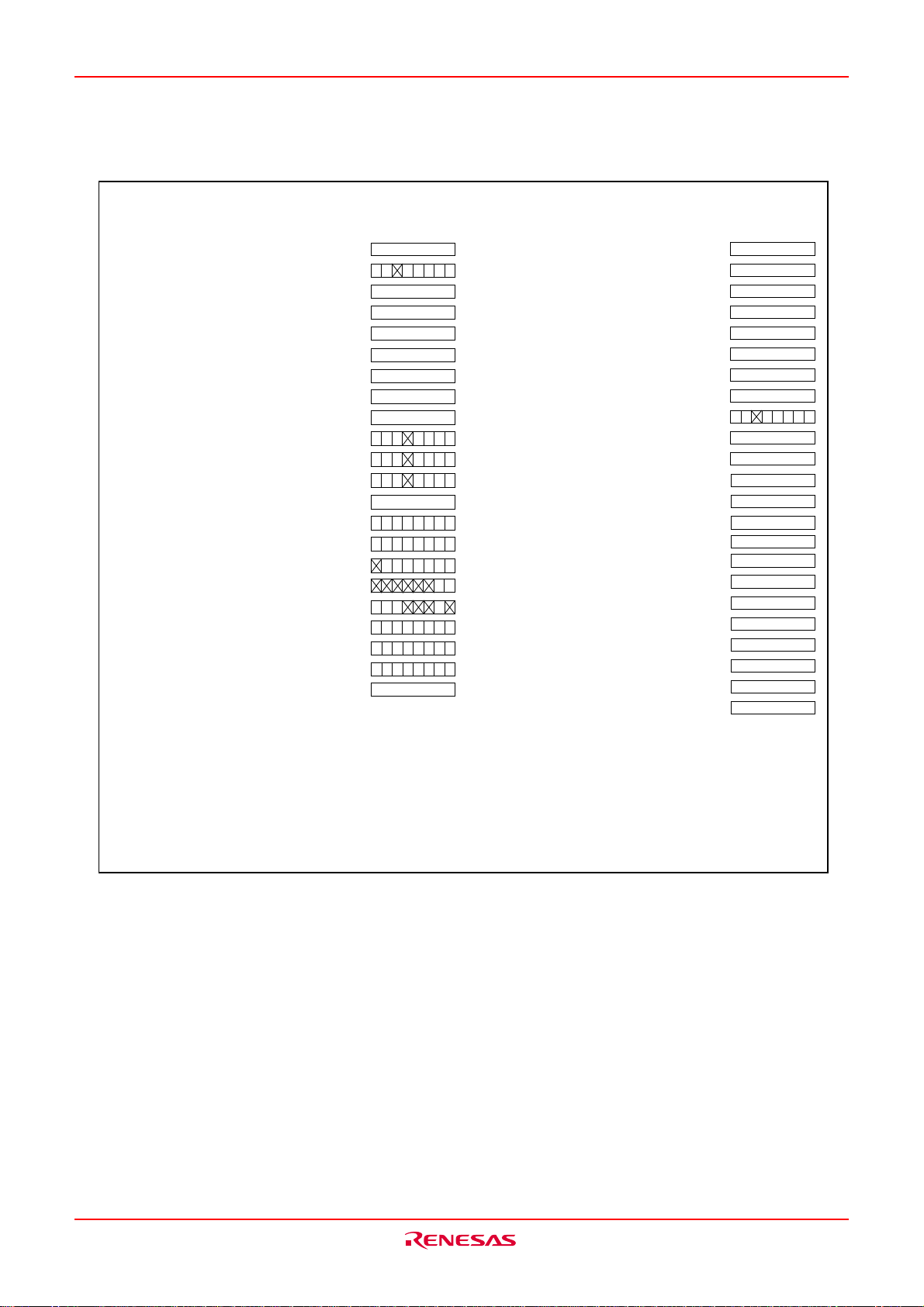
x : Nothing is mapped to this bit
? : Undefined
The content of other registers and RAM is undefined when the microcomputer is reset. The initial values must therefore be set.
Fig.VB-4 Device's internal status after a reset is cleared (2)
Rev.1.00 Jul 16, 2004 page 19 of 266
REJ03B0100-0100Z
Page 20
M16C/6KA Group RESET
Count start flag
(116)
One-shot start flag
(117)
Trigger select flag
(118)
(119)
Up-down flag
Timer A0 mode register
(120)
(121)
Timer A1 mode register
(122)
Timer A2 mode register
(123)
Timer A3 mode register
(124)
Timer A4 mode register
Timer B0 mode register
(125)
(126)
Timer B1 mode register
Timer B2 mode register
(127)
UART1 transmit/receive mode register
(128)
(129)
UART1 transmit/receive control register 0
(130)
UART1 transmit/receive control register 1
(131)
UART transmit/receive control register 2
Flash memory recognition register (Note1)
(132)
(133)
Flash memory control register1 (Note1)
(134)
Flash memory control register0 (Note1)
(135)
A-D control register 2
A-D control register 0
(136)
A-D control register 1
(137)
(038016)···
(0382
16)···
16)···
(0383
(0384
16)···
(0396
16)···
(0397
16)···
16)···
(0398
16)···
(0399
(039A
16)···
(039B
16)···
16)···
(039C
16)···
(039D
(03A8
16)···
16)···
(03AC
16)···
(03AD
(03B0
16)···
16)···
(03B4
(03B5
16)···
16)···
(03B7
16)···
(03D4
(03D6
16)···
16)···
(03D7
0016
0000000
0016
0016
0016
0016
0016
0016
0016
0
0? 0000
00? 0000
00? 0000
0016
000 1000
0
000 0010
0
0
000000
1
0
00
0
000010
0
0
000 00001
000 0???0
0016
(03E2
(03E3
(03E6
(03E7
(03EA
(03EB
(03EE
(03EF
(03F2
(03F3
(03F6
(03FC
(03FD
(03FE
(03FF
16)···
16)···
16)···
16)···
16)···
16)···
16)···
16)···
16)···
16)···
16)···
16)···
16)···
16)···
16)···
Port P0 direction register
(138)
Port P1 direction register
(139)
Port P2 direction register
(140)
Port P3 direction register
(141)
Port P4 direction register
(142)
Port P5 direction register
(143)
Port P6 direction register
(144)
Port P7 direction register
(145)
Port P8 direction register
(146)
(147)
Port P9 direction register
Port P10 direction register
(148)
(149)
Pull-up control register 0
(150)
Pull-up control register 1
Pull-up control register 2
(151)
Port control register 0
(152)
(153)
Data registers (R0/R1/R2/R3)
(154)
1
Address registers (A0/A1)
Frame base register (FB)
(155)
Interrupt table register (INTB)
(156)
(157)
User stack pointer (USP)
(158)
Interrupt stack pointer (ISP)
(159)
Static base register (SB)
(160)
Flag register (FLG)
0016
0016
0016
0016
0016
0016
0016
0016
00 00000
0016
0016
0016
0016
0016
0016
000016
000016
000016
0000016
000016
000016
000016
000016
x : Nothing is mapped to this bit
? : Undefined
The content of other registers and RAM is undefined when the microcomputer is reset. The initial values must therefore be set.
(Note1) This register exists only in the flash memory version.
Fig.VB-5 Device's internal status after a reset is cleared (3)
Rev.1.00 Jul 16, 2004 page 20 of 266
REJ03B0100-0100Z
Page 21

M16C/6KA Group RESET
Serial interrupt control register 0
(161)
(162)
Serial interrupt control register 1
(163)
IRQ request register 0
(164)
IRQ request register 1
(165)
IRQ request register 2
(166)
IRQ request register 3
(167)
IRQ request register 4
Serial interrupt control register 2
(168)
LPC1 address register L
(169)
(170)
LPC1 address register H
LPC2 address register L
(171)
(172)
LPC2 address register H
LPC3 address register L
(173)
(174)
LPC3 address register H
(175)
LPC control register
Port function selection register 2
(176)
(177)
Pull-up resistor control register 5
Pull-up resistor control register 6
(178)
(179)
Key input interrupt 1 enable register
(180)
Key input interrupt 1 edge selection register
P14 event register
(181)
Port control register 3
(182)
16
(02B0
(02B116)···
16
(02B2
(02B3
16
16
(02B4
16
(02B5
(02B6
16
16
(02B7
(02D016)···
16
(02D1
16
(02D2
16
(02D3
(02D4
16
16
(02D5
16
(02D6
(02F116)···
(02F2
16
16
(02F3
16
(02F4
16
(02F5
16
(02F6
16
(02F7
00
)···
)···
)···
)···
)···
)···
)···
)···
)···
)···
)···
)···
)···
)···
)···
)···
)···
)···
)···
16
00
16
00
16
00
16
00
16
00
16
00
16
10
16
00
16
00
16
00
16
00
16
00
16
00
16
00
16
00
16
00
16
00
16
00
16
00
16
00
16
00
16
The content of other registers and RAM is undefined when the microcomputer is reset. The initial values must
therefore be set.
Fig.VB-6 Device's internal status after a reset is cleared (4)
Rev.1.00 Jul 16, 2004 page 21 of 266
REJ03B0100-0100Z
Page 22
M16C/6KA Group SFR
0000
16
0001
16
0002
16
0003
16
Processor mode register 0 (PM0)
0004
16
0005
16
Processor mode register 1(PM1)
0006
16
System clock control register 0 (CM0)
0007
16
System clock control register 1 (CM1)
0008
16
0009
16
Address match interrupt enable register (AIER)
000A
16
Protect register (PRCR)
000B
16
000C
16
000D
16
000E
16
Watchdog timer start register (WDTS)
Watchdog timer control register (WDC)
000F
16
0010
16
Address match interrupt register 0 (RMAD0)
0011
16
0012
16
0013
16
0014
16
Address match interrupt register 1 (RMAD1)
0015
16
0016
16
0017
16
0018
16
0019
16
001A
16
001B
16
001C
16
001D
16
001E
16
001F
16
0020
16
0021
16
0022
16
0023
16
0024
16
0025
16
0026
16
0027
16
0028
16
0029
16
002A
16
002B
16
002C
16
002D
16
002E
16
002F
16
0030
16
0031
16
0032
16
0033
16
0034
16
0035
16
0036
16
0037
16
0038
16
0039
16
003A
16
003B
16
003C
16
003D
16
003E
16
003F
16
0040
16
0041
16
LRESET interrupt control register (LRSTIC)
0042
16
0043
16
A-D interrupt control register (A-DIC)
0044
16
0045
16
IBF0 interrupt control register (IBF0IC)
IBF1 interrupt control register (IBF1IC)
0046
16
IBF2 interrupt control register (IBF2IC)
0047
16
IBF3 interrupt control register (IBF3IC)
0048
16
0049
16
Timer A0 interrupt control register (TA0IC)
004A
16
004B
16
Timer A1 interrupt control register (TA1IC)
004C
16
Timer A2 interrupt control register (TA2IC)
Timer A3 interrupt control register (TA3IC)
004D
16
Timer A4 interrupt control register (TA4IC)
004E
16
Timer B0 interrupt control register (TB0IC)
004F
16
Timer B1 interrupt control register (TB1IC)
0050
16
0051
16
Timer B2 interrupt control register (TB2IC)
Timer B3 interrupt control register (TB3IC)
0052
16
Timer B4 interrupt control register (TB4IC)
0053
16
Timer B5 interrupt control register (TB5IC)
0054
16
OBE interrupt control register (OBEIC)
0055
16
0056
16
PS20 interrupt control register (PS20IC)
PS21 interrupt control register (PS21IC)
0057
16
PS22 interrupt control register (PS22IC)
0058
16
0059
16
005A
16
UART1 receive interrupt control register (S1RIC)
005B
16
UART1 transmit interrupt control register (S1TIC)
005C
16
005D
16
005E
16
Key input interrupt 0 control register (KUP0IC)
005F
16
Key input interrupt 1 control register (KUP1IC)
0060
16
SI/O3 interrupt control register (S3IC)
0061
16
SI/O4 interrupt control register (S4IC)
0062
16
2
I
0063
0064
0065
0066
0067
0068
0069
006A
006B
006C
006D
006E
006F
0070
0071
0072
0073
0074
027E
027F
C0 interrupt control register (IIC0IC)
16
SCL0,SDA0 interrupt control register (SCLDA0IC)
16
I2C1 interrupt control register (IIC1IC)
16
SCL1,SDA1 interrupt control register (SCLDA1IC)
16
I2C2 interrupt control register (IIC2IC)
16
SCL2,SDA2 interrupt control register (SCLDA2IC)
16
INT0 interrupt control register (INT0IC)
16
INT1 interrupt control register (INT1IC)
16
INT2 interrupt control register (INT2IC)
16
INT3 interrupt control register (INT3IC)
16
INT4 interrupt control register (INT4IC)
16
INT5 interrupt control register (INT5IC)
16
INT6 interrupt control register (INT6IC)
16
INT7 interrupt control register (INT7IC)
16
INT8 interrupt control register (INT8IC)
16
INT9 interrupt control register (INT9IC)
16
INT10 interrupt control register (INT10IC)
16
INT11 interrupt control register (INT11IC)
16
16
16
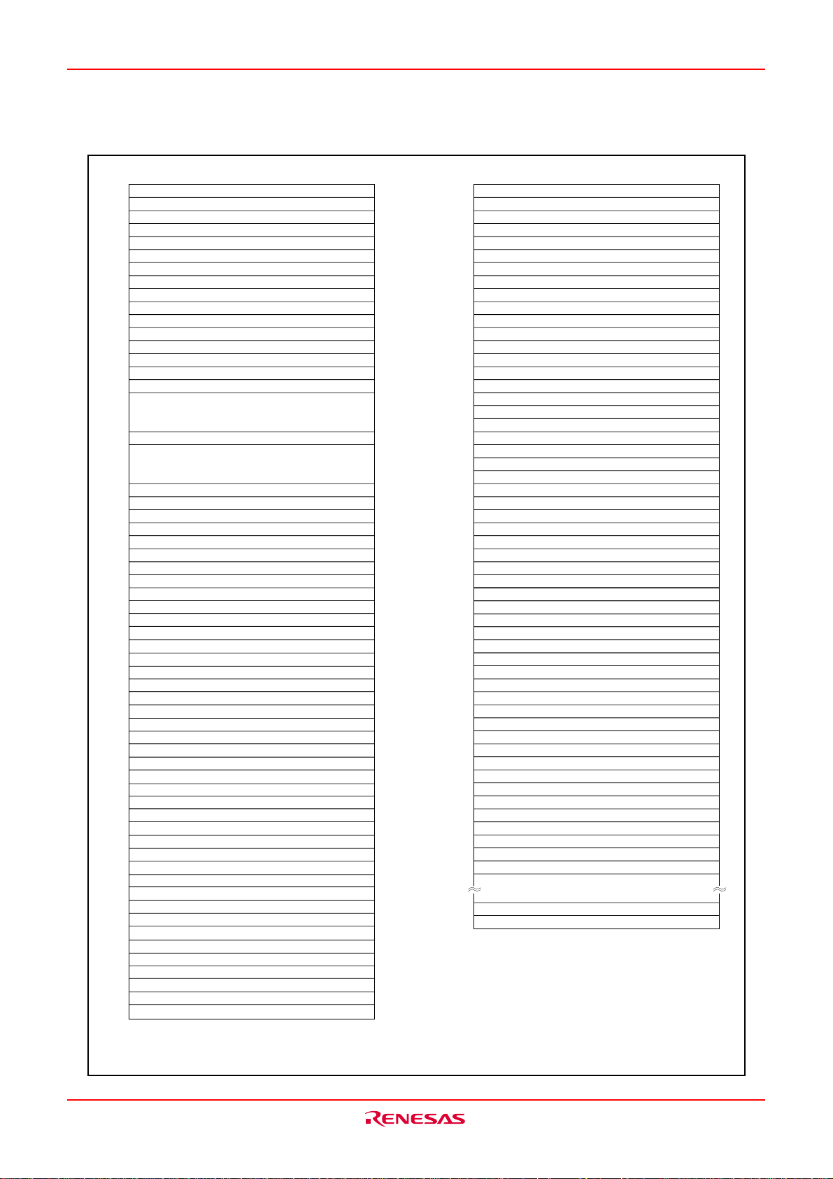
Note 1: The areas that nothing are allocated in SFR are reserved. Read and Write to the areas are inhibited.
Fig.CA-2 Location of peripheral unit control registers (1)
Rev.1.00 Jul 16, 2004 page 22 of 266
REJ03B0100-0100Z
Page 23
M16C/6KA Group SFR
0280
16
0281
16
0282
16
0283
16
0284
16
0285
16
0286
16
0287
16
0288
16
0289
16
028A
16
028B
16
028C
16
028D
16
028E
16
028F
16
0290
16
0291
16
0292
16
0293
16
0294
16
0295
16
0296
16
0297
16
0298
16
0299
16
029A
16
029B
16
029C
16
029D
16
029E
16
029F
16
PS20 shift
02A0
16
PS20 status
02A1
16
PS20 control register (PS20CON)
02A2
16
02A3
16
PS21 shift
02A4
16
PS21 status
02A5
16
PS21 control register (PS21CON)
02A6
16
02A7
16
PS22 shift
02A8
16
PS22 status
02A9
16
PS22 control register (PS22CON)
02AA
16
02AB
16
PS2 mode register (PS2MOD)
02AC
16
02AD
16
02AE
16
02AF
16
Serial Interrupt control register 0 (SERCON0)
02B0
16
Serial Interrupt control register 1 (SERCON1)
02B1
16
IRQ request register 0 (IRQ0)
02B2
16
IRQ request register 1 (IRQ1)
02B3
16
IRQ request register 2 (IRQ2)
02B4
16
IRQ request register 3 (IRQ3)
02B5
16
IRQ request register 4 (IRQ4)
02B6
16
Serial Interrupt control register 2 (SERCON2)
02B7
16
02B8
16
02B9
16
02BA
16
02BB
16
02BC
16
02BD
16
02BE
16
02BF
16
register
register
register
register
register
register
(PS20SR)
(PS21SR)
(PS22SR)
(PS20STS)
(PS21STS)
(PS22STS)
02C0
16
Data bus buffer register0 (DBB0)
02C1
16
Data bus buffer status register0 (DBBSTS0)
02C2
16
Data bus buffer register1 (DBB1)
02C3
16
Data bus buffer status register1 (DBBSTS1)
02C4
16
Data bus buffer register2 (DBB2)
02C5
16
Data bus buffer status register2 (DBBSTS2)
02C6
16
Data bus buffer register3 (DBB3)
02C7
16
Data bus buffer status register3 (DBBSTS3)
02C8
16
02C9
16
Data bus buffer control register1 (DBBCON1)
Gate A20 control register (GA20CON)
02CA
16
02CB
16
02CC
16
02CD
16
02CE
16
02CF
16
LPC1 address registerL (LPC1ADL)
02D0
16
02D1
16
LPC1 address registerH (LPC1ADH)
LPC2 address registerL (LPC2ADL)
02D2
16
LPC2 address registerH (LPC2ADH)
02D3
16
LPC3 address registerL (LPC3ADL)
02D4
16
LPC3 address registerH (LPC3ADH)
02D5
16
LPC control register (LPCCON)
02D6
16
02D7
16
02D8
16
02D9
16
02DA
16
02DB
16
02DC
16
02DD
16
02DE
16
02DF
16
02E0
16
Port P11 (P11)
02E1
16
Port P12 (P12)
02E2
16
Port P11 direction register (PD11)
02E3
16
Port P12 direction register (PD12)
02E4
16
Port P13 (P13)
02E5
16
Port P14 (P14)
Port P13 direction register (PD13)
02E6
16
Port P14 direction register (PD14)
02E7
16
02E8
16
Port P15 (P15)
02E9
16
Port P16 (P16)
Port P15 direction register (PD15)
02EA
16
02EB
16
Port P16 direction register (PD16)
02EC
16
02ED
16
02EE
16
02EF
16
02F0
16
Port function selection register 2 (PSL2)
02F1
16
02F2
16
Pull-up resistor control register 5 (PUR5)
02F3
16
Pull-up resistor control register 6 (PUR6)
Key input interrupt 1 enable register (KIN1EN)
02F4
16
Key input interrupt 1 edge selection regiter (KINSEL)
02F5
16
P14 event register (P14EV)
02F6
16
Port control register3 (PCR3)
02F7
16
Port function selection register0 (PSL0)
02F8
16
Port function selection register1 (PSL1)
02F9
16
Port P4 input register (P4PIN)
02FA
16
02FB
16
Port P7 input register (P7PIN)
02FC
16
Pull-up control register3 (PUR3)
Pull-up control register4 (PUR4)
02FD
16
Port control register1 (PCR1)
02FE
16
Port control register2 (PCR2)
02FF
16
Note 1: The areas that nothing are allocated in SFR are reserved. Read and Write to the areas are inhibited.
Fig.CA-3 Location of peripheral unit control registers (2)
Rev.1.00 Jul 16, 2004 page 23 of 266
REJ03B0100-0100Z
Page 24
M16C/6KA Group SFR
030016
PWM0 prescaler (PREPWM0)
030116
PWM0 register (PWM0)
030216
PWM1 prescaler (PREPWM1)
030316
PWM1 register (PWM1)
PWM2 prescaler (PREPWM2)
030416
030516
PWM2 register (PWM2)
030616
PWM3 prescaler (PREPWM3)
030716
PWM3 register (PWM3)
030816
PWM4 prescaler (PREPWM4)
030916
PWM4 register (PWM4)
030A16
PWM5 prescaler (PREPWM5)
030B16
PWM5 register (PWM5)
030C16
PWM control register 0 (PWMCON0)
030D16
PWM control register 1 (PWMCON1)
030E16
030F16
031016
031116
031216
031316
031416
031516
031616
031716
031816
031916
031A16
031B16
031C16
031D16
031E16
031F16
032016
032116
032216
032316
032416
032516
032616
032716
032816
032916
032A16
032B16
032C16
032D16
032E16
032F16
033016
033116
033216
033316
033416
033516
033616
033716
033816
033916
033A16
033B16
033C16
033D16
033E16
033F16
2
I
C2 data shift register (S02)
2
C2 address register (S0D2)
I
2
C2 control register 0 (S1D2)
I
2
I
C2 clock control register (S22)
2
I
C2 start/stop condition control register (S2D2)
2
C2 control register 1 (S3D2)
I
2
I
C2 control register 2 (S4D2)
2
C2 status register (S12)
I
2
C
0 data
I
2
I
2
I
2
I
2
I
2
I
2
I
2
I
2
I
2
I
2
I
2
I
2
I
2
I
2
I
2
I
shift register (S00)
C0 address register (S0D0)
C0 control register0 (S1D0)
C0 clock control register (S20)
C0 start/stop condition control register (S2D0)
C0 control register1 (S3D0)
C0 control register2 (S4D0)
C0 status register (S10)
C
1 data
shift register (S01)
C1 address register (S0D1)
C1 control register0 (S1D1)
C1 clock control register (S21)
C1 start/stop condition control register (S2D1)
C1 control register1 (S3D1)
C1 control register2 (S4D1)
C1 status register (S11)
034016
TimerB3,4,5 count start flag (TBSR)
034116
034216
034316
034416
034516
034616
034716
034816
034916
034A16
034B16
034C16
034D16
034E16
034F16
035016
TimerB3 register (TB3)
035116
035216
TimerB4 register (TB4)
035316
035416
TimerB5 register (TB5)
035516
035616
035716
035816
035916
035A16
TimerB3 mode register (TB3MR)
035B16
TimerB4 mode register (TB4MR)
035C16
TimerB5 mode register (TB5MR)
035D16
Interrupt event select register 1 (IFSR1)
035E16
035F16
Interrupt event select register 0 (IFSR0)
036016
SI/O3 transmit/receive register (S3TRR)
036116
036216
SI/O3 control register (S3C)
036316
SI/O3 communication speed register (S3BRG)
036416
SI/O4 transmit/receive register (S4TRR)
036516
036616
SI/O4 control register (S4C)
036716
SI/O4 communication speed register (S4BRG)
036816
036916
036A16
036B16
036C16
036D16
036E16
036F16
037016
037116
037216
037316
037416
037516
037616
037716
037816
037916
037A16
037B16
037C16
037D16
037E16
037F16
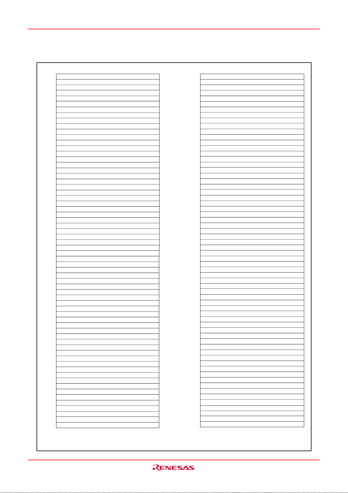
Note 1: The areas that nothing are allocated in SFR are reserved. Read and Write to the areas are inhibited.
Fig.CA-4 Location of peripheral unit control registers (3)
Rev.1.00 Jul 16, 2004 page 24 of 266
REJ03B0100-0100Z
Page 25
M16C/6KA Group SFR
03C0
0380
16
Count start flag
0381
16
One-shot start flag
0382
16
Trigger select register
0383
16
Up-down flag
0384
16
0385
16
0386
16
TimerA0
0387
16
0388
16
TimerA1
0389
16
038A
16
TimerA2
038B
16
038C
16
TimerA3
038D
16
038E
16
TimerA4
038F
16
0390
16
TimerB0
0391
16
0392
16
TimerB1
0393
16
0394
16
TimerB2
0395
16
TimerA0 mode register
0396
16
TimerA1 mode register
0397
16
TimerA2 mode register
0398
16
0399
16
TimerA3 mode register
TimerA4 mode register
039A
16
TimerB0 mode register
039B
16
TimerB1 mode register
039C
16
TimerB2 mode register
039D
16
039E
16
039F
16
03A0
16
03A1
16
03A2
16
03A3
16
03A4
16
03A5
16
03A6
16
03A7
16
UART1 transmit/receive mode register (U1MR)
03A8
16
UART1 communication speed register (U1BRG)
03A9
16
03AA
16
UART1 tranmit buffer register (U1TB)
03AB
16
UART1 transmit/receive control register0 (U1C0)
03AC
16
UART1 transmit/receive control register1 (U1C1)
03AD
16
03AE
16
UART1 receive buffer register (U1RB)
03AF
16
UART transmit/receive control register2 (UCON)
03B0
16
03B1
16
03B2
16
03B3
16
Flash memory identification register (FTR)
03B4
16
Flash memory control register1 (FMR1)
03B5
16
03B6
16
Flash memory control register0 (FMR0)
03B7
16
03B8
16
03B9
16
03BA
16
03BB
16
03BC
16
03BD
16
03BE
16
03BF
16
(TA0)
(TA1)
(TA2)
(TA3)
(TA4)
(TB0)
(TB1)
(TB2)
(TABSR)
(UDF)
(ONSF)
(TRGSR)
(TA0MR)
(TA1MR)
(TA2MR)
(TA3MR)
(TA4MR)
(TB0MR)
(TB1MR)
(TB2MR)
Note 1: The areas that nothing are allocated in SFR are reserved. Read and Write to the areas are inhibited.
16
A-D register0 (AD0)
03C1
16
03C2
16
A-D register1 (AD1)
03C3
16
03C4
16
A-D register2 (AD2)
03C5
16
03C6
16
A-D register3 (AD3)
03C7
16
03C8
16
A-D register4 (AD4)
03C9
16
03CA
16
A-D register5 (AD5)
03CB
16
03CC
16
A-D register6 (AD6)
03CD
16
03CE
16
A-D register7 (AD7)
03CF
16
03D0
16
03D1
16
03D2
16
03D3
16
A-D control register2 (ADCON2)
03D4
16
03D5
16
03D6
16
A-D control register0 (ADCON0)
03D7
16
A-D control register1 (ADCON1)
03D8
16
03D9
16
03DA
16
03DB
16
03DC
16
03DD
16
03DE
16
03DF
16
03E0
16
Port P0 (P0)
03E1
16
Port P1 (P1)
Port P0 direction register (P0D)
03E2
16
03E3
16
Port P1 direction register (P1D)
03E4
16
Port P2 (P2)
03E5
16
Port P3 (P3)
Port P2 direction register (P2D)
03E6
16
03E7
16
Port P3 direction register (P3D)
03E8
16
Port P4 (P4)
Port P5 (P5)
03E9
16
Port P4 direction register (P4D)
03EA
16
Port P5 direction register (P5D)
03EB
16
03EC
16
Port P6 (P6)
Port P7 (P7)
03ED
16
Port P6 direction register (P6D)
03EE
16
Port P7 direction register (P7D)
03EF
16
Port P8 (P8)
03F0
16
Port P9 (P9)
03F1
16
Port P8 direction register (P8D)
03F2
16
Port P9 direction register (P9D)
03F3
16
Port P10 (P10)
03F4
16
03F5
16
Port P10 direction register (P10D)
03F6
16
03F7
16
03F8
16
03F9
16
03FA
16
03FB
16
03FC
16
Pull-up control register0 (PUR0)
Pull-up control register1 (PUR1)
03FD
16
Pull-up control register2 (PUR2)
03FE
16
Port control register0 (PCR0)
03FF
16
Fig.CA-5 Location of peripheral unit control registers (4)
Rev.1.00 Jul 16, 2004 page 25 of 266
REJ03B0100-0100Z
Page 26
M16C/6KA Group
Software Reset
Software Reset
Writing “1” to bit 3 of the processor mode register 0 (address 000416) applies a (software) reset to the
microcomputer. A software reset has almost the same effect as a hardware reset. The contents of internal
RAM are retained.
Processor Mode
(1) Types of Processor Mode
The single-chip mode is supported in processor mode.
• Single-chip mode
In single-chip mode, only internal memory space (SFR, internal RAM, and internal ROM) can be accessed.
Ports P0 to P16 can be used as programmable I/O ports or as I/O ports for the internal peripheral functions.
Fig. BG-1 shows the structure of processor mode register 0 and processor mode register 1.
Processor mode register 0 (Note 1)
b7 b6 b5 b4 b3 b2 b1 b0
00000
Symbol Address When reset
PM0 0004
PM00
PM01
Reserved bit Must always be set to “0”
PM03
Reserved bit Must always be set to “0”
Note 1: Set bit 1 of the protect register (address 000A16) to “1” when writing new
values to this register.
Processor mode register 1 (Note 1)
b7 b6 b5 b4 b3 b2 b1 b0
00
00
Symbol Address When reset
PM1 0005
0
Reserved bit
Nothing is assigned.
In an attempt to write to these bits, write “0”. The value, if read, turns out
to be indeterminate.
16
Bit name FunctionBit symbol
Processor mode bit
Software reset bit
16
Bit name FunctionBit symbol
00
16
(Note 2)
b1 b0
0 0: Single-chip mode
0 1: Inhibited
1 0: Inhibited
1 1: Inhibited
The device is reset when this bit is set
to “1”. The value of this bit is “0” when
read.
00000XX0
2
Must always be set to “0”
WR
WR
Reserved bit
PM17 Wait bit
Note 1: Set bit 1 of the protect register (address 000A
Fig.BG-1 Processor mode register 0 and 1
Rev.1.00 Jul 16, 2004 page 26 of 266
REJ03B0100-0100Z
values to this register.
Must always be set to “0”
0 : No wait state
1 : Wait state inserted
16
) to “1” when writing new
Page 27
M16C/6KA Group
Bus control
Bus control
(1) Software wait
A software wait can be inserted by setting the wait bit (bit 7) of the processor mode register 1 (address
000516) (Note) .
A software wait is inserted in the internal ROM/RAM area by setting the wait bit of the processor mode
register 1. When set to “0”, each bus cycle is executed in one BCLK cycle. When set to “1”, each bus cycle
is executed in 2 BCLK cycles. After the microcomputer has been reset, this bit defaults to “0”.
Set this bit after referring to the recommended operating conditions (main clock input oscillation frequency)
of the electric characteristics.
The SFR area is always accessed in two BCLK cycles regardless of the setting of these control bits.
Table.EF-1 shows the software wait and bus cycles. Fig.EF-1 shows example bus timing when using software waits.
Note: Before attempting to change the contents of the processor mode register 1, set bit 1 of the protect
register (address 000A16) to “1”.
Table.EF-1 Software waits and bus cycles
Area Wait bit
SFR
Internal
ROM/RAM
Invalid 2 BCLK cycles
0 1 BCLK cycle
1 2 BCLK cycles
Bus cycle
Rev.1.00 Jul 16, 2004 page 27 of 266
REJ03B0100-0100Z
Page 28
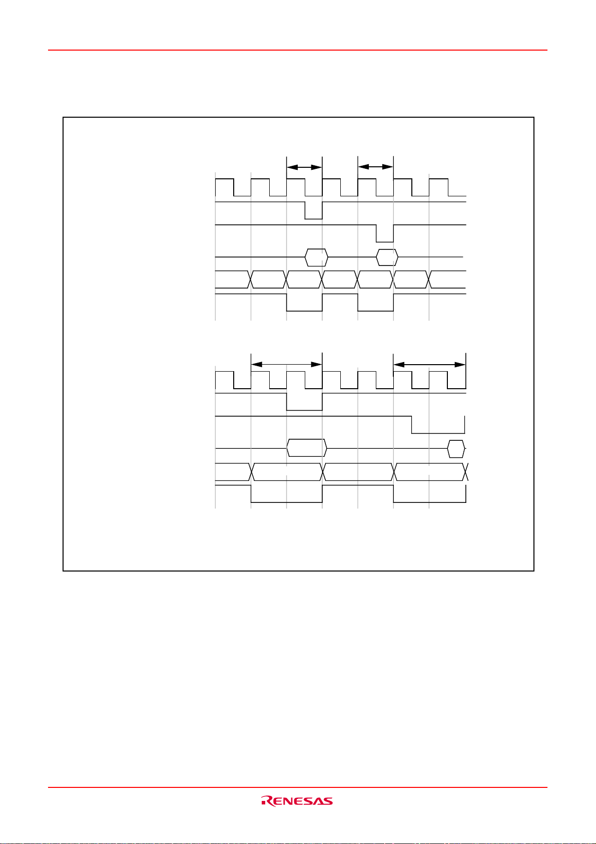
M16C/6KA Group
Bus control
No wait
With wait
BCLK
Write signal
Read signal
Data bus
Address bus
Chip select
BCLK
Write signal
Read signal
Bus cycle
(Note 1)
Address
Bus cycle
(Note 1)
Output
Bus cycle
(Note 1)
Input
Address
Bus cycle
(Note 1)
Data bus
Address bus
Address
Chip select
Note 1: This timing sample shows the lenth of bus cycle. It is possible that the read cyles, write cycle
comes after this cycle in succession.
Fig.EF-1 Typical bus timings using software wait
Output
Input
Address
Rev.1.00 Jul 16, 2004 page 28 of 266
REJ03B0100-0100Z
Page 29
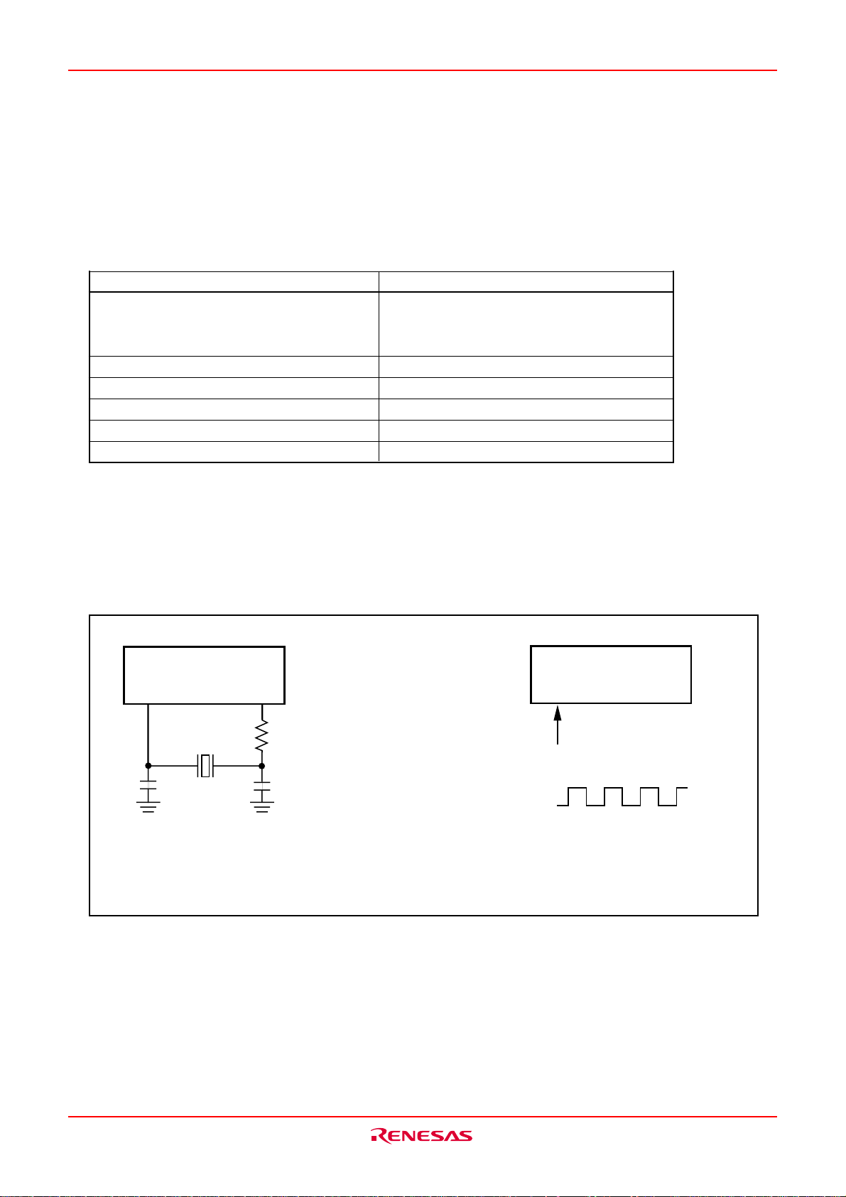
M16C/6KA Group
Clock Generating Circuit
Clock Generating Circuit
The clock generating circuit contains two oscillator circuits that supply the operating clock sources to the
CPU and internal peripheral units.
Table.WA-1 Main clock generating circuits
Main clock generating circuit
Use of clock • CPU’s operating clock source
• Internal peripheral units’
operating clock source
Usable oscillator Ceramic oscillator
Pins to connect oscillator XIN, XOUT
Oscillation stop/restart function Available
Oscillator status immediately after reset Oscillating
Other Externally derived clock can be input
Example of oscillator circuit
Fig.WA-1 shows some examples of the main clock circuit, one using an oscillator connected to the circuit,
and the other one using an externally derived clock for input. Circuit constants in Fig.WA-1 vary with oscillator used. Use the values recommended by the manufacturer of your oscillator.
Microcomputer
(Built-in feedback resistor)
X
IN
C
IN
Note: Insert a damping resistor if required. The resistance will vary depending on the oscillator and the oscillation drive
capacity setting. Use the value recommended by the maker of the oscillator.
When the oscillation drive capacity is set to low, check that oscillation is stable.
Apply the feedback register between X
X
OUT
(Note)
R
d
C
OUT
IN
and X
OUT
if required by oscillator maker.
Fig.WA-1 Examples of main clock
Microcomputer
(Built-in feedback resistor)
X
IN
Externally derived clock
Vcc
Vss
X
OUT
Open
Rev.1.00 Jul 16, 2004 page 29 of 266
REJ03B0100-0100Z
Page 30
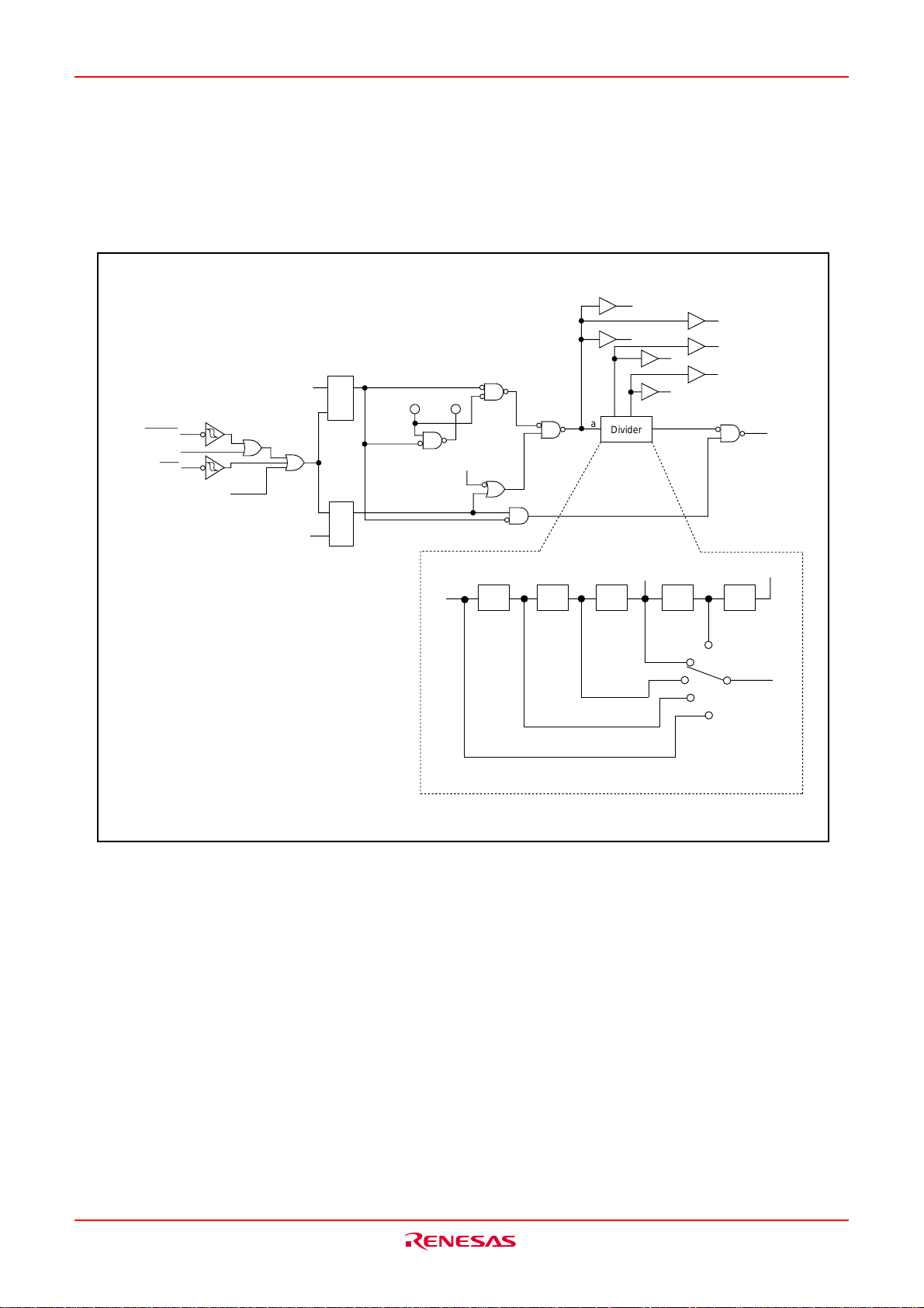
M16C/6KA Group
Clock Generating Circuit
Clock Control
Fig.WA-2 shows the block diagram of the clock generating circuit.
RESET
Software reset
NMI
Interrupt request
level judgment
output
CM10 “1”
Write signal
WAIT instruction
Q
S
R
QS
R
X
IN
Main clock
X
OUT
CM02
f
1
f
AD
f
8
f
32
c
b
Divider
d
a
f1SIO2
f8SIO2
f32SIO2
BCLK
CM0i : Bit i at address 0006
CM1i : Bit i at address 0007
Fig.WA-2 Clock generating circuit
b
a
16
16
1/2 1/2 1/2 1/2
CM06=0
CM17,CM16=10
CM06=0
CM17,CM16=01
CM06=0
CM17,CM16=00
CM06=1
CM06=0
CM17,CM16=11
Details of divider
c
1/2
d
Rev.1.00 Jul 16, 2004 page 30 of 266
REJ03B0100-0100Z
Page 31

M16C/6KA Group
The following paragraphs describes the clocks generated by the clock generating circuit.
Clock Generating Circuit
(1) Main clock
The main clock is generated by the main clock oscillation circuit. After a reset, the clock is divided by 8 to
the BCLK. The clock can be stopped using the main clock stop bit (bit 5 at address 000616).
After the oscillation of the main clock oscillation circuit has stabilized, the drive capacity of the main clock
oscillation circuit can be reduced using the XIN-XOUT drive capacity select bit (bit 5 at address 000716).
Reducing the drive capacity of the main clock oscillation circuit reduces the power dissipation. This bit defaults to “1” when shifting from high speed mode or mid-speed mode to stop mode and after a reset.
(2) BCLK
The BCLK is the clock that drives the CPU, and is either the main clock or is derived by dividing the main
clock by 2, 4, 8, or 16. The BCLK is derived by dividing the main clock by 8 after a reset.
When shifting from high speed mode or mid-speed mode to stop mode, the main clock division select bit (bit
6 at 000616) is set to “1”.
(3) Peripheral function clock
f1, f8, f32, f1SIO2, f8SIO2, f32SIO2, fAD
The clock for the peripheral devices is derived from the main clock or by dividing it by 8 or 32. The peripheral
function clock is stopped by stopping the main clock or by setting the WAIT peripheral function clock stop bit
(bit 2 at 000616) to “1” and then executing a WAIT instruction.
Rev.1.00 Jul 16, 2004 page 31 of 266
REJ03B0100-0100Z
Page 32

M16C/6KA Group
Clock Generating Circuit
Fig.WA-3 shows the system clock control registers 0 and 1.
System clock control register 0
b7 b6 b5 b4 b3 b2 b1 b0
0
001
(Note 1)
Symbol Address When reset
CM0 0006
16 4816
Bit name FunctionBit symbol WR
CM00
CM01
CM02
Reserved bit
Reserved bit
CM06
Reserved bit
Clock output function
select bit
WAIT peripheral function
clock stop bit
Main clock division select
bit 0 (Note 2)
b1 b0
0 0 : I/O port P5
0 1 : Inhibited
1 0 : f
8
output
1 1 : f
32
0 :Do not stop peripheral clock in wait mode
1 :Stop peripheral clock in wait mode
Always set to
Always set to
0 : CM16 and CM17 valid
1 : Division by 8 mode
Always set to
7
output
“1”
“0”
“0”
Note 1 : Set bit 0 of the protect register (address 000A16) to "1" before writing to this register.
Note 2 : The bit is set to "1" when shifting from high speed mode or mid speed mode to stop mode and
after reset.
System clock control register 1
b7 b6 b5 b4 b3 b2 b1 b0
00
00
(Note 1)
Symbol Address When reset
CM1 0007
16 2016
Bit name FunctionBit symbol WR
CM10
Reserved bit
Reserved bit
Reserved bit
Reserved bit
CM15
CM16
CM17
All clock stop control bit
(Note 4)
IN-XOUT
X
select bit (Note 2)
Main clock division
select bit 1 (Note 3)
drive capacity
Note 1: Set bit 0 of the protect register (address 000A16) to "1"
Note 2: The bit is set to "1" when shifting from high speed mode or mid speed mode to stop mode and
after reset.
Note 3: Can be selected when bit 6 of the system clock control register 0 (address 0006
If
"1"
, division mode is fixed at 8.
Note 4: If this bit is set to "1", XOUT turns "H", and the built-in feedback resistor turns null.
Fig.WA-3 System clock control registers 0 and 1
0 : Clock on
1 : All clocks off (stop mode)
Always set to
Always set to
Always set to
Always set to
0 : LOW
1 : HIGH
b7 b6
0 0 : No division mode
0 1 : Division by 2 mode
1 0 : Division by 4 mode
1 1 : Division by 16 mode
before writing to this register.
“0”
“0”
“0”
“0”
16) is
"0".
Rev.1.00 Jul 16, 2004 page 32 of 266
REJ03B0100-0100Z
Page 33

M16C/6KA Group
Clock Generating Circuit
Clock Output
In single-chip mode, the clock output function select bits (bits 0 and 1 at address 000616) enable f8, f32 to be
output from the P57/CLKOUT pin. When the WAIT peripheral function clock stop bit (bit 2 at address 000616)
is set to “1”, the output of f8 and f32 stops when a WAIT instruction is executed.
By setting the f1 output function selection bits (bits 0 and 1 at address 02F116), the same frequency clock
with f(XIN) can be output from P110 and P111.
Stop Mode
Writing “1” to the all-clock stop control bit (bit 0 at address 000716) stops all oscillation and the microcomputer enters stop mode. In stop mode, the content of the internal RAM is retained provided that VCC remains
above 2V.
The oscillation , BCLK, f1 to f32, f1SIO2 to f32SIO2, and fAD stop in stop mode, peripheral functions such as the
A-D converter and watchdog timer do not function. However, timer A and timer B operate provided that the
event counter mode is set to an external pulse, and UART1, SIO3,4 functions provided an external clock is
selected. Table.WA-2 shows the status of the ports in stop mode.
Stop mode is cancelled by a hardware reset or interrupt. If an interrupt is to be used to cancel stop mode, that
interrupt must first have been enabled. After the restoration by interrupt, the corresponding interrupt routine
will be processed. When shifting from high speed mode or mid-speed mode to stop mode, the main clock
division select bit 0 (bit 6 at 000616) is set to “1”.
Table.WA-2 Port status during stop mode
Pin Single-chip mode
Port
CLKOUT When f8, f32 selected
Retains status before stop mode
Retains status before stop mode
Rev.1.00 Jul 16, 2004 page 33 of 266
REJ03B0100-0100Z
Page 34

M16C/6KA Group
Wait Mode
Wait Mode
When a WAIT instruction is executed, the BCLK stops and the microcomputer enters the wait mode. In this
mode, oscillation continues but the BCLK and watchdog timer stop. Writing “1” to the WAIT peripheral function clock stop bit and executing a WAIT instruction stops the clock being supplied to the internal peripheral
functions, allowing power dissipation to be reduced. Table.WA-3 shows the status of the ports in wait mode.
Wait mode is cancelled by a hardware reset or interrupt. If an interrupt is used to cancel wait mode, the
microcomputer restarts from interrupt routine using as BCLK, the clock that had been selected when the
WAIT instruction was executed.
Table.WA-3 Port status during wait mode
Pin Single-chip mode
CLKOUT When f8, f32 selected Does not stop when the WAIT peripheral function clock stop
bit is “0”.
When the WAIT peripheral function clock stop bit is “1”, the
status immediately prior to entering wait mode is maintained.
Port maintained the status immediately prior to entering wait mode
Rev.1.00 Jul 16, 2004 page 34 of 266
REJ03B0100-0100Z
Page 35

M16C/6KA Group
Status Transition Of BCLK
Status Transition Of BCLK
Power dissipation can be reduced and low-voltage operation achieved by changing the count source for
BCLK. Table.WA-4 shows the operating modes corresponding to the settings of system clock control registers 0 and 1.
After a reset, operation defaults to division by 8 mode. When shifting from high speed mode or mid-speed
mode to stop mode, and after a reset main clock division select bit 0 (bit 6 at address 000616) is set to “1”.
(1) Division by 2 mode
The main clock is divided by 2 to obtain the BCLK.
(2) Division by 4 mode
The main clock is divided by 4 to obtain the BCLK.
(3) Division by 8 mode
The main clock is divided by 8 to obtain the BCLK. After reset, it works in this mode. Note that oscillation of
the main clock must have stabilized before transferring from this mode to No-division, Division by 2 and
Division by 4 mode.
(4) Division by 16 mode
The main clock is divided by 16 to obtain the BCLK.
(5) No-division mode
The main clock is used as the BCLK.
Table.WA-4 Operating modes dictated by settings of system clock control registers 0 and 1
CM17 CM16 CM06
0 1 0 Division by 2 mode
1 0 0 Division by 4 mode
Invalid Invalid 1 Division by 8 mode
1 1 0 Division by 16 mode
0 0 0 No-division mode
Operating mode of BCLK
Rev.1.00 Jul 16, 2004 page 35 of 266
REJ03B0100-0100Z
Page 36

M16C/6KA Group
Power control
Power control
The following is a description of the power control modes:
Modes
Power control is available in three modes.
(1) Normal operation mode
• High-speed mode
Divide-by-1 frequency of the main clock becomes the BCLK. The CPU operates with the internal clock
selected. Each peripheral function operates according to its assigned clock.
• Medium-speed mode
Divide-by-2, divide-by-4, divide-by-8, or divide-by-16 frequency of the main clock becomes the BCLK. The
CPU operates according to the internal clock selected. Each peripheral function operates according to its
assigned clock.
(2) Wait mode
The CPU operation is stopped. The oscillators do not stop.
(3) Stop mode
All oscillators stop. The CPU and all built-in peripheral functions stop. This mode, among the three modes
listed here, is the most effective in decreasing power consumption.
Fig.WA-4 is the state transition diagram of (1) to (3).
Transition of stop mode, wait mode
Reset
All oscillators stop
Stop mode
All oscillators stop
Stop mode
CM10 = “1”
Interrupt
Interrupt
CM10 = “1”
Medium-speed mode
(Divided-by-8 mode)
High-speed/medium-
speed mode
WAIT
command
Interrupt
WAIT
command
Interrupt
CPU operation stop
Wait mode
CPU operation stop
Wait mode
Normal mode
Fig.WA-4 State transition diagram of Power control mode
Rev.1.00 Jul 16, 2004 page 36 of 266
REJ03B0100-0100Z
Page 37

M16C/6KA Group
Protection
Protection
The protection function is provided so that the values in important registers cannot be changed in the event
that the program runs out of control. Fig.WA-5 shows the protect register. The values in the processor mode
register 0 (address 000416), processor mode register 1 (address 000516), system clock control register 0
(address 000616), system clock control register 1 (address 000716), can only be changed when the respective bit in the protect register is set to “1”.
Protect register
b7 b6 b5 b4 b3 b2 b1 b0
0
Symbol Address When reset
16
PRCR 000A
XXXXX000
2
Fig.WA-5 Protect register
Bit nameBit symbol
Enables writing to system clock
PRC0
PRC1
Reserved bit
Nothing is assigned.
In an attempt to write to these bits, write “0”. The value, if read, turns out to be
indeterminate.
control registers 0 and 1 (addresses
0006
16
and 0007
Enables writing to processor mode
registers 0 and 1 (addresses 0004
and 0005
16
)
16
)
0 : Write-inhibited
1 : Write-enabled
0 : Write-inhibited
16
1 : Write-enabled
Must be "0"
Function
WR
Rev.1.00 Jul 16, 2004 page 37 of 266
REJ03B0100-0100Z
Page 38

M16C/6KA Group
Interrupt
Overview of Interrupt
Type of Interrupts
Fig.DD-1 lists the types of interrupts.
Software
Interrupt
Hardware
Special
Peripheral I/O (Note)
Undefined instruction (UND instruction)
Overflow (INTO instruction)
BRK instruction
INT instruction
Reset
_______
NMI
________
DBC
Watchdog timer
Single step
Address matched
Note: Peripheral I/O interrupts are generated by the peripheral functions built into the microcomputer system.
Fig.DD-1 Classification of interrupts
• Maskable interrupt : An interrupt which can be enabled (disabled) by the interrupt enable flag
(I flag) or whose interrupt priority can be changed by priority level.
• Non-maskable interrupt : An interrupt which cannot be enabled (disabled) by the interrupt enable flag
(I flag) or whose interrupt priority cannot be changed by priority level.
Rev.1.00 Jul 16, 2004 page 38 of 266
REJ03B0100-0100Z
Page 39

M16C/6KA Group
Interrupt
Software Interrupts
A software interrupt occurs when executing certain instructions. Software interrupts are non-maskable interrupts.
• Undefined instruction interrupt
An undefined instruction interrupt occurs when executing the UND instruction.
• Overflow interrupt
An overflow interrupt occurs when executing the INTO instruction with the overflow flag (O flag) set to “1”.
The following are instructions whose O flag changes by arithmetic:
ABS, ADC, ADCF, ADD, CMP, DIV, DIVU, DIVX, NEG, RMPA, SBB, SHA, SUB
• BRK interrupt
A BRK interrupt occurs when executing the BRK instruction.
• INT interrupt
An INT interrupt occurs when assigning one of software interrupt numbers 0 through 63 and executing the
INT instruction. Software interrupt numbers 0 through 52 are assigned to peripheral I/O interrupts, so executing the INT instruction allows executing the same interrupt routine that a peripheral I/O interrupt does.
The stack pointer (SP) used for the INT interrupt is dependent on which software interrupt number is involved.
So far as software interrupt numbers 0 through 31 are concerned, the microcomputer saves the stack pointer
assignment flag (U flag) when it accepts an interrupt request. If change the U flag to “0” and select the
interrupt stack pointer (ISP), and then execute an interrupt sequence. When returning from the interrupt
routine, the U flag is returned to the state it was before the acceptance of interrupt request. So far as
software numbers 32 through 63 are concerned, the stack pointer does not make a shift.
Rev.1.00 Jul 16, 2004 page 39 of 266
REJ03B0100-0100Z
Page 40

M16C/6KA Group
Interrupt
Hardware Interrupts
Hardware interrupts are classified into two types — special interrupts and peripheral I/O interrupts.
(1) Special interrupts
Special interrupts are non-maskable interrupts.
• Reset
Reset occurs if an “L” is input to the RESET pin.
_______
• NMI interrupt
_______ _______
An NMI interrupt occurs if an “L” is input to the NMI pin.
________
• DBC interrupt
This interrupt is exclusively for the debugger, do not use it in other circumstances.
• Watchdog timer interrupt
Generated by the watchdog timer.
• Single-step interrupt
This interrupt is exclusively for the debugger, do not use it in other circumstances. With the debug flag (D
flag) set to “1”, a single-step interrupt occurs after one instruction is executed.
• Address match interrupt
An address match interrupt occurs immediately before the instruction held in the address indicated by the
address match interrupt register is executed with the address match interrupt enable bit set to “1”.
If an address other than the first address of the instruction in the address match interrupt register is set, no
address match interrupt occurs.
____________
(2) Peripheral I/O interrupts
A peripheral I/O interrupt is generated by one of built-in peripheral functions. Built-in peripheral functions are
dependent on classes of products, so the interrupt factors are also dependent on classes of products. The
interrupt vector table is the same as the one for software interrupt numbers 0 through 52 the INT instruction
uses. Peripheral I/O interrupts are maskable interrupts.
1)Key-input interrupt 0
___
A key-input interrupt occurs if an “L” is input to the KI pin.
2)Key-input interrupt 1
___
A key-input interrupt occurs if an “L” or “H” is input to the KI pin.
3)A-D conversion interrupt
This is an interrupt that the A-D converter generates.
4)UART1, SI/O3 and SI/O4 transmission interrupt
These are interrupts that the serial I/O transmission generates.
5)UART1, SI/O3 and SI/O4 reception interrupt
These are interrupts that the serial I/O reception generates.
6)Timer A0 interrupt through timer A4 interrupt
These are interrupts that timer A generates
7)Timer B0 interrupt through timer B5 interrupt
These are interrupts that timer B generates.
Rev.1.00 Jul 16, 2004 page 40 of 266
REJ03B0100-0100Z
Page 41

M16C/6KA Group
________ __________
8)INT0 interrupt through INT11 interrupt
______ ______
Interrupt
An INT interrupt occurs if either a rising edge or a falling edge or both edges are input to the INT pin.
9)IBF0 to IBF3, OBE interrupt
These are interrupts that host bus interface generates.
______________
10) LRESET interrupt
______________ ______________
LRESET interrupt occurs if an “L” is input to LRESET pin.
11)I2C0, I2C1, I2C2, SCL0, SDA0, SCL1, SDA1, SCL2, SDA2 interrupt
These are interrupts that I2C bus interface generates.
12)PS20 to PS22 interrupt
These are interrupt that PS2 interface generates.
Rev.1.00 Jul 16, 2004 page 41 of 266
REJ03B0100-0100Z
Page 42

M16C/6KA Group
Interrupt
Interrupts and Interrupt Vector Tables
If an interrupt request is accepted, a program branches to the interrupt routine set in the interrupt vector
table. Set the first address of the interrupt routine in each vector table. Fig.DD-2 shows the format for
specifying the address.
Two types of interrupt vector tables are available — fixed vector table in which addresses are fixed and
variable vector table in which addresses can be varied by the setting.
LSB
Vector address + 0
MSB
Low address
Mid address
Vector address + 1
0 0 0 0 High address
Vector address + 2
Fig.DD-2 Format for specifying interrupt vector addresses
• Fixed vector tables
The fixed vector table is a table in which addresses are fixed. The vector tables are located in an area
extending from FFFDC16 to FFFFF16. One vector table comprises four bytes. Set the first address of
interrupt routine in each vector table. Table.DD-1 shows the interrupts assigned to the fixed vector tables
and addresses of vector tables.
Table.DD-1 Interrupts assigned to the fixed vector tables and addresses of vector tables
Interrupt source Vector table addresses Remarks
Address (L) to address (H)
Undefined instruction FFFDC16 to FFFDF16 Interrupt on UND instruction
Overflow FFFE016 to FFFE316 Interrupt on INTO instruction
BRK instruction FFFE416 to FFFE716
Address match FFFE816 to FFFEB16 There is an address-matching interrupt enable bit
Single step (Note) FFFEC16 to FFFEF16 Do not use
Watchdog timer FFFF016 to FFFF316
________
DBC (Note) FFFF416 to FFFF716 Do not use
_______
NMI FFFF816 to FFFFB16
Reset FFFFC16 to FFFFF16
Note: Interrupts used for debugging purposes only.
0 0 0 0 0 0 0 0
If the vector contains FF16, program execution starts from
the address shown by the vector in the variable vector table
_______
External interrupt by input to NMI pin
Rev.1.00 Jul 16, 2004 page 42 of 266
REJ03B0100-0100Z
Page 43

M16C/6KA Group
Interrupt
• Variable vector tables
The addresses in the variable vector table can be modified, according to the user’s settings. The start
address of vector table is set to the interrupt table register (INTB). The 256-byte area subsequent that the
start address is indicated by the INTB becomes the area for the variable vector tables. One vector table
comprises 4 bytes. Set the first address of the interrupt routine in each vector table. Table.DD-2 shows the
interrupts assigned to the variable vector tables and addresses of vector tables.
Rev.1.00 Jul 16, 2004 page 43 of 266
REJ03B0100-0100Z
Page 44

M16C/6KA Group
Interrupt
Table.DD-2 Interrupts assigned to the variable vector tables and addresses of vector
Software interrupt number Interrupt source
Software interrupt number 1 +4 to +7 (Note 1)
Software interrupt number 4
Vector table address
Address (L) to address (H)
+16 to +19 (Note 1)
+20 to +23 (Note 1)Software interrupt number 5
+24 to +27 (Note 1)Software interrupt number 6
+28 to +31 (Note 1)Software interrupt number 7
+32 to +35 (Note 1)Software interrupt number 8
+40 to +43 (Note 1)Software interrupt number 10
+44 to +47 (Note 1) Software interrupt number 11
+48 to +51 (Note 1)Software interrupt number 12
+52 to +55 (Note 1)Software interrupt number 13
+56 to +59 (Note 1)Software interrupt number 14
+60 to +63 (Note 1)Software interrupt number 15
+64 to +67 (Note 1)Software interrupt number 16
+68 to +71 (Note 1)Software interrupt number 17
+72 to +75 (Note 1)Software interrupt number 18
+76 to +79 (Note 1)Software interrupt number 19
+80 to +83 (Note 1)Software interrupt number 20
+84 to +87 (Note 1)Software interrupt number 21
+88 to +91 (Note 1)Software interrupt number 22
+92 to +95 (Note 1)Software interrupt number 23
+96 to +99 (Note 1)Software interrupt number 24
+108 to +111 (Note 1)Software interrupt number 27
+112 to +115 (Note 1)Software interrupt number 28
+124 to +127 (Note 1)Software interrupt number 31
LRESET
A-D
IBF0
IBF1
IBF2
IBF3
Timer A0
Timer A1
Timer A2
Timer A3
Timer A4
Timer B0
Timer B1
Timer B2
Timer B3
Timer B4
Timer B5
OBE
PS20
PS21
PS22
UART1 receive
UART1 transmit
Key input interrupt 0
Remarks
Cannot be masked by I flag+0 to +3 (Note 1) BRK instructionSoftware interrupt number 0
Note 1: Address relative to address in interrupt table register (INTB).
Rev.1.00 Jul 16, 2004 page 44 of 266
REJ03B0100-0100Z
Page 45

M16C/6KA Group
Interrupt
Table.DD-3 Interrupts assigned to the variable vector tables and addresses of vector
Software interrupt number Interrupt source
Software interrupt number 33 +132 to +135 (Note 1)
Software interrupt number 34 +136 to +139 (Note 1)
Software interrupt number 35 +140to +143 (Note 1)
Software interrupt number 36
to
Vector table address
Address (L) to address (H)
+128 to +131(Note 1) Key input interrupt 1Software interrupt number 32
SIO3
SIO4
I
+144 to +149 (Note 1)
+148 to +151 (Note 1)Software interrupt number 37
+152 to +155 (Note 1)Software interrupt number 38
+156 to +159 (Note 1)Software interrupt number 39
+160 to +163(Note 1)Software interrupt number 40
+164 to +167 (Note 1)Software interrupt number 41 INT0
+168 to +171 (Note 1)Software interrupt number 42
+172 to +175 (Note 1) Software interrupt number 43
+176 to +179 (Note 1)Software interrupt number 44
+180 to +183(Note 1)Software interrupt number 45
+184 to +187 (Note 1)Software interrupt number 46
+188 to +191 (Note 1)Software interrupt number 47
+192 to +195 (Note 1)Software interrupt number 48
+196 to +199 (Note 1)Software interrupt number 49
+200 to +203 (Note 1)Software interrupt number 50
+204 to +207 (Note 1)Software interrupt number 51
+208 to +211 (Note 1)Software interrupt number 52
+212 to +215 (Note 1)Software interrupt number 53
to
+252 to +255 (Note 1)Software interrupt number 63
SCL0, SDA0
2
I
SCL1, SDA1
I2C2
SCL2, SDA2
INT1
INT2
INT3
INT4
INT5
INT6
INT7
INT8
INT9
INT10
INT11
Software interrupt
2
C0
C1
Remarks
Cannot be masked by I flag
Note 1: Address relative to address in interrupt table register (INTB).
Rev.1.00 Jul 16, 2004 page 45 of 266
REJ03B0100-0100Z
Page 46

M16C/6KA Group
Interrupt
Interrupt Control
Descriptions are given here regarding how to enable or disable maskable interrupts and how to set the
priority to be accepted. What is described here does not apply to non-maskable interrupts.
Enable or disable a maskable interrupt using the interrupt enable flag (I flag), interrupt priority level selection
bits and processor interrupt priority level (IPL). Whether an interrupt request is present or absent is indicated
by the interrupt request bit. The interrupt request bit and the interrupt priority level selection bits are located
in the interrupt control register of each interrupt. The interrupt enable flag (I flag) and the IPL are located in
the flag register (FLG).
Fig.DD-3 and DD-4 shows the memory map of the interrupt control registers.
Interrupt control register
Symbol Address When reset
b7 b6 b5 b4 b3 b2 b1 b0
LRSTIC 0041
ADIC 004416 XXXXX000
IBFiIC(i=0 to 3) 004516 to 004816 XXXXX000
TAiIC(i=0 to 4) 004A16 to 004E16 XXXXX000
TBiIC(i=0 to 5) 004F16 to 005416 XXXXX000
OBEIC 005516 XXXXX000
PS2iIC(i=0 to 2) 005616 to 005816 XXXXX000
S1RIC 005B16 XXXXX000
S1TIC 005C16 XXXXX000
KUPiIC(i=0,1) 005F16,006016 XXXXX000
SiIC(i=3,4) 006116,006216 XXXXX000
IICiIC(i=0 to 2) 006316,006516,006716 XXXXX000
SCLDAiIC(i=0 to 2) 006416,006616,006816 XXXXX000
16 XXXXX000
2
2
2
2
2
2
2
2
2
2
2
2
2
ILVL0
ILVL1
ILVL2
IR
Nothing is assigned.
Note 1: Can only be writing by “0” (Please do not write “1” to this bit)
Fig.DD-3 Interrupt control registers(1)
Bit name FunctionBit symbol
Interrupt priority level
select bit
Interrupt request bit
b2 b1 b0
0 0 0 : Level 0 (interrupt disabled)
0 0 1 : Level 1
0 1 0 : Level 2
0 1 1 : Level 3
1 0 0 : Level 4
1 0 1 : Level 5
1 1 0 : Level 6
1 1 1 : Level 7
0 : Interrupt not requested
1 : Interrupt requested
WR
(Note 1)
Rev.1.00 Jul 16, 2004 page 46 of 266
REJ03B0100-0100Z
Page 47

M16C/6KA Group
b7 b6 b5 b4 b3 b2 b1 b0
0
Interrupt
Symbol Address When reset
INTiIC(i=0 to 11) 0069
16
to 0074
16
XX00X000
2
Bit symbol
ILVL0
ILVL1
ILVL2
IR
POL
Reserved bit
Nothing is assigned.
Note 1: Can only be written by "0" (Please do not write "1" to this bit)
Fig.DD-4 Interrupt control registers (2)
Bit name Function
Interrupt priority level
select bit
Interrupt request bit
Polarity select bit
b2 b1 b0
0 0 0 : Level 0 (interrupt disabled)
0 0 1 : Level 1
0 1 0 : Level 2
0 1 1 : Level 3
1 0 0 : Level 4
1 0 1 : Level 5
1 1 0 : Level 6
1 1 1 : Level 7
0: Interrupt not requested
1: Interrupt requested
0 : Selects falling edge
1 : Selects rising edge
Always set to “0”
WR
(Note 1)
Rev.1.00 Jul 16, 2004 page 47 of 266
REJ03B0100-0100Z
Page 48

M16C/6KA Group
Interrupt
Interrupt Enable Flag (I flag)
The interrupt enable flag (I flag) controls the enabling and disabling of maskable interrupts. Setting this flag
to “1” enables all maskable interrupts; setting it to “0” disables all maskable interrupts. This flag is set to “0”
after reset.
Interrupt Request Bit
The interrupt request bit is set to "1" by hardware when an interrupt is requested. After the interrupt is
accepted and jumps to the corresponding interrupt vector, the request bit is set to "0" by hardware. The
interrupt request bit can also be set to "0" by software. (Do not set this bit to "1").
Interrupt Priority Level Select Bits and Processor Interrupt Priority Level (IPL)
Set the interrupt priority level using the interrupt priority level select bits in the interrupt control register.
When an interrupt request occurs, the interrupt priority level is compared with the IPL. The interrupt is enabled only when the priority level of the interrupt is higher than the IPL. Therefore, setting the interrupt
priority level to “0” disables the interrupt.
Table.DD-3 shows the settings of interrupt priority levels and Table.DD-4 shows the interrupt levels enabled,
according to the consist of the IPL.
The following are conditions under which an interrupt is accepted:
· interrupt enable flag (I flag) = 1
· interrupt request bit = 1
· interrupt priority level > processor interrupt priority level (IPL)
The interrupt enable flag (I flag), the interrupt request bit, the interrupt priority select bits, and the IPL are
independent, and they are not affected each other.
Table.DD-4 Settings of interrupt priority
levels
Interrupt priority
level select bit
b2 b1 b0
0 0 0
0 0 1
0 1 0
0 1 1
1 0 0
1 0 1
1 1 0
Interrupt priority
level
Level 0 (interrupt disabled)
Level 1
Level 2
Level 3
Level 4
Level 5
Level 6
Priority
order
Low
Table.DD-5
to the contents of the IPL
IPL2 IPL1 IPL
0 0 0
0 0 1
0 1 0
0 1 1
1 0 0
1 0 1
1 1 0
Interrupt levels enabled according
IPL
0
Enabled interrupt priority levels
Interrupt levels 1 and above are enabled
Interrupt levels 2 and above are enabled
Interrupt levels 3 and above are enabled
Interrupt levels 4 and above are enabled
Interrupt levels 5 and above are enabled
Interrupt levels 6 and above are enabled
Interrupt levels 7 and above are enabled
1 1 1
Level 7
Rev.1.00 Jul 16, 2004 page 48 of 266
REJ03B0100-0100Z
High
1 1 1
All maskable interrupts are disabled
Page 49

M16C/6KA Group
Interrupt
Rewrite the interrupt control register
To rewrite the interrupt control register, do so at a point that does not generate the interrupt request for that
register. If there is possibility of the interrupt request occurrence, rewrite the interrupt control register after
the interrupt is disabled. The program examples are described as follow:
Example 1:
INT_SWITCH1:
FCLR I ; Disable interrupts.
AND.B #00h, 0055h ; Clear TA0IC int. priority level and int. request bit.
NOP ;
NOP
FSET I ; Enable interrupts.
Example 2:
INT_SWITCH2:
FCLR I ; Disable interrupts.
AND.B #00h, 0055h ; Clear TA0IC int. priority level and int. request bit.
MOV.W MEM, R0 ; Dummy read.
FSET I ; Enable interrupts.
Four NOP instructions are required when using HOLD function.
Example 3:
INT_SWITCH3:
PUSHC FLG ; Push Flag register onto stack
FCLR I ; Disable interrupts.
AND.B #00h, 0055h ; Clear TA0IC int. priority level and int. request bit.
POPC FLG ; Enable interrupts.
The reason why two NOP instructions (four when using the HOLD function) or dummy read are inserted
before FSET I in Examples 1 and 2 is to prevent the interrupt enable flag I from being set before the
interrupt control register is rewritten due to effects of the instruction queue.
When a instruction to rewrite the interrupt control register is executed but the interrupt is disabled, the interrupt request bit is not set sometimes even if the interrupt request for that register has been generated. This
will depend on the instruction. If this creates problems, use the below instructions to change the register.
Instructions : AND, OR, BCLR, BSET
Rev.1.00 Jul 16, 2004 page 49 of 266
REJ03B0100-0100Z
Page 50

M16C/6KA Group
Interrupt
Interrupt Sequence
An interrupt sequence — what are performed over a period from the instant an interrupt is accepted to the
instant the interrupt routine is executed — is described here.
If an interrupt occurs during execution of an instruction, the processor determines its priority when the execution of the instruction is completed, and transfers control to the interrupt sequence from the next cycle. If an
interrupt occurs during execution of either the SMOVB, SMOVF, SSTR or RMPA instruction, the processor
temporarily suspends the instruction being executed, and transfers control to the interrupt sequence.
In the interrupt sequence, the processor carries out the following in sequence given:
(1) CPU gets the interrupt information (the interrupt number and interrupt request level) by reading address
0000016.
(2) Saves the content of the flag register (FLG) as it was immediately before the start of interrupt sequence
in the temporary register (Note) within the CPU.
(3) Sets the interrupt enable flag (I flag), the debug flag (D flag), and the stack pointer select flag (U flag) to “0” .
(4) Saves the content of the temporary register (Note) within the CPU in the stack area.
(5) Saves the content of the program counter (PC) in the stack area.
(6) Sets the interrupt priority level of the accepted instruction in the IPL.
After the procession of interrupt sequence the processor executes instructions from the first address of the
interrupt routine.
Note: This register cannot be utilized by the user.
Interrupt Response Time
'Interrupt response time' is the period between the instant an interrupt occurs and the instant the first instruction within the interrupt routine has been executed. This time comprises the period from the occurrence of
an interrupt to the completion of the instruction under execution at that moment (a) and the time required for
executing the interrupt sequence (b). Fig.DD-5 shows the interrupt response time.
Interrupt request acknowledgedInterrupt request generated
Time
Instruction Interrupt sequence
(a) (b)
Interrupt response time
Fig.DD-5 Interrupt response time
Instruction in
interrupt routine
Rev.1.00 Jul 16, 2004 page 50 of 266
REJ03B0100-0100Z
Page 51

M16C/6KA Group
Interrupt
Time (a) is dependent on the instruction under execution. 30 cycles is the maximum required for the DIVX
instruction (without wait).
Time (b) is as shown in Table.DD-6
Table.DD-6 Time required for executing the interrupt sequence
Stack pointer (SP) valueInterrupt vector address 16-Bit bus, without wait 8-Bit bus, without wait
Even
Even
Odd (Note 2)
Odd (Note 2)
Even
Odd
Even
Odd
________
18 cycles (Note 1)
19 cycles (Note 1)
19 cycles (Note 1)
20 cycles (Note 1)
20 cycles (Note 1)
20 cycles (Note 1)
20 cycles (Note 1)
20 cycles (Note 1)
Note 1: Add 2 cycles in the case of a DBC interrupt; add 1 cycle in the case either of an address coincidence
interrupt or of a single-step interrupt.
Note 2: Locate an interrupt vector address in an even address, if possible.
123456789101112 13 14 15 16 17 18
BCLK
Address bus
Data bus
R
W
Address
0000
Interrupt
information
Indeterminate
Indeterminate
Indeterminate
SP-2 SP-4 vec vec+2
SP-2
contents
SP-4
contents
vec
contents
vec+2
contents
PC
The indeterminate segment is dependent on the queue buffer.
If the queue buffer is ready to take an instruction, a read cycle occurs.
Fig.DD-6 Time required for executing the interrupt sequence
Variation of IPL when Interrupt Request is Accepted
If an interrupt request is accepted, the interrupt priority level of the accepted interrupt is set in the IPL.
If an interrupt request, that does not have an interrupt priority level, is accepted, one of the values shown in
Table.DD-7 is set in the IPL.
Table.DD-7 Relationship between interrupts without interrupt priority levels and IPL
Interrupt sources without priority levels
_______
Watchdog timer, NMI
Reset
Other
Rev.1.00 Jul 16, 2004 page 51 of 266
REJ03B0100-0100Z
Value set in the IPL
7
0
Not changed
Page 52

M16C/6KA Group
Interrupt
Saving Registers
In the interrupt sequence, only the contents of the flag register (FLG) and that of the program counter (PC)
are saved in the stack area.
First, the processor saves the four higher-order bits of the program counter, and 4 upper-order bits and 8
lower-order bits of the FLG register, 16 bits in total, in the stack area, then saves 16 lower-order bits of the
program counter. Fig.DD-7 shows the state of the stack as it was before the acceptance of the interrupt
request, and the state the stack after the acceptance of the interrupt request.
Save other necessary registers at the beginning of the interrupt routine using software. Using the PUSHM
instruction alone can save all the registers except the stack pointer (SP).
Address
MSB LSB
m – 4
m – 3
m – 2
m – 1
m
m + 1
Stack area
Content of previous stack
Content of previous stack
Stack status before interrupt request
is acknowledged
[SP]
Stack pointer
value before
interrupt occurs
Address
m – 4
m – 3
m – 2
m – 1
m
m + 1
Stack status after interrupt request
is acknowledged
Stack area
MSB LSB
Program counter (PC
Program counter (PC
Flag register (FLG
Flag register
H)
(FLG
Content of previous stack
Content of previous stack
L)
M)
L)
Program
counter (PCH)
[SP]
New stack
pointer value
Fig.DD-7 State of stack before and after acceptance of interrupt request
The operation of saving registers carried out in the interrupt sequence is dependent on whether the content
of the stack pointer, at the time of acceptance of an interrupt request, is even or odd. If the content of the
stack pointer (Note) is even, the content of the flag register (FLG) and the content of the program counter
(PC) are saved, 16 bits at a time. If odd, their contents are saved in two steps, 8 bits at a time. Fig.DD-8
shows the operation of the saving registers.
(1) Stack pointer (SP) contains even number
Address
[SP] – 5 (Odd)
[SP] – 4 (Even)
[SP] – 3 (Odd)
[SP] – 2 (Even)
[SP] – 1 (Odd)
[SP] (Even)
Note: [SP] denotes the initial value of the stack pointer (SP) when interrupt request is acknowledged.
Stack area
Program counter (PCL)
Program counter (PCM)
Flag register (FLGL)
Flag register
(FLGH)
After registers are saved, the SP content is [SP] minus 4.
Program
counter (PCH)
Fig.DD-8 Operation of saving registers
Rev.1.00 Jul 16, 2004 page 52 of 266
REJ03B0100-0100Z
Sequence in which order
registers are saved
(2) Saved simultaneously,
all 16 bits
(1) Saved simultaneously,
all 16 bits
Finished saving registers
in two operations.
(2) Stack pointer (SP) contains odd number
Address
[SP] – 5 (Even)
[SP] – 4 (Odd)
[SP] – 3 (Even)
[SP] – 2 (Odd)
[SP] – 1 (Even)
[SP] (Odd)
Stack area
Program counter (PCL)
Program counter (PCM)
Flag register (FLGL)
Flag register
(FLGH)
Program
counter (PCH)
Sequence in which order
registers are saved
(3)
Saved
(4)
simultaneously,
(1)
all 8 bits
(2)
Finished saving registers
in four operations.
Page 53

M16C/6KA Group
Interrupt
Returning from an Interrupt Routine
Executing the REIT instruction at the end of an interrupt routine returns the contents of the flag register (FLG)
as it was immediately before the start of interrupt sequence and the contents of the program counter (PC),
both of which have been saved in the stack area. Then control returns to the program that was being
executed before the acceptance of the interrupt request, so that the suspended process resumes.
Return the other registers saved by software within the interrupt routine using the POPM or similar instruction before executing the REIT instruction.
Interrupt Priority
If there are two or more interrupt requests occurring at a point in time within a single sampling (checking
whether interrupt requests are made), the interrupt assigned a higher priority is accepted.
Assign an arbitrary priority to maskable interrupts (peripheral I/O interrupts) using the interrupt priority level
select bits. If the same interrupt priority level is assigned, however, the interrupt with higher hardware priority
is accepted.
Priorities of the special interrupts, such as Reset (dealt with as an interrupt assigned the highest priority),
watchdog timer interrupt, etc. are regulated by hardware.
Fig.DD-9 shows the priorities of hardware interrupts.
Software interrupts are not affected by the interrupt priority. If an instruction is executed, control branches
invariably to the interrupt routine
Interrupt priority level judgement circuit
When two or more interrupts are generated simultaneously, this circuit selects the interrupt with the highest
priority level. Fig.DD-10 shows the circuit that judges the interrupt priority level.
Rev.1.00 Jul 16, 2004 page 53 of 266
REJ03B0100-0100Z
Page 54

M16C/6KA Group
Interrupt
_______ ________
Reset > NMI > DBC > Watchdog timer > Peripheral I/O > Single step > Address match
Fig.DD-9 Hardware interrupts priorities
Priority level of each interrupt
INT11
INT9
INT7
INT10
INT8
INT5
INT3
INT1
SCL2, SDA2
SCL1, SDA1
SCL0, SDA0
S/IO4
Key input interrupt 1
INT6
INT4
INT2
INT0
2
I
C2
2
I
C1
2
I
C0
SI/O3
UART1 transmission
PS22
PS20
Level 0 (initial value)
High
Priority level of each interrupt
Timer B5
Timer B3
Timer B1
Timer B1
Key input interrupt 0
UART1 reception
PS21
OBE
Timer B4
Timer B2
Timer A4
Timer A2
Timer A0
IBF3
IBF1
A-D conversion
Timer B0
Timer A3
Timer A1
IBF2
IBF0
LRESET
Processor interrupt priority level(IPL)
Interrupt enable flag (I flag)
Address match
Watchdog timer
DBC
NMI
RESET
Priority of peripheral I/O interrupts
(if priority levels are same)
Low
To interrupt request level judgment output
clock generation circuit (Fig. WA-2)
Interrupt request
accepted
Fig.DD-10 Interrupt priority judgement circuit
Rev.1.00 Jul 16, 2004 page 54 of 266
REJ03B0100-0100Z
Page 55

M16C/6KA Group
______
INT Interrupt
________ __________
Interrupt
INT0 to INT11 are triggered by the edges of external inputs. The edge polarity can be selected using the
polarity select bit.
As for external interrupt input, an interrupt can be generated both at the rising edge and at the falling edge by
________
setting “1” in the INTi interrupt polarity switching bit of the interrupt factor selection register0,1 (035F16,
035E16). To select both edges, set the polarity switching bit of the corresponding interrupt control register to
‘falling edge’ (“0”). After the selection of interrupt edge, the corresponding interrupt request bit should be
cleared to "0" before enabling the interrupt.
Fig.DD-11, Fig.DD-12 show the Interrupt factor selection register 0, 1.
Interrupt factor selection register 0
b7 b6 b5 b4 b3 b2 b1 b0
00
Symbol Address When reset
IFSR0 035F
16 0016
Bit symbol WR
IFSR00
IFSR01
IFSR02
IFSR03
IFSR04
IFSR05
Reserved bits Must be "0"
INT0 interrupt polarity
switching bit
INT1 interrupt polarity
switching bit
INT2 interrupt polarity
switching bit
INT3 interrupt polarity
switching bit
INT4 interrupt polarity
switching bit
INT5 interrupt polarity
switching bit
Fig.DD-11 Interrupt factor selection register(1)
Bit name Function
0 : One edge
1 : Two edges
0 : One edge
1 : Two edges
0 : One edge
1 : Two edges
0 : One edge
1 : Two edges
0 : One edge
1 : Two edges
0 : One edge
1 : Two edges
Rev.1.00 Jul 16, 2004 page 55 of 266
REJ03B0100-0100Z
Page 56

M16C/6KA Group
Interrupt factor selection register 1
b7 b6 b5 b4 b3 b2 b1 b0
00
Interrupt
Symbol Address When reset
IFSR 5 035E
16
00
16
Bit symbol
IFSR10
IFSR11
IFSR12
IFSR13
IFSR14
IFSR15
Reserved bits
INT6 interrupt polarity switching bit
INT7 interrupt polarity switching bit
INT8 interrupt polarity switching bit
INT9 interrupt polarity switching bit
INT10 interrupt polarity switching bit
INT11 interrupt polarity switching bit
Fig. DD-12 Interrupt factor selection register(4)
Bit name Function
0 : One edge
1 : Two edge
0 : One edge
1 : Two edge
0 : One edge
1 : Two edge
0 : One edge
1 : Two edge
0 : One edge
1 : Two edge
0 : One edge
1 : Two edge
Must be "0"
WR
Rev.1.00 Jul 16, 2004 page 56 of 266
REJ03B0100-0100Z
Page 57

M16C/6KA Group
______
NMI Interrupt
______ ______ ______
Interrupt
An NMI interrupt is generated when the input to the P85/NMI pin changes from “H” to “L”. The NMI interrupt
is a non-maskable external interrupt. The pin level can be checked in the port P85 register (bit 5 at address
03F016).
This pin cannot be used as a normal port input.
Key Input Interrupt 0
If the direction register of any of P50 to P57 is set for input and a falling edge is input to that port, a key input
interrupt 0 is generated. A key input interrupt 0 can also be used as a key-on wakeup function for cancelling
the wait mode or stop mode. Fig.DD-13 shows the block diagram of the key input interrupt 0. Note that if an
“L” level is input to any pin that has not been disabled for input, inputs to the other pins are not detected as an
interrupt.
Pull-up
transistor
P57/KI
P56/KI
P55/KI
P54/KI
P53/KI
Pull-up select bit
Port P57 direction register
Port P57 direction register
07
Pull-up
transistor
06
Pull-up
transistor
05
Pull-up
transistor
04
Pull-up
transistor
03
Pull-up
transistor
Port P56 direction
register
5
direction
Port P5
register
4
direction
Port P5
register
Port P53 direction
register
2
direction
Port P5
register
Key input interrupt 0 control register
Interrupt control circuit
(address 004D16)
Key input interrupt 0
request
P52/KI
02
1
direction
Port P5
register
Port P50 direction
register
P51/KI
Pull-up
transistor
01
Pull-up
transistor
Fig.DD-13 Block diagram of key input interrupt 0
Rev.1.00 Jul 16, 2004 page 57 of 266
REJ03B0100-0100Z
Page 58

M16C/6KA Group
Interrupt
Key Input Interrupt 1
If any of the bits of key input interrupt 1 enable register (Address: 02F416) are set to “1”, the key input
interrupt 1 request occurs when a falling or a rising edge is input to one of the corresponding pins.
The effective input edge of key input interrupt 1 is determined by the edge selection bit of key input
interrupt 1 edge selection register (Address: 02F516). When the bit is set to “0”, at the falling edge,
when the bit is set to “1”, at the rising edge of the input signal to the corresponding pin, the interrupt
request occurs respectively.
When an effective rising edge or falling edge is input, “1” is set to the corresponding bit of P14 event
register (Address: 02F616). By reading the register after the interrupt occurs, the pin, which the effective edge is input, can be confirmed even if the status of that pin has been changed.
At the completion of the reading of P14 event register, the bits, whose value is “1” in reading, will be
cleared automatically. A dummy write clears the register too.
The registers, the block diagram and the timing of key input interrupt 1 are shown in Fig. DD-15, Fig.
DD-16 and Fig. DD-17 respectively.
After changing the enable/disable setting of key input interrupt1 register or changing the effective edge
by modifying key input interrupt 1 edge selection register, the value of P14 event register and interrupt
request bit may become “1”. A dummy write to the P14 event register and a clear to the interrupt
request bit should be done after changing the effective edge.
P14 event register
b7 b6 b5 b4 b3 b2 b1 b0
Symbol Address When reset
KIN1EV 02F6
Bit symbol
KIN1EV0
KIN1EV1
KIN1EV2
KIN1EV3
KIN1EV4
KIN1EV5
KIN1EV6
KIN1EV7
P14 event bit 0
P14 event bit 1
P14 event bit 2
P14 event bit 3
P14 event bit 4
P14 event bit 5
P14 event bit 6
P14 event bit 7
Bit name Function
16 00
16
WR
0 : Factor
1 : No factor
0 : Factor
1 : No factor
0 : Factor
1 : No factor
0 : Factor
1 : No factor
0 : Factor
1 : No factor
0 : Factor
1 : No factor
0 : Factor
1 : No factor
0 : Factor
1 : No factor
Fig.DD-14 P14 event register
Rev.1.00 Jul 16, 2004 page 58 of 266
REJ03B0100-0100Z
Page 59

M16C/6KA Group
Key input interrupt 1 enable register
b7 b6 b5 b4 b3 b2 b1 b0
Interrupt
Symbol Address When reset
KIN1EN 02F4
16
00
16
KIN1EN0
KIN1EN1
KIN1EN2
KIN1EN3
KIN1EN4
KIN1EN5
KIN1EN6
KIN1EN7
Key input interrupt 1 enable bit 0
Key input interrupt 1 enable bit 1
Key input interrupt 1 enable bit 2
Key input interrupt 1 enable bit 3
Key input interrupt 1 enable bit 4
Key input interrupt 1 enable bit 5
Key input interrupt 1 enable bit 6
Key input interrupt 1 enable bit 7
Key input interrupt 1 edge selection register
b7 b6 b5 b4 b3 b2 b1 b0
Symbol Address When reset
Symbol Address When reset
KIN1SEL 02F5
KIN1SEL 02F5
Bit name FunctionBit Symbol
WR
0 : Disable
1 : Enable
0 : Disable
1 : Enable
0 : Disable
1 : Enable
0 : Disable
1 : Enable
0 : Disable
1 : Enable
0 : Disable
1 : Enable
0 : Disable
1 : Enable
0 : Disable
1 : Enable
16
16
00
00
16
16
KIN1SEL0
KIN1SEL1
KIN1SEL2
KIN1SEL3
KIN1SEL4
KIN1SEL5
KIN1SEL6
KIN1SEL7
Fig.DD-15 Key input interrupt 1 registers
Rev.1.00 Jul 16, 2004 page 59 of 266
REJ03B0100-0100Z
Bit name FunctionBit Symbol
Key input interrupt 1 edge
selection bit 0
Key input interrupt 1 edge
selection bit 1
Key input interrupt 1 edge
selection bit 2
Key input interrupt 1 edge
selection bit 3
Key input interrupt 1 edge
selection bit 4
Key input interrupt 1 edge
selection bit 5
Key input interrupt 1 edge
selection bit 6
Key input interrupt 1 edge
selection bit 7
WR
0 : Falling edge
1 : Rising edge
0 : Falling edge
1 : Rising edge
0 : Falling edge
1 : Rising edge
0 : Falling edge
1 : Rising edge
0 : Falling edge
1 : Rising edge
0 : Falling edge
1 : Rising edge
0 : Falling edge
1 : Rising edge
0 : Falling edge
1 : Rising edge
Page 60

M16C/6KA Group
(Address 005C
16
)
Key input interrupt 1 request
Pull-up selection bit
P14
7
direction register
P14
7
/KI
17
Key input interrupt 1 enable bit 7
DB7
The read from address 02F6
16
DB6
P14
6
event latch circuit
DB5
P14
5
event latch circuit
DB4
P14
4
event latch circuit
DB3
P14
3
event latch circuit
DB2
P14
2
event latch circuit
DB1
P14
1
event latch circuit
DB0
P14
0
event latch circuit
Interrupt control circuit
Key input interrupt 1 control register
Key input interrupt 1
edge selection bit7
Edge selection one-shot
generation circuit
P14
6
/KI
16
Pull-up
transistor
Key input interrupt 1 enable bit 6
Key input interrupt 1
edge selection bit6
P14
5
/KI
15
Key input interrupt 1 enable bit 5
P14
4
/KI
14
Key input interrupt 1 enable bit 4
P14
3
/KI
13
Key input interrupt 1 enable bit 3
P14
2
/KI
12
Key input interrupt 1 enable bit 2
P14
1
/KI
11
Key input interrupt 1 enable bit 1
P14
0
/KI
10
Key input interrupt 1 enable bit 0
Delay circuit
The read from
address 02F6
16
The read from
address 02F6
16
The read from
address 02F6
16
P14
7
event latch circuit
RESET
Edge selection one-shot
generation circuit
Edge selection one-shot
generation circuit
Edge selection one-shot
generation circuit
Edge selection one-shot
generation circuit
Edge selection one-shot
generation circuit
Edge selection one-shot
generation circuit
Edge selection one-shot
generation circuit
Event data Event register
The write to address 02F6
16
The read from address 02F6
16
The write to address 02F6
16
The read from address 02F6
16
The read from address 02F6
16
The write to address 02F6
16
The write to address 02F6
16
The read from address 02F6
16
The write to address 02F6
16
The read from address 02F6
16
The write to address 02F6
16
The read from address 02F6
16
The write to address 02F6
16
The read from address 02F6
16
The read from address 02F6
16
The read from address 02F6
16
The read from address 02F6
16
The read from address 02F6
16
The read from address 02F6
16
The read from address 02F6
16
The read from
address 02F6
16
QD
R
DQ
R
SQ
R
R
Pull-up
transistor
Pull-up
transistor
Pull-up
transistor
Pull-up
transistor
Pull-up
transistor
Pull-up
transistor
Pull-up
transistor
Key input interrupt 1
edge selection bit5
Key input interrupt 1
edge selection bit4
Key input interrupt 1
edge selection bit3
Key input interrupt 1
edge selection bit2
Key input interrupt 1
edge selection bit1
Key input interrupt 1
edge selection bit0
Interrupt
Fig.DD-16 The block diagram of key input interrupt 1
Rev.1.00 Jul 16, 2004 page 60 of 266
REJ03B0100-0100Z
Page 61

M16C/6KA Group
Interrupt
0
P14
P14
1
P140 request
1
request
P14
Interrupt request bit
P140 event data
P14
1
event data
P14 event register
The read signal from 02F6
The read from 02F6
Note 1: If there are several effective edge inputs, the input sequential order can not be confirmed.
Note 2: If another interrupt request occurs between the setting of prior key input interrupt 1 request bit and the read of
(Note 1)
(Note 2)
00
16
16
16
01
16
Interrupt
procession
01
16
procession
Interrupt
03
16
03
16
00
16
Interrupt
procession
P14 event register, the interrupt request bit will be set again same as P14 event register. After the read of P14
event register, both the bits, which were set to “1”, will be automatically cleared. However, the interrupt processing
will be executed twice because of the re-setting of interrupt request bit (the value of P14 event register in the 2nd
reading will be “0”).
00
16
Fig.DD-17 The timing of key input interrupt 1
Rev.1.00 Jul 16, 2004 page 61 of 266
REJ03B0100-0100Z
Page 62

M16C/6KA Group
A
A
Address match interrupt
Address Match Interrupt
An address match interrupt is generated when the address match interrupt address register contents match
the program counter value. Two address match interrupts can be set, each of which can be enabled and
disabled by an address match interrupt enable bit. Address match interrupts are not affected by the interrupt
enable flag (I flag) and processor interrupt priority level (IPL). The stacked value of the program counter (PC)
for an address match interrupt varies depending on the instruction being executed.
Fig.DD-18 shows the address match interrupt-related registers.
Address match interrupt enable register
b7 b6 b5 b4 b3 b2 b1 b0
Symbol Address When reset
AIER 0009
16
XXXXXX00
2
AIER0
AAAAAAAAAAAA
AIER1
AAAAAAAAAAAA
Nothing is assigned.
In an attempt to write to these bits, write “0”. The value, if read, turns out to
be indeterminate.
Address match interrupt register i (i = 0, 1)
(b23)
b7
(b19) (b16)
(b15) (b8)
b0 b7 b0b3
Address setting register for address match interrupt
Nothing is assigned.
In an attempt to write to these bits, write “0”. The value, if read, turns out to
be indeterminate.
b7 b0
Bit nameBit symbol
Address match interrupt 0
enable bit
Address match interrupt 1
enable bit
Symbol Address When reset
RMAD0 0012
RMAD1 0016
Function Values that can be set
0 : Interrupt disabled
1 : Interrupt enabled
0 : Interrupt disabled
1 : Interrupt enabled
Function
16
to 0010
16
to 0014
0000016 to FFFFF
WR
16
16
X00000
X00000
16
16
16
WR
Fig.DD-18 Address match interrupt-related registers
Rev.1.00 Jul 16, 2004 page 62 of 266
REJ03B0100-0100Z
Page 63

M16C/6KA Group
Precautions for interrupts
Precautions for Interrupts
(1) Reading address 0000016
• When maskable interrupt is occurred, CPU read the interrupt information (the interrupt number and
interrupt request level) in the interrupt sequence.
The interrupt request bit of the certain interrupt written in address 0000016 will then be set to “0”.
Reading address 0000016 by software sets the request bit, which the interrupt source is enabled with the
highest priority, to “0”.
Though the interrupt is generated, the interrupt routine may not be executed.
Hence do not read address 0000016 by software.
(2) Setting the stack pointer
• The value of the stack pointer is initialized to 000016 right after the reset. Accepting an interrupt
before setting a value in the stack pointer may become a factor of runaway. Be sure to set a value in the
stack pointer before accepting an interrupt. When using the NMI interrupt, initialize the stack point at the
beginning of a program. Concerning the first instruction immediately after reset, generating any interrupts
including the NMI interrupt is prohibited.
(3) The NMI interrupt
_______
_______
_______
• As for the NMI interrupt pin, an interrupt cannot be disabled. Connect it to the Vcc pin via a resistor (pullup) if unused. Be sure to work on it.
_______
• The NMI pin also serves as P85, which is exclusively input. Reading the contents of the P8 register
allows reading the pin value. Use the reading of this pin only for establishing the pin level at the time
when the NMI interrupt is input.
_______
_______
• Do not reset the CPU with the input to the NMI pin being in the “L” state.
• Do not attempt to go into stop mode with the input to the NMI pin being in the “L” state. With the input to the
_______
NMI being in the “L” state, the CM10 is fixed to “0”, so attempting to go into stop mode is turned down.
• Do not attempt to go into wait mode with the input to the NMI pin being in the “L” state. With the input to the
_______
NMI pin being in the “L” state, the CPU stops but the oscillation does not stop, so no power is saved. In this
instance, the CPU is returned to the normal state by a later interrupt.
_______
• Signals input to the NMI pin require an "L" level of 1 clock or more, from the operation clock of the CPU.
_______
_______
_______
(4) External interrupt
• Either an “L” level or an “H” level of at least 380 ns width is necessary for the signal input to pins INT0
through INT11 regardless of the CPU operation clock.
• When the polarity of the INT0 to INT11 pins is changed, the interrupt request bit is sometimes set to "1".
After changing the polarity, set the interrupt request bit to "0". Fig.DD-19 shows the procedure for changing
the INT interrupt generate factor.
Rev.1.00 Jul 16, 2004 page 63 of 266
REJ03B0100-0100Z
_________
________ _________
______
________
Page 64
M16C/6KA Group
Precautions for interrupts
Clear the interrupt enable flag to “0”
(Disable interrupt)
Set the interrupt priority level to level 0
(Disable
Set the polarity select bit
Clear the interrupt request bit to “0”
Set the interrupt priority level to level 1 to 7
(Enable the accepting of INTi interrupt request)
Set the interrupt enable flag to “1”
(Enable interrupt)
______
INTi
Fig.DD-19 Switching condition of INT interrupt request
interrupt)
(5) Rewrite the interrupt control register
• To rewrite the interrupt control register, do so at a point that does not generate the interrupt request for that
register. If there is possibility of the interrupt request occurs, rewrite the interrupt control register after the
interrupt is disabled. The program examples are described as follow:
• When a instruction to rewrite the interrupt control register is executed when the interrupt is disabled, the
Example 1:
INT_SWITCH1:
FCLR I ; Disable interrupts.
AND.B #00h, 0055h ; Clear TA0IC int. priority level and int. request bit.
NOP ;
NOP
FSET I ; Enable interrupts.
Four NOP instructions are required when using HOLD function.
Example 2:
INT_SWITCH2:
FCLR I ; Disable interrupts.
AND.B #00h, 0055h ; Clear TA0IC int. priority level and int. request bit.
MOV.W MEM, R0 ; Dummy read.
FSET I ; Enable interrupts.
Example 3:
INT_SWITCH3:
PUSHC FLG ; Push Flag register onto stack
FCLR I ; Disable interrupts.
AND.B #00h, 0055h ; Clear TA0IC int. priority level and int. request bit.
POPC FLG ; Enable interrupts.
The reason why two NOP instructions (four when using the HOLD function) or dummy read are inserted
before FSET I in Examples 1 and 2 is to prevent the interrupt enable flag I from being set before the
interrupt control register is rewritten due to effects of the instruction queue.
interrupt request bit is not set sometimes even if the interrupt request for that register has been generated.
This will depend on the instruction. If this creates problems, use the below instructions to change the register.
Instructions : AND, OR, BCLR, BSET
Rev.1.00 Jul 16, 2004 page 64 of 266
REJ03B0100-0100Z
Page 65

M16C/6KA Group Watchdog T imer
Watchdog Timer
The watchdog timer has the function of detecting when the program is out of control. The watchdog timer is
a 15-bit counter which down-counts the clock derived by dividing the BCLK using the prescaler. A watchdog
timer interrupt is generated when an underflow occurs in the watchdog timer. Bit 7 of the watchdog timer
control register (address 000F16) selects the prescaler division ratio (by 16 or by 128). Thus the watchdog
timer's period can be calculated as given below. The watchdog timer's period is, however, subject to an error
due to the prescaler.
With XIN chosen for BCLK
Watchdog timer period =
prescaler dividing ratio (16 or 128) X watchdog timer count (32768)
BCLK
For example, suppose that BCLK runs at 16 MHz and that 16 has been chosen for the dividing ratio of the
prescaler, then the watchdog timer's period becomes approximately 32.7 ms.
The watchdog timer is initialized by writing to the watchdog timer start register (address 000E16) and when a
watchdog timer interrupt request is generated. The prescaler is initialized only when the microcomputer is
reset. After a reset is cancelled, the watchdog timer and prescaler are both stopped. The count is started by
writing to the watchdog timer start register (address 000E16).
Fig.DG-1 shows the block diagram of the watchdog timer. Fig.DG-2 shows the watchdog timer-related registers.
Prescaler
“WDC7 = 0”
1/16
BCLK
HOLD
1/128
“WDC7 = 1”
Watchdog timer
Watchdog timer
interrupt request
Write to the watchdog timer
start register
(address 000E
16)
RESET
Fig.DG-1 Block diagram of watchdog timer
Rev.1.00 Jul 16, 2004 page 65 of 266
REJ03B0100-0100Z
Set to
“7FFF
16”
Page 66

M16C/6KA Group Watchdog Timer
Watchdog timer control register
b7 b6 b5 b4 b3 b2 b1 b0
00
High-order bit of watchdog timer
Reserved bit
Reserved bit Must always be set to “0”
WDC7
Watchdog timer start register
b7 b0
The watchdog timer is initialized and starts counting after a write instruction to
this register. The watchdog timer value is always initialized to “7FFF
regardless of whatever value is written.
Symbol Address When reset
WDC 000F
16
000XXXXX
Bit name
Must always be set to “0”
Prescaler select bit 0 : Divided by 16
1 : Divided by 128
Symbol Address When reset
WDTS 000E
16
Indeterminate
Function
2
FunctionBit symbol WR
16
”
WR
Fig.DG-2 Watchdog timer control and start registers
Rev.1.00 Jul 16, 2004 page 66 of 266
REJ03B0100-0100Z
Page 67

M16C/6KA Group
)
Timer
Timer
There are eleven 16-bit timers. These timers can be classified by function into timers A (five) and timers B
(six). All these timers function independently. Fig.FB-1 and FB-2 show the block diagram of timers.
f
1
f
8
f
32
• Timer mode
• One-shot mode
• PWM mode
Timer A0
• Event counter mode
Timer A0 interrupt
TA0
X
IN
1/8
1/4
f
1 f8 f32
IN
Noise
filter
TA1
TA2
TA3
TA4
• Timer mode
• One-shot mode
• PWM mode
IN
IN
IN
IN
Noise
filter
Noise
filter
Noise
filter
Noise
filter
• Event counter mode
• Timer mode
• One-shot mode
• PWM mode
• Event counter mode
• Timer mode
• One-shot mode
• PWM mode
• Event counter mode
• Timer mode
• One-shot mode
• PWM mode
• Event counter mode
Timer A1
Timer A2
Timer A3
Timer A4
Timer A1 interrupt
Timer A2 interrupt
Timer A3 interrupt
Timer A4 interrupt
Timer B2 overflow
Note 1: The TA0IN pin (P7
1
is shared with TB5IN pin, so be careful.
Fig.FB-1 Timer A block diagram
Rev.1.00 Jul 16, 2004 page 67 of 266
REJ03B0100-0100Z
Page 68

M16C/6KA Group
Timer
X
IN
TB0
IN
TB1
IN
f
1 f8 f32
f
1
f
1/8
1/4
8
f
32
Timer A
• Timer mode
Noise
filter
Noise
filter
• Pulse width measuring mode
Timer B0
• Event counter mode
• Timer mode
• Pulse width measuring mode
Timer B1
• Event counter mode
Timer B0 interrupt
Timer B1 interrupt
TB2
IN
TB3
IN
TB4
IN
TB5
IN
Note 1: The TB5IN pin (P71) is shared with TA0IN pin, so be careful.
Noise
filter
Noise
filter
Noise
filter
Noise
filter
• Timer mode
• Pulse width measuring mode
Timer B2
• Event counter mode
• Timer mode
• Pulse width measuring mode
Timer B3
• Event counter mode
• Timer mode
• Pulse width measuring mode
Timer B4
• Event counter mode
• Timer mode
• Pulse width measuring mode
Timer B5
• Event counter mode
Timer B2 interrupt
Timer B3 interrupt
Timer B4 interrupt
Timer B5 interrupt
Fig.FB-2 Timer B block diagram
Rev.1.00 Jul 16, 2004 page 68 of 266
REJ03B0100-0100Z
Page 69

M16C/6KA Group
Timer A
Timer A
Fig.FB-3 shows the block diagram of timer A. Fig.FB-4 to FB-6 show the timer A-related registers.
Except in event counter mode, timers A0 through A4 all have the same function. Use the timer Ai mode
register (i = 0 to 4) bits 0 and 1 to choose the desired mode.
Timer A has the four operation modes listed as follows:
• Timer mode: The timer counts an internal count source.
• Event counter mode: The timer counts pulses from an external source or a timer over flow.
• One-shot timer mode: The timer stops counting when the count reaches “000016”.
• Pulse width modulation (PWM) mode: The timer continually outputs pulse with arbitrary width.
Clock source
selection
f
1
f
8
f
32
TAi
IN
(i = 0 to 4)
Polarity
selection
• Timer
• One shot
• PWM
• Timer
(gate function)
• Event counter
Clock selection
TB2 overflow
TAj overflow
(j = i – 1. Note, however, that j = 4 when i = 0)
TAk overflow
(k = i + 1. Note, however, that k = 0 when i = 4)
OUT
TAi
(i = 0 to 4)
Pulse output
Fig.FB-3 Block diagram of timer A
Timer Ai mode register
b7 b6 b5 b4 b3 b2 b1 b0
Data bus high-order bits
Data bus low-order bits
Low-order
8 bits
Reload register (16)
Counter (16)
Count start flag
(Address 038016)
External
trigger
Down count
Up/down flag
(Address 038416)
Timer A0 0387
Timer A1 0389
Timer A2 038B
Timer A3 038D
Timer A4 038F
Toggle flip-flop
Symbol Address When reset
TAiMR(i=0 to 4) 0396
16
to 039A
16
00
16
High-order
8 bits
Up count/down count
Always down count except
in event counter mode
TAi Addresses TAj TAk
16
0386
16
16
16
16
16
Timer A4 Timer A1
0388
16
Timer A0 Timer A2
038A16Timer A1 Timer A3
038C16Timer A2 Timer A4
038E16Timer A3 Timer A0
Fig.FB-4 Timer A-related registers (1)
Rev.1.00 Jul 16, 2004 page 69 of 266
REJ03B0100-0100Z
TMOD0
TMOD1
MR0
MR1
MR2
MR3
TCK0
TCK1
Bit name FunctionBit symbol
Operation mode selection bits
Function varies with each operation mode
Count source selection bits
(Function varies with each operation mode)
b1 b0
0 0 : Timer mode
0 1 : Event counter mode
1 0 : One-shot timer mode
1 1 : Pulse width modulation
(PWM) mode
WR
Page 70

M16C/6KA Group
Timer A
Timer Ai register (Note)
(b15) (b8)
b7 b0 b7 b0
• Timer mode
Count the internal count source
• Event counter mode
Count pulses from external input or the overflow of timer
• One-shot timer mode
Count one shot width
• Pulse width modulation mode (16-bit PWM)
Function as a 16-bit pulse width modulator
• Pulse width modulation mode (8-bit PWM)
Timer low-order address functions as an 8-bit
prescaler and high-order address functions as an 8-bit
pulse width modulator
Note: Read and write data in 16-bit units.
Count start flag
b7 b6 b5 b4 b3 b2 b1 b0
Symbol Address When reset
TABSR 0380
Symbol Address When reset
TA0 0387
TA1 0389
TA2 038B
TA3 038D
TA4 038F
Function
16
16
16
16
16
,0386
,0388
,038A
,038C
,038E
16
16
16
16
16
Values that can be set
Indeterminate
Indeterminate
Indeterminate
Indeterminate
Indeterminate
000016 to FFFF
000016 to FFFF
000016 to FFFF
16
to FFFE
0000
00
16
to FE
(Both high-order
and low-order
addresses)
16
00
16
WR
16
16
16
16
16
Up/down flag
b7 b6 b5 b4 b3 b2 b1 b0
Bit name FunctionBit symbol
TA0S
TA1S
TA2S
TA3S
TA4S
TB0S
TB1S
TB2S
Timer A0 count start flag
Timer A1 count start flag
Timer A2 count start flag
Timer A3 count start flag
Timer A4 count start flag
Timer B0 count start flag
Timer B1 count start flag
Timer B2 count start flag
0 : Stop count
1 : Start count
Symbol Address When reset
UDF 0384
16
Bit name FunctionBit symbol
TA0UD
TA1UD
TA2UD
TA3UD
TA4UD
TA2P
TA3P
TA4P
Timer A0 up/down flag
Timer A1 up/down flag
Timer A2 up/down flag
Timer A3 up/down flag
Timer A4 up/down flag
Timer A2 two-phase pulse
signal processing select bit
Timer A3 two-phase pulse
signal processing select bit
Timer A4 two-phase pulse
signal processing select bit
0 : Down count
1 : Up count
This specification becomes valid
when the up/down flag content is
selected for up/down switching
factor
0 : two-phase pulse signal
1 : two-phase pulse signal
When not using the two-phase
pulse signal processing function,
set the select bit to “0”
00
16
processing disabled
processing enabled
WR
WR
Fig.FB-5 Timer A-related registers (2)
Rev.1.00 Jul 16, 2004 page 70 of 266
REJ03B0100-0100Z
Page 71

M16C/6KA Group
Timer A
One-shot start flag
b7 b6 b5 b4 b3 b2 b1 b0
Nothing is assigned.
In an attempt to write to this bit, write “0”. The value, if read, turns out to be indeterminate.
Note: Set the corresponding port direction register to “0”.
Trigger selection register
b7 b6 b5 b4 b3 b2 b1 b0
Symbol Address When reset
ONSF 0382
16
00X00000
Bit name FunctionBit symbol
TA0OS
TA1OS
TA2OS
TA3OS
TA4OS
TA0TGL
TA0TGH
Timer A0 one-shot start flag
Timer A1 one-shot start flag
Timer A2 one-shot start flag
Timer A3 one-shot start flag
Timer A4 one-shot start flag
Timer A0 event/trigger
selection bits
1 : Timer start
When read, the value is “0”
b7 b6
0 0 :
0 1 : TB2 overflow is selected
1 0 : TA4 overflow is selected
1 1 : TA1 overflow is selected
Symbol Address When reset
TRGSR 0383
16
00
2
WR
Input on TA0IN is selected (Note)
16
TA1TGL
TA1TGH
TA2TGL
TA2TGH
TA3TGL
TA3TGH
TA4TGL
TA4TGH
Note: Set the corresponding port direction register to “0”.
Fig.FB-6 Timer A-related registers (3)
Bit name FunctionBit symbol
Timer A1 event/trigger
selection bits
Timer A2 event/trigger
selection bits
Timer A3 event/trigger
selection bits
Timer A4 event/trigger
selection bits
b1 b0
0 0 :
Input on TA1IN is selected (Note)
0 1 : TB2 overflow is selected
1 0 : TA0 overflow is selected
1 1 : TA2 overflow is selected
b3 b2
0 0 :
Input on TA2IN is selected (Note)
0 1 : TB2 overflow is selected
1 0 : TA1 overflow is selected
1 1 : TA3 overflow is selected
b5 b4
0 0 :
Input on TA3IN is selected (Note)
0 1 : TB2 overflow is selected
1 0 : TA2 overflow is selected
1 1 : TA4 overflow is selected
b7 b6
0 0 :
Input on TA4IN is selected (Note)
0 1 : TB2 overflow is selected
1 0 : TA3 overflow is selected
1 1 : TA0 overflow is selected
WR
Rev.1.00 Jul 16, 2004 page 71 of 266
REJ03B0100-0100Z
Page 72

M16C/6KA Group
Timer A
(1) Timer mode
In this mode, the timer counts an internally generated count source. (See Table.FB-1) Fig.FB-7 shows the
timer Ai mode register in timer mode.
Table.FB-1 Specifications of timer mode
Item Specification
Count source f1, f8, f32
Count operation • Down count
•
When the timer underflows, it reloads the reload register contents and then continuing counting
Divide ratio 1/(n+1) n : Set value
Count start condition Count start flag is set (= 1)
Count stop condition Count start flag is reset (= 0)
Interrupt request generation timing
When the timer underflows
TAiIN pin function Programmable I/O port or gate input
TAiOUT pin function Programmable I/O port or pulse output
Read from timer Count value can be read out by reading timer Ai register
Write to timer • When counting stopped
When a value is written to timer Ai register, it is written to both reload register and counter
• When counting in progress
When a value is written to timer Ai register, it is written to only reload register
(Transferred to counter at next reload time)
Select function • Gate function
Counting can be started and stopped by the TAiIN pin’s input signal
• Pulse output function
Each time the timer underflows, the TAiOUT pin’s polarity is reversed
Timer Ai mode register
b7 b6 b5 b4 b3 b2 b1 b0
000
Symbol Address When reset
TAiMR(i=0 to 4) 0396
TMOD0
TMOD1
MR0
MR1
MR2
MR3
TCK0
TCK1
Note 1: The settings of the corresponding port register and port direction register
are invalid.
Note 2: The bit can be “0” or “1”.
Note 3: Set the corresponding port direction register to “0”.
Fig.FB-7 Timer Ai mode register in timer mode
Rev.1.00 Jul 16, 2004 page 72 of 266
REJ03B0100-0100Z
16
to 039A1600
Bit name FunctionBit symbol WR
Operation mode
selection bits
Pulse output function
selection bit
Gate function selection bits
0 (Must always be fixed to “0” in timer mode)
Count source selection bits
16
b1 b0
0 0 : Timer mode
0 : Pulse is not output
iOUT
pin is a normal port pin)
(TA
1 : Pulse is output (Note 1)
(TA
iOUT
pin is a pulse output pin)
b4 b3
0 X
(Note 2)
1 0 : Timer counts only when TA
1 1 : Timer counts only when TA
: Gate function not available
(TAiIN pin is a normal port pin)
held “L” (Note 3)
held “H” (Note 3)
b7 b6
1
0 0 : f
0 1 : f8
1 0 : f
32
1 1 : Inhibited
iIN
iIN
pin is
pin is
Page 73

M16C/6KA Group
Timer A
(2) Event counter mode
In this mode, the timer counts an external signal or an internal timer’s overflow. Timers A0 and A1 can count
a single-phase external signal. Timers A2, A3, and A4 can count a single-phase and a two-phase external
signals. Table.FB-2 lists timer specifications and Fig. FB-8 shows the timer Ai mode register in event count
mode when counting a single-phase external signal.
Table.FB-3 lists timer specifications and Fig. FB-8 shows the timer Ai mode register in event count mode
when counting a two-phase external signals.
Table.FB-2 Timer specifications in event counter mode (when not processing two-phase pulse signal)
Item Specification
Count source
•
External signal input to TAiIN pin (effective edge can be selected by software)
• TB2 overflow, TAj overflow
Count operation • Up count or down count can be selected by external signal or software
• When the timer overflows or underflows, it reloads the reload register con
tents and then continuing counting (Note)
Divide ratio 1/ (FFFF16 - n + 1) for up count
1/ (n + 1) for down count n : Set value
Count start condition Count start flag is set (= 1)
Count stop condition Count start flag is reset (= 0)
Interrupt request generation timing
The timer overflows or underflows
TAiIN pin function Programmable I/O port or count source input
TAiOUT pin function Programmable I/O port, pulse output, or up/down count select input
Read from timer Count value can be read out by reading timer Ai register
Write to timer • When counting stopped
When a value is written to timer Ai register, it is written to both reload register and counter
• When counting in progress
When a value is written to timer Ai register, it is written to only reload register
(Transferred to counter at next reload time)
Select function • Free-run count function
Even when the timer overflows or underflows, the reload register content is not reloaded to it
• Pulse output function
Each time the timer overflows or underflows, the TAiOUT pin’s polarity is reversed
Note: This does not apply when the free-run function is selected.
Timer Ai mode register
b7 b6 b5 b4 b3 b2 b1 b0
010
Symbol Address When reset
TAiMR(i = 0, 1) 0396
Bit symbol Bit name Function
TMOD0
TMOD1
Note 1: In event counter mode, the count source is selected by the event / trigger select bit
Note 2: The settings of the corresponding port register and port direction register are invalid.
Note 3: Valid only when counting an external signal.
Note 4: When an “L” signal is input to the TAi
Operation mode selection
bits
Pulse output function
MR0
selection bit
Count polarity
MR1
selection bit (Note 3)
Up/down switching factor
MR2
selection bit
MR3
0 (Must always be fixed to “0” in event counter mode)
TCK0
Count operation type
selection bit
TCK1
Invalid in event counter mode
Can be “0” or “1”
(addresses 0382
the upcount is activated. Set the corresponding port direction register to “0”.
16
and 038316).
Fig.FB-8 Timer Ai mode register in event counter mode
Rev.1.00 Jul 16, 2004 page 73 of 266
REJ03B0100-0100Z
16
, 03971600
16
b1 b0
0 1 : Event counter mode
0 : Pulse is not output
(TA
iOUT
pin is a normal port pin)
1 : Pulse is output (Note 2)
(TA
iOUT
pin is a pulse output pin)
0 : Counts external signal's falling edge
1 : Counts external signal's rising edge
0 : Up/down flag's content
1 : TA
iOUT
pin's input signal (Note 4)
0 : Reload type
1 : Free-run type
OUT
pin, the downcount is activated. When “H”,
(Note 1)
RW
WR
Page 74

M16C/6KA Group
Timer A
Table.FB-3 Timer specifications in event counter mode (when processing two-phase pulse signals with timers A2, A3, and A4)
Item Specification
Count source • Two-phase pulse signals input to TAiIN and TAiOUT pin
Count operation • Up count or down count can be selected by two-phase pulse signals
• When the timer overflows or underflows, the reload register content is
reloaded and the timer starts over again (Note)
Divide ratio 1/ (FFFF16 - n + 1) for up count
1/ (n + 1) for down count n : Set value
Count start condition Count start flag is set (= 1)
Count stop condition Count start flag is reset (= 0)
Interrupt request generation timing
Timer overflows or underflows
TAiIN pin function Two-phase pulse input
TAiOUT pin function Two-phase pulse input
Read from timer Count value can be read out by reading timer A2, A3, or A4 register
Write to timer • When counting stopped
When a value is written to timer A2, A3, or A4 register, it is written to both
reload register and counter
• When counting in progress
When a value is written to timer A2, A3, or A4 register, it is written to only
reload register. (Transferred to counter at next reload time.)
Select function • Normal processing operation
The timer up-counts by the rising edge of TAiIN pin and down-counts by the
falling edge fo TAiIN pin during the "H" level period of input signal in TAiOUT
pin.
TAi
OUT
TAi
IN
(i=2,3)
Up
count
Up
count
• Multiply-by-4 processing operation
If the phase relationship is such that the TAiIN pin goes “H” when the input
signal on the TAiOUT pin is “H”, the timer counts up rising and falling edges
on the TAiOUT and TAiIN pins. If the phase relationship is such that the
TAiIN pin goes “L” when the input signal on the TAiOUT pin is “H”, the timer
counts down rising and falling edges on the TAiOUT and TAiIN pins.
TAi
OUT
Count up all edges
TAi
IN
(i=3,4)
Count up all edges
Note: This does not apply when the free-run function is selected.
Up
count
Down
count
Down
count
Count down all edges
Count down all edges
Down
count
Rev.1.00 Jul 16, 2004 page 74 of 266
REJ03B0100-0100Z
Page 75

M16C/6KA Group
Timer A
Timer Ai mode register
(When not using two-phase pulse signals' processing)
b7 b6 b5 b4 b3 b2 b1 b0
Symbol Address When reset
010
TAiMR(i = 2 to 4) 0398
16
to 039A
16
00
16
Bit symbol Bit name Function
TMOD0
TMOD1
MR0
MR1
MR2
MR3
TCK0
TCK1
Note 1: The settings of the corresponding port register and port direction register are invalid.
Note 2: This bit is valid when only counting an external signal.
Note 3: Set the corresponding port direction register to “0”.
Note 4: This bit is valid for the timer A3 mode register.
Note 5: When performing two-phase signal processing, make sure the two-phase pulse signals'
Operation mode selection
bits
Pulse output function
selection bit
Count polarity selection bit
(Note 2)
Up/down switching
factor selection bit
0 : (Must always be “0” in event counter mode)
Count operation type
selection bit
Two-phase pulse signals'
processing operation
selection bit
(Note 4)(Note 5)
For timer A2 and A4 mode registers, this bit can be “0 ”or “1”.
processing operation selection bit (address 0384
to set the event/trigger selection bit (addresses 0382
Timer Ai mode register
(When using two-phase pulse signals' processing)
b7 b6 b5 b4 b3 b2 b1 b0
010
001
Symbol Address When reset
TAiMR(i = 2 to 4) 0398
16
to 039A
b1 b0
0 1 : Event counter mode
0 : Pulse is not output
OUT
pin is a normal port pin)
(TAi
1 : Pulse is output (Note 1)
(TAi
OUT
pin is a pulse output pin)
0 : Counts external signal's falling edges
1 : Counts external signal's rising edges
0 : Up/down flag's content
1 : TA
iOUT
pin's input signal (Note 3)
0 : Reload type
1 : Free-run type
0 : Normal processing operation
1 : Multiply-by-4 processing operation
16
) is set to “1”. Also, always be sure
16
and 038316) to “00”.
16
00
16
WR
Bit symbol
TMOD0
TMOD1
MR0
MR1
MR2
MR3
TCK0
TCK1
Bit name Function
Operation mode selection
bits
0 (Must always be “0” when using two-phase pulse signal
processing)
0 (Must always be “0” when using two-phase pulse signal
processing)
1 (Must always be “1” when using two-phase pulse signal
processing)
0 (Must always be “0” when using two-phase pulse signal
processing)
Count operation type
selection bit
Two-phase pulse processing
operation selection bit
(Note 1)(Note 2)
Note 1: This bit is valid for timer A3 mode register.
For timer A2 and A4 mode registers, this bit can be “0” or “1”.
Note 2: When performing two-phase pulse signals' processing, make sure the two-phase pulse
signals' processing operation selection bit (address 0384
sure to set the event/trigger selection bit (addresses 0382
Fig.FB-9 Timer Ai mode register in event counter mode
Rev.1.00 Jul 16, 2004 page 75 of 266
REJ03B0100-0100Z
b1 b0
0 1 : Event counter mode
0 : Reload type
1 : Free-run type
0 : Normal processing operation
1 : Multiply-by-4 processing operation
16
) is set to “1”. Also, always be
16
and 038316) to “00”.
WR
Page 76

M16C/6KA Group
Timer A
(3) One-shot timer mode
In this mode, the timer operates only once. (See Table.FB-4) When a trigger occurs, the timer starts to
operate for a given period. Fig.FB-10 shows the timer Ai mode register in one-shot timer mode.
Table.FB-4 Timer specifications in one-shot timer mode
Item Specification
Count source f1, f8, f32
Count operation • The timer counts down
• When the count reaches 000016, the timer stops counting after reloading a new count
• If a trigger occurs when counting, the timer reloads a new count and restarts counting
Divide ratio 1/n n : Set value
Count start condition • An external trigger is input
• The timer overflows
• The one-shot start flag is set (= 1)
Count stop condition • A new count is reloaded after the count has reached 000016
• The count start flag is reset (= 0)
Interrupt request generation timing
The count reaches 000016
TAiIN pin function Programmable I/O port or trigger input
TAiOUT pin function Programmable I/O port or pulse output
Read from timer When timer Ai register is read, it indicates an indeterminate value
Write to timer • When counting stopped
When a value is written to timer Ai register, it is written to both reload
register and counter
• When counting in progress
When a value is written to timer Ai register, it is written to only reload register
(Transferred to counter at next reload time)
Timer Ai mode register
b7 b6 b5 b4 b3 b2 b1 b0
100
Symbol Address When reset
TAiMR(i = 0 to 4) 0396
Bit symbol
TMOD0
TMOD1
TCK0
TCK1
Note 1: The settings of the corresponding port register and port direction register are invalid.
Note 2: Valid only when the TA
Note 3: Set the corresponding port direction register to “0”.
Operation mode
selection bits
MR0
Pulse output function
selection bit
MR1
External trigger selection
bit (Note 2)
MR2
Trigger selection bit
MR3
0 (Must always be “0” in one-shot timer mode)
Count source selection
bits
(addresses 0382
16
to 039A
Bit name
iIN
pin is selected by the event/trigger selection bit
16
and 038316). If timer overflow is selected, this bit can be “1” or “0”.
Fig.FB-10 Timer Ai mode register in one-shot timer mode
Rev.1.00 Jul 16, 2004 page 76 of 266
REJ03B0100-0100Z
16
00
16
b1 b0
1 0 : One-shot timer mode
0 : Pulse is not output
iOUT
(TA
1 : Pulse is output (Note 1)
(TAi
OUT
0 : Falling edge of TAiIN pin's input signal (Note 3)
1 : Rising edge of TAiIN pin's input signal (Note 3)
0 : One-shot start flag is valid
1 : Selected by event/trigger selection register
b7 b6
1
0 0 : f
0 1 : f
8
1 0 : f
32
1 1 : Inhibited
Function
pin is a normal port pin)
pin is a pulse output pin)
WR
Page 77

M16C/6KA Group
Timer A
(4) Pulse width modulation (PWM) mode
In this mode, the timer outputs pulses of a given width in succession. (See Table.FB-5) In this mode, the
counter functions as either a 16-bit pulse width modulator or an 8-bit pulse width modulator. Fig.FB-11
shows the timer Ai mode register in pulse width modulation mode. Fig.FB-12 shows the example of how a
16-bit pulse width modulator operates. Fig.FB-13 shows the example of how an 8-bit pulse width modulator
operates.
Table.FB-5 Timer specifications in pulse width modulation mode
Item Specification
Count source f1, f8, f32
Count operation • T
16-bit PWM • High level width n / fi n : Set value
8-bit PWM
Count start condition • External trigger is input
Count stop condition • The count start flag is reset (= 0)
Interrupt request generation timing
TAiIN pin function Programmable I/O port or trigger input
TAiOUT pin function Pulse output
Read from timer When timer Ai register is read, it indicates an indeterminate value
Write to timer • When counting stopped
he timer counts down (operating as an 8-bit or a 16-bit pulse width modulator)
•
The timer reloads a new count at a rising edge of PWM pulse and continues counting
• The timer is not affected by a trigger that occurs when counting
• Cycle time (216-1) / fi fixed
•
High level width n (m+1) / fi n : values set to timer Ai register’s high-order address
•
Cycle time (28-
1) (m+1) / fi
m : values set to timer Ai register’s low-order address
• The timer overflows
• The count start flag is set (= 1)
The falling edge of PWM pulse
When a value is written to timer Ai register, it is written to both reload
register and counter
• When counting in progress
When a value is written to timer Ai register, it is written to only reload register
(Transferred to counter at next reload time)
Timer Ai mode register
b7 b6 b5 b4 b3 b2 b1 b0
111
Symbol Address When reset
TAiMR(i=0 to 4) 0396
TMOD0
TMOD1
MR0
MR1
MR2
MR3
TCK0
TCK1
Note 1: Valid only when the TA
Note 2: Set the corresponding port direction register to “0”.
Operation mode
selection bits
1 (Must always be “1” in PWM mode)
External trigger selection
bit (Note 1)
Trigger selection bit
16/8-bit PWM mode
selection bit
Count source selection
bits
(addresses 0382
16
to 039A1600
Bit name
16
and 038316). If timer overflow is selected, this bit can be “1” or “0”.
b1 b0
1 1 : PWM mode
0: Falling edge of TAiIN pin's input signal (Note 2)
1: Rising edge of TAiIN pin's input signal (Note 2)
0: Count start flag is valid
1: Selected by event/trigger selection register
0: Functions as a 16-bit pulse width modulator
1: Functions as an 8-bit pulse width modulator
b7 b6
0 0 : f
1
0 1 : f
8
1 0 : f
32
1 1 : Inhibited
iIN
pin is selected by the event/trigger selection bit
Fig.FB-11 Timer Ai mode register in pulse width modulation mode
Rev.1.00 Jul 16, 2004 page 77 of 266
REJ03B0100-0100Z
16
FunctionBit symbol
WR
Page 78
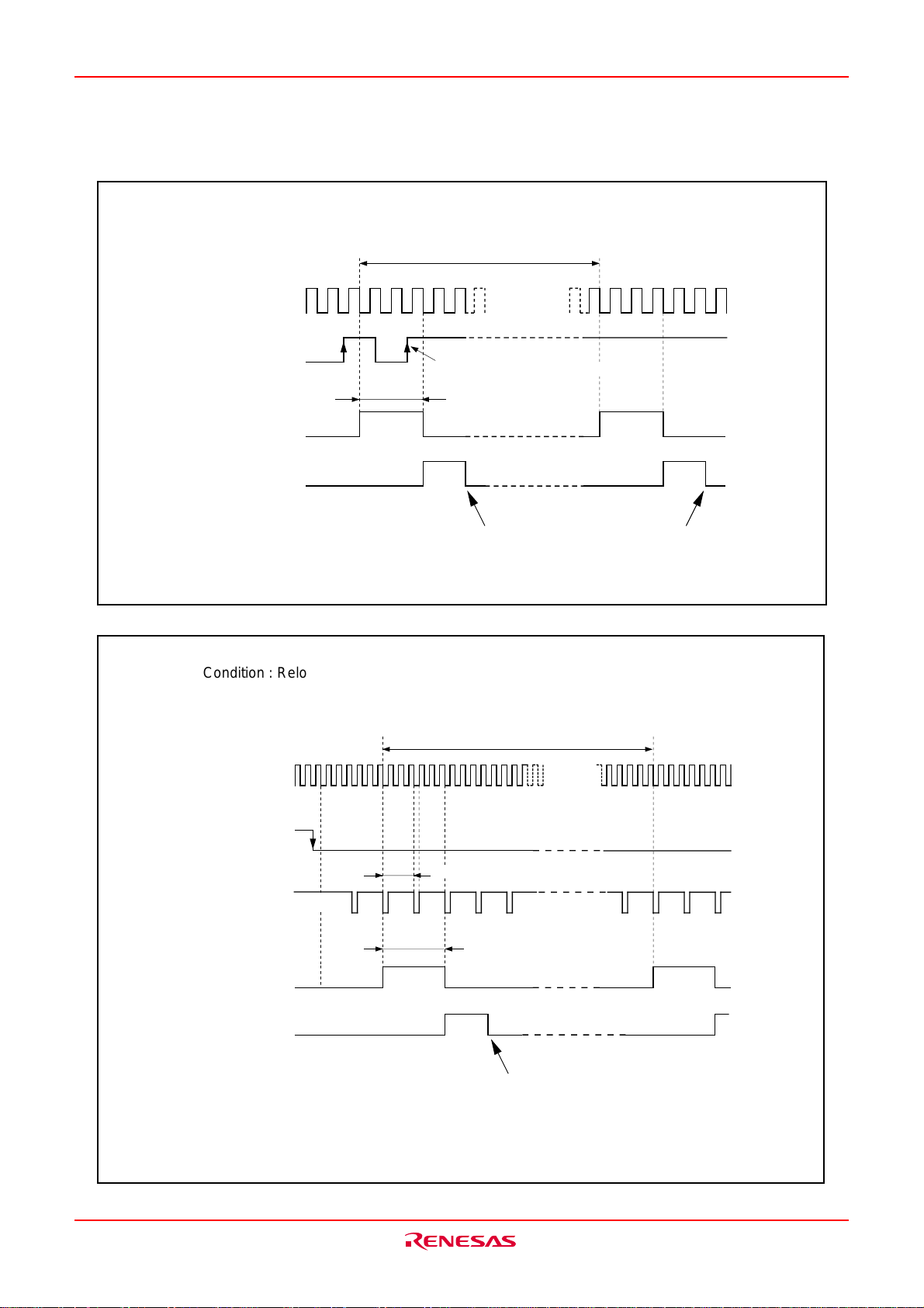
M16C/6KA Group
Timer A
Condition : Reload register = 000316, when external trigger
Count source
(rising edge of TA
iIN
pin input signal) is selected
16
1 / fi X (2 – 1)
pin
“H”
“L”
“H”
“L”
“1”
“0”
Trigger is not generated by this signal
1 / f
i
X
n
TA
iIN
pin
input signal
PWM pulse output
iOUT
from TA
Timer Ai interrupt
request bit
fi : Frequency of count source
(f
1
, f8, f32)
Note: n = 0000
16
to FFFE16.
Cleared to “0” when interrupt request is accepted, or cleared by software
Fig.FB-12 Example of how a 16-bit pulse width modulator operates
Condition : Reload register high-order 8 bits = 02
Reload register low-order 8 bits = 02
External trigger (falling edge of TA
1 / fi X (m + 1) X (2 – 1)
Count source (Note1)
16
16
iIN
pin input signal) is selected
8
iIN
pin input signal
TA
Underflow signal of
8-bit prescaler (Note2)
PWM pulse output
from TA
iOUT
pin
Timer Ai interrupt
request bit
“H”
“L”
1 / fi X (m + 1)
“H”
“L”
1 / fi X (m + 1) X n
“H”
“L”
“1”
“0”
fi : Frequency of count source
(f
1
, f8, f32)
Note 1: The 8-bit prescaler counts the count source.
Note 2: The 8-bit pulse width modulator counts the 8-bit prescaler's underflow signal.
Note 3: m = 00
16
Cleared to “0” when interrupt request is accepted, or cleared by software
to FE16; n = 0016 to FE16.
Fig.FB-13 Example of how an 8-bit pulse width modulator operates
Rev.1.00 Jul 16, 2004 page 78 of 266
REJ03B0100-0100Z
Page 79

M16C/6KA Group Timer B
Timer B
Fig.FB-14 shows the block diagram of timer B. Fig.FB-15 and FB-16 show the timer B-related registers.
Use the timer Bi mode register (i = 0 to 5) bits 0 and 1 to choose the desired mode.
Timer B has three operation modes listed as follows:
• Timer mode: The timer counts an internal count source.
• Event counter mode: The timer counts pulses from an external source or a timer overflow.
• Pulse period/pulse width measuring mode: The timer measures an external signal's pulse period or
pulse width.
Data bus high-order bits
Clock source selection
f
IN
TBi
(i = 0 to 5)
1
f
8
f
32
Polarity switching
and edge pulse
Can be selected in only
event counter mode
TBj overflow
(j = i – 1. Note, however,
j = 2 when i = 0,
j = 5 when i = 3)
• Timer
• Pulse period/pulse width measurement
• Event counter
Fig.FB-14 Block diagram of timer B
Timer Bi mode register
b7 b6 b5 b4 b3 b2 b1 b0
Symbol Address When reset
TBiMR(i = 0 to 5) 039B
TMOD0
TMOD1
Count start flag
(address 038016)
16
to 039D1600XX00002
035B
16
to 035D1600XX00002
Bit name
Operation mode selection
bits
Data bus low-order bits
Counter reset circuit
TBi Address TBj
Timer B0 0391
Timer B1 0393
Timer B2 0395
Timer B3 0351
Timer B4 0353
Timer B5 0355
b1 b0
0 0 : Timer mode
0 1 : Event counter mode
1 0 : Pulse period/pulse width
1 1 : Inhibited
FunctionBit symbol
measurement mode
Low-order 8 bits
Reload register (16)
Counter (16)
16
039016Timer B2
16
039216Timer B0
16
039416 Timer B1
16
035016Timer B5
16
035216Timer B3
16
035416 Timer B4
High-order 8 bits
WR
MR0
MR1
MR2
MR3
TCK0
TCK1
Note 1: Timer B0, timer B3.
Note 2: Timer B1, timer B2, timer B4, timer B5.
Fig.FB-15 Timer B-related registers (1)
Rev.1.00 Jul 16, 2004 page 79 of 266
REJ03B0100-0100Z
Function varies with each operation mode
(Note 1)
(Note 2)
Count source selection bits
(Function varies with each operation mode)
Page 80

M16C/6KA Group Timer B
AAAAAAAAAAAAAAA
AAAAAAAAAAAAAAA
AAAAAAAAAAAAAAA
AAAAAAAAAAAAAAA
AAAAAAAAAAAAAAA
AAAAAAAAAAAAAAA
A
A
A
A
A
A
AAAAAAAAAAAAAAA
Timer Bi register (Note)
(b15) (b8)
b7 b0 b7 b0
• Timer mode 000016 to FFFF16
Counts the timer's period
• Event counter mode 000016 to FFFF
Counts external pulses input or a timer overflow
• Pulse period / pulse width measurement mode
Measures a pulse period or width
Note: Read and write data in 16-bit units.
Count start flag
b7 b6 b5 b4 b3 b2 b1 b0
Symbol Address When reset
TABSR 0380
Bit symbol
TA0S
TA1S
TA2S
TA3S
TA4S
TB0S
TB1S
TB2S
Symbol Address When reset
TB0 0391
TB1 0393
TB2 0395
TB3 0351
TB4 0353
TB5 0355
Function
16
Bit name
Timer A0 count start flag
Timer A1 count start flag
Timer A2 count start flag
Timer A3 count start flag
Timer A4 count start flag
Timer B0 count start flag
Timer B1 count start flag
Timer B2 count start flag
16
, 039016Indeterminate
16
, 039216Indeterminate
16
, 039416Indeterminate
16
, 035016Indeterminate
16
, 035216Indeterminate
16
, 035416Indeterminate
Values that can be set
00
16
Function
0 : Stops counting
1 : Starts counting
WR
16
WR
Timer B3, 4, 5 count start flag
b7 b6 b5 b4 b3 b2 b1 b0
Symbol Address When reset
TBSR 0340
Bit symbol
Nothing is assigned.
AAAAAAAAAAAAA
In an attempt to write to these bits, write “0”. The value, if read, turns out to be
indeterminate.
AAAAAAAAAAAAA
TB3S
AAAAAAAAAAAAA
TB4S
TB5S
Timer B3 count start flag
Timer B4 count start flag
Timer B5 count start flag
16
Bit name
Fig.FB-16 Timer B-related registers (2)
Rev.1.00 Jul 16, 2004 page 80 of 266
REJ03B0100-0100Z
000XXXXX
2
0 : Stops counting
1 : Starts counting
Function
WR
Page 81

M16C/6KA Group Timer B
(1) Timer mode
In this mode, the timer counts an internally generated count source. (See Table.FB-6.) Fig.FB-17 shows the
timer Bi mode register in timer mode.
Table.FB-6 Timer specifications in timer mode
Item Specification
Count source f1, f8, f32
Count operation •Counts down
•When the timer underflows, it reloads the reload register contents and
then continuing counting
Divide ratio 1/(n+1) n : Set value
Count start condition Count start flag is set (= 1)
Count stop condition Count start flag is reset (= 0)
Interrupt request generation timing
TBiIN pin function Programmable I/O port
Read from timer Count value is read out by reading timer Bi register
Write to timer •When counting stopped
The timer underflows
When a value is written to timer Bi register, it is written to both reload register and counter
• When counting in progress
When a value is written to timer Bi register, it is written to only reload register
(Transferred to counter at next reload time)
Timer Bi mode register
b7 b6 b5 b4 b3 b2 b1 b0
0
0
Note 1: Timer B0, timer B3.
Note 2: Timer B1, timer B2, timer B4, timer B5.
Symbol Address When reset
TBiMR(i=0 to 5) 039B
Bit symbol WR
TMOD0
TMOD1
MR0
MR1
MR2
MR3
TCK0
TCK1
Operation mode selection
bits
Invalid in timer mode
Can be “0” or “1”
0 (Set to “0” in timer mode ; i = 0, 3)
Nothing is assigned (i = 1, 2, 4, 5).
In an attempt to write to this bit, write “0”. The value, if read, turns out
to be indeterminate.
Invalid in timer mode.
In an attempt to write to this bit, write “0”. The value, if read in
timer mode, turns out to be indeterminate.
Count source selection bits
16
to 039D
035B16 to 035D
16
16
00XX0000
00XX0000
2
2
Bit name Function
b1 b0
0 0 : Timer mode
b7 b6
1
0 0 : f
0 1 : f
8
1 0 : f
32
1 1 : Inhibited
(Note 1)
(Note 2)
Fig.FB-17 Timer Bi mode register in timer mode
Rev.1.00 Jul 16, 2004 page 81 of 266
REJ03B0100-0100Z
Page 82

M16C/6KA Group Timer B
(2) Event counter mode
In this mode, the timer counts an external signal or an internal timer's overflow. (See Table.FB-7) Fig.FB-18
shows the timer Bi mode register in event counter mode.
Table.FB-7 Timer specifications in event counter mode
Item Specification
Count source •External signals input to TBiIN pin
•Effective edge of count source can be a rising edge, a falling edge, or both
edges as selected by software
Count operation •Counts down
•When the timer underflows, it reloads the reload register contents and
then continuing counting
Divide ratio 1/(n+1) n : Set value
Count start condition Count start flag is set (= 1)
Count stop condition Count start flag is reset (= 0)
Interrupt request generation timing
TBiIN pin function Count source input
Read from timer Count value can be read out by reading timer Bi register
Write to timer •When counting stopped
The timer underflows
When a value is written to timer Bi register, it is written to both reload register and counter
•When counting in progress
When a value is written to timer Bi register, it is written to only reload register
(Transferred to counter at next reload time)
Timer Bi mode register
b7 b6 b5 b4 b3 b2 b1 b0
01
Symbol Address When reset
TBiMR(i=0 to 5) 039B
TMOD0
TMOD1
TCK0
TCK1
Note 1: Valid only when input from the TBiIN pin is selected as the event clock.
Note 2: Timer B0, timer B3.
Note 3: Timer B1, timer B2, timer B4, timer B5.
Note 4: Set the corresponding port direction register to “0”.
Operation mode selection
bits
Count polarity selection
MR0
bits
MR1
0 (Fixed to “0” in event counter mode; i = 0, 3)
MR2
Nothing is assigned (i = 1, 2, 4, 5).
In an attempt to write to this bit, write “0”. The value, if read,
turns out to be indeterminate.
Invalid in event counter mode.
MR3
In an attempt to write to this bit, write “0”. The value, if read in
event counter mode, turns out to be indeterminate.
Invalid in event counter mode.
Can be “0” or “1”.
Event clock selection
If timer's overflow is selected, this bit can be “0” or “1”.
16
to 039D1600XX0000
035B16 to 035D1600XX0000
Bit name FunctionBit symbol
(Note 1)
b1 b0
0 1 : Event counter mode
b3 b2
0 0 : Counts external signal's
0 1 : Counts external signal's
1 0 : Counts external signal's
1 1 : Inhibited
0 : Input from TBi
1 : TBj overflow
2
2
falling edges
rising edges
falling and rising edges
IN
pin (Note 4)
(j = i – 1; however, j = 2 when i = 0,
j = 5 when i = 3)
WR
(Note 2)
(Note 3)
Fig.FB-18 Timer Bi mode register in event counter mode
Rev.1.00 Jul 16, 2004 page 82 of 266
REJ03B0100-0100Z
Page 83

M16C/6KA Group Timer B
(3) Pulse period/pulse width measurement mode
In this mode, the timer measures the pulse period or pulse width of an external signal. (See Table.FB-8)
Fig.FB-19 shows the timer Bi mode register in pulse period/pulse width measurement mode. Fig.FB-20
shows the operation timing when measuring a pulse period. Fig.FB-21 shows the operation timing when
measuring a pulse width.
Table.FB-8 Timer specifications in pulse period/pulse width measurement mode
Item Specification
Count source f1, f8, f32
Count operation •Up count
•At measurement pulse's effective edge, after the count value is transferred
to reload register, it is cleared to "000016" and then continues counting.
Count start condition Count start flag is set (= 1)
Count stop condition Count start flag is reset (= 0)
Interrupt request generation timing
TBiIN pin function Measurement pulse input
Read from timer When timer Bi register is read, it indicates the reload register’s content
Write to timer Cannot be written to
Note 1 : An interrupt request is not generated when the first effective edge is input after the timer has started counting.
Note 2 : After count starts, the value read out from the timer Bi register is indeterminate until the second effective edge
is input .
•When measurement pulse's effective edge is input (Note 1)
•When an overflow occurs. (Simultaneously, the timer Bi overflow flag becomes
“1”. The timer Bi overflow flag becomes “0” when the count start flag is “1”
and a value is written to the timer Bi mode register.)
(measurement result) (Note 2)
Timer Bi mode register
b7 b6 b5 b4 b3 b2 b1 b0
Symbol Address When reset
TBiMR(i=0 to 5) 039B
01
TMOD0
TMOD1
Note 1: The timer Bi overflow flag becomes “0” when the count start flag is “1” and a value is written to the
Note 2: Timer B0, timer B3.
Note 3: Timer B1, timer B2, timer B4, timer B5.
Operation mode
selection bits
MR0
Measurement mode
selection bits
MR1
0 (Fixed to “0” in pulse period/pulse width measurement mode; i = 0, 3)
MR2
Nothing is assigned (i = 1, 2, 4, 5).
In an attempt to write to this bit, write “0”. The value, if read, turns out to be
indeterminate.
Timer Bi overflow
MR3
flag ( Note 1)
Count source
TCK0
selection bits
TCK1
timer Bi mode register. This flag cannot be set to “1” by software.
16
to 039D1600XX0000
035B
16
to 035D1600XX0000
Bit nameBit symbol
b1 b0
1 0 : Pulse period / pulse width
measurement mode
b3 b2
0 0 : Pulse period measurement (Interval between
measurement pulse's falling edge to falling edge)
0 1 : Pulse period measurement (Interval between
measurement pulse's rising edge to rising edge)
1 0 : Pulse width measurement (Interval between
measurement pulse's falling edge to rising edge,
and between rising edge to falling edge)
1 1 : Inhibited
0 : Timer did not overflow
1 : Timer has overflowed
b7 b6
0 0 : f
1
0 1 : f
8
1 0 : f
32
1 1 : Inhibited
2
2
Function
(Note 2)
(Note 3)
Fig.FB-19 Timer Bi mode register in pulse period/pulse width measurement mode
WR
Rev.1.00 Jul 16, 2004 page 83 of 266
REJ03B0100-0100Z
Page 84

M16C/6KA Group Timer B
When measuring a pulse time interval from falling edge to falling edge
Count source
Measurement pulse
“H”
“L”
Transfer
(indeterminate value)
Reload register counter
transfer timing
Timing at which counter
reaches “0000
Count start flag
Timer Bi interrupt
request bit
16
”
“1”
“0”
“1”
“0”
Cleared to “0” when interrupt request is accepted, or cleared by software.
Timer Bi overflow flag
“1”
“0”
Note 1: Counter is initialized at completion of measurement.
f
Fig.FB-20 Operation timing when measuring a pulse period
Count source
Transfer
(measured value)
(Note 1)(Note 1)
(Note 2)
Measurement pulse
Reload register counter
“H”
“L”
Transfer
(indeterminate
value)
transfer timing
Timing at which counter
reaches “0000
Count start flag
Timer Bi interrupt
request bit
Timer Bi overflow flag
16
”
“1”
“0”
“1”
“0”
“1”
“0”
Cleared to “0” when interrupt request is accepted, or cleared by software.
Note 1: Counter is initialized at completion of measurement.
Note 2: Timer has overflowed.
Fig.FB-21 Operation timing when measuring a pulse width
Rev.1.00 Jul 16, 2004 page 84 of 266
REJ03B0100-0100Z
Transfer
(measured value)
Transfer
(measured
value)
(Note 1)
Transfer
(measured value)
(Note 1)(Note 1)(Note 1)
(Note 2)
Page 85

M16C/6KA Group
Serial I/O
Serial I/O
Serial I/O is configured as three channels: UART1, S I/O3 and S I/O4.
UART1
Fig.GA-1 shows the block diagram of UART1. Fig.GA-2 shows the block diagram of the transmit/receive
unit.
UART1 has two operation modes: a clock synchronous serial I/O mode and a clock asynchronous serial I/O
mode (UART mode). The contents of the serial I/O mode selection bits (bits 0 to 2 at address 03A816) determine whether UART1 is used as a clock synchronous serial I/O or as a UART. Although a few functions are
different, UART1 has almost the same functions.
Table.GA-1 shows the functions of UART1, and Fig.GA-3 to GA-7 show the registers related to UART1.
Table.GA-1 Functions of UART1
Function
CLK polarity selection
LSB first / MSB first selection
Continuous receive mode selection
Transfer clock output from multiple
pins selection
Serial data logic switch
TxD, RxD I/O polarity switch
TxD, RxD port output format
Note 1: Only in clock synchronous serial I/O mode.
UART1
Possible (Note 1)
Possible (Note 1)
Possible (Note 1)
Possible (Note 1)
Possible
Possible
CMOS output
Rev.1.00 Jul 16, 2004 page 85 of 266
REJ03B0100-0100Z
Page 86

M16C/6KA Group
Serial I/O
(UART1)
RxD
CLK
CTS1 / RTS
/ CLKS
1
Clock source selection
f
1
f
8
f
32
1
1
1
RxD polarity
switching circuit
CLK
polarity
switching
circuit
Bit rate generator
Internal
(address 03A9
1 / (n1+1)
External
Clock synchronous type
(when internal clock is selected)
Clock output pin
select switch
Fig.GA-1 Block diagram of UART1
UART reception
1/16
Clock synchronous type
16
)
UART transmission
1/16
Clock synchronous type
Clock synchronous type
(when internal clock is selected)
1/2
CTS/RTS disabled
V
CC
CTS/RTS disabled
Clock synchronous type
(when external clock is
selected)
RTS
CTS
n1 : Values set to UART1 bit rate generator (BRG1)
Reception
control circuit
Transmission
control circuit
1
1
Receive
clock
Transmit
clock
Transmit/
receive
unit
TxD
polarity
switching
circuit
TxD
1
Rev.1.00 Jul 16, 2004 page 86 of 266
REJ03B0100-0100Z
Page 87

M16C/6KA Group
Serial I/O
RXD
RxD data
1
reverse circuit
1SP
SP SP
2SP
0000000
No reverse
Reverse
PAR
PAR
disabled
PAR
enabled
Clock
synchronous
type
UART
Clock
synchronous type
UART
(7 bits)
UART
(8 bits)
UART
(9 bits)
D
8
UART(7 bits)
Clock
synchronous type
UART
(8 bits)
UART
(9 bits)
UART1 receive register
D7D6D5D4D3D2D1D
Logic reverse circuit + MSB/LSB conversion circuit
0
UART1 receive
buffer register
Address 03AE
Address 03AF
16
16
Data bus high-order bits
Data bus low-order bits
Logic reverse circuit + MSB/LSB conversion circuit
SP SP
2SP
1SP
PAR
PAR
enabled
PAR
disabled
“0”
UART
Clock
synchronous
type
D
UART
(9 bits)
UART
(7 bits)
UART
(8 bits)
Clock
synchronous type
8
D7D6D5D4D3D2D1D
UART
(8 bits)
UART
(9 bits)
Clock
synchronous type
UART(7 bits)
UART1 transmit register
Not reverse
TxD data
reverse circuit
Reverse
0
TXD
SP: Stop bit
PAR: Parity bit
UART1 transmit
buffer register
Address 03AA
Address 03AB
1
16
16
Fig.GA-2 Block diagram of UART1 transmit/receive unit
Rev.1.00 Jul 16, 2004 page 87 of 266
REJ03B0100-0100Z
Page 88

M16C/6KA Group
UART1 transmit buffer register
(b15) (b8)
b7 b0
Serial I/O
b7 b0
Symbol Address When reset
U1TB 03AB
16
, 03AA16Indeterminate
UART1 receive buffer register
(b15)
b7 b0
(b8)
b7 b0
Function
Transmit data
Nothing is assigned.
In an attempt to write to these bits, write “0”. The value, if read, turn out to be indeterminate.
Symbol Address When reset
Bit
symbol
U1RB 03AF
Bit name
16
, 03AE16Indeterminate
Function
(During clock synchronous
serial I/O mode)
Receive data
Function
(During UART mode)
Receive data
Nothing is assigned.
In an attempt to write to these bits, write “0”. The value, if read, turns out to be “0”.
Overrun error flag (Note 1)
OER
FER
Framing error flag (Note 1)
0 : No overrun error
1 : Overrun error found
Invalid
0 : No overrun error
1 : Overrun error found
0 : No framing error
1 : Framing error found
PER
Parity error flag (Note 1)
Invalid
0 : No parity error
1 : Parity error found
SUM
Error sum flag (Note 1)
Invalid
0 : No error
1 : Error found
WR
WR
Note 1: Bits 15 through 12 are set to “0” when the serial I/O mode selection bits (bits 2 to 0 at address
03A8
(Bit 15 is set to “0” when bits 14 to 12 all are set to “0”.) Bits 14 and 13 are also set to “0” when the
lower byte of the UART1 receive buffer register (address 03AE
UART1 bit rate generator
b7
b0
Assuming that set value = n, BRG1 divides the count source by
n + 1
Fig.GA-3 Serial I/O-related registers (1)
16
) are set to “0002” or the receive enable bit is set to “0”.
Symbol Address When reset
U1BRG 03A9
16
Indeterminate
Function
16
) is read out.
Values that can be set
0016 to FF
16
WR
Rev.1.00 Jul 16, 2004 page 88 of 266
REJ03B0100-0100Z
Page 89

M16C/6KA Group
UART1 transmit/receive mode register
b7 b6 b5 b4 b3 b2 b1 b0
Serial I/O
Symbol Address When reset
U1MR 03A8
16 0016
Bit
symbol
SMD0
SMD1
SMD2
CKDIR
STPS
PRY
PRYE
SLEP
IOPOL
Note 1: Set the corresponding port direction register to "0".
Bit name
Serial I/O mode selection
bits
Internal/external clock
selection bit
Stop bit length selection
bit
Odd/even parity selection
bit
Parity enable bit
Sleep selection bit
TxD, RxD I/O polarity
switching bit
Fig.GA-4 Serial I/O-related registers (2)
Function
(During clock synchronous
serial I/O mode)
Must be fixed to 001
b2 b1 b0
0 0 0 : Serial I/O invalid
0 1 0 : Inhibited
0 1 1 : Inhibited
1 1 1 : Inhibited
0 : Internal clock
1 : External clock (Note 1)
Invalid
Invalid
Invalid
Must always be “0”
0 : Not reverse
1 : Reverse
Usually set to “0”
Function
(During UART mode)
b2 b1 b0
1 0 0 : Transfer data 7 bits long
1 0 1 : Transfer data 8 bits long
1 1 0 : Transfer data 9 bits long
0 0 0 : Serial I/O invalid
0 1 0 : Inhibited
0 1 1 : Inhibited
1 1 1 : Inhibited
Must always be "0"
0 : One stop bit
1 : Two stop bits
Valid when bit 6 = “1”
0 : Odd parity
1 : Even parity
0 : Parity disabled
1 : Parity enabled
0 : Sleep mode deselected
1 : Sleep mode selected
0 : Not reverse
1 : Reverse
Usually set to “0”
WR
Rev.1.00 Jul 16, 2004 page 89 of 266
REJ03B0100-0100Z
Page 90

M16C/6KA Group
y
Serial I/O
UART1 transmit/receive control register 0
b7 b6 b5 b4 b3 b2 b1 b0
Symbol Address When reset
U1C0 03AC
16
08
16
Bit
symbol
CLK0
Bit name
BRG count source
selection bits
CLK1
CTS/RTS function
CRS
selection bit
TXEPT
Transmit register empty
flag
CRD
CTS/RTS disable bit
Data output selection bit
NCH
CLK polarity selection bit
CKPOL
UFORM Transfer format selection
bit (Note 3)
Function
(During clock synchronous
b1 b0
0 0 : f1 is selected
0 1 : f
1 0 : f
1 1 : Inhibited
Valid when bit 4 = “0”
0 : CTS function is selected (Note 1)
1 : RTS function is selected (Note 2)
0 : Data present in transmit register
1 : No data present in transmit
0 : CTS/RTS function enabled
1 : CTS/RTS function disabled
0 : TXD1 pin is CMOS output
1 : T
0 : Transmit data is output at
1 : Transmit data is output at
serial I/O mode)
8
is selected
32
is selected
(during transmission)
register (transmission completed)
(Pins function as
programmable I/O port)
XD1
pin is N-channel open-
drain output
falling edge of transfer clock
and receive data is input at
rising edge
rising edge of transfer clock
and receive data is input at
falling edge
0 : LSB first
1 : MSB first
Function
(During UART mode)
b1 b0
0 0 : f1 is selected
8
is selected
0 1 : f
1 0 : f
32
is selected
1 1 : Inhibited
Valid when bit 4 = “0”
0 : CTS function is selected (Note 1)
1 : RTS function is selected (Note 2)
0 : Data present in transmit register
(during transmission)
1 : No data present in transmit
register (transmission completed)
0 : CTS/RTS function enabled
1 : CTS/RTS function disabled
(Pins function as programmable
I/O port)
XD1
pin is CMOS output
0: T
XD1
pin is N-channel open-drain
1: T
output
Must always be “0”
0 : LSB first
1 : MSB first
WR
Note 1: Set the corresponding port direction register to “0”.
Note 2: The settings of the corresponding port register and port direction register are invalid.
Note 3: Onl
clock synchronous serial I/O mode and 8-bit UART mode are valid.
Fig.GA-5 Serial I/O-related registers (3)
Rev.1.00 Jul 16, 2004 page 90 of 266
REJ03B0100-0100Z
Page 91

M16C/6KA Group
Serial I/O
UART1 transmit/receive control register 1
b7 b6 b5 b4 b3 b2 b1 b0
Symbol Address When reset
U1C1 03AD
Bit
symbol
TE
TI
RE
RI
Nothing is assigned.
In an attempt to write to these bits, write “0”. The value, if read, turns out to be “0”.
U1LCH
Nothing is assigned.
In an attempt to write to these bits, write “0”. The value, if read, turns out to be “0”.
Bit name
Transmit enable bit
Transmit buffer empty flag
Receive enable bit
Receive complete flag
Data logic selection bit
16
(During clock synchronous
0 : Transmission disabled
1 : Transmission enabled
0 : Data present in
1 : No data present in
0 : Reception disabled
1 : Reception enabled
0 : No data present in
1 : Data present in
0 : Not reverse
1 : Reverse
02
16
Function
serial I/O mode)
transmit buffer register
transmit buffer register
receive buffer register
receive buffer register
(During UART mode)
0 : Transmission disabled
1 : Transmission enabled
0 : Data present in
transmit buffer register
1 : No data present in
transmit buffer register
0 : Reception disabled
1 : Reception enabled
0 : No data present in
receive buffer register
1 : Data present in
receive buffer register
0 : Not reverse
1 : Reverse
Function
WR
Fig.GA-6 Serial I/O-related registers (4)
Rev.1.00 Jul 16, 2004 page 91 of 266
REJ03B0100-0100Z
Page 92

M16C/6KA Group
Serial I/O
UART transmit/receive control register 2
b7 b6 b5 b4 b3 b2 b1 b0
0
0
0
Symbol Address When reset
UCON 03B0
16
X0000000
2
Bit
symbol
Reserved bit Must always be “0”
U1IRS
Reserved bit Must always be “0”
U1RRM
CLKMD0
CLKMD1
Reserved bit Must always be “0”
Nothing is assigned.
In an attempt to write to this bit, write “0”. The value, if read, turns out to be indeterminate.
Note: When using multiple pins to output the transfer clock, the following requirements must be met:
• UART1 internal/external clock selection bit (bit 3 at address 03A8
Bit name
UART1 transmit interrupt
factor selection bit
UART1 continuous
receive mode enable bit
CLK/CLKS selection bit 0
CLK/CLKS selection bit 1
(Note)
0 : Transmit buffer empty (Tl = 1)
1 : Transmission completed
0 : Continuous receive mode
1 : Continuous receive mode
Valid when bit 5 = “1”
0 : Clock output to CLK1
1 : Clock output to CLKS1
0 : Normal mode
1 : Transfer clock output from
Function
(During clock synchronous
serial I/O mode)
(TXEPT = 1)
disabled
enabled
(CLK output is CLK1 only)
multiple pins function selected
0 : Transmit buffer empty (Tl = 1)
1 : Transmission completed
Invalid
Invalid
Must always be “0”
16
) = “0”.
Function
(During UART mode)
(TXEPT = 1)
WR
Fig.GA-7 Serial I/O-related registers (5)
Rev.1.00 Jul 16, 2004 page 92 of 266
REJ03B0100-0100Z
Page 93

M16C/6KA Group
Clock synchronous serial I/O mode
(1) Clock synchronous serial I/O mode
The clock synchronous serial I/O mode uses a transfer clock to transmit and receive data. Tables.GA-2 and
GA-3 list the specifications of the clock synchronous serial I/O mode. Fig.GA-8 shows the UART1 transmit/
receive mode register.
Table.GA-2 Specifications of clock synchronous serial I/O mode (1)
Item Specification
Transfer data format • Transfer data length: 8 bits
Transfer clock • When internal clock is selected (bit 3 at address 03A816 = “0” ) :
fi/ 2(n+1) (Note 1) fi = f1, f8, f32
• When external clock is selected (bit 3 at address 03A816 = “1” ) :
Input from CLK1 pin
Transmission/reception control
Transmission start condition
• Selecting from CTS function/RTS function/Disable CTS, RTS function
• To start transmission, the following requirements must be met:
_
Transmit enable bit (bit 0 at address 03AD16) = “1”
_
Transmit buffer empty flag (bit 1 at address 03AD16) = “0”
_
When CTS function selected, CTS input level = “L”
•
Furthermore, if external clock is selected, the following requirements must also be met:
_
CLK1 polarity select bit (bit 6 at address 03AC16) = “0”:
_______ _______
CLK1 input level = “H”
_
CLK1 polarity select bit (bit 6 at address 03AC16) = “1”:
CLK1 input level = “L”
Reception start condition • To start reception, the following requirements must be met:
_
Receive enable bit (bit 2 at address 03AD16) = “1”
_
Transmit enable bit (bit 0 at address 03AD16) = “1”
_
Transmit buffer empty flag (bit 1 at address 03AD16) = “0”
• Furthermore, if external clock is selected, the following requirements must
also be met:
_
CLK1 polarity select bit (bit 6 at address 03AC16) = “0”:
CLK1 input level = “H”
_
CLK1 polarity select bit (bit 6 at address 03AC16) = “1”:
CLK1 input level = “L”
• When transmitting
_
Interrupt request
generation timing
Transmit interrupt factor selection bit (bit 1 at address 03B016) = “0”:
At the completion of data transmission from UART1 transfer buffer register
to UART1 transmit register
_
Transmit interrupt factor selection bit (bit 1 at address 03B016) = “1”:
At the completion of data transmission from UART1 transfer register is
completed
• When receiving
_
At the completion of data transferring from UART1 receive register to
UART1 receive buffer register
Error detection • Overrun error (Note 2)
This error occurs when bit 7 of next data is received before the contents of
UART1 receive buffer register are read out.
Note 1: “n” denotes the value 0016 to FF16 that is set to the UART bit rate generator.
Note 2: If an overrun error occurs, the UART1 receive buffer will have the next data written in. Note also that
the UART1 receive interrupt request bit is not set to “1”.
_______ _______ _______ _______
Rev.1.00 Jul 16, 2004 page 93 of 266
REJ03B0100-0100Z
Page 94

M16C/6KA Group
Clock synchronous serial I/O mode
Table.GA-3 Specifications of clock synchronous serial I/O mode (2)
Item Specification
Function selection • CLK polarity selection
Whether transmit data is output/input at the rising edge or falling edge of the
transfer clock can be selected
• LSB first/MSB first selection
Whether transmission/reception begins with bit 0 or bit 7 can be selected
• Continuous receive mode selection
Reception is enabled simultaneously by a read from the receive buffer register
• Transfer clock output from multiple pins selection
UART1 transfer clock can be chosen by software to be output from one of
the two pins set
Rev.1.00 Jul 16, 2004 page 94 of 266
REJ03B0100-0100Z
Page 95

M16C/6KA Group
Clock synchronous serial I/O mode
UART1 transmit/receive mode registers
b7 b6 b5 b4 b3 b2 b1 b0
010
Symbol Address When reset
U1MR 03A8
SMD0
SMD1
SMD2
CKDIR
STPS
PRY
PRYE
IOPOL
16
00
16
Bit name FunctionBit symbol WR
Serial I/O mode selection bits
b2 b1 b0
0 0 1 : Clock synchronous serial
I/O mode
Internal/external clock
selection bit
0 : Internal clock
1 : External clock (Note 1)
Invalid in clock synchronous serial I/O mode
TxD, RxD I/O polarity
reverse bit (Note 1)
0 : No reverse
1 : Reverse
Note 1: Usually sent to "0".
Note 2: The corresponding port direction register should be "0".
Fig.GA-8 UART1 transmit/receive mode register in clock synchronous serial I/O mode
Rev.1.00 Jul 16, 2004 page 95 of 266
REJ03B0100-0100Z
Page 96

M16C/6KA Group
Clock synchronous serial I/O mode
Table.GA-4 lists the functions of the input/output pins during clock synchronous serial I/O mode. This table
shows the pin functions that the transfer clock output from multiple pins are not selected. Note that for a
period from when the UART1 operation mode is selected to when transfer starts, the TxD1 pin outputs a “H”.
(If the N-channel open-drain is selected, this pin is in floating state.)
Table.GA-4 Input/output pin functions in clock synchronous serial I/O mode
(The function that the transfer clock output from multiple pin is not selected.)
Pin name Function Method of selection
TxD
RxD
1
1
Serial data output
Serial data input
(Outputs dummy data when performing reception only)
The corresponding bit of port direction register = “0”
(Can be used as an input port when performing transmission only)
CLK1
CTS1/RTS1
Transfer clock output
Transfer clock input
CTS input
RTS output
Programmable I/O port
Internal/external clock select bit (bit 3 at address 03A816) = “0”
Internal/external clock select bit (bit 3 at address 03A8
The corresponding bit of port direction register = “0”
CTS/RTS disable bit (bit 4 at address 03AC
CTS/RTS function selection bit (bit 2 at address 03AC
The corresponding port direction bit = “0”
CTS/RTS disable bit (bit 4 at address 03AC16) = “0”
CTS/RTS function selection bit (bit 2 at address 03AC
CTS/RTS disable bit (bit 4 at address 03AC16) = “1”
16) =“0”
16) = “1”
16) = “0”
16) = “1”
Rev.1.00 Jul 16, 2004 page 96 of 266
REJ03B0100-0100Z
Page 97

M16C/6KA Group
Clock synchronous serial I/O mode
• Example of transmit timing (when internal clock is selected)
Tc
Transfer clock
Transmit enable
bit (TE)
Transmit buffer
empty flag (Tl)
CTS
1
CLK
1
TxD
1
Transmit
register empty
flag (TXEPT)
Transmit interrupt
request bit (IR)
“1”
“0”
Data is set in UART1 transmit buffer register
“1”
“0”
“H”
“L”
“1”
“0”
“1”
“0”
D
0
Transferred from UART1 transmit buffer register to UART1 transmit register
T
CLK
D
3
D
2
D
1
Stopped because CTS = “H”
D
7
D
D
4
D
5
D
6
0
D
3
D
2
D
1
Cleared to “0” when interrupt request is accepted, or cleared by software
Shown in ( ) are bit symbols.
The above timing applies to the following settings:
• Internal clock is selected.
• CTS function is selected.
• CLK polarity selection bit = “0”.
• Transmit interrupt factor selection bit = “0”.
Tc = TCLK = 2(n + 1) / fi
fi: frequency of BRG1 count source (f
n: value set to BRG1
• Example of receive timing (when external clock is selected)
Receive enable
bit (RE)
Transmit enable
bit (TE)
Transmit buffer
empty flag (Tl)
RTS
1
CLK
1
RxD
1
Receive complete
flag (Rl)
Receive interrupt
request bit (IR)
Shown in ( ) are bit symbols.
“1”
“0”
“1”
“0”
“1”
“0”
“H”
“L”
Transferred from UART1 receive register
“1”
“0”
“1”
“0”
Dummy data is set in UART1 transmit buffer register
Transferred from UART1 transmit buffer register to UART1 transmit register
D
0
to UART1 receive buffer register
D
D
2
D
1
Cleared to “0” when interrupt request is accepted, or cleared by software
1 / f
EXT
Receive data is taken in
3
D
4
D
5
D
6
D
0
D
2
D
1
D
D
7
Read out from UART1 receive buffer register
3
Stopped because transfer enable bit = “0”
D
D
4
D
4
7
D
5
D
6
D
5
D
0
D
D
1
1
, f8, f32)
D
3
2
D
4
D
7
D
5
D
6
The above timing applies to the following settings:
• External clock is selected.
• RTS function is selected.
• CLK polarity selection bit = “0”.
fEXT: frequency of external clock
The following conditions should be matched when the input level of
1
pin is "H" before the data reception.
CLK
• Transmit enable bit “1”
• Receive enable bit “1”
• Dummy data write to UART1 transmit buffer register
Fig.GA-9 Typical transmit/receive timings in clock synchronous serial I/O mode
Rev.1.00 Jul 16, 2004 page 97 of 266
REJ03B0100-0100Z
Page 98

M16C/6KA Group
Clock synchronous serial I/O mode
(a) Polarity selection function
As shown in Fig.GA-10, the CLK polarity selection bit (bit 6 at address 03AC16) allows to select the polarity
of the transfer clock.
• When CLK polarity selection bit = “0”
CLK
1
TXD
RXD
1
1
D
1
D
1
D2D3D
D2D3D
D
0
D
0
4
D5D6D
4
D5D6D
7
7
Note 1: The CLK pin level is "H" when
there is no transferring.
• When CLK polarity select bit = “1”
CLK
1
Note 2: The CLK pin level is "L" when
TXD
RXD
1
1
D
1
D
1
D2D3D
D2D3D
D
0
D
0
4
D5D6D
4
D5D6D
7
7
there is no transferring.
Fig.GA-10 Polarity of transfer clock
(b) LSB first/MSB first selection function
As shown in Fig.GA-11, when the transfer format selection bit (bit 7 at address 03AC16) = “0”, the transfer
format is “LSB first”; when the bit = “1”, the transfer format is “MSB first”.
• When transfer format selection bit = “0”
CLK
1
D
TXD
RXD
1
1
D
D
1
0
D
1
0
• When transfer format selection bit = “1”
CLK
1
D
TXD
1
RXD
1
Fig.GA-11 Transfer format
Rev.1.00 Jul 16, 2004 page 98 of 266
REJ03B0100-0100Z
7
D
6
D
D
6
7
D
2
D
3
D
4
D
5
D
6
D
7
LSB first
D
2
D
3
D
4
D
5
D
6
D
7
D
5
D
4
D
3
D
2
D
1
D
0
MSB first
D
5
D
4
D
3
D
2
D
1
D
0
Note: This applies when the CLK polarity selection bit = “0”.
Page 99

M16C/6KA Group
Clock synchronous serial I/O mode
(c) Transfer clock output from multiple pins function (UART1)
This function allows to set two transfer clock output pins and chooses one to output a clock by the setting of
CLK and CLKS selection bits (bits 4 and 5 at address 03B016). (See Fig.GA-12) The function is valid only
_______ _______
when the UART1 internal clock is selected. Note that when this function is selected, CTS/RTS function
cannot be used.
Microcomputer
TXD1
CLKS
1
CLK
1
IN
CLK
IN
CLK
Fig.GA-12 The sample of transfer clock output from the multiple pins function
(d) Continuous receive mode
If the continuous receive mode enable bit (bit 3 at address 03B016) are set to “1”, the unit is placed in
continuous receive mode. In this mode, when the receive buffer register is read out, the unit simultaneously
goes to a receive enable state without having to set dummy data to the transmit buffer register back again.
Rev.1.00 Jul 16, 2004 page 99 of 266
REJ03B0100-0100Z
Page 100

M16C/6KA Group Clock asynchronous serial I/O (UART) mode
(2) Clock asynchronous serial I/O (UART) mode
The UART mode allows transmitting and receiving data after setting the desired transfer rate and transfer
data format. Tables.GA-5 and GA-6 list the specifications of the UART mode. Fig.GA-13 shows the UART1
transmit/receive mode register.
Table.GA-5 Specifications of UART Mode (1)
Item Specification
Transfer data format • Character bit (transfer data): 7 bits, 8 bits, or 9 bits as selected
• Start bit: 1 bit
• Parity bit: Odd, even, or nothing as selected
• Stop bit: 1 bit or 2 bits as selected
Transfer clock • When internal clock is selected (bit 3 at address 03A816 = “0”) :
fi/16(n+1) (Note 1) fi = f1, f8, f32
• When external clock is selected (bit 3 at address 03A816 =“1”) :
fEXT/16(n+1)(Note 1) (Note 2)
Transmission/reception control
Transmission start condition
• Selecting from Disable CTS, RTS function
• To start transmission, the following requirements must be met:
- Transmit enable bit (bit 0 at address 03AD16) = “1”
- Transmit buffer empty flag (bit 1 at address 03AD16) = “0”
_______ _______
- When CTS function is selected CTS input level = “L”
Reception start condition • To start reception, the following requirements must be met:
- Receive enable bit (bit 2 at address 03AD16) = “1”
- Start bit detection
Interrupt request • When transmitting
generation timing - Transmit interrupt factor selection bit (bit 1 at address 03B016) = “0”:
At the completion of data transferring from UART1 transfer buffer register to
UART1 transmit register
- Transmit interrupt factor selection bit (bit 1 at address 03B016) = “1”:
At the completion of data transmission from UART1 transfer register
• When receiving
- At the completion of data transferring from UART1 receive register to
UART1 receive buffer register
Error detection • Overrun error (Note 3)
This error occurs when the bit prior to the stop bit of next data is received
before the contents of UART1 receive buffer register are read out.
• Framing error
This error occurs when the number set for stop bits is not detected
• Parity error
This error occurs in the case that parity is enabled and the number of "1" in
parity bit and character bits does not match the number of "1" in parity odd/
even setting.
• Error sum flag
This flag is set (= 1) when any of the overrun, framing, and parity errors is
encountered
_______ _______
Note 1: ‘n’ denotes the value 0016 to FF16 that is set to the UART1 bit rate register.
Note 2: fEXT is input from the CLK1 pin.
Note 3: If an overrun error occurs, the UART1 receive buffer will have the next data written in. Also note
that the UART1 receive interrupt request bit is not set to “1”.
Rev.1.00 Jul 16, 2004 page 100 of 266
REJ03B0100-0100Z
 Loading...