

Page 1

OCO
R
S
REJ09B0047-0200
16
M16C/28 Group
(M16C/28, M16C/28B)
Hardware Manual
RENESAS 16-BIT SINGLE-CHIP MICR
M16C FAMILY / M16C/T iny SERIE
MPUTE
All information contained in these materials, including products and product specifications,
represents information on the product at the time of publication and is subject to change by
Renesas Technology Corp. without notice. Please review the latest information published
by Renesas Technology Corp. through various means, including the Renesas Technology
Corp. website (http://www.renesas.com).
Rev. 2.00
Revision Date: Jan.31, 2007
www.renesas.com
Page 2

Notes regarding these materials
1. This document is provided for reference purposes only so that Renesas customers may select the appropriate
Renesas products for their use. Renesas neither makes warranties or representations with respect to the
accuracy or completeness of the information contained in this document nor grants any license to any
intellectual property rights or any other rights of Renesas or any third party with respect to the information in
this document.
2. Renesas shall have no liability for damages or infringement of any intellectual property or other rights arising
out of the use of any information in this document, including, but not limited to, product data, diagrams, charts,
programs, algorithms, and application circuit examples.
3. You should not use the products or the technology described in this document for the purpose of military
applications such as the development of weapons of mass destruction or for the purpose of any other military
use. When exporting the products or technology described herein, you should follow the applicable export
control laws and regulations, and procedures required by such laws and regulations.
4. All information included in this document such as product data, diagrams, charts, programs, algorithms, and
application circuit examples, is current as of the date this document is issued. Such information, however, is
subject to change without any prior notice. Before purchasing or using any Renesas products listed in this
document, please confirm the latest product information with a Renesas sales office. Also, please pay regular
and careful attention to additional and different information to be disclosed by Renesas such as that disclosed
through our website. (http://www.renesas.com )
5. Renesas has used reasonable care in compiling the information included in this document, but Renesas
assumes no liability whatsoever for any damages incurred as a result of errors or omissions in the information
included in this document.
6. When using or otherwise relying on the information in this document, you should evaluate the information in
light of the total system before deciding about the applicability of such information to the intended application.
Renesas makes no representations, warranties or guaranties regarding the suitability of its products for any
particular application and specifically disclaims any liability arising out of the application and use of the
information in this document or Renesas products.
7. With the exception of products specified by Renesas as suitable for automobile applications, Renesas
products are not designed, manufactured or tested for applications or otherwise in systems the failure or
malfunction of which may cause a direct threat to human life or create a risk of human injury or which require
especially high quality and reliability such as safety systems, or equipment or systems for transportation and
traffic, healthcare, combustion control, aerospace and aeronautics, nuclear power, or undersea communication
transmission. If you are considering the use of our products for such purposes, please contact a Renesas
sales office beforehand. Renesas shall have no liability for damages arising out of the uses set forth above.
8. Notwithstanding the preceding paragraph, you should not use Renesas products for the purposes listed below:
(1) artificial life support devices or systems
(2) surgical implantations
(3) healthcare intervention (e.g., excision, administration of medication, etc.)
(4) any other purposes that pose a direct threat to human life
Renesas shall have no liability for damages arising out of the uses set forth in the above and purchasers who
elect to use Renesas products in any of the foregoing applications shall indemnify and hold harmless Renesas
Technology Corp., its affiliated companies and their officers, directors, and employees against any and all
damages arising out of such applications.
9. You should use the products described herein within the range specified by Renesas, especially with respect
to the maximum rating, operating supply voltage range, movement power voltage range, heat radiation
characteristics, installation and other product characteristics. Renesas shall have no liability for malfunctions or
damages arising out of the use of Renesas products beyond such specified ranges.
10. Although Renesas endeavors to improve the quality and reliability of its products, IC products have specific
characteristics such as the occurrence of failure at a certain rate and malfunctions under certain use
conditions. Please be sure to implement safety measures to guard against the possibility of physical injury, and
injury or damage caused by fire in the event of the failure of a Renesas product, such as safety design for
hardware and software including but not limited to redundancy, fire control and malfunction prevention,
appropriate treatment for aging degradation or any other applicable measures. Among others, since the
evaluation of microcomputer software alone is very difficult, please evaluate the safety of the final products or
system manufactured by you.
11. In case Renesas products listed in this document are detached from the products to which the Renesas
products are attached or affixed, the risk of accident such as swallowing by infants and small children is very
high. You should implement safety measures so that Renesas products may not be easily detached from your
products. Renesas shall have no liability for damages arising out of such detachment.
12. This document may not be reproduced or duplicated, in any form, in whole or in part, without prior written
approval from Renesas.
13. Please contact a Renesas sales office if you have any questions regarding the information contained in this
document, Renesas semiconductor products, or if you have any other inquiries.
Page 3

General Precautions in the Handling of MPU/MCU Products
The following usage notes are applicable to all MPU/MCU products from Renesas. For detailed usage notes
on the products covered by this manual, refer to the relevant sections of the manual. If the descriptions under
General Precautions in the Handling of MPU/MCU Products and in the body of the manual differ from each
other, the description in the body of the manual takes precedence.
1. Handling of Unused Pins
Handle unused pins in accord with the directions given under Handling of Unused Pins in the
manual.
The input pins of CMOS products are generally in the high-impedance state. In operation
with an unused pin in the open-circuit state, extra electromagnetic noise is induced in the
vicinity of LSI, an associated shoot-through current flows internally, and malfunctions occur
due to the false recognition of the pin state as an input signal become possible. Unused
pins should be handled as described under Handling of Unused Pins in the manual.
2. Processing at Power-on
The state of the product is undefined at the moment when power is supplied.
The states of internal circuits in the LSI are indeterminate and the states of register
settings and pins are undefined at the moment when power is supplied.
In a finished product where the reset signal is applied to the external reset pin, the states
of pins are not guaranteed from the moment when power is supplied until the reset
process is completed.
In a similar way, the states of pins in a product that is reset by an on-chip power-on reset
function are not guaranteed from the moment when power is supplied until the power
reaches the level at which resetting has been specified.
3. Prohibition of Access to Reserved Addresses
Access to reserved addresses is prohibited.
The reserved addresses are provided for the possible future expansion of functions. Do
not access these addresses; the correct operation of LSI is not guaranteed if they are
accessed.
4. Clock Signals
After applying a reset, only release the reset line after the operating clock signal has become
stable. When switching the clock signal during program execution, wait until the target clock
signal has stabilized.
When the clock signal is generated with an external resonator (or from an external
oscillator) during a reset, ensure that the reset line is only released after full stabilization of
the clock signal. Moreover, when switching to a clock signal produced with an external
resonator (or by an external oscillator) while program execution is in progress, wait until
the target clock signal is stable.
5. Differences between Products
Before changing from one product to another, i.e. to one with a different part number, confirm
that the change will not lead to problems.
The characteristics of MPU/MCU in the same group but having different part numbers may
differ because of the differences in internal memory capacity and layout pattern. When
changing to products of different part numbers, implement a system-evaluation test for
each of the products.
Page 4

How to Use This Manual
1. Purpose and Target Readers
This manual is designed to provide the user with an understanding of the hardware functions and electrical
characteristics of the MCU. It is intended for users designing application systems incorporating the MCU. A basic
knowledge of electric circuits, logical circuits, and MCUs is necessary in order to use this manual.
The manual comprises an overview of the product; descriptions of the CPU, system control functions, peripheral
functions, and electrical characteristics; and usage notes.
Particular attention should be paid to the precautionary notes when using the manual. These notes occur
within the body of the text, at the end of each section, and in the Usage Notes section.
The revision history summarizes the locations of revisions and additions. It does not list all revisions. Refer
to the text of the manual for details.
The following documents apply to the M16C/28 Group (M16C/28 and M16C/28B). Make sure to refer to the latest
versions of these documents. The newest versions of the documents listed may be obtained from the Renesas
Technology Web site.
Document Type Description Document Title Document No.
Hardware manual Hardware specifications (pin assignments,
memory maps, peripheral function
specifications, electrical characteristics, timing
charts) and operation description
Note: Refer to the application notes for details on
using peripheral functions.
Software manual Description of CPU instruction set M16C/60,
Application note Information on using peripheral functions and
application examples
Sample programs
Information on writing programs in assembly
language and C
Renesas
technical update
Product specifications, updates on documents,
etc.
M16C/28 Group
(M16C/28,
M16C/28B)
Hardware Manual
M16C/20,
M16C/Tiny Series
Software Manual
Available from Renesas
Technology Web site.
This hardware
manual
REJ09B0137
Page 5

2. Notation of Numbers and Symbols
The notation conventions for register names, bit names, numbers, and symbols used in this manual are described
below.
(1) Register Names, Bit Names, and Pin Names
Registers, bits, and pins are referred to in the text by symbols. The symbol is accompanied by the word
“register,” “bit,” or “pin” to distinguish the three categories.
Examples the PM03 bit in the PM0 register
5 pin, VCC pin
P3
(2) Notation of Numbers
The indication “
values of single bits. The indication “
is appended to numeric values given in decimal format.
Examples Binary: 11
2” is appended to numeric values given in binary format. However, nothing is appended to the
16” is appended to numeric values given in hexadecimal format. Nothing
2
Hexadecimal: EFA016
Decimal: 1234
Page 6
3. Register Notation
The symbols and terms used in register diagrams are described below.
XXX Register
b7 b6 b5 b4 b3 b2 b1 b0
0
XXX0
XXX1
(b2)
(b3)
XXX4
XXX5
XXX6
XXX7
*1
Symbol Address After Reset
XXX XXX 00
Bit NameBit Symbol
XXX bits
Nothing is assigned. If necessary, set to 0.
When read, the content is undefined.
Reserved bits
XXX bits
XXX bit
b1 b0
1 0: XXX
0 1: XXX
1 0: Do not set.
1 1: XXX
Set to 0.
Function varies according to the operating
mode.
0: XXX
1: XXX
Function
16
RW
RW
RW
*2
*3
RW
*4
RW
WO
RW
RO
*1
Blank: Set to 0 or 1 according to the application.
0: Set to 0.
1: Set to 1.
X: Nothing is assigned.
*2
RW: Read and write.
RO: Read only.
WO: Write only.
−: Nothing is assigned.
*3
• Reserved bit
Reserved bit. Set to specified value.
*4
• Nothing is assigned
Nothing is assigned to the bit. As the bit may be used for future functions, if necessary, set to 0.
• Do not set to a value
Operation is not guaranteed when a value is set.
• Function varies according to the operating mode.
The function of the bit varies with the peripheral function mode. Refer to the register diagram for information
on the individual modes.
Page 7

4. List of Abbreviations and Acronyms
Abbreviation Full Form
ACIA Asynchronous Communication Interface Adapter
bps bits per second
CRC Cyclic Redundancy Check
DMA Direct Memory Access
DMAC Direct Memory Access Controller
GSM Global System for Mobile Communications
Hi-Z High Impedance
IEBus Inter Equipment bus
I/O Input/Output
IrDA Infrared Data Association
LSB Least Significant Bit
MSB Most Significant Bit
NC Non-Connection
PLL Phase Locked Loop
PWM Pulse Width Modulation
SFR Special Function Registers
SIM Subscriber Identity Module
UART Universal Asynchronous Receiver/Transmitter
VCO Voltage Controlled Oscillator
All trademarks and registered trademarks are the property of their respective owners.
IEBus is a registered trademark of NEC Electronics Corporation.
Page 8

Table of Contents
Quick Reference by Address........................................................................... B-1
1. Overview ......................................................................................................... 1
1.1 Features ...........................................................................................................................1
1.1.1 Applications ................................................................................................................ 1
1.1.2 Specifications ............................................................................................................. 2
1.2 Block Diagram ..................................................................................................................4
1.3 Product Information ..........................................................................................................6
1.4 Pin Assignment...............................................................................................................10
1.5 Pin Description ...............................................................................................................19
2. Central Processing Unit (CPU) ......................................................................22
2.1 Data Registers (R0, R1, R2 and R3) ..............................................................................22
2.2 Address Registers (A0 and A1) ......................................................................................22
2.3 Frame Base Register (FB)..............................................................................................23
2.4 Interrupt Table Register (INTB).......................................................................................23
2.5 Program Counter (PC)....................................................................................................23
2.6 User Stack Pointer (USP) and Interrupt Stack Pointer (ISP).......................................... 23
2.7 Static Base Register (SB)...............................................................................................23
2.8 Flag Register (FLG)........................................................................................................ 23
2.8.1 Carry Flag (C Flag) ..................................................................................................23
2.8.2 Debug Flag (D Flag).................................................................................................23
2.8.3 Zero Flag (Z Flag) ...................................................................................................23
2.8.4 Sign Flag (S Flag) ....................................................................................................23
2.8.5 Register Bank Select Flag (B Flag).......................................................................... 23
2.8.6 Overflow Flag (O Flag)............................................................................................. 23
2.8.7 Interrupt Enable Flag (I Flag) ...................................................................................23
2.8.8 Stack Pointer Select Flag (U Flag)...........................................................................23
2.8.9 Processor Interrupt Priority Level (IPL) .................................................................... 23
2.8.10 Reserved Area .......................................................................................................23
3. Memory ..........................................................................................................24
4. Special Function Register (SFR)....................................................................25
A-1
Page 9

5. Reset..............................................................................................................32
5.1 Hardware Reset..............................................................................................................32
5.1.1 Hardware Reset 1 ....................................................................................................32
5.1.2 Hardware Reset 2 ....................................................................................................32
5.2 Software Reset ...............................................................................................................33
5.3 Watchdog Timer Reset ...................................................................................................33
5.4 Oscillation Stop Detection Reset ....................................................................................33
5.5 Voltage Detection Circuit ................................................................................................35
5.5.1 Low Voltage Detection Interrupt...............................................................................38
5.5.2 Limitations on Stop Mode.........................................................................................40
5.5.3 Limitations on WAIT Instruction................................................................................40
6. Processor Mode .............................................................................................41
7. Clock Generation Circuit ................................................................................44
7.1 Main Clock......................................................................................................................51
7.2 Sub Clock .......................................................................................................................52
7.3 On-chip Oscillator Clock .................................................................................................53
7.4 PLL Clock .......................................................................................................................53
7.5 CPU Clock and Peripheral Function Clock.....................................................................55
7.5.1 CPU Clock................................................................................................................55
7.5.2 Peripheral Function Clock(f1, f2, f8, f32, f1SIO, f2SIO, f8SIO, f32SIO, fAD, fC32)........... 55
7.6 Power Control.................................................................................................................56
7.6.1 Normal Operation Mode........................................................................................... 56
7.6.2 Wait Mode ................................................................................................................57
7.6.3 Stop Mode...............................................................................................................59
7.7 System Clock Protective Function.................................................................................. 63
7.8 Oscillation Stop and Re-oscillation Detect Function....................................................... 63
7.8.1 Operation when CM27 bit is set to "0" (Oscillation Stop Detection Reset) ..............64
7.8.2
7.8.3 How to Use Oscillation Stop and Re-oscillation Detect Function............................. 65
Operation when CM27 bit is set to "1" (Oscillation Stop and Re-oscillation Detect Interrupt) ....
64
8. Protection .......................................................................................................66
9. Interrupts ........................................................................................................67
9.1 Type of Interrupts............................................................................................................67
9.1.1 Software Interrupts...................................................................................................68
9.1.2 Hardware Interrupts .................................................................................................69
A-2
Page 10

9.2 Interrupts and Interrupt Vector........................................................................................70
9.2.1 Fixed Vector Tables.................................................................................................. 70
9.2.2 Relocatable Vector Tables........................................................................................71
9.3 Interrupt Control..............................................................................................................72
9.3.1 I Flag ........................................................................................................................75
9.3.2 IR Bit ........................................................................................................................75
9.3.3 ILVL2 to ILVL0 Bits and IPL......................................................................................75
9.4 Interrupt Sequence .........................................................................................................76
9.4.1 Interrupt Response Time..........................................................................................77
9.4.2 Variation of IPL when Interrupt Request is Accepted ...............................................77
9.4.3 Saving Registers ......................................................................................................78
9.4.4 Returning from an Interrupt Routine.........................................................................80
9.5 Interrupt Priority ..............................................................................................................80
9.5.1 Interrupt Priority Resolution Circuit ..........................................................................80
______
9.6 INT Interrupt ...................................................................................................................82
______
9.7 NMI Interrupt...................................................................................................................83
9.8 Key Input Interrupt ..........................................................................................................83
9.9 Address Match Interrupt .................................................................................................84
10. Watchdog Timer ...........................................................................................86
10.1 Count Source Protective Mode.....................................................................................87
11. DMAC...........................................................................................................88
11.1 Transfer Cycles............................................................................................................93
11.1.1 Effect of Source and Destination Addresses .........................................................93
11.1.2 Effect of Software Wait..........................................................................................93
11.2. DMA Transfer Cycles ...................................................................................................95
11.3 DMA Enable..................................................................................................................96
11.4 DMA Request................................................................................................................96
11.5 Channel Priority and DMA Transfer Timing..................................................................97
12. Timer ............................................................................................................98
12.1 Timer A ......................................................................................................................100
12.1.1 Timer Mode ..........................................................................................................103
12.1.2 Event Counter Mode ............................................................................................104
12.1.3 One-shot Timer Mode ..........................................................................................109
12.1.4 Pulse Width Modulation (PWM) Mode ................................................................. 111
A-3
Page 11

12.2 Timer B ......................................................................................................................114
12.2.1 Timer Mode .........................................................................................................116
12.2.2 Event Counter Mode ............................................................................................ 117
12.2.3 Pulse Period and Pulse Width Measurement Mode............................................ 118
12.2.4 A/D Trigger Mode ................................................................................................120
12.3 Three-phase Motor Control Timer Function................................................................122
12.3.1 Position-Data-Retain Function .............................................................................133
13. Timer S.......................................................................................................135
13.1 Base Timer .................................................................................................................146
13.1.1 Base Timer Reset Register(G1BTRR) ................................................................. 150
13.2 Interrupt Operation .....................................................................................................151
13.3 DMA Support ..............................................................................................................151
13.4 Time Measurement Function......................................................................................152
13.5 Waveform Generating Function.................................................................................. 156
13.5.1 Single-Phase Waveform Output Mode.................................................................157
13.5.2 Phase-Delayed Waveform Output Mode..............................................................159
13.5.3 Set/Reset Waveform Output (SR Waveform Output) Mode.................................161
13.6 I/O Port Function Select .............................................................................................163
13.6.1 INPC17 Alternate Input Pin Selection ..................................................................164
13.6.2 Digital Debounce Function for Pin P17/INT5/INPC17.......................................... 164
________
14. Serial I/O ....................................................................................................165
14.1 UARTi (i=0 to 2) .......................................................................................................... 165
14.1.1 Clock Synchronous serial I/O Mode..................................................................... 175
14.1.2 Clock Asynchronous Serial I/O (UART) Mode .....................................................183
14.1.3 Special Mode 1 (I2C bus mode)(UART2) .............................................................191
14.1.4 Special Mode 2 (UART2) .....................................................................................201
14.1.5 Special Mode 3 (IEBus mode)(UART2) ..............................................................205
14.1.6 Special Mode 4 (SIM Mode) (UART2).................................................................207
14.2 SI/O3 and SI/O4 ........................................................................................................212
14.2.1 SI/Oi Operation Timing........................................................................................215
14.2.2 CLK Polarity Selection ........................................................................................215
14.2.3 Functions for Setting an SOUTi Initial Value .......................................................216
15. A/D Converter.............................................................................................217
15.1 Operating Modes ........................................................................................................223
15.1.1 One-Shot Mode.................................................................................................... 223
15.1.2 Repeat mode........................................................................................................225
A-4
Page 12

15.1.3 Single Sweep Mode ............................................................................................227
15.1.4 Repeat Sweep Mode 0.........................................................................................229
15.1.5 Repeat Sweep Mode 1.........................................................................................231
15.1.6 Simultaneous Sample Sweep Mode ....................................................................233
15.1.7 Delayed Trigger Mode 0.......................................................................................236
15.1.8 Delayed Trigger Mode 1.......................................................................................242
15.2 Resolution Select Function.........................................................................................248
15.3 Sample and Hold ........................................................................................................248
15.4 Power Consumption Reducing Function ....................................................................248
15.5 Output Impedance of Sensor under A/D Conversion .................................................249
16. Multi-master I2C bus Interface....................................................................250
16.1 I2C0 Data Shift Register (S00 register).......................................................................259
16.2 I2C0 Address Register (S0D0 register).......................................................................259
16.3 I2C0 Clock Control Register (S20 register) ................................................................260
16.3.1 Bits 0 to 4: SCL Frequency Control Bits (CCR0–CCR4).....................................260
16.3.2 Bit 5: SCL Mode Specification Bit (FAST MODE) ..............................................260
16.3.3 Bit 6: ACK Bit (ACKBIT) ......................................................................................260
16.3.4 Bit 7: ACK Clock Bit (ACK-CLK)..........................................................................260
16.4 I2C0 Control Register 0 (S1D0) .................................................................................262
16.4.1 Bits 0 to 2: Bit Counter (BC0–BC2).....................................................................262
16.4.2 Bit 3: I2C Interface Enable Bit (ES0)....................................................................262
16.4.3 Bit 4: Data Format Select Bit (ALS)..................................................................... 262
16.4.4 Bit 6: I2C bus Interface Reset Bit (IHR) ...............................................................262
16.4.5 Bit 7: I2C bus Interface Pin Input Level Select Bit (TISS) ....................................263
16.5 I2C0 Status Register (S10 register) ...........................................................................264
16.5.1 Bit 0: Last Receive Bit (LRB)...............................................................................264
16.5.2 Bit 1: General Call Detection Flag (ADR0).......................................................... 264
16.5.3 Bit 2: Slave Address Comparison Flag (AAS)..................................................... 264
16.5.4 Bit 3: Arbitration Lost Detection Flag (AL)........................................................... 264
16.5.5 Bit 4: I2C bus Interface Interrupt Request Bit (PIN) .............................................265
16.5.6 Bit 5: Bus Busy Flag (BB)....................................................................................265
16.5.7 Bit 6: Communication Mode Select Bit (Transfer Direction Select Bit: TRX).......266
16.5.8 Bit 7: Communication mode select bit (master/slave select bit: MST) ................266
16.6 I2C0 Control Register 1 (S3D0 register) ....................................................................267
16.6.1 Bit 0 : Interrupt Enable Bit by STOP Condition (SIM )......................................... 267
16.6.2 Bit 1: Interrupt Enable Bit at the Completion of Data Receive (WIT) ..................267
16.6.3 Bits 2,3 : Port Function Select Bits PED, PEC ....................................................268
A-5
Page 13

16.6.4 Bits 4,5 : SDA/SCL Logic Output Value Monitor Bits SDAM/SCLM ....................269
16.6.5 Bits 6,7 : I2C System Clock Select Bits ICK0, ICK1 ............................................269
16.6.6 Address Receive in STOP/WAIT Mode...............................................................269
16.7 I2C0 Control Register 2 (S4D0 Register) ...................................................................270
16.7.1 Bit0: Time-Out Detection Function Enable Bit (TOE) ..........................................271
16.7.2 Bit1: Time-Out Detection Flag (TOF )..................................................................271
16.7.3 Bit2: Time-Out Detection Period Select Bit (TOSEL) .......................................... 271
16.7.4 Bits 3,4,5: I2C System Clock Select Bits (ICK2-4)...............................................271
16.7.5 Bit7: STOP Condition Detection Interrupt Request Bit (SCPIN)..........................271
16.8 I2C0 START/STOP Condition Control Register (S2D0 Register)...............................272
16.8.1 Bit0-Bit4: START/STOP Condition Setting Bits (SSC0-SSC4)............................272
16.8.2 Bit5: SCL/SDA Interrupt Pin Polarity Select Bit (SIP).......................................... 272
16.8.3 Bit6 : SCL/SDA Interrupt Pin Select Bit (SIS)...................................................... 272
16.8.4 Bit7: START/STOP Condition Generation Select Bit (STSPSEL).......................272
16.9 START Condition Generation Method .......................................................................273
16.10 START Condition Duplicate Protect Function...........................................................274
16.11 STOP Condition Generation Method ........................................................................274
16.12 START/STOP Condition Detect Operation...............................................................276
16.13 Address Data Communication................................................................................. 277
16.13.1 Example of Master Transmit .............................................................................277
16.13.2 Example of Slave Receive ................................................................................278
16.14 Precautions...............................................................................................................279
17. Programmable I/O Ports ............................................................................282
17.1 Port Pi Direction Register (PDi Register, i = 0 to 3, 6 to 10).......................................282
17.2 Port Pi Register (Pi Register, i = 0 to 3, 6 to 10)......................................................... 282
17.3 Pull-up Control Register 0 to 2 (PUR0 to PUR2 Registers)........................................282
17.4 Port Control Register (PCR Register).........................................................................282
17.5 Pin Assignment Control Register (PACR)...................................................................283
17.6 Digital Debounce Function .........................................................................................283
18. Flash Memory Version ...............................................................................296
18.1 Flash Memory Performance .......................................................................................296
18.1.1 Boot Mode...........................................................................................................297
18.2 Memory Map...............................................................................................................298
18.3 Functions To Prevent Flash Memory from Rewriting .................................................. 302
18.3.1 ROM Code Protect Function ................................................................................ 302
18.3.2 ID Code Check Function ......................................................................................302
A-6
Page 14

18.4 CPU Rewrite Mode.....................................................................................................304
18.4.1 EW Mode 0 ..........................................................................................................305
18.4.2 EW Mode 1 ..........................................................................................................305
18.5 Register Description ...................................................................................................306
18.5.1 Flash Memory Control Register 0 (FMR0) ...........................................................306
18.5.2 Flash Memory Control Register 1 (FMR1) ...........................................................307
18.5.3 Flash Memory Control Register 4 (FMR4) ...........................................................307
18.6 Precautions in CPU Rewrite Mode .............................................................................312
18.6.1 Operation Speed ..................................................................................................312
18.6.2 Prohibited Instructions..........................................................................................312
18.6.3 Interrupts ..............................................................................................................312
18.6.4 How to Access......................................................................................................312
18.6.5 Writing in the User ROM Area..............................................................................312
18.6.6 DMA Transfer .......................................................................................................313
18.6.7 Writing Command and Data................................................................................. 313
18.6.8 Wait Mode ............................................................................................................313
18.6.9 Stop Mode............................................................................................................313
18.6.10
18.7 Software Commands ..................................................................................................314
18.7.1 Read Array Command (FF16)...............................................................................314
18.7.2 Read Status Register Command (7016)...............................................................314
18.7.3 Clear Status Register Command (5016)...............................................................315
18.7.4 Program Command (4016) ...................................................................................315
18.7.5 Block Erase ..........................................................................................................316
18.8 Status Register ...........................................................................................................318
18.8.1 Sequence Status (SR7 and FMR00 Bits )............................................................ 318
18.8.2 Erase Status (SR5 and FMR07 Bits) ...................................................................318
18.8.3 Program Status (SR4 and FMR06 Bits) ............................................................... 318
18.8.4 Full Status Check .................................................................................................319
18.9 Standard Serial I/O Mode ...........................................................................................321
18.9.1 ID Code Check Function ......................................................................................321
18.9.2 Example of Circuit Application in Standard Serial I/O Mode ................................ 325
Low Power Consumption Mode and On-Chip Oscillator-Low Power Consumption Mode...
313
18.10 Parallel I/O Mode......................................................................................................327
18.10.1 ROM Code Protect Function ..............................................................................327
19. Electrical Characteristics............................................................................328
A-7
Page 15

20. Precautions ............................................................................................... 350
20.1 SFR ............................................................................................................................350
20.1.1 For 80-Pin and 85-Pin Package ........................................................................... 350
20.1.2 For 64-Pin Package .............................................................................................350
22.1.3 Register Setting....................................................................................................350
20.1.4 For Flash Memory (128K+4K) Version and Mask ROM Version..........................351
20.2 Clock Generation Circuit.............................................................................................352
20.2.1 PLL Frequency Synthesizer .................................................................................352
20.2.2 Power Control ......................................................................................................353
20.3 Protection ...................................................................................................................355
20.4 Interrupts ....................................................................................................................356
20.4.1 Reading Address 0000016.....................................................................................................356
20.4.2 Setting the SP ......................................................................................................356
_______
20.4.3 NMI Interrupt .......................................................................................................356
20.4.4 Changing the Interrupt Generate Factor ..............................................................356
______
20.4.5 INT Interrupt .........................................................................................................357
20.4.6 Rewrite the Interrupt Control Register..................................................................358
20.4.7 Watchdog Timer Interrupt.....................................................................................358
20.5 DMAC ......................................................................................................................... 359
20.5.1 Write to DMAE Bit in DMiCON Register (i = 0, 1) ................................................ 359
20.6 Timer...........................................................................................................................360
20.6.1 Timer A .................................................................................................................360
20.6.2 Timer B.................................................................................................................363
20.6.3 Three-phase Motor Control Timer Function ......................................................... 364
20.7 Timer S .......................................................................................................................365
20.7.1 Rewrite the G1IR Register ..................................................................................365
20.7.2 Rewrite the ICOCiIC Register .............................................................................366
20.7.3 Waveform Generating Function ..........................................................................366
20.7.4 IC/OC Base Timer Interrupt..................................................................................366
20.8 Serial I/O.....................................................................................................................367
20.8.1 Clock-Synchronous Serial I/O ..............................................................................367
20.8.2 UART Mode..........................................................................................................368
20.8.3 SI/O3, SI/O4.........................................................................................................368
20.9 A/D Converter .............................................................................................................369
20.10 Multi-master I2C bus Interface .................................................................................371
20.10.1 Writing to the S00 Register ................................................................................371
20.10.2 AL Flag ...............................................................................................................371
A-8
Page 16

20.11 Programmable I/O Ports ...........................................................................................372
20.12
20.13 Mask ROM Version...................................................................................................374
20.14 Flash Memory Version..............................................................................................375
Electric Characteristic Differences Between Mask ROM and Flash Memory Version ...
20.13.1 Internal ROM Area .............................................................................................374
20.13.2 Reserved Bit.......................................................................................................374
20.14.1 Functions to Inhibit Rewriting Flash Memory Rewrite ........................................ 375
20.14.2 Stop Mode..........................................................................................................375
20.14.3 Wait Mode ..........................................................................................................375
20.14.4
20.14.5 Writing Command and Data...............................................................................375
20.14.6 Program Command............................................................................................375
20.14.7 Operation Speed ................................................................................................375
20.14.8 Instructions Inhibited Against Use...................................................................... 375
20.14.9 Interrupts ............................................................................................................376
20.14.10 How to Access..................................................................................................376
20.14.11 Writing in the User ROM Area ..........................................................................376
Low Power Dissipation Mode, On-Chip Oscillator Low Power Dissipation Mode ...
373
375
20.14.12 DMA Transfer ...................................................................................................376
20.14.13 Regarding Programming/Erasure Times and Execution Time .........................376
20.14.14 Definition of Programming/Erasure Times .......................................................377
20.14.15
20.14.16 Boot Mode........................................................................................................377
20.14.17 Standard Serial I/O Mode................................................................................377
20.15 Noise ........................................................................................................................378
20.15.1 Trace of Print Board (85-pin Package)...............................................................378
20.16 Instruction for a Device Use .....................................................................................379
Flash Memory Version Electrical Characteristics 10,000 E/W cycle products (U7, U9)...
377
Appendix 1. Package Dimensions .................................................................. 380
Appendix 2. Functional Comparison ................................................................382
Appendix 2.1
Appendix 2.2 Difference between M16C/28 Group and M16C/29 Group (Normal-ver.) ....383
Difference between M16C/28 Group Normal-ver. and M16C/28 Group T-ver./V-ver. ....
382
Register Index ..................................................................................................384
A-9
Page 17
Quick Reference by Address
Address
0000
16
0001
16
0002
16
0003
16
Processor mode register 0 PM0
0004
16
Processor mode register 1 PM1
0005
16
System clock control register 0 CM0
0006
16
System clock control register 1 CM1
0007
16
0008
16
0009
16
Address match interrupt enable register AIER
000A
16
Protect register PRCR
000B
16
000C
16
Oscillation stop detection register CM2
000D
16
000E
16
Watchdog timer start register WDTS
000F
16
Watchdog timer control register WDC
0010
16
Address match interrupt register 0 RMAD0
0011
16
0012
16
0013
16
0014
16
Address match interrupt register 1 RMAD1
0015
16
0016
16
0017
16
0018
16
0019
16
Voltage detection register 1 VCR1
001A
16
Voltage detection register 2 VCR2
001B
16
001C
16
PLL control register 0 PLC0
001D
16
001E
16
Processor mode register 2 PM2
001F
16
Low voltage detection interrupt register D4INT
0020
16
0021
16
DMA0 source pointer SAR0
0022
16
0023
16
0024
16
DMA0 destination pointer DAR0
0025
16
0026
16
0027
16
0028
16
DMA0 transfer counter TCR0
0029
16
002A
16
002B
16
002C
16
DMA0 control register DM0CON
002D
16
002E
16
002F
16
0030
16
0031
16
DMA1 source pointer SAR1
0032
16
0033
16
0034
16
0035
16
DMA1 destination pointer DAR1
0036
16
0037
16
0038
16
DMA1 transfer counter TCR1
0039
16
003A
16
003B
16
003C
16
DMA1 control register DM1CON
003D
16
003E
16
003F
16
NOTES:
1. The blank areas are reserved and cannot be accessed by users.
Register Symbol Page
41
41
46
47
85
66
48
87
87
85
85
36
36
50
49
37
92
92
92
91
92
92
92
91
Address
0040
16
0041
16
0042
16
0043
16
INT3 interrupt control register INT3IC
0044
16
IC/OC 0 interrupt control register ICOC0IC
0045
16
0046
16
IC/OC 1 interrupt control register, ICOC1IC,
2
C-BUS interface interrupt control register IICIC
I
0047
16
IC/OC base timer interrupt control register, BTIC,
CLSDA interrupt control register SCLDAIC
S
0048
16
SI/O4 interrupt control register, S4IC,
INT5 interrupt control register INT5IC
0049
16
SI/O3 interrupt control register, S3IC,
Register Symbol Page
INT4 interrupt control register INT4IC
004A
16
UART2 Bus collision detection interrupt control register BCNIC
004B
16
DMA0 interrupt control register DM0IC
004C
16
DMA1 interrupt control register DM1IC
004D
16
Key input interrupt control register KUPIC
004E
16
A/D conversion interrupt control register ADIC
004F
16
UART2 transmit interrupt control register
0050
16
UART2 receive interrupt control register
0051
16
UART0 transmit interrupt control register
0052
16
UART0 receive interrupt control register
UART1 transmit interrupt control register
0053
16
UART1 receive interrupt control register
0054
16
0055
16
Timer A0 interrupt control register TA0IC
0056
16
Timer A1 interrupt control register TA1IC
0057
16
Timer A2 interrupt control register TA2IC
0058
16
Timer A3 interrupt control register TA3IC
0059
16
Timer A4 interrupt control register TA4IC
005A
16
Timer B0 interrupt control register TB0IC
005B
16
Timer B1 interrupt control register TB1IC
005C
16
Timer B2 interrupt control register TB2IC
005D
16
INT0 interrupt control register INT0IC
005E
16
INT1 interrupt control register INT1IC
005F
16
INT2 interrupt control register INT2IC
0060
16
0061
16
0062
16
0063
16
0064
16
0065
16
0066
16
0067
16
0068
16
0069
16
006A
16
006B
16
006C
16
006D
16
006E
16
006F
16
0070
16
0071
16
0072
16
0073
16
0074
16
0075
16
0076
16
0077
16
0078
16
0079
16
007A
16
007B
16
007C
16
007D
16
007E
16
007F
16
S2TIC
S2RIC
S0TIC
S0RIC
S1TIC
S1RIC
73
73
73
73
73
73
73
73
73
73
73
73
73
73
73
73
73
73
73
73
73
73
73
73
73
73
73
73
B-1
Page 18
Quick Reference by Address
Address
01B0
16
01B1
16
01B2
16
01B3
16
Flash memory control register 4
01B4
16
01B5
16
Flash memory control register 1 FMR1
01B6
16
01B7
16
Flash memory control register 0
01B8
16
01B9
16
0210
16
Low-power Consumption Control 0 LPCC0
0211
16
0212
16
0213
16
0214
16
0215
16
0216
16
0217
16
0218
16
0219
16
0250
16
0251
16
0252
16
0253
16
0254
16
0255
16
0256
16
0257
16
0258
16
0259
16
025A
16
025B
16
025C
16
On-chip oscillator control register ROCR
025D
16
Pin assignment control register PACR
025E
16
Peripheral clock select register PCLKR
025F
16
Low-power Consumption Control 1 LPCC1
2
02E0
16
I
C0 data shift register S00
02E1
16
2
02E2
16
C0 address register S0D0
I
2
02E3
16
I
C0 control register 0 S1D0
2
02E4
16
C0 clock control register S20
I
2
02E5
16
I
C0 start/stop condition control register S2D0
2
02E6
16
C0 control register 1 S3D0
I
2
02E7
16
I
C0 control register 2 S4D0
2
02E8
16
I
C0 status register S10
02E9
16
02EA
16
02FE
16
02FF
16
Register Symbol Page
(2)
FMR4
(2)
(2)
FMR0
NOTES:
1. The blank areas are reserved and cannot be accessed by users.
2. This register is included in the flash memory version.
309
308
308
351
47
172,292
49
351
253
252
254
253
258
256
257
255
Address
0300
16
TM, WG register 0
0301
16
0302
16
TM, WG register 1
0303
16
0304
16
TM, WG register 2
0305
16
0306
16
TM, WG register 3
0307
16
0308
16
TM, WG register 4
0309
16
030A
16
TM, WG register 5
030B
16
030C
16
TM, WG register 6
030D
16
030E
16
TM, WG register 7
030F
16
WG control register 0 G1POCR0
0310
16
WG control register 1 G1POCR1
0311
16
WG control register 2 G1POCR2
0312
16
WG control register 3 G1POCR3
0313
16
WG control register 4 G1POCR4
0314
16
WG control register 5 G1POCR5
0315
16
WG control register 6 G1POCR6
0316
16
WG control register 7 G1POCR7
0317
16
TM control register 0 G1TMCR0
0318
16
TM control register 1 G1TMCR1
0319
16
TM control register 2 G1TMCR2
031A
16
TM control register 3 G1TMCR3
031B
16
TM control register 4 G1TMCR4
031C
16
TM control register 5 G1TMCR5
031D
16
TM control register 6 G1TMCR6
031E
16
TM control register 7 G1TMCR7
031F
16
0320
16
Base timer register G1BT
0321
16
Base timer control register 0 G1BCR0
0322
16
Base timer control register 1 G1BCR1
0323
16
TM prescale register 6 G1TPR6
0324
16
TM prescale register 7 G1TPR7
0325
16
Function enable register G1FE
0326
16
Function select register G1FS
0327
16
0328
16
Base timer reset register G1BTRR
0329
16
Divider register G1DV
032A
16
032B
16
032C
16
032D
16
032E
16
032F
16
Interrupt request register G1IR
0330
16
Interrupt enable register 0 G1IE0
0331
16
Interrupt enable register 1 G1IE1
0332
16
0333
16
0334
16
0335
16
0336
16
0337
16
0338
16
0339
16
033A
16
033B
16
033C
16
033D
16
033E
16
NMI digital debounce register NDDR
7
digital debounce register P17DDR
P1
033F
16
Register Symbol Page
G1TM0, G1PO0
G1TM1, G1PO1
G1TM2, G1PO2
G1TM3, G1PO3
G1TM4, G1PO4
G1TM5, G1PO5
G1TM6, G1PO6
G1TM7, G1PO7
141,142
141,142
141,142
141,142
141,142
141,142
141,142
141,142
141
141
141
141
141
141
141
141
140
140
140
140
140
140
140
140
137
137
138
140
140
143
143
139
138
144
145
145
293
293
B-2
Page 19
Quick Reference by Address
Address
0340
16
0341
16
0342
16
Timer A1-1 register TA11
0343
16
0344
16
Timer A2-1 register TA21
0345
16
0346
16
Timer A4-1 register TA41
0347
16
Three-phase PWM control register 0 INVC0
0348
16
Three-phase PWM control register 1 INVC1
0349
16
Three-phase output buffer register 0 IDB0
034A
16
Three-phase output buffer register 1 IDB1
034B
16
Dead time timer DTT
034C
16
Timer B2 interrupt occurrence frequency set counter
034D
16
Position-data-retain function contol register PDRF
034E
16
034F
16
0350
16
0351
16
0352
16
0353
16
0354
16
0355
16
0356
16
0357
16
0358
16
0359
16
035A
16
035B
16
035C
16
035D
16
Interrupt request cause select register 2 IFSR2A
035E
16
Interrupt request cause select register IFSR
035F
16
SI/O3
0360
16
0361
16
0362
16
SI/O3 control register S3C
0363
16
0364
16
0365
16
0366
16
0367
16
0368
16
0369
16
036A
16
036B
16
036C
036D
036E
16
036F
16
0370
16
0371
16
0372
16
0373
16
0374
16
0375
16
0376
16
0377
16
0378
16
0379
16
037A
16
037B
16
037C
037D
037E
16
037F
16
NOTE:
1. The blank areas are reserved and cannot be accessed by users.
bit rate generator
SI/O3
SI/O4
SI/O4 control register S4C
SI/O4
bit rate generator
16
16
UART2 special mode register 4 U2SMR4
UART2 special mode register 3 U2SMR3
UART2 special mode register 2 U2SMR2
UART2 special mode register U2SMR
UART2 transmit/receive mode register
UART2 bit rate generator
UART2 transmit buffer register
UART2 transmit/receive control register 0
16
UART2 transmit/receive control register 1
16
UART2 receive buffer register
Register Symbol Page
transmit/receive register
transmit/receive register
ICTB2
S3TRR
S3BRG
S4TRR
S4BRG
U2MR
U2BRG
U2TB
U2C0
U2C1
U2RB
127
127
127
124
125
126
126
126
126
134
74
74, 82
213
213
213
213
213
213
174
174
173
173
170
169
169
171
172
169
Address
Count start flag TABSR
0380
16
Clock prescaler reset flag CPSRF
0381
16
One-shot start flag ONSF
0382
16
Trigger select register TRGSR
0383
16
Up-down flag UDF
0384
16
0385
16
0386
16
Timer A0 register TA0
0387
16
0388
16
Timer A1 register TA1
0389
16
038A
16
Timer A2 register TA2
038B
16
038C
16
Timer A3 register TA3
038D
16
038E
16
Timer A4 register TA4
038F
16
0390
16
Timer B0 register TB0
0391
16
0392
16
Timer B1 register TB1
0393
16
0394
16
Timer B2 register TB2
0395
16
Timer A0 mode register TA0MR
0396
16
Timer A1 mode register TA1MR
0397
16
Timer A2 mode register TA2MR
0398
16
Timer A3 mode register TA3MR
0399
16
Timer A4 mode register TA4MR
039A
16
Timer B0 mode register TB0MR
039B
16
Timer B1 mode register TB1MR
039C
16
Timer B2 mode register TB2MR
039D
16
Timer B2 special mode register TB2SC
039E
16
039F
16
UART0 transmit/receive mode register
03A0
16
UART0 bit rate generator U0BRG
03A1
16
03A2
16
UART0 transmit buffer register U0TB
03A3
16
03A4
16
UART0 transmit/receive control register 0
UART0 transmit/receive control register 1
03A5
16
03A6
16
UART0 receive buffer register U0RB
03A7
16
UART1 transmit/receive mode register
03A8
16
03A9
16
UART1 bit rate generator U1BRG
03AA
16
UART1 transmit buffer register U1TB
03AB
16
UART1 transmit/receive control register 0
03AC
16
03AD
16
UART1 transmit/receive control register 1
03AE
16
UART1 receive buffer register U1RB
03AF
16
UART transmit/receive control register 2
03B0
16
03B1
16
03B2
16
03B3
16
03B4
16
03B5
16
03B6
16
03B7
16
DMA0 request cause select register DM0SL
03B8
16
03B9
16
DMA1 request cause select register DM1SL
03BA
16
03BB
16
03BC
16
03BD
16
03BE
16
03BF
16
Register Symbol Page
U0MR
U0C0
U0C1
U1MR
U1C0
U1C1
UCON
101,115
102,115
102
102,129
101
101
101,127
101,127
101
101,127
115
115
115,129
100
100,130
100,130
100
100,130
114
114
114,130
128,222
170
169
169
171
172
169
170
169
169
171
172
169
171
90
91
B-3
Page 20

Quick Reference by Address
Address
03C0
16
A/D register 0 AD0
03C1
16
03C2
16
A/D register 1 AD1
03C3
16
03C4
16
A/D register 2 AD2
03C5
16
03C6
16
A/D register 3 AD3
03C7
16
03C8
16
A/D register 4 AD4
03C9
16
03CA
16
A/D register 5 AD5
03CB
16
03CC
16
A/D register 6 AD6
03CD
16
03CE
16
A/D register 7 AD7
03CF
16
03D0
16
03D1
16
03D2
16
A/D trigger control register ADTRGCON
03D3
16
A/D convert status register 0 ADSTAT0
03D4
16
A/D control register 2 ADCON2
03D5
16
03D6
16
A/D control register 0 ADCON0
03D7
16
A/D control register 1 ADCON1
03D8
16
03D9
16
03DA
16
03DB
16
03DC
16
03DD
16
03DE
16
03DF
16
03E0
16
Port P0 register P0
03E1
16
Port P1 register P1
03E2
16
Port P0 direction register PD0
03E3
16
Port P1 direction register PD1
Port P2 register P2
03E4
16
Port P3 register P3
03E5
16
Port P2 direction register PD2
03E6
16
03E7
16
Port P3 direction register PD3
03E8
16
03E9
16
03EA
16
03EB
16
03EC
16
Port P6 register P6
03ED
16
Port P7 register P7
Port P6 direction register PD6
03EE
16
Port P7 direction register PD7
03EF
16
03F0
16
Port P8 register P8
03F1
16
Port P9 register P9
03F2
16
Port P8 direction register PD8
03F3
16
Port P9 direction register PD9
Port P10 register P10
03F4
16
03F5
16
03F6
16
Port P10 direction register PD10
03F7
16
03F8
16
03F9
16
03FA
16
03FB
16
03FC
16
Pull-up control register 0 PUR0
03FD
16
Pull-up control register 1 PUR1
03FE
16
Pull-up control register 2 PUR2
03FF
16
Port control register PCR
NOTE:
1. The blank areas are reserved and cannot be accessed by users.
Register Symbol Page
221
221
221
221
221
221
221
221
220
221
219
219
219
290
290
289
289
290
290
289
289
290
290
289
289
290
290
289
289
290
289
291
291
291
292
B-4
Page 21

M16C/28 Group (M16C/28, M16C/28B)
SINGLE-CHIP 16-BIT CMOS MICROCOMPUTER
1. Overview
1.1 Features
The M16C/28 Group (M16C/28, M16C/28B) of single-chip control MCUs incorporates the M16C/60 series
CPU core, employing the high-performance silicon gate CMOS technology and sophisticated instructions
for a high level of efficiency. The M16C/28 Group (M16C/28, M16C/28B) are housed in 64-pin and 80-pin
plastic molded LQFP packages and also in 85-pin plastic molded TFLGA (Thin Fine Pitch Land Grid Array)
package. This MCU is capable of executing instructions at high speed. In addition, the CPU core boasts a
multiplier and DMAC for high-speed operation processing to make adequate for office automation, communication devices, and other high-speed processing applications.
The M16C/28 Group has normal version, T version, and V version.
This hardware manual only describes the normal version. For information on T version and V version,
please contact Renesas Technology Corp.
1.1.1 Applications
Audio, cameras, office equipment, communication equipment, portable equipment, home appliances (inverter solution), motor control, industrial equipment, etc.
page 1
0020-7400B90JER
583fo7002,13.naJ00.2.veR
Page 22

)B82/C61M,82/C61M(puorG82/C61M
1. Overview
1.1.2 Specifications
Table 1.1 and 1.2 list specification outline.
Table 1.1 Specifications (80/85-Pin Package)
Item Function Specification
CPU Number of basic instructions 91 instructions
Minimum instruction
41.7 ns (f(BCLK) = 24 MHZ, V
excution time 50 ns (f(BCLK) = 20 MHZ, VCC= 3.0 V to 5.5 V) (M16C/28,M16C/28B)
100 ns (f(BCLK) = 10 MHZ, VCC= 2.7 V to 5.5 V) (M16C/28,M16C/28B)
Operation mode Single chip mode
Address space 1 Mbyte
Memory capacity See Tables 1.3 and 1.4
Peripheral I/O port Input/Output: 71 lines
Function Multifunction timer TimerA: 16 bits x 5 channels, TimerB: 16 bits x 3 channels
Three-phase motor control timer
TimerS (Input Capture/Output Compare):
16bit base timer x 1 channel (Input/Output x 8 channels)
Serial I/O 2 channels (UART0, UART1)
UART, clock synchronous
1 channel (UART2)
UART, clock synchronous, I2C bus, or IEbus
2 channels (SI/O3, SI/O4)
Clock synchronous
1 channel (Multi-Master I2C bus)
A/D converter 10 bits x 24 channels
DMAC 2 channels
Watchdog timer 15 bits x 1 (with prescaler)
Interrupt 25 internal and 8 external sources, 4 software sources, 7 levels
Clock generation circuit 4 circuits
• Main clock
• Sub-clock
(These circuits contain a built-in feedback
resistor)
• On-chip oscillator
• PLL frequency synthesizer
Oscillation stop detect function Main clock oscillation stop, re-oscillation detect function
Voltage detection circuit Available
Electrical Power supply voltage V
Characteristics
CC = 4.2 V to 5.5 V (f(BCLK) = 24 MHZ) (M16C/28B)
VCC = 3.0 V to 5.5 V (f(BCLK) = 20 MHZ) (M16C/28, M16C/28B)
VCC = 2.7 V to 5.5 V (f(BCLK) = 10 MHZ) (M16C/28, M16C/28B)
Power consumption 23 mA (VCC = 5 V, f(BCLK) = 24 MHz) (M16C/28B)
18 mA (V
25 µA (f(X
3.0 µA (V
CC = 5 V, f(BCLK) = 20 MHz)
CIN) = 32 KHz on RAM)
CC = 3 V, f(XCIN) = 32 KHz, in wait mode)
0.7 µA (VCC = 3 V, in stop mode)
Flash Memory Program/erase supply voltage 2.7 V to 5.5 V
Program and erase endurance 100 times (all space) or 1,000 times (Blocks 0 to 5)
/10,000 times (Block A, Block B
Operating Ambient Temperature -20 to 85°C/-40 to 85°C
Package 80-pin plastic mold LQFP, 85-pin plastic mold TFLGA
NOTES:
1. IEBus is a trademark of NEC Electronics Corporation.
2. Refer to Tables 1. 5 to 1.7 Product Code for number of program/erase and operating ambient temperature.
3. PLL frequency synthesizer is required to use the M16C/28B at f(BCLK) = 24 MHz.
CC
= 4.2 V to 5.5 V) (M16C/28B)
(2)
(2)
)
(1)
page 2
583fo7002,13.naJ00.2.veR
0020-7400B90JER
Page 23

)B82/C61M,82/C61M(puorG82/C61M
1. Overview
Table 1.2 Specifications (64-Pin Package)
Item Function Specification
CPU Number of basic instructions 91 instructions
Minimum instruction
excution time
Operation mode Single chip mode
Address space 1 Mbyte
Memory capacity See Tables 1.3 and 1.4
Peripheral I/O Port Input/Output: 55 lines
Function Multifunction timer TimerA: 16 bits x 5 channels, TimerB: 16 bits x 3 channels
Serial I/O 2 channels (UART0, UART1)
A/D converter 10 bits x 13 channels
DMAC 2 channels
Watchdog timer 15 bits x 1 (with prescaler)
Interrupt 24 internal and 8 external sources, 4 software sources, 7 levels
Clock generation circuit 4 circuits
Oscillation stop detect function Main clock oscillation stop, re-oscillation detect function
Voltage detection circuit Available
Electrical Power supply voltage V
Characteristics
Power consumption 23 mA (V
Flash Memory Program/erase supply voltage 2.7V to 5.5V
Program and erase endurance 100 times (all space) or 1,000 times (Blocks 0 to 5)
Operating Ambient Temperature -20 to 85C°/-40 to 85C°
Package 64-pin plastic mold LQFP
NOTES:
1. IEBus is a trademark of NEC Electronics Corporation.
2. Refer to Tables 1. 5 to 1.7 Product Code for number of program/erase and operating ambient temperature.
3. PLL frequency synthesizer is required to use the M16C/28B at f(BCLK) = 24 MHz.
41.7 ns (f(BCLK) = 24 MHz, VCC = 4.2 V to 5.5 V) (M16C/28B)
50 ns (f(BCLK) = 20 MHz, VCC = 3.0 V to 5.5 V) (M16C/28,M16C/28B)
100 ns (f(BCLK) = 10 MHz, VCC = 2.7 V to 5.5 V) (M16C/28,M16C/28B)
Three-phase motor control timer
TimerS (Input Capture/Output Compare):
16bit base timer x 1 channel (Input/Output x 8 channels)
UART, clock synchronous
1 channel (UART2)
UART, clock synchronous, I
2
C bus, or IEbus
(1)
1 channels (SI/O3, SI/O4)
Clock synchronous
1 channel (Multi-Master I2C bus)
• Main clock
• Sub-clock
(These circuits contain a built-in feedback
resistor)
• On-chip oscillator
• PLL frequency synthesizer
CC = 4.2 V to 5.5 V (f(BCLK) = 24 MHZ) (M16C/28B)
VCC = 3.0 V to 5.5 V (f(BCLK) = 20 MHZ) (M16C/28, M16C/28B)
VCC = 2.7 V to 5.5 V (f(BCLK) = 10 MHZ) (M16C/28, M16C/28B)
CC = 5 V, f(BCLK) = 24 MHz) (M16C/28B)
16 mA (V
25 µA (f(X
3.0 µA (V
CC = 5 V, f(BCLK) = 20 MHz)
CIN) = 32 KHz on RAM)
CC = 3 V, f(XCIN) = 32 KHz, in wait mode)
0.7 µA (VCC = 3 V, in stop mode)
/10,000 times (Block A, Block B
(2)
(2)
)
page 3
583fo7002,13.naJ00.2.veR
0020-7400B90JER
Page 24
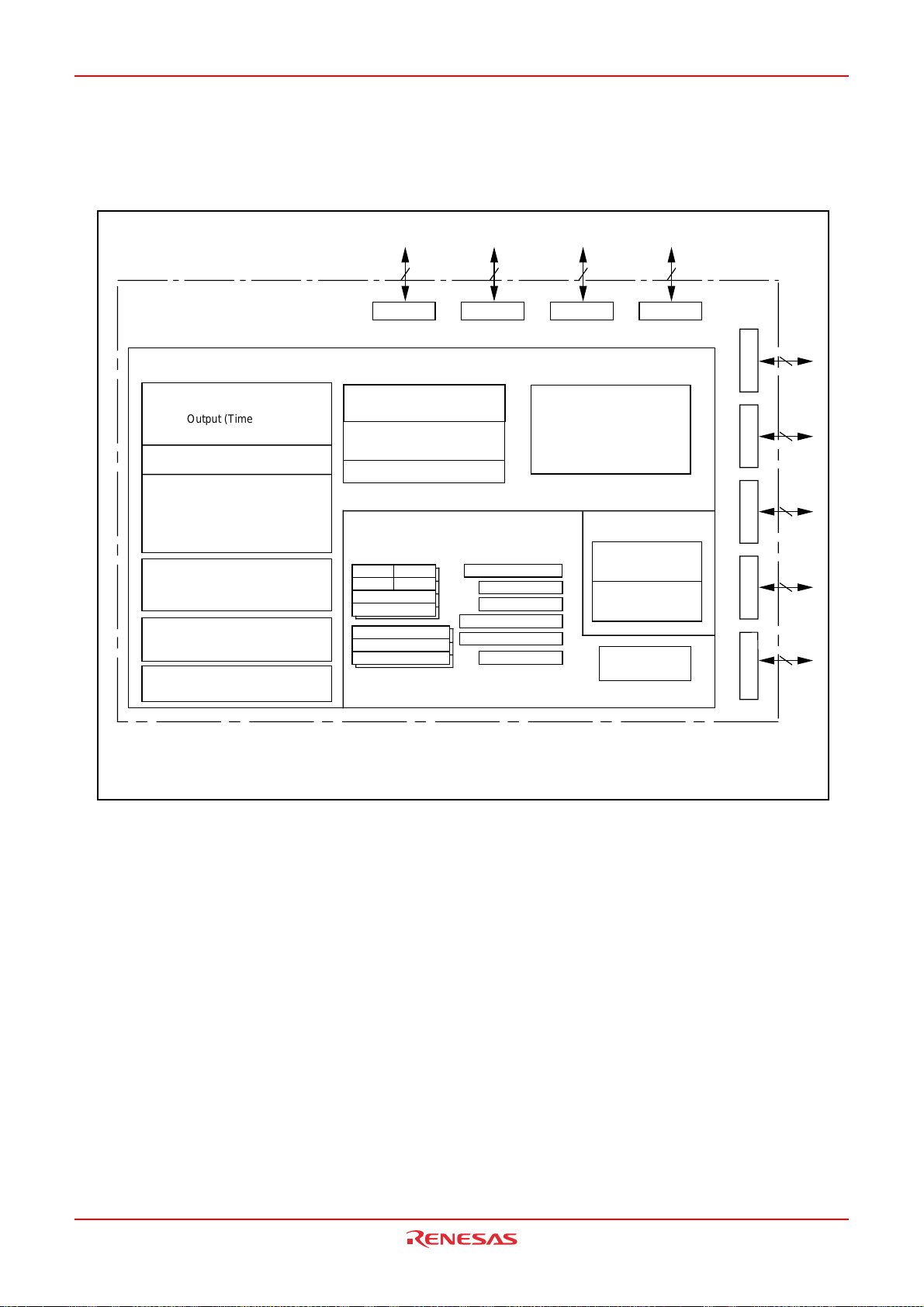
)B82/C61M,82/C61M(puorG82/C61M
A
1.2 Block Diagram
Figure 1.1 is a block diagram of the M16C/28 Group, 80-pin and 85-pin packages.
Figure 1.2 is a block diagram of the M16C/28 Group, 64-pin package.
1. Overview
I/O Ports
Internal Peripheral Functions
Timer (16 bits)
Output (Timer A) : 5
Input (Timer B) : 3
3-phase PWM
Timer S
Input capture/
(
Output compare
Time measurement : 8 channels
Waveform generating : 8 channels
A/D converter
(10 bits x 24 channels)
Watchdog timer
(15 bits)
DMAC
(2 channels)
)
8
Port P0
UART/clock synchronous SI/O
(8 bits x 3 channels)
Clock synchronous SI/O
(8 bits x 2 channels)
Multi-master I2C bus
Port P1
M16C/60 Series CPU Core
R0LR0H
R1H R1L
R2
R3
A0
A1
FB
8
Port P2
System clock generator
On-chip oscillator
PLL frequency synthesizer
SB
USP
ISP
INTB
PC
FLG
8
IN-XOUT
X
XCIN-XCOUT
Memory
ROM
RAM
Multiplier
AA
8
Port P3
(1)
(2)
Port P6
8
Port P7
8
Port P8
8
Port P9
7
Port P10
8
NOTES:
1. ROM size depends on MCU type.
2. RAM size depends on MCU type.
Figure 1.1 M16C/28 Group Block Diagram (80-Pin Package and 85-Pin Package)
page 4
583fo7002,13.naJ00.2.veR
0020-7400B90JER
Page 25
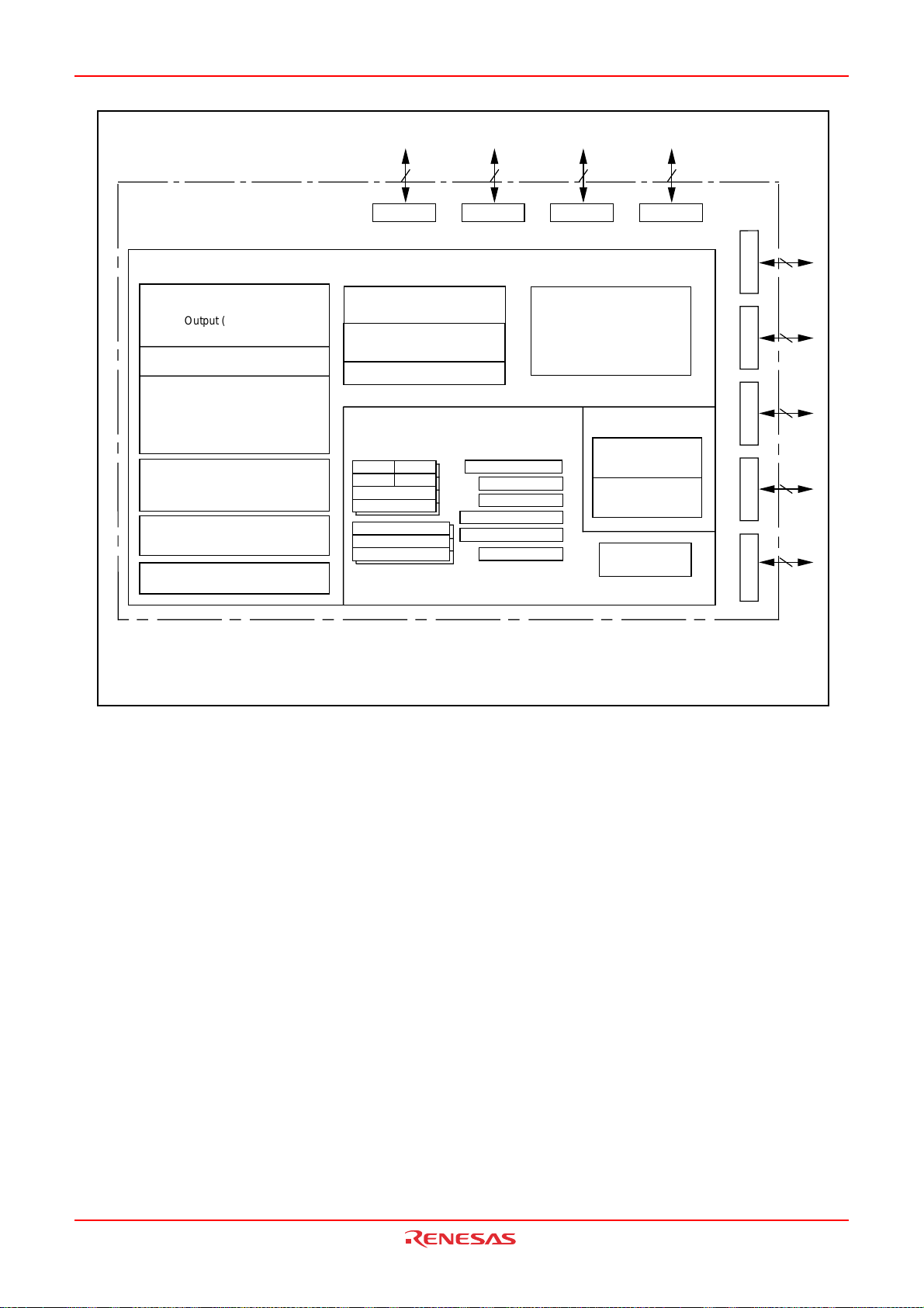
)B82/C61M,82/C61M(puorG82/C61M
1. Overview
I/O Ports
Internal Peripheral Functions
Timer (16 bits)
Output (Timer A) : 5
Input (Timer B) : 3
3-phase PWM
Timer S
Input capture/
(
Output compare
Time measurement : 8 channels
Waveform generating : 8 channels
A/D converter
(10 bits x 13 channels)
Watchdog timer
(15 bits)
DMAC
(2 channels)
)
4
Port P0
UART/Clock synchronous SI/O
(8 bits x 3 channels)
Clock synchronous SI/O
(8 bits x 1 channel)
Multi-master I2C bus
Port P1
M16C/60 Series CPU Core
R0H
R0L
R1H
R1L
R2
R3
A0
A1
FB
3
Port P2
System clock generator
On-chip oscillator
PLL frequency synthesizer
SB
USP
ISP
INTB
PC
FLG
8
X
IN-XOUT
XCIN-XCOUT
Memory
ROM
RAM
Multiplier
4
Port P3
(1)
(2)
Port P6
8
Port P7
8
Port P8
8
Port P9
4
Port P10
8
Figure 1.2 M16C/28 Group Block Diagram (64-Pin Package)
NOTES:
1. ROM size depends on MCU type.
2. RAM size depends on MCU type.
page 5
583fo7002,13.naJ00.2.veR
0020-7400B90JER
Page 26
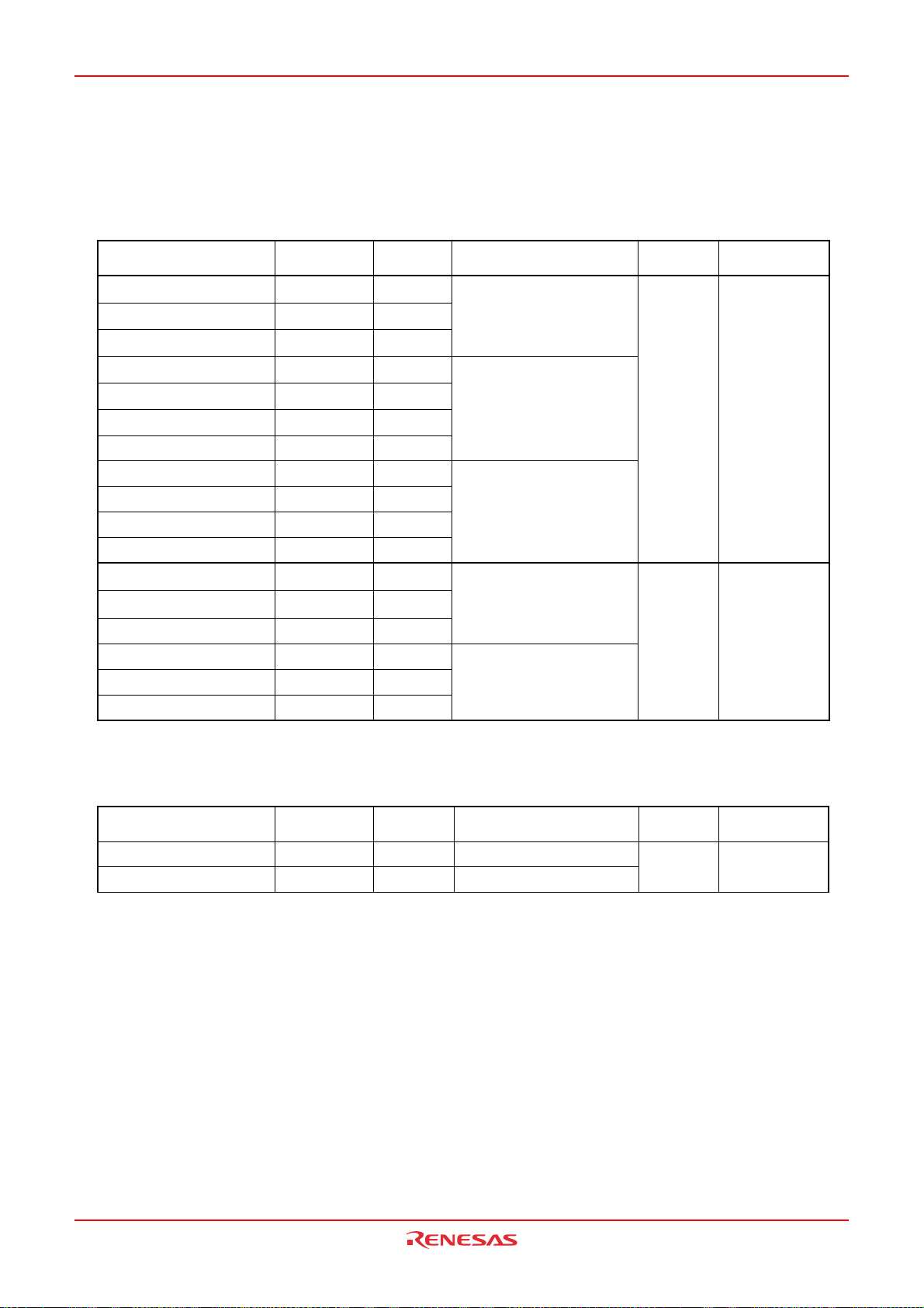
)B82/C61M,82/C61M(puorG82/C61M
1. Overview
1.3 Product Information
Tables 1.3 and 1.4 list the M16C/28 Group product information and Figure 1.3 shows the product number-
ing system. The specifications are partially different between normal-ver.and T/ V-ver..
Table 1.3 M16C/28 Group Product List -Normal-ver. As of January, 2007
rebmuNtraP
GW6F08203M)N(K4+K84K4
MOR
yticapaC
MAR
yticapaC
epyTegakcaPskrameRedoCtcudorP
(N): New
GW8F08203M)N(K4+K46K4
GWAF08203M)N(K4+K69K8
PH6F08203M)N(K4+K84K4
PH8F08203M)N(K4+K46K4
PHAF08203M)N(K4+K69K8
PHCF08203M)N(K4+K821K21
PH6F18203M)N(K4+K84K4
PH8F18203M)N(K4+K46K4
PHAF18203M)N(K4+K69K8
PHCF18203M)N(K4+K821K21
PHXXX-8M08203M)N(K46K4
PHXXX-AM08203M)N(K69K8
PHXXX-CM08203M)N(K821K21
PHXXX-8M18203M)N(K46K4
PHXXX-CM18203M)N(K821K21
)G0F58(A-BJ5800GLTP
)A-Q6P08(A-BK0800PQLP
)A-Q6P46(A-BK4600PQLP
)A-Q6P08(A-BK0800PQLP
)A-Q6P46(A-BK4600PQLPPHXXX-AM18203M)N(K69K8
hsalF
yromeM
ksaM
MOR
9U,7U,5U,3U
5U,3U
Table 1.4 M16C/28B Group Product List -Normal-ver. As of January, 2007
rebmuNtraP
PHBCF08203M)D(K4+K821K21)A-Q6P08(A-BK0800PQLP
PHBCF18203M)D(K4+K821K21)A-Q6P46(A-BK4600PQLP
tnempolevedrednU:)D(
page 6
0020-7400B90JER
MOR
yticapaC
583fo7002,13.naJ00.2.veR
MAR
yticapaC
epyTegakcaPskrameRedoCtcudorP
hsalF
yromem
7U
Page 27

)B82/C61M,82/C61M(puorG82/C61M
Part No. M 3 0 2 8 0 F C B H P - U 7
1. Overview
Product code
Package type:
HP : Package PLQP0080KB-A(80P6Q-A)
PLQP0064KB-A(64P6Q-A)
WG : Package PTLG0085JB-A(85F0G)
Version
(no): M16C/28
B: M16C/28B
ROM capacity / RAM capacity
6 : (48K+4K) bytes / 4K bytes
8 : (64K + 4K) bytes / 4K bytes
A : (96K + 4K) bytes / 8K bytes
C : (128K + 4K) bytes / 12K bytes
Memory type:
F : Flash memory version
M : Mask ROM version
(1)
:
NOTE:
1. "+4K bytes" is available only in flash memory ver..
Figure 1.3 Product Numbering System
Pin count
(The value itself has no specific meaning)
M16C/28 Group
M16C Family
page 7
0020-7400B90JER
583fo7002,13.naJ00.2.veR
Page 28
)B82/C61M,82/C61M(puorG82/C61M
1. Overview
Table 1.5 Product Code (Flash Memory Version) - M16C/28 Normal Version, 64-, 80-, and 85-Pin
Packages
MORlanretnI
tcudorP
edoC
3U
5U Cº58ot027U
9U Cº58ot02-Cº58ot02-
egakcaP
eerfdaeL
dnamargorP
esare
ecnarudne
001
000,1000,01
)5ot0skcolB:ecapSmargorP(
erutarepmeT
egnar
Cº06ot0
dnamargorP
esare
ecnarudne
001Cº06ot0
MORlanretnI
)BdnaAskcolB:ecapSataD(
erutarepmeT
egnar
Cº58ot04-Cº58ot04-
tneibmAgnitarepO
erutarepmeT
Cº58ot04-
NOTE:
1. The lead contained products, D3, D5, D7 and D9, are put together with U3, U5, U7 and U9 respectively.
Lead-free (Sn-Ag-Cu plating) products can be mounted by both conventional Sn-Pb paste and Leadfree paste.
Table 1.6 Product Code (Flash Memory-ver.) - M16C/28B Normal Version, 64- and 80-Pin Package
MORlanretnI
tcudorP
edoC
7Ueerf-daeL000,1Cº06ot0000,01Cº58ot04-Cº58ot04-
egakcaP
margorP
esaredna
ecnarudne
)5ot0skcolB:ecapSmargorP(
margorP
egnarerutarepmeT
esaredna
ecnarudne
MORlanretnI
)BdnaAskcolB:ecapSataD(
erutarepmeT
egnar
tneibmAgnitarepO
erutarepmeT
Table 1.7 Product Code (Mask ROM Version) - M16C/28 Normal Version
tcudorP
edoC
egakcaP
3U
tneibmAgnitarepO
erutarepmeT
Cº58ot04-
eerf-daeL
5UCº58ot02-
page 8
0020-7400B90JER
583fo7002,13.naJ00.2.veR
Page 29
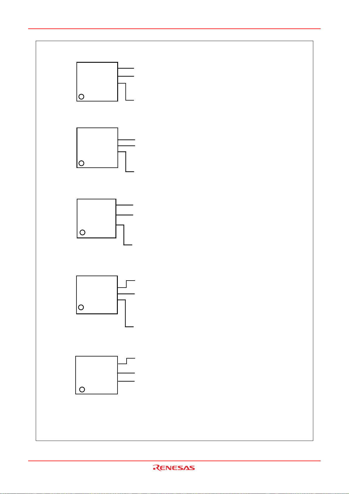
)B82/C61M,82/C61M(puorG82/C61M
(1) Flash Memory Version, PTLG0085JB-A (85F0G), Normal-ver.
1. Overview
M30280FA
B U5
XXXXXXX
(2) Flash Memory Version, PLQP0080KB-A (80P6Q-A), Normal-ver.
Type No. M30280FAWG
Chip version and product code
B : Chip version.
The first edition is shown to be blank and continues with A, B, and C.
U5: Product code. (See Table 1.5)
Date code seven digits
Manufacturing management code
M16C
M30280FAHP
A U5
XXXXXXX
(3) Flash Memory Version, PLQP0064KB-A (64P6Q-A), Normal-ver.
30281FA
A U5
XXXXXXX
Type No. M30280FAHP
Chip version and product code
A : Chip version and product code
The first edition is shown to be blank and continues with A, B and C.
U5 : Product code. (Table 1.5)
Date code seven digits
Manufacturing management code
Type No. M30281FAHP
Chip version and product code
A : Chip version and product code
The first edition is shown to be blank and continues with A, B and C.
U5 : Product code. (Table 1.5)
(1)
(1)
Date code seven digits
Manufacturing management code
(4) Mask ROM Version, PLQP0080KB-A (80P6Q-A), Normal-ver.
M16C
Type No. M30280MAHP
M30280MA-
XXXHP A U5
XXXXXXX
(5) Mask ROM Version, PLQP0064-KB-A (64P6Q-A), Normal-ver.
XXXXXXX
M30281MA-
XXXHP A U5
NOTES:
Chip version and product code
XXX : ROM No.
A : Chip version and product code
The first edition is shown to be blank and continues with A, B and C.
U5 : Product code. (Table 1.7)
Date code seven digits
Manufacturing management code
Date code seven digits
Manufacturing management code
Type No. M30281MAHP
Chip version and product code
XXX: ROM No.
A : Chip version and product code
The first edition is shown to be blank and continues with A, B and C.
U5 : Product code. (Table 1.7)
(1)
(1)
1. The following functinos are not available in the first version and version A products.
-Delay trigger mode 0 of A/D conversion
-Delay trigger mode 1 of A/D conversion
Figure 1.4 Marking Diagram-M16C/28 Group Normal-ver.
page 9
0020-7400B90JER
583fo7002,13.naJ00.2.veR
Page 30
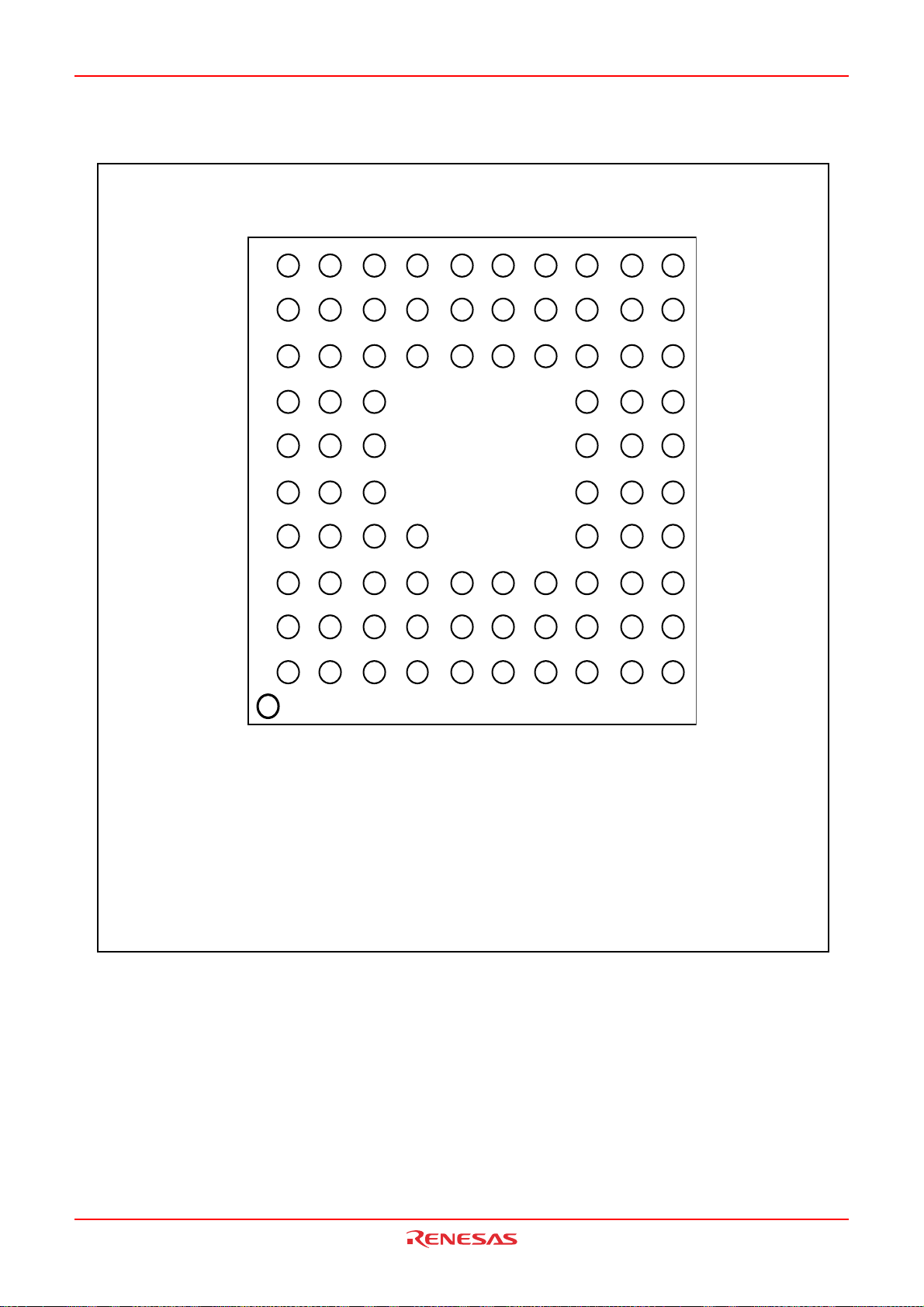
)B82/C61M,82/C61M(puorG82/C61M
T
1.4 Pin Assignment
Figures 1.5 to 1.7 show the pin Assignments (top view).
A
BCDEFG
10
9
8
7
6
5
4
3
2
1
61 60 58
P06 P07 P11
62
63
5
P0
P0
P0
P10
P10
V
64
67
70
74
77
REF
4
P0
P1
65
3
2
P0
P0
68
0
7
P10
P10
71
(11)
5
4 (Vss)
P10
73
1
2
P10
P10
76
0
P10
AVss
78
AVcc79P9
80
P9
1
P9
7
P9
2
6
3
P9
P9
3
5
2
P9
CNVss
5
4
P1
59
5
0
3
P1
66
5
1
2
P1
69
6
(2)
72
3
(11)
75
(2)
(Vss)
4
9
1
RESE
5
7
0
P87/XCIN
6
8
P86/XCOUT
52
7
P1
53
6
P1
54
5 (Vss)
P1
11
Vss14P8
12
IN
X
10
OUT
X
50
1
P2
51
0
P2
(11)
(2)
5
13
Vcc16P8
13
Vcc15P8
1. Overview
H
JK
47
44
42
38
4
7
1
P2
P2
P6
48
45
43
3
P2
49
P2
17
P8
6
P2
P6
46
41
2
5
P2
P6
37
36
2
P3
P3
34
33
5
P3
P3
31
(11)
(2)
P6
(Vss)
29
28
6
P6
P6
26
25
2
1
P7
P7
19
23
3
0
P8
P7
18
21
4
1
P8
P7
1
P3
39
0
0
P3
40
2
3
P6
35
3
4
P3
32
6
7
P3
30
4
5
P6
27
7
0
P7
24
2
3
P7
22
4
5
P7
20
6
7
P7
NOTES:
1. The numbers in each grid (circle) show the pin numbers of the M30280FAHP (PLQP0080KB-A (80P6Q-A))
2. Connect grids written as (Vss) to Vss(GND) or leave them open.
3. Set PACR2 to PACR0 bits in the PACR register to "0112" before you input and output it after resetting to each pin.
When the PACR register is not set, the input and output function of some pins are disabled.
Package: PTLG0085JB-A(85F0G)
Figure 1.5 Pin Assignment (Top View) of 85-pin Package
page 10
583fo7002,13.naJ00.2.veR
0020-7400B90JER
Page 31

)B82/C61M,82/C61M(puorG82/C61M
Table 1.8 Pin Characteristics for 85-Pin Package
niP
.oN
1A9P
2A9P
3AccVA 87
4AV
5A01P
6A01P
7A0P
8A0P
9A0P
01A0P
1B9P
2B9P
3B9P
4B01P
5B01P
6B01P
7B01P
8B0P
9B0P
01B0P
1CssVNC 6
2C9P
3C9P
4CssVA 57
5C01P
6CssV
7C01P
8C0P
9C1P
01C1P
1DX
2DX
3DTESER 9
4DssV
8D1P
9D1P
01D1P
1EX
2EX
3EssV 11
lortnoC
5
6
0
3
5
6
2
3
7
2
4
7
0
1
1
0
1
8P
6
8P
7
2
3
4
troP
1
5IK1
0
2
4IK0
7IK3
3
6IK2
niP
FER
)1(
TUOC
NIC
)1(
TUO
NI
tpurretnI
niP
BT
BT
BT
niPremiTniPSremiTniPTRAU
NI2
NI0
NI1
2
I
KLC
4
S
4TUO
S
4NI
retsam-itluM
niPsubC
NA
NA
NA
NA
NA
NA
NA
NA
niPgolanA
2NA
5
2NA
6
1
5
0NA
0
0NA
3
0NA
5
0NA
6
2NA
4
2NA
7
0
2
4
7
0NA
2
0NA
4
0NA
7
3
6
0NA
1
2NA
0
2NA
1
2NA
2
2NA
3
1. Overview
A-BK0800PQLP
rebmuNniP
1
08
77
47
07
76
46
26
16
3
2
97
67
37
17
86
56
36
06
5
4
27
)11(
96
66
95
85
8
7
)11(
75
65
55
01
21
page 11
583fo7002,13.naJ00.2.veR
0020-7400B90JER
Page 32

)B82/C61M,82/C61M(puorG82/C61M
Table 1.8 Pin Characteristics for 85-Pin Package (continued)
niP
.oN
8E1P
9E1P
01E1P
1FccV 31
2FccV 31
3F8P
8FssV
9F2P
01F2P
1G8P
2G8P
3G8P
8G2P
9G2P
01G2P
1H8P
2H8P
3H7P
4H6P
5HssV
6H3P
7H3P
8H2P
9H2P
01H2P
1J7P
2J7P
3J7P
4J6P
5J6P
6J3P
7J3P
8J6P
9J6P
01J6P
1K7P
2K7P
3K7P
4K7P
5K6P
6K3P
7K3P
8K6P
9K3P
01K3P
lortnoC
niP
)1(
)1(
troP
5
6
7
5
0
1
4
3
2
2
3
4
1
0
1
6
5
2
5
6
7
6
4
2
7
4
6
3
2
0
1
7
5
3
0
5
7
4
3
0
1
tpurretnI
niP
TNI
3
TNI
4
TNI
5
niPremiTniPSremiTniPTRAU
2
I
VDIDA
WDI 35
UDI1CPNI
7
retsam-itluM
niPsubC
GRT
IMNDS 41
1CTUO
0
/
1CPNI
0
1CTUO
1
/
1CPNI
1
TNI
2
PZ 51
TNI
1
TNI
0
1CTUO
2
/
1CPNI
2
1CTUO
3
/
1CPNI
3
1CTUO
4
/
4
1CPNI
AT
NI4
U/ 81
AT
TUO4
U/ 91
AT
NI0
AT
TUO3
AT
TUO2
W/ 32
AT
TUO1
V/KLC2R/XD
AT
NI3
AT
NI2
W/ 22
AT
NI1
V/STC
AT
TUO0
RXD
2
LCS/
2
KLC/
1
RXD
1
S
3TUO
1CTUO
5
/
1CPNI
5
1CTUO
6
/
1CPNI
6
1CTUO
7
/
1CPNI
7
1
TXD
1
STR
1
STC/
1
STC/
0
STC/
0
STR/
2
DXT/
2
STR/
STC/
0
RXD
STR
KLC
TXD2ADS/
STC
KLC
TXD
KLC
S
3NI
SKLC
1
0
0
0
2
1
1
0
3
ADS
MM
LCS
MM
/
1
1
/
SKLC/
1
1. Overview
niPgolanA
A-BK0800PQLP
rebmuNniP
45
25
)11(
15
05
61
71
94
84
74
62
92
)11(
43
73
64
54
44
12
52
82
13
33
63
14
34
24
02
42
72
03
23
53
04
93
83
page 12
583fo7002,13.naJ00.2.veR
0020-7400B90JER
Page 33

7
/AN0
7
P0
0
/AN2
0
P1
1
/AN2
1
P1
2
/AN2
2
P1
3
/AN2
3
P1
)B82/C61M,82/C61M(puorG82/C61M
MM
MM
/SCL
/SDA
2
3
4
5
/INPC1
/INPC1
3
4
/OUTC1
/OUTC1
3
4
P2
P2
6
/INPC1
/INPC1
5
6
/OUTC1
/OUTC1
5
6
P2
P2
7
0
/INPC1
7
/RTS
0
/CTS
/OUTC1
0
7
P6
P2
0
/CLK
1
P6
0
/RxD
2
P6
1
0
/IDU
/IDV
7
/INPC1
/INPC1
/INPC1
TRG
/AD
/IDW
3
4
/INT
/INT
4
5
6
P1
P1
P1
0
/INPC1
5
/INT
/OUTC1
7
0
P1
P2
2
1
/OUTC1
/OUTC1
2
1
P2
P2
1. Overview
56
P06/AN0
P05/AN0
P04/AN0
P03/AN0
P02/AN0
P01/AN0
P00/AN0
P107/AN7/KI
P106/AN6/KI
P105/AN5/KI
P104/AN4/KI
P103/AN
P102/AN
P101/AN
AV
SS
P100/AN
V
REF
AVcc
P97/AN27/SIN
P96/AN26/SOUT
NOTES:
1.Set PACR2 to PACR0 bit in the PACR register to "011
input and output it after resetting to each pin. When the PACR
register isn't set up, the input and output function of some of the pins
are disabled.
61
6
62
5
63
4
64
3
65
2
66
1
67
0
68
3
69
2
70
1
71
0
3
72
PLQP0080KB-A (80P6Q-A)
73
2
74
1
75
76
0
77
78
79
4
80
4
1 2 3 4 5 6 7 8 91011121314151617181920
4
4
/CLK
/AN2
5
3
P9
/AN2
5
P9
M16C/28 Group
(M16C/28, M16C/28B)
(Top View)
IN
IN
IN
CIN
COUT
/X
/TB1
1
P9
/TB0
0
P9
7
CNVss
P8
/X
6
P8
/TB2
2
P9
SS
OUT
V
X
RESET
2
" before you
41424344454647484950515253545557585960
40
39
38
37
36
35
34
33
32
31
30
29
28
27
26
25
24
23
22
21
1
/ZP
2
/NMI/SD
/INT
5
4
P8
P8
/INT
3
P8
0
/INT
2
P8
/U
IN
/TA4
1
P8
/U
OUT
/TA4
0
P8
IN
/TA3
7
P7
IN
CC
X
V
P63/TXD
0
P3
0
/CLK
3
P31/SIN
3
P32/SOUT
3
P3
3
P3
4
P3
5
P3
6
P3
7
P64/CTS1/RTS1/CTS0/CLKS
5
/CLK
1
P6
P66/RxD
1
P67/TXD
1
P70/TXD2/SDA2/TA0
OUT
/CTS1/RTS1/CTS0/CLKS
P71/RXD2/SCL2/TA0IN/CLK1
2
/CLK2/TA1
OUT
OUT
OUT
/V/RxD1
/W
P7
3
/CTS2/RTS2/TA1IN/V/TxD1
P7
P74/TA2
P75/TA2IN/W
P76/TA3
1
1
Figure 1.6 Pin Assignment (Top View) of 80-Pin Package
page 13
0020-7400B90JER
583fo7002,13.naJ00.2.veR
Page 34

)B82/C61M,82/C61M(puorG82/C61M
Table 1.9 Pin Characteristics for 80-Pin Package
niP
.oN
19P
29P
39P
49P
59P
6ssVNC
7X
8X
9TESER
01X
11ssV
21X
31ccV
418P
518P
618P
718P
818P
918P
027P
127P
227P
327P
427P
527P
627P
727P
826P
926P
036P
136P
233P
333P
433P
533P
633P
733P
833P
933P
046P
lortnoC
niP
NIC
TUOC
TUO
NI
troP
5
3
2
1
0
8P
7
8P
6
5
4
3
2
1
0
7
6
5
4
3
2
1
0
7
6
5
4
7
6
5
4
3
2
1
0
3
niP
IMNDS
TNI
2
TNI
1
TNI
0
tpurretnI
BT
BT
BT
niPremiTniPSremiTniPTRAU
NI2
NI1
NI0
PZ
AT
NI4
U/
AT
TUO4
U/
AT
NI3
AT
TUO3
AT
NI2
W/
AT
TUO2
W/
AT
NI1
V/STC
AT
TUO1
V/KLC
AT
NI0
AT
TUO0
RXD
TXD
TXD
RXD
S
S
TXD
KLC
4
2
2R/XD1
2
2
1
STC
1
1
KLC
1
STR
1
1
SKLC
3TUO
3NI
KLC
3
0
STR/
2T/XD1
LCS/
2
ADS/
2
STC/
0
STC/
1
1. Overview
2
I
KLC/
1
STR/
1
/
SKLC/
1
STC/
0
/
retsam-itluM
niPsubC
niPgolanA
2NA
5
2NA
4
page 14
583fo7002,13.naJ00.2.veR
0020-7400B90JER
Page 35

)B82/C61M,82/C61M(puorG82/C61M
Table 1.9 Pin Characteristics for 80-Pin Package (continued)
niP
.oN
146P
246P
346P
442P
542P
642P
742P
842P
942P
052P
152P
251P
351P
451P
551P
651P
751P
851P
951P
060P
160P
260P
360P
460P
560P
660P
760P
8601P
9601P
0701P
1701P
2701P
3701P
4701P
57ssVA
6701P
77V
87ccVA
979P
089P
lortnoC
niP
FER
troP
2
1
0
7
6
5
4
3
2
1
0
7
6
5
4
3
2
1
0
7
6
5
4
3
2
1
0
7IK3
6IK2
5IK1
4IK0
3
2
1
0
7
6
tpurretnI
niP
niPremiTniPSremiTniPTRAU
RXD
1CTUO
7
1CTUO
6
1CTUO
5
1CTUO
4
1CTUO
3
1CTUO
2
1CTUO
1
1CTUO
0
TNI
5
TNI
4
TNI
3
UDI1CPNI
7
WDI
VDIDA
1CPNI/
7
1CPNI/
6
1CPNI/
5
1CPNI/
4
1CPNI/
3
1CPNI/
2
1CPNI/
1
1CPNI/
0
S
S
1. Overview
2
I
0
KLC
0
STR
0
STC/
0
LCS
ADS
retsam-itluM
niPsubC
MM
MM
NA
NA
NA
NA
NA
NA
NA
NA
4NI
4TUO
niPgolanA
GRT
2NA
3
2NA
2
2NA
1
2NA
0
0NA
7
0NA
6
0NA
5
0NA
4
0NA
3
0NA
2
0NA
1
0NA
0
7
6
5
4
3
2
1
0
2NA
7
2NA
6
page 15
583fo7002,13.naJ00.2.veR
0020-7400B90JER
Page 36

3
/AN0
3
P0
/IDV
TRG
/AD
3
/INT
5
P1
/IDW
4
/INT
6
P1
MM
/SDA
0
/IDU
7
/INPC1
0
/INPC1
5
/OUTC1
/INT
0
7
P2
P1
)B82/C61M,82/C61M(puorG82/C61M
MM
/SCL
1
2
/INPC1
/INPC1
1
2
/OUTC1
/OUTC1
1
2
P2
P2
4
3
/INPC1
/INPC1
4
3
/OUTC1
/OUTC1
4
3
P2
P2
5
6
/INPC1
/INPC1
5
6
/OUTC1
/OUTC1
5
6
P2
P2
7
0
/INPC1
7
/RTS
0
/CTS
/OUTC1
0
7
P6
P2
0
/CLK
1
P6
0
/RxD
2
P6
0
/TxD
3
P6
1. Overview
P02/AN0
P01/AN0
P00/AN0
P107/AN7/KI
P106/AN6/KI
P105/AN5/KI
P104/AN4/KI
P103/AN
P102/AN
P101/AN
AV
P100/AN
V
REF
AV
P93/AN2
P92/TB2
44
45
46
47
48
2
49
50
1
0
51
3
52
53
2
1
54
0
55
3
56
2
57
1
58
SS
59
0
60
(M16C/28, M16C/28B)
PLQP0064KB-A (64P6Q-A)
42
43
39
40
41
M16C/28 Group
(Top View)
36
37
38
61
CC
IN
62
4
63
64
2
IN
/TB0
0
P9
3
SS
CNV
4
CIN
/X
7
P8
5
COUT
/X
6
P8
7
6
OUT
X
RESET
9
8
IN
SS
X
V
10
CC
V
12
11
/ZP
2
/NMI/SD
/INT
5
4
P8
P8
13
1
/INT
3
P8
1
IN
/TB1
1
P9
35
14
0
/INT
2
P8
34
15
/U
IN
/TA4
1
P8
33
16
/U
OUT
/TA4
0
P8
32
31
30
29
28
27
26
25
24
23
22
21
20
19
18
17
P30/CLK
3
P31/S
IN3
P32/S
OUT3
P3
3
P64/CTS1/RTS1/CTS0/CLKS1
5
/CLK
1
P6
P66/RxD
1
P67/TxD
1
P70/TxD2/SDA2/TA0
1
/RxD2/SCL2/TA0IN/CLK1
P7
2
/CLK2/TA1
P7
3
/CTS2/RTS2/TA1IN/V/TxD1
P7
P74/TA2
OUT
P7
5
/TA2IN/W
6
/TA3
OUT
P7
P77/TA3
IN
OUT
/RTS1/CTS1/CTS0/CLKS1
OUT
/V/RxD1
/W
NOTES:
1.Set PACR2 to PACR0 bit in the PACR register to "010
2
" before you
input and output it after resetting to each pin. When the PACR
register isn't set up, the input and output function of some of the pins
are disabled.
Figure 1.7 Pin Assignment (Top View) of 64-Pin Package
page 16
0020-7400B90JER
583fo7002,13.naJ00.2.veR
Page 37

)B82/C61M,82/C61M(puorG82/C61M
Table 1.10 Pin Characteristics for 64-Pin Package
niP
.oN
19P
29P
3ssVNC
4X
5X
6TESER
7X
8ssV
9X
01ccV
118P
218P
318P
418P
518P
618P
717P
817P
917P
027P
127P
227P
327P
427P
526P
626P
726P
826P
923P
033P
133P
233P
336P
436P
536P
636P
732P
832P
932P
042P
lortnoC
niP
NIC
TUOC
TUO
NI
troP
1
0
8P
7
8P
6
5
4
3
2
1
0
7
6
5
4
3
2
1
0
7
6
5
4
3
2
1
0
3
2
1
0
7
6
5
4
niP
IMNDS
TNI
2
TNI
1
TNI
0
tpurretnI
AT
BT
niPremiTniPSremiTniPTRAU
NI1
NI0
PZ
AT
NI4
U/
AT
TUO4
U/
AT
NI3
AT
TUO3
AT
NI2
W/
AT
TUO2
W/
AT
NI1
V/STC
AT
TUO1
V/KLC
AT
NI0
AT
TUO0
1CTUO
7
1CTUO
6
1CTUO
5
1CTUO
4
1. Overview
2
I
2
STR/
2T/XD1
2R/XD1
RXD
2
LCS/
2
KLC/
1
TXD
2
ADS/
2
STR/
1
/
1
STC/
0
SKLC/
STC
TXD
1
RXD
1
KLC
1
STR
1
STC/
1
SKLC
1
S
3TUO
S
3NI
KLC
3
TXD
0
RXD
0
KLC
0
STR
0
STC/
0
1CPNI/
7
1CPNI/
6
1CPNI/
5
1CPNI/
4
1
STC/
0
/
retsam-tluM
niPsubC
niPgolanA
page 17
583fo7002,13.naJ00.2.veR
0020-7400B90JER
Page 38

)B82/C61M,82/C61M(puorG82/C61M
Table 1.10 Pin Characteristics for 64-Pin Package (continued)
niP
.oN
142P
242P
342P
442P
541P
641P
741P
840P
940P
050P
150P
2501P
3501P
4501P
5501P
6501P
7501P
8501P
95ssVA
0601P
16V
26ccVA
369P
469P
lortnoC
niP
FER
troP
3
2
1
0
7
6
5
3
2
1
0
7IK3
6IK2
5IK1
4IK0
3
2
1
0
3
2
tpurretnI
niP
TNI
5
TNI
4
TNI
3
UDI1CPNI
WDI
VDIDA
BT
niPremiTniPSremiTniPTRAU
1CTUO
3
1CTUO
2
1CTUO
1
1CTUO
0
7
NI2
1CPNI/
3
1CPNI/
2
1CPNI/
1
1CPNI/
0
1. Overview
2
I
LCS
ADS
retsam-itluM
niPsubC
MM
MM
NA
NA
NA
NA
NA
NA
NA
NA
niPgolanA
GRT
0NA
3
0NA
2
0NA
1
0NA
0
7
6
5
4
3
2
1
0
2NA
4
page 18
583fo7002,13.naJ00.2.veR
0020-7400B90JER
Page 39
)B82/C61M,82/C61M(puorG82/C61M
1.5 Pin Description
Table 1.11 Pin Description (64-pin, 80-pin and 85-pin packages)
Classification Symbol I/O Type Function
Power Supply
Analog Power
Supply
Reset Input
CNVSS
Main Clock
Input
Main Clock
Output
Sub Clock Input
Sub Clock Output
______
INT Interrupt
Input
_______
NMI Interrupt
Input
Key Input Interrupt
Timer A
Timer B
Three-phase
Motor Control
Timer Output
Serial I/O
I2C bus Mode
Multi-master
I2C bus
Reference
Voltage Input
A/D Converter
I : Input O : Output I/O : Input and output
VCC, VSS
AVCC
AVSS
____________
RESET
CNVSS
XIN
XOUT
XCIN
XCOUT
________ ________
INT0 to INT5
_______
NMI
_____ _____
KI0 to KI3
TA0OUT to
TA4OUT
TA0IN to
TA4IN
ZP
IN to
TB0
TB2IN
___ ___
U, U, V, V,
___
W, W
IDU, IDW,
_____
IDV, SD
_________ _________
CTS0 to CTS2
_________ _________
RTS0 to RTS2
CLK0 to CLK3
RxD0 to RxD2
TxD0 to TxD2
CLKS1
SDA2
SCL2
SDAMM
SCLMM
VREF
AN0 to AN7
AN00 to AN0
AN2
___________
ADTRG
3
4
O
O
I/O
O
I/O
O
I/O
O
O
I/O
I/O
I
I
I
Apply 2.7 to 5.5V to the Vcc pin. Apply 0V to the Vss pin.
I
Supplies power to the A/D converter. Connect the AV
the AVSS pin to VSS.
I
The microcomputer is in a reset state when "L" is applied to the RESET pin
I
Connect the CNVSS pin to VSS.
I/O pins for the main clock oscillation circuit. Connect a ceramic resonator
I
or crystal oscillator between XIN and XOUT. To apply external clock, apply
IN and leave XOUT open. If XIN is not used (for external oscillator or
it to X
external clock) connect XIN pin to VCC and leave XOUT open.
I/O pins for the sub clock oscillation circuit. Connect a crystal oscillator
I
between XCIN and XCOUT.
Input pins for the INT interrupt. INT2 can be used for Timer A Z-phase
I
function.
Input pin for the NMI interrupt. NMI cannot be used as I/O port while the three-
I
______ ________
_______ _______
phase motor control is enabled. Apply a stable "H" to NMI after setting it's
direction register to "0" when the three-phase motor control is enabled.
Input pins for the key input interrupt
I
I/O pins for the timer A0 to A4
Input pins for the timer A0 to A4
I
Input pin for Z-phase
I
Input pins for the timer B0 to B2
I
Output pins for the three-phase motor control timer
Input and output pins for the three-phase motor control timer
Input pins for data transmission control
I
Output pins for data reception control
Inputs and outputs the transfer clock
Inputs serial data
I
Outputs serial data
Output pin for transfer clock
Inputs and outputs serial data
Inputs and outputs the transfer clock
Inputs and outputs serial data
Inputs and outputs the transfer clock
Applies reference voltage to the A/D converter
Analog input pins for the A/D converter
Input pin for an external A/D trigger
1. Overview
CC pin to VCC and
___________
_______
page 19
583fo7002,13.naJ00.2.veR
0020-7400B90JER
Page 40

)B82/C61M,82/C61M(puorG82/C61M
Table 1.11 Pin Description (64-pin, 80-pin and 85-pin packages) (Continued)
Classification Symbol I/O Type Function
Timer S
I/O Ports
INPC10 to INPC17
OUTC10 to OUTC1
P00 to P03
P15 to P17
P20 to P27
P30 to P33
P60 to P67
P70 to P77
P80 to P87
P90 to P93
P100 to P10
7
7
I
O
I/O
Input pins for the time measurement function
Output pins for the waveform generating function
CMOS I/O ports which have a direction register determines an individual
pin is used as an input port or an output port. A pull-up resistor is selectable for every 4 input ports.
I : Input O : Output I/O : Input and output
1. Overview
page 20
0020-7400B90JER
583fo7002,13.naJ00.2.veR
Page 41

)B82/C61M,82/C61M(puorG82/C61M
Table 1.11 Pin Description (80-pin and 85-pin packages only) (Continued)
Classification Symbol I/O Type Function
Serial I/O
A/D Converter
I/O Ports
CLK4
SIN4
SOUT4
AN04 to AN0
AN20 to AN2
AN25 to AN2
P04 to P07
P10 to P14
P34 to P37
I/O
7
3
7
I/O
Inputs and outputs the transfer clock
Inputs serial data
I
Outputs serial data
O
Analog input pins for the A/D converter
I
CMOS I/O ports which have a direction register determines an individual
pin is used as an input port or an output port. A pull-up resistor is selectable for every 4 input ports.
P95 to P97
I : Input O : Output I/O : Input and output
1. Overview
page 21
583fo7002,13.naJ00.2.veR
0020-7400B90JER
Page 42

)B82/C61M,82/C61M(puorG82/C61M
b15
b0
b7
b8
b
2. Central Processing Unit(CPU)
2. Central Processing Unit (CPU)
Figure 2.1 shows the CPU registers. The register bank is comprised of 7 registers (R0, R1, R2, R3, A0, A1
and FB) out of 13 CPU registers. Two sets of register banks are provided.
b31
b19
b15
R0H(R0's high bits)
R1H(R1's high bits)
b15
R2
R3
INTBH
The upper 4 bits of INTB are INTBH and
the lower 16 bits of INTB are INTBL.
b19
b15
b15
b8 b7 b0
R0L(R0's low bits)
R1L(R1's low bits)
R2
R3
A0
A1
FB
INTBL
PC
US P
ISP
SB
FLG
b0
b0
b0
b0
Data registers
Address registers
Frame base registers
Interrupt table register
Program counter
User stack pointer
Interrupt stack pointer
Static base register
Flag register
Carry flag
Debug flag
Zero flag
Sign flag
Register bank select flag
Overflow flag
Interrupt enable flag
Stack pointer select flag
Reserved space
Processor interrupt priority level
Reserved space
(1)
(1)
(1)
NOTES:
1. The register bank is comprised of these registers. Two sets of register banks are provided.
Figure 2.1 Central Processing Unit Register
2.1 Data Registers (R0, R1, R2 and R3)
The R0, R1, R2 and R3 registers are 16 bit registers for transfer and arithmetic/logic operations.
The R0 and R1 registers can be split into high-order bits(R0H, R1H) and low-order bits (R0L, R1L) to be
used seperately as 8-bit data registers. Conversely, R2 and R0 can be combined with R2 to be used as a
32-bit data register (R2R0). The same applies to R1 and R2.
2.2 Address Registers (A0 and A1)
The register A0 consists of 16 bits, and is used for address register indirect addressing and address register
relative addressing. They also are used for transfers and arithmetic/logic operations. A1 is the same as A0.
In some instructions, registers A1 and A0 can be combined for use as a 32-bit address register (A1A0).
page 22
0020-7400B90JER
583fo7002,13.naJ00.2.veR
Page 43

)B82/C61M,82/C61M(puorG82/C61M
2. Central Processing Unit(CPU)
2.3 Frame Base Register (FB)
FB is configured with 16 bits, and is used for FB relative addressing.
2.4 Interrupt Table Register (INTB)
INTB is configured with 20 bits, indicating the start address of an interrupt vector table.
2.5 Program Counter (PC)
PC is configured with 20 bits, indicating the address of an instruction to be executed.
2.6 User Stack Pointer (USP) and Interrupt Stack Pointer (ISP)
Stack pointer (SP) comes in two types: USP and ISP, each configured with 16 bits.
Your desired type of stack pointer (USP or ISP) can be selected by the U flag of FLG.
2.7 Static Base Register (SB)
SB is configured with 16 bits, and is used for SB relative addressing.
2.8 Flag Register (FLG)
FLG consists of 11 bits, indicating the CPU status.
2.8.1 Carry Flag (C Flag)
This flag retains a carry, borrow, or shift-out bit that has occurred in the arithmetic/logic unit.
2.8.2 Debug Flag (D Flag)
The D flag is used exclusively for debugging purpose. During normal use, it must be set to “0”.
2.8.3 Zero Flag (Z Flag)
This flag is set to “1” when an arithmetic operation resulted in 0; otherwise, it is “0”.
2.8.4 Sign Flag (S Flag)
This flag is set to “1” when an arithmetic operation resulted in a negative value; otherwise, it is “0”.
2.8.5 Register Bank Select Flag (B Flag)
Register bank 0 is selected when this flag is “0” ; register bank 1 is selected when this flag is “1”.
2.8.6 Overflow Flag (O Flag)
This flag is set to “1” when the operation resulted in an overflow; otherwise, it is “0”.
2.8.7 Interrupt Enable Flag (I Flag)
This flag enables a maskable interrupt.
Maskable interrupts are disabled when the I flag is “0”, and are enabled when the I flag is “1”. The I flag
is cleared to “0” when the interrupt request is accepted.
2.8.8 Stack Pointer Select Flag (U Flag)
ISP is selected when the U flag is “0”; USP is selected when the U flag is “1”.
The U flag is cleared to “0” when a hardware interrupt request is accepted or an INT instruction for
software interrupt Nos. 0 to 31 is executed.
2.8.9 Processor Interrupt Priority Level (IPL)
IPL is configured with three bits, for specification of up to eight processor interrupt priority levels from level
0 to level 7.
If a requested interrupt has priority greater than IPL, the interrupt is enabled.
2.8.10 Reserved Area
When write to this bit, write "0". When read, its content is undefined.
page 23
0020-7400B90JER
583fo7002,13.naJ00.2.veR
Page 44

)B82/C61M,82/C61M(puorG82/C61M
3. Memory
Figure 3.1 is a memory map of the M16C/28 Group. M16C/28 Group provides 1-Mbyte address space from
addresses 0000016 to FFFFF16. The internal ROM is allocated lower addresses beginning with address
FFFFF16. For example, 64 Kbytes internal ROM is allocated addresses F000016 to FFFFF16.
Two 2-Kbyte internal ROM areas, block A and block B, are available in the flash memory version. The
blocks are allocated addresses F00016 to FFFF16.
The fixed interrupt vector tables are allocated addresses FFFDC16 to FFFFF16. It stores the starting address of each interrupt routine. See the section on interrupts for details.
The internal RAM is allocated higher addresses beginning with address 0040016. For example, 4-Kbytes
internal RAM is allocated addresses 0040016 to 013FF16. Besides storing data, it becomes stacks when the
subroutine is called or an interrupt is acknowledged.
SFR, consisting of control registers for peripheral functions such as I/O port, A/D converter, serial I/O,
timers is allocated addresses 0000016 to 003FF16. All blank spaces within SFR are reserved and cannot be
accessed by users.
The special page vector table is allocated to the addresses FFE0016 to FFFDB16. This vector is used by the
JMPS or JSRS instruction. For details, refer to the
M16C/60 and M16C/20 Series Software Manual
3. Memory
.
Internal RAM area
Memory size
4K bytes
00000
16
SFR Area
00400
16
Internal RAM Area
FFE00
XXXXX
16
RESERVED
0F000
16
Internal ROM Area
0FFFF
YYYYY
FFFFF
(data space)
16
RESERVED
16
Internal ROM Area
(program space)
16
(1)
FFFDC
FFFFF
6K bytes
8K bytes
12K bytes
16
Special Page
Vector Table
16
Undefined Instruction
Overflow
BRK Instruction
Address Match
Single Step
Watchdog Timer
16
Reset
DBC
NMI
XXXXX
013FF
01AFF
023FF
033FF
16
16
16
16
16
Internal ROM area
Memory size
48K bytes
64K bytes
96K bytes
128K bytes
YYYYY
F4000
F0000
E8000
E0000
16
16
16
16
16
NOTES:
1. The block A (2K bytes) and block B (2K bytes) are shown (only flash memory).
2. Do not write to the internal ROM area in Mask ROM ver..
Figure 3.1 Memory Map
page 24
0020-7400B90JER
583fo7002,13.naJ00.2.veR
Page 45

)B82/C61M,82/C61M(puorG82/C61M
4. Special Function Register (SFR)
4. Special Function Register (SFR)
SFR (Special Function Register) is the control register of peripheral functions. Tables 4.1 to 4.7 list the SFR
information.
Table 4.1 SFR Information(1)
Address
0000
16
0001
16
0002
16
0003
16
0004
16
Processor mode register 0 PM0 0016
0005
16
Processor mode register 1 PM1 000010002
0006
16
System clock control register 0 CM0 010010002
0007
16
System clock control register 1 CM1 001000002
0008
16
0009
16
Address match interrupt enable register AIER XXXXXX002
000A
16
Protect register PRCR XX0000002
000B
16
000C
16
Oscillation stop detection register
000D
16
000E
16
Watchdog timer start register WDTS XX16
000F
16
Watchdog timer control register WDC 00XXXXXX2
0010
16
Address match interrupt register 0 RMAD0 0016
0011
16
0012
16
0013
16
0014
16
Address match interrupt register 1 RMAD1 0016
0015
16
0016
16
0017
16
0018
16
0019
16
Voltage detection register 1
001A
16
Voltage detection register 2
001B
16
001C
16
PLL control register 0 PLC0 0001X0102
001D
16
001E
16
Processor mode register 2 PM2 XXX000002
001F
16
Low voltage detection interrupt register D4INT 0016
0020
16
DMA0 source pointer SAR0 XX16
0021
16
0022
16
0023
16
0024
16
DMA0 destination pointer DAR0 XX16
0025
16
0026
16
0027
16
0028
16
DMA0 transfer counter TCR0 XX16
0029
16
002A
16
002B
16
002C
16
DMA0 control register DM0CON 00000X002
002D
16
002E
16
002F
16
0030
16
DMA1 source pointer SAR1 XX16
0031
16
0032
16
0033
16
0034
16
DMA1 destination pointer DAR1 XX16
0035
16
0036
16
0037
16
0038
16
DMA1 transfer counter TCR1 XX16
0039
16
003A
16
003B
16
003C
16
DMA1 control register DM1CON 00000X002
003D
16
003E
16
003F
16
NOTES:
1.The blank spaces are reserved. No access is allowed.
2. The CM20, CM21, and CM27 bits do not change at oscillation stop detection reset.
3. This register does not change at software reset, watchdog timer reset and oscillation stop detection reset.
X : Indeterminate
(1)
Register Symbol After Reset
(2)
CM2 0X0000102
0016
X016
0016
X016
(3)
(3)
VCR1 000010002
VCR2 0016
XX16
XX16
XX16
XX16
XX16
XX16
XX16
XX16
XX16
XX16
page 25
583fo7002,13.naJ00.2.veR
0020-7400B90JER
Page 46

)B82/C61M,82/C61M(puorG82/C61M
4. Special Function Register (SFR)
Table 4.2 SFR Information(2)
Address
0040
16
0041
16
0042
16
0043
16
0044
16
0045
0046
0047
0048
0049
004A
004B
004C
004D
004E
004F
0050
0051
0052
0053
0054
0055
0056
0057
0058
0059
005A
005B
005C
005D
005E
005F
0060
0061
0062
0063
0064
0065
0066
0067
0068
0069
006A
006B
006C
006D
006E
006F
0070
0071
0072
0073
0074
0075
0076
0077
0078
0079
007A
007B
007C
007D
007E
007F
INT3 interrupt control register INT3IC XX00X000
16
IC/OC 0 interrupt control register ICOC0IC XXXXX000
16
IC/OC
1 interrupt control register, I2C bus interface interrupt control register
IC/OC
16
16
16
16
16
16
16
16
16
16
16
16
16
16
16
16
16
16
16
16
16
16
16
16
16
16
16
16
16
16
16
16
16
16
16
16
16
16
16
16
16
16
16
16
16
16
16
16
16
16
16
16
16
16
16
16
16
base timer interrupt control register, SCLSDA interrupt control register BTIC, SCLDAIC
SI/O4 interrupt control register, INT5 interrupt control register S4IC, INT5IC XX00X000
SI/O3 interrupt control register, INT4 interrupt control register S3IC, INT4IC XX00X000
UART2 Bus collision detection interrupt control register BCNIC XXXXX000
DMA0 interrupt control register DM0IC XXXXX000
DMA1 interrupt control register DM1IC XXXXX000
Key input interrupt control register KUPIC XXXXX000
A/D conversion interrupt control register ADIC XXXXX000
UART2 transmit interrupt control register S2TIC XXXXX000
UART2 receive interrupt control register S2RIC XXXXX000
UART0 transmit interrupt control register S0TIC XXXXX000
UART0 receive interrupt control register S0RIC XXXXX000
UART1 transmit interrupt control register S1TIC XXXXX000
UART1 receive interrupt control register S1RIC XXXXX000
Timer A0 interrupt control register TA0IC XXXXX000
Timer A1 interrupt control register TA1IC XXXXX000
Timer A2 interrupt control register TA2IC XXXXX000
Timer A3 interrupt control register TA3IC XXXXX000
Timer A4 interrupt control register TA4IC XXXXX000
Timer B0 interrupt control register TB0IC XXXXX000
Timer B1 interrupt control register TB1IC XXXXX000
Timer B2 interrupt control register TB2IC XXXXX000
INT0 interrupt control register INT0IC XX00X000
INT1 interrupt control register INT1IC XX00X000
INT2 interrupt control register INT2IC XX00X000
(1)
Register
Note 1: The blank spaces are reserved. No access is allowed.
Symbol
After Reset
I COC1 I C , I I C I C XXXXX000
XXXXX000
2
2
2
2
2
2
2
2
2
2
2
2
2
2
2
2
2
2
2
2
2
2
2
2
2
2
2
2
X : Indeterminate
page 26
583fo7002,13.naJ00.2.veR
0020-7400B90JER
Page 47

)B82/C61M,82/C61M(puorG82/C61M
4. Special Function Register (SFR)
Table 4.3 SFR Information(3)
Address
~
~
01B0
16
01B1
16
01B2
16
01B3
16
Flash memory control register 4
01B4
16
01B5
16
Flash memory control register 1
01B6
16
01B7
16
Flash memory control register 0
01B8
16
01B9
16
~
~
0210
16
Low-power Consumption Control 0 LPCC0 X0000001
0211
16
0212
16
0213
16
0214
16
0215
16
0216
16
0217
16
0218
16
0219
16
~
~
0250
16
0251
16
0252
16
0253
16
0254
16
0255
16
0256
16
0257
16
0258
16
0259
16
025A
16
025B
16
025C
16
On-chip oscillator control register ROCR X0000101
025D
16
Pin assignment control register PACR 00
025E
16
Peripheral clock select register PCLKR 00000011
025F
16
Low-power Consumption Control 1 LPCC1 00
(1)
Register Symbol After Reset
(2)
(2)
FMR1 000XXX0X
(2)
FMR4 01000000
FMR0 00000001
16
16
2
2
2
2
2
2
~
~
~
~
~
~
~
~
02E0
16
I2C0 data shift register S00 XX
02E1
16
02E2
16
I2C0 address register S0D0 00
02E3
16
I2C0 control register 0 S1D0 00
02E4
16
I2C0 clock control register S20 00
02E5
16
I2C0 start/stop condition control register S2D0 00011010
02E6
16
I2C0 control register 1 S3D0 00110000
02E7
16
I2C0 control register 2 S4D0 00
02E8
16
I2C0 status register S10 0001000X
02E9
16
02EA
16
~
~
02FE
16
02FF
16
Note 1:The blank spaces are reserved. No access is allowed.
Note 2:This register is included in the flash memory version.
X : Indeterminate
page 27
583fo7002,13.naJ00.2.veR
0020-7400B90JER
~
~
16
16
16
16
2
2
16
2
~
~
Page 48

)B82/C61M,82/C61M(puorG82/C61M
4. Special Function Register (SFR)
Table 4.4 SFR Information(4)
Address
0300
16
0301
0302
0303
0304
0305
0306
0307
0308
0309
030A
030B
030C
030D
030E
030F
0310
0311
0312
0313
0314
0315
0316
0317
0318
0319
031A
031B
031C
031D
031E
031F
0320
0321
0322
0323
0324
0325
0326
0327
0328
0329
032A
032B
032C
032D
032E
032F
0330
0331
0332
0333
0334
0335
0336
0337
0338
0339
033A
033B
033C
033D
033E
033F
TM, WG register 0 G 1TM0, G1PO0 XX
16
16
TM, WG register 1 G 1TM1, G1PO1 XX
16
16
TM, WG register 2 G 1TM2, G1PO2 XX
16
16
TM, WG register 3 G 1TM3, G1PO3 XX
16
16
TM, WG register 4 G 1TM4, G1PO4 XX
16
16
TM, WG register 5 G 1TM5, G1PO5 XX
16
16
TM, WG register 6 G 1TM6, G1PO6 XX
16
16
TM, WG register 7 G 1TM7, G1PO7 XX
16
16
WG control register 0 G1POCR0 0X00XX00
16
WG control register 1 G1POCR1 0X00XX00
16
WG control register 2 G1POCR2 0X00XX00
16
WG control register 3 G1POCR3 0X00XX00
16
WG control register 4 G1POCR4 0X00XX00
16
WG control register 5 G1POCR5 0X00XX00
16
WG control register 6 G1POCR6 0X00XX00
16
WG control register 7 G1POCR7 0X00XX00
16
TM control register 0 G1TMCR0 00
16
TM control register 1 G1TMCR1 00
16
TM control register 2 G1TMCR2 00
16
TM control register 3 G1TMCR3 00
16
TM control register 4 G1TMCR4 00
16
TM control register 5 G1TMCR5 00
16
TM control register 6 G1TMCR6 00
16
TM control register 7 G1TMCR7 00
Base timer register G1BT XX
16
16
Base timer control register 0 G1BCR0 00
16
Base timer control register 1 G1BCR1 00
16
TM prescale register 6 G1TPR6 00
16
TM prescale register 7 G1TPR7 00
16
Function enable register G1FE 00
16
Function select register G1FS 00
16
Base timer reset register G1BTRR XX
16
16
Divider register G1DV 00
16
16
16
16
16
16
Interrupt request register G1IR XX
16
Interrupt enable register 0 G1IE0 00
16
Interrupt enable register 1 G1IE1 00
16
16
16
16
16
16
16
16
16
16
16
16
NMI digital debounce register NDDR FF
16
P17 digital debounce register P17DDR FF
16
(1)
Register Symbol After Reset
Note 1:The blank spaces are reserved. No access is allowed.
X : Indeterminate
XX
XX
XX
XX
XX
XX
XX
XX
XX
XX
16
16
16
16
16
16
16
16
16
16
16
16
16
16
16
16
2
2
2
2
2
2
2
2
16
16
16
16
16
16
16
16
16
16
16
16
16
16
16
16
16
16
16
16
16
16
16
16
page 28
583fo7002,13.naJ00.2.veR
0020-7400B90JER
Page 49

)B82/C61M,82/C61M(puorG82/C61M
4. Special Function Register (SFR)
Table 4.5 SFR Information(5)
Address
0340
16
0341
16
0342
16
Timer A1-1 register TA11 XX
0343
16
0344
16
Timer A2-1 register TA21 XX
0345
16
0346
16
Timer A4-1 register TA41 XX
0347
16
0348
16
Three-phase PWM control register 0 INVC0 00
0349
16
Three-phase PWM control register 1 INVC1 00
034A
16
Three-phase output buffer register 0 IDB0 00111111
034B
16
Three-phase output buffer register 1 IDB1 00111111
034C
16
Dead time timer DTT XX
034D
16
Timer B2 interrupt occurrence frequency set counter ICTB2 XX
034E
16
Position-data-retain function control register PDRF XXXX0000
034F
16
0350
16
0351
16
0352
16
0353
16
0354
16
0355
16
0356
16
0357
16
0358
16
0359
16
035A
16
035B
16
035C
16
035D
16
035E
16
Interrupt request cause select register 2 IFSR2A 00XXXXX0
035F
16
Interrupt request cause select register IFSR 00
0360
16
SI/O3 transmit/receive register S3TRR XX
0361
16
0362
16
SI/O3 control register S3C 01000000
0363
16
SI/O3 bit rate generator S3BRG XX
0364
16
SI/O4 transmit/receive register S4TRR XX
0365
16
0366
16
SI/O4 control register S4C 01000000
0367
16
SI/O4 bit rate generator S4BRG XX
0368
16
0369
16
036A
16
036B
16
036C
16
036D
16
036E
16
036F
16
0370
16
0371
16
0372
16
0373
16
0374
16
UART2 special mode register 4 U2SMR4 00
0375
16
UART2 special mode register 3 U2SMR3 000X0X0X
0376
16
UART2 special mode register 2 U2SMR2 X0000000
0377
16
UART2 special mode register U2SMR X0000000
0378
16
UART2 transmit/receive mode register U2MR 00
0379
16
UART2 bit rate generator U2BRG XX
037A
16
UART2 transmit buffer register U2TB XX
037B
16
037C
16
UART2 transmit/receive control register 0 U2C0 00001000
037D
16
UART2 transmit/receive control register 1 U2C1 00000010
037E
16
UART2 receive buffer register U2RB XX
037F
16
(1)
Register Symbol After Reset
Note 1: The blank spaces are reserved. No access is allowed.
Note 2: Write "1" to bit 0 after reset.
X : Indeterminate
XX
XX
XX
XX
XX
16
16
16
16
16
16
16
16
2
2
16
16
2
(2)
2
16
16
2
16
16
2
16
16
2
2
2
16
16
16
16
2
2
16
16
page 29
583fo7002,13.naJ00.2.veR
0020-7400B90JER
Page 50

)B82/C61M,82/C61M(puorG82/C61M
4. Special Function Register (SFR)
Table 4.6 SFR Information(6)
Address
Count start flag TABSR 00
0380
16
Clock prescaler reset flag CPSRF 0XXXXXXX
0381
16
One-shot start flag ONSF 00
0382
16
Trigger select register TRGSR 00
0383
16
Up-down flag UDF 00
0384
16
0385
16
Timer A0 register TA0 XX
0386
16
0387
16
Timer A1 register TA1 XX
0388
16
0389
16
Timer A2 register TA2 XX
038A
16
038B
16
Timer A3 register TA3 XX
038C
16
038D
16
Timer A4 register TA4 XX
038E
16
038F
16
Timer B0 register TB0 XX
0390
16
0391
16
Timer B1 register TB1 XX
0392
16
0393
16
Timer B2 register TB2 XX
0394
16
0395
16
Timer A0 mode register TA0MR 00
0396
16
Timer A1 mode register TA1MR 00
0397
16
Timer A2 mode register TA2MR 00
0398
16
Timer A3 mode register TA3MR 00
0399
16
Timer A4 mode register TA4MR 00
039A
16
Timer B0 mode register TB0MR 00XX0000
039B
16
Timer B1 mode register TB1MR 00XX0000
039C
16
Timer B2 mode register TB2MR 00XX0000
039D
16
Timer B2 special mode register TB2SC X0000000
039E
16
039F
16
03A0
16
UART0 transmit/receive mode register U0MR 00
03A1
16
UART0 bit rate generator U0BRG XX
03A2
16
UART0 transmit buffer register U0TB XX
03A3
16
03A4
16
UART0 transmit/receive control register 0 U0C0 00001000
03A5
16
UART0 transmit/receive control register 1 U0C1 00000010
03A6
16
UART0 receive buffer register U0RB XX
03A7
16
03A8
16
UART1 transmit/receive mode register U1MR 00
03A9
16
UART1 bit rate generator U1BRG XX
03AA
16
UART1 transmit buffer register U1TB XX
03AB
16
03AC
16
UART1 transmit/receive control register 0 U1C0 00001000
03AD
16
UART1 transmit/receive control register 1 U1C1 00000010
03AE
16
UART1 receive buffer register U1RB XX
03AF
16
03B0
16
UART transmit/receive control register 2 UCON X0000000
03B1
16
03B2
16
03B3
16
03B4
16
03B5
16
03B6
16
03B7
16
03B8
16
DMA0 request cause select register DM0SL 00
03B9
16
03BA
16
DMA1 request cause select register DM1SL 00
03BB
16
03BC
16
03BD
16
03BE
16
03BF
16
(1)
Register Symbol After Reset
Note 1:The blank spaces are reserved. No access is allowed.
X : Indeterminate
XX
XX
XX
XX
XX
XX
XX
XX
XX
XX
XX
XX
16
2
16
16
16
16
16
16
16
16
16
16
16
16
16
16
16
16
16
16
16
16
16
16
16
16
2
2
2
2
16
16
16
16
2
2
16
16
16
16
16
16
2
2
16
16
2
16
16
page 30
583fo7002,13.naJ00.2.veR
0020-7400B90JER
Page 51

)B82/C61M,82/C61M(puorG82/C61M
4. Special Function Register (SFR)
Table 4.7 SFR Information(7)
Address
03C016
03C116
03C216
03C316
03C416
03C516
03C616
03C716
03C816
03C916
03CA16
03CB16
03CC16
03CD16
03CE16
03CF16
03D016
03D116
03D216
03D316
03D416
03D516
03D616
03D716
03D816
03D916
03DA16
03DB16
03DC16
03DD16
03DE16
03DF16
03E016
03E116
03E216
03E316
03E416
03E516
03E616
03E716
03E816
03E916
03EA16
03EB16
03EC16
03ED16
03EE16
03EF16
03F016
03F116
03F216
03F316
03F416
03F516
03F616
03F716
03F816
03F916
03FA16
03FB16
03FC16
03FD16
03FE16
03FF16
A/D register 0 AD0 XX
A/D register 1 AD1 XX
A/D register 2 AD2 XX
A/D register 3 AD3 XX
A/D register 4 AD4 XX
A/D register 5 AD5 XX
A/D register 6 AD6 XX
A/D register 7 AD7 XX
A/D trigger control register ADTRGCON 00
A/D convert status register 0 ADSTAT0 00000X00
A/D control register 2 ADCON2 00
A/D control register 0 ADCON0 00000XXX
A/D control register 1 ADCON1 00
Port P0 register P0 XX
Port P1 register P1 XX
Port P0 direction register PD0 00
Port P1 direction register PD1 00
Port P2 register P2 XX
Port P3 register P3 XX
Port P2 direction register PD2 00
Port P3 direction register PD3 00
Port P6 register P6 XX
Port P7 register P7 XX
Port P6 direction register PD6 00
Port P7 direction register PD7 00
Port P8 register P8 XX
Port P9 register P9 XX
Port P8 direction register PD8 00
Port P9 direction register PD9 000X0000
Port P10 register P10 XX
Port P10 direction register PD10 00
Pull-up control register 0 PUR0 00
Pull-up control register 1 PUR1 00
Pull-up control register 2 PUR2 00
Port control register PCR 00
(1)
Register Symbol After Reset
Note 1:The blank spaces are reserved. No access is allowed.
X : Indeterminate
XX
XX
XX
XX
XX
XX
XX
XX
16
16
16
16
16
16
16
16
16
16
16
16
16
16
16
16
16
2
16
2
16
16
16
16
16
16
16
16
16
16
16
16
16
16
16
16
2
16
16
16
16
16
16
page 31
583fo7002,13.naJ00.2.veR
0020-7400B90JER
Page 52

)B82/C61M,82/C61M(puorG82/C61M
5. Reset
Hardware reset, software reset, watchdog timer reset and oscillation stop detection reset are available to
initialize the microcomputer.
5.1 Hardware Reset
There are two types of hardware resets: a hardware reset 1 and a hardware reset 2.
5. Reset
5.1.1 Hardware Reset 1
A reset is applied using the RESET pin. When an “L” signal is applied to the RESET pin while the supply
voltage is within the recommended operating condition, the pins are initialized (see Table 5.1 Pin Status
____________
When RESET Pin Level is “L”). The internal on-chip oscillator is initialized and used as CPU clock.
When the input level at the RESET pin is released from “L” to “H”, the CPU and SFR are initialized, and
the program is executed starting from the address indicated by the reset vector. The internal RAM is not
____________
initialized. If the RESET pin is pulled “L” while writing to the internal RAM, the internal RAM becomes
indeterminate.
Figure 5.1 shows the example reset circuit. Figure 5.2 shows the reset sequence. Table 5.1 shows the
status of the other pins while the RESET pin is held “L”. Figure 5.3 shows the CPU register status after
reset. Refer to 4. Special Function Register (SFR) for SFR status after reset.
1. Reset on a stable supply voltage
(1) Apply an “L” signal to the RESET pin.
(2) Wait
td(ROC)
or more.
(3) Apply an “H” signal to the RESET pin.
2. Power-on reset
(1) Apply an “L” signal to the RESET pin.
(2) Raise the supply voltage to the recommended operating level.
(3) Insert
(4) Wait
td(P-R)
td(ROC)
as wait time for the internal voltage is stabilized.
or more.
(5) Apply an “H” signal to the RESET pin.
____________ ____________
____________
____________
____________
____________
____________
____________
5.1.2 Hardware Reset 2
This reset is generated by the microcomputer’s internal voltage detection circuit. The voltage detection
circuit monitors the voltage applied to the VCC pin.
If the VC26 bit in the VCR2 register is set to “1” (reset level detection circuit enabled), the microcomputer
is reset when the voltage at the VCC input pin drops Vdet3 or below.
Conversely, when the input voltage at the VCC pin rises to Vdet3 or more, the pins and the CPU and SFR
are initialized, and the program is executed starting from the address indicated by the reset vector. It
takes about
registers and the status thereof are the same as in hardware reset 1.
The microcomputer cannot exit stop mode by brown-out detection reset (hardware reset 2).
td(S-R)
0020-7400B90JER
before the program starts running after Vdet3 is detected. The initialized pins and
page 32
583fo7002,13.naJ00.2.veR
Page 53

RESET
)B82/C61M,82/C61M(puorG82/C61M
Recommended
operating
V
CC
V
CC
voltage
0V
5. Reset
RESET
Equal to or less
than 0.2V
0V
CC
Equal to or less
than 0.2V
More than td(ROC) + td(P-R)
CC
Figure 5.1 Example Reset Circuit
5.2 Software Reset
When the PM03 bit in the PM0 register is set to “1” (microcomputer reset), the microcomputer has its pins,
CPU, and SFR initialized. Then the program is executed starting from the address indicated by the reset
vector. The device will reset using internal on-chip oscillator as the CPU clock.
At software reset, some SFR’s are not initialized. Refer to 4. Special Function Register (SFR).
5.3 Watchdog Timer Reset
When the PM12 bit in the PM1 register is “1” (reset when watchdog timer underflows), the microcomputer
initializes its pins, CPU and SFR if the watchdog timer underflows. The device will reset using internal onchip oscillator as the CPU clock. Then the program is executed starting from the address indicated by the
reset vector.
At watchdog timer reset, some SFR’s are not initialized. Refer to 4. Special Function Register (SFR).
5.4 Oscillation Stop Detection Reset
When the CM20 bit in the CM2 register is set to “1” (oscillation stop, re-oscillation detection function enabled) and the CM27 bit in the CM2 register is “0” (reset at oscillation stop detection), the microcomputer
initializes its pins, CPU and SFR, coming to a halt if it detects main clock oscillation circuit stop. Refer to the
section 7.8 oscillation stop, re-oscillation detection function.
At oscillation stop detection reset, some SFR’s are not initialized. Refer to the section 4. Special Function
Register (SFR).
page 33
0020-7400B90JER
583fo7002,13.naJ00.2.veR
Page 54

V
CC
ROC
td(P-R) More than
td(ROC)
)B82/C61M,82/C61M(puorG82/C61M
5. Reset
RESET
CPU clock
Address
CPU clock
28 cycles
FFFFC
Figure 5.2 Reset Sequence
Table 5.1 Pin Status When RESET Pin Level is “L”
____________
Pin name
P0 to P3,
P6 to P10
Input port (high impedance)
Status
b15
0000
0000
0000
0000
0000
0000
0000
16
16
16
16
16
16
16
16
Content of reset vector
16
FFFFE
b0
Data register(R0)
Data register(R1)
Data register(R2)
Data register(R3)
Address register(A0)
Address register(A1)
Frame base register(FB)
b19
00000
16
Content of addresses FFFFE16 to FFFFC
b15
0000
0000
0000
b15
0000
b15
b7 b8
IPL
Figure 5.3 CPU Register Status After Reset
page 34
0020-7400B90JER
583fo7002,13.naJ00.2.veR
b0
Interrupt table register(INTB)
16
16
16
16
16
Program counter(PC)
b0
User stack pointer(USP)
Interrupt stack pointer(ISP)
Static base register(SB)
b0
Flag register(FLG)
b0
CDZSBOIU
Page 55

)B82/C61M,82/C61M(puorG82/C61M
5.5 Voltage Detection Circuit
Note
VCC=5V is assumed in 5.5 Voltage Detection Circuit.
The voltage detection circuit has the reset level detection circuit and the low voltage detection circuit. The
reset level detection circuit monitors the voltage applied to the VCC pin. The microcomputer is reset if the
reset level detection circuit detects VCC is Vdet3 or below. Use bits VC27 and VC26 in the VCR2 register
to determine whether the individual circuit is enabled.
Use the reset level detection circuit for brown-out reset.
The low voltage detection circuit also monitors the voltage applied to the VCC pin. The low voltage detection circuit use the VC13 bit in the VCR1 register to detect VCC is above or below Vdet4. The low voltage
detection interrupt can be used in the voltage detection circuit.
5. Reset
RESET
VCC
CM10 Bit=1
(Stop Mode)
VCR2 Register
b7 b6
Reset level
detection circuit
+
>Vdet3
E
+
>Vdet4
E
Low voltage
detection circuit
Figure 5.4 Low Voltage Detection Circuit Block
Noise Rejection
1 shot
>T
VCR1 Register
Brown-out Detect Reset
(Hardware Reset 2
Release Wait Time)
td(S-R)
Q
Low Voltage
Detect Signal
b3
VC13 Bit
Internal Reset Signal
(“L” active)
page 35
583fo7002,13.naJ00.2.veR
0020-7400B90JER
Page 56

)B82/C61M,82/C61M(puorG82/C61M
( b
( b
(b5-b0)
5. Reset
V o l t a g e D e t e c t i o n R e g i s t e r 1
b 7b 6b 5b 4b 3b 2b 1b 0
0000 000
d d r e s
f t e r R e s e t
0 1
S y m b o lA
V C R 10
B i t s y m b o
2 - b 0 )
V C 1 3
7 - b 4 )
l
R e s e r v e d b i t
Low voltage monitor flag
R e s e r v e d b i
9
Bit name F unction
sA
1 6
0 0 0 0 1 0 0 0
S e t t o “ 0 ”
(1)
0:VCC < Vdet4
1:VCC ≥ Vdet4
t
S e t t o “ 0 ”
( 2 )
2
R W
RW
RO
R W
N O T E S :
1 . T h e V C 1 3 b i t i s u s e f u l w h e n t h e V C 2 7 b i t o f V C R 2 r e g i s t e r i s s e t t o “ 1 ” ( l o w v o l t a g e d e t e c t i o n c i r c u i t e n a b l e ) .
T h e V C 1 3 b i t i s a l w a y s “ 1 ” ( V
C C
≥ V d e t 4 ) w h e n t h e V C 2 7 b i t i n t h e V C R 2 r e g i s t e r i s s e t t o “ 0 ” ( l o w v o l t a g e
d e t e c t i o n c i r c u i t d i s a b l e ) .
2 . T h i s r e g i s t e r d o e s n o t c h a n g e a t s o f t w a r e r e s e t , w a t c h d o g t i m e r r e s e t a n d o s c i l l a t i o n s t o p d e t e c t i o n r e s e t .
V o l t a g e D e t e c t i o n R e g i s t e r 2
b 7b 6b 5b 4b 3b 2b 1b 0
00000
0
N O T E S :
( 1 )
0 1
d d r e s
f t e r R e s e
S y m b o lA
V C R 20
B i t S y m b o
VC26
V C 2 7
l
R e s e r v e d b i tM
R e s e t l e v e l m o n i t o r b i t
( 2 , 3 , 6 )
Lo w v o l t a g e m o n i t o r
( 4 , 6 )
b i t
sA
A
1 6
Bit Name
( 5 )
0 0
t
1 6
Function
u s t s e t t o “ 0
0: Disable reset level detection
circuit
1: Enable reset level detection
circuit
0 : D i s a b l e l o w v o l t a g e
d e t e c t i o n c i r c u i t
1 : E n a b l e l o w v o l t a g e
d e t e c t i o n c i r c u i t
”
RW
R W
R W
RW
1 . W r i t e t o t h i s r e g i s t e r a f t e r s e t t i n g t h e P R C 3 b i t i n t h e P R C R r e g i s t e r t o “ 1 ” ( w r i t e e n a b l e ) .
2 . W h e n n o t i n s t o p m o d e , t o u s e h a r d w a r e r e s e t 2 , s e t t h e V C 2 6 b i t t o “ 1 ” ( r e s e t l e v e l d e t e c t i o n c i r c u i t e n a b l e ) .
3 . V C 2 6 b i t i s d i s a b l e d i n s t o p m o d e . ( T h e m i c r o c o m p u t e r i s n o t r e s e t e v e n i f t h e v o l t a g e i n p u t t o V c c p i n b e c o m e s
l o w e r t h a n V d e t 3 . )
4 . W h e n t h e V C 1 3 b i t i n t h e V C R 1 r e g i s t e r a n d D 4 2 b i t i n t h e D 4 I N T r e g i s t e r a r e u s e d o r t h e D 4 0 b i t i s s e t t o “ 1 ”
( l o w v o l t a g e d e t e c t i o n i n t e r r u p t e n a b l e ) , s e t t h e V C 2 7 b i t t o “ 1 ” ( l o w v o l t a g e d e t e c t i o n c i r c u i t e n a b l e ) .
5 . T h i s r e g i s t e r d o e s n o t c h a n g e a t s o f t w a r e r e s e t , w a t c h d o g t i m e r r e s e t a n d o s c i l l a t i o n s t o p d e t e c t i o n r e s e t .
6 . T h e d e t e c t i o n c i r c u i t d o e s n o t s t a r t o p e r a t i o n u n t i l t d ( E - A ) e l a p s e s a f t e r t h e V C 2 6 b i t o r V C 2 7 b i t a r e s e t t o “ 1 ”
.
Figure 5.5 VCR1 Register and VCR2 Register
page 36
0020-7400B90JER
583fo7002,13.naJ00.2.veR
Page 57

)B82/C61M,82/C61M(puorG82/C61M
b
b
(
)
(
)
5. Reset
Low Voltage Detection Interrupt Register
d d r e s
f t e r R e s e
b 7 b 6 b 5 b 4 b 3 b 2 b 1 b 0
NOTES:
1. Write to this register after setting the PRC3 bit in the PRCR register to “1” (write enable).
2. Useful when the VC27 bit in the VCR2 register is set to “1” (low voltage detection circuit enabled). If the
VC27 bit is set to “0” (low voltage detection circuit disable), the D42 bit is set to “0” (Not detect).
3. This bit is set to “0” by writing a “0” in a program. (Writing a “1” has no effect.)
4. If the low voltage detection interrupt needs to be used to get out of stop mode again after once used for that
purpose, reset the D41 bit by writing a “0” and then a “1”.
5. The D40 bit is effective when the VC27 bit in the VCR2 register is set to “1”. To set the D40 bit to “1”, follow
the procedure described below.
(1) Set the VC27 bit to “1”.
(2) Wait for td(E-A) until the detection circuit is actuated.
(3) Wait for the sampling time (refer to Table 5.3 Sampling Clock Periods).
(4) Set the D40 bit to “1”.
0 1
S y m b o lA
D 4 I N T0
B i t S y m b o l
D 4 0
Low voltage detection
interrupt enable bit
D 4 1
STOP mode deactivation
control bit
D 4 2
D43
DF0
D F 1
(b7-b6)
Voltage change detection flag
(2)
WDT overflow detect flag
Sampling clock select bit
Nothing is assigned. When write, set to “0”. When read, its
content is “0”.
(1)
sA
F
1 6
Bit Nam e
(5)
(4)
0 0
t
1 6
Function
0 :
Disable
1 :
Enable
0 : D i s a b l e ( d o n o t u s e t h e l o w
v o l t a g e d e t e c t i o n i n t e r r u p t t o e x i t
s t o p m o d e )
1 : E n a b l e ( u s e t h e l o w v o l t a g e
d e t e c t i o n i n t e r r u p t t o e x i t s t o p
m o d e )
0: Not detected
1: Vdet4 passing detection
0 : N o t d e t e c t e d
1 : D e t e c t e d
4
5
0 0 : C P U c l o c k d i v i d e d b y 8
0 1 : C P U c l o c k d i v i d e d b y 1 6
1 0 : C P U c l o c k d i v i d e d b y 3 2
1 1 : C P U c l o c k d i v i d e d b y 6 4
3
3
RW
RW
RW
RW
RW
R W
R
W
Figure 5.6 D4INT Register
Vdet4
VCC
RESET
Internal Reset Signal
VC13 bit in
VCR1 register
VC26 bit in
VCR2 register
(1)
VC27 bit in
VCR2 register
NOTES :
1. VC26 bit is invalid in stop mode. (the microcomputer is not reset even if input voltage of VCC pin
becomes lower than Vdet3).
Vdet3r
Vdet3
Vdet3s
VSS
Indeterminate
Indeterminate
Indeterminate
5.0V
5.0V
Set to “1” by program (reset level detect circuit enable)
Set to “1” by program
(low voltage detection circuit enable)
Figure 5.7 Typical Operation of Brown-out Detection Reset (Hardware Reset 2)
page 37
0020-7400B90JER
583fo7002,13.naJ00.2.veR
Page 58

)B82/C61M,82/C61M(puorG82/C61M
5.5.1 Low Voltage Detection Interrupt
If the D40 bit in the D4INT register is set to "1" (low voltge detection interrupt enabled), a low voltage
detection interrupt request is generated when voltage applied to the VCC pin is above or below Vdet4.
The low voltage detection interrupt shares the same interrupt vector with watchdog timer interrupt and
oscillation stop, re-oscillation detection interrupt.
Set the D41 bit in the D4INT register to "1" (enabled) to use the low voltage detection interrupt to exit stop
mode, set the D41 bit in the D4INT register to 1 (enable).
The D42 bit in the D4INT register is set to "1" (above or below Vdet4 detected) as soon as voltage applied
to the VCC pin goes above or below Vdet4 due to the voltage change. When the D42 bit setting changes
"0" to "1", a low voltage detection interrupt is generated. Set the D42 bit to 0 (not detected) by program.
However, when the D41 bit is set to 1 and the microcomputer is in stop mode, a low voltage detection
interrupt request is generated, regardless of the D42 bit setting, if voltage applies to the VCC pin is
detected to rise above or drop below Vdet4. The microcomputer then exits stop mode.
Table 5.2 shows how a low voltage detection interrupt request is generated.
Bits DF1 and DF0 in the D4INT register determine sampling period that detects voltage applied to the
VCC pin rises above or drops below Vdet4. Table 5.3 shows sampling periods.
Table 5.2 Low Voltage Detection Interrupt Request Generation Conditions
5. Reset
D41 bitVC27 bitOperation Mode D40 bit D42 bit CM02 bit VC13 bit
Normal
operation
mode(1)
Wait mode
(2)
Stop mode
(2)
NOTES:
1. The status except the wait mode and stop mode is handled as the normal mode. (Refer to 7. Clock generating circuit)
2. Refer to 5.5.2 Limitations on stop mode and 5.5.3 Limitations on wait mode.
3. An interrupt request for voltage reduction is generated a sampling time after the value of the VC13 bit has changed.
Refer to the Figure 5.9 for details.
1
1
1
0 to 1
0 to 1
0
1
0
0 to 1
1 to 0
0 to 1
1 to 0
0 to 1
0 to 1
– : “0”or “1”
(3)
(3)
(3)
(3)
Table 5.3 Sampling Clock Periods
CPU
clock
(MHz)
16 3.0 6.0 12.0 24.0
DF1 to DF0=00
(CPU clock divided by 8)
(CPU clock divided by 16)
Sampling clock (µs)
DF1 to DF0=01
DF1 to DF0=10
(CPU clock divided by 32)
DF1 to DF0=11
(CPU clock divided by 64)
page 38
583fo7002,13.naJ00.2.veR
0020-7400B90JER
Page 59

Low voltage detection circuit
VC27
+
V
CC
Vref
Watchdog timer block
Noise
rejection
(Rejection wide:200 ns)
WAIT instruction(wait mode)
“H” when VC27 bit= 0
(disabled)
D4INT clock(the
clock with which it
operates also in
wait mode)
Low voltage detection
signal
Watchdog timer
underflow signal
VC13
CM10
CM02
)B82/C61M,82/C61M(puorG82/C61M
Low voltage detection interrupt generation circuit
DF1, DF0
00
2
01
2
10
2
11
2
1/2
1/21/21/8
Noise rejection
circuit
D43
This bit is set to “0”(not detected) by writing a “0” by program.
D41
Digital
filter
D42 bit is set to “0”(not detected) by
writing a “0” in a program. VC27 bit
is set to “0” (low voltage detection
circuit disabled), the D42 bit is set to
“0”.
D42
D40
Watchdog
timer interrupt
signal
Low voltage
detection
interrupt signal
Oscillation stop,
re-oscillation
detection
interrupt signal
Non-maskable
interrupt signal
5. Reset
Figure 5.8 Low Voltage Detection Interrupt Generation Block
VCC
VC13 bit
sampling
Output of the digital filter
(2)
D42 bit
Low voltage detection
interrupt signal
NOTES:
1. D40 bit in the D4INT register is set to “1”(low voltage
2. Output of the digital filter shown in Figure 5.
8.
sampling sampling sampling
No low voltage detection interrupt signals are
generated when the D42 bit is “1”.
detection interrupt enabled).
Set to “0” by
(not
program
detected)
Set to “0” by a
(not
program
detected)
Figure 5.9 Low voltage Detection Interrupt Generation Circuit Operation Example
page 39
0020-7400B90JER
583fo7002,13.naJ00.2.veR
Page 60

)B82/C61M,82/C61M(puorG82/C61M
5.5.2 Limitations on Stop Mode
The low voltage detection interrupt is immediately generated and the microcomputer exits stop mode if
the CM10 bit in the CM1 register is set to “1” under the conditions below.
• the VC27 bit in the VCR2 register is set to “1” (low voltage detection circuit enabled)
• the D40 bit in the D4INT register is set to “1” (low voltage detection interrupt enabled)
• the D41 bit in the D4INT register is set to “1” (low voltage detection interrupt is used to exit stop mode)
• the voltage applied to the VCC pin is higher than Vdet4 (the VC13 bit in the VCR1 register is “1”)
If the microcomputer is set to enter stop mode when the voltage applied to the VCC pin drops below
Vdet4 and to exit stop mode when the voltage applied rises to Vdet4 or above, set the CM10 bit to “1”
when VC13 bit is “0” (VCC < Vdet4).
5.5.3 Limitations on WAIT Instruction
The low voltage detection interrupt is immediately generated and the microcomputer exits wait mode If
WAIT instruction is executed under the conditions below.
• the CM02 bit in the CM0 register is set to “1” (stop peripheral function clock)
• the VC27 bit in the VCR2 register is set to “1” (low voltage detection circuit enabled)
• the D40 bit in the D4INT register is set to “1” (low voltage detection interrupt enabled)
• the D41 bit in the D4INT register is set to “1” (low voltage detection interrupt is used to exit wait mode)
• the voltage applied to the VCC pin is higher than Vdet4 (the VC13 bit in the VCR1 register is “1”)
5. Reset
If the microcomputer is set to enter wait mode when the voltage applied to the VCC pin drops below Vdet4
and to exit wait mode when the voltage applied rises to Vdet4 or above, perform WAIT instruction when
VC13 bit is “0” (VCC < Vdet4).
page 40
0020-7400B90JER
583fo7002,13.naJ00.2.veR
Page 61

)B82/C61M,82/C61M(puorG82/C61M
6. Processor Mode
6. Processor Mode
The microcomputer supports single-chip mode only. Figures 6.1 and 6.2 show the associated registers.
Processor Mode Register 0
b7 b6 b5 b4 b3 b2 b1 b0
0000000
(1)
Symbol Address After Reset
PM0 0004
16 0016
Bit Name FunctionBit Symbol
(b2-b0)
(b7-b4)
NOTES:
1. Rewrite the PM0 register after the PRC1 bit in the PRCR register is set to "1" (write enable).
Processor Mode Register 1
b7 b6 b5 b4 b3 b2 b1 b0
0
00
0
1
(1)
Symbol Address After Reset
PM1 0005
Reserved bit
Software reset bitPM03
Reserved bit
16
Set to "0"
The microcomputer is reset when
this bit is set to "1". When read,
its content is "0".
Set to "0"
00001000
2
Bit Name FunctionBit Symbol
PM10
Flash data block access
(2)
bit
0: Disabled
1: Enabled
(3)
RW
RW
RW
RW
RW
RW
(b1)
PM12
(b3)
(b6-b4)
PM17 Wait bit
NOTES:
1. Rewrite the PM1 register after the PRC1 bit in the PRCR register is set to "1" (write enable).
2. To access the two 2K-byte data spaces in data block A and data block B, set the PM10 bit to "1". The PM10
bit is not available in mask version.
3. When the FMR01 bit in the FMR0 register is set to "1" (enables CPU rewrite mode), the PM10 bit is
automatically set to "1".
4. Set the PM12 bit to "1" by program. (Writing "0" by program has no effect)
5. When the PM17 bit is set to "1" (wait state), one wait is inserted when accessing the internal RAM or the
internal ROM.
Figure 6.1 PM0 Register, PM1 Register
Reserved bit
Watchdog timer function
select bit
Reserved bit
(5)
Set to "0"
0 : Watchdog timer interrupt
1 : Watchdog timer reset
Set to "1"Reserved bit
Set to "0"
0 : No wait state
1 : Wait state (1 wait)
RW
(4)
RW
RW
RW
RW
page 41
583fo7002,13.naJ00.2.veR
0020-7400B90JER
Page 62

)B82/C61M,82/C61M(puorG82/C61M
6. Processor Mode
Processeor Mode Register 2
b7 b6 b5 b4 b3 b2 b1 b0
0
Bit Symbol
NOTES:
1. Write to this register after setting the PRC1 bit in the PRCR register to “1” (write enable).
2. The PM20 bit become effective when PLC07 bit in the PLC0 register is set to "1" (PLL on). Change the PM20 bit
when the PLC07 bit is set to "0" (PLL off). Set the PM20 bit to "0" (2 waits) when PLL clock > 16 MHz.
3. Once this bit is set to “1”, it cannot be set to “0” by program.
4. Writing to the following bits has no effect when the PM21 bit is set to “1”:
CM02 bit in the CM0 register
CM05 bit in the CM0 register (main clock is not halted)
CM07 bit in the CM0 register (CPU clock source does not change)
CM10 bit in the CM1 register (stop mode is not entered)
CM11 bit in the CM1 register (CPU clock source does not change)
CM20 bit in the CM2 register (oscillation stop, re-oscillation detection function settings do not change)
All bits in the PLC0 register (PLL frequency synthesizer setting do not change)
When the PM21 bit is set to "1", do not execute the WAIT instruction.
5. Setting the PM22 bit to “1” results in the following conditions:
- The on-chip oscillator continues oscillating even if the CM21 bit in the CM2 register is set to "0" (main clock or
PLL clock) (system clock of count source selected by the CM21 bit is valid)
- The on-chip oscillator starts oscillating, and the on-chip oscillator clock becomes the watchdog timer count
source.
- The CM10 bit in the CM1 register is disabled against write. (Writing a “1” has no effect, nor is stop mode
entered)
- The watchdog timer does not stop in wait mode.
6. For NMI function, the PM24 bit must be set to “1”(NMI function). Once this bit is set to “1”, it cannot be cleared to
“0” by program.
7. SD input is valid regardless of the PM24 setting.
(1)
Symbol Address After Reset
16
PM2 001E
Bit Name
Specifying wait when
PM20
PM21
PM22
(b3)
PM24
(b7-b5)
accessing SFR during PLL
operation
System clock protective bit
WDT count source
protective bit
Reserved bit Set to “0” RW
P85/NMI configuration bit
Nothing is assigned. When write, set to“0”.
When read,its content is indeterminate
(2)
(3,5)
XXX000002
Function
0: 2 wait
1: 1 wait
0: Clock is protected by PRCR
(3,4)
register
1: Clock modification disabled
0: CPU clock is used for the
watchdog timer count source
1: On-chip oscillator clock is used
for the watchdog timer count
source
0: P85 function (NMI disable)
(6,7)
1: NMI function
RW
RW
RW
RW
RW
Figure 6.2 PM2 Register
page 42
0020-7400B90JER
583fo7002,13.naJ00.2.veR
Page 63

)B82/C61M,82/C61M(puorG82/C61M
6. Processor Mode
The internal bus consists of CPU bus, memory bus, and peripheral bus. Bus Interface Unit (BIU) is used to
interfere with CPU, ROM/RAM, and perpheral functions by controling CPU bus, memory bus, and peripheral bus. Figure 6.3 shows the block diagram of the internal bus.
CPU
DMAC
CPU clock
Clock
generation
circuit
CP
U address bus
CPU data bus
Peripheral function
BIU
Peripheral address bus
Periphral data bus
ROM
Memory address bus
S F R
RAM
Memory data bus
Timer
WDT
Serial I/O
ADC
.
.
.
.
I/O
Peripheral function
Figure 6.3 Bus Block Diagram
The number of bus cycle varies by the internal bus. Table 6.1 lists the accessible area and bus cycle.
Table 6.1 Accessible Area and Bus Cycle
Accessible Area Bus Cycle
SFR PM20 bit = 0 (2 waits) 3 CPU clock cycles
PM20 bit = 1 (1 wait) 2 CPU clock cycles
ROM/RAM PM17 bit = 0 (no wait) 1 CPU clock cycle
PM17 bit = 1 (1 wait) 2 CPU clock cycles
page 43
0020-7400B90JER
583fo7002,13.naJ00.2.veR
Page 64

)B82/C61M,82/C61M(puorG82/C61M
7. Clock Generation Circuit
7. Clock Generation Circuit
The clock generation circuit contains four oscillator circuits as follows:
(1) Main clock oscillation circuit
(2) Sub clock oscillation circuit
(3) Variable on-chip oscillators
(4) PLL frequency synthesizer
Table 7.1 lists the clock generation circuit specifications. Figure 7.1 shows the clock generation circuit.
Figures 7.2 to 7.7 show the clock- associated registers.
Table 7.1 Clock Generation Circuit Specifications
Item
Use of clock
Clock frequency 0 to 20 MHz 32.768 kHz
Usable oscillator
Pins to connect
oscillator
Main Clock
Oscillation Circuit
- CPU clock source
- Peripheral function
clock source
- Ceramic oscillator
- Crystal oscillator
IN
, X
OUT
X
Sub Clock
Oscillation Circuit
- CPU clock source
- Timer A, B's clock
source
- Crystal oscillator
X
CIN
, X
COUT
Variable On-chip Oscillator
- CPU clock source
- Peripheral function clock source
- CPU and peripheral function
clock sources when the main
clock stops oscillating
Selectable source frequency:
f
Selectable divider:
by 2, by 4, by 8
1(ROC)
, f
2(ROC)
, f
3(ROC)
PLL Frequency
Synthesizer
- CPU clock source
- Peripheral function clock
e
sourc
10 to 20 MHz
Oscillation stop,
restart function
Oscillator status
after reset
Other
Available
Oscillating
Externally derived clock can be input
Available
Stopped
Available
Oscillating
(CPU clock source)
Available
Stopped
page 44
583fo7002,13.naJ00.2.veR
0020-7400B90JER
Page 65

C3
CM04
C
a
d
8
32
c
b
8SIO
e
ynthesize
0
C
C
C
0
cloc
0
O
0
O
CM10=1(stop mode)
WAIT instruction
RESET
Software reset
NMI
Interrupt request level judgment output
CM02, CM04, CM05, CM06, CM07: Bits in the CM0 register
CM10, CM11, CM16, CM17: Bits in the CM1 register
PCLK0, PCLK1: Bits in the PCLKR register
CM21, CM27: Bits in the CM2 register
Q
S
R
CM05
QS
R
)B82/C61M,82/C61M(puorG82/C61M
Sub-clock
generating circuit
CIN
X
CM21
X
OUT
X
IN
Main clock
generating circuit
7. Clock Generation Circuit
X
COUT
PCLK0=
PCLK0=
CM06=1
2
2
f
1SI
PCLK1=1
2SI
PCLK1=
f
CM07=0
CM07=1
Details of divider
AD
32SIO
D4INT clock
CPU clock
1/2
CM06=0
CM17, CM16=11
c
1/32
2
d
Main
clock
Sub-clock
Variable
on-chip
oscillator
Oscillation
stop, reoscillation
detection
circuit
PLL
frequency
s
M11
CM02
a
1/32
f
C
r
On-chip
oscillator
clock
M21=
M21=
e
1/2 1/2 1/2 1/2
1/2 1/4 1/8 1/16
CM06=0
CM17, CM16=10
CM06=0
CM17, CM16=00
CM06=0
CM17, CM16=01
2
2
b
Oscillation stop, re-oscillation detection circuit
Pulse generation
circuit for clock
Main
edge detection
clock
and charge,
discharge control
Main clock
Charge,
discharge
circuit
CM27=0
CM27=1
PLL frequency synthesizer
Programmable
counter
Reset
generating
circuit
Oscillation stop,
re-oscillation
detection interrupt
generating circuit
comparator
Oscillation stop
detection reset
Oscillation stop,
re-oscillation
detection signal
CM21 switch signal
Phase
Variable 0n-chip Oscillator
f
1(ROC)
f
2(ROC)
ROCR1 and ROCR0=01
f
3(ROC)
Charge
pump
ROCR1 and ROCR0=00
2
ROCR1 and ROCR0=11
Voltage
control
oscillator
(VCO)
Internal low-
pass filter
2
1/2 1/2 1/2
1/2
2
ROCR3 and ROCR2=01
1/2
1/8
1/4
ROCR3 and ROCR2=10
ROCR3 and ROCR2=11
2
PLL clock
0n-chip
oscillator
clock
2
2
Figure 7.1 Clock Generation Circuit
page 45
0020-7400B90JER
583fo7002,13.naJ00.2.veR
Page 66

)B82/C61M,82/C61M(puorG82/C61M
7. Clock Generation Circuit
System Clock Control Register 0
b7 b6 b5 b4 b3 b2 b1 b0
0
Symbol Address After Reset
0
CM0 01001000
(b1-b0)
CM02
CM03
CM04
CM05
CM06
CM07
(1)
0006
16
Bit name FunctionBit symbol
Reserved bits Set to "0"
Wait Mode peripheral function
clock stop bit
X
CIN-XCOUT
(2)
select bit
Port XC select bit
Main clock stop bit
(3, 10, 12, 13)
Main clock division select
(7, 13, 14)
bit 0
System clock select bit
(6, 10, 11, 12)
(10)
drive capacity
(2)
2
0 : Do not stop peripheral function clock in wait mode
1 : Stop peripheral function clock in wait mode
0 : LOW
1 : HIGH
0 : I/O port P8
1 : X
CIN-XCOUT
0 : On
1 : Off
0 : CM16 and CM17 valid
1 : Division by 8 mode
0 : Main clock, PLL clock, or on-chip oscillator clock
1 : Sub-clock
6
generation function
(4)
(5)
, P8
7
(9)
RW
RW
(8)
RW
RW
RW
RW
RW
RW
NOTES:
1. Write to this register after setting the PRC0 bit of PRCR register to "1" (write enable).
2. The CM03 bit is set to "1" (high) when the CM04 bit is set to "0" (I/O port) or the microcomputer goes to a stop mode.
3. This bit is provided to stop the main clock when the low power dissipation mode or on-chip oscillator low power dissipation mode
is selected. This bit cannot be used for detection as to whether the main clock stopped or not. To stop the main clock, the
following setting is required:
(1) Set the CM07 bit to "1" (Sub-clock select) or the CM21 bit in the CM2 register to "1" (on-chip oscillator select) with the sub clock stably oscillating.
(2) Set the CM20 bit in the CM2 register to "0" (Oscillation stop, re-oscillation detection function disabled).
(3) Set the CM05 bit to "1" (Stop).
4. During external clock input, set the CM05 bit to "0"(On).
5. When CM05 bit is set to "1", the X
the X
IN
pin is pulled "H" to the same level as X
6. After setting the CM04 bit to "1" (X
OUT
pin goes "H". Futhermore, because the internal feedback resistor remains connectes,
OUT
CIN-XCOUT
via the feedback resistor.
oscillator function), wait until the sub-clock oscillates stably before switching
the CM07 bit from "0" to "1" (sub-clock).
7. When entering stop mode from high or middle speed mode, on-chip oscillator mode or on-chip oscillator low power mode, the
CM06 bit is set to "1" (divided-by-8 mode).
8. The f
C32
clock does not stop. During low speed or low power dissipation mode, do not set this bit to "1"(peripheral clock turned
off in wait mode).
9. To use a sub-clock, set this bit to "1". Also, make sure ports P8
10. When the PM21 bit in the PM2 register is set to "1" (clock modification disable), writing to the CM02, CM05 and CM07 bits has
no effect.
11. If the PM21 bit needs to be set to "1", set the CM07 bit to "0" (main clock) before setting it.
12. To use the main clock a the clock source for the CPU clock, follow the procedure below.
(1) Set the CM05 bit to "0" (oscillate).
(2) Wait the main clock oscillation stabilized.
(3) Set the CM11, CM21 and CM07 bits all to "0".
6
and P87 are directed for input, with no pull-ups.
13. When the CM21 bit is set to "0" (on-chip oscillaor turned off) and the CM05 bit is set to "1" (main clock turned off), the CM06 bit
is fixed to "1" (divide-by-8 mode) and the CM15 bit is fixed to "1" (drive capability High).
14. To return from on-chip oscillator mode to high-speed or middle-speed mode set the CM06 and CM15 bits both to "1".
Figure 7.2 CM0 Register
page 46
0020-7400B90JER
583fo7002,13.naJ00.2.veR
Page 67

)B82/C61M,82/C61M(puorG82/C61M
7. Clock Generation Circuit
System Clock Control Register 1
b7 b6 b5 b4 b3 b2 b1 b0
NOTES:
1. Write to this register after setting the PRC0 bit in the PRCR register to “1” (write enable).
2. When entering stop mode from high or middle speed mode, or when the CM05 bit is set to “1” (main clock turned off) in low
speed mode, the CM15 bit is set to “1” (drive capability high).
3. Effective when the CM06 bit is “0” (CM16 and CM17 bits enable).
4. If the CM10 bit is “1” (stop mode), X
pins are placed in the high-impedance state. When the CM11 bit is set to “1” (PLL clock), or the CM20 bit in the CM2 register
is set to “1” (oscillation stop, re-oscillation detection function enabled), do not set the CM10 bit to “1”.
5. After setting the PLC07 bit in the PLC0 register to “1” (PLL operation), wait until tsu (PLL) elapses before setting the CM11 bit to
“1” (PLL clock).
6. When the PM21 bit in the PM2 register is set to “1” (clock modification disable), writing to the CM10, CM11 bits has no effect.
When the PM22 bit in the PM2 register is set to “1” (watchdog timer count source is on-chip oscillator clock), writing to the
CM10 bit has no effect.
7. Effective when CM07 bit is “0” and CM21 bit is “0” .
000
Symbol Address After Reset
CM1 0007
CM10
CM11
(b4-b2)
CM15
CM16
CM17
(1)
16
00100000
Bit
Name
All clock stop control bit
(4, 6)
System clock select bit 1
(6, 7)
Reserved bit
X
IN-XOUT
drive capacity
select bit
(2)
Main clock division
select bits
OUT
(3)
goes “H” and the internal feedback resistor is disconnected. The X
0 : Clock on
1 : All clocks off (stop mode)
0 : Main clock
1 : PLL clock (Note 5)
Set to
0 : LOW
1 : HIGH
b7 b6
0 0 : No division mode
0 1 : Division by 2 mode
1 0 : Division by 4 mode
1 1 : Division by 16 mode
2
FunctionBit Symbol
“0”
CIN
and X
COUT
RW
RW
RW
RW
RW
RW
RW
Figure 7.3 CM1 Register
On-chip Oscillator Control Register
b7 b6 b5 b4 b3 b2 b1 b0
000
NOTES:
1. Write to this register after setting the PRC0 bit in the PRCR register to "1" (write enable).
Symbol Address After Reset
ROCR
Bit Symbol
ROCR0
ROCR1
ROCR2
ROCR3
(b6-b4)
(b7)
(1)
025C16
Bit Name
Frequency Select Bits
Divider Select Bits
Reserved Bit
Nothing is assigned. When write, set to “0”. When read, its
content is indeterminate.
b1 b0
0 0 : f1 (ROC)
0 1 : f
1 0 : Do not set to this value
1 1 : f
b3 b2
0 0 : Do not set to this value
0 1 : divide by 2
1 0 : divide by 4
1 1 : divide by 8
Set to “0”.
X00001012
Function
2 (ROC)
3 (ROC)
RW
RW
RW
RW
RW
RW
Figure 7.4 ROCR Register
page 47
0020-7400B90JER
583fo7002,13.naJ00.2.veR
Page 68

)B82/C61M,82/C61M(puorG82/C61M
7. Clock Generation Circuit
Oscillation Stop Detection Register
b7 b6 b5 b4 b3 b2 b1 b0
00
NOTES:
1. Write to this register after setting the PRC0 bit in the PRCR register to “1” (write enable).
2. When the CM20 bit is “1” (oscillation stop, re-oscillation detection function enabled), the CM27 bit is set to
“1” (oscillation stop, re-oscillation detection interrupt), and the CPU clock source is the main clock, the
CM21 bit is automatically set to “1” (on-chip oscillator clock) if the main clock stop is detected.
3. If the CM20 bit is set to “1” and the CM23 bit is set to “1” (main clock not oscillating), do not set the CM21
bit to “0”.
4. This flag is set to “1” when the main clock is detected to have stopped or when the main clock is detected
to have restarted oscillating. When this flag changes state from “0” to “1”, an oscillation stop, reoscillation
restart detection interrupt is generated. Use this flag in an interrupt routine to discriminate the causes of
interrupts between the oscillation stop, reoscillation detection interrupts and the watchdog timer interrupt.
The flag is cleared to “0” by writing a “0” by program. (Writing a “1” has no effect. Nor is it cleared to “0” by
an oscillation stop or an oscillation restart detection interrupt request acknowledged.)
If when the CM22 bit is set to "1" an oscillation stoppage or an oscillation restart is detected, no oscillation
stop, reoscillation restart detection interrupts are generated.
5. Read the CM23 bit in an oscillation stop, re-oscillation detection interrupt handling routine to determine the
main clock status.
6. Effective when the CM07 bit in the CM0 register is set to “0”.
7. When the PM21 bit in the PM2 register is “1” (clock modification disabled), writing to the CM20 bit has no
effect.
8. When the CM20 bit is set to “1” (oscillation stop, re-oscillation detection function enabled), the CM27 bit is
set “1” (oscillation stop, re-oscillation detection interrupt), and the CM11 bit is “1” (the CPU clock source is
PLL clock), the CM21 bit remains unchanged even when main clock stop is detected. If the CM22 bit is set
to “0” under these conditions, oscillation stop, re-oscillation detection interrupt occur at main clock stop
detection; it is, therefore, necessary to set the CM21 bit to “1” (on-chip oscillator clock) inside the interrupt
routine.
9. Set the CM20 bit to “0” (disable) before entering stop mode. After exiting stop mode, set the CM20 bit back
to “1” (enable).
10. Set the CM20 bit to “0” (disable) before setting the CM05 bit in the CM0 register.
11. The CM20, CM21 and CM27 bits do not change at oscillation stop detection reset.
12. When the CM21 bit is set to “0” (on-chip oscillator turned off) and the CM05 bit is set to “1” (main clock
turned off), the CM06 bit is fixed to “1” (divide-by-8 mode) and the CM15 bit is fixed to “1” (drive capability
High).
Symbol Address After Reset
CM2
Bit Symbol
CM20
CM21
CM22
CM23
(b5-b4)
(b6)
CM27
(1)
000C
16
0X000010
Bit Name
Oscillation stop, reoscillation detection bit
(7, 9, 10, 11)
System clock select bit 2
(2, 3, 6, 8, 11, 12 )
Oscillation stop, reoscillation detection flag
(4)
X
IN
monitor flag
(5)
Reserved bit
Nothing is assigned. When write, set to “0”. When read, its
content is indeterminate.
Operation select bit
(when an oscillation stop,
re-oscillation is detected)
(11)
0: Oscillation stop, re-oscillation
detection function disabled
1: Oscillation stop, re-oscillation
detection function enabled
0: Main clock or PLL clock
1: On-chip oscillator clock
(On-chip oscillator oscillating)
0: "Oscillation stop, re-oscillation"
not detected
1: "Oscillation stop, re-oscillation"
detected
0: Main clock oscillating
1: Main clock not oscillating
Set to “0”
0: Oscillation stop detection reset
1: Oscillation stop, re-oscillation
detection interrupt
(11)
2
Function
RW
RW
RW
RW
RO
RW
RW
Figure 7.5 CM2 Register
page 48
0020-7400B90JER
583fo7002,13.naJ00.2.veR
Page 69

)B82/C61M,82/C61M(puorG82/C61M
7. Clock Generation Circuit
Peripheral Clock Select Register
b7 b6 b5 b4 b3 b2 b1 b0
000
000
Symbol Address After Reset
PCLKR 025E
Bit Symbol
PCLK0
PCLK1
(b7-b2)
(1)
16 000000112
Bit Name
Timers A, B clock select bit
(Clock source for Timers A,
B, Timer S, the dead time
timer, SI/O3, SI/O4,multimaster I2C bus)
SI/O clock select bit (Clock
source for UART0 to
UART2)
Reserved bit
Function
0: f2
1: f1
0: f2SIO
1: f1SIO
Set to “0”
NOTE:
1. Write to this register after setting the PRC0 bit in the PRCR register to “1” (write enable).
Processeor Mode Register 2
b7 b6 b5 b4 b3 b2 b1 b0
0
Bit Symbol
(1)
Symbol Address After Reset
16
PM2 001E
Bit Name
Specifying wait when
PM20
PM21
PM22
(b3)
PM24
(b7-b5)
accessing SFR during PLL
operation
System clock protective bit
WDT count source
protective bit
Reserved bit Set to “0” RW
P85/NMI configuration bit
Nothing is assigned. When write, set to“0”.
When read,its content is indeterminate
(2)
(3,5)
XXX000002
Function
0: 2 wait
1: 1 wait
0: Clock is protected by PRCR
(3,4)
register
1: Clock modification disabled
0: CPU clock is used for the
watchdog timer count source
1: On-chip oscillator clock is used
for the watchdog timer count
source
0: P85 function (NMI disable)
(6,7)
1: NMI function
RW
RW
RW
RW
RW
RW
RW
RW
RW
NOTES:
1. Write to this register after setting the PRC1 bit in the PRCR register to “1” (write enable).
2. The PM20 bit become effective when PLC07 bit in the PLC0 register is set to "1" (PLL on). Change the PM20 bit
when the PLC07 bit is set to "0" (PLL off). Set the PM20 bit to "0" (2 waits) when PLL clock > 16 MHz.
3. Once this bit is set to “1”, it cannot be set to “0” by program.
4. Writing to the following bits has no effect when the PM21 bit is set to “1”:
CM02 bit in the CM0 register
CM05 bit in the CM0 register (main clock is not halted)
CM07 bit in the CM0 register (CPU clock source does not change)
CM10 bit in the CM1 register (stop mode is not entered)
CM11 bit in the CM1 register (CPU clock source does not change)
CM20 bit in the CM2 register (oscillation stop, re-oscillation detection function settings do not change)
All bits in the PLC0 register (PLL frequency synthesizer setting do not change)
When the PM21 bit is set to "1", do not execute the WAIT instruction.
5. Setting the PM22 bit to “1” results in the following conditions:
- The on-chip oscillator continues oscillating even if the CM21 bit in the CM2 register is set to "0" (main clock or
PLL clock) (system clock of count source selected by the CM21 bit is valid)
- The on-chip oscillator starts oscillating, and the on-chip oscillator clock becomes the watchdog timer count
source.
- The CM10 bit in the CM1 register is disabled against write. (Writing a “1” has no effect, nor is stop mode
entered)
- The watchdog timer does not stop in wait mode.
6. For NMI function, the PM24 bit must be set to “1”(NMI function). Once this bit is set to “1”, it cannot be cleared to
“0” by program.
7. SD input is valid regardless of the PM24 setting.
Figure 7.6 PCLKR Register and PM2 Register
page 49
0020-7400B90JER
583fo7002,13.naJ00.2.veR
Page 70

)B82/C61M,82/C61M(puorG82/C61M
7. Clock Generation Circuit
PLL Control Register 0
b7 b6 b5 b4 b3 b2 b1 b0
0 10
Symbol Address After Reset
PLC0 001C
Bit
Symbol
PLC00
PLC01
PLC02
(b3)
(b4)
(b6-b5)
PLC07
(1,2)
16
0001 X0102
Bit Name
PLL multiplying factor
select bit
(3)
b1b0b2
0 0 0:
Do not set
0 0 1: Multiply by 2
0 1 0: Multiply by 4
0 1 1:
1 0 0:
1 0 1:
Do not set
1 1 0:
1 1 1:
Nothing is assigned. When write, set to "0".
When read, its content is indeterminate.
Reserved bit
Set to "1"
Reserved bit Set to "0"
0: PLL Off
Operation enable bit
(4)
1: PLL On
Function
RW
RW
RW
RW
RW
RW
RW
NOTES:
1. Write to this register after setting the PRC0 bit of PRCR register to "1" (write enable).
2. When the PM21 bit in the PM2 register is "1" (clock modification disable), writing to this register has no effect.
3.
These three bits can only be modified when the PLC07 bit is set to "0" (PLL turned off). The value once written to
this bit cannot be modified.
4. Before setting this bit to "1" , set the CM07 bit to "0" (main clock), set the CM17 to CM16 bits to "002" (main
clock undivided mode), and set the CM06 bit to "0" (CM16 and CM17 bits enable).
Figure 7.7 PLC0 Register
page 50
583fo7002,13.naJ00.2.veR
0020-7400B90JER
Page 71

)B82/C61M,82/C61M(puorG82/C61M
7. Clock Generation Circuit
The following describes the clocks generated by the clock generation circuit.
7.1 Main Clock
The main clock is generated by the main clock oscillation circuit. This clock is used as the clock source for
the CPU and peripheral function clocks. The main clock oscillator circuit is configured by connecting a
resonator between the XIN and XOUT pins. The main clock oscillator circuit contains a feedback resistor,
which is disconnected from the oscillator circuit during stop mode in order to reduce the amount of power
consumed in the chip. The main clock oscillator circuit may also be configured by feeding an externally
generated clock to the XIN pin. Figure 7.8 shows the examples of main clock connection circuit.
The main clock oscillates after reset. The power consumption in the chip can be reduced by setting the
CM05 bit in the CM0 register to “1” (main clock oscillator circuit turned off) after switching the clock source
for the CPU clock to a sub clock or on-chip oscillator clock. In this case, XOUT goes “H”. Furthermore,
because the internal feedback resistor remains on, XIN is pulled “H” to XOUT via the feedback resistor.
During stop mode, all clocks including the main clock are turned off. Refer to 7.6 power control.
If the main clock is not used, it is recommended to connect the XIN pin to VCC to reduce power consumption during reset.
Microcomputer
(Built-in Feedback Resistor)
X
IN
Oscillator
X
OUT
V
SS
NOTE:
1. Insert a damping resistor if required. Resistance value varies depending on the oscillator setting.
Use resistance value recommended by the oscillator manufacturer. If the oscillator manufacturer
recommends that a feedback resistor be added to the chip externally, insert a feedback resistor
between X
2. The external clock should not be stopped when it is connected to the X
selected as the CPU clock.
IN
and X
Rd
C
IN
(1)
OUT
C
OUT
.
Microcomputer
(Built-in Feedback Resistor)
Figure 7.8 Examples of Main Clock Connection Circuit
X
IN
X
OUT
External Clock
V
CC
V
SS
Open
IN
pin and the main clock is
page 51
583fo7002,13.naJ00.2.veR
0020-7400B90JER
Page 72

)B82/C61M,82/C61M(puorG82/C61M
7. Clock Generation Circuit
7.2 Sub Clock
The sub clock is generated by the sub clock oscillation circuit. This clock is used as the clock source for the
CPU clock, as well as the timer A and timer B count sources.
The sub clock oscillator circuit is configured by connecting a crystal resonator between the XCIN and XCOUT
pins. The sub clock oscillator circuit contains a feedback resistor, which is disconnected from the oscillator
circuit during stop mode in order to reduce the amount of power consumed in the chip. The sub clock
oscillator circuit may also be configured by feeding an externally generated clock to the XCIN pin. Figure 7.9
shows the examples of sub clock connection circuit.
After reset, the sub clock is turned off. At this time, the feedback resistor is disconnected from the oscillator
circuit.
To use the sub clock for the CPU clock, set the CM07 bit in the CM0 register to “1 ” (sub clock) after the sub
clock becomes oscillating stably.
During stop mode, all clocks including the sub clock are turned off. Refer to “power control”.
Microcomputer
(Built-in Feedback Resistor)
XCIN
Oscillator
XCOUT
(1)
R
Cd
VSS
NOTES:
1. Place a damping resistor if required. Resistance values vary depending on the oscillator setting.
Use values recommended by each oscillator manufacturer.
Place a feedback resistor between X
placing the resistor externally.
CCIN
CCOUT
(Built-in Feedback Resistor)
CIN and XCOUT if the oscillator manufacturer recommends
Figure 7.9 Examples of Sub Clock Connection Circuit
Microcomputer
XCIN
XCOUT
External Clock
CC
V
VSS
Open
page 52
583fo7002,13.naJ00.2.veR
0020-7400B90JER
Page 73

)B82/C61M,82/C61M(puorG82/C61M
7. Clock Generation Circuit
7.3 On-chip Oscillator Clock
This clock is supplied by a variable on-chip oscillator. This clock is used as the clock source for the CPU
and peripheral function clocks. In addition, if the PM22 bit in the PM2 register is “1” (on-chip oscillator clock
for the watchdog timer count source), this clock is used as the count source for the watchdog timer (Refer
to 10.3 Count source protective mode, Watchdog Timer).
The on-chip oscillator after reset oscillates. The on-chip oscillator clock f2(ROC) divided by 16 is used for
the CPU clock. It can also be turned off by setting the CM21 bit in the CM2 register to “0” (main clock or PLL
clock). If the main clock stops oscillating when the CM20 bit in the CM2 register is “1” (oscillation stop, reoscillation detection function enabled) and the CM27 bit is “1” (oscillation stop, re-oscillation detection
interrupt), the on-chip oscillator automatically starts operating, supplying the necessary clock for the microcomputer.
7.4 PLL Clock
The PLL clock is generated from the main clock by a PLL frequency synthesizer. This clock is used as the
clock source for the CPU and peripheral function clocks. After reset, the PLL clock is turned off. The PLL
frequency synthesizer is activated by setting the PLC07 bit to “1” (PLL operation). When the PLL clock is
used as the clock source for the CPU clock, wait tsu(PLL) for the PLL clock to be stable, and then set the
CM11 bit in the CM1 register to “1”.
Before entering wait mode or stop mode, be sure to set the CM11 bit to “0” (CPU clock source is the main
clock). Furthermore, before entering stop mode, be sure to set the PLC07 bit in the PLC0 register to “0”
(PLL stops). Figure 7.10 shows the procedure for using the PLL clock as the clock source for the CPU.
The PLL clock frequency is determined by the equation below.
PLL clock frequency=f(XIN) X (multiplying factor set by the PLC02 to PLC00 bits PLC0 register
(However, 10 MHz ≤ PLL clock frequency ≤ 24 MHz in M16C/28B, 10 MHz ≤ PLL clock frequency ≤ 20
MHz in M16C/28)
The PLC02 to PLC00 bits can be set only once after reset. Table 7.2 shows the example for setting PLL
clock frequencies.
Table 7.2 Example for Setting PLL Clock Frequencies
XIN
(MHz)
10001 2
5010 4
PLC02 PLC01 PLC00 Multiplying factor PLL clock
(MHz)
(1)
20
NOTE:
1. 10 MHz ≤ PLL clock frequency ≤ 24 MHz in M16C/28B, 10 MHz ≤ PLL clock frequency ≤ 20 MHz in
M16C/28.
page 53
0020-7400B90JER
583fo7002,13.naJ00.2.veR
Page 74

)B82/C61M,82/C61M(puorG82/C61M
START
7. Clock Generation Circuit
Set the CM07 bit to “0” (main clock), the CM17 to CM16
bits to “00
(CM16 and CM17 bits enabled).
Set the PLC02 to PLC00 bits (multiplying factor).
(To select a 16 MHz or higher PLL clock)
Set the PM20 bit to “0” (2-wait states).
Set the PLC07 bit to “1” (PLL operation).
Wait until the PLL clock becomes stable (tsu(PLL)).
Set the CM11 bit to “1” (PLL clock for the CPU clock source).
2
”(main clock undivided), and the CM06 bit to “0”
(1)
END
NOTE:
1. PLL operation mode can be entered from high speed mode.
Figure 7.10 Procedure to Use PLL Clock as CPU Clock Source
page 54
583fo7002,13.naJ00.2.veR
0020-7400B90JER
Page 75

)B82/C61M,82/C61M(puorG82/C61M
7. Clock Generation Circuit
7.5 CPU Clock and Peripheral Function Clock
The CPU clock is used to operate the CPU and peripheral function clocks are used to operate the peripheral functions.
7.5.1 CPU Clock
This is the operating clock for the CPU and watchdog timer.
The clock source for the CPU clock can be chosen to be the main clock, sub clock, on-chip oscillator clock
or the PLL clock.
If the main clock or on-chip oscillator clock is selected as the clock source for the CPU clock, the selected
clock source can be divided by 1 (undivided), 2, 4, 8 or 16 to produce the CPU clock. Use the CM06 bit in
CM0 register and the CM17 to CM16 bits in CM1 register to select the divide-by-n value.
When the PLL clock is selected as the clock source for the CPU clock, the CM06 bit should be set to “0”
and the CM17 to CM16 bits to “002” (undivided).
After reset, the on-chip oscillator clock divided by 16 provides the CPU clock.
Note that when entering stop mode from high or middle speed mode, on-chip oscillator mode or on-chip
oscillator low power dissipation mode, or when the CM05 bit in the CM0 register is set to “1” (main clock
turned off) in low-speed mode, the CM06 bit in the CM0 register is set to “1” (divide-by-8 mode).
7.5.2 Peripheral Function Clock(f1, f2, f8, f32, f1SIO, f2SIO, f8SIO, f32SIO, fAD, fC32)
These are operating clocks for the peripheral functions.
Of these, fi (i = 1, 2, 8, 32) and fiSIO are derived from the main clock, PLL clock or on-chip oscillator clock
by dividing them by i. The clock fi is used for Timer A, Timer B, SI/O3 and SI/O4 while fiSIO is used for
UART0 to UART2. Additionally, the f1 and f2 clocks are also used for dead time timer, Timer S, multimaster I2C bus.
The fAD clock is produced from the main clock, PLL clock or on-chip oscillator clock, and is used for the A/
D converter.
When the WAIT instruction is executed after setting the CM02 bit in the CM0 register to “1” (peripheral
function clock turned off during wait mode), or when the microcomputer is in low power dissipation mode,
the fi, fiSIO and fAD clocks are turned off.
The fC32 clock is produced from the sub clock, and is used for timers A and B. This clock can only be used
when the sub clock is on.
page 55
0020-7400B90JER
583fo7002,13.naJ00.2.veR
Page 76

)B82/C61M,82/C61M(puorG82/C61M
7. Clock Generation Circuit
7.6 Power Control
There are three power control modes. In this Chapter, all modes other than wait and stop modes are
referred to as normal operation mode here.
7.6.1 Normal Operation Mode
Normal operation mode is further classified into seven modes.
In normal operation mode, because the CPU clock and the peripheral function clocks both are on, the
CPU and the peripheral functions are operating. Power control is exercised by controlling the CPU clock
frequency. The higher the CPU clock frequency, the greater the processing capability. The lower the CPU
clock frequency, the smaller the power consumption in the chip. If the unnecessary oscillator circuits are
turned off, the power consumption is further reduced.
Before the clock sources for the CPU clock can be switched over, the new clock source to which switched
must be oscillating stably. If the new clock source is the main clock, sub clock or PLL clock, allow a
sufficient wait time in a program until it becomes oscillating stably.
Note that operation modes cannot be changed directly from low power dissipation mode to on-chip oscillator mode or on-chip oscillator dissipation mode. Nor can operation modes be changed directly from onchip oscillator mode or on-chip oscillator dissipation mode to low power dissipation mode.
When the CPU clock source is changed from the on-chip oscillator to the main clock, change the operation mode to the medium speed mode (divided by 8 mode) after the clock was divided by 8 (the CM06 bit
in the CM0 register was set to “1”) in the on-chip oscillator mode.
7.6.1.1 High-speed Mode
The main clock divided by 1 provides the CPU clock. If the sub clock is on, fC32 can be used as the
count source for timers A and B.
7.6.1.2 PLL Operation Mode
The main clock multiplied by 2 or 4 provides the PLL clock, and this PLL clock serves as the CPU
clock. If the sub clock is on, fC32 can be used as the count source for timers A and B. PLL operation
mode can be entered from high speed mode. If PLL operation mode is to be changed to wait or stop
mode, first go to high speed mode before changing.
7.6.1.3 Medium-speed Mode
The main clock divided by 2, 4, 8 or 16 provides the CPU clock. If the sub clock is on, fC32 can be used
as the count source for timers A and B.
7.6.1.4 Low-speed Mode
The sub clock provides the CPU clock. The main clock is used as the clock source for the peripheral
function clock when the CM21 bit is set to “0” (on-chip oscillator turned off), and the on-chip oscillator
clock is used when the CM21 bit is set to “1” (on-chip oscillator oscillating).
The fC32 clock can be used as the count source for timers A and B.
7.6.1.5 Low Power Dissipation Mode
In this mode, the main clock is turned off after being placed in low speed mode. The sub clock provides
the CPU clock. The fC32 clock can be used as the count source for timers A and B. Peripheral function
clock can use only fC32.
Simultaneously when this mode is selected, the CM06 bit in the CM0 register becomes “1” (divided by
8 mode). In the low power dissipation mode, do not change the CM06 bit. Consequently, the medium
speed (divided by 8) mode is to be selected when the main clock is operated next.
page 56
0020-7400B90JER
583fo7002,13.naJ00.2.veR
Page 77

)B82/C61M,82/C61M(puorG82/C61M
7. Clock Generation Circuit
7.6.1.6 On-chip Oscillator Mode
The selected on-chip oscillator clock divided by 1 (undivided), 2, 4, 8 or 16 provides the CPU clock.
The on-chip oscillator clock is also the clock source for the peripheral function clocks. If the sub clock
is on, fC32 can be used as the count source for timers A and B. The on-chip oscillator frequency can be
selected by the ROCR3 to ROCR0 bits in the ROCR registers. When the operation mode is returned
to the high and medium speed modes, set the CM06 bit to “1” (divided by 8 mode).
7.6.1.7 On-chip Oscillator Low Power Dissipation Mode
The main clock is turned off after being placed in on-chip oscillator mode. The CPU clock can be selected as in the on-chip oscillator mode. The on-chip oscillator clock is the clock source for the peripheral
function clocks. If the sub clock is on, f
C32
can be used as the count source for Timers A and B.
Table 7.3 Setting Clock Related Bit and Modes
Modes
PLL operation mode 0100
High-speed mode 0 0 00
Medium-
speed
mode
Low-speed mode 1 0
Low power dissipation mode
On-chip
oscillator
mode
(3)
On-chip oscillator low power
dissipation mode
NOTES:
1. When the CM05 bit is set to "1" (main clock turned off) in low-speed mode, the mode goes to low power
dissipation mode and CM06 bit is set to "1" (divided by 8 mode) simultaneously
2. The divide-by-n value can be selected the same way as in on-chip oscillator mode.
3. On-chip oscillator frequency can be any of those described in the section 7.6.1.6 On-chip Oscillator Mode.
divided by 2
divided by 4
divided by 8
divided by 16
divided by 1
divided by 2
divided by 4
divided by 8
divided by 16
CM2 register
CM21
0001
0010
00 01
0011
100
101
110
110
1
1
CM1 register
CM11 CM17, CM16
2
2
2
2
2
2
2
2
11
2
(2)
CM0 register
CM07 CM06 CM05
0
000
000
000
000
11
000
000
000
0
000
0
00
(1)
1
(2)
.
0
(1)
1
1
CM04
1
7.6.2 Wait Mode
In wait mode, the CPU clock stops running. The CPU and the watchdog timer, operated by the CPU
clock, also stop. However, if the PM22 bit in the PM2 register is “1” (on-chip oscillator clock for the
watchdog timer count source), the watchdog timer remains active. Because the main clock, sub clock and
on-chip oscillator clock all are on, the peripheral functions using these clocks keep operating.
7.6.2.1 Peripheral Function Clock Stop Function
If the CM02 bit is “1” (peripheral function clocks turned off during wait mode), the f1, f2, f8, f32, f1SIO,
f2SIO, f8SIO, f32SIO and fAD clocks stop running in wait mode, with the power consumption reduced that
much. However, fC32 remains on.
7.6.2.2 Entering Wait Mode
The microcomputer is placed into wait mode by executing the WAIT instruction.
When the CM11 bit is set to “1” (CPU clock source is the PLL clock), be sure to clear the CM11 bit to
“0” (CPU clock source is the main clock) before going to wait mode. The power consumption of the
chip can be reduced by clearing the PLC07 bit to “0” (PLL stops).
page 57
0020-7400B90JER
583fo7002,13.naJ00.2.veR
Page 78

)B82/C61M,82/C61M(puorG82/C61M
7. Clock Generation Circuit
7.6.2.3 Pin Status During Wait Mode
The I/O port pins retain their status held just prior to wait mode.
7.6.2.4 Exiting Wait Mode
______
The microcomputer is moved out of wait mode by a hardware reset, NMI interrupt or peripheral function interrupt.
______
If the microcomputer is to be moved out of exit wait mode by a hardware reset or NMI interrupt, set the
peripheral function interrupt priority ILVL2 to ILVL0 bits to “0002” (interrupts disabled) before executing the WAIT instruction.
The peripheral function interrupts are affected by the CM02 bit. If CM02 bit is set to “0” (peripheral
function clocks not turned off during wait mode), peripheral function interrupts can be used to exit wait
mode. If CM02 bit is set to “1” (peripheral function clocks turned off during wait mode), the peripheral
functions using the peripheral function clocks stop operating, so that only the peripheral functions
clocked by external signals can be used to exit wait mode.
Table 7.4 lists the interrupts to exit wait mode.
Table 7.4 Interrupts to Exit Wait Mode
Interrupt CM02=0 CM02=1
NMI interrupt Can be used
Serial I/O interrupt
Can be used when operating
with internal or external clock
Can be used
Can be used when operating
with external clock
Multi-Master I2C
interrupt
key input interrupt Can be used Can be used
A/D conversion
interrupt
Timer A interrupt Can be used in all modes Can be used in event counter
Timer B interrupt
Timer S interrupt Can be used in all modes
INT interrupt
Can be used
Can be used in one-shot mode
or single sweep mode
Can be used
(Do not use)
(Do not use)
mode or when the count
source is f
Can be used
C32
(Do not use)
If the microcomputer is to be moved out of wait mode by a peripheral function interrupt, set up the
following before executing the WAIT instruction.
1. In the ILVL2 to ILVL0 bits of interrupt control register, set the interrupt priority level of the periph
eral function interrupt to be used to exit wait mode.
Also, for all of the peripheral function interrupts not used to exit wait mode, set the ILVL2 to ILVL0
bits to “0002” (interrupt disable).
2. Set the I flag to “1”.
3. Enable the peripheral function whose interrupt is to be used to exit wait mode.
In this case, when an interrupt request is generated and the CPU clock is thereby turned on, an
interrupt routine is executed.
The CPU clock turned on when exiting wait mode by a peripheral function interrupt is the same CPU
clock that was on when the WAIT instruction was executed.
page 58
0020-7400B90JER
583fo7002,13.naJ00.2.veR
Page 79

)B82/C61M,82/C61M(puorG82/C61M
7. Clock Generation Circuit
7.6.3 Stop Mode
In stop mode, all oscillator circuits are turned off, so are the CPU clock and the peripheral function clocks.
Therefore, the CPU and the peripheral functions clocked by these clocks stop operating. The least
amount of power is consumed in this mode. If the voltage applied to Vcc pin is VRAM or more, the internal
RAM is retained. When applying 2.7 or less voltage to Vcc pin, make sure Vcc≥VRAM.
However, the peripheral functions clocked by external signals keep operating. The following interrupts
can be used to exit stop mode.
______
• NMI interrupt
• Key interrupt
______
• INT interrupt
• Timer A, Timer B interrupt (when counting external pulses in event counter mode)
• Serial I/O interrupt (when external clock is selected)
•
Low voltage detection interrupt (refer to 5.5.1 Low voltage Detection Interrupt for an operating condition)
7.6.3.1 Entering Stop Mode
The microcomputer is placed into stop mode by setting the CM10 bit in the CM1 register to “1” (all
clocks turned off). At the same time, the CM06 bit in the CM0 register is set to “1” (divide-by-8 mode)
and the CM15 bit in the CM1 register is set to “1” (main clock oscillator circuit drive capability high).
Before entering stop mode, set the CM20 bit to “0” (oscillation stop, re-oscillation detection function
disable).
Also, if the CM11 bit is “1” (PLL clock for the CPU clock source), set the CM11 bit to “0” (main clock for
the CPU clock source) and the PLC07 bit to “0” (PLL turned off) before entering stop mode.
7.6.3.2 Pin Status during Stop Mode
The I/O pins retain their status held just prior to entering stop mode.
7.6.3.3 Exiting Stop Mode
______
The microcomputer is moved out of stop mode by a hardware reset, NMI interrupt or peripheral function interrupt.
______
If the microcomputer is to be moved out of stop mode by a hardware reset or NMI interrupt, set the
peripheral function interrupt priority ILVL2 to ILVL0 bits to “0002” (interrupts disable) before setting the
CM10 bit to “1”.
If the microcomputer is to be moved out of stop mode by a peripheral function interrupt, set up the
following before setting the CM10 bit to “1”.
1. In the ILVL2 to ILVL0 bits of interrupt control register, set the interrupt priority level of the peripheral
function interrupt to be used to exit stop mode.
Also, for all of the peripheral function interrupts not used to exit stop mode, set the ILVL2 to ILVL0
bits to “0002”.
2. Set the I flag to “1”.
3. Enable the peripheral function whose interrupt is to be used to exit stop mode.
In this case, when an interrupt request is generated and the CPU clock is thereby turned on, an
nterrupt service routine is executed.
______
Which CPU clock will be used after exiting stop mode by a peripheral function or NMI interrupt is
determined by the CPU clock that was on when the microcomputer was placed into stop mode as
follows:
If the CPU clock before entering stop mode was derived from the sub clock: sub clock
If the CPU clock before entering stop mode was derived from the main clock: main clock divide-by-8
If the CPU clock before entering stop mode was derived from the on-chip oscillator clock: on-chip
oscillator clock divide-by-8
page 59
0020-7400B90JER
583fo7002,13.naJ00.2.veR
Page 80

)B82/C61M,82/C61M(puorG82/C61M
7. Clock Generation Circuit
Figure 7.11 shows the state transition from normal operation mode to stop mode and wait mode. Figure
7.12 shows the state transition in normal operation mode.
Table 7.5 shows a state transition matrix describing allowed transition and setting. The vertical line
shows current state and horizontal line shows state after transition.
CM07=0
CM06=1
CM05=0
CM11=0
CM10=1
(5)
All oscillators stopped
Stop mode
Stop mode
Stop mode
Stop mode
Stop mode
Stop mode
CM10=1
Interrupt
CM10=1
CM10=1
Interrupt
CM10=1
Interrupt
CM10=1
Interrupt
CM10=1
Interrupt
Interrupt
Normal operation mode
(6)
(6)
(6)
(6)
CM21=0
(6)
(4)
(6)
(4)
Medium-speed mode
(divided-by-8 mode)
High-speed, mediumspeed mode
PLL operation
mode
Low-speed mode
(7)
Low power dissipation mode
On-chip oscillator low power
dissipation mode
On-chip oscillator mode
(selectable frequency)
On-chip oscillator
(ROC)
mode (f
/16)
2
(1, 2)
CM21=1
WAIT
instruction
Interrupt
WAIT
instruction
Interrupt
WAIT
instruction
Interrupt
WAIT
instruction
Interrupt
WAIT
instruction
Interrupt
WAIT
instruction
Interrupt
CPU operation stopped
Wait mode
Wait mode
Wait mode
Wait mode
Wait mode
Wait mode
CM05, CM06, CM07: Bits in the CM0 register
CM10, CM11: Bits in the CM1 register
: Arrow shows mode can be changed. Do not change mode to another mode when no arrow is shown.
NOTES:
1. Do not go directly from PLL operation mode to wait or stop mode.
2. PLL operation mode can be entered from high speed mode. Similarly, PLL operation mode can be changed back to high speed mode.
3. When the PM21 bit is set to "0" (system clock protective function unused).
4. The on-chip oscillator clock divided by 8 provides the CPU clock.
5. Write to the CM0 register and CM1 register simultaneously by accessing in word units while CM21 bit is set to "0" (on-chip oscillator
turned off). When the clock generated externally is input to the X
6. Before entering stop mode, be sure to clear the CM20 bit in the CM2 register to "0" (oscillation stop and oscillation restart detection
function disabled).
7. The CM06 bit is set to "1" (divide-by-8).
Reset
CIN
pin, transit to stop mode with this process.
Figure 7.11 State Transition to Stop Mode and Wait Mode
page 60
0020-7400B90JER
583fo7002,13.naJ00.2.veR
Page 81

)B82/C61M,82/C61M(puorG82/C61M
CM05=0
7. Clock Generation Circuit
Main clock oscillation
PLL operation mode
CPU clock: f(PLL)
CM07=0
CM06=0
CM17=0
CM16=0
PLL operation
mode
CPU clock: f(PLL)
CM07=0
CM06=0
CM17=0
CM16=0
Sub clock oscillation
CM04=0
PLC07=1
CM11=1
(5)
PLC07=0
CM11=0
(5)
PLC07=1
CM11=1
(5)
PLC07=0
CM11=0
(5)
High-speed mode
CPU clock: f(XIN)
CM07=0
CM06=0
CM17=0
CM16=0
High-speed mode
CPU clock: f(XIN)
CM07=0
CM06=0
CM17=0
CM16=0
Middle-speed mode
(divide by 2)
CPU clock: f(XIN)/2
CM07=0
CM06=0
CM17=0
CM16=1
Middle-speed mode
(divide by 2)
CPU clock: f(XIN)/2
CM07=0
CM06=0
CM17=0
CM16=1
CM07=1
(3)
CM05=1
(1, 7)
Middle-speed mode
(divide by 4)
CPU clock: f(X
Middle-speed mode
(divide by 4)
CPU clock: f(X
Low-speed mode
CPU clock: f(X
Low power dissipation mode
CPU clock: f(X
Middle-speed mode
(divide by 8)
IN
)/4
CM07=0
CM06=0
CM17=1
CM16=0
Middle-speed mode
(divide by 8)
IN
)/4 CPU clock: f(XIN)/8 CPU clock: f(XIN)/16
CM07=0
CM06=0
CM17=1
CM16=0
CIN
)
CM07=0
CIN
)
CM07=0
CM06=1
CM15=1
Middle-speed mode
CPU clock: f(X
(divide by 16)
IN
)/8 CPU clock: f(XIN)/16
CM07=0
CM06=1
CM07=0
CM06=1
(2, 4)
CM07=0
CM06=0
CM17=1
CM16=1
CM04=0CM04=1CM04=1 CM04=1 CM04=0CM04=1
Middle-speed mode
(divide by 16)
CM07=0
CM06=0
CM17=1
CM16=1
CM07=0
CM21=0
CM21=1
CM05=0
CM21=0
(2, 6)
CM21=1
CM21=0
(6)
CM21=1
On-chip oscillator mode
On-chip oscillator
mode
CM07=1
(3)
CPU clock: f(X
CPU clock
f(ROC)
f(ROC)/2
f(ROC)/4
f(ROC)/8
f(ROC)/16
CPU clock
f(ROC)
f(ROC)/2
f(ROC)/4
f(ROC)/8
f(ROC)/16
Low-speed
mode
CM07=0
CIN
CM07=0
(4)
)
CM04=0
On-chip oscillator clock
oscillation
On-chip oscillator low power
dissipation mode
CM05=0
CM05=1
(1)
On-chip oscillator
low power
dissipation mode
CM05=1
(1)
CPU clock
f(ROC)
f(ROC)/2
f(ROC)/4
f(ROC)/8
f(ROC)/16
CPU clock
f(ROC)
f(ROC)/2
f(ROC)/4
f(ROC)/8
f(ROC)/16
: Arrow shows mode can be changed. Do not change mode to another mode when no arrow is shown.
NOTES:
1. Avoid making a transition when the CM20 bit is set to 1 (oscillation stop, re-oscillation detection function enabled).
Set the CM20 bit to 0 (oscillation stop, re-oscillation detection function disabled) before transiting.
2. Wait for the main clock oscillation stabilization time before switching over.
3. Switch clock after oscillation of sub-clock is sufficiently stable.
4. Change bits CM17 and CM16 before changing the CM06 bit.
5. The PM20 bit in the PM2 register becomes effective when the PLC07 bit in the PLC0 register is set to 1 (PLL on). Change the PM20 bit when the PLC07 bit is set to 0 (PLL off).
Set the PM20 bit to 0 (2 waits) when PLL clock > 16MHz.
6. Set the CM06 bit to 1 (division by 8 mode) before changing back the operation mode from on-chip oscillator mode to high- or middle-speed mode.
7. When the CM21 bit is set to 0 (on-chip oscillator turned off) and the CM05 bit is set to 1 (main clock turned off), the CM06 bit is fixed to 1 (divide-by-8 mode) and the
CM15 bit is fixed to 1 (drive capability High).
Figure 7.12 State Transition in Normal Mode
page 61
583fo7002,13.naJ00.2.veR
0020-7400B90JER
Page 82

)B82/C61M,82/C61M(puorG82/C61M
7. Clock Generation Circuit
Table 7.5 Allowed Transition and Setting
State after transition
3
Divided
by 16
--
--
-(1)
(6)
(6)
(6)
(6)
On-chip oscillator
mode
(15) --
(8)
8
(10)
(18)
High-speed mode,
middle-speed mode
High-speed mode,
middle-speed mode
Low-speed mode
Low power dissipation
mode
PLL operation mode
On-chip oscillator mode
Current state
On-chip oscillator
low power dissipation
mode
Stop mode
Wait mode
NOTES:
1. Avoid making a transition when the CM20 bit is set to “1” (oscillation stop, re-oscillation detection function enabled).
Set the CM20 bit to “0” (oscillation stop, re-oscillation detection function disabled) before transiting.
2. On-chip oscillator clock oscillates and stops in low-speed mode. In this mode, the on-chip oscillator can be used as peripheral function clock.
Sub clock oscillates and stops in PLL operation mode. In this mode, sub clock can be used as a clock for the timers A and B.
3. PLL operation mode can only be entered from and changed to high-speed mode.
4. Set the CM06 bit to “1” (division by 8 mode) before transiting from on-chip oscillator mode to high- or middle-speed mode.
5. When exiting stop mode, the CM06 bit is set to “1” (division by 8 mode).
6. If the CM05 bit is set to “1” (main clock stop), then the CM06 bit is set to “1” (division by 8 mode).
7. A transition can be made only when sub clock is oscillating.
8. State transitions within the same mode (divide-by-n values changed or subclock oscillation turned on or off) are shown in the table below.
No
division
(3)
(3)
(3)
(3)
(2)
--
-- --
--
--
No division
Divided by 2
Divided by 4
Divided by 8
Sub clock
oscillating
Divided by 16
No division
Divided by 2
Divided by 4
Divided by 8
Sub clock
turned off
Divided by 16
9. ( ) : setting method. Refer to following table.
8
2
2
(8)
(12)
(14)
(18)
Sub clock oscillating Sub clock turned off
Divided
Divided
by 2
by 4
(4)
(5)
(5)
(4)
(4)
(5)
(4)
(5)
--
-- -- --
(2)
--
(2)
--
--
----
--
--
3
4
5
Divided
by 8
(7)
(7)
(7)
(7)
-- --
--
(2)
--
Low-speed mode
(10)
Divided
by 16
(6)
(6)
(6)
(6)
--
--
(2)
Low power
2
dissipation mode
7
(9)
--
(11)
--
(9)
7
--
--
-- -- -(18)(18) --
Divided
No
by 2
division
(1)
--
(1)
--
--
--
--
--
--
--
(4)
(3)
(3)
(4)
(3)
(4)
(3)
(4)
PLL operation
mode
1, 6
Divided
by 4
--
-- --
(1)
--
-(5)
(5) (7)
(5)
(5)
2
(13)
--
--
--
--
--
Divided
by 8
------
(1)
--
(7)
(7)
(7)
--: Cannot transit
--
--
5
On-chip oscillator
low power
dissipation mode
--
--
--
1
(11)
8
5
(18)
(18)(18)(18)(18)(18)
Stop mode
(16)
(16)
(16)
--
(16)
(16)
--
1
1
1
1
1
Wait mode
(17)
(17)
(17)
-(17)
(17)
--: Cannot transit
Setting Operation
CM04 = 0 Sub clock turned off
(1)
CM04 = 1 Sub clock oscillating
(2)
CM06 = 0,
(3)
CM17 = 0 , CM16 = 0
CM06 = 0,
(4)
CM17 = 0 , CM16 = 1
CM06 = 0,
(5)
CM17 = 1 , CM16 = 0
CM06 = 0,
(6)
CM17 = 1 , CM16 = 1
CM06 = 1
(7)
CM07 = 0
(8)
CM07 = 1 Sub clock selected
(9)
(10)
(11)
(12)
(13)
(14)
(15)
(16)
(17)
(18)
CM05 = 0 Main clock oscillating
CM05 = 1 Main clock turned off
PLC07 = 0,
CM11 = 0
PLC07 = 1,
CM11 = 1
CM21 = 0
CM21 = 1 On-chip oscillator clock selected
CM10 = 1 Transition to stop mode
wait instruction Transition to wait mode
Hardware interrupt
CPU clock no division mode
CPU clock division by 2 mode
CPU clock division by 4 mode
CPU clock division by 16 mode
CPU clock division by 8 mode
Main clock, PLL clock,
or on-chip oscillator clock selected
Main clock selected
PLL clock selected
Main clock or PLL clock selected
Exit stop mode or wait mode
CM04, CM05, CM06, CM07 : Bits in the CM0 register
CM10, CM11, CM16, CM17 : Bits in the CM1 register
CM20, CM21 : Bits in the CM2 register
PLC07 : Bits in the PLC0 register
page 62
583fo7002,13.naJ00.2.veR
0020-7400B90JER
Page 83

)B82/C61M,82/C61M(puorG82/C61M
7. Clock Generation Circuit
7.7 System Clock Protective Function
When the main clock is selected for the CPU clock source, this function protects the clock from modifications in order to prevent the CPU clock from becoming halted by run-away.
If the PM21 bit in the PM2 register is set to “1” (clock modification disabled), the following bits are protected
against writes:
• CM02, CM05, and CM07 bits in CM0 register
• CM10, CM11 bits in CM1 register
• CM20 bit in CM2 register
• All bits in PLC0 register
Before the system clock protective function can be used, the following register settings must be made while
the CM05 bit in the CM0 register is “0” (main clock oscillating) and CM07 bit is “0” (main clock selected for
the CPU clock source):
(1) Set the PRC1 bit in the PRCR register to “1” (enable writes to PM2 register).
(2) Set the PM21 bit in the PM2 register to “1” (disable clock modification).
(3) Set the PRC1 bit in the PRCR register to “0” (disable writes to PM2 register).
Do not execute the WAIT instruction when the PM21 bit is “1”.
7.8 Oscillation Stop and Re-oscillation Detect Function
The oscillation stop and re-oscillation detect function detects the re-oscillation after stop of main clock
oscillation circuit. When the oscillation stop and re-oscillation detection occurs, the oscillation stop detect
function is reset or oscillation stop and re-oscillation detection interrupt is generated, depending on the
CM27 bit set in the CM2 register. The oscillation stop detect function is enabled or disabled by the CM20 bit
in the CM2 register. Table 7.6 lists a specification overview of the oscillation stop and re-oscillation detect
function.
Table 7.6 Specification Overview of Oscillation Stop and Re-oscillation Detect Function
Item Specification
Oscillation stop detectable clock and f(XIN) ≥ 2 MHz
frequency bandwidth
Enabling condition for oscillation stop, Set CM20 bit to “1”(enable)
re-oscillation detection function
Operation at oscillation stop, •Reset occurs (when CM27 bit is set to "0")
re-oscillation detection •Oscillation stop, re-oscillation detection interrupt occurs(when
CM27 bit is set to "1")
page 63
0020-7400B90JER
583fo7002,13.naJ00.2.veR
Page 84

)B82/C61M,82/C61M(puorG82/C61M
7. Clock Generation Circuit
7.8.1 Operation when CM27 bit is set to "0" (Oscillation Stop Detection Reset)
When main clock stop is detected when the CM20 bit is “1” (oscillation stop, re-oscillation detection
function enabled), the microcomputer is initialized, coming to a halt (oscillation stop reset; refer to 4. SFR
and 5. Reset).
This status is reset with hardware reset 1 or hardware reset 2. Also, even when re-oscillation is detected,
the microcomputer can be initialized and stopped; it is, however, necessary to avoid such usage. (During
main clock stop, do not set the CM20 bit to “1” and the CM27 bit to “0”.)
7.8.2 Operation when CM27 bit is set to "1" (Oscillation Stop and Re-oscillation Detect Interrupt)
When the main clock corresponds to the CPU clock source and the CM20 bit is “1” (oscillation stop and
re-oscillation detect function enabled), the system is placed in the following state if the main clock comes
to a halt:
• Oscillation stop and re-oscillation detect interrupt request occurs.
• The on-chip oscillator starts oscillation, and the on-chip oscillator clock becomes the CPU clock and
clock source for peripheral functions in place of the main clock.
• CM21 bit is set to "1" (on-chip oscillator clock for CPU clock source)
• CM22 bit is set to "1" (main clock stop detected)
• CM23 bit is set to "1" (main clock stopped)
When the PLL clock corresponds to the CPU clock source and the CM20 bit is “1”, the system is placed
in the following state if the main clock comes to a halt: Since the CM21 bit remains unchanged, set it to “1”
(on-chip oscillator clock) inside the interrupt routine.
• Oscillation stop and re-oscillation detect interrupt request occurs.
• CM22 bit is set to "1" (main clock stop detected)
• CM23 bit is set to "1" (main clock stopped)
• CM21 bit remains unchanged
When the CM20 bit is set to "1", the system is placed in the following state if the main clock re-oscillates
from the stop condition:
• Oscillation stop and re-oscillation detect interrupt request occurs.
• CM22 bit is set to "1" (main clock re-oscillation detected)
• CM23 bit is set to "0" (main clock oscillation)
• CM21 bit remains unchanged
page 64
0020-7400B90JER
583fo7002,13.naJ00.2.veR
Page 85

)B82/C61M,82/C61M(puorG82/C61M
7. Clock Generation Circuit
7.8.3 How to Use Oscillation Stop and Re-oscillation Detect Function
• The oscillation stop and re-oscillation detect interrupt shares the vector with the watchdog timer inter rupt. If the oscillation stop, re-oscillation detection and watchdog timer interrupts both are used, read
the CM22 bit in an interrupt routine to determine which interrupt source is requesting the interrupt.
• Where the main clock re-oscillated after oscillation stop, return the main clock to the CPU clock and
peripheral function clock source in the program. Figure 7.13 shows the procedure for switching the
clock source from the on-chip oscillator to the main clock.
• Simultaneously with oscillation stop, re-oscillation detection interrupt occurrence, the CM22 bit be
comes “1”. When the CM22 bit is set at “1”, oscillation stop, re-oscillation detection interrupt are dis abled. By setting the CM22 bit to “0” in the program, oscillation stop, re-oscillation detection interrupt
are enabled.
• If the main clock stops during low speed mode where the CM20 bit is “1”, an oscillation stop, re-oscilla tion detection interrupt request is generated. At the same time, the on-chip oscillator starts oscillating. In
this case, although the CPU clock is derived from the sub clock as it was before the interrupt occurred,
the peripheral function clocks now are derived from the on-chip oscillator clock.
• To enter wait mode while using the oscillation stop, re-oscillation detection function, set the CM02 bit to
“0” (peripheral function clocks not turned off during wait mode).
• Since the oscillation stop, re-oscillation detection function is provided in preparation for main clock stop
due to external factors, set the CM20 bit to “0” (Oscillation stop, re-oscillation detection function dis
abled) where the main clock is stopped or oscillated in the program, that is where the stop mode is
selected or the CM05 bit is altered.
• This function cannot be used if the main clock frequency is 2 MHz or less. In that case, set the CM20 bit
to “0”.
Switch to the main clock
No
NOTES:
1. If the clock source for CPU clock is to be changed to PLL clock, set to PLL operation
mode after set to high-speed mode.
Determine several times whether
the CM23 bit is set to "0"
(main clock oscillates)
Yes
Set the CM06 bit to "1"
(divide-by-8 mode)
Set the CM22 bit to "0"
("oscillatin stop, re-oscillation" not detected)
Set the CM21 bit to "0"
(main clock or PLL clock)
End
CM06 bit : Bit in the CM0 Register
CM23 to CM21 bits : Bits in the CM2 Register
Figure 7.13
Switching Procedure from On-chip Oscillator to Main Clock
page 65
0020-7400B90JER
583fo7002,13.naJ00.2.veR
Page 86

)B82/C61M,82/C61M(puorG82/C61M
8. Protection
8. Protection
In the event that a program runs out of control, this function protects the important registers so that they will
not be rewritten easily. Figure 8.1 shows the PRCR register. The following lists the registers protected by
the PRCR register.
• Registers protected by PRC0 bit: CM0, CM1, CM2, LPCC1, PLC0, ROCR and PCLKR registers
• Registers protected by PRC1 bit: PM0, PM1, PM2, TB2SC, INVC0 and INVC1 registers
• Registers protected by PRC2 bit: PD9 , PACR, S4C and NDDR registers
• Registers protected by PRC3 bit: VCR2 and D4INT registers
The PRC2 bit is set to "0" (write enabled) if data is written to the SFR area after setting the PRC2 bit to "1"
(write enable). Set the PD9, PACR, S4C and NDDR registers immediately after setting the PRC2 bit in the
PRCR register to "1" (write enable). Do not generate an interrupt or a DMA transfer between the instruction
to set the PRC2 bit to "1" and the following instruction. The PRC0, PRC1 and PRC3 bits are not set to "0"
even if data is written to the SFR area. Set the PRC0, PRC1 and PRC3 bits to "0" by program.
Protect Register
b7 b6 b5 b4 b3 b2 b1 b0
0
0
Symbol Address After Reset
16
PRCR 000A
XX000000
Bit NameBit Symbol
Protect Bit 0
Protect Bit 1
Protect Bit 2
Protect Bit 3
Reserved Bit
PRC0
PRC1
PRC2
PRC3
(b5-b4)
2
Function
Enable write to CM0, CM1, CM2,
LPCC1, ROCR, PLC0 and PCLKR
registers
0 : Write protected
1 : Write enabled
Enable write to PM0, PM1, PM2,
TB2SC, INVC0 and INVC1
registers
0 : Write protected
1 : Write enabled
Enable write to PD9, PACR
and S4C registers
0 : Write protected
1 : Write enabled
Enable write to VCR2 and D4INT
registers
0 : Write protected
1 : Write enabled
Set to "0"
(1)
RW
RW
RW
RW
RW
RW
NOTE:
1. The PRC2 bit is set to "0" if data is written to the SFR area after the PRC2 bit is set to "1". The
PRC0, PRC1 and PRC3 bits are not automatically set to "0". Set them to "0" by program.
Figure 8.1 PRCR Register
page 66
0020-7400B90JER
(b7-b6)
Nothing is assigned. When write, set to "0". When read, its
content is indeterminate.
583fo7002,13.naJ00.2.veR
Page 87

)B82/C61M,82/C61M(puorG82/C61M
9. Interrupts
Note
The SI/O4 interrupt of peripheral function interrupt is not available in the 64-pin package.
9.1 Type of Interrupts
Figure 9.1 shows types of interrupts.
Undefined instruction (UND instruction)
Overflow (INTO instruction)
BRK instruction
INT instruction
_______
NMI
________
(2)
DBC
Watchdog timer
Oscillation stop and re-oscillation
detection
Low voltage detection
Single step
Address match
(2)
Interrupt
Software
(Non-maskable interrupt)
Hardware
Special
(Non-maskable interrupt)
Peripheral function
(Maskable interrupt)
(1)
9. Interrupts
NOTES:
1. Peripheral function interrupts are generated by the microcomputer's internal functions.
2.
Do not normally use this interrupt because it is provided exclusively for use by development tools.
Figure 9.1 Interrupts
• Maskable Interrupt: An interrupt which can be enabled (disabled) by the interrupt enable flag (I flag) or
whose interrupt priority can be changed by priority level.
• Non-maskable Interrupt: An interrupt which cannot be enabled (disabled) by the interrupt enable flag
(I flag) or whose interrupt priority cannot be changed by priority level.
page 67
0020-7400B90JER
583fo7002,13.naJ00.2.veR
Page 88

)B82/C61M,82/C61M(puorG82/C61M
9. Interrupts
9.1.1 Software Interrupts
A software interrupt occurs when executing certain instructions. Software interrupts are non-maskable
interrupts.
9.1.1.1 Undefined Instruction Interrupt
An undefined instruction interrupt occurs when executing the UND instruction.
9.1.1.2 Overflow Interrupt
An overflow interrupt occurs when executing the INTO instruction with the O flag set to “1” (the operation resulted in an overflow). The following are instructions whose O flag changes by arithmetic: ABS,
ADC, ADCF, ADD, CMP, DIV, DIVU, DIVX, NEG, RMPA, SBB, SHA, SUB
9.1.1.3 BRK Interrupt
A BRK interrupt occurs when executing the BRK instruction.
9.1.1.4 INT Instruction Interrupt
An INT instruction interrupt occurs when executing the INT instruction. Software interrupt numbers 0
to 63 can be specified for the INT instruction. Because software interrupt numbers 4 to 31 are assigned to peripheral function interrupts, the same interrupt routine as for peripheral function interrupts
can be executed by executing the INT instruction.
In software interrupt Nos. 0 to 31, the U flag is saved to the stack during instruction execution and is
cleared to “0” (ISP selected) before executing an interrupt sequence. The U flag is restored from the
stack when returning from the interrupt routine. In software interrupt numbers 32 to 63, the U flag does
not change state during instruction execution, and the SP then selected is used.
page 68
0020-7400B90JER
583fo7002,13.naJ00.2.veR
Page 89

)B82/C61M,82/C61M(puorG82/C61M
9. Interrupts
9.1.2 Hardware Interrupts
Hardware interrupts are classified into two types — special interrupts and peripheral function interrupts.
9.1.2.1 Special Interrupts
Special interrupts are non-maskable interrupts.
9.1.2.1.1 NMI Interrupt
An NMI interrupt is generated when input on the NMI pin changes state from high to low. For details
_______
_______ _______
_______ _______
about the NMI interrupt, refer to the section 9.7 NMI interrupt.
9.1.2.1.2 DBC Interrupt
________
This interrupt is exclusively for debugger, do not use in any other circumstances.
9.1.2.1.3 Watchdog Timer Interrupt
Generated by the watchdog timer. Once a watchdog timer interrupt is generated, be sure to initialize
the watchdog timer. For details about the watchdog timer, refer to 10. Watchdog Timer.
9.1.2.1.4 Oscillation Stop and Re-oscillation Detection Interrupt
Generated by the oscillation stop and re-oscillation detection function. For details about the oscillation stop and re-oscillation detection function, refer to the section 7. Clock Generating Circuit.
9.1.2.1.5 Low Voltage Detection Interrupt
Generated by the voltage detection circuit. For details about the voltage detection circuit, refer to 5.5
Voltage Detection Circuit.
9.1.2.1.6 Single-step Interrupt
Do not normally use this interrupt because it is provided exclusively for use by development support
tools.
9.1.2.1.7 Address Match Interrupt
An address match interrupt is generated immediately before executing the instruction at the address
indicated by the RMAD0 or RMAD1 register, if the corresponding enable bit (the AIER0 or AIER1bit
in the AIER register) is set to “1”. For details about the address match interrupt, refer to 9.9 Address
Match Interrupt.
9.1.2.2 Peripheral Function Interrupts
Peripheral function interrupts are maskable interrupts and generated by the microcomputer's internal
functions. The interrupt sources for peripheral function interrupts are listed in Table 9.2 Relocatable
Vector Tables. For details about the peripheral functions, refer to the description of each peripheral
function in this manual.
page 69
0020-7400B90JER
583fo7002,13.naJ00.2.veR
Page 90

)B82/C61M,82/C61M(puorG82/C61M
A
9. Interrupts
9.2 Interrupts and Interrupt Vector
One interrupt vector consists of 4 bytes. Set the start address of each interrupt routine in the respective
interrupt vectors. When an interrupt request is accepted, the CPU branches to the address set in the
corresponding interrupt vector. Figure 9.2 shows the interrupt vector.
Vector address (L)
Vector address (H)
Figure 9.2 Interrupt Vector
MSB
Low-order address
Middle-order address
0 0 0 0 High address
0 0 0 0 0 0 0 0
AAAAAAA
LSB
9.2.1 Fixed Vector Tables
The fixed vector tables are allocated to the addresses from FFFDC16 to FFFFF16. Table 9.1 lists the
fixed vector tables. In the flash memory version of microcomputer, the vector addresses (H) of fixed
vectors are used by the ID code check function. For details, refer to 17.3 Flash Memory Rewrite Dis-
abling Function.
Table 9.1 Fixed Vector Tables
Interrupt source Vector table addresses Remarks Reference
Address (L) to address (H)
Undefined instruction FFFDC16 to FFFDF16 Interrupt on UND instruction M16C/60, M16C/20
Overflow FFFE016 to FFFE316 Interrupt on INTO instruction serise software
BRK instruction FFFE416 to FFFE716 maual
Address match FFFE816 to FFFEB16
Single step (1) FFFEC16 to FFFEF16
Watchdog timer, FFFF016 to FFFF316 Watchdog timer
Oscillation stop and
re-oscillation detection, Clock generating circuit
Low voltage
detection
________
DBC (1) FFFF416 to FFFF716
_______
NMI FFFF816 to FFFFB16
Reset (2) FFFFC16 to FFFFF16 Reset
NOTES:
1. Do not normally use this interrupt because it is provided exclusively for use by development tools.
2. The b3 to b0 in the address FFFFF16 are reserved bits. Set them to "11112".
If the contents of address
FFFE716 is FF16, program execution starts from the address
shown by the vector in the
relocatable vector table.
Address match interrupt
Voltage detection circuit
_______
NMI interrupt
page 70
0020-7400B90JER
583fo7002,13.naJ00.2.veR
Page 91

)B82/C61M,82/C61M(puorG82/C61M
9. Interrupts
9.2.2 Relocatable Vector Tables
The 256 bytes beginning with the start address set in the INTB register comprise a reloacatable vector
table area. Table 9.2 lists the relocatable vector tables. Setting an even address in the INTB register
results in the interrupt sequence being executed faster than in the case of odd addresses.
Table 9.2 Relocatable Vector Tables
Interrupt source
BRK instruction
(5)
(Reserved)
INT3
IC/OC interrupt 0
IC/OC interrupt 1, I
IC/OC base timer, S
SI/O4, INT5
SI/O3, INT4
2
C bus interface
CL/SDA
(2)
(2)
UART 2 bus collision detection
DMA0
DMA1
Key input interrupt
A/D
UART2 transmit, NACK2
UART2 receive, ACK2
(3)
(3)
UART0 transmit
UART0 receive
UART1 transmit
UART1 receive
Timer A0
Timer A1
Timer A2
Timer A3
Timer A4
Timer B0
Timer B1
Timer B2
INT0
INT1
INT2
Software interrupt
(5)
Vector address
(1)
Address (L) to address (H)
+0 to +3 (0000
+16 to +19 (0010
+20 to +23 (0014
(4)
+24 to +27 (0018
(4)
+28 to +31 (001C
+32 to +35 (0020
+36 to +39 (0024
(6)
+40 to +43 (0028
+44 to +47 (002C
+48 to +51 (0030
+52 to +55 (0034
+56 to +59 (0038
+60 to +63 (003C
+64 to +67 (0040
+68 to +71 (0044
+72 to +75 (0048
+76 to +79 (004C
+80 to +83 (0050
+84 to +87 (0054
+88 to +91 (0058
+92 to +95 (005C
+96 to +99 (0060
+100 to +103 (0064
+104 to +107 (0068
+108 to +111 (006C
+112 to +115 (0070
+116 to +119 (0074
+120 to +123 (0078
+124 to +127 (007C
+128 to +131 (0080
16
to 000316)
16
to 001316)
16
to 001716)
16
to 001B16)
16
to 001F16)
to 002316)
16
16
to 002716)
16
to 002B16)
16
to 002F16)
16
to 003316)
16
to 003716)
16
to 003B16)
16
to 003F16)
16
to 004316)
16
to 004716)
16
to 004B16)
16
to 004F16)
16
to 005316)
16
to 005716)
16
to 005B16)
16
to 005F16)
16
to 006316)
16
to 006716)
16
to 006B16)
16
to 006F16)
16
to 007316)
16
to 007716)
16
to 007B16)
16
to 007F16)
16
to 008316)
to
16
+252 to +255 (00FC
to 00FF16)
Software interrupt
number
0
1 to 3
4
5
6
7
8
9
10
11
12
13
14
15
16
17
18
19
20
21
22
23
24
25
26
27
28
29
30
31
32
to
63
Reference
M16C/60, M16C/20
series software
manual
INT interrupt
Timer S
Timer S
Multi-Master I
2
C bus
interface
INT interrupt
Serial I/O
Serial I/O
DMAC
Key input interrupt
A/D convertor
Serial I/O
Timer
INT interrupt
M16C/60, M16C/20
series software
manual
NOTES:
1. Address relative to address in INTB.
2. Use the IFSR6 and IFSR7 bits in the IFSR register to select.
3. During I
2
C bus mode, NACK and ACK interrupts comprise the interrupt source.
4. Use the IFSR26 and IFSR27 bits in the IFSR2A register to select.
5. These interrupts cannot be disabled using the I flag.
6. Bus collision detection:
During IEBus mode, this bus collision detection constitutes the cause of an interrupt.
During I
2
C bus mode, however, a start condition or a stop condition detection constitutes the cause of an interrupt.
page 71
583fo7002,13.naJ00.2.veR
0020-7400B90JER
Page 92

)B82/C61M,82/C61M(puorG82/C61M
9. Interrupts
9.3 Interrupt Control
The following describes how to enable/disable the maskable interrupts, and how to set the priority in which
order they are accepted. What is explained here does not apply to nonmaskable interrupts.
Use the I flag in the FLG register, IPL, and ILVL2 to ILVL0 bits in each interrupt control register to enable/
disable the maskable interrupts. Whether an interrupt is requested is indicated by the IR bit in each interrupt
control register.
Figure 9.3 shows the interrupt control registers.
Also, the following interrupts share a vector and an interrupt control register.
________
•INT4 and SIO3
________
•INT5 and SIO4
•IC/OC base timer and SCL/SDA
•IC/OC interrupt 1 and I2C BUS interface
An interrupt request is set by the IFSR6, IFSR7 bits in the IFSR register and the IFSR26 and IFSR27 bits in
the IFSR2A register. Figure 9.4 shows the IFSR, IFSR2A registers.
page 72
0020-7400B90JER
583fo7002,13.naJ00.2.veR
Page 93

)B82/C61M,82/C61M(puorG82/C61M
S4IC,
C
004816XX00X000
S3IC,
C
004916XX00X000
C
005D
16
005F
16
XX00X000
Bit Name
Functio
OL
bit
enctio
)
)
)
)
)
This bi
b0
)
b0
)
.
e
0IC to
C
C
This bi
0055
9. Interrupts
Interrupt Control Register
b7 b6 b5 b4 b3 b2 b1 b0
(2)
Symbol
ICOC0
IC ICOC1IC, IICIC
BTIC, SCLDAIC
BCNIC
DM0IC, DM1IC
KUPIC
ADIC
S0TIC to S2TIC
S0RIC to S2RIC
TA
TA4I
16
After Reset
XXXXX000
XXXXX000
XXXXX000
XXXXX000
XXXXX000
XXXXX000
XXXXX000
XXXXX000
XXXXX000
XXXXX000
Address
16
(3)
(3)
0045
004616
0047
16
004A
16
004B16, 004C16
004D
16
16
004E
005116, 005316, 004F16
0052
16
, 005416, 0050
TB0IC to TB2I
Nam
2 b1
nBit Symbol
0 0 0: Level 0 (interrupt disabled
0 1: Level 1
Interrupt priority level
select bit
0 1 0: Level 2
0 1 1: Level 3
1 0 0: Level 4
1 0 1: Level 5
1 1 0: Level 6
1 1 1: Level 7
0: Interrupt not requested
1: Interrupt requested
b7-b4
Interrupt request bit
othing is assigned.When write, set to "0".
en read, the content is indeterminate
NOTES:
1.
t can only be reset by writing” (Do not write
”
2. Rewrite the interrupt control register when the interrupt request related to the register is not generated. For
details, refer to 20.5 Interrupts.
3. Use the IFSR2A register to select.
2
2
2
2
2
2
2
2
2
1
b7 b6 b5 b4 b3 b2 b1 b0
0
Symbol
INT3IC 0044
INT5I
INT4I
INT0IC to INT2I
Address
16
XX00X000
to
After Reset
2
nBit Symbol
2 b1
0 0 0: Level 0 (interrupt disabled
0 0 1: Level 1
Interrupt priority level
select bit
0 1 0: Level 2
0 1 1: Level 3
1 0 0: Level 4
1 0 1: Level 5
1 1 0: Level 6
1 1 1: Level 7
0: Interrupt not requested
1: Interrupt requested
0: Selects falling edge
(3, 4)
1: Selects rising edge
to”
”
P
b5
b7-b6
Interrupt request bit
Polarity select bit
rved
othing is assigned. When write, set to
en read, the content is indeterminat
NOTES:
1.
t can only be reset by writing” (Do not write”.
2. Rewrite the interrupt control register when the interrupt request related to the register is not generated. For
details, refer to 20.5 Interrupts.
3. If the IFSRi bit in the IFSR register(i = 0 to 5) is “1” (both edges), set the POL bit in the INTiIC register to “0”
(falling edge).
4. Set the POL bit in the S3IC or S4IC register to “0” (falling edge) when the IFSR6 bit in the IFSR register is
set to "0" (SI/O3 selected) or IFSR7 bit in the IFSR reister "0" (SI/O4 selected), respectively.
1
Figure 9.3 Interrupt Control Registers
page 73
0020-7400B90JER
583fo7002,13.naJ00.2.veR
Page 94

)B82/C61M,82/C61M(puorG82/C61M
Interrupt Request Cause Select Register
b7 b6 b5 b4 b3 b2 b1 b0
Symbol Address After Reset
IFSR 035F
16
00
9. Interrupts
16
Bit Symbol
IFSR0
IFSR1
IFSR2
IFSR3
IFSR4
IFSR5
IFSR6
IFSR7
INT0 interrupt polarity
switching bit
INT1 interrupt polarity
switching bit
INT2 interrupt polarity
switching bit
INT3 interrupt polarity
switching bit
INT4 interrupt polarity
switching bit
INT5 interrupt polarity
switching bit
Interrupt request cause
select bit
Interrupt request cause
select bit
Bit Name Function
0 : One edge
1 : Both edges
0 : One edge
1 : Both edges
0 : One edge
1 : Both edges
0 : One edge
1 : Both edges
0 : One edge
1 : Both edges
0 : One edge
1 : Both edges
0 : SI/O3
1 : INT4
0 : SI/O4
1 : INT5
(1)
(1)
(1)
(1)
(1)
(1)
(2)
(2)
RW
RW
RW
RW
RW
RW
RW
RW
RW
NOTES:
1. When setting this bit to “1” (both edges), make sure the POL bit in the INT0IC to INT5IC registers
is set to “0” (falling edge).
2. When setting this bit to “0” (SI/O3, SI/O4), make sure the POL bit in the S3IC and S4IC registers
is set to “0” (falling edge).
Interrupt Request Cause Select Register 2
b7 b6 b5 b4 b3 b2 b1 b0
1
NOTE:
1. Set this bit to "1" befor you enable interrupt after resetting.
Figure 9.4 IFSR Register and IFSR2A Register
Symbol Address After Reset
IFSR2A 035E
Bit Symbol
IFSR20
(b5-b1)
IFSR26
IFSR27
Reserved bit
Nothing is assigned. When write, set to “0”.
When read, the contents are indeterminate
Interrupt request cause
select bit
Interrupt request cause
select bit
16 00XXXXX02
Bit Name Function
(1)
Set to “1”
0 : IC/OC base timer
1 : S
CL/SDA
0 : IC/OC interrupt 1
2
C bus interface
1 : I
RW
RW
RW
RW
page 74
583fo7002,13.naJ00.2.veR
0020-7400B90JER
Page 95

)B82/C61M,82/C61M(puorG82/C61M
9. Interrupts
9.3.1 I Flag
The I flag enables or disables the maskable interrupt. Setting the I flag to “1” (enabled) enables the
maskable interrupt. Setting the I flag to “0” (disabled) disables all maskable interrupts.
9.3.2 IR Bit
The IR bit is set to “1” (interrupt requested) when an interrupt request is generated. Then, when the
interrupt request is accepted and the CPU branches to the corresponding interrupt vector, the IR bit is
cleared to “0” (interrupt not requested).
The IR bit can be cleared to “0” by program. Note that do not write “1” to this bit.
9.3.3 ILVL2 to ILVL0 Bits and IPL
Interrupt priority levels can be set using the ILVL2 to ILVL0 bits.
Table 9.3 shows the settings of interrupt priority levels and Table 9.4 shows the interrupt priority levels
enabled by the IPL.
The following are conditions under which an interrupt is accepted:
· I flag is set to “1”
· IR bit is set to “1”
· interrupt priority level > IPL
The I flag, IR bit, ILVL2 to ILVL0 bits and IPL are independent of each other. Therefore, they do not affect
one another.
Table 9.3 Settings of Interrupt Priority Levels
Table 9.4 Interrupt Priority Levels Enabled
by IPL
ILVL2 to ILVL0 bits
000
2
001
2
010
2
011
2
100
2
101
2
110
2
111
2
Interrupt priority
level
Level 0 (interrupt disabled)
Level 1
Level 2
Level 3
Level 4
Level 5
Level 6
Level 7
Priority
order
Low
High
IPL
000
001
010
011
100
101
110
111
Enabled interrupt priority levels
2
2
2
2
2
2
2
2
Interrupt levels 1 and above are enabled
Interrupt levels 2 and above are enabled
Interrupt levels 3 and above are enabled
Interrupt levels 4 and above are enabled
Interrupt levels 5 and above are enabled
Interrupt levels 6 and above are enabled
Interrupt levels 7 and above are enabled
All maskable interrupts are disabled
page 75
583fo7002,13.naJ00.2.veR
0020-7400B90JER
Page 96

)B82/C61M,82/C61M(puorG82/C61M
9. Interrupts
9.4 Interrupt Sequence
An interrupt sequence (the device behavior from the instant an interrupt is accepted to the instant the
interrupt routine is executed) is described here.
If an interrupt occurs during execution of an instruction, the processor determines its priority when the
execution of the instruction is completed, and transfers control to the interrupt sequence from the next
cycle. If an interrupt occurs during execution of either the SMOVB, SMOVF, SSTR or RMPA instruction,
the processor temporarily suspends the instruction being executed, and transfers control to the interrupt
sequence.
The CPU behavior during the interrupt sequence is described below. Figure 9.5 shows time required for
executing the interrupt sequence.
(1) The CPU gets interrupt information (interrupt number and interrupt request priority level) by reading
the address 0000016. Then it clears the IR bit for the corresponding interrupt to “0” (interrupt not
requested).
(2) The FLG register immediately before entering the interrupt sequence is saved to the CPU’s internal
temporary register
(3) The I, D and U flags in the FLG register become as follows:
The I flag is cleared to “0” (interrupts disabled).
The D flag is cleared to “0” (single-step interrupt disabled).
The U flag is cleared to “0” (ISP selected).
However, the U flag does not change state if an INT instruction for software interrupt Nos. 32 to 63 is
executed.
(4) The CPU’s internal temporary register
(5) The PC is saved to the stack.
(6) The interrupt priority level of the accepted interrupt is set in the IPL.
(7) The start address of the relevant interrupt routine set in the interrupt vector is stored in the PC.
(1)
.
(1)
is saved to the stack.
After the interrupt sequence is completed, the processor resumes executing instructions from the start
address of the interrupt routine.
Note 1: This register cannot be used by user.
123456789101112 13 14 15 16 17 18
CPU clock
Address bus
Data bus
RD
(2)
WR
NOTES:
1. The indeterminate state depends on the instruction queue buffer. A read cycle occurs when the instruction queue
buffer is ready to accept instructions.
2. When the stack is in the internal RAM, the WR signal indicates the write timing by changing high-level to low-level.
Address
0000
16
Interrupt
information
Indeterminate
Indeterminate
Indeterminate
(1)
(1)
(1)
SP-2 SP-4 vec vec+2 PC
SP-2
contents
SP-4
contents
vec
contents
vec+2
contents
Figure 9.5 Time Required for Executing Interrupt Sequence
page 76
583fo7002,13.naJ00.2.veR
0020-7400B90JER
Page 97

)B82/C61M,82/C61M(puorG82/C61M
9. Interrupts
9.4.1 Interrupt Response Time
Figure 9.6 shows the interrupt response time. The interrupt response or interrupt acknowledge time
denotes the time from when an interrupt request is generated till when the first instruction in the interrupt
routine is executed. Specifically, it consists of the time from when an interrupt request is generated till
when the instruction then executing is completed ((a) in Figure 9.6) and the time during which the inter-
rupt sequence is executed ((b) in Figure 9.6).
Interrupt request acknowledgedInterrupt request generated
Time
Instruction Interrupt sequence
(a) (b)
Interrupt response time
(a) The time from when an interrupt request is generated till when the instruction then
executing is completed. The length of this time varies with the instruction being
executed. The DIVX instruction requires the longest time, which is equal to 30 cycles
(without wait state, the divisor being a register).
(b) The time during which the interrupt sequence is executed. For details, see the table
below. Note, however, that the values in this table must be increased 2 cycles for the
DBC interrupt and 1 cycle for the address match and single-step interrupts.
Interrupt vector address
Even
Even
Odd
Odd
SP value
Even
Odd
Even
Odd
Without wait
18 cycles
19 cycles
19 cycles
20 cycles
Instruction in
interrupt routine
Figure 9.6 Interrupt response time
9.4.2 Variation of IPL when Interrupt Request is Accepted
When a maskable interrupt request is accepted, the interrupt priority level of the accepted interrupt is set
in the IPL.
When a software interrupt or special interrupt request is accepted, one of the interrupt priority levels listed
in Table 9.5 is set in the IPL. Shown in Table 9.5 are the IPL values of software and special interrupts
when they are accepted.
Table 9.5 IPL Level That is Set to IPL When A Software or Special Interrupt Is Accepted
Interrupt sources
Watchdog timer, NMI, Oscillation stop and re-oscillation detection,
_______
low voltage detection
Software, address match, DBC, single-step
_________
page 77
0020-7400B90JER
583fo7002,13.naJ00.2.veR
Level that is set to IPL
7
Not changed
Page 98

)B82/C61M,82/C61M(puorG82/C61M
9. Interrupts
9.4.3 Saving Registers
In the interrupt sequence, the FLG register and PC are saved to the stack.
At this time, the 4 high-order bits of the PC and the 4 high-order (IPL) and 8 low-order bits of the FLG
register, 16 bits in total, are saved to the stack first. Next, the 16 low-order bits of the PC are saved.
Figure 9.7 shows the stack status before and after an interrupt request is accepted.
The other necessary registers must be saved in a program at the beginning of the interrupt routine. Use
the PUSHM instruction, and all registers except SP can be saved with a single instruction.
Address
MSB LSB
m – 4
m – 3
m – 2
m – 1
m
Content of previous stack
Content of previous stack
m + 1
Stack
Stack status before interrupt request
is acknowledged
[SP]
SP value before
interrupt request is
accepted.
Address
MSB LSB
m – 4
m – 3
m – 2
m – 1
m
Content of previous stack
Content of previous stack
m + 1
Stack status after interrupt request
is acknowledged
FLG
H
Stack
PC
PC
FLG
L
M
L
Figure 9.7 Stack Status Before and After Acceptance of Interrupt Request
PC
[SP]
New SP value
H
page 78
583fo7002,13.naJ00.2.veR
0020-7400B90JER
Page 99

)B82/C61M,82/C61M(puorG82/C61M
9. Interrupts
The operation of saving registers carried out in the interrupt sequence is dependent on whether the SP
at the time of acceptance of an interrupt request, is even or odd. If the stack pointer
(1)
is even, the FLG
(1)
register and the PC are saved, 16 bits at a time. If odd, they are saved in two steps, 8 bits at a time.
Figure 9.8 shows the operation of the saving registers.
NOTES:
1. When any INT instruction in software numbers 32 to 63 has been executed, this is the SP indicated
by the U flag. Otherwise, it is the ISP.
(1) SP contains even number
Address
[SP] – 5 (Odd)
[SP] – 4 (Even)
[SP] – 3(Odd)
[SP] – 2 (Even)
[SP] – 1(Odd)
FLG
Stack
H
PC
PC
FLG
L
M
L
PC
H
Sequence in which order
registers are saved
(2) Saved simultaneously,
all 16 bits
(1) Saved simultaneously,
all 16 bits
,
[SP] (Even)
(2) SP contains odd number
Address
[SP] – 5 (Even)
[SP] – 4(Odd)
[SP] – 3 (Even)
[SP] – 2(Odd)
[SP] – 1 (Even)
[SP] (Odd)
FLG
Stack
H
PC
PC
FLG
L
M
L
PC
Finished saving registers
in two operations.
Sequence in which order
registers are saved
(3)
(4)
Saved, 8 bits at a time
(1)
H
(2)
Finished saving registers
in four operations.
NOTES:
1. [SP] denotes the initial value of the SP when interrupt request is acknowledged.
After registers are saved, the SP content is [SP] minus 4.
Figure 9.8 Operation of Saving Register
page 79
0020-7400B90JER
583fo7002,13.naJ00.2.veR
Page 100

)B82/C61M,82/C61M(puorG82/C61M
9. Interrupts
9.4.4 Returning from an Interrupt Routine
The FLG register and PC in the state in which they were immediately before entering the interrupt se-
quence are restored from the stack by executing the REIT instruction at the end of the interrupt routine.
Thereafter the CPU returns to the program which was being executed before accepting the interrupt
request.
Return the other registers saved by a program within the interrupt routine using the POPM or similar
instruction before executing the REIT instruction.
9.5 Interrupt Priority
If two or more interrupt requests are generated while executing one instruction, the interrupt request that
has the highest priority is accepted.
For maskable interrupts (peripheral functions), any desired priority level can be selected using the ILVL2 to
ILVL0 bits. However, if two or more maskable interrupts have the same priority level, their interrupt priority
is resolved by hardware, with the highest priority interrupt accepted.
The watchdog timer and other special interrupts have their priority levels set in hardware. Figure 9.9 shows
the priorities of hardware interrupts.
Software interrupts are not affected by the interrupt priority. If an instruction is executed, control branches
invariably to the interrupt routine.
Reset
NMI
DBC
Watchdog timer, oscillation stop
and re-oscillation detection,
low voltage detection
Peripheral function
Single step
Address match
High
Low
Figure 9.9 Hardware Interrupt Priority
9.5.1 Interrupt Priority Resolution Circuit
The interrupt priority resolution circuit is used to select the interrupt with the highest priority among those
requested.
Figure 9.10 shows the circuit that judges the interrupt priority level.
page 80
0020-7400B90JER
583fo7002,13.naJ00.2.veR
 Loading...