

Page 1

User’s Manual
ISL73100SEHEV1Z
High Reliability
User’s Manual: Evaluation Board
All information contained in these materials, including products and product specifications,
represents information on the product at the time of publication and is subject to change by
Renesas Electronics Corp. without notice. Please review the latest information published by
Renesas Electronics Corp. through various means, including the Renesas Electronics Corp.
website (http://www.renesas.com).
Renesas Electronics Corporation
www.renesas.com
Rev.1.00
May.28.20
Page 2
User’s Manual
OUT
V+
RS+
RS-
V-
1.7V
V-
V-V-
ISL73100SEHEV1Z
Evaluation Board
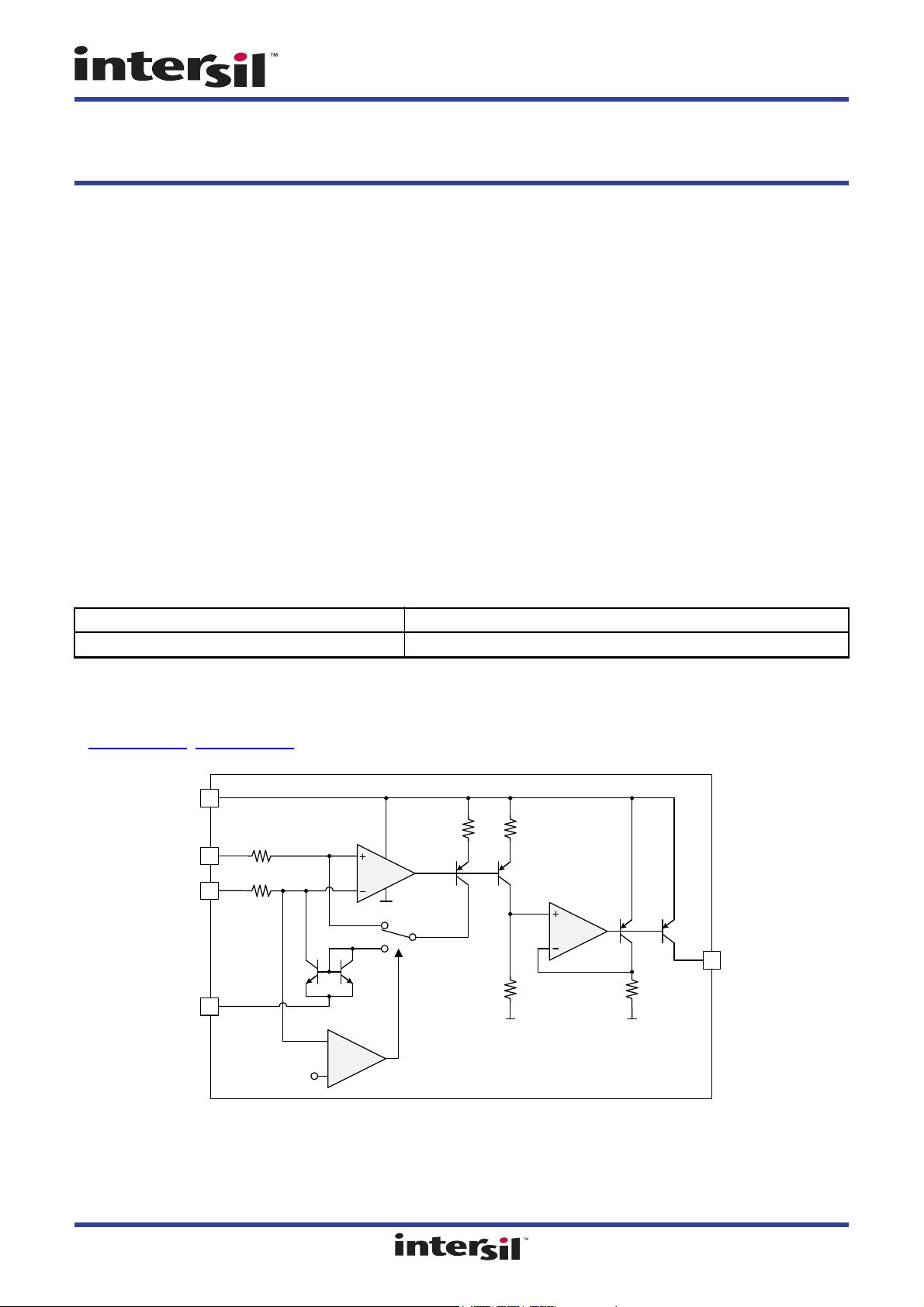
The ISL73100SEHEV1Z evaluation board is designed to evaluate the performance of the ISL70100SEH and
ISL73100SEH. The ISL70100SEH and ISL73100SEH are radiation hardened 40V current-sense amplifiers built
using the Renesas proprietary PR40 SOI process.
Key Features
• Large current-sense resistor footprint (2512)
• Easy gain configuration using a single resistor
• Kelvin sensing for improved measurement accuracy
Specifications
• Power supply voltage range: 2.7V to 40V
• Current-sense input common-mode range: -0.3V to 40V (regardless of power supply voltage)
• Board dimension: 4.25cm x 5.25cm
• Board layers: Two
• Board revision: A
Ordering Information
Part Number Description
ISL73100SEHEV1Z ISL73100SEHEV1Z evaluation board
Related Literature
For a full list of related documents, visit our website:
• ISL73100SEH
, ISL70100SEH device pages
R34UZ0001EU0100 Rev.1.00 Page 2 of 12
May.28.20
Figure 1. ISL73100SEHEV1Z Block Diagram
Page 3
ISL73100SEHEV1Z 1. Functional Description
(EQ. 1)
ROUT
A
CSA
gm
---------------
=
1. Functional Description
The evaluation board includes a 2512 sized SMD pad for populating a current-sense resistor and an output
termination resistor to set the current-sense to output voltage scaling.
1.1 Operating Range
The ISL70100SEH and ISL73100SEH have a wide power supply range from 2.7V up to 40V. The input
common-mode range extends from -0.3V to 40V, making them ideal to use in both high-side and low-side
current-sense applications. The current-sense amplifiers are voltage-to-current converters that monitor current
using an external sense resistor and output a scaled current of the sensed input voltage.
1.2 Quick Start Guide
1. R2 is a 15mΩ 2512 sized to provide 150mV for 10A. The analog differential input voltage for RS+ to RS- is 0V
to 150mV. If R2 needs to be changed, the product of the current-sense resistance and maximum load current
must fall within 150mV.
2. With the load unbiased: Connect the current-sense terminals to the circuit load either in a high-side sense (RS+
goes to load positive supply rail, RS- goes to load positive terminal) or low-side sense (RS+ goes to load
negative terminal, RS- goes to load negative supply rail) configuration.
3. Provide a power supply voltage to V+ (BA1) and GND (BA2) terminals of the ISL73100SEHEV1Z board. The
power supply voltage range is 2.7V to 40V.
4. Power-up load.
5. The voltage on OUT (BNC1) with the 25kΩ output resistor is 50mV for every 1mV input sense voltage. The
full-scale 150mV input produces 7.5V output.
Note: To use the full-scale output voltage at 150mV full-scale input sense voltage with the 25kΩ output resistor,
the minimum supply range must be increased to 9.5V to account for the 2.0V output head-room to the V+
supply voltage.
1.3 Current-Sense Resistor
To pick the current-sense resistor value, a decision has to be made between power dissipation and measurement
accuracy. As a general rule for all applications, the sense resistor should be as small as possible while still
providing adequate input dynamic range across the operating range. The minimum accurately sensed input
voltage is primarily limited by the offset voltage of the ISL70100SEH and ISL73100SEH.
The sense resistor value can be calculated when the maximum load current is determined. The maximum
recommended sense voltage for the amplifier is 150mV, so dividing that by the maximum load current provides
the sense resistor value.
The current-sense error is the amplifier offset voltage divided by the current-sense resistor.
On the ISL73100SEHEV1Z, the current-sense signal is connected to the R2 current-sense resistor in a Kelvin
configuration for sense accuracy.
1.4 Current-Sense Amplifier Output Voltage (Gain Setting)
The ISL73100SEHEV1Z is populated with a 25kΩ resistor at the current-sense amplifier output to GND (BNC
terminal OUT).
The overall gain (A
ISL70100SEH outputs 2µA for every 1mV of differential across the inputs. Equation 1
output load resistance to get a specific gain:
R34UZ0001EU0100 Rev.1.00 Page 3 of 12
May.28.20
) on the ISL70100SEH can be adjusted using a single resistor on the output. The
CSA
can be used to calculate the
Page 4
ISL73100SEHEV1Z 1. Functional Description
For the 25kΩ resistor, the current-sense amplifier gain ACSA is (25mV/µA) * (2µA/mV) = 50V/V. Therefore, at
full-scale of the 150mV input, 300µA output current, the 25kΩ output resistor produces a full-scale output voltage
of 7.5V. Therefore, the output produces 50mV for every 1mV input sense voltage.
1.5 Power Supply Bias Range
The ISL73100SEHEV1Z can be biased anywhere from 2.7V to 40V. The current-sense input common-mode
voltage range is from -0.3V to 40V, regardless of the V+ to V- power supply bias. The current-sense amplifier
output voltage range is V- to 2.0V below V+.
The ISL73100SEHEV1Z is populated with a 25kΩ output resistor that produces 7.5V output voltage at 150mV
full-scale input voltage. To achieve full-scale output voltage, the minimum power supply bias voltage is 9.5V.
If the minimum power supply of 2.7V is used with the 25kΩ output resistor, the maximum accurately sensed
current would be 0.93A.
R34UZ0001EU0100 Rev.1.00 Page 4 of 12
May.28.20
Page 5

ISL73100SEHEV1Z 2. Layout Recommendations
BA2
BA1
R1
25K
BA4
C1
1UF
BNC1
C2
0.1UF
BA3
NC
V-
RS+RS-
V+
NC
LID
OUT
NC
NC
U1
1
2
3
4
5 6
7
8
9
10
R2
.015
OUT
RS+RS-
V+
2. Layout Recommendations
To ensure the best accuracy, Renesas recommends connecting the sense inputs to the sense resistor using a
Kelvin connection. This 4-terminal approach to measurements helps eliminate the losses due to parasitic
resistances in the high current path. To ensure that the bandwidth of the amplifier is not inadvertently
compromised, care must be taken to minimize stray capacitance on the output.
2.1 ISL73100SEHEV1Z Evaluation Board
Figure 2. ISL73100SEHEV1Z (Top)
2.2 ISL73100SEHEV1Z Circuit Schematic
Figure 3. Schematic
R34UZ0001EU0100 Rev.1.00 Page 5 of 12
May.28.20
Page 6

ISL73100SEHEV1Z 3. Bill of Materials
3. Bill of Materials
Reference
Qty
Designator Description Manufacturer Manufacturer Part Number
1 PWB-PCB, ISL73100SEHEV1Z, REVA, ROHS Imagineering Inc ISL73100SEHEV1ZREVAPCB
1 C2 CAP, SMD, 0603, 0.1µF, 100V, 10%, X7R, ROHS Murata GRM188R72A104KA35J
1 C1 CAP, SMD, 1206, 1µF, 100V, 10%, X7R, ROHS Venkel C1206X7R101-105KNE
1 BNC1 CONN-BNC, RECEPTACLE, TH, 4 POST, 50Ω,
SILVERCONTACT, ROHS
4 BA1-BA4 CONN-JACK, MINI BANANA, 0.175 PLUG, NICKEL/BRASS,
ROHS
1 U1 IC-PROTO, RAD HARD, CURRENT SENSE AMP, SMD, 10P,
CDFP
1 R2 RES-AEC-Q200, SMD, 2512, 0.015Ω, 3W, 1%, MF, ROHS Bourns CRA2512-FZ-R015ELF
1 R1 RES, SMD, 0603, 24.9k, 1/10W, 1%, TF, ROHS Panasonic ERJ-3EKF2492V
4 Four corners SCREW, 4-40x1/4in, PHILLIPS, PANHEAD, STAINLESS, ROHS Building Fasteners PMSSS 440 0025 PH
4 Four corners STANDOFF, 4-40x3/4in, F/F, HEX, ALUMINUM, 0.25 OD, ROHS Keystone 2204
Amphenol 31-5329-51RFX
Keystone 575-4
Renesas ISL73100SEHF/PROTO
R34UZ0001EU0100 Rev.1.00 Page 6 of 12
May.28.20
Page 7

ISL73100SEHEV1Z 4. Board Layout
4. Board Layout
Figure 4. Silk Screen Top Figure 5. Top Layer Component Side
Figure 6. Silk Screen Bottom Figure 7. Bottom Layer Solder Side
R34UZ0001EU0100 Rev.1.00 Page 7 of 12
May.28.20
Page 8

ISL73100SEHEV1Z 5. Typical Performance Curves
1.966
1.976
1.986
1.996
2.006
2.016
2.026
-10 0 10 20 30 40
50
Transconductance (µA/mV)
Input Common-Mode Voltage (V)
-55°C
25°C
125°C
-1500
-1000
-500
0
500
1000
1500
-10 0 10 20 30 40
50
Offset Voltage (µV)
Input Common-Mode Voltage (V)
-55°C
25°C
125°C
1.96
1.97
1.98
1.99
2.00
2.01
2.02
-10 0 10 20 30 40 50
Transconductance (µA/mV)
Input Common-Mode Voltage (V)
-55°C
25°C
125°C
I
CC
(A)
-1500
-1000
-500
0
500
1000
1500
-10 0 10 20 30 40 50
Offset Voltage (µV)
Input Common-Mode Voltage (V)
-55°C
25°C
125°C
1.976
1.986
1.996
2.006
2.016
2.026
2.036
-10 0 10 20 30 40 50
Transconductance (µA/mV)
Input Common-Mode Voltage (V)
-55°C
25°C
125°C
-1500
-1000
-500
0
500
1000
1500
-10 0 10 20 30 40 50
Offset Voltage (µV)
Input Common-Mode Voltage (V)
-55°C
25°C
125°C
5. Typical Performance Curves
Recommended operating conditions, V+ = V
= 12V, V- = 0V, V
RS+
SEN
= (V
RS+
- V
RS-
), R
= 5kΩ and TA = +25°C unless otherwise specified.
OUT
Figure 8. Transconductance, V+ = 12V
Figure 9. Common-Mode Voltage vs V
Figure 10. Transconductance, V+ = 40V Figure 11. Common-Mode Voltage vs V
, V+ = 12V
OS
, V+ = 40V
OS
Figure 12. Transconductance, V+ = 2.7V Figure 13. Common-Mode Voltage vs V
R34UZ0001EU0100 Rev.1.00 Page 8 of 12
May.28.20
, V+ = 2.7V
OS
Page 9

ISL73100SEHEV1Z 5. Typical Performance Curves
0
50
100
150
200
250
300
350
-75 -50 -25 0 25 50 75 100 125
150
Supply Current (µA)
Temperature (°C)
VCM = 12V
VCM = 0V
V+ = 12V
0
50
100
150
200
250
300
350
-75 -50 -25 0 25 50 75 100 125
150
Supply Current (µA)
Temperature (°C)
VCM = 2.7V
VCM = 0V
V+ = 2.7V
0
50
100
150
200
250
300
350
-75 -50 -25 0 25 50 75 100 125
150
Supply Current (µA)
Temperature (°C)
VCM = 40V
VCM = 0V
V+ = 40V
I
CC
(A)
0.0
0.2
0.4
0.6
0.8
1.0
1.2
1.4
1.6
1.8
2.0
-75 -50 -25 0 25 50 75 100 125
150
Slew Rate (mA/µs)
Temperature (°C)
2.7V
12V
40V
0
50
100
150
200
250
-75 -50 -25 0 25 50 75 100 125
150
Rise Time 20-80 (ns)
Temperature (°C)
2.7V
12V
40V
0
50
100
150
200
250
300
350
-75 -50 -25 0 25 50 75 100 125
150
Step Reponse Time (ns)
Temperature (°C)
2.7V
12V
40V
Recommended operating conditions, V+ = V
Figure 14. Supply Current, V+ = 12V Figure 15. Supply Current, V+ = 2.7V
= 12V, V- = 0V, V
RS+
SEN
= (V
RS+
- V
RS-
), R
= 5kΩ and TA = +25°C unless otherwise specified.
OUT
Figure 16. Supply Current, V+ = 40V Figure 17. Slew Rate
Figure 18. Rise Time Figure 19. Step Response Time
R34UZ0001EU0100 Rev.1.00 Page 9 of 12
May.28.20
Page 10

ISL73100SEHEV1Z 5. Typical Performance Curves
0.0
0.2
0.4
0.6
0.8
1.0
1.2
-75 -50 -25 0 25 50 75 100 125
150
Settling TIme (µs)
Temperature (°C)
2.7V
12V
40V
0
200
400
600
800
1000
1200
1400
1600
-500
-400
-300
-200
-100
0
100
200
300
0 1020304050
Time (µs)
0.1V/div
0.2mA/div
0.2mA/div
0.2mA/div
VSEN
IOUT (125°C)
IOUT (25°C)
IOUT (-55°C)
-0.5
-0.4
-0.3
-0.2
-0.1
0
0.1
0.2
0.3
0.4
0.5
0
0 20406080100
Time (s)
10V/div
0.1mA/div
0.1mA/div
0.1mA/div
25°C
125°C
-55°C
V+
I
CC
(A)
-1.0
-0.8
-0.6
-0.4
-0.2
0.0
0.2
0.4
0.6
0.8
1.0
0
0 0.2 0.4 0.6 0.8 1
Time (ms)
10V/div
0.2mA/div
0.2mA/div
0.2mA/div
V+
125°C
25°C
-55°C
Recommended operating conditions, V+ = V
Figure 20. Settling Time Figure 21. Input Step Response
= 12V, V- = 0V, V
RS+
SEN
= (V
RS+
- V
RS-
), R
= 5kΩ and TA = +25°C unless otherwise specified.
OUT
Figure 22. Power Supply Ramp at 1V/s Figure 23. Power Supply Ramp at 1V/10µs
R34UZ0001EU0100 Rev.1.00 Page 10 of 12
May.28.20
Page 11

ISL73100SEHEV1Z 6. Revision History
6. Revision History
Rev. Date Description
1.00 May.28.20 Initial release
R34UZ0001EU0100 Rev.1.00 Page 11 of 12
May.28.20
Page 12

IMPORTANT NOTICE AND DISCLAIMER
RENESAS ELECTRONICS CORPORATION AND ITS SUBSIDIARIES (“RENESAS”) PROVIDES TECHNICAL
SPECIFICATIONS AND RELIABILITY DATA (INCLUDING DATASHEETS), DESIGN RESOURCES (INCLUDING
REFERENCE DESIGNS), APPLICATION OR OTHER DESIGN ADVICE, WEB TOOLS, SAFETY INFORMATION, AND
OTHER RESOURCES “AS IS” AND WITH ALL FAULTS, AND DISCLAIMS ALL WARRANTIES, EXPRESS OR IMPLIED,
INCLUDING, WITHOUT LIMITATION, ANY IMPLIED WARRANTIES OF MERCHANTABILITY, FITNESS FOR A
PARTICULAR PURPOSE, OR NON-INFRINGEMENT OF THIRD PARTY INTELLECTUAL PROPERTY RIGHTS.
These resources are intended for developers skilled in the art designing with Renesas products. You are solely responsible
for (1) selecting the appropriate products for your application, (2) designing, validating, and testing your application, and (3)
ensuring your application meets applicable standards, and any other safety, security, or other requirements. These
resources are subject to change without notice. Renesas grants you permission to use these resources only for
development of an application that uses Renesas products. Other reproduction or use of these resources is strictly
prohibited. No lic ense is granted to any other Renesas intellectual property or to any third party intellectual property.
Renesas disclaims responsibility for, and you will fully indemnify Renesas and its representatives against, any claims,
damages, costs, losses, or liabilities arising out of your use of these resources. Renesas' products are provided only subject
to Renesas' Terms and Conditions of Sale or other applicable terms agreed to in writing. No use of any Renesas resources
expands or otherwise alters any applicable warranties or warranty disclaimers for these produc ts.
Corporate Headquarters
TOYOSU FORESIA, 3-2-24 Toyosu,
Koto-ku, Tokyo 135-0061, Japan
www.renesas .com
Trademarks
Renesas and the Renesas logo are trademarks of Renesas
Electronics Corporation. All trademarks and registered
trademarks are the property of their respective owners.
(Rev.1.0 Mar 2020)
Contact Information
For further information on a product, technology, the most
up-to-date version of a document, or your nearest sales
office, please visit:
www.renesas .com/contact/
© 2020 Renesas Electronics Corporation. All rights reserved.
Page 13

ISL73100SEHEV1Z
Renesas Electronics Corporation
www.renesas.com
R34UZ0001EU0100
 Loading...