

Page 1
USER MANUAL
,1
,1
9''
287
*1'
9''
,1
,1%
966
9'59
287+
287/
9663
65&
65&
9
65&
,1
,1
9''
287
*1'
9''
,1
,1%
966
9'59
287+
287/
9663
9
65&
,6/6(+
3:0571
3:0571
9,1
9287
,6/6(+
8
,6/6(+
3:0,1
,6/6(+
,6/0
,6/0
8
8
8
ISL73040SEHEV4Z
Evaluation Board
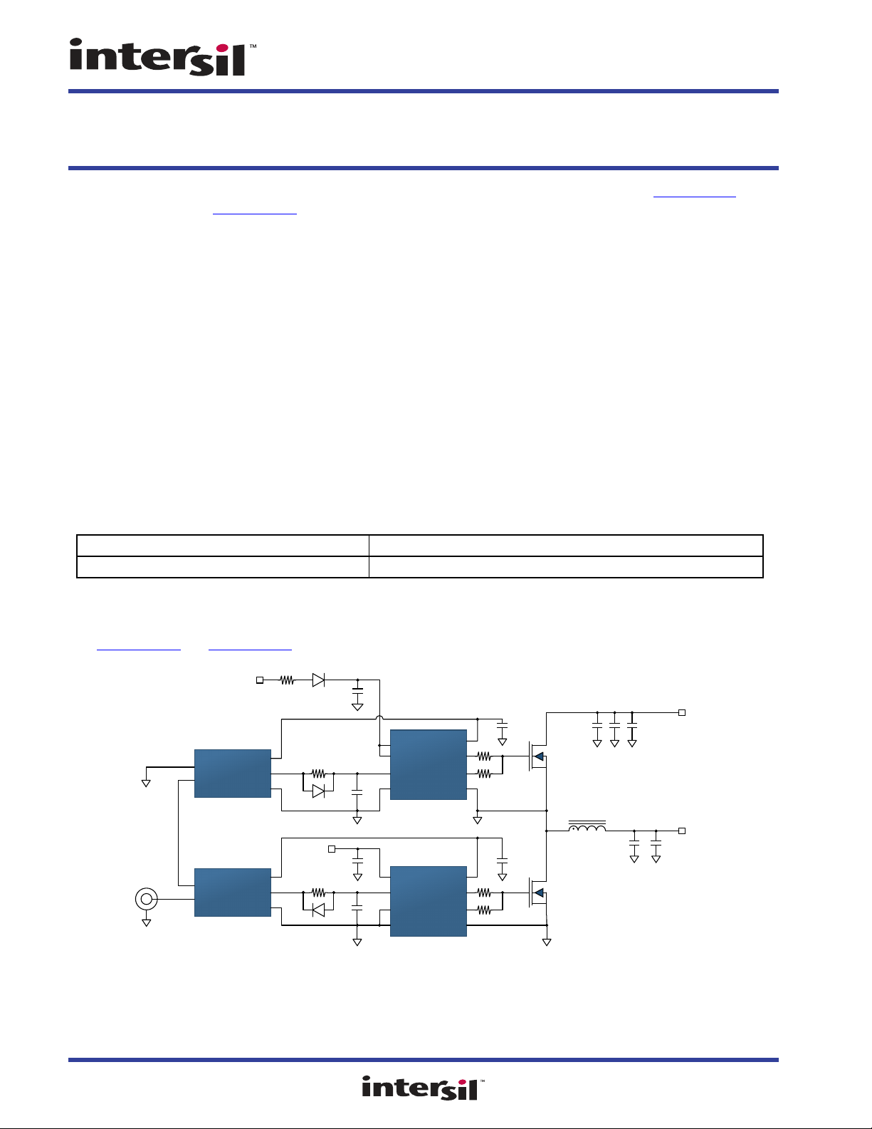
The ISL73040SEHEV4Z evaluation board demonstrates how to build a half bridge power stage with the ISL73040SEH low
side GaN driver and the ISL73024SEH
200V GaN FET. The ISL73040SEH has a 4.5V gate drive voltage (VDRV)
generated using an internal regulator that prevents the gate voltage from exceeding the maximum gate-source rating of the
ISL73024SEH GaN FET. The ISL73024SEH is a 200V GaN FET capable of 7.5A drain current.
Key Features
• Single PWM input to drive a half bridge configuration
• Adjustable dead time control
• Wide openings to support various inductor footprints
• >95% peak efficiency with high switching frequencies
• Enable/disable functions
Specifications
•VDD = 4.5V to 13.2V
•V
= up to 100V (limited by VDS of the GaN FET)
BUS
• PWM input: 40kHz to 1MHz, duty cycle = 2% to 97%
Ordering Information
Mar 24, 2021
UG186
Rev.2.0
Part Number Description
ISL73040SEHEV4Z 100V half bridge power stage evaluation board
Related Literature
For a full list of related documents, visit our website:
• ISL73040SEH
and ISL73024SEH device pages
Figure 1. ISL73040SEHEV4Z Block Diagram
UG186 Rev.2.0 Page 1 of 14
Mar 24, 2021 © 2021 Renesas Electronics
Page 2

ISL73040SEHEV4Z
Contents
1. Functional Description . . . . . . . . . . . . . . . . . . . . . . . . . . . . . . . . . . . . . . . . . . . . . . . . . . . . . . . . . . . . 3
1.1 PWM Input . . . . . . . . . . . . . . . . . . . . . . . . . . . . . . . . . . . . . . . . . . . . . . . . . . . . . . . . . . . . . . . . . . . . 3
1.2 Dead Time Control Adjustment . . . . . . . . . . . . . . . . . . . . . . . . . . . . . . . . . . . . . . . . . . . . . . . . . . . . 3
1.3 Quick Start Guide . . . . . . . . . . . . . . . . . . . . . . . . . . . . . . . . . . . . . . . . . . . . . . . . . . . . . . . . . . . . . . 4
2. Single Events Effects Testing. . . . . . . . . . . . . . . . . . . . . . . . . . . . . . . . . . . . . . . . . . . . . . . . . . . . . . . 5
3. Board Design . . . . . . . . . . . . . . . . . . . . . . . . . . . . . . . . . . . . . . . . . . . . . . . . . . . . . . . . . . . . . . . . . . . . 6
3.1 Schematic Diagrams . . . . . . . . . . . . . . . . . . . . . . . . . . . . . . . . . . . . . . . . . . . . . . . . . . . . . . . . . . . . 7
3.2 Bill of Materials . . . . . . . . . . . . . . . . . . . . . . . . . . . . . . . . . . . . . . . . . . . . . . . . . . . . . . . . . . . . . . . . 8
3.3 Board Layout . . . . . . . . . . . . . . . . . . . . . . . . . . . . . . . . . . . . . . . . . . . . . . . . . . . . . . . . . . . . . . . . . . 9
3.4 PCB Layout Guidelines . . . . . . . . . . . . . . . . . . . . . . . . . . . . . . . . . . . . . . . . . . . . . . . . . . . . . . . . . 12
4. Typical Performance Curves. . . . . . . . . . . . . . . . . . . . . . . . . . . . . . . . . . . . . . . . . . . . . . . . . . . . . . . 13
5. Revision History. . . . . . . . . . . . . . . . . . . . . . . . . . . . . . . . . . . . . . . . . . . . . . . . . . . . . . . . . . . . . . . . . 14
UG186 Rev.2.0 Page 2 of 14
Mar 24, 2021
Page 3
ISL73040SEHEV4Z 1. Functional Description
0
20
40
60
80
100
012345
% of Capacitor Voltage
Time Constant (τ)
0
20
40
60
80
100
012345
% of Capacitor Voltage
Time Constant (τ)
R
6
t
don
1.1668
100
12–
10 F
--------------------------------------=
(EQ. 1)
1. Functional Description
The ISL73040SEHEV4Z demonstrates how to use the ISL73040SEH and ISL73024SEH in a half bridge
configuration. The following sections describe how to tune the evaluation board for a given application.
1.1 PWM Input
The input signal frequency is limited to 40kHz to 1MHz with a duty cycle between 2% and 97%, and is fed into J7.
The input is designed to accommodate voltages between 3.3V and 10V to be compatible with readily available
PWM controllers on the market. The input signal is fed into two ISL71610M front ends in series, which can be
simplified into coils with a coil resistance of 128Ω each. R
of the ISL71610M. Assuming the input voltage is 3.3V, R
ISL71610M front end to 8mA (steady state), and C
times. R
(1MΩ) and C56 (100pF) are optional, but provide the ability to isolate the incoming signal from power
22
provides the instantaneous current for quicker rise and fall
55
ground.
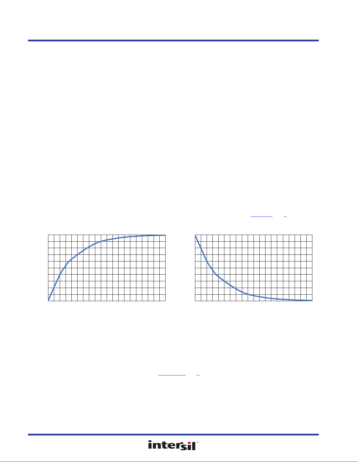
1.2 Dead Time Control Adjustment
The dead time control is adjusted based on the RC charge and discharge times of R6/C54 and R5/C22. The
ISL73040SEH has inverting and non-inverting inputs that provide complimentary drive for the upper and lower
GaN FETs. D
lower resistance path during turn-off.
Dead time is controlled by turning off the active GaN FET quickly and delaying the turn-on of the inactive FET.
Select the R and C values so that the charge and discharge times to the logic thresholds of the ISL73040SEH are
equal to the desired dead time. The ideal RC charge and discharge profiles are shown in Figures 2
respectively:
and D4 ensure that the turn-on time is delayed only for the high-side and low-side by providing a
3
and C55 control the current going into the input coils
20
is set to 150Ω, which limits the current into the
20
and 3,
Figure 2. RC Charge Profile Figure 3. RC Discharge Profile
The final capacitor voltage is 4.5V because the V
of the ISL71610M is tied to the VDRV of its respective gate
DD
driver. As the high side GaN FET is driven with an inverted logic signal, the dead time for turning on the high-side
is determined by how long the RC filter takes to discharge from 4.5V down to the V
is 31.1% of 4.5V (V
up to the V
of the ISL73040SEH, which is 37.8% of 4.5V (VIH =1.7V). These percentages yield time constant
IH
= 1.4V). The dead time for turning on the low-side is gated by the RC filter’s charging time
IL
of the ISL73040SEH, which
IL
multiples of 1.1668τ for the high-side dead time, and 0.4721τ for the low-side dead time (where τ is the time
constant). The dead time can be calculated using Equations 1
and 2 by choosing a capacitor value (100pF is used in
this design) and calculating the needed resistance.
where t
UG186 Rev.2.0 Page 3 of 14
Mar 24, 2021
is the high-side dead time, in seconds.
don
Page 4

ISL73040SEHEV4Z 1. Functional Description
(EQ. 2)
R
5
t
doff
0.4721
100
12–
10 F
---------------------------------------=
where t
For example, a t
R
6
propagation delay mismatches between the high-side and low-side drivers (U
isolators (U
is the low-side dead time, in seconds.
doff
(high side dead time) of 16ns and a t
don
(low side dead time) of 30ns yields R5 = 635Ω and
doff
= 137Ω. Use common resistor values to round R5 = 620Ω and R6 = 140Ω. These calculations do not account for
) and the high-side and low-side
), so the final value on the board may need to be adjusted to achieve the desired results. Figure 15
3/U4
1/U2
on page 13 shows the actual dead times that result from using R5 = 620Ω and R6 = 140Ω.
1.3 Quick Start Guide
The following equipment is needed to evaluate the board:
• Bus power supply: a power supply capable of 100V with 5A current capability
• Bias power supply: a power supply capable of 5V to 12V with 1A current capability
• Function generator capable of producing a square wave up to 1MHz with duty cycle control
• Electronic load capable of 7A
• Digital multimeter to measure V
OUT
1.3.1 Operation Procedure
(1) Connect the bus power supply between VBUS and GND (J3/J4).
(2) Connect the bias power supply between J
(3) Connect the function generator the BNC jack (J
(4) Connect the electronic load to VOUT and GND (J
(5) Connect the digital multimeter between VOUT and GND (J
(6) Set the bias power supply to any voltage between 5V and 12V. In this example it is set to 5V.
(7) Set the bus power supply to 100V.
(8) Set the electronic load anywhere up to 7A. The inductor on the evaluation platform is rated for 10.5A with
a 20°C rise in temperature, so 7A provides enough margin.
(9) Set the function generator to output a square wave with 28% duty cycle at 500kHz.
(10) Set the function generator output voltage levels to V
limited 10V, because of a 25mA coil rating. The input coils of U
(11) Turn on the bias power supply.
(12) Turn on the bus power supply.
(13) Turn on the function generator output.
(14) V
should be roughly 28% of the bus supply voltage (100V in this example).
OUT
(15) Turn on the electronic load.
(16) V
drops below 28V. The duty cycle of the function generator can be modified to return V
OUT
and J2.
1
) on the board.
7
).
5/J6
).
5/J6
= 0.0V and VOH = 3.3V. The PWM voltage is
OL
and U4 are specified at 128Ω (max) each.
3
OUT
to 28V.
UG186 Rev.2.0 Page 4 of 14
Mar 24, 2021
Page 5

ISL73040SEHEV4Z 2. Single Events Effects Testing
2. Single Events Effects Testing
The ISL73040SEHEV4Z, which uses the ISL71610M isolators and the ISL73040SEH drivers was evaluated for
shoot-through under heavy ions. The following is the test setup:
• VDD = 12V
• VBUS = 28V
• L1 was depopulated
•A 1Ω current-sense resistor was placed in line with the drain of Q1
• A 1MHz, 0V-5V signal was provided to J7
•LET = 86MeV•cm
• Fluence = 1x10
The voltage at the drain of Q1 was monitored on an oscilloscope for events with a trigger window of ±50mV around
the nominal voltage at the drain. A shoot-through event under heavy ions turned on Q1 and Q2, pulling the Q1 drain
significantly below VBUS. A 50mV trigger window across 1Ω represents 50mA of shoot-through current. For the
first test, both isolators (ISL71610M) were simultaneously exposed to heavy ions, no events were captured. For the
second test, both drivers (ISL73040SEH) were simultaneously exposed to heavy ions with no events captures. In
conclusion, there were no shoot-through events recorded for the half-bridge configuration used in the
ISL73040SEHEV4Z evaluation board up to an LET of 86 MeV•cm
2
/mg
7
ions/cm
2
2
/mg.
UG186 Rev.2.0 Page 5 of 14
Mar 24, 2021
Page 6

ISL73040SEHEV4Z 3. Board Design
3. Board Design
Figure 4. ISL73040SEHEV4Z Evaluation Board (Top)
UG186 Rev.2.0 Page 6 of 14
Mar 24, 2021
Page 7

Mar 24, 2021
Prop delay = 12-18nsec (typ/max)
600pF for 20mA boost current assuming
3.3V input signal with 100ns rise/fall times
150 ohms for 8mA current assuming
3.3V input signal with 2x 128ohm coils
Input range from 3.3V to 10V
10V limit due to 25mA max dc-current rating of coils
40kHz lower-limit due to 25uSec hold-up time of high-side bootstrap
Prop delay skew = +/- 2nsec (max diff between units at 25C)
Prop delay mismatch = +/- 5 nsec (max diff)
Dead time = 15nsec (low-to-high) compensates for +/- 7nsec uncertainty
27nsec (high-to-low) ZVS @ 100V, >1.7A
Dead-time = 27nsec
Dead-time = 15nsec
Diode is flipped because of inverting logic to driver
Delay "turn-on" timing of both switches to generate dead time
Duty cycle = 2% to 97%
At 2% duty-cycle, high-to-low dead-time drops to 22nsec
<2% duty, >97% duty causes one gate to drop out
Input frequency = 40kHz to 1MHz
Power Connectors
Input is fully isolated from ground
RC for ESD / RF connection
low-side enable/disable
Normally short pins 1-2
0
0
0
Source
SourceSource
Source
0
Source
Source
0
0
Source
0
0
0 0
0
0
0
0
Source
Source
0
Source
0
C48
0.47uF
10%
500V
12
C31
0.47uF
10%
500V
12
C59
0.47uF
10%
500V
12
E14
1
C23
0.1uF
10%
630V
12
C44
0.47uF
10%
500V
12
C53
0.1uF
10%
10V
12
E8
1
J4
1
E4
1
C7
0.1uF
10%
10V
12
E17
1
J5
1
L1
22UH
20%
1 2
D1
JANTX1N5617US
C22
100pF
2%
100V
12
C62
0.47uF
10%
500V
12
C26
0.47uF
10%
500V
12
C3
0.047uF
10%
25V
12
R1
0.0
63MW
1%
1 2
C49
0.47uF
10%
500V
12
D4
JANTX1N6640
C5
2.2uF
10%
16V
12
C29
0.47uF
10%
500V
12
J7
POM_4578
1
2
C45
0.47uF
10%
500V
12
E2
1
E15
1
J6
1
C1
4.7uF
10%
25V
12
E10
1
J8
Header_Pin
1
1
2
2
3
3
C54
100pF
2%
100V
12
D3
JANTX1N6640
C8
0.047uF
10%
25V
12
R3
0.0
63MW
1%
1 2
R2111250mW
1%
12
E6
1
C56
100pF
2%
100V
12
C60
0.47uF
10%
500V
12
E5
1
U1
ISL7040SEH
VDD
1
IN
2
INB
3
VSS4VSSP
5
OUTL
6
OUTH
7
VDRV
8
C24
0.1uF
10%
630V
12
E18
1
S
G
D
Q1
ISL7024SEH
4
1 3
2
E1
1
C50
0.47uF
10%
500V
12
R2
0.0
63MW
1%
1 2
R5
620
63MW
1%
1 2
E11
1
C46
0.47uF
10%
500V
12
C55
560pF
100V
2%
12
E16
1
C2
2.2uF
10%
25V
12
C27
0.47uF
10%
500V
12
C42
0.47uF
10%
500V
12
C9
2.2uF
10%
25V
12
C30
0.47uF
10%
500V
12
R4
0.0
63MW
1%
1 2
C4
0.1uF
10%
10V
12
S
G
D
Q2
ISL7024SEH
4
1 3
2
J1
1
E12
1
R6
140
63MW
1%
1 2
C11
0.1uF
10%
630V
12
U4
I6/0
IN+
2
IN-
3
GND
5
OUT
6
V_OE
7
VDD
8
C51
0.47uF
10%
500V
12
C47
0.47uF
10%
500V
12
R22
1000k
250mW
1%
1
2
C61
0.47uF
10%
500V
12
E7
1
R20
150
250mW
1%
12
C43
0.47uF
10%
500V
12
J2
1
C10
4.7uF
10%
25V
12
C25
0.1uF
10%
630V
12
E9
1
E3
1
C58
2.2uF
10%
16V
12
C6
2.2uF
10%
16V
12
U3
I6/0
IN+
2
IN-
3
GND
5
OUT
6
V_OE
7
VDD
8
U2
ISL7040SEH
0
Prop delay mismatch = +/- 5 nsec (max diff)
VDD
1
IN
2
INB
3
VSS4VSSP
5
OUTL
6
OUTH
7
VDRV
8
C57
2.2uF
10%
16V
12
C28
0.47uF
10%
500V
12
C21
0.1uF
10%
10V
12
J3
1
E13
1
Source
HS 5-12V
LS 5-12V
HS 4.5V
LS 4.5V
HS 4.5V
Vout
LS 5-12V
LS 4.5V
PWM_RTN
PWM
LS 5-12V Vbus Vout
PWM_RTN
LS 4.5V
Vbus
UG186 Rev.2.0 Page 7 of 14
ISL73040SEHEV4Z 3. Board Design
3.1 Schematic Diagrams
Figure 5. ISL73040SEHEV4Z Board Schematic
Page 8

Mar 24, 2021
UG186 Rev.2.0 Page 8 of 14
ISL73040SEHEV4Z 3. Board Design
3.2 Bill of Materials
Qty Reference Designator Description EDM Manufacturer
2 C1, C10 4.7µF Capacitor, X7R, 25V, 1812 KEMET C1812F475K5RAC7800 AVX G311P838-A-FX475K1R1
6 C2, C5, C6, C9, C57, C58 2.2µF Capacitor, X7R, 25V, 1206 KEMET C1206C225K3RACTU AVX G311P838-A-DX225K1R1
2 C3, C8 0.047µF Capacitor, X7R, 25V, 0402 KEMET C0402C473K3RACAUTO Presidio G311P829-A-AX473K1N1
4 C4, C7, C21, C53 0.1µF Capacitor, X7R, 10V, 0402 KEMET C0402C104K4RALTU Presidio G311P829-A-AX104K1N1
4 C11, C23, C24, C25 0.1µF Capacitor, X7R, 250V, 1210 KEMET C1210C104KBRACAUTO KEMET C1210T104KARAL
3 C22, C54, C56 100pF Capacitor, NP0, 100V, 0805 AVX 08051A101GAT2A Presidio SR0805NP0101G3NT9
20 C26, C27, C28, C29, C30,
C31, C42, C43, C44, C45,
C46, C47, C48, C49, C50,
C51, C59, C60, C61, C62
1 C55 560pF Capacitor, NP0, 100V, 0805 AVX 08051A561GAT2A Presidio SR0805NP0561G3NT9
1 D1 Diode 400V 1A, D5A Microsemi 1N5617US Microsemi JANS1N5617US
2 D3, D4 Diode 50V 300mA, D5D Microsemi 1N6640US Microsemi JANS1N6640
18 E1, E2, E3, E4, E5, E6, E7,
E8, E9, E10, E11, E12, E13,
E14, E15, E16, E17, E18
6 J1, J2, J3, J4, J5, J6 Banana Jack Keystone Electronics 575-8 N/A N/A
1 J7 BNC Jack Pomona 4578 N/A N/A
1 J8 Header Pin Samtec TSW-103-07-F-S N/A N/A
1 L1 Inductor 22µH
2 Q1, Q2 GaN FET 200V 45mΩ 7.5A Renesas ISL73024SEHL/PROTO Renesas ISL73024SEH
4 R1, R2, R3, R4 Resistor 0Ω Jumper, 0402 Vishay Beyschlag MCS04020Z0000ZE000 Vishay M32159B11T
1 R5 Resistor 619Ω 1%, 0805 Vishay Dale CRCW0805619RFKEA Vishay M55342K06B619DS
1 R6 Resistor 140Ω 1%, 0805 Vishay Dale CRCW0805140RFKEA Vishay M55342K06B140DS
1 R20 Resistor 150Ω 1%, 1206 Vishay Dale CRCW1206150RFKEA Vishay D55342K07B150DS
1 R21 Resistor 11Ω 1%, 1206 Vishay Dale CRCW120611R0FKEA Vishay D55342K07B11D0S
1 R22 Resistor 1000kΩ 1%, 1206 Vishay Dale CRCW12061M00FKEA Vishay D55342K07B1F00S
2 U1, U2 RH Low-Side GaN FET Driver Renesas ISL73040SEHL/PROTO Renesas ISL73040SEH
2 U3, U4 RT Digital Isolator Renesas ISL71610M Renesas ISL71610M
0.47µF Capacitor, X7R, 250V, 1812 KEMET 1812PC474KAT2A KEMET C1812T474KARAL
Test point E20AWG N/A N/A N/A N/A
Coilcraft XAL1510-223 Coilcraft AE612PNB223MSZ
Note: Flight Inductor DCR >> EDM DCR
EDM Manufacturer
Part Number
Flight
Manufacturer
Flight Manufacturer
Part Number
Page 9

ISL73040SEHEV4Z 3. Board Design
3.3 Board Layout
Figure 6. Silkscreen Top
Figure 7. Layer 1 (Component Side)
UG186 Rev.2.0 Page 9 of 14
Mar 24, 2021
Page 10

ISL73040SEHEV4Z 3. Board Design
Figure 8. Layer 2
Figure 9. Layer 3
UG186 Rev.2.0 Page 10 of 14
Mar 24, 2021
Page 11

ISL73040SEHEV4Z 3. Board Design
Figure 10. Layer 4
UG186 Rev.2.0 Page 11 of 14
Mar 24, 2021
Page 12

ISL73040SEHEV4Z 3. Board Design
3.4 PCB Layout Guidelines
When replicating this layout in a system, pay attention to the following guidelines:
• Place the driver as close as possible to the driven power FET
• Understand where the switching power currents flow. The high amplitude di/dt currents of the driven power FET
induce significant voltage transients on the associated traces
• Keep power loops as short as possible by paralleling the source and return traces
• Use planes where practical; they are usually more effective than parallel traces
• Avoid paralleling high amplitude di/dt traces with low level signal lines. High di/dt induces currents and
consequently, noise voltages in the low level signal lines
• When practical, minimize impedances in low level signal circuits. The noise that is magnetically induced on a
10kΩ resistor is 10 times larger than the noise on a 1kΩ resistor
• Be aware of magnetic fields emanating from transformers and inductors. Gaps in the magnetic cores of these
structures emit lots of flux
• If you must place traces close to magnetic devices, align the traces to be parallel to the flux lines to minimize
coupling
• Use decoupling capacitors to reduce the influence of parasitic inductance in the V
be effective, these capacitors must also have the shortest possible conduction paths. If using vias, connect several
paralleled vias to reduce the inductance of the vias
• It may be necessary to add resistance to dampen resonating parasitic circuits, especially on OUTH. If an external
gate resistor is unacceptable, the layout must be improved to minimize lead inductance
• Keep high dv/dt nodes away from low level circuits. Guard banding can be used to shunt away dv/dt injected
currents from sensitive circuits. This is especially true for control circuits that source the input signals to the
ISL73040SEH
• Avoid placing signal ground planes under high amplitude dv/dt circuits. This injects di/dt currents into the signal
ground paths
• Calculate power dissipation and voltage drop for the power traces. Many PCB/CAD programs have built-in tools
for calculating trace resistance
• Large power components (such as power FETs, electrolytic caps, and power resistors) have internal parasitic
inductance which cannot be eliminated. Account for this in the PCB layout and circuit design
• If the circuits are simulated, consider including parasitic components, especially parasitic inductance
• The GaN FETs have a separate substrate connection that is internally tied to the source pin. Source and substrate
should be at the same potential. Limit the inductance in the OUTH/L to Gate trace by keeping it as short and thick
as possible
, VDD, and GND leads. To
DRV
UG186 Rev.2.0 Page 12 of 14
Mar 24, 2021
Page 13

ISL73040SEHEV4Z 4. Typical Performance Curves
82%
84%
86%
88%
90%
92%
94%
96%
98%
0 10203040506070
Efficiency (%)
Power Out (W)
82%
84%
86%
88%
90%
92%
94%
96%
98%
020406080100
Efficiency (%)
Power Out (W)
82%
84%
86%
88%
90%
92%
94%
96%
98%
0 10203040506070
Efficiency (%)
Power Out (W)
82%
84%
86%
88%
90%
92%
94%
96%
98%
020406080100
Efficiency (%)
Power Out (W)
-2
-1
0
1
2
3
4
5
6
0 0.2 0.4 0.6 0.8
1
Voltage (V)
Time (µs)
HS Gate
LS Gate
19.8 ns
27.5 ns
-2
-1
0
1
2
3
4
5
6
0 0.2 0.4 0.6 0.8
1
Voltage (V)
Time (µs)
HS Gate
LS Gate
t
FALL
3.2ns
t
RISE
6.7ns
t
RISE
6.1ns
t
FALL
3.2ns
4. Typical Performance Curves
Unless noted: fSW = 500kHz, TA = +25°C
Figure 11. V
Figure 13. V
= 28V, V
BUS
= 100V, V
BUS
= 12V
OUT
= 28V Figure 14. V
OUT
Figure 12. V
BUS
= 120V, V
BUS
= 70V, V
OUT
OUT
= 28V
= 100V
Figure 15. Dead Time Between HS and LS Gate Figure 16. Rise and Fall Times
UG186 Rev.2.0 Page 13 of 14
Mar 24, 2021
Page 14

ISL73040SEHEV4Z 5. Revision History
5. Revision History
Rev. Date Description
2.0 Mar 24, 2021 Removed Front and Back Covers
Added TOC.
Added the SEE Testing section.
1.0 Feb 26, 2019 Updated Figures 2, 3, and 16.
0.0 Nov 20, 2018 Initial release
UG186 Rev.2.0 Page 14 of 14
Mar 24, 2021
Page 15

IMPORTANT NOTICE AND DISCLAIMER
RENESAS ELECTRONICS CORPORATION AND ITS SUBSIDIARIES (“RENESAS”) PROVIDES TECHNICAL
SPECIFICATIONS AND RELIABILITY DATA (INCLUDING DATASHEETS), DESIGN RESOURCES (INCLUDING
REFERENCE DESIGNS), APPLICATION OR OTHER DESIGN ADVICE, WEB TOOLS, SAFETY INFORMATION, AND
OTHER RESOURCES “AS IS” AND WITH ALL FAULTS, AND DISCLAIMS ALL WARRANTIES, EXPRESS OR IMPLIED,
INCLUDING, WITHOUT LIMITATION, ANY IMPLIED WARRANTIES OF MERCHANTABILITY, FITNESS FOR A
PARTICULAR PURPOSE, OR NON-INFRINGEMENT OF THIRD PARTY INTELLECTUAL PROPERTY RIGHTS.
These resources are intended for developers skilled in the art designing with Renesas products. You are solely responsible
for (1) selecting the appropriate products for your application, (2) designing, validating, and testing your application, and (3)
ensuring your application meets applicable standards, and any other safety, security, or other requirements. These
resources are subject to change without notice. Renesas grants you permission to use these resources only for
development of an application that uses Renesas products. Other reproduction or use of these resources is strictly
prohibited. No lic ense is granted to any other Renesas intellectual property or to any third party intellectual property.
Renesas disclaims responsibility for, and you will fully indemnify Renesas and its representatives against, any claims,
damages, costs, losses, or liabilities arising out of your use of these resources. Renesas' products are provided only subject
to Renesas' Terms and Conditions of Sale or other applicable terms agreed to in writing. No use of any Renesas resources
expands or otherwise alters any applicable warranties or warranty disclaimers for these produc ts.
Corporate Headquarters
TOYOSU FORESIA, 3-2-24 Toyosu,
Koto-ku, Tokyo 135-0061, Japan
www.renesas .com
Trademarks
Renesas and the Renesas logo are trademarks of Renesas
Electronics Corporation. All trademarks and registered
trademarks are the property of their respective owners.
(Rev.1.0 Mar 2020)
Contact Information
For further information on a product, technology, the most
up-to-date version of a document, or your nearest sales
office, please visit:
www.renesas .com/contact/
 Loading...