

Page 1
User’s Manual
ISL71043MEVAL1Z
Evaluation Board
The ISL71043MEVAL1Z evaluation platform is designed to evaluate the ISL71043M and ISL71040M in a flyback
power supply configuration.
The ISL71043M is a radiation tolerant drop-in replacement for the popular 28C4x and 18C4x PWM controllers
suitable for a wide range of power conversion applications including boost, flyback, and isolated output
configurations. This evaluation board is a flyback power supply. The board features up to 13.2V V
low operating current, 90μA typical start-up current, adjustable operating frequency to 1MHz, and high peak
current drive capability with 50ns rise and fall times.
The ISL71040M is a low-side driver designed to drive enhancement mode Gallium Nitride (GaN) FETs in isolated
topologies and boost type configurations. The ISL71040M operates with a supply voltage from 4.5V to 13.2V and
has inverting (INB) and non-inverting (IN) inputs to satisfy requirements for both inverting and non-inverting gate
drives with a single device. The ISL71040M has a 4.5V gate drive voltage (V
internal regulator, which prevents the gate voltage from exceeding the maximum gate-source rating of
enhancement mode GaN FETs. The gate drive voltage also features an Undervoltage Lockout (UVLO) protection
that ignores the inputs (IN and INB) and keeps OUTL turned on, ensuring that the GaN FET is in an OFF state
when V
the V
outputs of the ISL71040M offer the flexibility to independently adjust the turn-on and turn-off speeds by adding
additional impedance to the turn-on and turn-off paths.
is below the UVLO threshold. The ISL71040M inputs can withstand voltages up to 14.7V regardless of
DRV
voltage, which allows the ISL71040M inputs to be connected directly to most PWM controllers. The split
DD
) that is generated using an
DRV
operation,
DD
Key Features
• 24W flyback power supply
• Option to power the ISL71043M and ISL71040M using the auxiliary winding on a flyback transformer or
separate power supply
•V
• Tight line/load regulation: 0.003%/0.16%
within 1% of 12V with 0A to 2A load step
OUT
Specifications
•Wide VIN range single: 22V to 36V
•Wide V
•I
OUT
range single: 7.5V to 13.2V
DD
range: 0A to 2A
Ordering Information
Part Number Description
ISL71043MEVAL1Z Flyback Power Supply
Related Literature
For a full list of related documents, visit our website:
• ISL71043M and ISL71040M device pages
R12UZ0044EU0200 Rev.2.0 Page 1 of 14
Feb.9.21 Copyright © 2019
Page 2

ISL71043MEVAL1Z 1. Functional Description
1. Functional Description
The ISL71043MEVAL1Z is a flyback power supply that takes an input voltage between 22V and 36V and outputs
12V with a max load capability of 2A.
1.1 Operating Range
The ISL71043M offers a wide operating supply range of 8V to 13.2V. The ISL71040M accepts a VDD range of
4.5V to 13.2V. The gate drive voltage for the ISL70023SEH is generated by the ISL71040M from an internal linear
regulator to keep the gate-to-source voltage below the absolute maximum VGS level of 6V.
1.2 Quick Start Guide
1. Choose how VDD for the ISL71043M and ISL71040M is provided:
a. Short Pins 1-2 on JP
b. Short Pins 2-3 on JP
2. Apply 28V to the VIN input (BA
to provide 12V VDD from an external power supply using BA3 and BA4.
1
to power the ICs from the auxiliary winding from the transformer.
1
and BA2).
1
3. Power up VIN and VDD.
4. The 12V regulated output is on BA
5. Monitor the VGS voltage using TP
6. Monitor the VDS voltage using TP
and BA6.
5
and TP3 with a short-to-ground loop connection on a scope probe.
2
and TP3 with a short-to-ground loop connection on a scope probe.
13
7. Use SP2 to monitor the current on the primary side.
1.3 Undervoltage Lockout (UVLO)
The ISL71043M UVLO follows a fairly standard implementation where the it does not allow any operation until a
valid VDD is cleared. The rising UVLO edge on the ISL71043M is 9V (maximum), while the falling edge is assured
to trigger by 8V (minimum).
The ISL71040M UVLO monitors the gate drive voltage as opposed to V
level, the output is held low and the inputs are ignored, which is done due to GaN’s low turn-on threshold
(compared to MOSFETs). When VDRV < ~1V, an internal 500Ω resistor connected between OUTL and ground
helps keep the gate voltage close to ground. When ~1.2V < VDRV < UV, OUTL is actively driven low while
ignoring the logic inputs, and OUTH is in a high impedance state. The low state has the same current sinking
capacity as during normal operation ensuring that the driven FETs are held off. The FETs are held off even if there
is a switching voltage on the drains that can inject charge into the gates from the Miller capacitance.
. Until VDRV passes an acceptable
DD
When VDRV > UVLO, the ISL71040M waits for the next rising edge on INB or falling edge on IN before the output
starts to follow the inputs. This additional check can prevent runt pulses from being generated because the first
pulse is always a controlled pulse from the PWM regulator. When the UCVLO is cleared, the outputs now respond
to the logic inputs. In the non-inverting operation (PWM signal applied to IN pin), the output is in-phase with the
input. In the inverting operation (PWM signal applied to INB pin), the output is out-phase with the input.
For the negative transition of VDRV through the UV lockout voltage, when VDRV < ~3.7V
the OUTL is active
DC
low and OUTH is high impedance regardless of the input logic states.
1.4 VDD Power Supply
The ISL71043MEVAL1Z provides the ability to choose how to power the VDD of the ISL71043M and ISL71040M.
Using JP
use an external power supply.
R12UZ0044EU0200 Rev.2.0 Page 2 of 14
Feb.9.21
, you can choose to short Pins 2-3 to use the auxiliary winding of the transformer or short Pins 1-2 to
1
Page 3

ISL71043MEVAL1Z 2. General PCB Layout Guidelines
2. General PCB Layout Guidelines
The AC performance of the ISL71040M depends significantly on the design of the Printed Circuit Board (PCB).
The following layout design guidelines are recommended to achieve optimum performance:
• Place the driver as close as possible to the driven power FET.
• Understand where the switching power currents flow. The high amplitude di/dt currents of the driven power FET
induce significant voltage transients on the associated traces.
• Keep power loops as short as possible by paralleling the source and return traces.
• Use planes where practical; they are usually more effective than parallel traces.
• Avoid paralleling high amplitude di/dt traces with low level signal lines. High di/dt induces currents and
consequently, noise voltages in the low level signal lines.
• When practical, minimize impedances in low level signal circuits. The noise, magnetically induced on a 10kΩ
resistor, is 10 times larger than the noise on a 1kΩ resistor.
• Be aware of magnetic fields emanating from transformers and inductors. Gaps in the magnetic cores of these
structures are especially bad for emitting flux.
• If you must have traces close to magnetic devices, align the traces so that they are parallel to the flux lines to
minimize coupling.
• The use of low inductance components such as chip resistors and chip capacitors is highly recommended
• Use decoupling capacitors to reduce the influence of parasitic inductance in the VDRV, VDD, and GND leads.
To be effective, these capacitors must also have the shortest possible conduction paths. If vias are used,
connect several paralleled vias to reduce the inductance of the vias.
• It may be necessary to add resistance to dampen resonating parasitic circuits, especially on OUTH. If an
external gate resistor is unacceptable, then the layout must be improved to minimize lead inductance.
• Keep high dv/dt nodes away from low level circuits. Guard banding can be used to shunt away dv/dt injected
currents from sensitive circuits, which is especially true for control circuits that source the input signals to the
ISL71040M.
• Avoid having a signal ground plane under a high amplitude dv/dt circuit, which injects di/dt currents into the
signal ground paths.
• Calculate power dissipation and voltage drop for the power traces. Many PCB/CAD programs have built in tools
for trace resistance calculation.
• Large power components (such as power FETs, electrolytic caps, and power resistors) have internal parasitic
inductance that cannot be eliminated., which must be accounted for in the PCB layout and circuit design.
• If you simulate your circuits, consider including parasitic components, especially parasitic inductance.
• The GaN FETs have a separate substrate connection that is internally tied to the source pin. Source and
substrate should be at the same potential. Limit the inductance in the OUTH/L to Gate trace by keeping it as
short and thick as possible.
R12UZ0044EU0200 Rev.2.0 Page 3 of 14
Feb.9.21
Page 4
R12UZ0044EU0200 Rev.2.0 Page 4 of 14
29
272523
21191715131197531
30282624
22
201816
1412108642
ISL73023SEH
Source
Drain
Double U p On Several Layers as per Current Needs
Double Up On Several Layers as per Current Needs
ISL71040M
VDRV
VDD
OUTH
OUTL
VSSP
IN
INB
VSS
Feb.9.21
ISL71043MEVAL1Z 2. General PCB Layout Guidelines
Figure 1. PCB Layout Recommendation
Page 5
ISL71043MEVAL1Z 2. General PCB Layout Guidelines
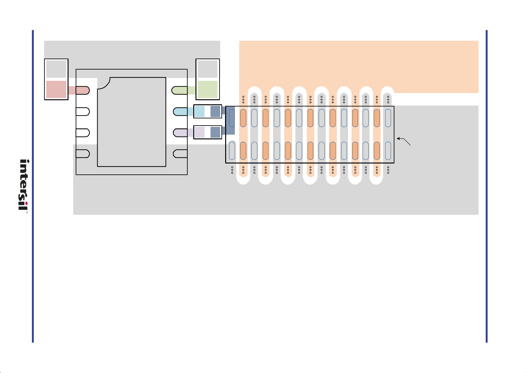
2.1 ISL71043MEVAL1Z Evaluation Board
Figure 2. ISL71043MEVAL1Z Evaluation Board, Top View
Figure 3. ISL71043MEVAL1Z Evaluation Board, Bottom View
R12UZ0044EU0200 Rev.2.0 Page 5 of 14
Feb.9.21
Page 6

Feb.9.21
RELEASED BY:
DRAWN
BY:
DATE:
DATE:
DATE:
TESTER
DATE:ENGINEER:
TITLE:
UPDATED BY:
02/28/2019
ISL71043M
KIRAN BERNARD
TIM KLEMANN
SCHEMATIC
EVALUATION BOARD
GND
+22V-36V
VDD
SOURCE
*
*
PGND
PGND
GND
DRAIN
PGND
*
GND
+12V/2A
VOUT'
GND
GATE
PLACE CLOSE TO U2
A
A
A
A
A
A
A
A
A
A
A
A
A
A
A
A
A
A
E
E
A
E
E
OUT
OUT
1UF
C9C
TP12
C16C
0.1UF
C7C
820PF
C4
100V
0.01UF
R27
0
BA4
NC
NC
105883AK-1
T1
1
2
3
4 5
6
7
8
BA6
R24
1K
R1
1W
3.01K
R6
30.1K
R22
10K
VSSP
INB
VSS
EPAD
IN
VDD
OUTL
OUTH
VDRV
U2
ISL71040MRTZ
1
2
3
4 5
6
7
8
9
21K
R10
TP9
0
R2
D8
BAT54C-7-F
1
2
3
C13C
1200PF
TP2
120UF
C1
D5
12
C10C
0.22UF
SP2
1
234
COMP
FB
CS
RTCTGND
OUT
VDD
VREF
ISL71043MBZ
U1
1
2
3
45
6
7
8
C15C
6800PF
BA3
C17
DNP
12
R18
10
3.6
R7
D9
BZT52C10T
12
1N4148WS-7-F
D7
12
180UF
C5
1200PF
C18C
1UF
C3C
D1
B340LB
12
22UF
C2A
BCX55-16
Q2
R4
20
SUB
S14
S13
S12
S11
S10
S9S8S7S6S5S3S4S2S1
D3D4D5
GATE
D9D8D7
D6
D2
D1
D14
D13
D12
D10
D11
Q1
ISL70023SEHX/SAMPLE
22UF
C2B
D4
12
4.7UF
C2C
0.1UF
C19C
R5
10K
R26
10K
549
R8
R11
17.8K
BA2
390PF
C12C
TP11
C8C
220PF
TP3
TP1
C20C
4.7UF
TP10
C6A
22UF
7.5
R23
TP7
BA1
0
R3
D3
PDS560-13
1
2
3
TP13
2.1K
R9
120UF
C21
TP4
SP1
1
234
TP6
Q3
MMBT2222
1
2
3
C14C
2700PF
D2
BAS70T-7-F
21
0
R25
SECPRI
PA1005.100NL
T2
13
7 8
BA5
JP1
1 2 3
TP8
0.22UF
C11C
TP5
COMP
CS
FB
OUT
RTCT
SEC
UNNAMED_1_0805CAP_I1150_B
UNNAMED_1_105883AK_I1345_AUX1N
UNNAMED_1_105883AK_I1345_PRIM1N
UNNAMED_1_1N4148_I1287_CAT
UNNAMED_1_BCX55_I1381_B
UNNAMED_1_BCX55_I1381_E
UNNAMED_1_ISL70023SEH_I1374_D1
UNNAMED_1_ISL70023SEH_I1374_GATE
UNNAMED_1_ISL71040M_I1375_PIN6
UNNAMED_1_ISL71040M_I1375_PIN7
UNNAMED_1_ISL71040M_I1375_PIN8
UNNAMED_1_JUMPER3_I1286_IN3
UNNAMED_1_MMBT2222_I1146_E
UNNAMED_1_PA1005_I1329_1
UNNAMED_1_SMCAP_I1202_B
UNNAMED_1_SMCAP_I1350_B
UNNAMED_1_SMCAP_I1364_A
UNNAMED_1_SMCAP_I1364_B
UNNAMED_1_SMCAP_I1366_B
UNNAMED_1_SMRES_I1187_B
UNNAMED_1_SMRES_I1278_A
UNNAMED_1_SMRES_I1278_B
VDD
VDD_IN
VIN
VOUT
VREF
R12UZ0044EU0200 Rev.2.0 Page 6 of 14
2.2 ISL71043MEVAL1Z Schematic Diagram
ISL71043MEVAL1Z 2. General PCB Layout Guidelines
Figure 4. ISL71043MEVAL1Z Schematic
Page 7

ISL71043MEVAL1Z 2. General PCB Layout Guidelines
2.3 Bill of Materials
Qty
1 PWB-PCB, ISL71043MEVAL1Z, REVB, ROHS Imagineering Inc ISL71043MEVAL1ZREVBPCB
1 C2 CAP-AEC-Q200, SMD, 0805, 4.7µF, 25V, 10%, X7R,
2 C16, C19 CAP, SMD, 0603, 0.1µF, 50V, 10%, X7R, ROHS AVX 06035C104KAT2A
2 C13, C18 CAP, SMD, 0603, 1200pF, 50V, 10%, X7R, ROHS Panasonic ECJ-1VB1H122K
1 C8 CAP, SMD, 0603, 220pF, 50V, 5%, C0G, ROHS Venkel C0603COG500-221JNE
1 C14 CAP, SMD, 0603, 2700pF, 50V, 10%, X7R, ROHS Panasonic ECJ-1VB1H272K
1 C12 CAP, SMD, 0603, 390pF, 50V, 5%, NP0, ROHS Panasonic ECJ-1VC1H391J
1 C20 CAP, SMD, 0603, 4.7µF, 10V, 10%, X5R, ROHS Venkel C0603X5R100-475KNE
1 C15 CAP, SMD, 0603, 6800PF, 50V, 10%, X7R, ROHS AVX 06035C682KAT9A
1 C7 CAP, SMD, 0603, 820pF, 50V, 10%, X7R, ROHS Kemet C0603C821K5RACTU
1 C4 CAP, SMD, 0805, 0.01µF, 100V, 10%, X7R, ROHS Panasonic ECJ-2VB2A103K
1 C9 CAP, SMD, 0805, 1.0µF, 25V, 10%, X5R, ROHS AVX 08053C105KAT2A
Reference
Designator Description Manufacturer Manufacturer Part
TDK CGA4J1X7R1E475K125AC
ROHS
2 C10, C11 CAP, SMD, 0805, 0.22µF, 25V, 10%, X7R, ROHS Panasonic Default
1 C3 CAP, SMD, 1206, 1µF, 50V, 10%, X7R, ROHS Venkel C1206X7R500-105KNE
3 C6, C2A, C2B CAP, SMD, 1210, 22µF, 16V, 10%, X7R, ROHS Murata GRM32ER71C226KE18L
1 C5 CAP-OSCON, SMD, 8.3mm, 180µF, 16V, 20%, ROHS Sanyo 16SVP180M
2 C1, C21 CAP-AEC-Q200, SMD, 10.3mm, 120µF, 50V, 20%,
28mOhm, ROHS
1 C17 CAP-X1, Y2, SMD, 2211, 1500pF, 250V, 10%, X7R,
ROHS
2 SP1, SP2 CONN-SCOPE PROBE TEST PT, COMPACT, PCB
MNT, ROHS
2 BA3, BA4 CONN-TURRET, TERMINAL POST, TH, ROHS Keystone 1514-2
12 TP2-TP13 CONN-MINI TEST POINT, VERTICAL, WHITE, ROHS Keystone 5002
1 TP1 CONN-MINI TEST POINT, SMD, 0.105x0.040, ROHS Keystone 5015
4 BA1, BA2, BA5, BA6 CONN-JACK, MINI BANANA, 0.175 PLUG,
NICKEL/BRASS, ROHS
1 JP1 CONN-HEADER, 1x3, BREAKAWY 1x36, 2.54mm,
ROHS
1 D7 DIODE-RECTIFIER, SMD, SOD-323, 2P, 75V, 150mA,
ROHS
1 D1 DIODE-SCHOTTKY, SMD, SMB, 2P, 40V, 3A LOW VF,
ROHS
Panasonic EEH-ZC1H121P
Murata GA352QR7GF152KW01L
Tektronix 131-4353-00
Keystone 575-4
Berg/FCI 68000-236HLF
Diodes Inc. 1N4148WS-7-F
Diodes Inc. B340LB-13-F
R12UZ0044EU0200 Rev.2.0 Page 7 of 14
Feb.9.21
Page 8

ISL71043MEVAL1Z 2. General PCB Layout Guidelines
Reference
Qty
1 D2 DIODE-SCHOTTKY, SMD, SOT-523, 70V, 70mA,
Designator Description Manufacturer Manufacturer Part
ROHS
Micro Commercial
Co.
BAS70T-TP
1 D8 DIODE-RECTIFIER, SMD, SOT23, 30V, 200mA,
2 D4, D9 DIODE-ZENER, SMD, SOD-523, 10V, 150mW, ROHS Diodes, Inc. BZT52C10T-7
1 D5 DIODE-ZENER, SMD, SOD-123, 15V, 500mW, ROHS Diodes, Inc. BZT52C15-7-F
1 D3 DIODE-RECTIFIER, SMD, POWER DI5, 3P, 60V, 5A,
1 U1 IC-CURRENT MODE PWM, 8P, SOIC, 8.4V, ROHS Renesas
1 Q1 IC-DIE SAMPLE, RAD HARD 100V GAN FET Renesas
1 Q2 TRANSISTOR, NPN, SMD, SOT-89, 4P, 60V, 1A,
1 Q3 TRANSISTOR, NPN, 3LD, SOT23, 40V, 600mA,
2 R2, R3 RES, SMD, 0402, 0Ω, 1/16W, 5%, TF, ROHS Venkel CR0402-16W-00T
1 R25 RES, SMD, 0603, 0Ω, 1/10W, TF, ROHS Venkel CR0603-10W-000T
1 R24 RES, SMD, 0603, 1k, 1/10W, 1%, TF, ROHS Panasonic ERJ-3EKF1001V
3 R5, R22, R26 RES, SMD, 0603, 10k, 1/10W, 1%, TF, ROHS Venkel CR0603-10W-1002FT
DUAL DIODE, ROHS
Diodes Inc. PDS560-13
ROHS
ISL71043MBZ
Electronics
America
ISL73023SEHX/SAMPLE
Electronics
Diodes, Inc. BCX55-16
ROHS
ROHS
1 R11 RES, SMD, 0603, 17.8k, 1/10W, 1%, TF, ROHS Panasonic ERJ-3EKF1782V
1 R9 RES, SMD, 0603, 2.1k, 1/10W, 1%, TF, ROHS Yageo 9C06031A2101FKHFT
1 R10 RES, SMD, 0603, 21k, 1/10W, 1%, TF, ROHS Venkel CR0603-10W-2102FT
1 R8 RES, SMD, 0603, 549Ω, 1/10W, 1%, TF, ROHS Venkel CR0603-10W-5490FT
1 R18 RES, SMD, 0805, 10Ω, 1/8W, 1%, TF, ROHS Venkel CR0805-8W-10R0FT
1 R4 RES, SMD, 0805, 20Ω, 1/8W, 1%, TF, ROHS KOA RK73H2AT20R0F
1 R27 RES, SMD, 0805, 0Ω, 1/8W, TF, ROHS Yageo RC0805JR-070RL
1 R23 RES, SMD, 2512, 7.5Ω, 1W, 1%, TF, ROHS Panasonic ERJ-1TRQF7R5U
1 R6 RES-AEC-Q200, SMD, 0603, 30.1k, 1/10W, 0.1%,
ThinFilm, ROHS
1 R1 RES-AEC-Q200, SMD, 2512, 3.01k, 1W, 1%, TF,
100ppm, ROHS
1 R7 RES-AEC-Q200, SMD, 2512, 3.6Ω, 1W, 1%, TF,
400ppm, ROHS
1 T2 TRANSFORMERURR.SENSE, SMD, 8x7, 6P, 20A,
1:1RATIO, ROHS
4 Four corners SCREW, 4-40x1/4in, PHILLIPS, PANHEAD,
STAINLESS, ROHS
Susumu RG1608P-3012-B-T5
KOA RK73H3ATTE3011F
Stackpole RMCF2512FT3R60
Pulse PA1005.100NL
Building Fasteners PMSSS 440 0025 PH
R12UZ0044EU0200 Rev.2.0 Page 8 of 14
Feb.9.21
Page 9

ISL71043MEVAL1Z 2. General PCB Layout Guidelines
Reference
Qty
4 Four corners STANDOFF, 4-40x3/4in, F/F, HEX, ALUMINUM, 0.25
Designator Description Manufacturer Manufacturer Part
Keystone 2204
OD, ROHS
1 T1 TRANSFORMER-FLYBACK, 3.3µH, 5%, 500KHz,
SMD, 8P, 0.8x0.650in, ROHS
1 U2 IC-GaN FET Driver, MIL TEMPL.8LD, 4x4, TDFN,
RoHS
2.4 Board Layout
Vanguard
Electronics
Renesas ISL71040MRTZ
105883AK-1
Figure 5. Top Silkscreen
Figure 6. Bottom Silkscreen
R12UZ0044EU0200 Rev.2.0 Page 9 of 14
Feb.9.21
Page 10

ISL71043MEVAL1Z 2. General PCB Layout Guidelines
Figure 7. Top Layer
Figure 8. Second Layer
R12UZ0044EU0200 Rev.2.0 Page 10 of 14
Feb.9.21
Page 11

ISL71043MEVAL1Z 2. General PCB Layout Guidelines
Figure 9. Third Layer
Figure 10. Bottom Layer
R12UZ0044EU0200 Rev.2.0 Page 11 of 14
Feb.9.21
Page 12

ISL71043MEVAL1Z 3. Typical Performance Curves
12.050
12.060
12.070
12.080
12.090
12.100
12.110
12.120
12.130
12.140
12.150
0.0 0.5 1.0 1.5
2.0
V
OUT
(V)
I
OUT
(A)
VIN= 28V
Load Reg: 0.16%
12.092
12.093
12.094
12.095
12.096
12.097
12.098
20 25 30 35
40
V
OUT
(V)
VIN(V)
Line Reg.: 0.003%
I
OUT
= 1.0A
11.2
11.4
11.6
11.8
12.0
12.2
12.4
12.6
12.8
051015
20
V
OUT
(V)
Time (µs)
V
P-P
: 80.0mV
+0.42%/-0.25% of V
OUT
-2.0
-1.6
-1.2
-0.8
-0.4
0.0
0.4
0.8
1.2
1.6
2.0
11.7
11.8
11.9
12.0
12.1
12.2
12.3
12.4
12.5
12.6
12.7
0.0 0.5 1.0 1.5 2.0
I
OUT
(A)
V
OUT
(V)
Time (ms)
VOUT
IOUT
0
10
20
30
40
50
60
70
80
90
100
0.0 0.5 1.0 1.5
2.0
Efficiency (%)
I
OUT
(A)
-250
-200
-150
-100
-50
0
50
100
150
200
250
-100
-80
-60
-40
-20
0
20
40
60
80
100
10 100 1k 10k 100k 1M
Phase (°)
Gain (dB)
Frequency (Hz)
Gain
Phase
Gain Margin: -39.14 dB
Phase Margin: 60.70°
fCO: 4,685 kHz
3. Typical Performance Curves
Figure 11. Load Regulation Figure 12. Line Regulation
Figure 13. Output Ripple
Figure 15. Efficiency
R12UZ0044EU0200 Rev.2.0 Page 12 of 14
Feb.9.21
Figure 14. Step Transient
Figure 16. Stability VIN = 28V, V
OUT
= 12V, I
OUT
=1A
Page 13

ISL71043MEVAL1Z 3. Typical Performance Curves
-250
-200
-150
-100
-50
0
50
100
150
200
250
-100
-80
-60
-40
-20
0
20
40
60
80
100
10 100 1k 10k 100k 1M
Phase (°)
Gain (dB)
Frequency (Hz)
Gain
Phase
Gain Margin: -27.69 dB
Phase Margin: 65.97°
fCO: 4,816 kHz
1 10 100
1
10
100
10
3
RT (kΩ)
Frequency (kHz)
100pF
220pF
330pF
470pF
1.0nF
2.2nF
3.3nF
4.7nF
6.8nF
Figure 17. Stability VIN = 28V, V
OUT
= 12V, I
= 2A Figure 18. RTCT Frequency
OUT
R12UZ0044EU0200 Rev.2.0 Page 13 of 14
Feb.9.21
Page 14
ISL71043MEVAL1Z 4. Revision History
4. Revision History
Rev. Date Description
2.0 Feb.9.21 Updated BOM, board photos, layout, and schematic.
1.0 Mar.28.19 Initial release
R12UZ0044EU0200 Rev.2.0 Page 14 of 14
Feb.9.21
Page 15

IMPORTANT NOTICE AND DISCLAIMER
RENESAS ELECTRONICS CORPORATION AND ITS SUBSIDIARIES (“RENESAS”) PROVIDES TECHNICAL
SPECIFICATIONS AND RELIABILITY DATA (INCLUDING DATASHEETS), DESIGN RESOURCES (INCLUDING
REFERENCE DESIGNS), APPLICATION OR OTHER DESIGN ADVICE, WEB TOOLS, SAFETY INFORMATION, AND
OTHER RESOURCES “AS IS” AND WITH ALL FAULTS, AND DISCLAIMS ALL WARRANTIES, EXPRESS OR IMPLIED,
INCLUDING, WITHOUT LIMITATION, ANY IMPLIED WARRANTIES OF MERCHANTABILITY, FITNESS FOR A
PARTICULAR PURPOSE, OR NON-INFRINGEMENT OF THIRD PARTY INTELLECTUAL PROPERTY RIGHTS.
These resources are intended for developers skilled in the art designing with Renesas products. You are solely responsible
for (1) selecting the appropriate products for your application, (2) designing, validating, and testing your application, and (3)
ensuring your application meets applicable standards, and any other safety, security, or other requirements. These
resources are subject to change without notice. Renesas grants you permission to use these resources only for
development of an application that uses Renesas products. Other reproduction or use of these resources is strictly
prohibited. No license is granted to any other Renesas intellectual property or to any third party intellectual property.
Renesas disclaims responsibility for, and you will fully indemnify Renes as and its representatives against, any claims,
damages, costs, losses, or liabilities arising out of your use of these resources. Renesas' products are provided only subject
to Renesas' Terms and Conditions of Sale or other applicable terms agreed to in writing. No use of any Renesas resources
expands or otherwise alters any applicable warranties or warranty disclaimers for these products.
Corporate Headquarters
TOYOSU FORESIA, 3-2-24 Toyosu,
Koto-ku, Tokyo 135-0061, Japan
www.renesas .com
Trademarks
Renesas and the Renesas logo are trademarks of Renesas
Electronics Corporation. All trademarks and registered
trademarks are the property of their respective owners.
(Rev.1.0 Mar 2020)
Contact Information
For further information on a product, technology, the most
up-to-date version of a document, or your nearest sales
office, please visit:
www.renesas .com/contact/
 Loading...