

Page 1

User’s Manual
ISL70005SEHEV2Z
High Reliability
User’s Manual: Evaluation Board
All information contained in these materials, including products and product specifications,
represents information on the product at the time of publication and is subject to change by
Renesas Electronics Corp. without notice. Please review the latest information published by
Renesas Electronics Corp. through various means, including the Renesas Electronics Corp.
website (http://www.renesas.com).
Renesas Electronics Corporation
www.renesas.com
Rev.1.01
Jan.6.20
Page 2
User’s Manual
ISL70005SEHEV2Z
Evaluation Board
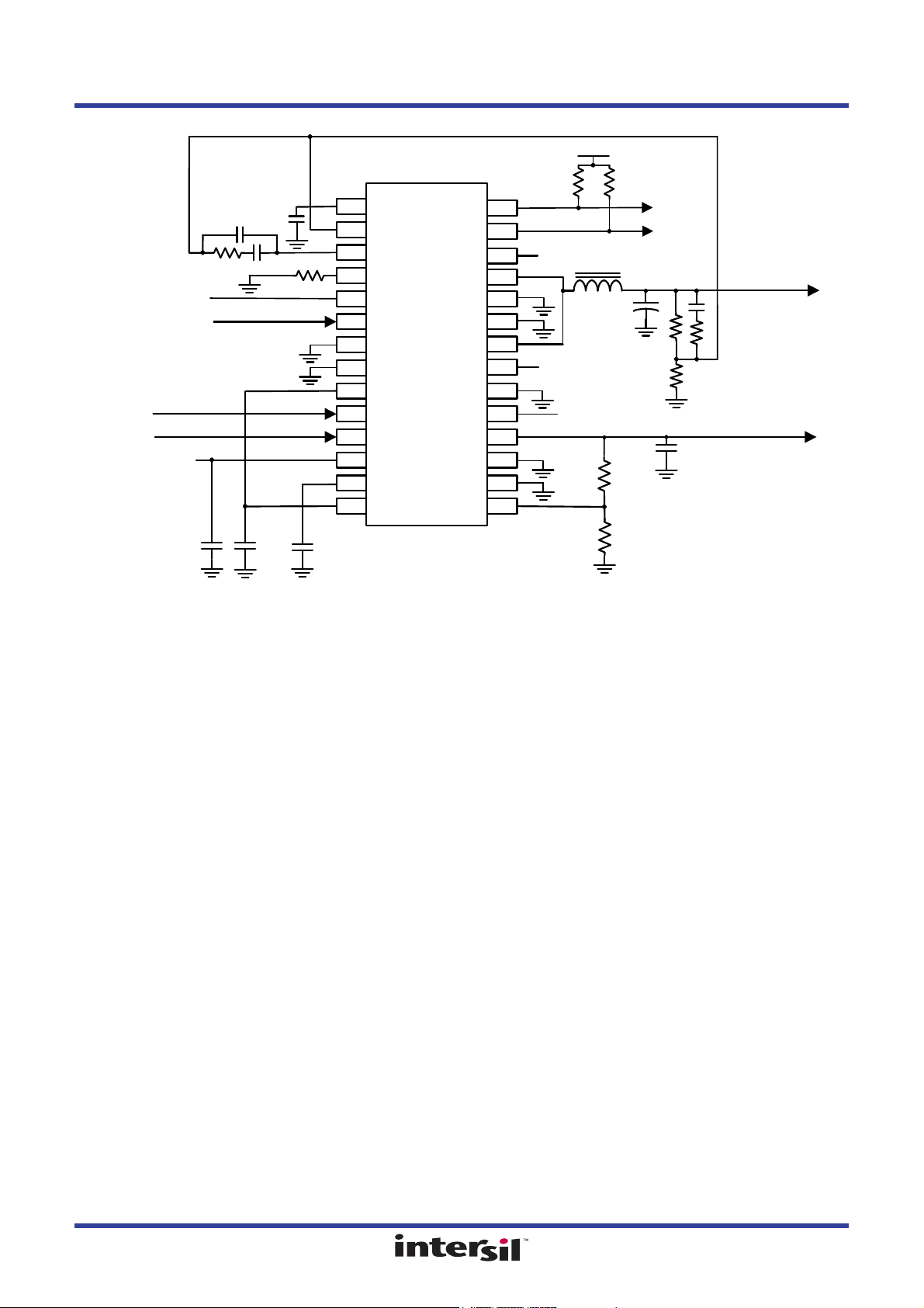
The ISL70005SEHEV2Z evaluation board is designed to evaluate the performance of the ISL70005SEH 3A buck
regulator and 1A source/sink LDO. The evaluation board is optimized for 3V to 5.5V input operation to generate a
3A, 1.8V to 3.3V buck output and a 1A source/sink, 1.2V LDO output. Input and output connections, toggle
switches, and jumper settings on the board provide the customer an easy-to-use evaluation platform for dual rail
supplies for point-of-load, FPGA, and DDR memory power.
Key Features
• Dual point-of-load regulator: 3A buck and 1A source/sink LDO
• Fully independent enable, soft-start, and power-good indicator
• 3V to 5.5V operating voltage
• On-board transient load current generators
Specifications
• Analog and buck regulator input voltage range (PVIN): 3V to 5.5V
• Maximum buck output current: 3A
• Buck preset switching frequency: 1MHz
• LDO input voltage (L_VIN) range: 1.0V to PVIN
• Maximum LDO output (L_OUT) current: 1A sourcing or 1A sinking
• Board dimension: 13.75cm width x 8cm height
• Board layers: Four
• Board PCB copper weight: 2oz.
• Board revision: B
Ordering Information
Part Number Description
ISL70005SEHEV2Z ISL70005SEH evaluation board
Related Literature
For a full list of related documents, visit our website:
• ISL70005SEH
device page
R12UZ0064EU0101 Rev.1.01 Page 2 of 23
Jan.6.20
Page 3
ISL70005SEHEV2Z
B_OUT = 1.8V
26
21
25
22
24
1
2
3
4
5
B_S S
B_FB
B_CO MP
B_RT
B_V CC
B_VIN 2
B_LX2
B_LX1
B_PGND2
B_PGND1
23
28
27
6
7
8
B_SYNC
B_GND1
B_GND2
B_PG
L_PG
TEST
209VREF
B_VIN 1
19
18
10
11
B_E N
L_EN
L_VIN
L_O UT
L_P GND
1712 L_VCC
1613 L_SS L_G ND
L_E A-
1514 L_EA+
+
L_O UT = 1.2V
PVIN = 3V to 5.5V
LVIN = 1V to PVIN
PVIN
ISL70005SEH
Toggle Switch
Toggle Switch
PVIN = 3V to 5.5V
PVIN = 3V to 5.5V
PVIN = 3V to 5.5V
R12UZ0064EU0101 Rev.1.01 Page 3 of 23
Jan.6.20
Figure 1. ISL70005SEHEV2Z Block Diagram
Page 4
ISL70005SEHEV2Z 1. Functional Description
1. Functional Description
1.1 Operating Range
The ISL70005SEHEV2Z has two input supply rails. One for the analog supply and buck power stage input (PVIN)
and the other for the LDO input (L_VIN). The PVIN accepts an input voltage range of 3V to 5.5V while the L_VIN
accepts an input voltage of 1.0V up to PVIN.
The buck regulator output (B_OUT) is capable of sourcing up to 3A. The buck output voltage is board jumper
selectable at 1.8V, 2.5V, 3.3V, or 4.0V. The buck regulator is preset with 1MHz switching frequency with a 2.2µH
output inductor and 150µF output capacitor with the option of being synchronized to an external clock. The LDO
regulator output (L_OUT) is capable of sourcing or sinking up to 1A. The LDO reference input (L_EA+) to the error
amplifier is board jumper selectable to either the 0.6V VREF pin voltage on the ISL70005SEH or ½ the buck
output voltage for DDR VTT rail applications. The LDO output voltage is board jumper selectable to 1.2V or set to
equal the L_EA+ reference voltage.
On-board transient load generators are available for both the buck and LDO for evaluation purposes.
1.2 Quick Start Guides
1.2.1 Dual Independent Buck and LDO Output
1. See Table 1 to set up the jumpers properly to adjust the buck output voltage and configure the LDO for
independent output.
2. Ensure jumper on JP1, JP4, and JP10 are removed. Populate jumper JP6 in the 1-2 position.
3. Apply voltage (3V to 5.5V) to PVIN banana connectors BA1 and BA2.
4. Apply voltage (1.5V to PVIN) to L_VIN banana connectors BA5 and BA7.
5. If the buck enable switch SW1 is on (up position), the buck is enabled and switching at 1MHz. A voltage defined
by the jumper settings of JP2 and JP3 is present on B_OUT at BA3. If SW1 is off (down position), the buck is
disabled and B_OUT = 0V.
6. If the LDO enable switch SW2 is on (up position), the LDO is enabled and a voltage of 1.2V is present on
L_OUT at BA6. If SW2 is off (down position), the LDO is disabled and L_OUT = 0V.
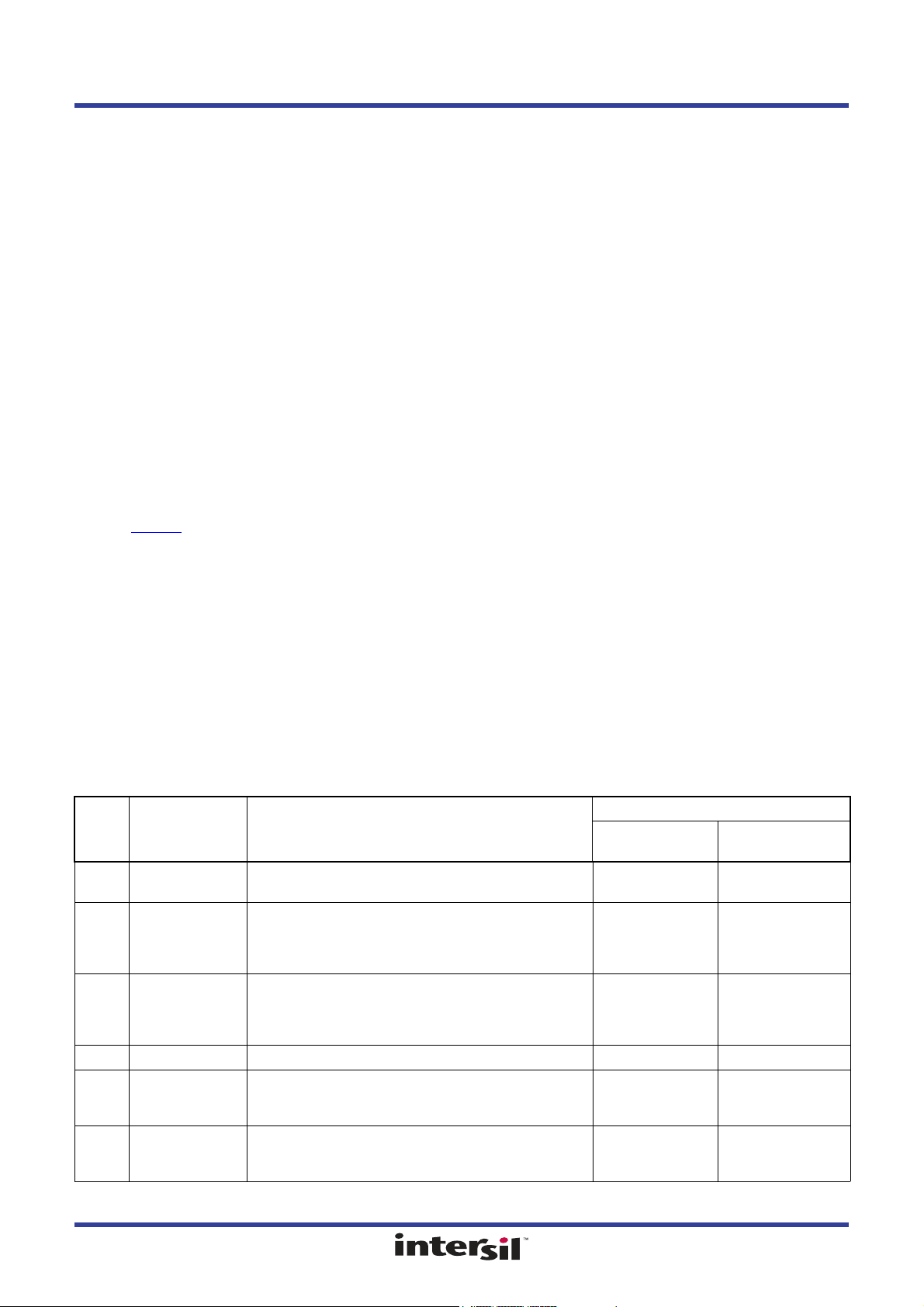
Table 1. Jumper Settings for ISL70005SEHEV2Z
Application Configuration
Independent Buck
Jumper Function Description
JP1 Connects B_EN
and L_EN Together
JP2 Connects R8 to
B_FB
JP3 Connects R7 to
B_FB
JP4 Shorts resistor R21 Populate for LDO unity gain, setting L_OUT = L_EA+. Remove jumper Populate jumper
JP5 External signal
input to SW3
JP6 Connects L_EA+ to
VREF or buck
output
Populate for single switch control of L_EN and B_EN. Remove jumper Populate jumper
Populate for buck output voltage 3.3V. Ensure JP3 is
removed. If no jumper present on JP2 and JP3, buck output
voltage is 1.8V. If JP2 and JP3 both have a jumper, buck
output voltage is programmed to 4V.
Populate for buck output voltage 2.5V. Ensure JP2 is
removed. If no jumper present on JP2 and JP3, buck output
voltage is 1.8V. If JP2 and JP3 both have a jumper, buck
output voltage is programmed to 4V.
Do not populate with jumper. This is a 2-pin header for
connecting an external signal to drive the HI input of HIP2100
when SW3 is in the 2-3 position.
Populate in the 1-2 position for connecting L_EA+ to VREF
pin. Populate in the 2-3 position for connecting to buck output
voltage divided down by the ratio of R15 and R14.
and LDO Regulator
Jumper in 1-2
position
Buck and LDO for
DDR Power
Jumper in 2-3 position
R12UZ0064EU0101 Rev.1.01 Page 4 of 23
Jan.6.20
Page 5
ISL70005SEHEV2Z 1. Functional Description
Table 1. Jumper Settings for ISL70005SEHEV2Z (Continued)
Application Configuration
Jumper Function Description
JP9 Connects L_OUT
to transient load
generator
JP10 Connects buck
V
to resistor
OUT
divider
J1 Connects R18 to
BNC1
J2 Connects R19 to
BNC1
J3 L_OUT voltage
sensing
J4 Buck B_LXx
voltage sensing
J5 PVIN voltage
sensing
J6 L_VIN voltage
sensing
J7 B_OUT voltage
sensing
Populate for connecting to on board LDO transient load
generator.
Populate for connecting buck V
resistor divider network.
Populate for enabling the sinking transient load current
generator on LDO.
Populate for enabling the sourcing transient load current
generator on LDO.
Do not populate with jumper. This is a 2-pin header for
sensing LDO output voltage.
Do not populate with jumper. This is a 2-pin header for
sensing buck regulator switching node.
Do not populate with jumper. This is a 2-pin header for
sensing PVIN voltage.
Do not populate with jumper. This is a 2-pin header for
sensing LDO input voltage.
Do not populate with jumper. This is a 2-pin header for
sensing buck output voltage.
OUT
to the R14 and R15
Independent Buck
and LDO Regulator
Remove jumper Populate jumper
Buck and LDO for
DDR Power
1.2.2 Buck with LDO in DDR Tracking Mode
1. See Table 1 to set up the jumpers properly to adjust the buck output voltage and configure the LDO for tracking
buck output.
2. Ensure jumper on JP1, JP4, and JP10 are populated. Ensure either SW1 or SW2 is off (down position).
Populate jumper JP6 in the 2-3 position.
3. Place a banana cable from BA3 to BA5 to connect B_OUT to L_VIN.
4. Apply voltage (3V to 5.5V) to PVIN banana connectors BA1 and BA2.
5. Because JP1 is populated, connecting B_EN and L_EN together, either SW1 or SW2 toggle switch enables (up
position) and disables (down position) both the buck and LDO together.
6. The LDO L_OUT (VTT rail) is one-half of the buck output voltage (VDDQ rail) determined by the jumper settings
on JP2 and JP3.
7. IMPORTANT: With the buck output powering the LDO input, care must be taken on the output current loading
of the buck regulator. When the LDO is sourcing current, it is supplied by the buck regulator and the buck output
B_OUT 3A limit to external loading is decreased by the LDO load. For example, if LDO is sourcing 1A, the buck
can only provide an additional 2A to the external load.
1.3 Changing Output Voltage on Buck
Jumpers JP2 and JP3 are made available to easily configure the buck output voltage quickly. With no jumpers on
JP2 and JP3, the output voltage is 1.8V. With JP3 only populated, it is 2.5V. With JP2 only populated, it is 3.3V. If
JP2 and JP3 are both populated, it is 4V. If a different output voltage is needed, you must change the R7, R8, or
R43 values. Renesas recommends not changing R10 to preserve the characteristics of the Type III compensation
network.
R12UZ0064EU0101 Rev.1.01 Page 5 of 23
Jan.6.20
Page 6
ISL70005SEHEV2Z 1. Functional Description
100
150
200
250
300
350
400
450
200
300
400
500
600
700
800
100
1000
50
500
Switching Frequency (MHz)
RT Resistor (kΩ)
Table 2. Buck V
V
(V) JP2 Jumper JP3 Jumper
OUT
1.8 Off Off
2.5 Off On
3.3 On Off
4V On On
Jumper Settings
OUT
Note: The buck regulator has minimum on and off times on the B_LXx pins, combined with the switching
frequency, can hit duty cycle limitations for producing the desired output voltage.
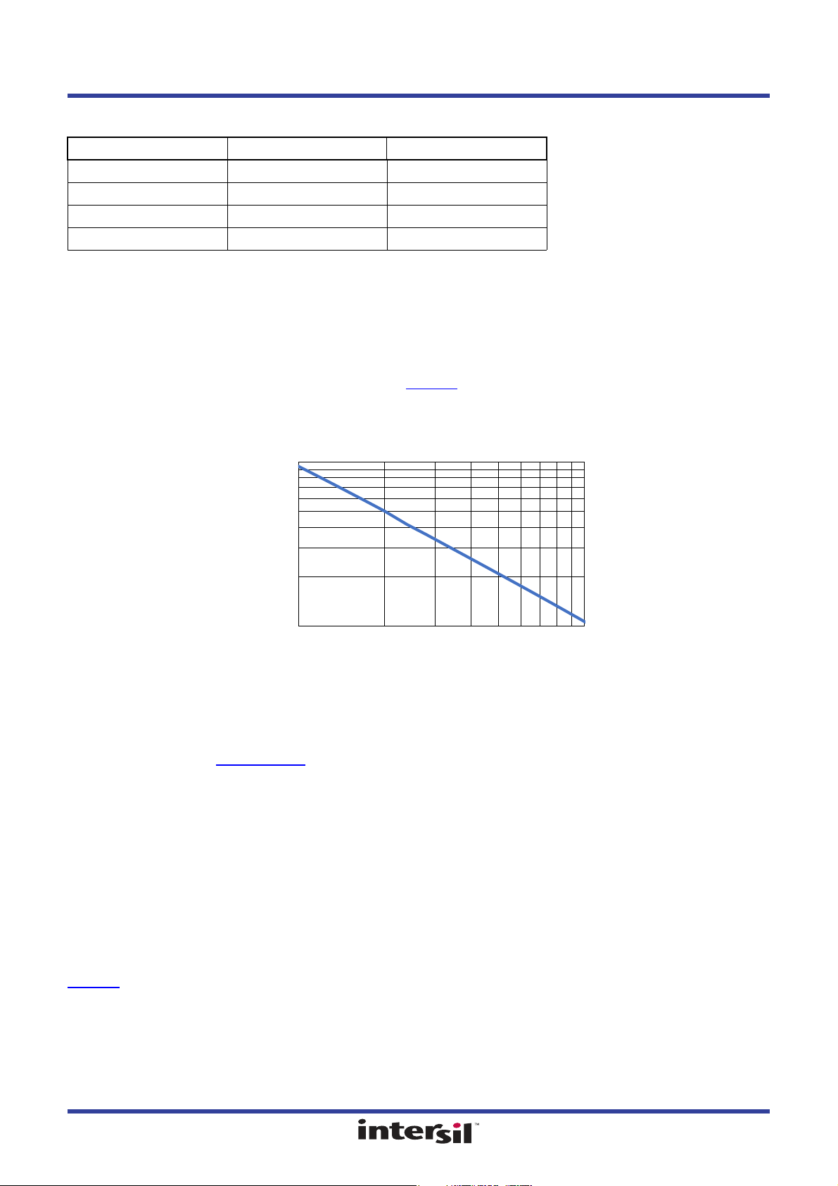
1.4 Changing Buck Switching Frequency
The ISL70005SEHEV2Z is configured for 1MHz switching by using a R4 = 45.3kΩ resistor on B_RT pin to
B_GND. The evaluation board includes a 2.2µH inductor and 150µF tantalum capacitor for the LC output filter. If
you need to select a different switching frequency, see Figure 2
set the switching frequency. The ISL70005SEHEV2Z includes a dual footprint for the inductor to allow for a higher
inductance value with similar saturation current characteristics for the lower switching frequencies.
for selecting the appropriate R4 value on B_RT to
Figure 2. Buck fSW vs RT Resistor on B_RT Pin
1.5 Using External Clock for Buck Switching Frequency
If you need to synchronize the buck switching frequency to an external clock, a test point TP1 is made available
for connection. See the ISL70005SEH
datasheet for more information about external synchronization.
1.6 Changing Buck Output Inductor
The ISL70005SEHEV2Z is populated with a 2.2µH inductor on the L1A footprint targeted for 1MHz switching
frequency. The inductor used on the ISL70005SEHEV2Z is a Coilcraft XFL4020-222ME. If you need to use a
lower switching frequency, a larger inductance must be used to maintain a similar ripple current. The L1B footprint
(inductor not populated) is physically larger to accommodate a larger inductance value with similar saturation
current ratings. For example, with f
= 100kHz the L1B footprint is sized to accommodate a Coilcraft XAL6060-
SW
153ME 15µH inductor.
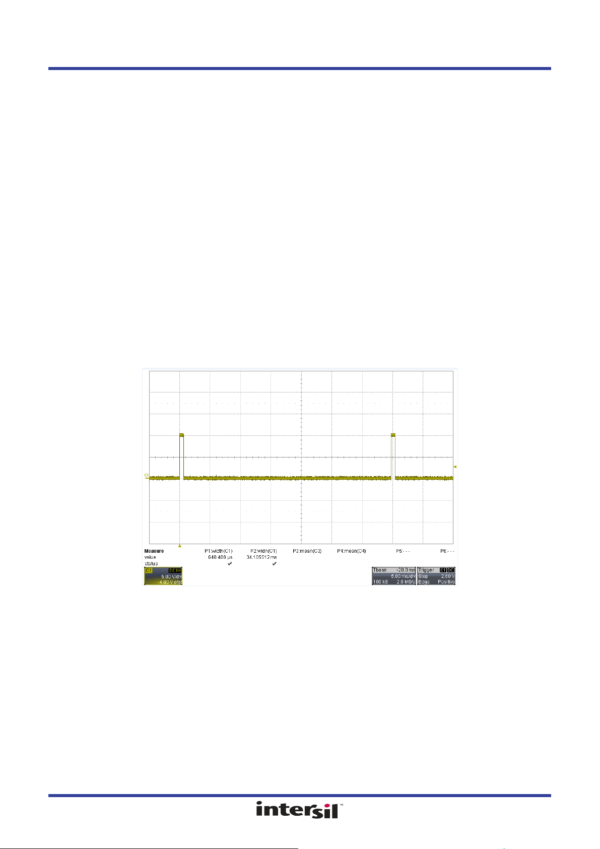
1.7 Using the Buck Regulator Transient Load Generator
An on-board load transient generator is made available to the buck regulator output. This circuit is shown in
Figure 7
N-MOSFET driver. The HIP2100 requires 10V bias applied between TP9 (positive) and TP5 (GND) for proper
operation. The load current is set by a resistance R
voltage B_OUT. Six 2512 sized resistor SMD pads (R32-R34; R40-R42) are made available for you to connect the
desired resistance.
and comprises of an open-drain active NMOS FET load switch driven by a Renesas HIP2100
inserted between the NMOS drain and buck output
LOAD
R12UZ0064EU0101 Rev.1.01 Page 6 of 23
Jan.6.20
Page 7
ISL70005SEHEV2Z 1. Functional Description
To control the load transient timing with an external signal, put switch SW3 in the down position (2-3). Connect the
external pulse generator to the JP5 2-pin header. The HIP2100 uses TTL inputs and requires 0V-10V signal
levels. Logic high drives the load on and logic low turns off the load.
The HIP2100 can be configured in an a-stable oscillation state where the load current is periodically pulsed, with
the transient duration set by RC timing components. To set the HIP2100 in a-stable state, ensure switch SW3 is in
the up position (1-2). In the first state, assume driver output HO = 0V, which turns MOSFET Q2 off. This allows
R28+R29 to charge up C34 with an RC time constant τ = (R28+R29) * C34. When the voltage across C34 (which
is connected to HI) reaches the logic high threshold of HI, HO goes into the second state and drives to a voltage
HO = VDD-0.7V. HO drives the Q3 MOSFET gate with turn-on (R30) and turn-off (R31) gate-limiting resistors.
When HO is high, Q3 is on and the buck output is loaded by the resistance across B_OUT and Q3 drain, with the
load current I
LOAD
=B_OUT/R
. At the same time when HO is high, Q2 is on discharging C34 through R29
LOAD
with RC time constant τ = R29 * C34. When the voltage across C34 reaches the logic low threshold of HI, HO = 0,
going back to its first state. Therefore, the transient load current interval is set by:
• Load Active: τ = R29*C34 to discharge C34/HI from V
• Load Inactive: τ = (R28+R29) * C34 to charge C34/HI from V
• The HIP2100 typical input thresholds are V
= 4.86V and VIL= 4.46V. The a-stable operation operates the
IH
to VIL of HIP2100.
IH
to VIH of HIP2100.
IL
HIP2100 between the hysteresis window of the HI input pin.
• The load active time with R29 = 1kΩ and C34 = 10µF is approximately 800µs.
• The load inactive time with R28 = 48.7kΩ, R29 = 1kΩ and C34 = 10µF is approximately 40ms.
Figure 3. A-Stable Transient Load Current Timing Control
1.8 Changing Output Voltage on LDO
The LDO output voltage is set by the equation: L_OUT = L_EA+ * (R21/R22 + 1)
There are three variables to control LDO output voltage. The L_EA+ voltage can be connected to the
ISL70005SEH VREF = 0.6V by setting the jumper in the 1-2 position of JP6 or to one-half of the buck output
voltage by setting the jumper in the 2-3 position. Additionally, you can put in an external reference by not having a
jumper on JP6 and applying a voltage to pin 2 of JP6 and GND. The ISL70005SEHEV2Z is preset with a
feedback gain of 2 with R21 = R22 = 1kΩ. You can populate jumper JP4 to short out R21 for unity gain feedback
to set L_OUT = L_EA+. You can also change the R21 and R22 resistor values for the desired feedback gain.
R12UZ0064EU0101 Rev.1.01 Page 7 of 23
Jan.6.20
Page 8

ISL70005SEHEV2Z 1. Functional Description
1.9 Using the LDO Regulator Transient Load Generator
To use the transient load generator for the LDO, first set up the board properly. JP9 must have a jumper installed.
For sourcing transient load, J2 must have a jumper. For sinking transient load, J1 must have a jumper. An external
voltage higher than L_OUT must be applied to load power (BA8) for sinking current.
An on-board load transient generator is made available to the LDO regulator output. This circuit is shown in
Figure 6
PMOS connected in a push-pull configuration to allow for sourcing and sinking current on the LDO. The source
and sink transient load currents are controlled by a single input on BNC1.
The sourcing circuit includes the lower NMOS FET Q1 and the resistor network R6//R35//R37. A 0V (off) to 5V
(on) signal from a signal generator is adequate to control the sourcing MOSFET Q1. When NMOS Q1 is on, the
LDO sourcing load current is I
with R35 and R37 as DNP.
The sinking circuit includes the upper PMOS FET Q1 and the resistor network R5//R27//R36. A 5V (off) to -5V
(on) signal from a signal generator is adequate to control the sinking MOSFET Q1. When PMOS Q1 is on, the
LDO sinking load current is ISINK = (LOAD_POWER – L_OUT) / (R5//R27//R36) where LOAD_POWER is the
external voltage applied to BA8. The ISL70005SEH is populated with R5 = 1Ω with R27 and R36 as DNP.
Note: R5 and R6 are 1W 2512 sized SMD resistors. When sourcing or sinking 1A, the power dissipation is at its
maximum rating.
(bottom left corner of the schematic) and is comprised of one open-drain NMOS and one open-drain
SOURCE
= L_OUT / (R6//R35//R37). The ISL70005SEH is populated with R6 = 1Ω
Note: When using the sinking load current circuit, if an external voltage less than L_OUT-0.7V is applied to
LOAD_POWER on terminal BA8, the LDO L_OUT can potentially source current through R5 and body-drain
diode of the Q1 PMOS even with zero gate-source voltage. Ensure that external voltage applied to BA8 is higher
than L_OUT to avoid back biasing the PMOS.
R12UZ0064EU0101 Rev.1.01 Page 8 of 23
Jan.6.20
Page 9

ISL70005SEHEV2Z 2. PCB Layout Guidelines
2. PCB Layout Guidelines
2.1 ISL70005SEHEV2Z Evaluation Board
Figure 4. ISL70005SEHEV2Z Evaluation Board (Top)
Figure 5. ISL70005SEHEV2Z Evaluation Board (Bottom)
R12UZ0064EU0101 Rev.1.01 Page 9 of 23
Jan.6.20
Page 10

RELEASED BY:
DRAWN
BY:
SHEET
HRDWR
ID
DATE:
DATE:
DATE:
TESTER
FILENAME:
MASK# REV.
DATE:ENGINEER:
TITLE:
UPDATED BY:
09/25/2019
B
TIM LOC
SCHEMATIC
EVALUATION BOARD
ISL70005SEH
2
TIM KLEMANN
1
GND
GND
GND
GND
IN
OUT
OUT
OUT
OUT
OUT
SW2
1
2
3
0.01UF
C5
R15
1K
TP14
0.1UF
C38
TP3
C10
1UF
R6
1
2512
2N7002E
Q4
C27
1UF
R35
DNP
2512
2N7002E
Q5
C18
0.1UF
B_LX1
B_PVIN1
B_GND2
L_GND2
L_VIN
L_OUT
L_PGND
L_GND1
L_EA-
VREF
B_EN
L_EN
L_VCC
L_SS
L_EA+
B_GND1
B_GND2
B_LX2
B_PVIN2
B_PG
L_PG
B_COMP
B_SS
B_GND1
B_SYNC
B_VCC
B_RT
B_FB
U1
ISL70005SEHVF
1
2
3
4
5
6
7
8
9
10
11
12
13
14 15
16
17
18
19
20
21
22
23
24
25
26
27
28
JP10
10K
R18
SW1
1
2
3
12
J4
0.1UF
C35
R4
45.3K
R11
10K
R5
1
2512
OPEN
C32
C39
7343-43
DNP
BA8
R27
DNP
2512
JP9
TP15
1K
R22
C25
10UF
0805
15UH
L1B
BA5
R3
36.5K
C9
150UF
7343-31
R25
1
R2
10K
JP3
C11
DNP
7343-43
BA7
2512
49.9
R16
TP17
0805
C20
10UF
TP10
1K
R21
7343-43
C17
150UF
10UF
0805
C37
C7
0.01UF
2.2UH
L1A
BA2
330PF
C1
R7
21.5K
D4
TP12
10K
R1
JP2
BA6
TP16
82PF
C3
R39
DNP
TP2
5.9K
R9
BA1
R12
10K
1UF
C22
R8
10K
1K
R23
TP8
10K
R20
D5
12
J5
R13
200K
0
R38
C24
0.1UF
150UF
C14
7343-43
JP6
1 2 3
12
J7
C2
0.1UF
0
R44
1UF
C15
0.1UF
C16
R37
DNP
2512
1K
R24
TP6
SI4599DY
Q1A
1
2
7
8
1000PF
C29
JP1
25K
R10
C19
DNP
7343-43
BA4
10K
R19
12
J3
C12
1UF
C4
1UF
150UF
C6
7343-43
150UF
7343-43
C36
R36
DNP
2512
12
J6
200K
R17
TP5
0.1UF
C21
Q1B
SI4599DY
3
4
5
6
JP4
1UF
C30
BNC1
390PF
C8
BA3
J2
12.4K
R43
R14
1K
TP13
TP4
C13
1UF
D1
TP1
D2
C31
0.1UF
OPEN
C23
J1
1000PF
C28
0.1UF
C26
B_COMP
B_EN
B_FB
B_OUT
B_PG
B_RT
B_SS
B_SYNC
LOAD_CONTROL
LOAD_POWER
LX
L_EA+
L_EN
L_OUT
L_PG
L_SS
L_VCC
L_VIN
PVIN
PVIN
PVIN
UNNAMED_1_2N7002_I755_D
UNNAMED_1_2N7002_I759_D
UNNAMED_1_GTSERIES_I702_NO
UNNAMED_1_GTSERIES_I703_NO
UNNAMED_1_ISL70005SEH_I603_PIN15
UNNAMED_1_ISL70005SEH_I603_PIN18
UNNAMED_1_JUMPER2_I620_IN1
UNNAMED_1_JUMPER2_I622_IN1
UNNAMED_1_JUMPER2_I657_IN1
UNNAMED_1_JUMPER2_I677_IN1
UNNAMED_1_JUMPER2_I708_IN1UNNAMED_1_JUMPER2_I709_IN2
UNNAMED_1_JUMPER3_I502_IN3
UNNAMED_1_SI4599_I579_D1A
UNNAMED_1_SI4599_I580_D2A
UNNAMED_1_SMCAP_I500_AUNNAMED_1_SMCAP_I500_B
UNNAMED_1_SMCAP_I581_B
UNNAMED_1_SMCAP_I664_B
UNNAMED_1_SMLEDWCOLOR_I754_A
UNNAMED_1_SMLEDWCOLOR_I758_A
VREF
R12UZ0064EU0101 Rev.1.01 Page 10 of 23
Jan.6.20
2.2 ISL70005SEHEV2Z Schematic
ISL70005SEHEV2Z 2. PCB Layout Guidelines
Figure 6. Schematic - Page 1
Page 11

R12UZ0064EU0101 Rev.1.01 Page 11 of 23
LOAD TRANSIENT GENERATOR
LOAD TRANSIENT ENABLE
12V EXTERNAL
IN
2512
DNP
R33
R29
1K
604
R30
TP9
2512
DNP
R34
D3
1
2
3
2512
DNP
R40
10UF
C33
2512
DNP
R41
C34
10UF
2512
DNP
R42
SW3
1
2
3
R26
10K
48.7K
R28
TP11
JP5
Q3
1
2
3
2N7002-7-F
Q2
R45
10K
2512
DNP
R32
HI
LO
HS
HO LI
VSS
VDD
HB
U8
1
2
3
4 5
6
7
8
R31
150
TP7
B_OUT
UNNAMED_7_2N7002_I39_D
UNNAMED_7_GTSERIES_I17_COM UNNAMED_7_GTSERIES_I17_NC
UNNAMED_7_GTSERIES_I17_NO
UNNAMED_7_HIP2100_I21_HB
UNNAMED_7_HIP2100_I21_HO
UNNAMED_7_SMRES_I40_B
UNNAMED_7_SMRES_I41_B
UNNAMED_7_SMRES_I64_B
VDIF2
Jan.6.20
ISL70005SEHEV2Z 2. PCB Layout Guidelines
Figure 7. Schematic - Page 2
Page 12

ISL70005SEHEV2Z 2. PCB Layout Guidelines
2.3 Bill of Materials
Qty Reference Designator Description Manufacturer Manufacturer Part
1PWB-PCB,
ISL70005SEHEV2Z, REVB,
ROHS
8 C4, C10, C12, C13, C15, C22,
C27, C30
3 C20, C25, C37 CAP, SMD, 0805, 10µF, 16V,
2 C28, C29 CAP, SMD, 0603, 1000pF, 16V,
2 C5, C7 CAP, SMD, 0603, 0.01µF, 16V,
9 C2, C16, C18, C21, C24, C26,
C31, C35, C38
1 C1 CAP, SMD, 0603, 330pF, 50V,
1 C8 CAP, SMD, 0603, 390pF, 50V,
1 C3 CAP, SMD, 0603, 82pF, 50V,
0 C23, C32 CAP, SMD, 0603, DNP-PLACE
2 C33, C34 CAP, SMD, 1206, 10µF, 16V,
5 C6, C9, C14, C17, C36 CAP-TANT, LOWESR, SMD,
1 L1A COIL-PWR INDUCTOR, SMD,
16 TP2-TP17 CONN-DBL TURRET, TH,
1 BNC1 CONN-BNC, RECEPTACLE,
1 TP1 CONN-MINI TEST POINT,
8 BA1-BA8 CONN-JACK, MINI BANANA,
1 JP6 CONN-HEADER, 1x3,
14 J1, J2, J3, J4, J5, J6, J7, JP1,
JP2, JP3, JP4, JP5, JP9, JP10
8 J1, J2, JP1, JP2, JP4, JP9,
JP10, JP6-Pins 2-3
2 D1, D2 DIODE-SCHOTTKY
CAP, SMD, 0603, 1.0µF, 16V,
10%, X7R, ROHS
20%, X7R, ROHS
10%, X7R, ROHS
10%, X7R, ROHS
CAP, SMD, 0603, 0.1µF, 16V,
10%, X7R, ROHS
10%, X7R, ROHS
10%, X7R, ROHS
10%, C0G, ROHS
HOLDER, ROHS
10%, X5R, ROHS
7.3x4.3mm, 150µF, 16V, 10%,
30mΩ, ROHS
4mm, 2.2µH, 20%, 3.5A,
21.3mΩ, ROHS
0.218x0.078 PCB MNT,
TIN/BRASS, ROHS
TH, 4 POST, 50Ω,
SILVERCONTACT, ROHS
VERTICAL, WHITE, ROHS
0.175 PLUG, NICKEL/BRASS,
ROHS
BREAKAWY 1x36, 2.54mm,
ROHS
CONN-HEADER, 1x2,
RETENTIVE, 2.54mm,
0.230x0.120, ROHS
CONN-JUMPER, SHORTING,
2PIN, BLACK, GOLD, ROHS
RECITIFIER, SMD, 2P, SMA,
20V, 1A, ROHS, DNP-PLACE
HOLDER
Imagineering Inc ISL70005SEHEV2ZREVBPCB
TDK C1608X7R1C105K
Taiyo Yuden EMK212BB7106MG-T
Venkel C0603X7R160102KNE
Venkel C0603X7R160-103KNE
Murata GCM188R71C104KA37D
Yageo CC0603KRX7R9BB331
Venkel C0603X7R500-391KNE
Venkel C0603COG500-820KNE
Venkel C1206X5R160-106KNE
(Pb-Free)
AVX TPME157K016R0030
Coilcraft XFL4020-222MEB
Keystone 1502-1
Amphenol 31-5329-51RFX
Keystone 5002
Keystone 575-4
BERG/FCI 68000-236HLF
BERG/FCI 69190-202HLF
Sullins SPC02SYAN
R12UZ0064EU0101 Rev.1.01 Page 12 of 23
Jan.6.20
Page 13

ISL70005SEHEV2Z 2. PCB Layout Guidelines
Qty Reference Designator Description Manufacturer Manufacturer Part
1 D3 DIODE-SCHOTTKY,
DUALDIODE, SMD, 3P, SOT23,
30V, 200mA, ROHS
2 D4, D5 LED-GaAs RED, SMD,
2X1.25mm, 100mW, 40mA,
10mcd, ROHS
1 U8 IC-HI FREQ BRIDGE DRIVER,
8P, SOIC, 100V, ROHS
1 U1 IC-RAD HARD LDO
1 Q2 TRANSISTOR, N-CHANNEL,
2 Q4, Q5 TRANSIST-MOS, N-CHANNEL,
1 Q1 TRANSISTOR-N/P CHANNEL,
1 Q3 TRANSISTOR-MOS,
1 R16 RES-AEC-Q200, SMD, 2512,
0 R39 RESISTOR, SMD, 0603, 0.1%,
1 R25 RES, SMD, 0603, 1Ω, 1/10W,
7 R14, R15, R21, R22, R23, R24,
R29
10 R1, R2, R8, R11, R12, R18,
R19, R20, R26, R45
1 R43 RES, SMD, 0603, 12.4k, 1/10W,
1 R31 RES, SMD, 0603, 150Ω, 1/10W,
2 R13, R17 RES, SMD, 0603, 200k, 1/10W,
1 R7 RES, SMD, 0603, 21.5k, 1/10W,
1 R10 RES, SMD, 0603, 24.9k, 1/10W,
1 R3 RES, SMD, 0603, 36.5k, 1/10W,
1 R4 RES, SMD, 0603, 45.3k, 1/10W,
1 R28 RES, SMD, 0603, 48.7k, 1/10W,
1 R9 RES, SMD, 0603, 5.90k, 1/10W,
1 R30 RES, SMD, 0603, 604Ω, 1/10W,
REGULATOR, SMD, 28P, CFP,
ROHS
3LD, SOT-23, 60V, 115mA,
ROHS
SMD, SOT23, 60V, 0.24A,
ROHS
8P, SOIC, 40V, 6.8/5.8A, ROHS
N-CHANNEL, SMD, TO-252,
30V, 90A, ROHS
49.9Ω, 1W, 1%, TF, ROHS
MF, DNP-PLACE HOLDER
1%, TF, ROHS
RES, SMD, 0603, 1k, 1/10W,
1%, TF, ROHS
RES, SMD, 0603, 10k, 1/10W,
1%, TF, ROHS
1%, TF, ROHS
1%, TF, ROHS
1%, TF, ROHS
1%, TF, ROHS
1%, TF, ROHS
1%, TF, ROHS
1%, TF, ROHS
1%, TF, ROHS
1%, TF, ROHS
1%, TF, ROHS
Fairchild BAT54S
Liteon/Vishay LTST-C170CKT
Renesas Electronics America HIP2100IBZ
Renesas Electronics America ISL70005SEHF/PROTO
Diodes, Inc. 2N7002-7-F
Vishay/Siliconix 2N7002E
Vishay/Siliconix SI4599DY-T1-GE3
Vishay SUD50N03-06AP-E3
Vishay/Dale CRCW251249R9FKEG
Panasonic ERJ-3RQF1R0V
Panasonic ERJ-3EKF1001V
Venkel CR0603-10W-1002FT
Venkel CR0603-10W-1242FT
(Pb-Free)
Venkel CR0603-10W-1500FT
Venkel CR0603-10W-2003FT
Venkel CR0603-10W-2152FT
Panasonic ERJ-3EKF2492V
Vishay CRCW060336K5FKEA
Yageo RC0603FR-0745K3L
Panasonic ERJ-3EKF4872V
Panasonic ERJ-3EKF5901V
Panasonic ERJ-3EKF6040V
R12UZ0064EU0101 Rev.1.01 Page 13 of 23
Jan.6.20
Page 14

ISL70005SEHEV2Z 2. PCB Layout Guidelines
Qty Reference Designator Description Manufacturer Manufacturer Part
2 R38, R44 RES, SMD, 0805, 0Ω, 1/8W, TF,
ROHS
2 R5, R6 RES, SMD, 2512, 1Ω, 1W, 1%,
0 R27, R32-R37, R40, R41, R42 RES, SMD, 2512, DNP, DNP,
3 SW1-SW3 SWITCH-TOGGLE, SMD,
4 Four corners SCREW, 4-40x1/4in, PHILLIPS,
4 Four corners STANDOFF, 4-40x3/4in, F/F,
0 C11, C19, C39
(TPME157K016R0030)
0 L1B (XAL6060-153MEC) DO NOT POPULATE OR
TF, ROHS
DNP, TF, ROHS
6PIN, SPDT, 2POS,
ON-NONE-ON, ROHS
PANHEAD, STAINLESS, ROHS
HEX, ALUMINUM, 0.25 OD,
ROHS
DO NOT POPULATE OR
PURCHASE
PURCHASE
Yageo RC0805JR-070RL
Vishay CRCW2512-1R00F
ITT Industries/C&K Division GT11MSCBE
Building Fasteners PMSSS 440 0025 PH
Keystone 2204
2.4 Board Layout
Figure 8. Silkscreen Top Layer
R12UZ0064EU0101 Rev.1.01 Page 14 of 23
Jan.6.20
Page 15

ISL70005SEHEV2Z 2. PCB Layout Guidelines
Figure 9. Top Layer
Figure 10. Layer 2
R12UZ0064EU0101 Rev.1.01 Page 15 of 23
Jan.6.20
Page 16

ISL70005SEHEV2Z 2. PCB Layout Guidelines
Figure 11. Layer 3
Figure 12. Layer 4
R12UZ0064EU0101 Rev.1.01 Page 16 of 23
Jan.6.20
Page 17

ISL70005SEHEV2Z 2. PCB Layout Guidelines
Figure 13. Silkscreen Bottom Layer
R12UZ0064EU0101 Rev.1.01 Page 17 of 23
Jan.6.20
Page 18

ISL70005SEHEV2Z 3. Typical Performance Curves
50
55
60
65
70
75
80
85
90
95
0.0 0.5 1.0 1.5 2.0 2.5
3.0
Efficiency (%)
Load Current (A)
Vout = 1.8V
50
55
60
65
70
75
80
85
90
95
0.0 0.5 1.0 1.5 2.0 2.5
3.0
Efficiency (%)
Load Current (A)
Vout = 3.3V
Vout = 2.5V
Vout = 1.8V
SS 500mV/Div
PG 2V/Div
VOUT 1V/Div
EN 5V/Div
500µs/DIV
SS 500mV/Div
PG 2V/Div
VOUT 1V/Div
EN 5V/Div
200µs/DIV
SS 1V/Div
PG 2V/Div
VOUT 1V/Div
EN 5V/Div
500µs/DIV
SS 1V/Div
PG 2V/Div
VOUT 1V/Div
EN 5V/Div
500µs/DIV
3. Typical Performance Curves
Unless otherwise noted, the test platform is the ISL70005SEHEV2Z where B_PVIN = B_VCC = L_VCC = 5V; L_VIN = 3V; B_OUT = 1.8V;
f
= 1MHz; Buck CIN= 150µF tantalum + 2x1µF ceramic; Buck C
SW
tantalum + 11µF ceramic; LDO C
= 150µF tantalum +12µF ceramic; L_OUT = 1.2V; L_EA+ = VREF = 0.6V; TA= +25°C.
OUT
= 150µF tantalum + 2x1µF ceramic; L
OUT
= 2.2µH; LDO CIN= 150µF
OUT
Figure 14. Efficiency vs I
; B_VIN = 3V; 1MHz Figure 15. Efficiency vs I
OUT
; B_VIN = 5V; 1MHz
OUT
Figure 16. Buck Soft-Start; Load = 0.68Ω; LDO Disabled Figure 17. Buck Soft-Start; Load = 0.68Ω; LDO Enabled
Figure 18. LDO Soft-Start; Load = 1.5Ω to GND; Buck
Disabled
R12UZ0064EU0101 Rev.1.01 Page 18 of 23
Jan.6.20
Figure 19. LDO Soft-Start; Load = 1.5Ω to GND; Buck
Enabled
Page 19

ISL70005SEHEV2Z 3. Typical Performance Curves
B_PG 2V/Div
B_VOUT 1V/Div
B_SS 1V/Div
EN 5V/Div
L_SS 1V/Div
L_PG 2V/Div
L_VOUT 1V/Div
500µs/Div
LX 5V/Div
1µs/Div
VOUT 50mV/Div
Inductor Current 500mA/Div
LX 5V/Div
1µs/Div
VOUT 50mV/Div
Inductor Current 500mA/Div
1.18
1.19
1.20
1.21
1.22
1.23
-1.5 -1.0 -0.5 0.0 0.5 1.0
1.5
Output Voltage (V)
Load Current (A)
L_VIN = 3V
L_VCC = B_VCC = 5V
L_EA+ = VREF
1% Resistor Divider
1.78
1.79
1.80
1.81
1.82
1.83
1.84
-1.5 -1.0 -0.5 0.0 0.5 1.0 1.5
Output Voltage (V)
Load Current (A)
L_VIN = 3V
L_VCC = B_VCC = 5V
L_EA+ = VREF
1% Resistor Divider
Unless otherwise noted, the test platform is the ISL70005SEHEV2Z where B_PVIN = B_VCC = L_VCC = 5V; L_VIN = 3V; B_OUT = 1.8V;
f
= 1MHz; Buck CIN= 150µF tantalum + 2x1µF ceramic; Buck C
SW
tantalum + 11µF ceramic; LDO C
= 150µF tantalum +12µF ceramic; L_OUT = 1.2V; L_EA+ = VREF = 0.6V; TA= +25°C. (Continued)
OUT
Figure 20. Buck and LDO Soft-Start; B_EN = L_EN; 0.68Ω Load on Buck; 1.5Ω Load on LDO; FPGA Configuration
= 150µF tantalum + 2x1µF ceramic; L
OUT
= 2.2µH; LDO CIN= 150µF
OUT
Figure 21. Buck Steady State Operation; Load = 0A Figure 22. Buck Steady State Operation; Load = 3A
R12UZ0064EU0101 Rev.1.01 Page 19 of 23
Jan.6.20
Figure 23. LDO Load Regulation Av = 2 Figure 24. LDO Load Regulation Av = 3
Page 20

ISL70005SEHEV2Z 3. Typical Performance Curves
1.150
1.155
1.160
1.165
1.170
1.175
1.180
1.185
1.190
1.23 1.24 1.25 1.26 1.27 1.28 1.29
L_VOUT Voltage (V)
L_VIN Voltage (V)
L_VCC = B_VCC = 5V
L_OUT = 1.2V;
1A Sourcing
Av = 2; L_EA+ = VREF
1.150
1.155
1.160
1.165
1.170
1.175
1.180
1.185
1.190
1.195
1.200
1.24 1.25 1.26 1.27 1.28 1.29 1.30
L_VOUT Voltage (V)
L_VIN Voltage (V)
L_VCC = B_VCC = 5V
L_OUT = 1.2V;
1A Sourcing
Av = 1; L_EA+ = 1.2V
Unless otherwise noted, the test platform is the ISL70005SEHEV2Z where B_PVIN = B_VCC = L_VCC = 5V; L_VIN = 3V; B_OUT = 1.8V;
f
= 1MHz; Buck CIN= 150µF tantalum + 2x1µF ceramic; Buck C
SW
tantalum + 11µF ceramic; LDO C
= 150µF tantalum +12µF ceramic; L_OUT = 1.2V; L_EA+ = VREF = 0.6V; TA= +25°C. (Continued)
OUT
Figure 25. LDO Dropout Voltage; Av = 2 Figure 26. LDO Dropout Voltage; Av = 1
= 150µF tantalum + 2x1µF ceramic; L
OUT
= 2.2µH; LDO CIN= 150µF
OUT
R12UZ0064EU0101 Rev.1.01 Page 20 of 23
Jan.6.20
Page 21

ISL70005SEHEV2Z 4. Revision History
4. Revision History
Rev. Date Description
1.01 Jan.6.20 Changed diode D1 and D2 in BOM to DNP.
1.00 Dec.11.19 Initial release
R12UZ0064EU0101 Rev.1.01 Page 21 of 23
Jan.6.20
Page 22

IMPORTANT NOTICE AND DISCLAIMER
RENESAS ELECTRONICS CORPORATION AND ITS SUBSIDIARIES (“RENESAS”) PROVIDES TECHNICAL
SPECIFICATIONS AND RELIABILITY DATA (INCLUDING DATASHEETS), DESIGN RESOURCES (INCLUDING
REFERENCE DESIGNS), APPLICATION OR OTHER DESIGN ADVICE, WEB TOOLS, SAFETY INFORMATION, AND
OTHER RESOURCES “AS IS” AND WITH ALL FAULTS, AND DISCLAIMS ALL WARRANTIES, EXPRESS OR IMPLIED,
INCLUDING, WITHOUT LIMITATION, ANY IMPLIED WARRANTIES OF MERCHANTABILITY, FITNESS FOR A
PARTICULAR PURPOSE, OR NON-INFRINGEMENT OF THIRD PARTY INTELLECTUAL PROPERTY RIGHTS.
These resources are intended for developers skilled in the art designing with Renesas products. You are solely responsible
for (1) selecting the appropriate products for your application, (2) designing, validating, and testing your application, and (3)
ensuring your application meets applicable standards, and any other safety, security, or other requirements. These
resources are subject to change without notice. Renesas grants you permission to use these resources only for
development of an application that uses Renesas products. Other reproduction or use of these resources is strictly
prohibited. No lic ense is granted to any other Renesas intellectual property or to any third party intellectual property.
Renesas disclaims responsibility for, and you will fully indemnify Renesas and its representatives against, any claims,
damages, costs, losses, or liabilities arising out of your use of these resources. Renesas' products are provided only subject
to Renesas' Terms and Conditions of Sale or other applicable terms agreed to in writing. No use of any Renesas resources
expands or otherwise alters any applicable warranties or warranty disclaimers for these produc ts.
Corporate Headquarters
TOYOSU FORESIA, 3-2-24 Toyosu,
Koto-ku, Tokyo 135-0061, Japan
www.renesas .com
Trademarks
Renesas and the Renesas logo are trademarks of Renesas
Electronics Corporation. All trademarks and registered
trademarks are the property of their respective owners.
(Rev.1.0 Mar 2020)
Contact Information
For further information on a product, technology, the most
up-to-date version of a document, or your nearest sales
office, please visit:
www.renesas .com/contact/
© 2020 Renesas Electronics Corporation. All rights reserved.
Page 23

ISL70005SEHEV2Z
Renesas Electronics Corporation
www.renesas.com
R12UZ0064EU0101
 Loading...