

Page 1
USER’S MANUAL
ISL59481EVAL1
Evaluation Board User’s Guide
Introduction
The ISL59481EVAL1 evaluation board contains the ISL59481
Dual 4:1 RGB MUX amp and associated components needed
to implement an 8:1 RGB+H/V sync video multiplexer. The 8
video input ports, and single output port are accessed using
standard 15 pin VGA female connectors. The I/O connectors
are compatible with most VGA, SVGA and XGA video
sources and video monitors with VGA cable interfaces. A
typical application would use the ISL59481EVAL1 board to
multiplex anywhere from 2 to 8 PC’s or laptops to a single
video monitor or projector.
Evaluation Board Description and Key Features
The multiplexing of the RGB video is performed by the
ISL59481. Multiplexing the H and V sync signals is
accomplished using two ISL84051 8:1 analog switches. The
ISL59481 Video MUX and the analog H and V sync
multiplexers have the same input channel select logic
coding, and are parallel-connected to form a single 3 input
binary coded interface (S0, S1, S2). The evaluation board
contains three different channel select options via jumpers
on the board. Switches on the board enable direct logic
control in binary format. The on-board oscillator and 4-bit
counter can be connected to provide a continuous channel-
AN1235
Rev 0.00
Feb 2, 2006
by-channel scan of as few as 2 input channels up to all 8. An
added option allows the user to disconnect the auto-scan
oscillator and use the on-board momentary-contact switch to
manually scan through the selected channels.
Reference Documents
• ISL59481 Data Sheet, FN7456
Getting Started
The evaluation board should have the same appearance as
the silk screen shown in Figure 1. Prior to applying power,
connect the source input VGA cables and the evaluation
board output VGA cable to the respective video
components. The evaluation board, as supplied, is designed
for 75 source impedances and requires a 75 termination
impedance in the output display device.
Applying Power to the Evaluation Board
The following safeguards will ensure correct power-up.
1. Limit the current on ±5V supplies to 250mA.
2. Turn on the power supplies after the power cables are
attached to the evaluation board.
Power supply protection Schottky diodes are included on the
±5V supplies to prevent damage due to reverse polarity.
Evaluation Board Jumper, Cable Header, and Switch Descriptions
COMPONENT DESCRIPTION
JUMPERS
J1 Selects channel select via single-step momentary contact switch S4, or auto mode using on-board oscillator
J-S0 Selects S0 logic input to manual control via switch S0 or through external control ribbon cable header
J-S1 Selects S1 logic input to manual control via switch S1 or through external control ribbon cable header
J-S2 Selects S2 logic input to manual control via switch S2 or through external control ribbon cable header
HEADERS
EN External MUX enable: Internal pull-down (logic 0) enables RGB+H/V output, logic high disables RGB and H/V sync output
S0 External S0 channel select logic input
S1 External S1 channel select logic input
S2 External S2 channel select logic input
SWITCHES
S0 Manual channel select logic input S0
S1 Manual channel select logic input S1
S2 Manual channel select logic input S2
S3 Momentary contact channel select step control
AN1235 Rev 0.00 Page 1 of 7
Feb 2, 2006
Page 2

ISL59481EVAL1
FIGURE 1. ISL59481EVAL1 TOP VIEW
Testing the Evaluation Board
Testing the video and sync signal paths is accomplished
using 1 or more RGB+H/V test video sources and a video
monitor as the measurement device. Before powering the
board, connect the jumpers as follows:
AN1235 Rev 0.00 Page 2 of 7
Feb 2, 2006
1. Connect jumpers J-S0, J-S1 and J-S2 to the MANUAL
position (center to right post).
2. Connect jumper J1 to the single-step position (center to
left post).
Page 3
ISL59481EVAL1
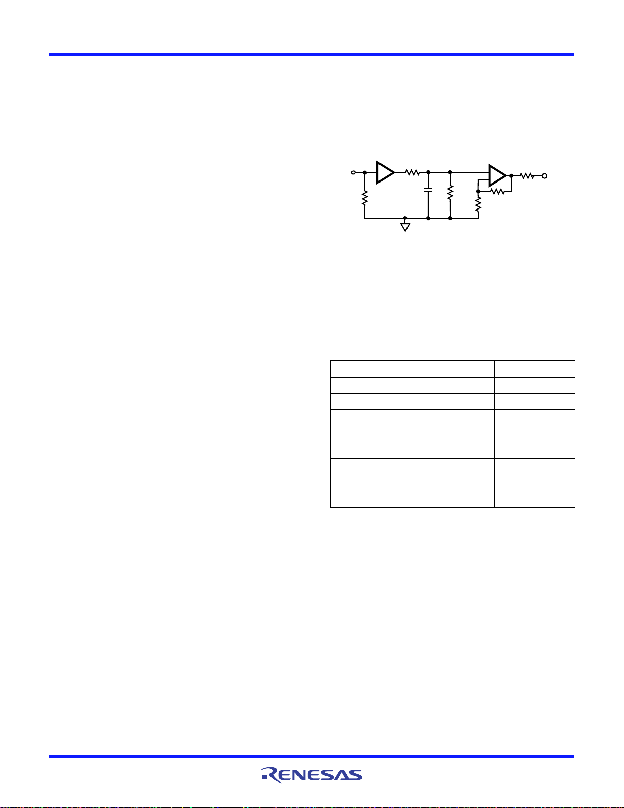
ISL59481
V
IN
75
Cnp*
RS, 75
+
-
1/3 EL5364
75
+1
V
OUT
R
f
R
g
Rt,
* Cnp is not populated and is provided for
frequency response adjustment
562
432
499
The following tests should be performed in the order shown.
Power Supply Tests
1. Connect an ammeter in series with the +5V and -5V
supply.
2. Connect power supplies to the respective +5V, -5V and
ground banana jacks.
3. Set supplies to +5V; ±50mV and -5V; ±50mV. Supply
power to the board.
4. Measure +5V supply current = +110mA ±20mA
5. Measure -5V supply current = -100mA ±20mA
Channel Select Logic and Video Performance Test
1. Calibrate the video test source with the video monitor by
connecting the source(s) to the video monitor and
selecting a display suitable for verifying correct
luminance, display resolution and H/V sync lock. The test
display in the following evaluation board tests should be
identical to the test display.
2. Re-connect the video monitor to the VIDEO_OUT VGA
connector on the evaluation board.
3. Connect the video test source to IN0. Additional video
sources can speed up the verification process. If more
than 1 test source is available connect each in sequential
fashion to IN1, IN2 etc.
4. Set switches S0, S1 and S2 to the GND position and
apply power.
5. After ~3s the test display supplied to IN0 should appear
on the test monitor exactly as it appeared in step 1.
NOTE: The ~3s delay is a built in delay common in many display
devices to lock onto the H/V sync signals and adjust the picture prior
to enabling the display screen.
6. Perform the display test on the remaining video inputs by
moving the video input source to the appropriate input
according to the truth table in Table 1.
Auto-Scan Test
1. Connect scope probe to the J1 AUTO pin and observe a
logic level (0 to +5V) square wave with ~3s period.
2. Connect jumpers J-S0, J-S1, and J-S2 to the AUTO
position (center to left post).
3. Connect jumper J1 to the AUTO position and observe
that the display scans all the test sources connected to
the input channels (center to right post).
4. Connect jumper J1 to the single-step position and use the
momentary contact switch S4 to manually all the test
sources.
Test completed.
RGB Video Signal Path
The video inputs are terminated with 75 resulting in an
overall RGB video path gain of 1 when using 75 video
source impedance and load terminations (Figure 2). The
RGB outputs contain series-connected 75 backtermination resistors for cable driving. The ISL59481
operates in unity gain, and the EL5364 triple op amp gain is
AN1235 Rev 0.00 Page 3 of 7
Feb 2, 2006
set to 2.3 to compensate for the interstage and output
impedance matching loss. Two methods of gain adjustment
are provided. Increasing gain to compensate for cable
attenuation can be accomplished using the EL5364 R
R
gain resistors. Gain reduction is best achieved using the
g
divider network R
and Rt. Capacitor pads (Cnp) are
s
and
f
provided to adjust the frequency response of the amplifier.
FIGURE 2. VIDEO SIGNAL PATH
Channel Select Logic
The ISL59481 RGB MUX and the H/V sync MUX share the
same 1 of 8 input channel select logic inputs (S0, S1, S2).
The channel select logic is shown in Table 1. Three methods
of channel select logic control are provided using jumpers.
TABLE 1. CHANNEL SELECT TRUTH TABLE
S2 S1 S0 VIDEO OUT
000 IN0
001 IN1
010 IN2
011 IN3
100 IN4
101 IN5
110 IN6
111 IN7
Auto Sequencing Using the On-Board
Oscillator
An on-board 0.3Hz R-C oscillator (Figure 3) drives the
master clock of the 4-bit binary counter, which generates the
channel select logic inputs S0, S1 and S2. The default 6s
channel scan rate provides the time needed by the display to
sync-lock and adjust the picture prior to enabling the display.
The 2.2M(R1) resistor value can be reduced to speed up
the channel scan time. Jumper J1 is provided to select either
the 6s auto-step timer, or the momentary contact switch for
manual stepping.
Page 4

ISL59481EVAL1
U4C
5
6
R1
J1
S4
C1
AUTOSTEP
SINGLESTEP
TO BINARY
COUNTER CLK
MOMENTARY
CONTACT SWITCH
2.2M
1µF
channel scan is enabled. The MANUAL position connects the
on-board SPDT switches (S0, S1, and S2) for manual
selection. A parallel-connected EXTERNAL CONTROL ribbon
cable header is provided for external channel select control.
A wide range of auto-scan options can be selected by
connecting only 1 or 2 of the 3 jumpers to the internal logic,
with the remainder connected to the switch. For example,
connecting jumper J-S0 to the AUTO position and connecting
jumpers J-S1 and J-S2 to the MANUAL position with the
switches S1 and S2 to the logic 0 state limits the channel scan
to only 2 of the 8 channels (IN0 and IN1). Moving a second
jumper from the MANUAL position to the AUTO position,
FIGURE 3. CHANNEL SCAN OSCILLATOR
Internal and External Channel Select Logic
J-S0, J-S1 and J-S2 are two-position jumpers that control the
method of channel selection. In the AUTO position, the internal
TABLE 2. CHANNEL SCAN SELECT LOGIC TABLE
CHANNELS
SCANNED
8 AutoAutoAuto- - - XXXXXXXX
4 Manual Auto Auto 0 - - X X X X
2 Manual Manual Auto 0 0 - X X
JUMPER POSITION SWITCH POSITION CHANNELS SELECTED
J-S2 J-S1 J-S0 S2 S1 S0 IN0 IN1 IN2 IN3 IN4 IN5 IN6 IN7
Manual Auto Auto 1 - - X X X X
Auto Manual Auto - 0 - X X X X
Auto Manual Auto - 1 - X X X X
Auto Auto Manual - - 0 X X X X
Auto Auto Manual - - 1 X X X X
Manual Manual Auto 0 1 - X X
Manual Manual Auto 1 0 - X X
Manual Manual Auto 1 1 - X X
Auto Manual Manual - 0 0 X X
Auto Manual Manual - 0 1 X X
Auto Manual Manual - 1 0 X X
Auto Manual Manual - 1 1 X X
Manual Auto Manual 0 - 0 X X
Manual Auto Manual 0 - 1 X X
Manual Auto Manual 1 - 0 X X
Manual Auto Manual 1 - 1 X X
increases the number of channels scanned from 2 to 4. The
complete list of channel scan jumper options are shown in
Table 2.
AN1235 Rev 0.00 Page 4 of 7
Feb 2, 2006
Page 5

ISL59481EVAL1
1 OUTC1
2 OUTB1
4 OUTA1
6 EN1
7 HIZ1
8
9 IN0B1
10 IN0A1
11 G ND
12 IN1A1
24 OUTA2
21 OUTC2
U1
5 V1+
IN0C1
22 OUTB2
23 V2-
13 IN2B2
14 IN2C2
15 GND
16 IN3A2
20 S0-2
19 S1-2
18 IN3C2
17 IN3B2
3 V1-
IN2A2 36
GND 35
IN1B2 33
GND 31
IN0A2 30
IN0B2 29
IN0C2 28
HIZ2 27
EN2
26
V2+ 25
IN1A2 32
IN1C2 34
SO-1 48
S1-1 47
IN3B1 45
GND 43
IN2C1 42
IN2B1 41
IN2A1 40
GND 39
IN1C1 38
IN1B1 37
IN3A1 44
IN3C1 46
1
2
4
6
7
8
9
10
11
12
5
3
13
14
15
Video Out
Input IN6
(IN2X2)
Input IN0
(IN0X1)
Input IN7
(IN3X2)
Input IN4
IN0X2
Input IN5
IN1X2
Input IN1
(IN1X1)
Input IN2
(IN2X1)
14
15
16
9
13
12
11
10
1
2
3
4
5
7
6
8
NO1
NO3
COM
NO7
NO5
INH
GND
V-
V+
NO4
NO0
NO6
ADDC
ADDB
ADDA
NO2
LOGIC
N.C.
N.C.
N.C.
N.C.
N.C.
1
2
4
6
7
8
9
10
11
12
5
3
13
14
15
N.C.
N.C.
N.C.
N.C.
N.C.
1 2 4 6 7 89
10
11
12
5
3
131415
N.C.
N.C.
N.C.
N.C.
N.C.
1 2 4 6 7 89
10
11
12
5
3
131415
N.C.
N.C.
N.C.
N.C.
N.C.
1
2
4
6
7
8
9
10
11
12
5
3
13
14
15
N.C.
N.C.
N.C.
N.C.
N.C.
1
2
4
6
7
8
9
10
11
12
5
3
13
14
15
N.C.
N.C.
N.C.
N.C.
N.C.
N.C.
N.C.
N.C.
N.C.
N.C.
14
15
16
9
13
12
11
10
1
2
3
4
5
7
6
8
NO1
NO3
COM
NO7
NO5
INH
GND
V-
V+
NO4
NO0
NO6
ADDC
ADDB
ADDA
NO2
LOGIC
0
V-SY NC
H-SYNC
H-Sync
V-Syn c
R
G
B
H-Sync
V-Syn c
R
G
B
H-Sync
V-Syn c
R
G
B
H-Sync
V-Sy nc
R
G
B
H-Sync
V-Sy nc
RGB
1 2 4 6 7 89
10
11
12
5
3
131415
N.C.
N.C.
N.C.
N.C.
N.C.
H-Sync
V-Syn c
RGB
1 2 4 6 7 89
10
11
12
5
3
131415
N.C.
N.C.
N.C.
N.C.
N.C.
H-Sync
V-Sy nc
RGB
1 2 4 6 7 89
10
11
12
5
3
131415
H-Sync
V-Sy nc
RGB
H-Sync
V-Sy nc
RGB
V+ (+5V)
V- ( -5V)
ISL59481
U2
U3
U4F
GND
EN
ISL84051
ISL84051
U4A
U4B
U4D
U4E
1
2
3
4
9
8
11
10
7
14 V+
V+
RCO 15
QA 14
QB 13
QC 12
U4C
13 12
QD 11
1 Reset
2 CLK
3 P0
9 LD
10 ENT
4 P1
5 P2
6 P3
7 ENP
16 V+
8 GND
GND
5
6
74HC14D
74HC161D
U5
2.2M
J-S0
J-S1
J-S2
S0
S1
S2
J1
S4
1µF
EN
S0
S1
S2
V+
4.7k
4.7k
4.7k
75
75
75
75
75
75
75
75
NP
75
75
75
75
75
75
10k
75
75
NP
NP
10k
75
75
75
75
75
75
75
75
75
75
75
75
75
75
75
75
0
0
0
0
4.7k
4.7k
4.7k
4.7k
10k
0
10k
10k
10k
IN3-R
IN3-G
IN3-B
IN2A2
IN2B2
IN2C2
IN2-R
IN2-G
IN2-B
IN3A2
IN3B2
IN3C2
IN6-R
IN1C1
IN1B1
IN1A1
IN6-G
IN6-B
IN2C1
IN2B1
IN2A1
IN3-R
IN3-G
IN3-B
Input IN3
(IN3X1)
IN1-R
IN1-G
IN1-B
IN0C1
IN0B1
IN0A1
75
IN3C1
IN3B1
IN3A1
IN5-B
IN5-G
IN5-R
IN4-R
IN4-G
IN4-B
IN0-B
IN0-G
IN0-R
Singlestep
Autostep
Auto
Manual
External
Control
U4A
U6A
U6B
U6C
0
562
432
432
562
562
432
0
NP
NP
EL5364
+
-
+
-
+
-
499
499
499
75
ISL59481EVAL1 Schematic Diagram
AN1235 Rev 0.00 Page 5 of 7
Feb 2, 2006
Page 6

ISL59481EVAL1
ISL59481EVAL1 Components List
COMPONENT VALUE TOLERANCE RATING COMPONENT VALUE TOLERANCE RATING
PWB ISL59481EVAL1RE
VA PCB
U
- 8:1 RGB Video
1
MUX
U
, U3 - 8:1 Analog
2
MUX
U
- Hex Inverter SN74HC14D
4
U
- 4-Bit Binary
5
Counter
- Triple 600MHz
U
6
CFA Op Amp
C4, C7 CAP, SMD, 0603
C2, C5, C8-C13,
C21, C22
C3, C6 CAPACITOR, SMD,
C1 CAPACITOR, SMD,
C14-C20 CAPACITOR, SMD,
IN0-IN7,
VIDEO_OUT
+5V, -5V, EN, GND CONN-JACK,
J2 CONN-HEADER,
ISL59481IRZA
QFN48 Pb-Free
ISL84051IBZ
SOIC16 Pb-Free
SOIC14
SN74HC161D
SOIC16
EL5364ISZ SOIC16
Pb-Free
1000pF
CAPACITOR, SMD,
0603, 0.1µF
0805, 10µF
0805, 2.2µF
0805, DNP-PLACE
HOLDER
CONN-SUB MINI D,
15PIN,
RECEPTACLE, RT
ANGLE, FRONT
METAL SHELL
BANA-SSSDRLESS, VERTIC
4PIN, BRKAWY,
2.54mm, VERTICAL
Intersil Corp. N/A J-S0, J-S1, J-S2, J1 CONN-HEADER,
1x3, BRKAWY
1X36, 0.1
Intersil Corp. N/A D1, D2 DIODE-
RECTIFIER, SMD
SOD-123, 2PIN
Intersil Corp. N/A R3-R5, R55-58, R64-R66 RESISTOR, SMD,
0805, DNP, DNP,
DNP, TF
N/A N/A R10-R12 RESISTOR, SMD,
0603, 75
N/A N/A R62, R67, R73 RESISTOR, SMD,
0603, 432
Intersil Corp. N/A R63, R71, R72 RESISTOR, SMD,
10%, X7R 25V R6-R9, R16, R21-R29,
R32, R35, R38, R43-R49
N/A 25V R13-R15, R17-R20, R33,
R34, R39, R68-R70
10%, X5R 6.3V R42, R50-R54. RESISTOR, SMD,
10%, X5R 16V R1 RESISTOR, SMD,
N/A N/A R2, R30, R31, R36, R37,
R40, R41
N/A N/A R59, R60, R61 RESISTOR, SMD,
N/A N/A S0-S2 SWITCH-
J2 S3 SWITCH-
0603, 562
RESISTOR, SMD,
0805, 75,
RESISTOR, SMD,
0805, 0,
0805, 10k
0805, 2.2M
RESISTOR, SMD,
0805, 4.7k
0805, 499
TOGGLE, THRU,
SPDT, 5 P, ON-N
PUSHBUTTON,
TH, 6mm, 4P,
ON/OFF,
N/A N/A
N/A N/A
MBR0540T1-T 40V, 0.5A
N/A N/A
1% 0.10W
1% 0.10W
1% 1/10W
N/A 1/10W
5% 1/10W
5% 1/8W
5% 1/10W
5% 1/10W
N/A N/A
N/A 12V, 0.05A
AN1235 Rev 0.00 Page 6 of 7
Feb 2, 2006
Page 7

http://www.renesas.com
Refer to "http://www.renesas.com/" for the latest and detailed information.
Renesas Electronics America Inc.
1001 Murphy Ranch Road, Milpitas, CA 95035, U.S.A.
Tel: +1-408-432-8888, Fax: +1-408-434-5351
Renesas Electronics Canada Limited
9251 Yonge Street, Suite 8309 Richmond Hill, Ontario Canada L4C 9T3
Tel: +1-905-237-2004
Renesas Electronics Europe Limited
Dukes Meadow, Millboard Road, Bourne End, Buckinghamshire, SL8 5FH, U.K
Tel: +44-1628-651-700, Fax: +44-1628-651-804
Renesas Electronics Europe GmbH
Arcadiastrasse 10, 40472 Düsseldorf, Germany
Tel: +49-211-6503-0, Fax: +49-211-6503-1327
Renesas Electronics (China) Co., Ltd.
Room 1709 Quantum Plaza, No.27 ZhichunLu, Haidian District, Beijing, 100191 P. R. China
Tel: +86-10-8235-1155, Fax: +86-10-8235-7679
Renesas Electronics (Shanghai) Co., Ltd.
Unit 301, Tower A, Central Towers, 555 Langao Road, Putuo District, Shanghai, 200333 P. R. China
Tel: +86-21-2226-0888, Fax: +86-21-2226-0999
Renesas Electronics Hong Kong Limited
Unit 1601-1611, 16/F., Tower 2, Grand Century Place, 193 Prince Edward Road West, Mongkok, Kowloon, Hong Kong
Tel: +852-2265-6688, Fax: +852 2886-9022
Renesas Electronics Taiwan Co., Ltd.
13F, No. 363, Fu Shing North Road, Taipei 10543, Taiwan
Tel: +886-2-8175-9600, Fax: +886 2-8175-9670
Renesas Electronics Singapore Pte. Ltd.
80 Bendemeer Road, Unit #06-02 Hyflux Innovation Centre, Singapore 339949
Tel: +65-6213-0200, Fax: +65-6213-0300
Renesas Electronics Malaysia Sdn.Bhd.
Unit 1207, Block B, Menara Amcorp, Amcorp Trade Centre, No. 18, Jln Persiaran Barat, 46050 Petaling Jaya, Selangor Darul Ehsan, Malaysia
Tel: +60-3-7955-9390, Fax: +60-3-7955-9510
Renesas Electronics India Pvt. Ltd.
No.777C, 100 Feet Road, HAL 2nd Stage, Indiranagar, Bangalore 560 038, India
Tel: +91-80-67208700, Fax: +91-80-67208777
Renesas Electronics Korea Co., Ltd.
17F, KAMCO Yangjae Tower, 262, Gangnam-daero, Gangnam-gu, Seoul, 06265 Korea
Tel: +82-2-558-3737, Fax: +82-2-558-5338
SALES OFFICES
© 2018 Renesas Electronics Corporation. All rights reserved.
Colophon 7.0
(Rev.4.0-1 November 2017)
Notice
1. Descriptions of circuits, software and other related information in this document are provided only to illustrate the operation of semiconductor products and application examples. You are fully responsible for
the incorporation or any other use of the circuits, software, and information in the design of your product or system. Renesas Electronics disclaims any and all liability for any losses and damages incurred by
you or third parties arising from the use of these circuits, software, or information.
2. Renesas Electronics hereby expressly disclaims any warranties against and liability for infringement or any other claims involving patents, copyrights, or other intellectual property rights of third parties, by or
arising from the use of Renesas Electronics products or technical information described in this document, including but not limited to, the product data, drawings, charts, programs, algorithms, and application
examples.
3. No license, express, implied or otherwise, is granted hereby under any patents, copyrights or other intellectual property rights of Renesas Electronics or others.
4. You shall not alter, modify, copy, or reverse engineer any Renesas Electronics product, whether in whole or in part. Renesas Electronics disclaims any and all liability for any losses or damages incurred by
you or third parties arising from such alteration, modification, copying or reverse engineering.
5. Renesas Electronics products are classified according to the following two quality grades: “Standard” and “High Quality”. The intended applications for each Renesas Electronics product depends on the
product’s quality grade, as indicated below.
"Standard": Computers; office equipment; communications equipment; test and measurement equipment; audio and visual equipment; home electronic appliances; machine tools; personal electronic
equipment; industrial robots; etc.
"High Quality": Transportation equipment (automobiles, trains, ships, etc.); traffic control (traffic lights); large-scale communication equipment; key financial terminal systems; safety control equipment; etc.
Unless expressly designated as a high reliability product or a product for harsh environments in a Renesas Electronics data sheet or other Renesas Electronics document, Renesas Electronics products are
not intended or authorized for use in products or systems that may pose a direct threat to human life or bodily injury (artificial life support devices or systems; surgical implantations; etc.), or may cause
serious property damage (space system; undersea repeaters; nuclear power control systems; aircraft control systems; key plant systems; military equipment; etc.). Renesas Electronics disclaims any and all
liability for any damages or losses incurred by you or any third parties arising from the use of any Renesas Electronics product that is inconsistent with any Renesas Electronics data sheet, user’s manual or
other Renesas Electronics document.
6. When using Renesas Electronics products, refer to the latest product information (data sheets, user’s manuals, application notes, “General Notes for Handling and Using Semiconductor Devices” in the
reliability handbook, etc.), and ensure that usage conditions are within the ranges specified by Renesas Electronics with respect to maximum ratings, operating power supply voltage range, heat dissipation
characteristics, installation, etc. Renesas Electronics disclaims any and all liability for any malfunctions, failure or accident arising out of the use of Renesas Electronics products outside of such specified
ranges.
7. Although Renesas Electronics endeavors to improve the quality and reliability of Renesas Electronics products, semiconductor products have specific characteristics, such as the occurrence of failure at a
certain rate and malfunctions under certain use conditions. Unless designated as a high reliability product or a product for harsh environments in a Renesas Electronics data sheet or other Renesas
Electronics document, Renesas Electronics products are not subject to radiation resistance design. You are responsible for implementing safety measures to guard against the possibility of bodily injury, injury
or damage caused by fire, and/or danger to the public in the event of a failure or malfunction of Renesas Electronics products, such as safety design for hardware and software, including but not limited to
redundancy, fire control and malfunction prevention, appropriate treatment for aging degradation or any other appropriate measures. Because the evaluation of microcomputer software alone is very difficult
and impractical, you are responsible for evaluating the safety of the final products or systems manufactured by you.
8. Please contact a Renesas Electronics sales office for details as to environmental matters such as the environmental compatibility of each Renesas Electronics product. You are responsible for carefully and
sufficiently investigating applicable laws and regulations that regulate the inclusion or use of controlled substances, including without limitation, the EU RoHS Directive, and using Renesas Electronics
products in compliance with all these applicable laws and regulations. Renesas Electronics disclaims any and all liability for damages or losses occurring as a result of your noncompliance with applicable
laws and regulations.
9. Renesas Electronics products and technologies shall not be used for or incorporated into any products or systems whose manufacture, use, or sale is prohibited under any applicable domestic or foreign laws
or regulations. You shall comply with any applicable export control laws and regulations promulgated and administered by the governments of any countries asserting jurisdiction over the parties or
transactions.
10. It is the responsibility of the buyer or distributor of Renesas Electronics products, or any other party who distributes, disposes of, or otherwise sells or transfers the product to a third party, to notify such third
party in advance of the contents and conditions set forth in this document.
11. This document shall not be reprinted, reproduced or duplicated in any form, in whole or in part, without prior written consent of Renesas Electronics.
12. Please contact a Renesas Electronics sales office if you have any questions regarding the information contained in this document or Renesas Electronics products.
(Note 1) “Renesas Electronics” as used in this document means Renesas Electronics Corporation and also includes its directly or indirectly controlled subsidiaries.
(Note 2) “Renesas Electronics product(s)” means any product developed or manufactured by or for Renesas Electronics.
 Loading...