

Page 1

USER’S MANUAL
FIGURE 1. EVALUATION BOARD SILK SCREEN
ISL5585XEVAL Evaluation Board User’s Guide
Introduction
The ISL55185XEVAL1 board can be used to evaluate the new
ISL5585 3.3volt SLIC. This platform supports the evaluation of
the performance of the ISL5585 at 3.3 volts with a 5 volt
CODEC. The lab data presented in this application note had
the following supplies voltages: Vcc (ISL5585) = 3.3V,
Vcc (CODEC) = 5V, VBH = -100v and Vbl = -24v.
The ISL5585XEVAL1 evaluation board provides a complete
evaluation system for the ISL5585 family of ringing SLICs.
Included on the evaluation board is a single +5V CODEC for
line circuit evaluations and on board logic for stand alone
operation. The evaluation boards have been designed to
support back to back operation, providing further insight to
the complete signal path and solution.
The transient behavior of the ISL5585 in response to mode
changes has been improved. The benefit to the application
is reduction or more likely elimination of DET
off hook events occur.
Voltage ratings for external components have been selected
based on 100V device operation, therefore compatibility to
lower voltage versions is guaranteed.
glitches when
AN1038
Rev 0.00
Sep 2002
Getting Started
Your evaluation kit should contain application note AN1038
and the following hardware.
1. One
2. One ISL5585X device sample, already in board.
3. One PLCC extraction tool.
4. One cable assembly with multi colored conductors.
5. One cable assembly with solid white conductors.
The evaluation board should have the same appearance as
the silk screen shown in Figure 1.
ISL5585XEVAL1evaluation board.
Applying Power to the Evaluation Board
Here are a few safeguards with power sequencing until you
are accustomed to using the high voltages required by the
devices.
1. Limit the current on all power supplies to 100mA.
2. Turn on the power supplies after the power cables are
attached to the evaluation boards.
AN1038 Rev 0.00 Page 1 of 14
Sep 2002
Page 2

ISL5585
APP CKT
CODEC
APP CKT
CLOCK GENERATION & MUX
JP1
JP2
JP3
JP4
JP5
JP6
JP7
JP8
JP9
JP10
JP11
JP12
J1
J2
J3
J4
J5 J6
J9
J10
J13
J14
J7 J8
J11
J12
J15
S1 S2 S3 S4 S5 S6
FIGURE 2. EVALUATION BOARD FUNCTIONAL DIAGRAM
Evaluation Board Functional Description
Evaluation Board Jumper Definitions
JUMPER DESCRIPTION
JP1 Connects SW- directly to the device Ring terminal of device. Used in conjunction with external load D
JP2 Connects SW+ through test load to the Tip terminal of device. Used in conjunction with external load D
JP3 Not used. Leave open.
JP4 Connects the receive output of the CODEC (U6) to the device receive input -IN. Path is AC coupled with C
JP5 Position1, CODEC: Connects the CODEC receive output to the device ringing input. Path is AC coupled by C
Position 2, EXT: Connects the VRS connector J9 to the device ringing input. Path is AC coupled by C
Position 3 TRAP: Connects the VRS connector J9 thru RC network to the device ringing input. Path is AC coupled.
JP6 Connects the device transmit output VTX to the CODEC amplifier for transhybrid balance. Path is AC coupled by C
JP7 Connects the receive output of CODEC to transhybrid amplifier, AC coupled by C
JP8 Inserting jumper sets the CODEC to A-law coding. Open sets the CODEC to -law coding.
JP9 Inserting jumper powers down the CODEC. Open provides normal CODEC operation.
JP10 Position 1: Sets the CODEC master clock to 2.048MHz.
Position 2: Sets the CODEC master clock to 512kHz
Position 3: Sets the CODEC master clock to 256kHz.
JP11 Enables the on board logic multiplexer. Should be installed for single board or back to back evaluations. Remove when driving
BNCs J10 thru J13.
JP12 Inserting jumper selects on board clock and frame sync generator. Insert to configure board as master for back to back
evaluations or for single board evaluations. Remove to configure board as slave for back to back evaluations.
. Normally inserted for proper operation.
1
and RTA.
TA
and RTA.
TA
.
RS
.
IN
RS
.
.
TX
AN1038 Rev 0.00 Page 2 of 14
Sep 2002
Page 3

Test Points
Each connector interface to the evaluation board has a test
point. All test points are DC coupled and should be guarded
against ground shorts. High impedance test inputs, such as
oscilloscopes or DVMs, should be used to monitor these
points. Unused BNC connections also provide convenient test
point access.
Toggle Switches
The six toggle switches, S1 thru S6, interface directly to the
ISL5585 device. Positioning any switch towards the top of the
board is a logic “1”. Positioning any switch towards the bottom
of the board is a logic “0”. All switches are labeled with the
control signal names.
The switch E0 selects the switch hook (E0 = 1) or the ground
key detector (E0 = 0) to appear at DET
device overrides E0 and sends the ring trip detector to DET
The switched labeled SWC
turns on the uncommitted switch
when set to a logic low. The battery select signal BSEL, selects
the high battery when set to logic high. The operating modes
for the ISL5585 device are provided in Table 1.
. During ringing, the
.
OPERATING MODE F2 F1 F0
Low Power Standby 0 0 0
Forward Active 0 0 1
Unused 0 1 0
Reverse Active 0 1 1
Ringing 1 0 0
Forward Loop Back (Note) 1 0 1
Tip Open 1 1 0
Power Denial 1 1 1
NOTE: The ISL5585 device should always operate from low battery
voltage when using the Forward Loop Back mode.
Refer to the device electrical data sheet for detailed
descriptions regarding each operating mode according to the
device under evaluation.
Evaluation Board Connector Descriptions
CONNECTOR DESCRIPTION
TABLE 1. ISL5585 OPERATING MODES
J1 RJ11 type phone connector.
J2 Ring terminal of board.
J3 Tip terminal of board.
J4 Grounding lug connected to board ground plane.
J5 1: V
J6 Identical pinout as J5. Either connector provides daisy chain connection to second board for back to back evaluation.
J7 Transmit analog output from ISL5585 device, VTX. This path is AC coupled by C
J8 Receive analog input to ISL5585 device, VREC. This path is AC coupled by C
J9 Ringing input to ISL5585 device, VRS. This path is AC coupled by C
J10 Serial transmit data output of CODEC U6.
J11 Serial receive data input to CODEC U6.
J12 Common frame sync input for receive and transmit digital data.
J13 Common clock for CODEC data transfer and conversion.
. Positive 5V supply to CODEC U6, clock generator U5 and logic devices U2 thru U4 (red wire).
CC
2: V
. High negative battery supply to the ISL5585 device (orange wire).
BH
3: V
. Low negative battery supply to the ISL5585 device (yellow wire).
BL
4: +5V. Positive 5V supply to the ISL5585 device and LEDs (green wire).
7 thru 10: GND. Twisted pair returns for external supply connections (black wires).
.
TX
.
IN
.
RS
J14 20 pin, 100 mil spacing header with all digital PCM data interfaces to CODEC U6.
J15 20 pin, 100 mil spacing header with all digital interfaces to ISL5585 device.
AN1038 Rev 0.00 Page 3 of 14
Sep 2002
Page 4

ISL5585
APP CKT
CODEC
APP CKT
CLOCK GENERATION & MUX
JP1
JP2
JP3
JP4
JP5
JP6
JP7
JP8
JP9
JP10
JP11
JP12
J1
J2
J3
J4
J5 J6
J9
J10
J14
J7 J8
J11
J12
J15
S1 S2 S3 S4 S5 S6
FIGURE 3. STAND ALONE CONNECTORS AND JUMPERS
5
FIGURE 4. TEST LOAD SWITCHING
RING
TIP
R
TA
D
TA
SW+
SW-
SWC
JP1
JP2
Stand Alone Configuration
Description
The standalone configuration supports any measurement of
the ISL5585 device. With all the jumper locations open, the
device is totally isolated from all other active circuitry on the
evaluation board. All other circuitry is powered, but does not
interfere with proper SLIC operation.
Power Supply Connections
Power should be applied to the evaluation board using the
primary power cable. Either J5 or J6 may be used. Prior to
applying power, the voltage setting of each supply should be
verified. The power supplies should be turned off while mating
the primary power cable to the evaluation board.
Jumper Settings
All jumper positions should be open for the stand alone
configuration.
Measurement Capability
Nearly all AC and DC parameters of the device can be
measured using this configuration. The device has been
socketed to allow easy measurements of more than a single
device. An extraction tool has been included with the evaluation
kit and should be used to remove the device from the socket.
The typical device measurements are listed below.
Status LEDs
The status LEDs DET and ALM are active for the stand alone
configuration. DET
should only light when a DC current path
exists from Tip to Ring or during forward loop back. ALM
should only light during forward loop back operation. Normal
device evaluations should not cause the ALM
indicator to light.
Uncommitted Switch Jumpers
When the jumpers JP1 and JP2 are installed, the uncommitted
switch is connected across Tip and Ring. The test load of D
and R
the uncommitted switch is turned on. The DC load will result in
DET
below.
will connect across the Tip and Ring terminals when
TA
transitioning to a logic low. The circuit diagram is shown
TA
1. Power supply current per operating mode.
2. Tip and Ring DC voltages per operating mode.
3. On hook AC gains G
4. Off hook AC gains G
5. Other AC parameters such as longitudinal balance.
AN1038 Rev 0.00 Page 4 of 14
Sep 2002
, G24 and G44.
42
, G24 and G44.
42
Socket Removal
The surface mount socket for the ISL5585 device has the
same solder foot print as the PLCC package. Therefore, the
socket may be removed for more extensive characterization.
Page 5

G
4-2
=
V
2W
V
IN
------------ = 2
R
S
R
IN
----------
Z
L
ZLZO+ + 2
RP
---------------------------------------- 2
Z
L
ZLZL+
--------------------
R
S
R
IN
----------==
G
24
Z
O
ZO2RPZ
L
++
---------------------------------------
–=
G
44G42
G
24
R
S
R
IN
----------
–
Z
O
ZL2RPZ
O
++
---------------------------------------
==
Stand Alone Configuration Typical Measurements
Supply Currents (milli amps) - On Hook
OPERATING MODE F2, F1, F0 E0 SWC BSEL
ICC
(Vcc= 3.3v)
IBH
(Vbh= -100v)
(Vbl = -24v)
Low Power Standby 0, 0, 0 x 1 1 2.9 0.6 0.3
Forward Active 0, 0, 1 x 1 0 3.7 0 1.2
Unused 0, 1, 0 n/a n/a n/a n/a n/a n/a
Reverse Active 0, 1, 1 x 1 0 3.7 0 1.2
Ringing 1, 0, 0 x 1 1 5.6 1.5 0.7
Forward Loop Back 1, 0, 1 x 1 0 11.9 0 20
Tip Open 1, 1, 0 x 1 1 2.9 0.6 0.3
Power Denial 1, 1, 1 x 1 x 3.3 0 0.2
Tip and Ring Voltages (Volts) - On Hook
OPERATING MODE F2, F1, F0 E0 SWC BSEL TIP RING
Low Power Standby 0, 0, 0 x 1 1 -0.7 -52
Forward Active 0, 0, 1 x 1 0 -3.9 -17
Unused 0, 1, 0 n/a n/a n/a n/a n/a
Reverse Active 0, 1, 1 x 1 0 -17 -3.9
Ringing 1, 0, 0 x 1 1 -50 -50
IBL
Forward Loop Back 1, 0, 1 x 1 0 -3.9 -17
Tip Open 1, 1, 0 x 1 1 Float -52
Power Denial 1, 1, 1 x 1 x Float Float
AC Gains (dB), Off Hook, 600 Termination - Forward and Reverse Active Only
OPERATING MODE F2, F1, F0 E0 SWC BSEL G
42
Forward Active 0, 0, 1 x 1 0 0.0 -7.3 -7.3
Reverse Active 0, 1, 1 x 1 0 0.0 -7.3 -7.3
AC Gain Equations G
42
G
24
G
44
G
24
G
44
AN1038 Rev 0.00 Page 5 of 14
Sep 2002
Page 6

ISL5585
APP CKT
CODEC
APP CKT
CLOCK GENERATION & MUX
JP1
JP2
JP3
JP4
JP5
JP6
JP7
JP8
JP9
JP10
JP11
JP12
J1
J2
J3
J4
J5 J6
J9
J10
J13
J14
J7 J8
J11
J12
J15
S1 S2 S3 S4 S5 S6
100 x11
FIGURE 5. RINGING CONNECTORS AND JUMPERS
Ringing Configuration
Description
The ringing configuration supports full evaluation of the ringing
capability of the ISL5585 device. The evaluation board design
does not include a 20Hz digital code generator, therefore, all
ringing waveforms will be sourced by external test equipment.
Power Supply Connections
Power should be applied to the evaluation board using the
primary power cable. Either J5 or J6 may be used. Prior to
applying power, the voltage setting of each supply should be
verified. The power supplies should be turned off while mating
the primary power cable to the evaluation board.
Jumper Settings
The jumper JP5 provides three positions for different ringing
techniques.
TABLE 2. JP5 JUMPER POSITIONS
JP5 POSN DESCRIPTION
CODEC Connects the CODEC receive output to the device
ringing input. Signal path is AC coupled.
EXT Connects the VRS connector J9 to the device ringing
input. Signal path is AC coupled.
TRAP Connects the VRS connector J9 thru RC network to
the device ringing input. Signal path is AC coupled.
CODEC Ringing
Most test equipment designed to evaluate the CODEC PCM
interface are capable of output frequencies as low as 20Hz. If
such a piece of equipment is available, then CODEC ringing
can be evaluated. The digital interface to the CODEC would be
AN1038 Rev 0.00 Page 6 of 14
Sep 2002
provided by the BNC connectors J10 thru J13. Verify JP11 is
open prior to driving signals into the BNC connectors. An
output level of 0dBm from the CODEC will provide full scale
ringing when operating from -100V battery.
External Ringing Source
Using an external function generator at J9 provides the most
control of the ringing waveform. The flexibility of the ringing
interface can be fully exercised by the function generator. To
evaluate DC offsets during ringing, the capacitor C
RS
must be
shorted. Most functions generators provide DC offset as part of
the output waveform. Positive DC offsets on VRS move Tip
towards ground and Ring towards battery.
Trapezoidal Ringing
A logic level square wave, at J9, with 50% duty cycle will be
shaped by the components R
jumper position is selected. The components shipped with the
evaluation board will result in a 75V
waveform when operating from a -100V battery.
Ring Trip Control
Three very distinct actions occur when the devices detects a
ring trip. First, the DET
output is latched low. The latching
mechanism eliminates the need for software filtering of the
detector output. The latch is cleared when the operating mode
is changed externally. Second, the VRS input is disabled,
removing the ring signal from the line. Third, the device is
internally forced to the forward active mode. The low battery is
not automatically selected upon ring trip.
TRAP
and C
RMS
when this
TRAP
trapezoidal ringing
Page 7

ISL5585
APP CKT
CODEC
APP CKT
CLOCK GENERATION & MUX
JP1
JP2
JP3
JP4
JP5
JP6
JP7
JP8
JP9
JP10
JP11
JP12
J1
J2
J3
J4
J5 J6
J9
J10
J13
J14
J7 J8
J11
J12
J15
S1 S2 S3 S4 S5 S6
010 x10
FIGURE 6. DIGITAL LOOP BACK CONNECTORS AND JUMPERS
FIGURE 7. DIGITAL LOOP BACK SIGNAL FLOW
JP6
TIP
RING
-IN
VTX -2
PO-
DR
DT
TG
ISL5585 CODEC
J14
VREC (J8)
JP4
600
R
IN
Digital Loop Back Configuration
Description
The digital loop back configuration verifies the interface and
operation of the ISL5585 device and the CODEC. This
configuration provides a self test to verify proper operation of
the board. In addition, it provides a complete digital loop,
allowing analog control of the digital input and output of the
CODEC. Forward active and reverse active or teletax will
support the digital loop back configuration.
Power Supply Connections
Power should be applied to the evaluation board using the
primary power cable. Either J5 or J6 may be used. Prior to
applying power, the voltage setting of each supply should be
verified. The power supplies should be turned off while mating
the primary power cable to the evaluation board.
Jumper Settings
All jumper settings and functions are described below.
TABLE 3. DIGITAL LOOP BACK JUMPER POSITIONS
JUMPER DESCRIPTION
JP6 Connects the device transmit output VTX to the
JP10, POSN 2 Sets the CODEC master clock to 512kHz.
JP11 Enables the on board logic multiplexer.
JP12 Inserting jumper selects on board clock and frame
J14, POSN 1 Connects the CODEC digital output DT to digital
AN1038 Rev 0.00 Page 7 of 14
Sep 2002
CODEC amplifier for transhybrid balance.
sync generator.
input DR.
Signal Flow
Driving a signal at VREC, J8, will result in a signal from the
CODEC receive output when the ISL5585 device is terminated
at Tip and Ring. The following diagram shows the signal path
formed by the jumpers and terminated SLIC.
With VREC input signal level of 0.775V
0.337V
with 600. The signal level at VTX is determined by the 4-wire
to 4-wire gain, G
not connected, therefore, the digitized signal level at the
should result at the VTX output when terminated
RMS
, of the ISL5585. The transhybrid balance is
44
CODEC will be approximately 0.674V
transfer functions are set for unity gain, therefore the signal
level at PO- should be approximately 0.674V
The signal levels for digital loop back are independent of the
clock selected by JP10.
Refer to the device electrical data sheet for the design
equations for the 4-wire to 4-wire gain as a function of
termination and synthesized impedance.
, a signal level of
RMS
. The CODEC
RMS
RMS
.
Page 8

ISL5585
APP CKT
CODEC
APP CKT
CLOCK GENERATION & MUX
JP1
JP2
JP3
JP4
JP5
JP6
JP7
JP8
JP9
JP10
JP11
JP12
J1
J2
J3
J4
J5 J6
J9
J10
J13
J14
J7 J8
J11
J12
J15
S1 S2 S3 S4 S5 S6
010 x10
FIGURE 8. PCM4 CONNECTORS AND JUMPERS
PCM4 Configuration
Description
The PCM4 configuration verifies the AC transmission of the
ISL5585 and CODEC. Any piece of test equipment capable of
PCM testing with digital and analog interfaces can be used in
this configuration.
Power Supply Connections
Clock and Frame Sync
The clock and frame sync signals are driven at connectors J13
and J12 respectively. The clock input is common to the MCLK,
BCLKT and BCLKR of the CODEC. The frame sync input is
common to the receive and transmit frame syncs, FSR and
FST, of the CODEC. These connections define synchronous
mode of operation.
Power should be applied to the evaluation board using the
primary power cable. Either J5 or J6 may be used. Prior to
applying power, the voltage setting of each supply should be
verified. The power supplies should be turned off while mating
the primary power cable to the evaluation board.
Jumper Settings
All jumper settings are described below.
TABLE 4. PCM4 JUMPER POSITIONS
JUMPER DESCRIPTION
JP4 Connects the receive output of the CODEC (U6) to
JP6 Connects the device transmit output VTX to the
JP7 Connects the receive output of CODEC to
JP8 Inserting jumper set the CODEC to A-law coding.
the device receive input -IN through R
path is AC coupled.
CODEC amplifier for transhybrid balance. Signal
path is AC coupled.
transhybrid amplifier, AC coupled by C1.
Open sets the CODEC to -law coding. This must
match PCM test equipment coding scheme for
proper operation.
. Signal
IN
Digital to Analog
The receive signal path is defined from the CODEC PCM input
to the ISL5585 Tip and Ring outputs. The PCM4 tester is
capable of driving digital test signals on the PCM bus and
measuring the resultant signal at Tip and Ring. With this type of
capability, the full receive path can be evaluated. Typical
performance measurements include overall loss, gain variation
versus frequency, gain versus signal level and 2-wire return loss.
In addition fidelity measurements such as idle channel noise and
distortion are also performed.
Analog to Digital
The transmit signal path is defined from ISL5585 Tip and Ring
interface to the CODEC PCM output. The same tests
performed for the receive path also apply to the transmit path.
Digital to Digital
The digital to digital path is from the CODEC PCM input to the
CODEC PCM output. This signal path provides a measure of
the transhybrid balance for the line circuit. Most other AC
performance metrics are base on analog to digital or digital to
analog measurements. For proper transhybrid measurements,
verify jumper JP7 is inserted.
AN1038 Rev 0.00 Page 8 of 14
Sep 2002
Page 9

+1.5
+1.0
+0.0
-1.0
-1.5
200 1000 2000 3000 3600
MODE A 33 VAR. GAIN/FRE. TX:
RX
TS
0
RESULT
dB
TX: TS 0 +0.00 dBm0 201Hz
=100Hz
D-D
A-D
A-A
RX: -0.dBr
FREQ.
SWP/S
D-A
MODE A 33 VAR. GAIN/FRE. TX: +0.0 RX: dBr
+1.5
+1.0
0
RESULT
dB
TX: TS 0
+0.00
dBm0
201Hz
= 100Hz
A-A
D-A
D-D
RX:
TS
+0.0
-1.0
-1.5
200 1000 2000 3000 3600
FREQ.
SWP/S
A-D
MODE A 43 VAR. GAIN/LEV. TX: RX: -0.0dBr
RX:
TS
0
RESULT
dB
TX:
MODIF.
+2.0
+1.0
+0.0
-1.0
-2.0
-55.0 -40.0
1014Hz
+0.0
TS 0 -55.0 = 2.0dB0dBM0
A-A
A-D
D-D
-20.0
LEVEL
SWP/S
D-A
MODE A 43 VAR. GAIN/LEV. TX: +0.0 RX: dBr
MODIF.
RX:
TS
0
RESULT
dB
TX: TS 0 0dBm0 1014Hz = 2.0dB-55.0
A-A
D-A
D-D
+2.0
+1.0
+0.0
-1.0
-2.0
-55.0 -40.0 -20.0 +0.0
LEVEL
SWP/S
A-D
MODE A 55 TOTAL DIST. TX: RX: 0.0dBr
RX:
TS
0
RESULT
dB
TX: TS 0 -55.0 0dBm0 1014Hz = 2.0dB
+44.0
+40.0
+30.0
+20.0
+14.0
A-A
A-D
D-D
-55.0 -40.0 -20.0 +0.0
LEVEL
SWP/S
D-A
MODE A 55 TOTAL DIST. TX: +0.0 RX: dBr
RX:
TS
0
RESULT
dB
TX: TS 0 -55.0 0dBm0 1014Hz = 2.0dB
D-D
D-A
A-A
A-D
SWP/S
LEVEL
+44.0
+40.0
+30.0
+20.0
+14.0
-55.0 -40.0 -20.0 +0.0
PCM4 Configuration Typical Measurements
FIGURE 9. DIGITAL TO ANALOG GAIN vs FREQUENCY FIGURE 10. ANALOG TO DIGITAL GAIN vs FREQUENCY
FIGURE 11. DIGITAL TO ANALOG GAIN vs LEVEL FIGURE 12. ANALOG TO DIGITAL GAIN vs LEVEL
FIGURE 13. DIGITAL TO ANALOG TOTAL DISTORTION FIGURE 14. ANALOG TO DIGITAL TOTAL DISTORTION
AN1038 Rev 0.00 Page 9 of 14
Sep 2002
Page 10

SECONDARY POWER CABLE
MASTER
SLAVE
FIGURE 15. BACK TO BACK CONNECTORS AND JUMPERS
010x11
01x1 00
0
Back to Back Configuration
Description
The back to back configuration connects two evaluation boards
together at the PCM interface. The PCM output data from one
board is the PCM input data to the other board. One board is
configured as a master for clock generation and the other is
configured as a slave. A secondary power cable provides daisy
chain power to the second evaluation board.
Power Supply Connections
Power should be applied to the evaluation board using the
primary power cable. Either J5 or J6 may be used. Prior to
applying power, the voltage setting of each supply should be
verified. The power supplies should be turned off while mating
the power cables to the evaluation boards.
Jumper Settings
All jumper settings are described below.
TABLE 5. MASTER BOARD JUMPER POSITIONS
JUMPER DESCRIPTION
JP4 Connects the receive output of the CODEC (U6) to
the device receive input -IN through R
JP6 Connects the device transmit output VTX to the
CODEC amplifier for transhybrid balance.
JP7 Connects the receive output of CODEC to
JP10, POSN 2 Sets the CODEC master clock to 512kHz.
JP11 Enables the on board logic multiplexer.
JP12 Configures board as master.
transhybrid amplifier, AC coupled by C1.
.
IN
TABLE 6. SLAVE BOARD JUMPER POSITIONS
JUMPER DESCRIPTION
JP4 Connects the receive output of the CODEC (U6) to
the device receive input -IN through R
JP6 Connects the device transmit output VTX to the
CODEC amplifier for transhybrid balance.
JP7 Connects the receive output of CODEC to
transhybrid amplifier, AC coupled by C1.
JP11 Enables the on board logic multiplexer.
.
IN
In this configuration the master board provides the clock and
frame sync to the slave board. The selection of the clock rate is
arbitrary and may be any of the available frequencies.
The ribbon cable used to connect the two boards at J14 also
connects the ground planes of the two evaluation boards.
Having returns adjacent to the high speed clock edges is
critical to reducing board level noise.
If transmission quality is poor verify both master and slave
boards are set up for same coding scheme, JP8. In addition,
verify the transhybrid jumper, JP7, is inserted in both boards. If
signal quality still does not improve, verify JP12 of the slave
board is not populated.
Analog to Analog Verification
The back to back configuration verifies the complete signal
path of two evaluation boards. Full duplex transmission is
provided from one Tip and Ring interface to the other. Both
ISL5585 devices do not have to be in the same transmission
mode (forward, reverse or teletax) for proper back to back
operation.
AN1038 Rev 0.00 Page 10 of 14
Sep 2002
Page 11
AUX
VRS
TIP
VFB
BGNDAGND
VCC
RING
VTX
-IN
VBL
VBH
SW+
SW-
BSEL
SH
RT
CDC
ILIM
E0
F2
F1
F0
DET
ALM
ISL5585
V
CC
POL
SWC
C
IN
C
RS
C
TX
R
IL
C
FB
R
S
R
SH
C
RT
R
RT
D1
C
POL
C
PS1
C
DC
C
PS3
C
PS2
U1
R
P1
R
P2
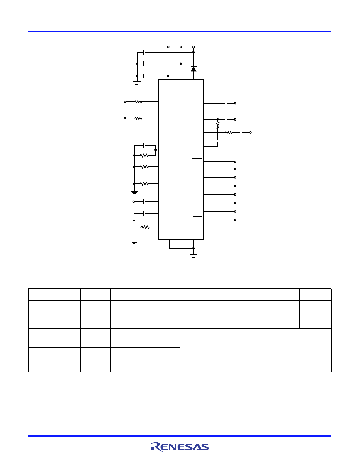
FIGURE 16. ISL5585 BASIC APPLICATION CIRCUIT
TL
R
TL
R
IN
DC, CFB
, C
PS3
PS1
PS2
1
0.5W,
matched to 0.1.
4.7F 20% 10V
0.1F 20% >100V
0.1F 20% 100V
1N400X type with breakdown > 100V.
Protection resistor values are application
dependent and will be determined by
protection requirements. Standard
applications will use 50 per side.
Basic Application Circuit Component List
COMPONENT VALUE TOLERANCE RATING COMPONENT VALUE TOLERANCE RATING
U1 - Ringing SLIC ISL5585 N/A N/A C
R
RT
R
SH
R
IL
R
S
R
TL
CIN, CRS, CTX, CRT,
C
POL
Design Parameters: Ring Trip Threshold = 90mA
I
SOURCE
and Ring terminals = 603.
= 100mA, I
20k 1% 0.1W C
49.9k 1% 0.1W C
71.5k 1% 0.1W D
66.5k 1% 0.1W RP1, RP2 = 50
17.8k 1% 0.1W
0.47F 20% 10V
= 120mA, Synthesize Device Impedance = 66.5K/133.3 = 500, with 51 protection resistors, impedance across Tip
SINK
. Switch Hook Threshold = 12mA, Loop Current Limit = 24.6mA, Transient current limit:
PEAK
AN1038 Rev 0.00 Page 11 of 14
Sep 2002
Page 12

AN1038 Rev 0.00 Page 12 of 14
Sep 2002
Evaluation Board Schematic
J5
J5
J5
J5
J5
J5
J5
J5
J5
J5
J6
J6
J6
J6
J6
J6
J6
J6
J6
J6
1
2
3
4
5
6
7
8
9
10
1
2
3
4
5
6
7
8
9
10
V
CC
+5V
+5V VBL VBH
CR3
JP3
CPS5
VREC
VXMIT
JP4
CODEC
CIN
CRS
1
3
5
2
4
6
CODEC
EXT
TRAP
JP7
THB
RTRAP
VRS
CTRAP
C1
CPS3
J5
TIP
J2
RING
J4
TIP
RING
J1
R14
+
-
CR4
CPS4
JP2
DTA
JP1
R15
RTA
1
28
5
6
25
27
26
CRT
RRT
RSH
RIL
+5V
+5V
CDC
+
CPOL
24
17
TIP
RING
SW+
SW-
TD
SH
ILIM
CDC
POL
AGND BGND
ALM
DET
BSEL
AUX
VRS
+5V
VBLVBH
ISL5585
VTX
-IN
VFB
SWC
E0
F0
F1
F2
NC
23 3 4
19
18
20
22
21
7
1
10
9
8
16
15
12
13
CTX
RS
RP CP
CFB
214
R1
CR1
R2
+5V
ALM
CR2
DET
BSEL
2
2
2
2
2
2
3
3
3
3
3
3
1
1
1
1
1
1
S6
S1
S2
S3
S4
S5
F2 F1
F2
E0 SWCF0
15 1 10
11
14
5
4
P
L
CP
U
/D
CE
P0 P1 P2 P3
Q1
Q2
Q3
TC
RC
GND = 8, V
CC
= 16
V
CC
3
2
6
7
12
13
FS_CNT
CE
U/D
CP
PL
P0 P1 P2 P3
Q0
Q1
Q2
Q3
TC
RC
V
CC
4
5
14
11
15 1 10 9
3
2
6
7
12
13
U2
74HC191M
GND = 8, VCC = 16
2.048MHz
512kHz
256kHz
JP10
1
3
5
2
4
6
V
CC
14
X0-43B
V
CC
U5
OUT
GND
8
7
C5 C6
JP12
MASTER
JP11
B2B
115
13
14
10
11
6
5
3
2
FS_IN
CLK_IN
DR_IN
110
111
210
211
310
311
410
411
SOE
4Y
3Y
2Y
1Y
CLK_OUT
FS_OUT
DT_OUT4
7
9
12
U4
74HC257M
R12
R13
VAG
R4
R3
R5
R6
R7
R8
15
JP9
PD
R11
R10
DR
DT
FS
J13
J12
J11
C2
0.1F6
CPS2
CPS1
1
3
5
7
9
11
13
15
17
19
ALM
DET
BSEL
F2
F1
F0
E0
SWC
R0+
R0-
P0-
P1
P0+
TC
TI-
VAC
TI+
V
DD
V
SS
0R
DT
FST
FSR
BCLKR
BCLKT
MCLK
_PCI
/A
1
2
3
4
5
17
18
19
20
JP8
A-LAW
U6
MC145484
8
13
7
14
9
12
11
16
10
9
Q0
2
4
6
8
10
12
14
16
18
20
V
CC
V
CC
V
CC
V
CC
J15
J8
J7
J10
CLK
C4
R9
1
3
5
7
9
11
13
15
17
19
DT_OUT
FS_OUT
CLK_OUT
2
4
6
8
10
12
14
16
18
20
J14
DR_IN
CLK_IN
FS_IN
DR_N
U2
74HC191M
TL
RTL
RIN
Page 13

ISL5585XEVAL1 Electrical Component List
COMPONENT VALUE TOLERANCE RATING COMPONENT VALUE TOLERANCE RATING
U
- Ringing SLIC HC5518x N/A N/A R3, R
1
U2, U
U
4
U
5
U
6
RRT, R
R
SH
R
IL
R
TA
R
S
R
P
R
, R
1
R
IN
3
TRAP
2
74HC191M N/A N/A R5, R6, R8, R9,
74HC257M N/A N/A R14, R15 51 5%, picked to
XO-43B N/A N/A CRT, CIN, CRS,
MC145484DW N/A N/A CDC, CFB 4.7F 20% 20V
20k 1% 0.10W CPS1, CPS2,
49.9k 1% 0.10W C2, C3, C4, C5, C6 0.1F 20% 20V
71.5k 1% 0.10W CR3 DL4003CT-ND N/A N/A
100 1% 0.25W DTA BAS21ZXCT N/A N/A
66.5k 1% 0.10W CR1, CR2 LN1251C N/A N/A
0 1% 0.10W R4 44.2k 1% 0.10W
499 1% 0.10W RTL 17.8k 1% 0.10W
66.5k 1% 0.10W
7
R10, R11, R12,
R13
CTX, C1, CPOL,
CTRAP
CPS3, CPS4,
CPS5
100k 1% 0.10W
10k 1% 0.10W
0.1
0.47F 20% 20V
0.1F 20% 100V
0.50W
ISL5585XEVAL1 Mechanical Component List
COMPONENT VALUE TOLERANCE RATING COMPONENT VALUE TOLERANCE RATING
U
- Socket 822271-1 N/A N/A J14, J15 10 Pin Header N/A N/A
1
U
Socket IC51-0202-347 N/A N/A J2, J3, J4 39F893 N/A N/A
6
J5, J6 43045-1000 N/A N/A JP5, JP10 3 Pin Header N/A N/A
J1 555165-1 N/A N/A JP1, JP2, JP3, JP4,
J7, J8, J9, J10, J11,
J12, J13
JP6, JP7, JP8, JP9,
JP11, JP12
CBJR20 N/A N/A S1, S2, S3, S4, S5,
S6
1 Pin Header
65F1681 N/A N/A
AN1038 Rev 0.00 Page 13 of 14
Sep 2002
Page 14

http://www.renesas.com
Refer to "http://www.renesas.com/" for the latest and detailed information.
Renesas Electronics America Inc.
1001 Murphy Ranch Road, Milpitas, CA 95035, U.S.A.
Tel: +1-408-432-8888, Fax: +1-408-434-5351
Renesas Electronics Canada Limited
9251 Yonge Street, Suite 8309 Richmond Hill, Ontario Canada L4C 9T3
Tel: +1-905-237-2004
Renesas Electronics Europe Limited
Dukes Meadow, Millboard Road, Bourne End, Buckinghamshire, SL8 5FH, U.K
Tel: +44-1628-651-700, Fax: +44-1628-651-804
Renesas Electronics Europe GmbH
Arcadiastrasse 10, 40472 Düsseldorf, Germany
Tel: +49-211-6503-0, Fax: +49-211-6503-1327
Renesas Electronics (China) Co., Ltd.
Room 1709 Quantum Plaza, No.27 ZhichunLu, Haidian District, Beijing, 100191 P. R. China
Tel: +86-10-8235-1155, Fax: +86-10-8235-7679
Renesas Electronics (Shanghai) Co., Ltd.
Unit 301, Tower A, Central Towers, 555 Langao Road, Putuo District, Shanghai, 200333 P. R. China
Tel: +86-21-2226-0888, Fax: +86-21-2226-0999
Renesas Electronics Hong Kong Limited
Unit 1601-1611, 16/F., Tower 2, Grand Century Place, 193 Prince Edward Road West, Mongkok, Kowloon, Hong Kong
Tel: +852-2265-6688, Fax: +852 2886-9022
Renesas Electronics Taiwan Co., Ltd.
13F, No. 363, Fu Shing North Road, Taipei 10543, Taiwan
Tel: +886-2-8175-9600, Fax: +886 2-8175-9670
Renesas Electronics Singapore Pte. Ltd.
80 Bendemeer Road, Unit #06-02 Hyflux Innovation Centre, Singapore 339949
Tel: +65-6213-0200, Fax: +65-6213-0300
Renesas Electronics Malaysia Sdn.Bhd.
Unit 1207, Block B, Menara Amcorp, Amcorp Trade Centre, No. 18, Jln Persiaran Barat, 46050 Petaling Jaya, Selangor Darul Ehsan, Malaysia
Tel: +60-3-7955-9390, Fax: +60-3-7955-9510
Renesas Electronics India Pvt. Ltd.
No.777C, 100 Feet Road, HAL 2nd Stage, Indiranagar, Bangalore 560 038, India
Tel: +91-80-67208700, Fax: +91-80-67208777
Renesas Electronics Korea Co., Ltd.
17F, KAMCO Yangjae Tower, 262, Gangnam-daero, Gangnam-gu, Seoul, 06265 Korea
Tel: +82-2-558-3737, Fax: +82-2-558-5338
SALES OFFICES
© 2018 Renesas Electronics Corporation. All rights reserved.
Colophon 7.0
(Rev.4.0-1 November 2017)
Notice
1. Descriptions of circuits, software and other related information in this document are provided only to illustrate the operation of semiconductor products and application examples. You are fully responsible for
the incorporation or any other use of the circuits, software, and information in the design of your product or system. Renesas Electronics disclaims any and all liability for any losses and damages incurred by
you or third parties arising from the use of these circuits, software, or information.
2. Renesas Electronics hereby expressly disclaims any warranties against and liability for infringement or any other claims involving patents, copyrights, or other intellectual property rights of third parties, by or
arising from the use of Renesas Electronics products or technical information described in this document, including but not limited to, the product data, drawings, charts, programs, algorithms, and application
examples.
3. No license, express, implied or otherwise, is granted hereby under any patents, copyrights or other intellectual property rights of Renesas Electronics or others.
4. You shall not alter, modify, copy, or reverse engineer any Renesas Electronics product, whether in whole or in part. Renesas Electronics disclaims any and all liability for any losses or damages incurred by
you or third parties arising from such alteration, modification, copying or reverse engineering.
5. Renesas Electronics products are classified according to the following two quality grades: “Standard” and “High Quality”. The intended applications for each Renesas Electronics product depends on the
product’s quality grade, as indicated below.
"Standard": Computers; office equipment; communications equipment; test and measurement equipment; audio and visual equipment; home electronic appliances; machine tools; personal electronic
equipment; industrial robots; etc.
"High Quality": Transportation equipment (automobiles, trains, ships, etc.); traffic control (traffic lights); large-scale communication equipment; key financial terminal systems; safety control equipment; etc.
Unless expressly designated as a high reliability product or a product for harsh environments in a Renesas Electronics data sheet or other Renesas Electronics document, Renesas Electronics products are
not intended or authorized for use in products or systems that may pose a direct threat to human life or bodily injury (artificial life support devices or systems; surgical implantations; etc.), or may cause
serious property damage (space system; undersea repeaters; nuclear power control systems; aircraft control systems; key plant systems; military equipment; etc.). Renesas Electronics disclaims any and all
liability for any damages or losses incurred by you or any third parties arising from the use of any Renesas Electronics product that is inconsistent with any Renesas Electronics data sheet, user’s manual or
other Renesas Electronics document.
6. When using Renesas Electronics products, refer to the latest product information (data sheets, user’s manuals, application notes, “General Notes for Handling and Using Semiconductor Devices” in the
reliability handbook, etc.), and ensure that usage conditions are within the ranges specified by Renesas Electronics with respect to maximum ratings, operating power supply voltage range, heat dissipation
characteristics, installation, etc. Renesas Electronics disclaims any and all liability for any malfunctions, failure or accident arising out of the use of Renesas Electronics products outside of such specified
ranges.
7. Although Renesas Electronics endeavors to improve the quality and reliability of Renesas Electronics products, semiconductor products have specific characteristics, such as the occurrence of failure at a
certain rate and malfunctions under certain use conditions. Unless designated as a high reliability product or a product for harsh environments in a Renesas Electronics data sheet or other Renesas
Electronics document, Renesas Electronics products are not subject to radiation resistance design. You are responsible for implementing safety measures to guard against the possibility of bodily injury, injury
or damage caused by fire, and/or danger to the public in the event of a failure or malfunction of Renesas Electronics products, such as safety design for hardware and software, including but not limited to
redundancy, fire control and malfunction prevention, appropriate treatment for aging degradation or any other appropriate measures. Because the evaluation of microcomputer software alone is very difficult
and impractical, you are responsible for evaluating the safety of the final products or systems manufactured by you.
8. Please contact a Renesas Electronics sales office for details as to environmental matters such as the environmental compatibility of each Renesas Electronics product. You are responsible for carefully and
sufficiently investigating applicable laws and regulations that regulate the inclusion or use of controlled substances, including without limitation, the EU RoHS Directive, and using Renesas Electronics
products in compliance with all these applicable laws and regulations. Renesas Electronics disclaims any and all liability for damages or losses occurring as a result of your noncompliance with applicable
laws and regulations.
9. Renesas Electronics products and technologies shall not be used for or incorporated into any products or systems whose manufacture, use, or sale is prohibited under any applicable domestic or foreign laws
or regulations. You shall comply with any applicable export control laws and regulations promulgated and administered by the governments of any countries asserting jurisdiction over the parties or
transactions.
10. It is the responsibility of the buyer or distributor of Renesas Electronics products, or any other party who distributes, disposes of, or otherwise sells or transfers the product to a third party, to notify such third
party in advance of the contents and conditions set forth in this document.
11. This document shall not be reprinted, reproduced or duplicated in any form, in whole or in part, without prior written consent of Renesas Electronics.
12. Please contact a Renesas Electronics sales office if you have any questions regarding the information contained in this document or Renesas Electronics products.
(Note 1) “Renesas Electronics” as used in this document means Renesas Electronics Corporation and also includes its directly or indirectly controlled subsidiaries.
(Note 2) “Renesas Electronics product(s)” means any product developed or manufactured by or for Renesas Electronics.
 Loading...