

Page 1
r
r
r
HSG2005
SiGe HBT
High Frequency Medium Power Amplifier
Features
• High Transition Frequency
f
= 28.5 GHz typ.
T
• Low Distortion and Excellent Linearity
P1dB at output = +21 dBm typ. f = 5.8 GHz
• High Collector to Emitter Voltage
V
= 5 V
CEO
• Ideal for 2 GHz, 5 GHz Band applications. e.g. WLAN, Digital cordless phone.
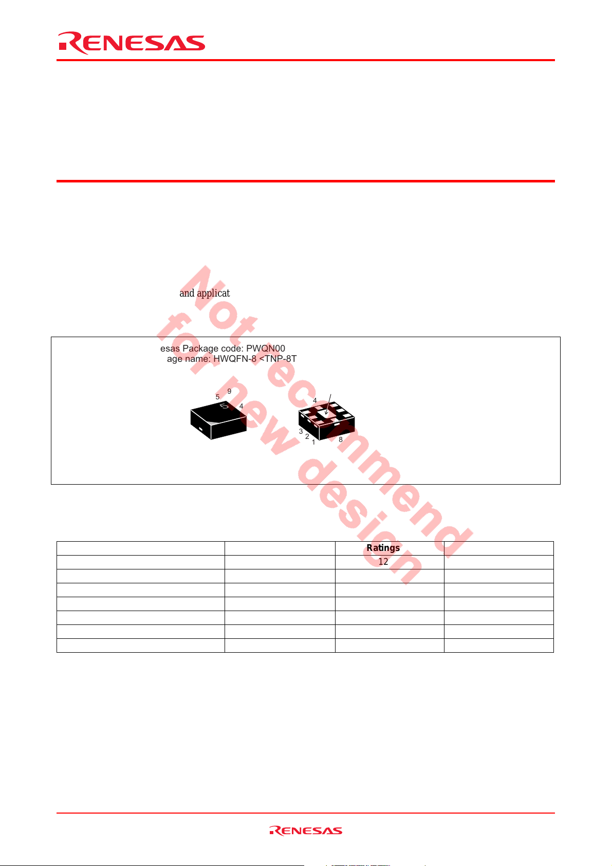
Outline
Renesas Package code: PWQN0008ZA-A
(Package name: HWQFN-8 <TNP-8TV>)
9
4
5
6
7
3
2
8
1
Note: Marking is “2005”.
7
8
6
2005
9
5
4
3
2
1
1. Collecto
2. Collecto
3. Collecto
4. Emitter
5. Emitter
6. Base
7. Emitter
8. Emitter
9. Emitter
REJ03G0485-0400
Rev.4.00
Jun 21, 2006
Absolute Maximum Ratings
(Ta = 25°C)
Item Symbol Ratings Unit
Collector to base voltage V
Collector to emitter voltage V
Emitter to base voltage V
Collector current IC 400 mA
Collector power dissipation Pc 1.2
Junction temperature Tj 150 °C
Storage temperature Tstg –55 to +150 °C
Note: Value on PCB (40 x 40 x 1.0 mm)
12 V
CBO
5 V
CEO
1.2 V
EBO
Note
W
Rev.4.00 Jun 21, 2006 page 1 of 12
Page 2
HSG2005
0
Electrical Characteristics
(Ta = 25°C)
Item Symbol Min Typ Max Unit Test Conditions
DC current transfer ratio hFE 150 220 300 VCE = 3 V, IC = 100 mA
Reverse Transfer Capacitance Cre 0.4 pF
Transition Frequency fT 28.5 GHz
Maximum Stable Gain MSG 10.5 12.5 dB
Maximum Available Gain MAG 17.0 dB
Maximum Available Gain MAG 9.0 dB
Power Gain PG 8.0 dB
1dB Compression Point at output
P1dB +21 dBm
Saturation Output Power Po(sat) +23 dBm
VCB = 3 V, IE = 0, f = 1 MHz,
emitter grounded
VCE = 3 V, IC = 100 mA,
f = 1 GHz
VCE = 3 V, IC = 100 mA,
f = 5.8 GHz
VCE = 3 V, IC = 100 mA,
f = 2.4 GHz
VCE = 3 V, IC = 100 mA,
f = 5.8 GHz
VCE = 3.6 V, I
= 100 mA,
idle
f = 5.8 GHz, Pin = +13 dBm
= 3.6 V, I
V
CE
= 100 mA,
idle
f = 5.8 GHz
VCE = 3.6 V, I
= 100 mA,
idle
f = 5.8 GHz, Pin = +13 dBm
Main Characteristics
Collector Power Dissipation Curve
1800
(mW)
*
1200
600
Collector Power Dissipation Pc
0 50 100 150 20
*(4 x 4 x 1mm) on PCB
Ambient Temperature Ta (°C)
Rev.4.00 Jun 21, 2006 page 2 of 12
Page 3
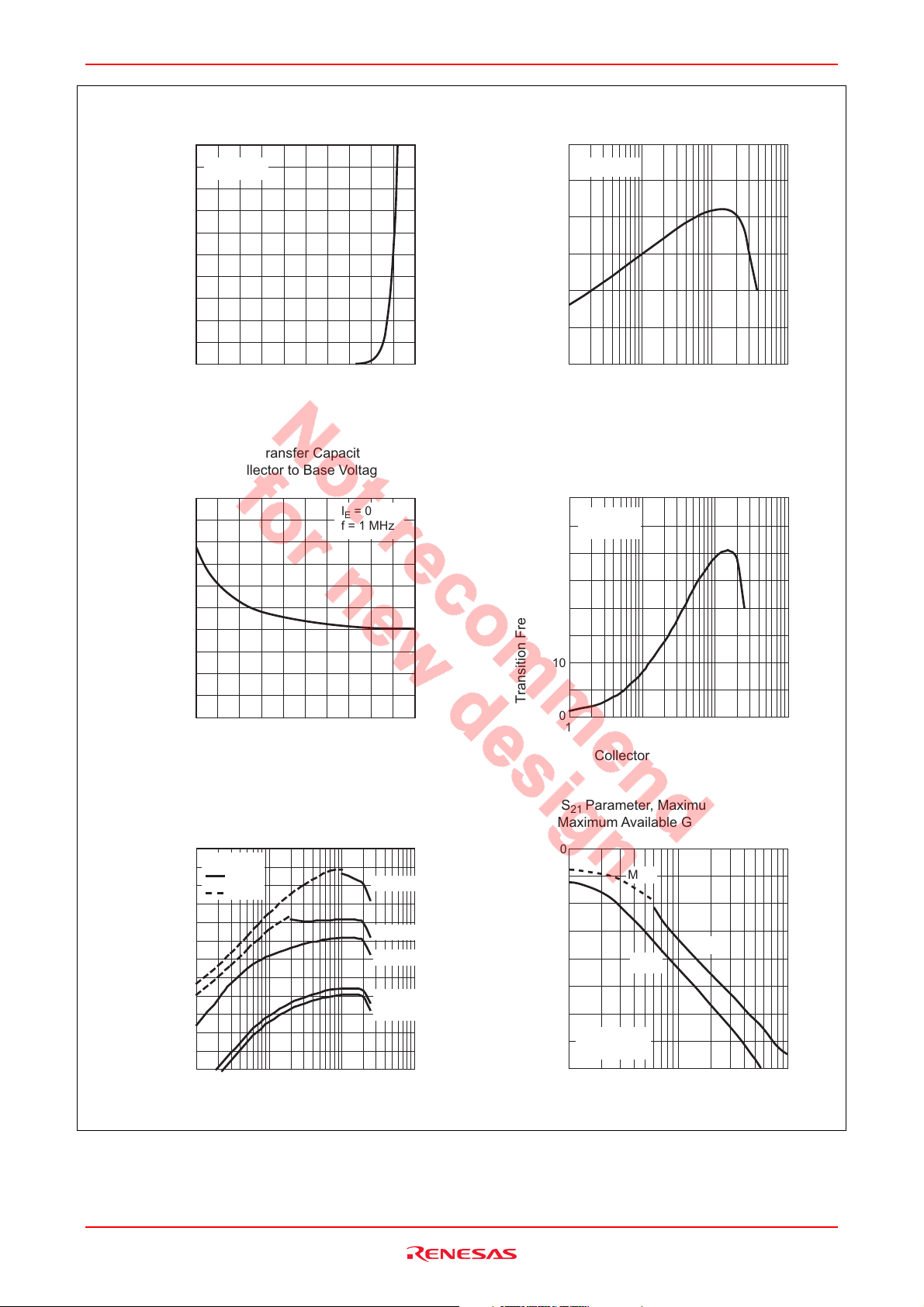
HSG2005
100
(mA)
C
Typical Transfer Characteristics
VCE = 3 V
80
60
(-)
FE
DC Current Transfer Ratio vs.
Collector Current
300
VCE = 3 V
200
40
20
Collector Current I
0 0.2 0.4 0.6 0.8 1.0
Base to Emitter Voltage VBE (V)
Reverse Transfer Capacitanse vs.
Collector to Base Voltage
1.0
(pF)
re
0.8
0.6
0.4
0.2
0.0
0123
Reverse Transfer Capacitanse C
I
f = 1 MHz
Collector to Base Voltage VCB (V)
100
DC Current Transfer Ratio h
0
1 10 1000
100
Collector Current IC (mA)
Transition Frequency vs.
Collector Current
= 0
E
40
(GHz)
30
T
20
10
VCE = 3 V
f = 1 GHz
Transition Frequency f
0
4
5
1 10 100 1000
Collector Current IC (mA)
Maximum Stable Gain, Maximum Available Gain
vs. Collector Current
30
VCE = 3 V
MAG
25
MSG
20
15
10
5
Maximum Stable Gain MSG (dB)
0
Maximum Available Gain MAG (dB)
1 10 100 1000
Collector Current I
Rev.4.00 Jun 21, 2006 page 3 of 12
C
f = 1 GHz
1.8 GHz
2.4 GHz
5.2 GHz
5.8 GHz
(mA)
S
Parameter, Maximum Stable Gain,
21
Maximum Available Gain vs. Frequency
40
MSG
(dB)
2
|
|S
Parameter
S
30
21
20
10
21
Maximum Stable Gain MSG (dB)
VCE = 3 V
I
= 100 mA
C
0
Maximum Available Gain MAG (dB)
0.1 1 10
|S21|
2
Frequency f (GHz)
MAG
Page 4
HSG2005
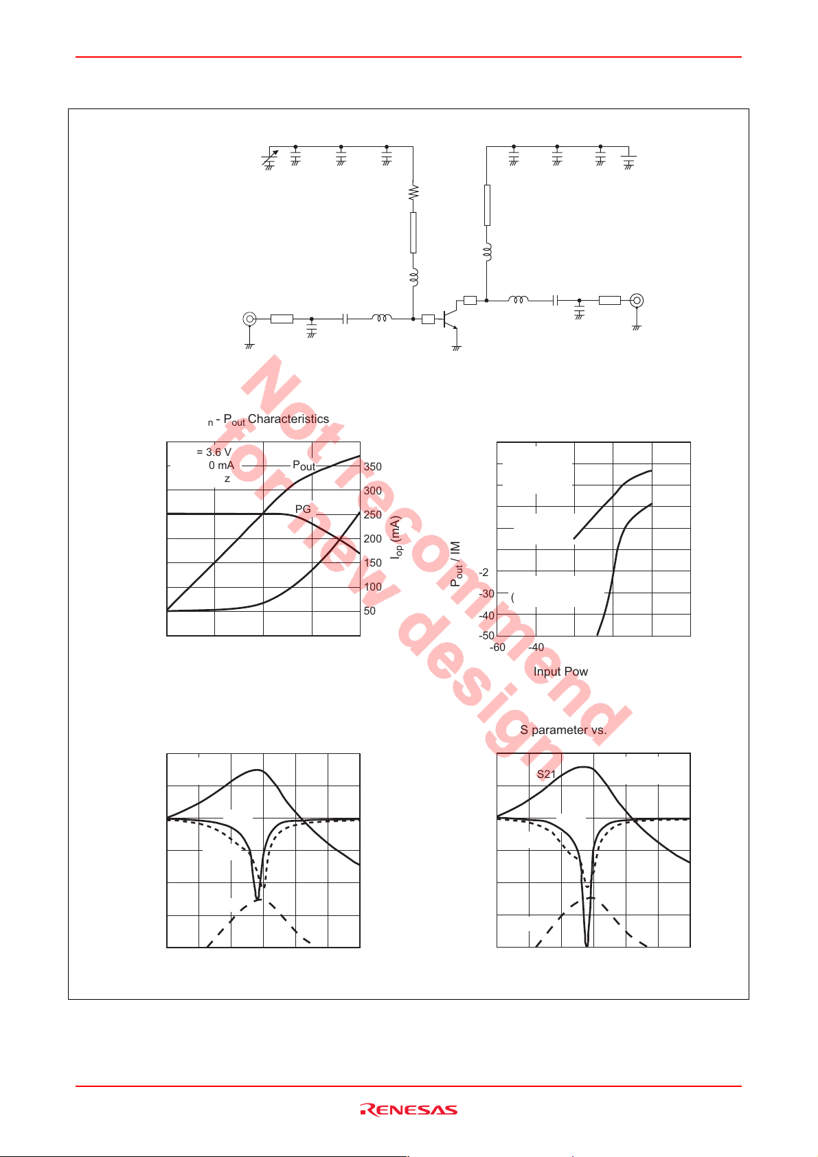
2.4 GHz Characteristics
Evaluation Board Circuit
VBB : Bias Control
IN
Pin - Pout Characteristics
P
- P
in
30
VCC = 3.6 V
I
25
20
= 50 mA
idle
f = 2.4 GHz
(dBm)
15
out
10
5
0
Power Gain PG (dB)
Output Power P
-5
-10
-20
-10
*1 µF
Characteristics
out
C : 1 to 2 pF
P
out
PG
I
op
10 200
1000 pF
C : 1 pF
10 pF
L : 5.6 nH
L : 1.5 nH
400
350
300
250
200
150
100
50
0
(mA)
op
I
27 Ω
VCC
10 pF
L : 10 nH
L : 1.8 nH
1000 pF
C : 1 pF
*1 µF
OUT
C : 0.9 pF
3rd. Order Intermodulation Distortion (IMD3)
40
VCE = 3.6 V
30
I
= 50 mA
idle
f = 2.4 GHz
20
10
Fundamental
0
-10
/ IMD3 (dBm)
-20
out
P
-30
-40
-50
(1tone)
IMD3
(2tone: ∆f = 1MHz)
-40 0 40-20-60
20
Input Power P
S parameter vs. Frequency
20
VCE = 3.6 V
I
= 50 mA
C
10
0
-10
-20
S parameter (dB)
-30
-40
S22
1.5 3.0 4.02.51.0
(dBm)
in
S21
S11
S12
2.0 3.5
Frequency f (GHz)
Input Power Pin (dBm)
S parameter vs. Frequency
20
10
0
-10
-20
S21
S22
S parameter (dB)
-30
-40
S12
1.0
1.5 3.0 4.02.5
VCE = 3.6 V
I
C
S11
2.0 3.5
Frequency f (GHz)
= 150 mA
Rev.4.00 Jun 21, 2006 page 4 of 12
Page 5

HSG2005
5.8 GHz Characteristics
Evaluation Board Circuit
VBB : Bias Control
Pin - Pout Characteristics
P
- P
in
25
VCC = 3.6 V
I
= 100 mA
idle
20
f = 5.8 GHz
(dBm)
out
15
10
Power Gain PG (dB)
Output Power P
5
0
0
5
*1 µF
IN
Characteristics
out
P
out
1000 pF
0.5 pF
I
PG
15 2010
op
2 pF
10 pF
0.2 pF
250
200
150
100
50
0
27 Ω
(mA)
op
I
VCC
10 pF
0.5 pF
1000 pF
2 pF
0.4 pF
*1 µF
OUT
3rd. Order Intermodulation Distortion (IMD3)
40
VCE = 3.6 V
30
I
= 100 mA
idle
f = 5.8 GHz
20
10
Fundamental
0
-10
/ IMD3 (dBm)
-20
out
P
-30
-40
-50
(1tone)
IMD3
(2tone: ∆f = 1MHz)
-40 0 40-20-60
20
Input Power P
S parameter vs. Frequency
10
S21
0
-10
S parameter (dB)
-20
-30
S22
S12
57864
(dBm)
in
VCE = 3.6 V
I
C
S11
Frequency f (GHz)
= 100 mA
Input Power Pin (dBm)
S parameter vs. Frequency
10
S21
0
-10
S parameter (dB)
-20
-30
S22
S12
57864
VCE = 3.6 V
I
= 150 mA
C
S11
Frequency f (GHz)
Rev.4.00 Jun 21, 2006 page 5 of 12
Page 6

HSG2005
S
Parameter vs. Frequency
11
1
.4
.2
0
-.2
.2
-.4
Condition: V
.8
.6
.6
.4
.8
-.6
-.8
-1
= 3 V, IC = 100 mA, Zo = 50 Ω
CE
1.5
2
3
4
5
10
1.5
234
1
-1.5
10
5
-10
-5
-4
-3
-2
100 to 3000 MHz (100 MHz Step)
3200 to 6000 MHz (200 MHz Step)
Parameter vs. Frequency
S
21
Scale: 20 / div.
60°
-30°
-60°
150°
180°
-150°
Condition: V
90°
120°
-120°
CE
-90°
= 3 V, IC = 100 mA, Zo = 50 Ω
100 to 3000 MHz (100 MHz Step)
3200 to 6000 MHz (200 MHz Step)
30°
0°
Parameter vs. Frequency S22 Parameter vs. Frequency
S
150°
180°
-150°
Condition: V
12
120°
-120°
CE
-90°
= 3 V, IC = 100 mA, Zo = 50 Ω
90°
Scale: 0.04 / div.
60°
30°
-30°
-60°
100 to 3000 MHz (100 MHz Step)
3200 to 6000 MHz (200 MHz Step)
1
.8
.6
.4
.2
0°
0
-.2
.2
-.4
Condition: V
.6
.4
.8
-.6
-.8
-1
= 3 V, IC = 100 mA, Zo = 50 Ω
CE
1.5
2
3
4
5
10
1.5
234
1
-1.5
10
5
-10
-5
-4
-3
-2
100 to 3000 MHz (100 MHz Step)
3200 to 6000 MHz (200 MHz Step)
Rev.4.00 Jun 21, 2006 page 6 of 12
Page 7

HSG2005
Ω
Ω
S
Parameter vs. Frequency
11
1
.4
.2
0
-.2
.2
-.4
Condition: V
.8
.6
.6
.4
.8
-.6
-.8
-1
= 3.3 V, IC = 100 mA, Zo = 50 Ω
CE
1.5
2
3
4
5
10
1.5
234
1
-1.5
10
5
-10
-5
-4
-3
-2
100 to 3000 MHz (100 MHz Step)
3200 to 6000 MHz (200 MHz Step)
Parameter vs. Frequency
S
21
Scale: 20 / div.
60°
-30°
-60°
150°
180°
-150°
Condition: V
90°
120°
-120°
-90°
= 3.3 V, IC = 100 mA, Zo = 50
CE
100 to 3000 MHz (100 MHz Step)
3200 to 6000 MHz (200 MHz Step)
30°
0°
Parameter vs. Frequency S22 Parameter vs. Frequency
S
150°
180°
-150°
Condition: V
12
120°
-120°
CE
-90°
= 3.3 V, IC = 100 mA, Zo = 50 Ω
Scale: 0.04 / div.
90°
60°
30°
-30°
-60°
100 to 3000 MHz (100 MHz Step)
3200 to 6000 MHz (200 MHz Step)
1
.8
.6
.4
.2
0°
0
-.2
.2
-.4
Condition: V
.6
.4
.8
-.6
-.8
-1
= 3.3 V, IC = 100 mA, Zo = 50
CE
1.5
2
3
4
5
10
1.5
234
1
-1.5
10
5
-10
-5
-4
-3
-2
100 to 3000 MHz (100 MHz Step)
3200 to 6000 MHz (200 MHz Step)
Rev.4.00 Jun 21, 2006 page 7 of 12
Page 8

HSG2005
Ω
Ω
S
Parameter vs. Frequency
11
1
.4
.2
0
-.2
.2
-.4
Condition: V
.8
.6
.6
.4
.8
-.6
-.8
-1
= 3.6 V, IC = 100 mA, Zo = 50 Ω
CE
1.5
2
3
4
5
10
1.5
234
1
-1.5
10
5
-10
-5
-4
-3
-2
100 to 3000 MHz (100 MHz Step)
3200 to 6000 MHz (200 MHz Step)
Parameter vs. Frequency
S
21
Scale: 20 / div.
60°
-30°
-60°
150°
180°
-150°
Condition: V
90°
120°
-120°
-90°
= 3.6 V, IC = 100 mA, Zo = 50
CE
100 to 3000 MHz (100 MHz Step)
3200 to 6000 MHz (200 MHz Step)
30°
0°
Parameter vs. Frequency S22 Parameter vs. Frequency
S
150°
180°
-150°
Condition: V
12
120°
-120°
CE
-90°
= 3.6 V, IC = 100 mA, Zo = 50 Ω
Scale: 0.04 / div.
90°
60°
30°
-30°
-60°
100 to 3000 MHz (100 MHz Step)
3200 to 6000 MHz (200 MHz Step)
1
.8
.6
.4
.2
0°
0
-.2
.2
-.4
Condition: V
.6
.4
.8
-.6
-.8
-1
= 3.6 V, IC = 100 mA, Zo = 50
CE
1.5
2
3
4
5
10
1.5
234
1
-1.5
10
5
-10
-5
-4
-3
-2
100 to 3000 MHz (100 MHz Step)
3200 to 6000 MHz (200 MHz Step)
Rev.4.00 Jun 21, 2006 page 8 of 12
Page 9

HSG2005
S parameter
(VCE = 3 V, IC = 100 mA, Zo = 50 Ω)
f (MHz)
100 0.687 -139.8 77.53 120.52 0.0084 45.8 0.682 -105.5
200 0.775 -160.8 47.14 104.05 0.0106 28.1 0.598 -134.6
300 0.786 -169.2 32.99 96.02 0.0107 33.1 0.566 -148.2
400 0.792 -174.5 24.95 91.32 0.0127 39.8 0.559 -155.7
500 0.797 -178.1 19.96 87.93 0.0129 39.0 0.559 -160.4
600 0.802 179.0 16.62 85.12 0.0139 41.5 0.560 -163.5
700 0.803 176.6 14.22 82.63 0.0155 42.8 0.560 -165.9
800 0.804 174.2 12.41 80.38 0.0163 48.0 0.561 -167.7
900 0.802 171.9 10.98 78.31 0.0176 49.1 0.563 -169.1
1000 0.804 169.8 9.81 76.55 0.0191 50.1 0.565 -170.4
1100 0.807 168.1 8.89 74.86 0.0201 51.0 0.567 -171.4
1200 0.809 166.5 8.11 73.18 0.0214 51.7 0.568 -172.3
1300 0.809 164.8 7.47 71.47 0.0230 52.7 0.570 -173.0
1400 0.809 163.1 6.91 69.76 0.0244 53.8 0.572 -173.8
1500 0.809 161.2 6.43 68.18 0.0257 53.0 0.573 -174.5
1600 0.811 159.5 6.00 66.70 0.0275 54.4 0.576 -175.1
1700 0.814 158.1 5.62 65.37 0.0280 54.6 0.578 -175.6
1800 0.817 156.9 5.29 63.93 0.0295 54.2 0.579 -176.0
1900 0.817 155.6 5.00 62.42 0.0314 54.2 0.581 -176.4
2000 0.816 154.0 4.74 60.74 0.0324 54.5 0.583 -176.9
2100 0.814 152.3 4.49 59.29 0.0335 54.4 0.584 -177.3
2200 0.817 150.8 4.28 57.89 0.0350 53.9 0.586 -177.7
2300 0.820 149.5 4.08 56.76 0.0364 53.1 0.587 -178.0
2400 0.824 148.4 3.90 55.44 0.0381 53.8 0.590 -178.4
2500 0.825 147.3 3.73 54.01 0.0389 53.4 0.591 -178.7
2600 0.823 145.8 3.58 52.41 0.0405 52.5 0.591 -179.0
2700 0.822 144.3 3.44 50.91 0.0416 52.6 0.593 -179.4
2800 0.822 142.8 3.30 49.54 0.0432 52.5 0.594 -179.8
2900 0.824 141.5 3.18 48.34 0.0440 51.5 0.595 179.9
3000 0.827 140.4 3.07 47.15 0.0458 51.0 0.596 179.5
3200 0.828 137.9 2.87 44.27 0.0481 50.3 0.596 178.8
3400 0.824 134.8 2.68 41.22 0.0509 49.1 0.596 178.0
3600 0.826 132.4 2.53 38.75 0.0539 48.0 0.597 177.0
3800 0.827 129.6 2.39 35.90 0.0562 46.1 0.597 175.8
4000 0.826 126.2 2.25 32.65 0.0587 44.6 0.597 174.5
4200 0.830 123.6 2.13 29.93 0.0608 43.6 0.596 173.0
4400 0.830 120.8 2.03 27.16 0.0632 41.6 0.596 171.3
4600 0.832 117.3 1.92 23.82 0.0656 40.2 0.597 169.4
4800 0.839 114.6 1.82 20.87 0.0675 38.3 0.599 167.4
5000 0.841 111.9 1.74 18.04 0.0699 36.1 0.601 165.3
5200 0.843 108.6 1.65 14.81 0.0719 34.1 0.606 163.1
5400 0.851 106.1 1.56 11.85 0.0734 32.2 0.612 160.9
5600 0.854 103.6 1.49 8.83 0.0750 29.8 0.618 158.5
5800 0.856 100.5 1.41 5.79 0.0763 27.5 0.624 156.3
6000 0.862 98.4 1.34 2.79 0.0776 25.4 0.631 153.9
MAG ANG (deg.) MAG ANG (deg.) MAG ANG (deg.) MAG ANG (deg.)
S11 S21 S12 S22
Rev.4.00 Jun 21, 2006 page 9 of 12
Page 10

HSG2005
S parameter
(VCE = 3.3 V, IC = 100 mA, Zo = 50 Ω)
f (MHz)
100 0.675 -140.9 80.79 120.97 0.0127 40.9 0.626 -109.1
200 0.771 -160.6 48.16 104.58 0.0091 37.0 0.594 -134.0
300 0.785 -168.9 33.50 96.32 0.0110 34.4 0.561 -147.6
400 0.790 -174.3 25.29 91.50 0.0128 37.4 0.554 -155.1
500 0.794 -178.0 20.21 88.06 0.0135 41.0 0.553 -159.7
600 0.800 179.2 16.83 85.22 0.0140 42.0 0.553 -163.0
700 0.802 176.7 14.40 82.70 0.0157 44.5 0.554 -165.4
800 0.802 174.3 12.56 80.43 0.0169 47.1 0.555 -167.2
900 0.801 172.0 11.11 78.33 0.0177 49.5 0.557 -168.8
1000 0.802 170.0 9.93 76.55 0.0191 52.1 0.559 -170.0
1100 0.805 168.2 8.99 74.86 0.0204 50.3 0.561 -171.0
1200 0.808 166.6 8.20 73.16 0.0211 51.6 0.563 -171.9
1300 0.808 164.9 7.56 71.44 0.0228 52.5 0.564 -172.7
1400 0.808 163.1 6.99 69.73 0.0247 53.4 0.566 -173.4
1500 0.807 161.3 6.51 68.13 0.0252 53.4 0.567 -174.0
1600 0.809 159.6 6.07 66.63 0.0268 53.9 0.570 -174.7
1700 0.813 158.3 5.68 65.30 0.0281 53.8 0.572 -175.2
1800 0.816 157.0 5.35 63.86 0.0294 54.0 0.574 -175.7
1900 0.816 155.7 5.05 62.34 0.0309 53.8 0.575 -176.1
2000 0.814 154.1 4.79 60.66 0.0323 54.4 0.578 -176.5
2100 0.813 152.4 4.55 59.20 0.0335 54.6 0.579 -176.9
2200 0.816 150.9 4.33 57.79 0.0348 54.0 0.581 -177.3
2300 0.819 149.6 4.12 56.67 0.0362 53.4 0.582 -177.7
2400 0.823 148.5 3.94 55.32 0.0378 53.2 0.584 -178.0
2500 0.824 147.3 3.77 53.88 0.0391 52.9 0.586 -178.3
2600 0.822 145.9 3.62 52.28 0.0409 53.1 0.586 -178.6
2700 0.820 144.3 3.47 50.76 0.0422 52.6 0.588 -179.0
2800 0.821 142.9 3.34 49.39 0.0423 52.1 0.589 -179.4
2900 0.823 141.6 3.22 48.20 0.0444 51.8 0.590 -179.7
3000 0.826 140.5 3.11 47.01 0.0457 51.4 0.591 180.0
3200 0.827 137.9 2.90 44.10 0.0480 50.6 0.592 179.3
3400 0.823 134.9 2.71 41.04 0.0512 49.0 0.592 178.4
3600 0.826 132.4 2.55 38.57 0.0533 47.8 0.593 177.4
3800 0.826 129.6 2.41 35.71 0.0558 46.9 0.592 176.3
4000 0.826 126.3 2.28 32.44 0.0588 45.3 0.593 175.0
4200 0.830 123.7 2.16 29.71 0.0609 43.6 0.592 173.4
4400 0.829 120.8 2.05 26.93 0.0629 41.7 0.592 171.8
4600 0.831 117.3 1.94 23.60 0.0648 40.0 0.593 169.8
4800 0.838 114.7 1.84 20.64 0.0674 38.3 0.595 167.8
5000 0.841 112.0 1.76 17.79 0.0696 36.7 0.598 165.8
5200 0.842 108.7 1.66 14.56 0.0719 34.5 0.603 163.5
5400 0.850 106.1 1.58 11.59 0.0731 32.2 0.608 161.3
5600 0.855 103.6 1.51 8.56 0.0746 29.9 0.615 159.0
5800 0.856 100.5 1.43 5.51 0.0762 27.7 0.621 156.7
6000 0.862 98.4 1.35 2.51 0.0770 25.6 0.629 154.3
MAG ANG (deg.) MAG ANG (deg.) MAG ANG (deg.) MAG ANG (deg.)
S11 S21 S12 S22
Rev.4.00 Jun 21, 2006 page 10 of 12
Page 11

HSG2005
S parameter
(VCE = 3.6 V, IC = 100 mA, Zo = 50 Ω)
f (MHz)
100 0.669 -141.0 82.98 121.53 0.0107 60.0 0.695 -107.8
200 0.763 -160.3 48.82 105.15 0.0118 37.6 0.583 -133.1
300 0.781 -168.8 33.85 96.65 0.0104 31.8 0.556 -146.8
400 0.787 -174.2 25.53 91.73 0.0110 37.4 0.550 -154.7
500 0.793 -177.9 20.40 88.22 0.0131 38.2 0.548 -159.3
600 0.799 179.3 16.98 85.36 0.0145 43.2 0.548 -162.5
700 0.800 176.8 14.52 82.79 0.0157 44.8 0.549 -165.0
800 0.801 174.4 12.67 80.50 0.0165 46.4 0.550 -166.9
900 0.800 172.1 11.21 78.40 0.0172 47.4 0.552 -168.4
1000 0.801 170.0 10.02 76.59 0.0190 49.6 0.553 -169.7
1100 0.804 168.3 9.07 74.88 0.0203 48.8 0.556 -170.7
1200 0.807 166.7 8.27 73.18 0.0216 52.1 0.558 -171.6
1300 0.807 165.0 7.62 71.44 0.0228 53.0 0.560 -172.3
1400 0.806 163.2 7.06 69.72 0.0242 53.8 0.561 -173.1
1500 0.806 161.3 6.56 68.12 0.0255 53.7 0.563 -173.7
1600 0.809 159.7 6.12 66.61 0.0268 54.4 0.565 -174.3
1700 0.812 158.3 5.73 65.26 0.0282 54.9 0.567 -174.9
1800 0.814 157.1 5.39 63.81 0.0297 54.0 0.569 -175.3
1900 0.815 155.7 5.10 62.28 0.0311 54.1 0.571 -175.7
2000 0.813 154.1 4.83 60.60 0.0324 54.4 0.573 -176.1
2100 0.812 152.5 4.58 59.13 0.0335 54.2 0.575 -176.6
2200 0.814 150.9 4.36 57.72 0.0348 54.2 0.577 -177.0
2300 0.818 149.7 4.16 56.58 0.0365 53.4 0.578 -177.3
2400 0.822 148.5 3.98 55.23 0.0381 53.5 0.580 -177.6
2500 0.822 147.3 3.81 53.78 0.0389 53.4 0.581 -178.0
2600 0.821 145.9 3.65 52.18 0.0402 53.0 0.583 -178.3
2700 0.820 144.4 3.50 50.66 0.0416 53.2 0.584 -178.7
2800 0.819 142.9 3.37 49.28 0.0429 51.7 0.585 -179.0
2900 0.822 141.6 3.24 48.08 0.0443 51.9 0.586 -179.3
3000 0.825 140.5 3.13 46.89 0.0453 51.2 0.587 -179.7
3200 0.826 137.9 2.92 43.98 0.0482 50.0 0.588 179.6
3400 0.823 134.9 2.73 40.91 0.0505 49.5 0.589 178.7
3600 0.825 132.5 2.57 38.42 0.0533 48.0 0.589 177.8
3800 0.825 129.7 2.43 35.54 0.0559 46.2 0.589 176.6
4000 0.825 126.3 2.29 32.27 0.0582 45.6 0.589 175.3
4200 0.829 123.7 2.17 29.53 0.0603 43.9 0.589 173.8
4400 0.828 120.9 2.06 26.75 0.0627 41.8 0.589 172.1
4600 0.830 117.4 1.95 23.41 0.0653 40.4 0.590 170.2
4800 0.838 114.7 1.85 20.45 0.0671 38.2 0.592 168.2
5000 0.840 112.0 1.77 17.60 0.0694 36.3 0.595 166.1
5200 0.842 108.7 1.68 14.35 0.0712 34.3 0.599 163.9
5400 0.850 106.1 1.59 11.39 0.0730 32.3 0.606 161.6
5600 0.854 103.6 1.52 8.34 0.0749 29.6 0.612 159.3
5800 0.856 100.5 1.44 5.27 0.0761 28.1 0.619 157.0
6000 0.861 98.4 1.36 2.29 0.0768 25.7 0.626 154.7
MAG ANG (deg.) MAG ANG (deg.) MAG ANG (deg.) MAG ANG (deg.)
S11 S21 S12 S22
Rev.4.00 Jun 21, 2006 page 11 of 12
Page 12

HSG2005
Package Dimensions
Package Name
HWQFN-8
P-HWQFN8-2x2-0.65 PWQN0008ZA-A TNP-8TV 0.009g
MASS[Typ.]RENESAS CodeJEITA Package Code Previous Code
B
76
E
8448
1
S
D
5
2
3
y
1
y
S
A
E
Z
Z
S
A
1
A
b
5
32
D
MxSA
6
0.90
C0.15
e
B
7
p
L
0.60
0.05
1
Dimension in Millimeters
Reference
Symbol
Min Nom Max
1.965
2.00
D
1.965
E
A
0
A
1
A
2
b
e
L
p
x
y
y
1
Z
D
Z
E
2.00
0.3
0.65
0.35
0.350
0.225
2.075
2.075
0.80
0.05
0.10
0.08
0.10
Ordering Information
Part Name Quantity Shipping Container
HSG2005TB-E 2000 pcs. φ178 mm Reel, 8 mm Emboss taping
Note: Therefore especially small contact area of terminal, miss contact may occur if inadequate soldering condition is
applied.
Contact Renesas sales office for any question regarding recommended soldering conditio n of Renesas.
Rev.4.00 Jun 21, 2006 page 12 of 12
Page 13

Sales Strategic Planning Div. Nippon Bldg., 2-6-2, Ohte-machi, Chiyoda-ku, Tokyo 100-0004, Japan
Keep safety first in your circuit designs!
1. Renesas Technology Corp. puts the maximum effort into making semiconductor products better and more reliable, but there is always the possibility that trouble
may occur with them. Trouble with semiconductors may lead to personal injury, fire or property damage.
Remember to give due consideration to safety when making your circuit designs, with appropriate measures such as (i) placement of substitutive, auxiliary
circuits, (ii) use of nonflammable material or (iii) prevention against any malfunction or mishap.
Notes regarding these materials
1. These materials are intended as a reference to assist our customers in the selection of the Renesas Technology Corp. product best suited to the customer's
application; they do not convey any license under any intellectual property rights, or any other rights, belonging to Renesas Technology Corp. or a third party.
2. Renesas Technology Corp. assumes no responsibility for any damage, or infringement of any third-party's rights, originating in the use of any product data,
diagrams, charts, programs, algorithms, or circuit application examples contained in these materials.
3. All information contained in these materials, including product data, diagrams, charts, programs and algorithms represents information on products at the time of
publication of these materials, and are subject to change by Renesas Technology Corp. without notice due to product improvements or other reasons. It is
therefore recommended that customers contact Renesas Technology Corp. or an authorized Renesas Technology Corp. product distributor for the latest product
information before purchasing a product listed herein.
The information described here may contain technical inaccuracies or typographical errors.
Renesas Technology Corp. assumes no responsibility for any damage, liability, or other loss rising from these inaccuracies or errors.
Please also pay attention to information published by Renesas Technology Corp. by various means, including the Renesas Technology Corp. Semiconductor
home page (http://www.renesas.com).
4. When using any or all of the information contained in these materials, including product data, diagrams, charts, programs, and algorithms, please be sure to
evaluate all information as a total system before making a final decision on the applicability of the information and products. Renesas Technology Corp. assumes
no responsibility for any damage, liability or other loss resulting from the information contained herein.
5. Renesas Technology Corp. semiconductors are not designed or manufactured for use in a device or system that is used under circumstances in which human life
is potentially at stake. Please contact Renesas Technology Corp. or an authorized Renesas Technology Corp. product distributor when considering the use of a
product contained herein for any specific purposes, such as apparatus or systems for transportation, vehicular, medical, aerospace, nuclear, or undersea repeater
use.
6. The prior written approval of Renesas Technology Corp. is necessary to reprint or reproduce in whole or in part these materials.
7. If these products or technologies are subject to the Japanese export control restrictions, they must be exported under a license from the Japanese government and
cannot be imported into a country other than the approved destination.
Any diversion or reexport contrary to the export control laws and regulations of Japan and/or the country of destination is prohibited.
8. Please contact Renesas Technology Corp. for further details on these materials or the products contained therein.
RENESAS SALES OFFICES
http://www.renesas.com
Refer to "http://www.renesas.com/en/network" for the latest and detailed information.
Renesas Technology America, Inc.
450 Holger Way, San Jose, CA 95134-1368, U.S.A
Tel: <1> (408) 382-7500, Fax: <1> (408) 382-7501
Renesas Technology Europe Limited
Dukes Meadow, Millboard Road, Bourne End, Buckinghamshire, SL8 5FH, U.K.
Tel: <44> (1628) 585-100, Fax: <44> (1628) 585-900
Renesas Technology (Shanghai) Co., Ltd.
Unit 204, 205, AZIACenter, No.1233 Lujiazui Ring Rd, Pudong District, Shanghai, China 200120
Tel: <86> (21) 5877-1818, Fax: <86> (21) 6887-7898
Renesas Technology Hong Kong Ltd.
7th Floor, North Tower, World Finance Centre, Harbour City, 1 Canton Road, Tsimshatsui, Kowloon, Hong Kong
Tel: <852> 2265-6688, Fax: <852> 2730-6071
Renesas Technology Taiwan Co., Ltd.
10th Floor, No.99, Fushing North Road, Taipei, Taiwan
Tel: <886> (2) 2715-2888, Fax: <886> (2) 2713-2999
Renesas Technology Singapore Pte. Ltd.
1 Harbour Front Avenue, #06-10, Keppel Bay Tower, Singapore 098632
Tel: <65> 6213-0200, Fax: <65> 6278-8001
Renesas Technology Korea Co., Ltd.
Kukje Center Bldg. 18th Fl., 191, 2-ka, Hangang-ro, Yongsan-ku, Seoul 140-702, Korea
Tel: <82> (2) 796-3115, Fax: <82> (2) 796-2145
Renesas Technology Malaysia Sdn. Bhd
Unit 906, Block B, Menara Amcorp, Amcorp Trade Centre, No.18, Jalan Persiaran Barat, 46050 Petaling Jaya, Selangor Darul Ehsan, Malaysia
Tel: <603> 7955-9390, Fax: <603> 7955-9510
© 2006. Renesas Technology Corp., All rights reserved. Printed in Japan.
Colophon .6.0
 Loading...