

Page 1
r
r
r
HSG2004
SiGe HBT
High Frequency Medium Power Amplifier
Features
• High Transition Frequency
f
= 30 GHz typ.
T
• Low Distortion and Excellent Linearity
P1dB at output = +14.5 dBm typ. f = 5.8 GHz
• High Collector to Emitter Voltage
V
= 5 V
CEO
• Ideal for 2 GHz, 5 GHz Band applications. e.g. WLAN, Digital cordless phone.
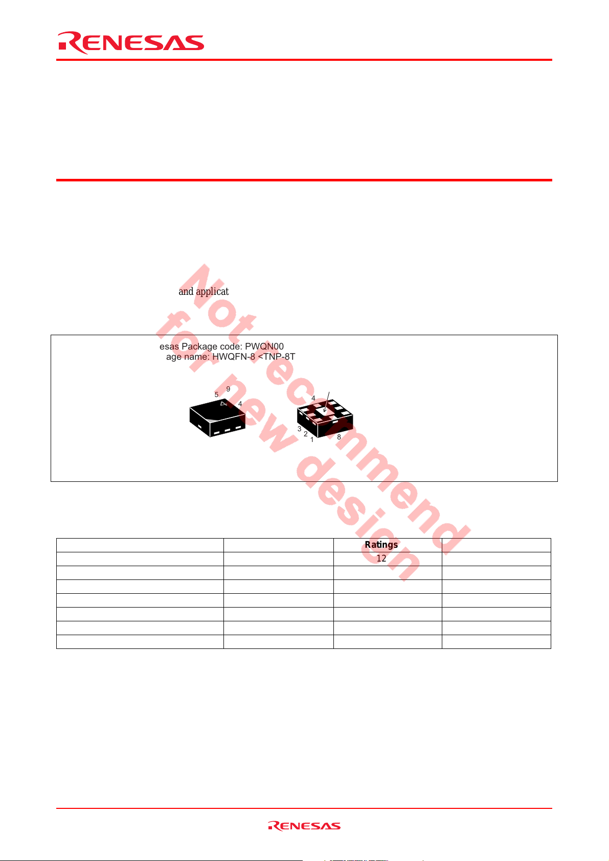
Outline
Renesas Package code: PWQN0008ZA-A
(Package name: HWQFN-8 <TNP-8TV>)
9
4
5
6
7
3
2
8
1
Note: Marking is “2004”.
7
8
6
2004
9
5
4
3
2
1
1. Collecto
2. Collecto
3. Collecto
4. Emitter
5. Emitter
6. Base
7. Emitter
8. Emitter
9. Emitter
REJ03G0484-0400
Rev.4.00
Jun 21, 2006
Absolute Maximum Ratings
(Ta = 25°C)
Item Symbol Ratings Unit
Collector to base voltage V
Collector to emitter voltage V
Emitter to base voltage V
Collector current IC 200 mA
Collector power dissipation Pc 1
Junction temperature Tj 150 °C
Storage temperature Tstg –55 to +150 °C
Note: Value on PCB (40 x 40 x 1.0 mm)
12 V
CBO
5 V
CEO
1.2 V
EBO
Note
W
Rev.4.00 Jun 21, 2006 page 1 of 12
Page 2
HSG2004
0
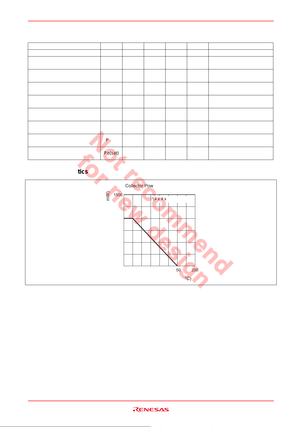
Electrical Characteristics
(Ta = 25°C)
Item Symbol Min Typ Max Unit Test Conditions
DC current transfer ratio hFE 170 240 320 VCE = 3 V, IC = 30 mA
Reverse Transfer Capacitance
0.6 pF
C
re
Transition Frequency fT 30.0 GHz
Maximum Stable Gain MSG 14 15.5 dB
Maximum Available Gain MAG 21 dB
Maximum Available Gain MAG 12 dB
Power Gain PG 11.5 dB
1dB Compression Point at output
P1dB +14.5 dBm
Saturation Output Power Po(sat) +22 dBm
VCB = 3 V, IE = 0, f = 1 MHz,
emitter grounded
VCE = 3 V, IC = 30 mA,
f = 1 GHz
VCE = 3 V, IC = 30 mA,
f = 5.8 GHz
VCE = 3 V, IC = 30 mA,
f = 2.4 GHz
VCE = 3 V, IC = 30 mA,
f = 5.8 GHz
VCE = 3.6 V, I
= 30 mA,
idle
f = 5.8 GHz, Pin = +0 dBm
= 3.6 V, I
V
CE
= 30 mA,
idle
f = 5.8 GHz
VCE = 3.6 V, I
= 30 mA,
idle
f = 5.8 GHz, Pin = +0 dBm
Main Characteristics
Collector Power Dissipation Curve
1500
(mW)
*
1000
500
Collector Power Dissipation Pc
0 50 100 150 20
*(4 x 4 x 1mm) on PCB
Ambient Temperature T
a
(°C)
Rev.4.00 Jun 21, 2006 page 2 of 12
Page 3
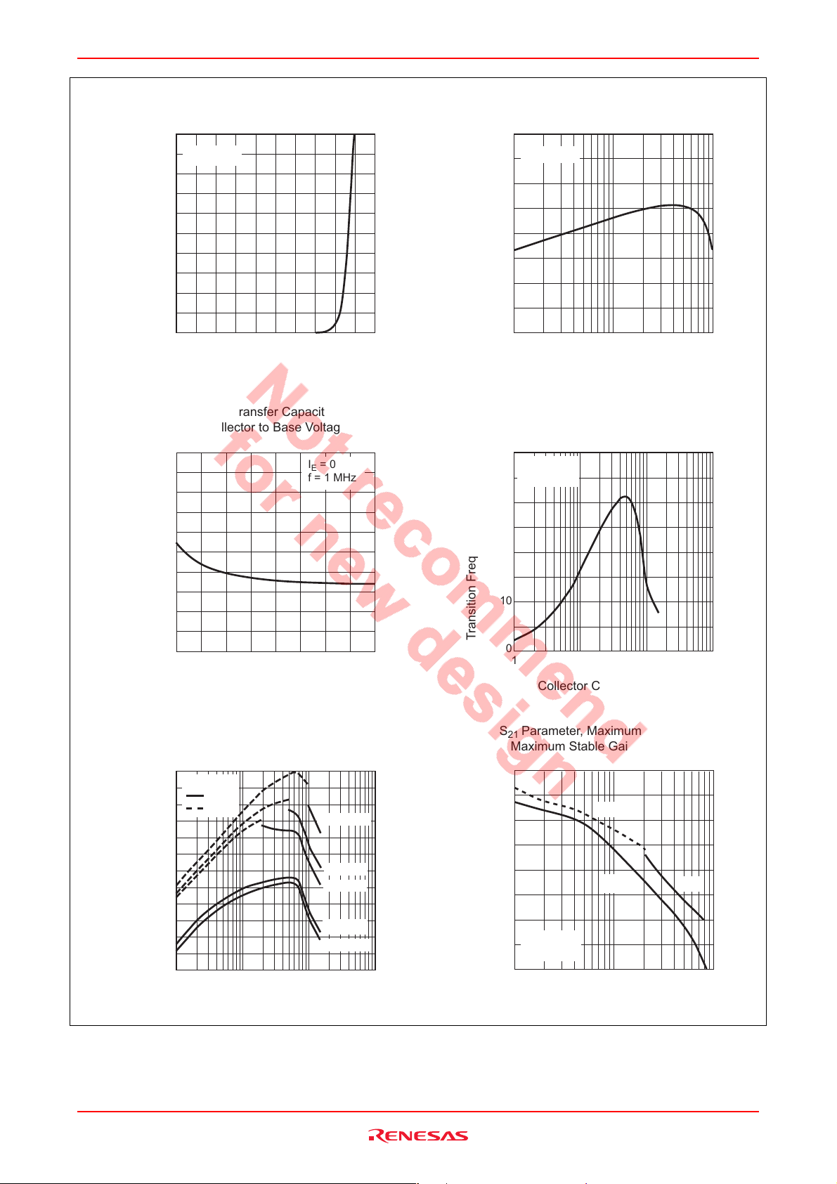
HSG2004
100
(mA)
C
Typical Transfer Characteristics
VCE = 3 V
80
60
40
(-)
FE
DC Current Transfer Ratio vs.
Collector Current
400
VCE = 3 V
300
200
20
Collector Current I
0 0.2 0.4 0.6 0.8 1.0
Base to Emitter Voltage VBE (V)
Reverse Transfer Capacitanse vs.
Collector to Base Voltage
0.5
(pF)
re
0.4
0.3
0.2
0.1
0
Reverse Transfer Capacitanse C
1234
I
E
f = 1 MHz
Collector to Base Voltage VCB (V)
= 0
100
DC Current Transfer Ratio h
0
1 10 100
Collector Current IC (mA)
Transition Frequency vs.
Collector Current
40
VCE = 3 V
f = 1 GHz
(GHz)
30
T
20
10
Transition Frequency f
0
1 10 100 1000
Collector Current IC (mA)
Maximum Stable Gain, Maximum Available Gain
vs. Collector Current
30
VCE = 3 V
MAG
25
MSG
20
15
10
5
Maximum Stable Gain MSG (dB)
0
Maximum Available Gain MAG (dB)
1 10 100 1000
Collector Current I
Rev.4.00 Jun 21, 2006 page 3 of 12
f = 1 GHz
1.8 GHz
2.4 GHz
5.2 GHz
5.8 GHz
(mA)
C
S
Parameter, Maximum Available Gain,
21
Maximum Stable Gain vs. Frequency
40
(dB)
2
|
|S
Parameter
S
30
21
20
10
21
Maximum Stable Gain MSG (dB)
VCE = 3 V
I
= 30 mA
C
0
Maximum Available Gain MAG (dB)
0.1 1 10
MSG
|S21|
Frequency f (GHz)
2
MAG
Page 4
HSG2004
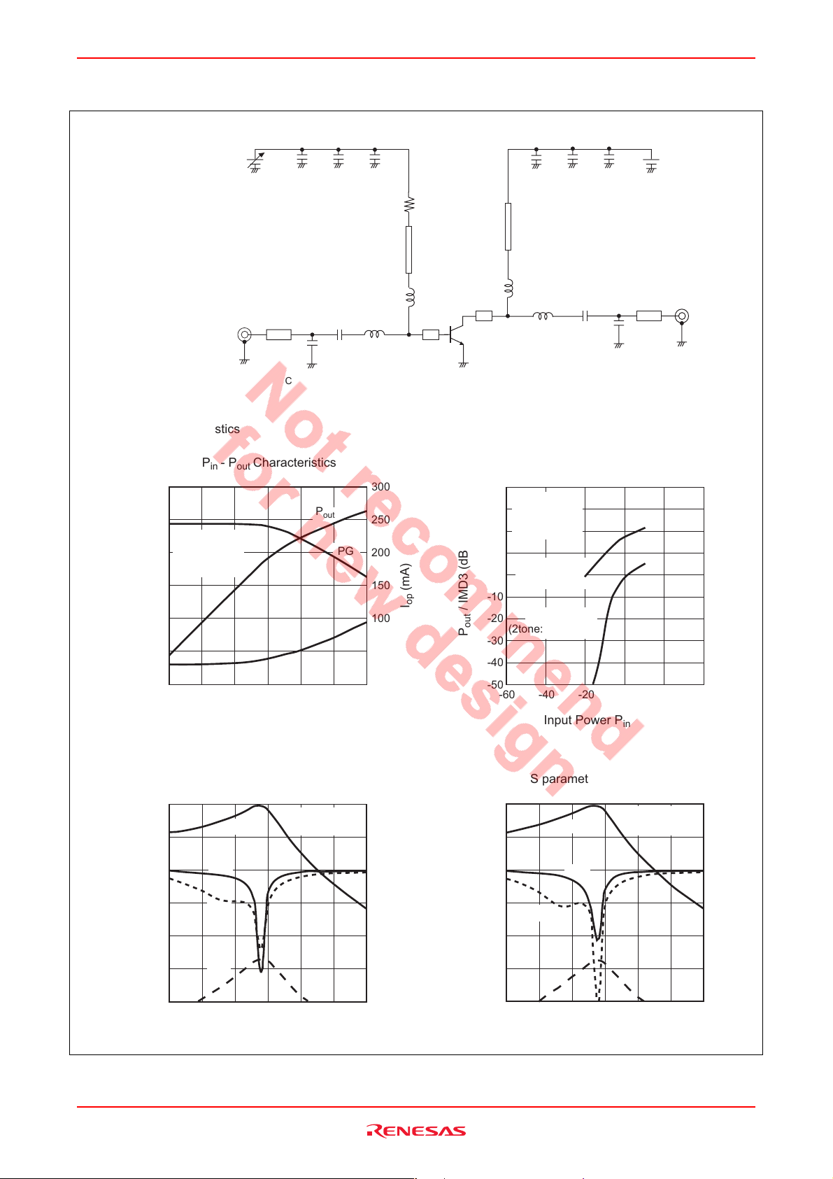
2.4 GHz Characteristics
Evaluation Board Circuit
VBB:Bias Control
P
- P
Characteristics
in
out
25
20
VCC = 3.6 V
(dBm)
out
15
I
idle
f = 2.4 GHz
10
5
Power Gain PG (dB)
Output Power P
0
-5
-20
IN
P
- P
in
= 30 mA
Characteristics
out
-10
1000 pF*1 µF 10 pF
C : 1 to 2 pF
P
out
I
op
0
C : 1 pF
PG
R : 27 Ω
L : 5.6 nH
L : 1.5 nH
300
250
200
150
100
50
0
10
(mA)
op
I
10 pF
L : 10 nH
L : 1.8 nH
1000 pF
C : 2 pF
*1 µF
C : 0.9 pF
VCC
3rd. Order Intermodulation Distortion (IMD3)
40
VCE = 3.6 V
30
I
= 30 mA
idle
f = 2.4 GHz
20
10
Fundamental
0
(1tone)
-10
/ IMD3 (dBm)
-20
out
P
-30
-40
-50
IMD3
(2tone: ∆f = 1MHz)
-40 0 40-20-60
20
OUT
Input Power P
S parameter vs. Frequency
20
10
0
-10
-20
S parameter (dB)
-30
-40
S21
S11
S22
S12
2.0 3.5
1.5 3.0 4.02.51.0
Frequency f (GHz)
Rev.4.00 Jun 21, 2006 page 4 of 12
(dBm)
in
VCE = 3.6 V
I
= 30 mA
C
Input Power Pin (dBm)
S parameter vs. Frequency
20
10
0
-10
S22
-20
S parameter (dB)
-30
-40
1.0
S12
1.5 3.0 4.02.5
S21
I
C
S11
2.0 3.5
Frequency f (GHz)
VCE = 3.6 V
= 40 mA
Page 5

HSG2004
5.8 GHz Characteristics
Evaluation Board Circuit
VBB:Bias Control
P
- P
Characteristics
in
out
25
VCC = 3.6 V
I
20
f = 5.8 GHz
(dBm)
out
15
10
Power Gain PG (dB)
Output Power P
5
= 30 mA
idle
VCC
1000 pF
*1 µF
1000 pF
IN
P
- P
in
Characteristics
out
P
out
0.5 pF
I
op
PG
2 pF
10 pF
0.3 pF
250
200
150
100
50
20 Ω
(mA)
op
I
10 pF
2 pF
0.5 pF
0.5 pF
3rd. Order Intermodulation Distortion (IMD3)
40
VCE = 3.6 V
I
= 30 mA
idle
20
f = 5.8 GHz
0
Fundamental
-20
/ IMD3 (dBm)
out
P
-40
(1tone)
(2tone:∆f = 1MHz)
*1 µF
OUT
IMD3
0
-20
-10
Input Power P
S parameter vs. Frequency
20
VCE = 3.6 V
I
= 30 mA
C
10
0
-10
S22
S parameter (dB)
-20
S12
-30
57864
(dBm)
in
S21
S11
Frequency f (GHz)
10 200
0
-60
-40 0 40-20-60
20
Input Power Pin (dBm)
S parameter vs. Frequency
20
VCE = 3.6 V
I
= 40 mA
C
10
-10
0
S11
S22
S21
S parameter (dB)
-20
S12
-30
57864
Frequency f (GHz)
Rev.4.00 Jun 21, 2006 page 5 of 12
Page 6

HSG2004
S
Parameter vs. Frequency
11
1
.4
.2
0
-.2
.2
-.4
Condition: V
.8
.6
.6
.4
.8
-.6
-.8
-1
= 3 V, IC = 30 mA, Zo = 50 Ω
CE
1.5
2
3
4
5
10
1.5
234
1
-1.5
10
5
-10
-5
-4
-3
-2
100 to 3000 MHz (100 MHz Step)
3200 to 6000 MHz (200 MHz Step)
Parameter vs. Frequency
S
21
Scale: 14 / div.
60°
-30°
-60°
150°
180°
-150°
Condition: V
90°
120°
-120°
-90°
= 3 V, IC = 30 mA, Zo = 50 Ω
CE
100 to 3000 MHz (100 MHz Step)
3200 to 6000 MHz (200 MHz Step)
30°
0°
Parameter vs. Frequency S22 Parameter vs. Frequency
S
150°
180°
-150°
Condition: V
12
120°
-120°
CE
-90°
= 3 V, IC = 30 mA, Zo = 50 Ω
90°
Scale: 0.04 / div.
60°
30°
-30°
-60°
100 to 3000 MHz (100 MHz Step)
3200 to 6000 MHz (200 MHz Step)
1
.8
.6
.4
.2
0°
0
-.2
.2
-.4
Condition: V
.6
.4
.8
-.6
-.8
-1
= 3 V, IC = 30 mA, Zo = 50 Ω
CE
1.5
2
3
4
5
10
1.5
234
1
-1.5
10
5
-10
-5
-4
-3
-2
100 to 3000 MHz (100 MHz Step)
3200 to 6000 MHz (200 MHz Step)
Rev.4.00 Jun 21, 2006 page 6 of 12
Page 7

HSG2004
S
Parameter vs. Frequency
11
1
.4
.2
0
-.2
.2
-.4
Condition: V
.8
.6
.6
.4
.8
-.6
-.8
-1
= 3.3 V, IC = 30 mA, Zo = 50 Ω
CE
1.5
2
3
4
5
10
1.5
234
1
-1.5
10
5
-10
-5
-4
-3
-2
100 to 3000 MHz (100 MHz Step)
3200 to 6000 MHz (200 MHz Step)
Parameter vs. Frequency
S
21
Scale: 14 / div.
60°
-30°
-60°
150°
180°
-150°
Condition: V
90°
120°
-120°
-90°
= 3.3 V, IC = 30 mA, Zo = 50 Ω
CE
100 to 3000 MHz (100 MHz Step)
3200 to 6000 MHz (200 MHz Step)
30°
0°
Parameter vs. Frequency S22 Parameter vs. Frequency
S
150°
180°
-150°
Condition: V
12
120°
-120°
CE
-90°
= 3.3 V, IC = 30 mA, Zo = 50 Ω
90°
Scale: 0.04 / div.
60°
30°
-30°
-60°
100 to 3000 MHz (100 MHz Step)
3200 to 6000 MHz (200 MHz Step)
1
.8
.6
.4
.2
0°
0
-.2
.2
-.4
Condition: V
.6
.4
.8
-.6
-.8
-1
= 3.3 V, IC = 30 mA, Zo = 50 Ω
CE
1.5
2
3
4
5
10
1.5
234
1
-1.5
10
5
-10
-5
-4
-3
-2
100 to 3000 MHz (100 MHz Step)
3200 to 6000 MHz (200 MHz Step)
Rev.4.00 Jun 21, 2006 page 7 of 12
Page 8
HSG2004
S
Parameter vs. Frequency
11
1
.4
.2
0
-.2
.2
-.4
Condition: V
.8
.6
.6
.4
.8
-.6
-.8
-1
= 3.6 V, IC = 30 mA, Zo = 50 Ω
CE
1.5
2
3
4
5
10
1.5
234
1
-1.5
10
5
-10
-5
-4
-3
-2
100 to 3000 MHz (100 MHz Step)
3200 to 6000 MHz (200 MHz Step)
Parameter vs. Frequency
S
21
Scale: 14 / div.
60°
-30°
-60°
150°
180°
-150°
Condition: V
90°
120°
-120°
-90°
= 3.6 V, IC = 30 mA, Zo = 50 Ω
CE
100 to 3000 MHz (100 MHz Step)
3200 to 6000 MHz (200 MHz Step)
30°
0°
Parameter vs. Frequency S22 Parameter vs. Frequency
S
150°
180°
-150°
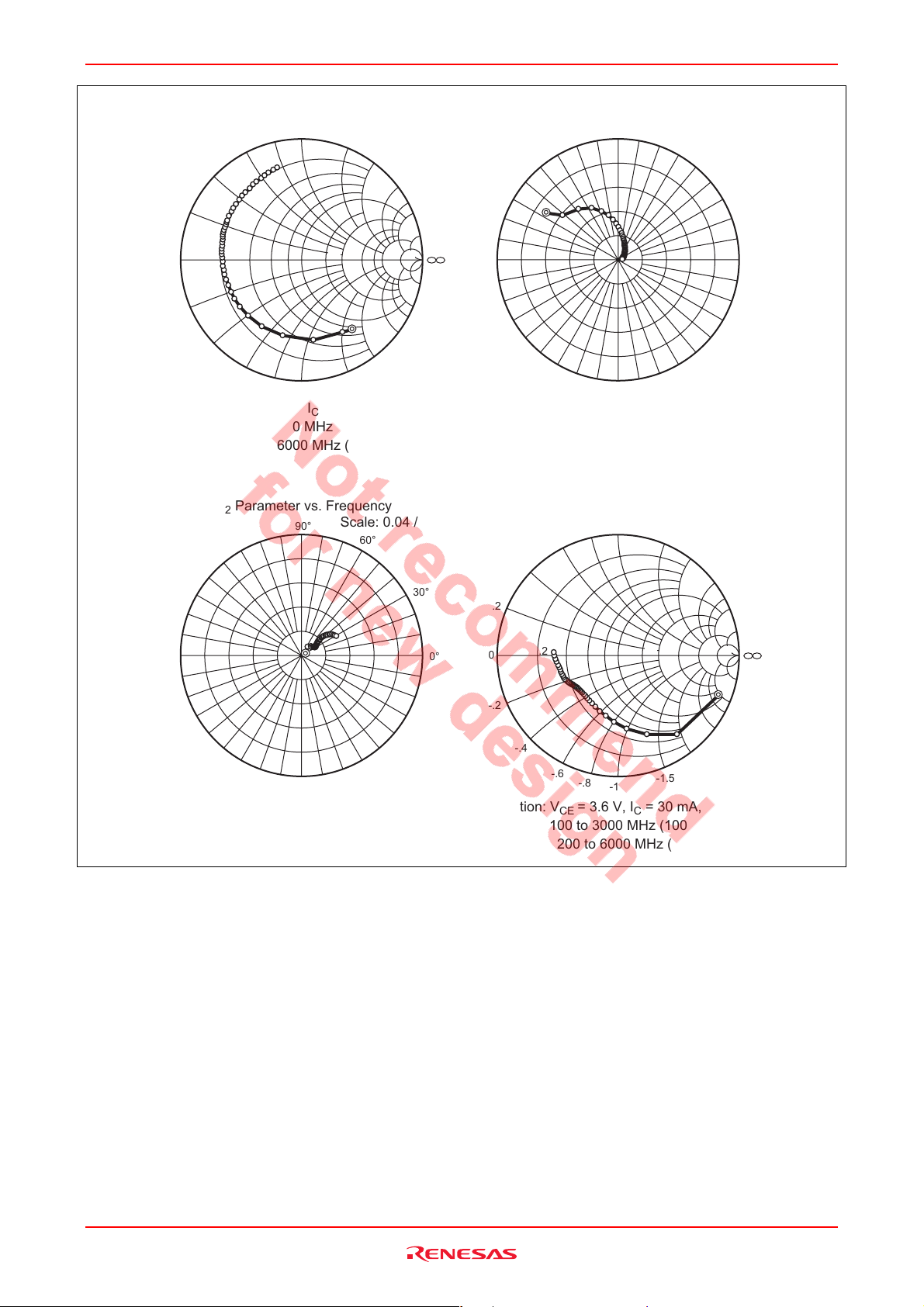
Condition: V
12
120°
-120°
CE
-90°
= 3.6 V, IC = 30 mA, Zo = 50 Ω
90°
Scale: 0.04 / div.
60°
30°
-30°
-60°
100 to 3000 MHz (100 MHz Step)
3200 to 6000 MHz (200 MHz Step)
1
.8
.6
.4
.2
0°
0
-.2
.2
-.4
Condition: V
.6
.4
.8
-.6
-.8
-1
= 3.6 V, IC = 30 mA, Zo = 50 Ω
CE
1.5
2
3
4
5
10
1.5
234
1
-1.5
10
5
-10
-5
-4
-3
-2
100 to 3000 MHz (100 MHz Step)
3200 to 6000 MHz (200 MHz Step)
Rev.4.00 Jun 21, 2006 page 8 of 12
Page 9

HSG2004
S parameter
(VCE = 3 V, IC = 30 mA, Zo = 50 Ω)
f (MHz)
100 0.684 -61.3 47.90 147.5 0.0103 39.8 1.006 -19.0
200 0.708 -53.6 39.45 142.1 0.0168 50.5 0.811 -53.9
300 0.664 -81.8 35.97 128.9 0.0180 41.9 0.685 -71.2
400 0.644 -105.0 32.90 117.8 0.0192 36.7 0.601 -84.9
500 0.638 -121.4 29.04 109.5 0.0214 34.3 0.543 -94.8
600 0.640 -134.8 25.80 102.8 0.0225 31.8 0.505 -102.7
700 0.640 -143.6 22.83 97.7 0.0240 29.2 0.480 -109.5
800 0.640 -150.6 20.30 93.4 0.0238 28.5 0.460 -115.0
900 0.641 -156.5 18.23 89.8 0.0242 30.5 0.447 -119.7
1000 0.641 -161.6 16.44 86.5 0.0249 30.4 0.437 -123.8
1100 0.644 -166.1 15.00 83.6 0.0250 27.9 0.431 -127.3
1200 0.648 -169.8 13.75 80.9 0.0252 29.1 0.427 -130.2
1300 0.649 -173.1 12.70 78.4 0.0258 29.4 0.425 -132.7
1400 0.651 -176.2 11.78 76.0 0.0262 29.7 0.423 -134.9
1500 0.651 -179.2 10.97 73.9 0.0263 30.7 0.423 -136.9
1600 0.656 177.9 10.23 71.8 0.0270 32.4 0.424 -138.7
1700 0.660 175.5 9.58 69.9 0.0274 33.0 0.425 -140.3
1800 0.665 173.5 9.01 68.0 0.0282 33.6 0.427 -141.7
1900 0.667 171.5 8.52 66.1 0.0285 34.5 0.429 -143.0
2000 0.668 169.3 8.08 64.1 0.0294 34.3 0.432 -144.1
2100 0.669 167.1 7.65 62.4 0.0297 35.2 0.435 -145.2
2200 0.673 164.9 7.27 60.7 0.0304 35.9 0.438 -146.2
2300 0.678 163.1 6.92 59.2 0.0310 36.5 0.441 -147.3
2400 0.683 161.5 6.61 57.6 0.0318 37.7 0.444 -148.0
2500 0.687 160.0 6.32 55.9 0.0327 38.0 0.448 -148.9
2600 0.687 158.2 6.05 54.2 0.0337 37.6 0.450 -149.6
2700 0.688 156.4 5.80 52.5 0.0339 38.8 0.454 -150.3
2800 0.689 154.5 5.57 50.9 0.0348 38.8 0.457 -150.9
2900 0.693 152.9 5.35 49.5 0.0359 39.4 0.460 -151.6
3000 0.698 151.5 5.16 48.2 0.0364 39.9 0.463 -152.2
3200 0.702 148.6 4.80 45.0 0.0381 40.5 0.468 -153.4
3400 0.703 145.0 4.48 41.8 0.0399 40.5 0.473 -154.6
3600 0.709 142.1 4.19 39.0 0.0418 40.7 0.477 -156.0
3800 0.712 139.0 3.95 36.0 0.0436 40.1 0.480 -157.3
4000 0.715 135.4 3.72 32.7 0.0453 39.9 0.483 -158.9
4200 0.723 132.3 3.51 29.9 0.0477 39.2 0.485 -160.6
4400 0.726 129.2 3.33 27.0 0.0489 39.3 0.487 -162.5
4600 0.730 125.4 3.14 23.7 0.0511 38.3 0.490 -164.8
4800 0.742 122.4 2.98 20.8 0.0531 37.1 0.493 -167.0
5000 0.747 119.4 2.84 17.8 0.0555 36.5 0.497 -169.5
5200 0.753 115.9 2.69 14.5 0.0571 35.1 0.503 -172.1
5400 0.765 113.0 2.55 11.5 0.0592 33.4 0.509 -174.9
5600 0.773 110.3 2.43 8.4 0.0612 31.6 0.517 -177.8
5800 0.779 106.9 2.30 5.3 0.0628 30.0 0.525 179.3
6000 0.790 104.5 2.18 2.2 0.0643 28.2 0.534 176.2
MAG ANG (deg.) MAG ANG (deg.) MAG ANG (deg.) MAG ANG (deg.)
S11 S21 S12 S22
Rev.4.00 Jun 21, 2006 page 9 of 12
Page 10

HSG2004
S parameter
(VCE = 3.3 V, IC = 30 mA, Zo = 50 Ω)
f (MHz)
100 0.674 -60.3 48.82 147.33 0.0124 106.4 0.755 -22.6
200 0.708 -53.6 40.51 141.98 0.0146 57.5 0.814 -53.5
300 0.668 -81.6 36.68 128.82 0.0189 39.9 0.690 -70.4
400 0.646 -104.3 33.30 117.87 0.0211 42.3 0.598 -83.9
500 0.637 -121.1 29.33 109.63 0.0216 34.1 0.544 -94.1
600 0.638 -134.3 26.04 102.93 0.0229 32.8 0.506 -102.0
700 0.640 -143.1 23.01 97.82 0.0234 31.7 0.480 -108.7
800 0.639 -150.2 20.48 93.51 0.0239 29.8 0.460 -114.2
900 0.639 -156.1 18.38 89.85 0.0244 30.0 0.448 -119.1
1000 0.639 -161.2 16.56 86.63 0.0247 28.7 0.436 -123.2
1100 0.643 -165.7 15.11 83.71 0.0248 29.6 0.431 -126.6
1200 0.647 -169.5 13.85 80.95 0.0252 27.6 0.426 -129.5
1300 0.648 -172.8 12.80 78.44 0.0259 30.7 0.424 -132.0
1400 0.649 -175.9 11.87 76.09 0.0258 30.7 0.422 -134.3
1500 0.650 -178.9 11.05 73.89 0.0269 31.0 0.422 -136.4
1600 0.653 178.2 10.31 71.81 0.0273 32.5 0.423 -138.2
1700 0.658 175.8 9.66 69.89 0.0276 31.8 0.424 -139.8
1800 0.663 173.7 9.08 67.99 0.0281 33.4 0.426 -141.2
1900 0.665 171.7 8.58 66.10 0.0288 34.3 0.428 -142.5
2000 0.667 169.5 8.14 64.14 0.0294 35.0 0.431 -143.6
2100 0.667 167.3 7.71 62.39 0.0297 35.5 0.434 -144.8
2200 0.671 165.1 7.33 60.67 0.0305 35.8 0.437 -145.7
2300 0.676 163.3 6.97 59.20 0.0311 36.7 0.440 -146.7
2400 0.682 161.6 6.66 57.56 0.0318 37.6 0.443 -147.6
2500 0.685 160.1 6.36 55.90 0.0322 37.5 0.447 -148.4
2600 0.685 158.4 6.10 54.14 0.0337 39.1 0.450 -149.2
2700 0.687 156.5 5.85 52.44 0.0342 38.8 0.453 -149.8
2800 0.688 154.7 5.61 50.90 0.0348 39.2 0.456 -150.6
2900 0.692 153.1 5.39 49.52 0.0355 39.3 0.459 -151.2
3000 0.696 151.6 5.19 48.15 0.0361 39.5 0.462 -151.8
3200 0.701 148.7 4.84 44.97 0.0380 40.5 0.467 -153.0
3400 0.702 145.2 4.51 41.72 0.0397 40.5 0.472 -154.2
3600 0.708 142.3 4.22 39.02 0.0414 40.1 0.476 -155.6
3800 0.710 139.2 3.98 35.99 0.0437 41.0 0.479 -156.9
4000 0.714 135.5 3.75 32.71 0.0458 40.5 0.483 -158.5
4200 0.722 132.4 3.54 29.88 0.0477 39.9 0.484 -160.3
4400 0.724 129.4 3.35 26.99 0.0490 38.8 0.487 -162.2
4600 0.729 125.5 3.17 23.61 0.0509 38.5 0.489 -164.4
4800 0.740 122.4 3.01 20.69 0.0530 37.5 0.493 -166.7
5000 0.746 119.5 2.86 17.76 0.0554 36.7 0.497 -169.1
5200 0.752 115.9 2.71 14.45 0.0573 35.6 0.502 -171.7
5400 0.764 113.1 2.57 11.42 0.0592 33.8 0.509 -174.6
5600 0.773 110.4 2.45 8.38 0.0614 31.9 0.516 -177.5
5800 0.778 107.0 2.32 5.20 0.0623 30.6 0.524 179.6
6000 0.789 104.5 2.19 2.09 0.0639 28.1 0.534 176.6
MAG ANG (deg.) MAG ANG (deg.) MAG ANG (deg.) MAG ANG (deg.)
S11 S21 S12 S22
Rev.4.00 Jun 21, 2006 page 10 of 12
Page 11

HSG2004
S parameter
(VCE = 3.6 V, IC = 30 mA, Zo = 50 Ω)
f (MHz)
100 0.686 -60.1 49.50 147.35 0.0070 30.5 0.897 -21.2
200 0.713 -53.6 41.32 141.93 0.0155 53.8 0.815 -52.9
300 0.669 -81.1 37.11 128.90 0.0200 42.6 0.690 -69.6
400 0.645 -103.8 33.55 118.06 0.0199 37.3 0.605 -83.3
500 0.637 -120.5 29.52 109.81 0.0221 34.8 0.546 -93.3
600 0.638 -133.6 26.17 103.15 0.0222 31.6 0.507 -101.4
700 0.638 -142.5 23.13 98.02 0.0238 30.5 0.481 -108.1
800 0.637 -149.7 20.59 93.66 0.0239 28.3 0.461 -113.7
900 0.638 -155.6 18.47 90.02 0.0243 28.8 0.447 -118.4
1000 0.638 -160.8 16.65 86.77 0.0245 29.0 0.437 -122.5
1100 0.642 -165.3 15.20 83.83 0.0251 29.2 0.431 -125.9
1200 0.645 -169.1 13.93 81.07 0.0256 29.2 0.427 -129.0
1300 0.645 -172.4 12.87 78.55 0.0253 30.2 0.424 -131.4
1400 0.648 -175.6 11.94 76.19 0.0263 30.9 0.423 -133.8
1500 0.648 -178.6 11.11 73.98 0.0268 30.6 0.422 -135.8
1600 0.652 178.5 10.37 71.89 0.0271 32.1 0.423 -137.7
1700 0.657 176.1 9.71 69.97 0.0274 32.5 0.424 -139.3
1800 0.662 174.0 9.13 68.06 0.0279 33.0 0.426 -140.7
1900 0.664 171.9 8.62 66.16 0.0287 33.5 0.428 -142.1
2000 0.665 169.8 8.18 64.18 0.0292 34.2 0.431 -143.2
2100 0.666 167.5 7.75 62.44 0.0298 34.7 0.433 -144.3
2200 0.670 165.3 7.37 60.71 0.0306 35.9 0.436 -145.4
2300 0.675 163.5 7.01 59.24 0.0310 36.8 0.439 -146.3
2400 0.680 161.9 6.69 57.59 0.0316 36.8 0.443 -147.1
2500 0.684 160.4 6.40 55.92 0.0322 37.7 0.446 -148.0
2600 0.683 158.7 6.13 54.16 0.0335 38.0 0.450 -148.8
2700 0.684 156.8 5.88 52.46 0.0338 39.0 0.453 -149.5
2800 0.686 154.9 5.64 50.91 0.0345 39.3 0.455 -150.1
2900 0.691 153.2 5.42 49.54 0.0349 39.4 0.459 -150.8
3000 0.695 151.8 5.22 48.16 0.0364 39.8 0.462 -151.4
3200 0.700 148.9 4.86 44.99 0.0383 40.4 0.467 -152.5
3400 0.700 145.3 4.53 41.72 0.0399 40.5 0.472 -153.9
3600 0.706 142.4 4.24 39.01 0.0420 40.3 0.476 -155.2
3800 0.709 139.3 4.00 36.00 0.0430 40.9 0.479 -156.6
4000 0.713 135.6 3.77 32.71 0.0452 40.3 0.482 -158.1
4200 0.721 132.6 3.56 29.88 0.0471 40.2 0.485 -159.9
4400 0.723 129.5 3.37 26.99 0.0489 39.2 0.487 -161.8
4600 0.728 125.6 3.18 23.59 0.0510 38.4 0.489 -164.0
4800 0.739 122.6 3.02 20.67 0.0527 37.6 0.492 -166.4
5000 0.745 119.7 2.87 17.72 0.0551 36.4 0.496 -168.8
5200 0.751 116.1 2.72 14.42 0.0573 35.6 0.502 -171.4
5400 0.762 113.2 2.58 11.39 0.0590 33.7 0.509 -174.3
5600 0.771 110.4 2.46 8.34 0.0610 32.0 0.516 -177.2
5800 0.777 107.1 2.33 5.17 0.0624 30.4 0.524 179.8
6000 0.788 104.7 2.21 2.04 0.0638 28.5 0.533 176.8
MAG ANG (deg.) MAG ANG (deg.) MAG ANG (deg.) MAG ANG (deg.)
S11 S21 S12 S22
Rev.4.00 Jun 21, 2006 page 11 of 12
Page 12
HSG2004
Package Dimensions
Package Name
HWQFN-8
B
E
S
P-HWQFN8-2x2-0.65 PWQN0008ZA-A TNP-8TV 0.009g
D
76
8448
1
2
5
3
y
1
y
S
A
S
A
1
A
MASS[Typ.]RENESAS CodeJEITA Package Code Previous Code
b
5
E
Z
32
Z
D
6
0.90
C0.15
MxSA
B
7
1
e
p
L
0.05
0.60
Dimension in Millimeters
Reference
Symbol
Min Nom Max
1.965
D
1.965
E
A
A
1
A
2
b
e
L
p
x
y
y
1
Z
D
Z
E
2.00
2.075
2.00
2.075
0.80
0
0.05
0.3
0.65
0.35
0.10
0.08
0.10
0.350
0.225
Ordering Information
Part Name Quantity Shipping Container
HSG2004TB-E 2000 pcs. φ178 mm Reel, 8 mm Emboss Taping
Note: Therefore especially small contact area of terminal, miss contact may occur if inadequate soldering condition is
applied.
Contact Renesas sales office for any question regarding recommended soldering conditio n of Renesas.
Rev.4.00 Jun 21, 2006 page 12 of 12
Page 13
Sales Strategic Planning Div. Nippon Bldg., 2-6-2, Ohte-machi, Chiyoda-ku, Tokyo 100-0004, Japan
Keep safety first in your circuit designs!
1. Renesas Technology Corp. puts the maximum effort into making semiconductor products better and more reliable, but there is always the possibility that trouble
may occur with them. Trouble with semiconductors may lead to personal injury, fire or property damage.
Remember to give due consideration to safety when making your circuit designs, with appropriate measures such as (i) placement of substitutive, auxiliary
circuits, (ii) use of nonflammable material or (iii) prevention against any malfunction or mishap.
Notes regarding these materials
1. These materials are intended as a reference to assist our customers in the selection of the Renesas Technology Corp. product best suited to the customer's
application; they do not convey any license under any intellectual property rights, or any other rights, belonging to Renesas Technology Corp. or a third party.
2. Renesas Technology Corp. assumes no responsibility for any damage, or infringement of any third-party's rights, originating in the use of any product data,
diagrams, charts, programs, algorithms, or circuit application examples contained in these materials.
3. All information contained in these materials, including product data, diagrams, charts, programs and algorithms represents information on products at the time of
publication of these materials, and are subject to change by Renesas Technology Corp. without notice due to product improvements or other reasons. It is
therefore recommended that customers contact Renesas Technology Corp. or an authorized Renesas Technology Corp. product distributor for the latest product
information before purchasing a product listed herein.
The information described here may contain technical inaccuracies or typographical errors.
Renesas Technology Corp. assumes no responsibility for any damage, liability, or other loss rising from these inaccuracies or errors.
Please also pay attention to information published by Renesas Technology Corp. by various means, including the Renesas Technology Corp. Semiconductor
home page (http://www.renesas.com).
4. When using any or all of the information contained in these materials, including product data, diagrams, charts, programs, and algorithms, please be sure to
evaluate all information as a total system before making a final decision on the applicability of the information and products. Renesas Technology Corp. assumes
no responsibility for any damage, liability or other loss resulting from the information contained herein.
5. Renesas Technology Corp. semiconductors are not designed or manufactured for use in a device or system that is used under circumstances in which human life
is potentially at stake. Please contact Renesas Technology Corp. or an authorized Renesas Technology Corp. product distributor when considering the use of a
product contained herein for any specific purposes, such as apparatus or systems for transportation, vehicular, medical, aerospace, nuclear, or undersea repeater
use.
6. The prior written approval of Renesas Technology Corp. is necessary to reprint or reproduce in whole or in part these materials.
7. If these products or technologies are subject to the Japanese export control restrictions, they must be exported under a license from the Japanese government and
cannot be imported into a country other than the approved destination.
Any diversion or reexport contrary to the export control laws and regulations of Japan and/or the country of destination is prohibited.
8. Please contact Renesas Technology Corp. for further details on these materials or the products contained therein.
RENESAS SALES OFFICES
http://www.renesas.com
Refer to "http://www.renesas.com/en/network" for the latest and detailed information.
Renesas Technology America, Inc.
450 Holger Way, San Jose, CA 95134-1368, U.S.A
Tel: <1> (408) 382-7500, Fax: <1> (408) 382-7501
Renesas Technology Europe Limited
Dukes Meadow, Millboard Road, Bourne End, Buckinghamshire, SL8 5FH, U.K.
Tel: <44> (1628) 585-100, Fax: <44> (1628) 585-900
Renesas Technology (Shanghai) Co., Ltd.
Unit 204, 205, AZIACenter, No.1233 Lujiazui Ring Rd, Pudong District, Shanghai, China 200120
Tel: <86> (21) 5877-1818, Fax: <86> (21) 6887-7898
Renesas Technology Hong Kong Ltd.
7th Floor, North Tower, World Finance Centre, Harbour City, 1 Canton Road, Tsimshatsui, Kowloon, Hong Kong
Tel: <852> 2265-6688, Fax: <852> 2730-6071
Renesas Technology Taiwan Co., Ltd.
10th Floor, No.99, Fushing North Road, Taipei, Taiwan
Tel: <886> (2) 2715-2888, Fax: <886> (2) 2713-2999
Renesas Technology Singapore Pte. Ltd.
1 Harbour Front Avenue, #06-10, Keppel Bay Tower, Singapore 098632
Tel: <65> 6213-0200, Fax: <65> 6278-8001
Renesas Technology Korea Co., Ltd.
Kukje Center Bldg. 18th Fl., 191, 2-ka, Hangang-ro, Yongsan-ku, Seoul 140-702, Korea
Tel: <82> (2) 796-3115, Fax: <82> (2) 796-2145
Renesas Technology Malaysia Sdn. Bhd
Unit 906, Block B, Menara Amcorp, Amcorp Trade Centre, No.18, Jalan Persiaran Barat, 46050 Petaling Jaya, Selangor Darul Ehsan, Malaysia
Tel: <603> 7955-9390, Fax: <603> 7955-9510
© 2006. Renesas Technology Corp., All rights reserved. Printed in Japan.
Colophon .6.0
 Loading...