

Page 1

查询HN58V65AFPI-10供应商
HN58V65AI Series
HN58V66AI Series
HN58V65A-SR Series
HN58V66A-SR Series
64k EEPROM (8-kword × 8-bit)
Ready/Busy function, RES function (HN58V66A)
Wide Temperature Range version
REJ03C0153-0300Z
(Previous ADE-203-759B(Z) Rev.2.0)
Rev. 3.00
Feb.02.2004
Description
Renesas Technology’s HN58V65A series and HN58V66A series are electrically erasable and
programmable EEPROM’s organized as 8192-word × 8-bit. They have realized high speed, low power
consumption and high reliability by employing advanced MNOS memory technology and CMOS process
and circuitry technology. They also have a 64-byte page programming function to make their write
operations faster.
Features
• Single supply: 2.7 to 5.5 V
• Access time:
100 ns (max) at 2.7 V ≤ V
70 ns (max) at 4.5 V ≤ V
• Power dissipation:
Active: 20 mW/MHz (typ)
Standby: 110 µW (max)
• On-chip latches: address, data, CE, OE, WE
• Automatic byte write: 10 ms (max)
• Automatic page write (64 bytes): 10 ms (max)
• Ready/Busy
• Data polling and Toggle bit
• Data protection circuit on power on/off
< 4.5 V
CC
≤ 5.5 V
CC
Rev.3.00, Feb.02.2004, page 1 of 26
Page 2

HN58V65AI/HN58V66AI/HN58V65A-SR/HN58V66A-SR Series
Features (cont)
• Conforms to JEDEC byte-wide standard
• Reliable CMOS with MNOS cell technology
5
• 10
erase/write cycles (in page mode)
• 10 years data retention
• Software data protection
• Write protection by RES pin (only the HN58V66A series)
• Operating temperature range:
HN58V65AI/HN58V66AI Series: −40 to +85°C
HN58V65A-SR/HN58V66A-SR Series: −20 to +85°C
• There are also lead free products.
Ordering Information
Access time
Type No. 2.7 V ≤ VCC < 4.5 V 4.5 V ≤ VCC ≤ 5.5 V Package
HN58V65API-10 100 ns 70 ns 600 mil 28-pin plastic DIP (DP-28)
HN58V66API-10 100 ns 70 ns
HN58V65AFPI-10 100 ns 70 ns 400 mil 28-pin plastic SOP (FP-28D)
HN58V66AFPI-10 100 ns 70 ns
HN58V65ATI-10 100 ns 70 ns 28-pin plastic TSOP(TFP-28DB)
HN58V66ATI-10 100 ns 70 ns
HN58V65AT-10SR 100 ns 70 ns
HN58V66AT-10SR 100 ns 70 ns
HN58V65API-10E 100 ns 70 ns 600 mil 28-pin plastic DIP (DP-28V)
HN58V66API-10E 100 ns 70 ns Lead free
HN58V65AFPI-10E 100 ns 70 ns 400 mil 28-p in plastic SOP (FP-28DV)
HN58V66AFPI-10E 100 ns 70 ns Lead free
HN58V65ATI-10E 100 ns 70 ns 28-pin plastic TSOP(TFP-28DBV)
HN58V66ATI-10E 100 ns 70 ns Lead free
HN58V65AT-10SRE 100 ns 70 ns
HN58V66AT-10SRE 100 ns 70 ns
Rev.3.00, Feb.02.2004, page 2 of 26
Page 3

HN58V65AI/HN58V66AI/HN58V65A-SR/HN58V66A-SR Series
Pin Arrangement
HN58V65API Series
HN58V65AFPI Series
RDY/Busy
A12
A7
A6
A5
A4
A3
A2
A1
A0
I/O0
I/O1
I/O2
V
SS
RDY/Busy
A12
A7
A6
A5
A4
A3
A2
A1
A0
I/O0
I/O1
I/O2
V
SS
1
2
3
4
5
6
7
8
9
10
11
12
13
14
(Top view)
HN58V66API Series
HN58V66AFPI Series
1
2
3
4
5
6
7
8
9
10
11
12
13
14
28
27
26
25
24
23
22
21
20
19
18
17
16
15
28
27
26
25
24
23
22
21
20
19
18
17
16
15
V
CC
WE
NC
A8
A9
A11
OE
A10
CE
I/O7
I/O6
I/O5
I/O4
I/O3
V
CC
WE
RES
A8
A9
A11
OE
A10
CE
I/O7
I/O6
I/O5
I/O4
I/O3
A2
A1
A0
I/O0
I/O1
I/O2
V
I/O3
I/O4
I/O5
I/O6
I/O7
CE
A10
A2
A1
A0
I/O0
I/O1
I/O2
V
I/O3
I/O4
I/O5
I/O6
I/O7
CE
A10
HN58V65ATI Series
HN58V65AT-SR Series
15
16
17
18
19
20
21
SS
22
23
24
25
26
27
28
14
13
12
11
10
9
8
7
6
5
4
3
2
1
A3
A4
A5
A6
A7
A12
RDY/Busy
V
CC
WE
NC
A8
A9
A11
OE
(Top view)
HN58V66ATI Series
HN58V66AT-SR Series
15
16
17
18
19
20
21
SS
22
23
24
25
26
27
28
14
13
12
11
10
9
8
7
6
5
4
3
2
1
A3
A4
A5
A6
A7
A12
RDY/Busy
V
CC
WE
RES
A8
A9
A11
OE
(Top view)
(Top view)
Rev.3.00, Feb.02.2004, page 3 of 26
Page 4
HN58V65AI/HN58V66AI/HN58V65A-SR/HN58V66A-SR Series
Pin Description
Pin name Function
A0 to A12 Address inp ut
I/O0 to I/O7 Data input/output
OE Output enable
CE Chip enable
WE Write enable
VCC Power supply
VSS Ground
RDY/Busy Ready busy
RES*1 Reset
NC No connection
Note: 1. This function is supported by only the HN58V66A series.
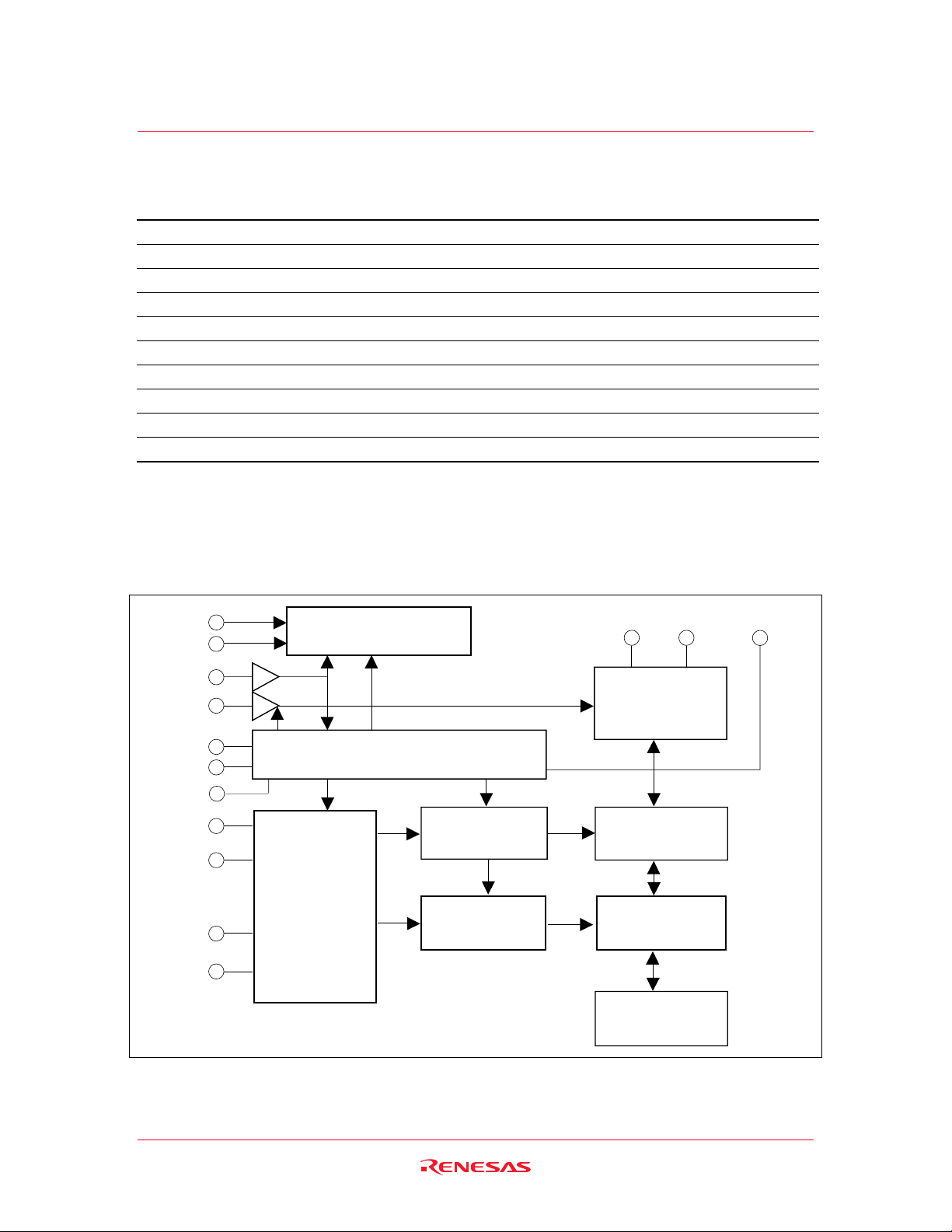
Block Diagram
Note: 1. This function is supported by only the HN58V66A series.
V
CC
V
SS
RES
OE
CE
WE
RES
A0
to
A5
A6
to
A12
1
*
1
*
High voltage generator
Control logic and timing
Address
buffer and
latch
Y decoder
X decoder
to
I/O0 I/O7
I/O buffer
and
input latch
Y gating
Memory array
Data latch
RDY/Busy
Rev.3.00, Feb.02.2004, page 4 of 26
Page 5

HN58V65AI/HN58V66AI/HN58V65A-SR/HN58V66A-SR Series
Operation Table
Operation CE OE WE RES*3 RDY/Busy I/O
Read VIL V
V
IL
V
IH
*1 High-Z Dout
H
Standby VIH ×*2 × × High-Z High-Z
Write VIL V
Deselect VIL V
Write Inhibit × × V
× V
Data Polling VIL V
Program reset × × × V
V
IH
V
IH
× ×
IL
V
IL
V
IL
V
IH
×
IH
V
IH
High-Z to VOL Din
H
High-Z High-Z
H
V
H
High-Z High-Z
IL
Dout (I/O7)
OL
Notes: 1. Refer to the recommended DC operating conditions.
2. × : Don’t care
3. This function supported by only the HN58V66A series.
Absolute Maximum Ratings
Parameter Symbol Value Unit
Power supply voltage relative to VSS VCC –0.6 to +7.0 V
Input voltage relative to VSS Vin –0.5*1 to
+7.0*3
Operating temperature range *2 HN58V65AI/HN58V66AI Topr –40 to +85 °C
HN58V65A-SR/HN58V66A-SR Topr –20 to +85 °C
Storage temperature range Tstg –55 to +125 °C
Notes: 1. Vin min : –3.0 V for pulse width ≤ 50 ns.
2. Including electr ical characteristics and data retention.
3. Should not exceed V
+ 1 V.
CC
V
Rev.3.00, Feb.02.2004, page 5 of 26
Page 6

HN58V65AI/HN58V66AI/HN58V65A-SR/HN58V66A-SR Series
Recommended DC Operating Conditions
Parameter Symbol Min Typ Max Unit
Supply voltage VCC 2.7 — 5.5 V
V
0 0 0 V
SS
Input voltage VIL –0.3*1 — 0.6*5 V
V
V
2.4*2 — VCC + 0.3*3 V
IH
*4 VCC – 0.5 — VCC + 1.0 V
H
Operating temperature Topr HN58V65AI/HN58V66AI –40 — +85 °C
HN58V65A-SR/HN58V66A-SR –20 — +85 °C
Notes: 1. VIL min: –1.0 V for pulse width ≤ 50 ns.
2. V
3. V
= 3.0 V for VCC = 3.6 to 5.5 V.
IH
max: VCC + 1.0 V for pulse width ≤ 50 ns.
IH
4. This function is supported by only the HN58V66A series.
5. V
= 0.8 V for VCC = 3.6 V to 5.5 V
IL
DC Characteristics
(Ta = −40 to +85°C, VCC = 2.7 to 5.5 V: HN58V66AI/HN58V66AI,
Ta = −20 to +85°C, V
Parameter Symbol Min Typ Max Unit Test conditions
Input leakage current ILI 2*1 µA VCC = 5.5 V, Vin = 5.5 V
Output leakage current ILO 2 µA VCC = 5.5 V, Vout = 5.5/0.4 V
Standby VCC current I
I
Operating VCC current I
10 mA Iout = 0 mA, Duty = 100%,
15 mA Iout = 0 mA, Duty = 100%,
25 mA Iout = 0 mA, Duty = 100%,
Output low voltage VOL 0.4 V IOL = 2.1 mA
Output high voltage VOH VCC × 0.8 V IOH = −400 µA
Note: 1. ILI on RES : 100 µA max (only the HN58V66A series)
1 to 2 5 µA CE = VCC
CC1
1 mA CE = VIH
CC2
6 mA Iout = 0 mA, Duty = 100%,
CC3
= 2.7 to 5.5 V: HN58V66A-SR/HN58V66A-SR)
CC
Cycle = 1 µs at V
= 3.6 V
CC
Cycle = 1 µs at VCC = 5.5 V
Cycle = 100 ns at V
= 3.6 V
CC
Cycle = 70 ns at VCC = 5.5 V
Rev.3.00, Feb.02.2004, page 6 of 26
Page 7

HN58V65AI/HN58V66AI/HN58V65A-SR/HN58V66A-SR Series
Capacitance (Ta = +25°C, f = 1 MHz)
Parameter Symbol Min Typ Max Unit Test conditions
Input capacitance Cin*1 6 pF Vin = 0 V
Output capacitance Cout*1 12 pF Vout = 0 V
Note: 1. This parameter is sampled and not 100% tested.
AC Characteristics
(Ta = −40 to +85°C, VCC = 2.7 to 5.5 V: HN58V65AI/HN58V66AI,
Ta = −20 to +85°C, V
Test Conditions
= 2.7 to 5.5 V: HN58V65A-SR/HN58V66A-SR)
CC
• Input pulse levels : 0.4 V to 2.4 V (V
0 V to V
(RES pin*2)
CC
= 2.7 to 3.6 V), 0.4 V to 3.0 V (VCC = 3.6 to 5.5 V)
CC
• Input rise and fall time : ≤ 5 ns
• Input timing reference levels : 0.8, 1.8 V
• Output load : 1TTL Gate +100 pF
• Output reference levels : 1.5 V, 1.5 V
Read Cycle 1 (2.7 ≤ V
HN58V65AI/HN58V66AI
-10
Parameter Symbol Min Max Unit Test conditions
Address to output delay t
CE to output delay tCE 100 ns OE = VIL, WE = VIH
OE to output delay tOE 10 50 ns CE = VIL, WE = VIH
Address to output hold tOH 0 ns CE = OE = VIL, WE = VIH
OE (CE) high to output float*1 tDF 0 40 ns CE = VIL, WE = VIH
RES low to output float*
RES to output delay*2 t
< 4.5 V)
CC
1, 2
t
HN58V65A-SR/HN58V66A-SR
100 ns CE = OE = VIL, WE = VIH
ACC
0 350 ns CE = OE = VIL, WE = VIH
DFR
0 450 ns CE = OE= VIL, WE = VIH
RR
Rev.3.00, Feb.02.2004, page 7 of 26
Page 8

HN58V65AI/HN58V66AI/HN58V65A-SR/HN58V66A-SR Series
Write Cycle 1 (2.7 ≤ VCC < 4.5 V)
Parameter Symbol Min*3 Typ Max Unit Test conditions
Address setup time t
Address hold time tAH 50 ns
CE to write setup time (WE controlled) tCS 0 ns
CE hold time (WE controlled) tCH 0 ns
WE to write setup time (CE controlled) tWS 0 ns
WE hold time (CE controlled) tWH 0 ns
OE to write setup time t
OE hold time t
Data setup time tDS 50 ns
Data hold time tDH 0 ns
WE pulse width (WE controlled) tWP 200 ns
CE pulse width (CE controlled) tCW 200 ns
Data latch time tDL 100 ns
Byte load cycle t
Byte load window tBL 100 µs
Write cycle time tWC 10*4 ms
Time to device busy tDB 120 ns
Write start time tDW 0*5 ns
Reset protect time*2 t
Reset high time*
Notes: 1. tDF and t
2, 6
t
are defined as the time at which the outputs achieve the open circuit conditions and
DFR
are no longer driven.
2. This function is supported by only the HN58V66A series.
3. Use this device in longer cycle than this value.
4. t
must be longer than this value unless polling techniques or RDY/Busy are used. This device
WC
automatically completes the internal write operation within this value.
5. Next read or write operation can be initiated after t
6. This parameter is sampled and not 100% tested.
7. A6 through A12 are page addresses and these addresses are latched at the first falling edge of
WE.
8. A6 through A12 are page addresses and these addresses are latched at the first falling edge of
CE.
9. See AC read characteristics.
0 ns
AS
0 ns
OES
0 ns
OEH
0.3 30 µs
BLC
100 µs
RP
1 µs
RES
if polling techniques or RDY/Busy are used.
DW
Rev.3.00, Feb.02.2004, page 8 of 26
Page 9

HN58V65AI/HN58V66AI/HN58V65A-SR/HN58V66A-SR Series
Read Cycle 2 (4.5 ≤ VCC ≤ 5.5 V)
HN58V65AI/HN58V66AI
HN58V65A-SR/HN58V66A-SR
-10
Parameter Symbol Min Max Unit Test conditions
Address to output delay t
70 ns CE = OE = VIL, WE = VIH
ACC
CE to output delay tCE 70 ns OE = VIL, WE = VIH
OE to output delay tOE 10 40 ns CE = VIL, WE = VIH
Address to output hold tOH 0 ns CE = OE = VIL, WE = VIH
OE (CE) high to output float*1 tDF 0 30 ns CE = VIL, WE = VIH
RES low to output float*
RES to output delay*2 t
1, 2
t
0 350 ns CE = OE = VIL, WE = VIH
DFR
0 450 ns CE = OE= VIL, WE = VIH
RR
Rev.3.00, Feb.02.2004, page 9 of 26
Page 10

HN58V65AI/HN58V66AI/HN58V65A-SR/HN58V66A-SR Series
Write Cycle 2 (4.5 ≤ VCC ≤ 5.5 V)
Parameter Symbol Min*3 Typ Max Unit Test conditions
Address setup time t
Address hold time tAH 50 ns
CE to write setup time (WE controlled) tCS 0 ns
CE hold time (WE controlled) tCH 0 ns
WE to write setup time (CE controlled) tWS 0 ns
WE hold time (CE controlled) tWH 0 ns
OE to write setup time t
OE hold time t
Data setup time tDS 50 ns
Data hold time tDH 0 ns
WE pulse width (WE controlled) tWP 100 ns
CE pulse width (CE controlled) tCW 100 ns
Data latch time tDL 50 ns
Byte load cycle t
Byte load window tBL 100 µs
Write cycle time tWC 10*4 ms
Time to device busy tDB 120 ns
Write start time tDW 0*5 ns
Reset protect time*2 t
Reset high time*
Notes: 1. tDF and t
2, 6
t
are defined as the time at which the outputs achieve the open circuit conditions and
DFR
are no longer driven.
2. This function is supported by only the HN58V66A.
3. Use this device in longer cycle than this value.
4. t
must be longer than this value unless polling techniques or RDY/Busy are used. This device
WC
automatically completes the internal write operation within this value.
5. Next read or write operation can be initiated after t
6. This parameter is sampled and not 100% tested.
7. A6 through A12 are page address and these addresses are latched at the first falling edge of
WE.
8. A6 through A12 are page address and these addresses are latched at the first falling edge of CE.
9. See AC read characteristics.
0 ns
AS
0 ns
OES
0 ns
OEH
0.2 30 µs
BLC
100 µs
RP
1 µs
RES
if polling techniques or RDY/Busy are used.
DW
Rev.3.00, Feb.02.2004, page 10 of 26
Page 11
HN58V65AI/HN58V66AI/HN58V65A-SR/HN58V66A-SR Series
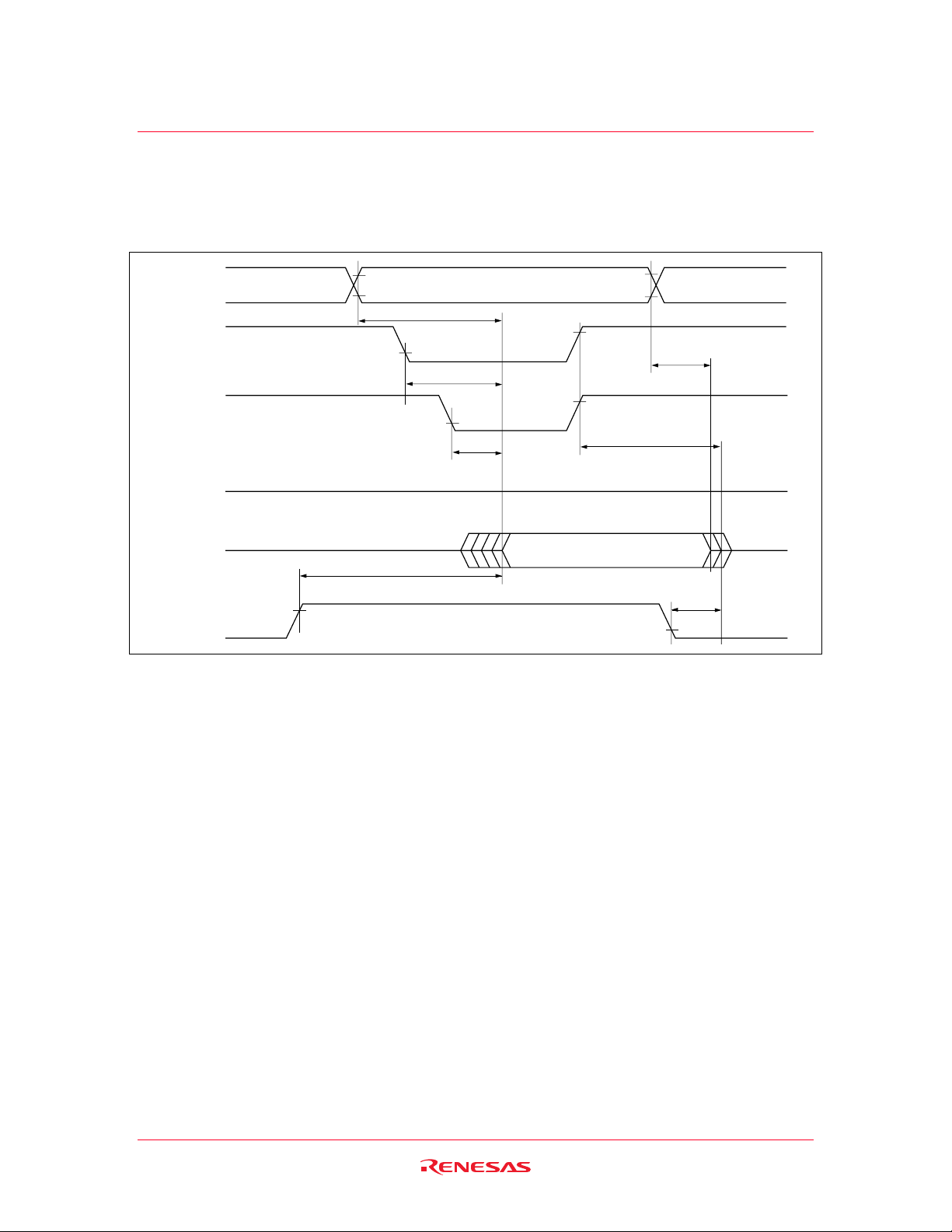
Timing Waveforms
Read Timing Waveform
Address
t
ACC
CE
OE
WE
Data Out
2
RES *
High
t
t
CE
t
OE
OH
t
DF
Data out valid
t
RR
t
DFR
Rev.3.00, Feb.02.2004, page 11 of 26
Page 12

HN58V65AI/HN58V66AI/HN58V65A-SR/HN58V66A-SR Series
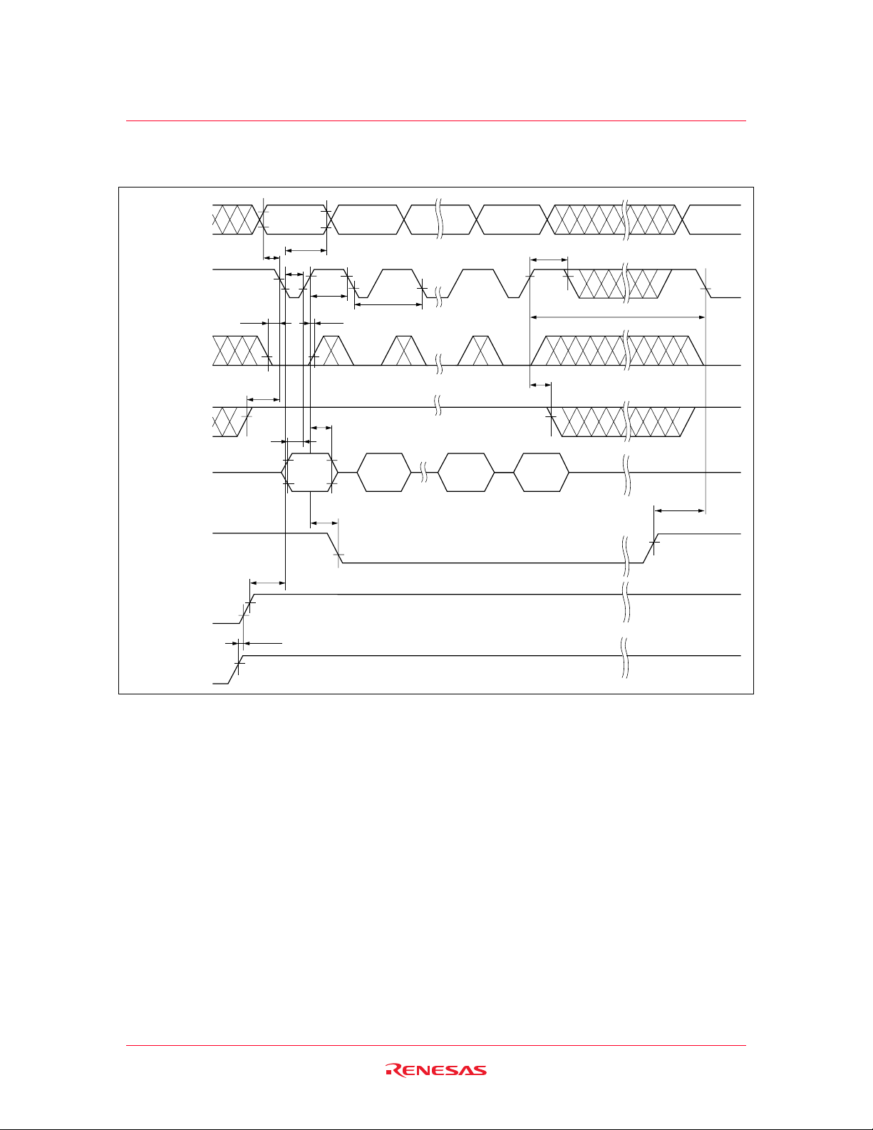
Byte Write Timing Waveform(1) (WE Controlled)
Address
t
t
AH
CS
CE
t
CH
t
WC
WE
OE
Din
RDY/Busy
RES *
V
CC
t
AS
t
OES
t
WP
t
DS
High-Z
t
RP
t
RES
2
t
BL
t
OEH
t
DH
t
DW
t
DB
High-Z
Rev.3.00, Feb.02.2004, page 12 of 26
Page 13

HN58V65AI/HN58V66AI/HN58V65A-SR/HN58V66A-SR Series
Byte Write Timing Waveform(2) (CE Controlled)
Address
t
CE
WE
OE
t
t
AS
t
OES
WS
AH
t
CW
t
t
OEH
t
BL
WH
t
WC
Din
RDY/Busy
2
RES *
V
CC
t
DS
High-Z High-Z
t
RP
t
RES
t
t
DH
DB
t
DW
Rev.3.00, Feb.02.2004, page 13 of 26
Page 14

HN58V65AI/HN58V66AI/HN58V65A-SR/HN58V66A-SR Series
Page Write Timing Waveform(1) (WE Controlled)
Address
A0 to A12
WE
CE
OE
Din
RDY/Busy
*7
t
t
AH
AS
t
WP
t
DL
t
CS
t
OES
t
DS
High-Z High-Z
t
RP
t
CH
t
DH
t
DB
t
BLC
t
OEH
t
BL
t
WC
t
DW
RES *
V
CC
2
t
RES
Rev.3.00, Feb.02.2004, page 14 of 26
Page 15
HN58V65AI/HN58V66AI/HN58V65A-SR/HN58V66A-SR Series
Page Write Timing Waveform(2) (CE Controlled)
Address
A0 to A12
CE
WE
OE
Din
RDY/Busy
*8
t
AH
t
AS
t
CW
t
DL
t
WS
t
OES
t
DS
High-Z High-Z
t
RP
t
WH
t
DH
t
DB
t
BLC
t
OEH
t
BL
t
WC
t
DW
RES *
V
CC
2
t
RES
Rev.3.00, Feb.02.2004, page 15 of 26
Page 16
HN58V65AI/HN58V66AI/HN58V65A-SR/HN58V66A-SR Series
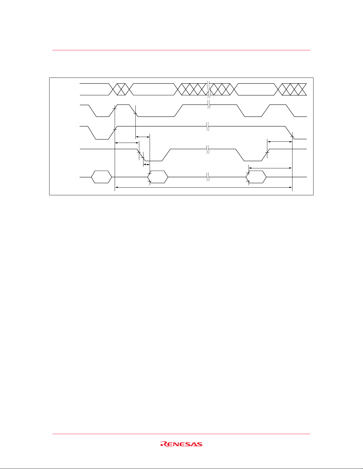
Data Polling Timing Waveform
Address
CE
WE
OE
I/O7
OE
An
*9
t
CE
*9
Dout X
t
WC
Dout X
An An
t
OEH
t
Din X
t
DW
t
OES
Rev.3.00, Feb.02.2004, page 16 of 26
Page 17
HN58V65AI/HN58V66AI/HN58V65A-SR/HN58V66A-SR Series
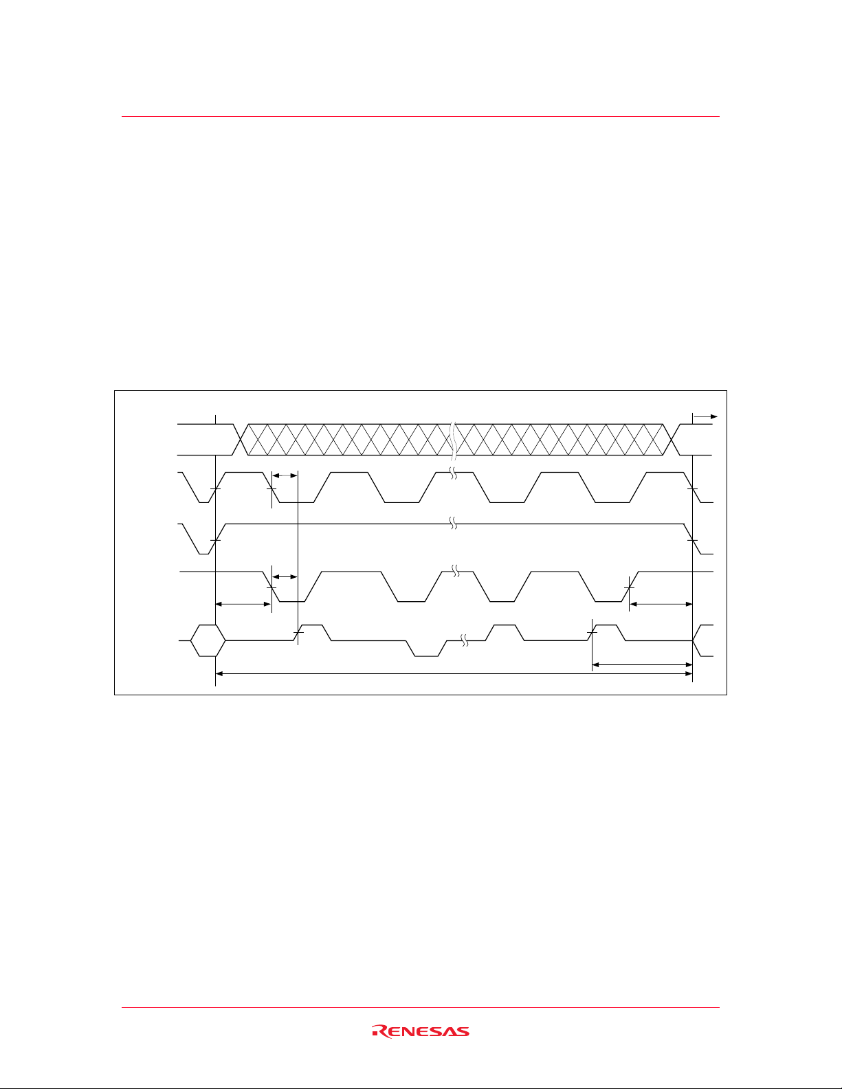
Toggle Bit
This device provide another function to determine the internal programming cycle. If the EEPROM is set to
read mode during the internal programming cycle, I/O6 will charge from “1” to “0” (toggling) for each
read. When the internal programming cycle is finished, toggling of I/O6 will stop and the device can be
accessible for next read or program.
Toggle Bit Waveform
Notes: 1. I/O6 beginning state is “1”.
2. I/O6 ending state will vary.
3. See AC read characteristics.
4. Any address location can be used, but the address must be fixed.
Next mode
*4
Address
*3
t
CE
CE
WE
OE
I/O6
Din
t
OEH
*3
t
OE
*1 *2 *2
Dout
Dout Dout Dout
t
WC
t
DW
t
OES
Rev.3.00, Feb.02.2004, page 17 of 26
Page 18

HN58V65AI/HN58V66AI/HN58V65A-SR/HN58V66A-SR Series
Software Data Protection Timing Waveform(1) (in protec t i on m ode)
V
CC
CE
WE
t
BLC
t
WC
Address
Data
1555
AA
0AAA
55
1555
A0
Write address
Write data
Software Data Protection Timing Waveform(2) (in non-p rot ect i on mode)
V
CC
CE
WE
Address
Data
1555AA0AAA551555801555AA0AAA551555
20
t
WC
Normal active
mode
Rev.3.00, Feb.02.2004, page 18 of 26
Page 19

HN58V65AI/HN58V66AI/HN58V65A-SR/HN58V66A-SR Series
Functional Description
Automatic Page Write
Page-mode write feature allows 1 to 64 bytes of data to be written into the EEPROM in a single write
cycle. Following the initial byte cycle, an additional 1 to 63 bytes can be written in the same manner. Each
additional byte load cycle must be started within 30 µs from the preceding falling edge of WE or CE. Whe n
CE or WE is kept high for 100 µs after data input, the EEPROM enters write mode automatically and the
input data are written into the EEPROM.
Data Polling
Data polling indicates the status that the EEPROM is in a write cycle or not. If EEPROM is set to read
mode during a write cycle, an inversion of the last byte of data outputs from I/O7 to indicate that the
EEPROM is performing a write operation.
RDY/Busy Signal
RDY/Busy signal also allows status of the EEPROM to be determined. The RDY/Busy signal has high
impedance except in write cycle and is lowered to V
cycle, the RDY/Busy signal changes state to high impedance.
after the first write signal. At the end of a write
OL
RES Signal (only the HN58V66A series)
When RES is low, the EEPROM cannot be read or programmed. Therefore, data can be protected by
keeping RES low when V
is switched. RES should be high during read and programming because it
CC
doesn’t provide a latch function.
V
CC
RES
Read inhibit Read inhibit
Program inhibit
Program inhibit
Rev.3.00, Feb.02.2004, page 19 of 26
Page 20

HN58V65AI/HN58V66AI/HN58V65A-SR/HN58V66A-SR Series
WE, CE Pin Operation
During a write cycle, addresses are latched by the falling edge of WE or CE, and data is latched by the
rising edge of WE or CE.
Write/Erase Endurance and Data Retention Time
The endurance is 10
5
cycles in case of the page programming and 104 cycles in case of the byte
programming (1% cumulative failure rate). The data retention time is more than 10 years when a device is
page-programmed less than 10
4
cycles.
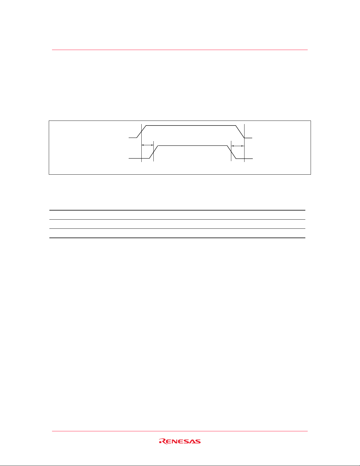
Data Protection
To prevent this phenomenon, this device has a noise cancellation function that cuts noise if its width is 15
ns or less.
1. Data Protection against Noise on Control Pins (CE, OE, WE) during Operation
During readout or standby, noise on the control pins may act as a trigger and turn the EEPROM to
programming mode by mistake. Be careful not to allow noise of a width of more than 15 ns on the
control pins.
WE
CE
OE
V
0 V
V
0 V
IH
IH
Rev.3.00, Feb.02.2004, page 20 of 26
15 ns max
Page 21
HN58V65AI/HN58V66AI/HN58V65A-SR/HN58V66A-SR Series
2. Data protection at VCC on/off
When V
is turned on or off, noise on the control pins generated by external circuits (CPU, etc) may
CC
act as a trigger and turn the EEPROM to program mode by mistake. To prevent this unintentional
programming, the EEPROM must be kept in an unprogrammable state while the CPU is in an unstable
state.
Note: The EEPROM should be kept in unprogrammable state during VCC on/off by using CPU RESET
signal.
V
CC
CPU
RESET
*
Unprogrammable
*
Unprogrammable
2.1 Protection by CE, OE, WE
To realize the unprogrammable state, the input level of control pins must be held as shown in the
table below.
CE VCC × ×
OE × V
WE × × V
×: Don’t care.
VCC: Pull-up to VCC level.
: Pull-down to VSS level.
V
SS
×
SS
CC
Rev.3.00, Feb.02.2004, page 21 of 26
Page 22

HN58V65AI/HN58V66AI/HN58V65A-SR/HN58V66A-SR Series
2.2 Protection by RES (only the HN 5 8V 6 6A series)
The unprogrammable state can be realized by that the CPU’s reset signal inputs directly to the
EEPROM’s RES pin. RES should be kept V
level during VCC on/off. The EEPROM breaks off
SS
programming operation when RES becomes low, programming operation doesn’t finish correctly
in case that RES falls low during programming operation. RES should be kept high for 10 ms after
the last data input.
V
CC
RES
Program inhibit
WE
or CE
1 µs min
100 µs min
10 ms min
Program inhibit
Rev.3.00, Feb.02.2004, page 22 of 26
Page 23

HN58V65AI/HN58V66AI/HN58V65A-SR/HN58V66A-SR Series
3. Software data protection
To prevent unintentional programming caused by noise generated by external circuits, this device has
the software data protection function. In software data protection mode, 3 bytes of data must be input
before write data as follows. And these bytes can switch the non-protection mode to the protection
mode. SDP is enabled if only the 3 byte code is input.
Address
1555
↓
0AAA
↓
1555
↓
Write address Normal data input
Data
AA
↓
55
↓
A0
↓
Write data }
Software data protection mode can be canceled by inputting the following 6 bytes. After that, this device
turns to the non-protection mode and can write data normally. But when the data is input in the canceling
cycle, the data cannot be written.
Address
1555
↓
0AAA
↓
1555
↓
1555
↓
0AAA
↓
1555
Data
AA
↓
55
↓
80
↓
AA
↓
55
↓
20
The software data protection is not enabled at the shipment.
Note: There are some differences between Renesas Technology’s and other company’s for enable/disable
sequence of software data protection. If there are any questions, please contact with Renesas
Technology’s sales offices.
Rev.3.00, Feb.02.2004, page 23 of 26
Page 24

HN58V65AI/HN58V66AI/HN58V65A-SR/HN58V66A-SR Series
Package Dimensions
HN58V65API Series
HN58V66API Series (DP-28, DP-28V)
28
1
1.9 Max
2.54 ± 0.25
1.2
35.6
36.5 Max
0.48 ± 0.10
15
14
0.51 Min
Package Code
JEDEC
JEITA
Mass
13.4
14.6 Max
5.70 Max
2.54 Min
0
˚ – 15˚
(reference value)
15.24
+ 0.11
0.25
– 0.05
DP-28, DP-28V
—
Conforms
4.6 g
Unit: mm
Rev.3.00, Feb.02.2004, page 24 of 26
Page 25

HN58V65AI/HN58V66AI/HN58V65A-SR/HN58V66A-SR Series
Package Dimensions (cont)
HN58V65AFPI Series
HN58V66AFPI Series (FP-28D, FP-28DV)
18.3
18.8 Max
Unit: mm
28
1
1.12 Max
1.27
*0.40 ± 0.08
0.38 ± 0.06
*Dimension including the plating thickness
Base material dimension
0.15
0.20
15
14
M
8.4
2.50 Max
0.20 ± 0.10
0.15 ± 0.04
*0.17 ± 0.05
Package Code
JEDEC
JEITA
Mass
(reference value)
11.8 ± 0.3
1.7
1.0 ± 0.2
0˚ – 8˚
FP-28D, FP-28DV
Conforms
—
0.7 g
Rev.3.00, Feb.02.2004, page 25 of 26
Page 26

HN58V65AI/HN58V66AI/HN58V65A-SR/HN58V66A-SR Series
Package Dimensions (cont)
HN58V65ATI Series
HN58V66ATI Series
HN58V65AT-SR Series
HN58V66AT-SR Series (TFP-28DB, TFP-28DBV)
8.00
8.20 Max
28
15
11.80
Unit: mm
1
14
0.55
*0.22 ± 0.08
0.20 ± 0.06
0.10
M
0.45 Max
0.10
1.20 Max
*Dimension including the plating thickness
Base material dimension
13.40 ± 0.30
+0.07
–0.08
0.13
0.15 ± 0.04
*0.17 ± 0.05
0.80
0˚ – 5˚
0.50 ± 0.10
Package Code
JEDEC
JEITA
Mass
(reference value)
TFP-28DB, TFP-28DBV
—
—
0.23 g
Rev.3.00, Feb.02.2004, page 26 of 26
Page 27

Revision History
HN58V65AI/HN58V66AI/HN58V65A-SR/HN58V66A-SR Series Data Sheet
Contents of Modification Rev. Date
Page Description
0.0 Mar. 12, 1997 Initial issue
1.0 Aug. 29, 1997
7
11
19
2.0 Oct. 31, 1997 6 DC Characteristics
3.00 Feb. 02, 2004 2
24-26
Addition of HN58V65A-SR/HN58V66A-SR
AC Characteristics
Input pulse level: 0.4 V to VCC to 0 V to VCC
Timing Waveform
Read Timing Waveform: Correct error
Functional Description
Data Protection 3.: Addition of description
I
Ordering Information
Addition of HN58V65API-10E, HN58V66API-10E,
HN58V65AFPI-10E, HN58V66AFPI-10E,
HN58V65ATI-10E, HN58V66ATI-10E, HN58V65AT-10SRE,
HN58V66AT-10SRE
Package Dimensions
DP-28 to DP-28, DP-28V
FP-28D to FP-28D, FP-28DV
TFP-28DB to TFP-28DB, TFP-28DBV
(max): 6/10/12/25 mA to 6/10/15/25 mA
CC3
Page 28

©
.
!
y
may
.
gy
.
7
b
y
.
.
S
ales Strategic Planning Div. Nippon Bldg., 2-6-2, Ohte-machi, Chiyoda-ku, Tokyo 100-0004, Japa
n
m
Keep safety first in your circuit designs
1. Renesas Technology Corp. puts the maximum effort into making semiconductor products better and more reliable, but there is alwa
occur with them. Trouble with semiconductors may lead to personal injury, fire or property damage
Remember to give due consideration to safety when making your circuit designs, with appropriate measures such as (i) placement of substitutive, auxiliary
circuits, (ii) use of nonflammable material or (iii) prevention against any malfunction or mishap.
Notes regarding these materials
1. These materials are intended as a reference to assist our customers in the selection of the Renesas Technology Corp. product best suited to the customer's
application; they do not convey any license under any intellectual property rights, or any other rights, belonging to Renesas Technology Corp. or a third party.
2. Renesas Technology Corp. assumes no responsibility for any damage, or infringement of any third-party's rights, originating in the use of any product data,
diagrams, charts, programs, algorithms, or circuit application examples contained in these materials.
3. All information contained in these materials, including product data, diagrams, charts, programs and algorithms represents information on products at the time of
publication of these materials, and are subject to change by Renesas Technology Corp. without notice due to product improvements or other reasons. It is
therefore recommended that customers contact Renesas Technology Corp. or an authorized Renesas Technology Corp. product distributor for the latest product
information before purchasing a product listed herein.
The information described here may contain technical inaccuracies or typographical errors.
Renesas Technology Corp. assumes no responsibility for any damage, liability, or other loss rising from these inaccuracies or errors.
Please also pay attention to information published by Renesas Technology Corp. by various means, including the Renesas Technology Corp. Semiconductor
home page (http://www.renesas.com).
4. When using any or all of the information contained in these materials, including product data, diagrams, charts, programs, and algorithms, please be sure to
evaluate all information as a total system before making a final decision on the applicability of the information and products. Renesas Technology Corp. assumes
no responsibility for any damage, liability or other loss resulting from the information contained herein.
5. Renesas Technology Corp. semiconductors are not designed or manufactured for use in a device or system that is used under circumstances in which human life
is potentially at stake. Please contact Renesas Technology Corp. or an authorized Renesas Technology Corp. product distributor when considering the use of a
product contained herein for any specific purposes, such as apparatus or systems for transportation, vehicular, medical, aerospace, nuclear, or undersea repeater
use.
6. The prior written approval of Renesas Technolo
. If these products or technologies are subject to the Japanese export control restrictions, they must be exported under a license from the Japanese government and
cannot
An
8. Please contact Renesas Technology Corp. for further details on these materials or the products contained therein
e imported into a country other than the approved destination.
diversion or reexport contrary to the export control laws and regulations of Japan and/or the country of destination is prohibited
Corp. is necessary to reprint or reproduce in whole or in part these materials
s the possibility that trouble
RENESAS SALES OFFICES
Renesas Technology America, Inc.
450 Holger Way, San Jose, CA 95134-1368, U.S.A
Tel: <1> (408) 382-7500 Fax: <1> (408) 382-7501
Renesas Technology Europe Limited.
Dukes Meadow, Millboard Road, Bourne End, Buckinghamshire, SL8 5FH, United Kingdom
Tel: <44> (1628) 585 100, Fax: <44> (1628) 585 900
Renesas Technology Europe GmbH
Dornacher Str. 3, D-85622 Feldkirchen, Germany
Tel: <49> (89) 380 70 0, Fax: <49> (89) 929 30 11
Renesas Technology Hong Kong Ltd.
7/F., North Tower, World Finance Centre, Harbour City, Canton Road, Hong Kong
Tel: <852> 2265-6688, Fax: <852> 2375-6836
Renesas Technology Taiwan Co., Ltd.
FL 10, #99, Fu-Hsing N. Rd., Taipei, Taiwan
Tel: <886> (2) 2715-2888, Fax: <886> (2) 2713-2999
Renesas Technology (Shanghai) Co., Ltd.
26/F., Ruijin Building, No.205 Maoming Road (S), Shanghai 200020, China
Tel: <86> (21) 6472-1001, Fax: <86> (21) 6415-2952
Renesas Technology Singapore Pte. Ltd.
1, Harbour Front Avenue, #06-10, Keppel Bay Tower, Singapore 098632
Tel: <65> 6213-0200, Fax: <65> 6278-8001
2003. Renesas Technology Corp., All rights reserved. Printed in Japan
http://www.renesas.co
Colophon 1.0
 Loading...