

Page 1
HD74HC1G66
Analog Switch
REJ03D0188–0800Z
(Previous ADE-205-314F (Z))
Rev.8.00
Jan.27.2004
Description
The HD74HC1G66 is high-speed CMOS analog switch using silicon gate CMOS process. With CMOS
low power dissipation, it provides high speed. The device has low ON resistance for good transfer
characteristics and can take wide range of input voltage.
Features
• The basic gate function is lined up as Renesas uni logic series.
• Supplied on emboss taping for high-speed automatic mounting.
• Electrical characteristics equivalent to the HD74HC4066
Supply voltage range : 2 to 6 V
Operating temperature range : –40 to +85°C
• Ordering Information
Part Name Package Type Package Code Package
Abbreviation
HD74HC1G66CME CMPAK-5 pin CMPAK-5A CM E (3,000 pcs/reel)
Taping Abbreviation
(Quantity)
Rev.8.00, Jan.27.2004, page 1 of 8
Page 2
HD74HC1G66
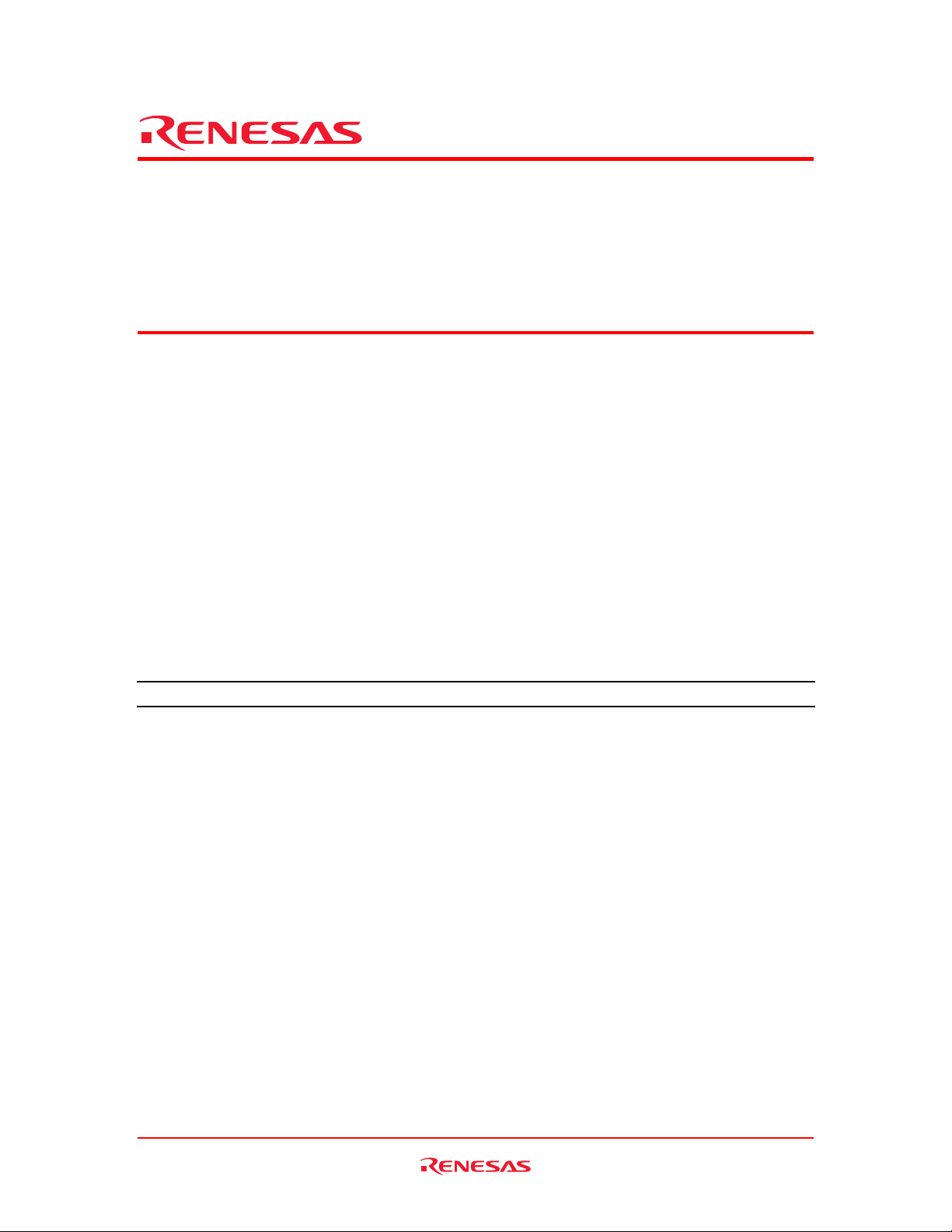
Outline and Article Indication
• HD74HC1G66
Index band
Marking
H 9
CMPAK-5
Function Table
Control Switch
LOFF
HON
H : High level
L : Low level
GND ≤ V
GND ≤ V
IN
OUT
≤ V
≤ V
CC
CC
= Control code
Pin Arrangement
IN/OUT
OUT/IN
GND
Rev.8.00, Jan.27.2004, page 2 of 8
1
2
3
(Top view)
54V
CC
Control
Page 3
HD74HC1G66
Absolute Maximum Ratings
Item Symbol Ratings Unit Test Conditions
Supply voltage range V
Input voltage range *
Output voltage range *
1
1, 2
Input clamp current I
Output clamp current I
Continuous output current I
Continuous current through
or GND
V
CC
Maximum power dissipation
at Ta = 25°C (in still air) *
3
CC
V
I
V
O
IK
OK
O
I
or I
CC
GND
P
T
Storage temperature Tstg –65 to 150 °C
Notes: The absolute maximum ratings are values, which must not individually be exceeded, and
furthermore, no two of which may be realized at the same time.
1. The input and output voltage ratings may be exceeded if the input and output clamp-current
ratings are observed.
2. This value is limited to 5.5 V maximum.
3. The maximum package power dissipation was calculated using a junction temperature of 150°C.
–0.5 to 7.0 V
–0.5 to VCC + 0.5 V
–0.5 to VCC + 0.5 V Output : H or L
±20 mA VI < 0 or VI > V
±20 mA VO < 0 or VO >V
±25 mA VO = 0 to V
CC
±25 mA
200 mW
CC
CC
Recommended Operating Conditions
Item Symbol Min Max Unit Test Conditions
Supply voltage range V
Input voltage range V
Output voltage range V
Input rise / fall time
tr, t
CC
I/O
O
f
(Control input 10% to 90%)
Operating temperature Ta –40 85 °C
Note: Unused or floating control inputs must be held high or low.
26V
0VCCV
0VCCV
0 1000 VCC = 2.0 V
ns
0 500 VCC = 4.5 V
0 400
VCC = 6.0 V
Rev.8.00, Jan.27.2004, page 3 of 8
Page 4
HD74HC1G66
Electrical Characteristics
V
CC
Item Symbo
Input voltage
On resistance R
Peak on
V
IH
V
IL
ON
RON (p)
resistance
I
Leak current
Input current I
Operating
(off) 6.0 — — ±0.1 — ±1.0 µAV
S
I
(on) 6.0 — — ±0.1 — ±1.0 µAV
S
IN
I
CC
current
(V)
2.0 1.5 — — 1.5 —
4.5 3.15 — — 3.15 —
6.0 4.2 — — 4.2 —
2.0 — — 0.5 — 0.5
4.5 — — 1.35 — 1.35
6.0 — — 1.8 — 1.8
2.0 — 200 450 — 550
4.5 — 90 160 — 180
6.0 — 80 130 — 140
2.0 — 600 1500 — 2000
4.5 — 125 200 — 250
6.0 — 100 170 — 210
6.0 — — ±0.1 — ±1.0 µAV
6.0 — — 1.0 — 10.0 µAV
Ta = 25°C Ta = –40 to 85°C
Min Typ Max Min Max
Unit Test Conditions
V Control input only
Ω V
C
= V
IH
VIN = VCC or GND
IT = 1 mA
Ω V
= V
C
IH
VIN = 0 to V
I
= 1 mA
IN/OUT
= V
C
IL
VIN = VCC, V
CC
OUT
= GND
or VIN = GND,
V
= V
OUT
CC
= V
C
IH
VIN = VCC or GND
= VCC or GND
IN
= VCC or GND
IN
Rev.8.00, Jan.27.2004, page 4 of 8
Page 5
HD74HC1G66
Switching Characteristics
Item Symbol
Propagation delay time t
Output enable time tZH, t
Output disable time tHZ, t
Maximum control
frequency
Control input
capacitance
Switch I/O capacitance C
Feed through
capacitance
Power dissipation
capacitance
(CL = 50 pF, tr = tf = 6 ns)
PLH
t
PHL
C
IN
IN/OUT
C
IN–OUT
C
PD
,
ZL
LZ
V
Ta = 25°C Ta = –40 to 85°C
CC
(V)
Min Typ Max Min Max
2.0 — — 50 — 65
4.5 — 4 10 — 13
6.0 — — 9 — 11
2.0 — — 115 — 145
4.5 — 10 23 — 29
6.0 — — 20 — 25
2.0 — — 115 — 145
4.5 — 14 23 — 29
6.0 — — 20 — 25
2.0 — 20 — — —
4.5 — 30 — — —
6.0 — 30 — — —
—2.55 — 5 pF
—2.5—— — pF
—0.5—— — pF
—5 —— — pF
Unit Test Conditions
ns R
ns R
ns R
= 10 kΩ
L
= 1 kΩ
L
= 1 kΩ
L
MHz
Rev.8.00, Jan.27.2004, page 5 of 8
Page 6
HD74HC1G66
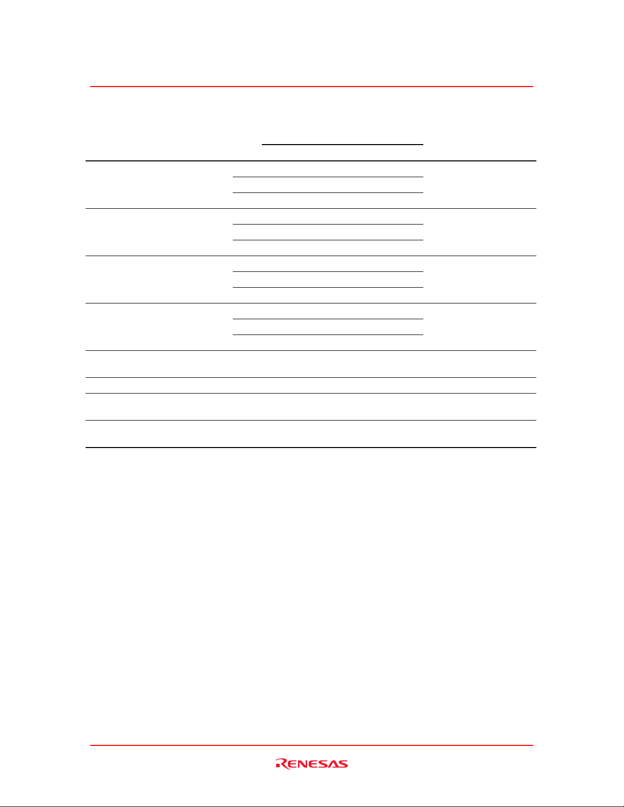
Test Circuit
• R
ON
VIN = V
CC
V
CC
= V
V
C
IH
V
(ON)
CC
GND
V
OUT
RON =
V
IN-OUT
10
(Ω)
–3
• IS (off), IS (on)
VC = V
IL
A
CC
PHL
IH
•
t
VIN = V
or GND
PLH
= V
V
C
V
IN
, t
+–
V
CC
1.0 mA
V
V
IN-OUT
VC = V
V
CC
(OFF)
V
= GND
GND
V
CC
OUT
or V
CC
= V
V
IN
or GND
A
CC
tr = 6 ns tf = 6 ns
V
V
(ON)
GND
CC
RL =
10 kΩ
CL =
50 pF
V
OUT
V
IN
OUT
50% 50%
t
PLH
IL
90% 90%
50% 50%
(ON)
V
CC
V
CC
GND
10%10%
t
PHL
V
OUT
OPEN
V
CC
GND
V
OH
V
OL
Rev.8.00, Jan.27.2004, page 6 of 8
Page 7
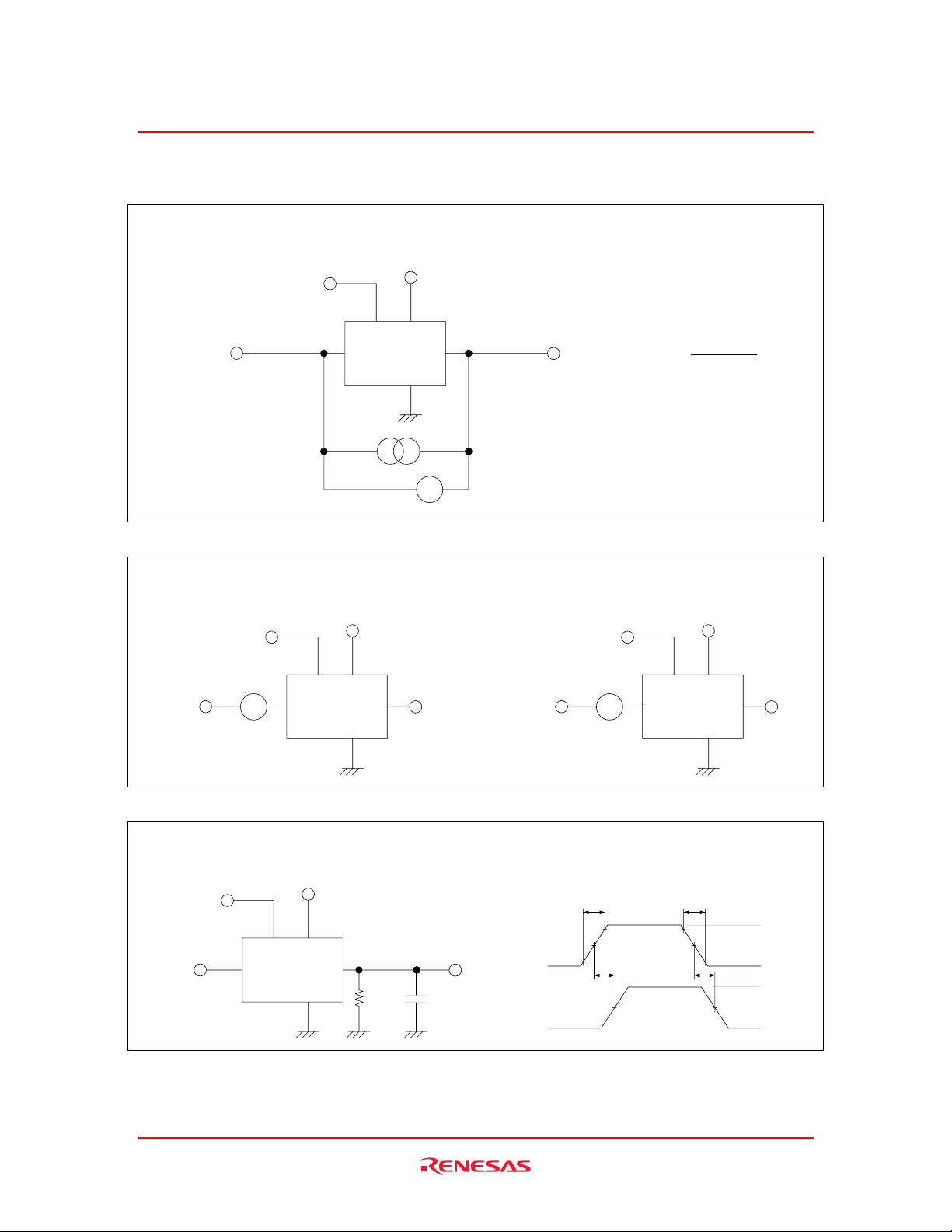
HD74HC1G66
•
tZH, tZL / tHZ, t
LZ
V
CC
V
C
R
1 kΩ
V
CC
V
S1 S2
IN
GND
V
OUT
CL =
50 pF
R
1 kΩ
Item S1 S2
t
ZH
t
ZL
t
HZ
t
LZ
V
CC
GND
V
CC
GND
GND
V
CC
GND
V
CC
=
L
=
L
Waveform - A
Waveform - B
tr = 6 ns tf = 6 ns
V
C
90% 90%
50% 50%
t
ZH
50%
V
OUT
t
ZL
50%
Notes: 1. Waveform - A is for an output with internal conditions such that the output is high
except when disabled by the output control.
2. Waveform - B is for an output with internal conditions such that the output is low
except when disabled by the output control.
• Maximum control frequency
V
CC
V
C
V
CC
V
= V
V
IN
CC
GND
OUT
RL =
1 kΩ
CL =
15 pF
V
C
V
OUT
t
LZ
10%10%
t
HZ
90%
10%
VCC/2
V
CC
GND
V
CC
GND
V
OH
GND
V
CC
V
OL
• C
IN/OUT
, C
IN-OUT
C
IN/OUT
Rev.8.00, Jan.27.2004, page 7 of 8
V
C
= GND
C
IN-OUT
V
V
(OFF)
GND
CC
CC
C
IN/OUT
Page 8

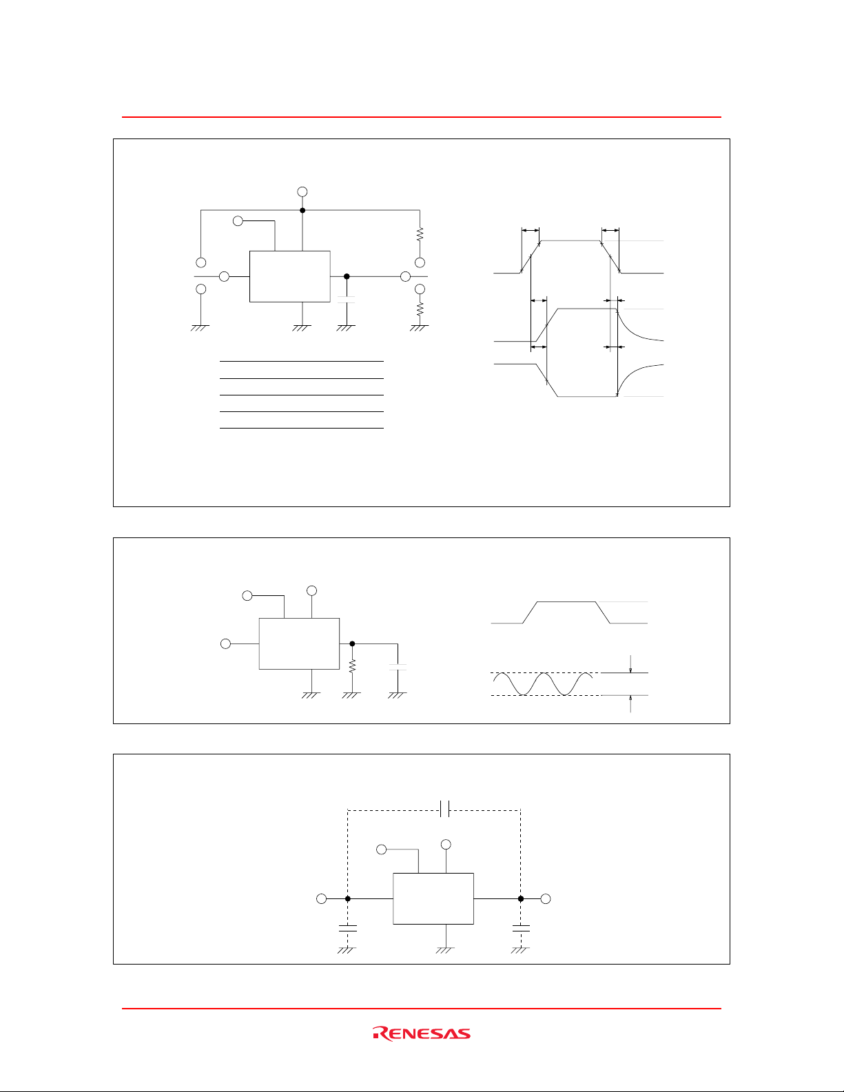
HD74HC1G66
Package Dimensions
(0.65)
5 – 0.2 ± 0.05
1.3 ± 0.2
2.0 ± 0.2
(0.65)
(0.2)
(0.425)(0.425) 1.25 ± 0.1
2.1 ± 0.3
0.9 ± 0.1
+ 0.1
0.15
– 0.05
0 – 0.1
Unit: mm
Package Code
JEDEC
JEITA
(reference value)
Mass
CMPAK–5V
—
Conforms
0.006 g
Rev.8.00, Jan.27.2004, page 8 of 8
Page 9

Sales Strategic Planning Div. Nippon Bldg., 2-6-2, Ohte-machi, Chiyoda-ku, Tokyo 100-0004, Japan
m
C
.0
Keep safety first in your circuit designs!
1. Renesas Technology Corp. puts the maximum effort into making semiconductor products better and more reliable, but there is always the possibility that trouble
may occur with them. Trouble with semiconductors may lead to personal injury, fire or property damage.
Remember to give due consideration to safety when making your circuit designs, with appropriate measures such as (i) placement of substitutive, auxiliary
circuits, (ii) use of nonflammable material or (iii) prevention against any malfunction or mishap.
Notes regarding these materials
1. These materials are intended as a reference to assist our customers in the selection of the Renesas Technology Corp. product best suited to the customer's
application; they do not convey any license under any intellectual property rights, or any other rights, belonging to Renesas Technology Corp. or a third party.
2. Renesas Technology Corp. assumes no responsibility for any damage, or infringement of any third-party's rights, originating in the use of any product data,
diagrams, charts, programs, algorithms, or circuit application examples contained in these materials.
3. All information contained in these materials, including product data, diagrams, charts, programs and algorithms represents information on products at the time of
publication of these materials, and are subject to change by Renesas Technology Corp. without notice due to product improvements or other reasons. It is
therefore recommended that customers contact Renesas Technology Corp. or an authorized Renesas Technology Corp. product distributor for the latest product
information before purchasing a product listed herein.
The information described here may contain technical inaccuracies or typographical errors.
Renesas Technology Corp. assumes no responsibility for any damage, liability, or other loss rising from these inaccuracies or errors.
Please also pay attention to information published by Renesas Technology Corp. by various means, including the Renesas Technology Corp. Semiconductor
home page (http://www.renesas.com).
4. When using any or all of the information contained in these materials, including product data, diagrams, charts, programs, and algorithms, please be sure to
evaluate all information as a total system before making a final decision on the applicability of the information and products. Renesas Technology Corp. assumes
no responsibility for any damage, liability or other loss resulting from the information contained herein.
5. Renesas Technology Corp. semiconductors are not designed or manufactured for use in a device or system that is used under circumstances in which human life
is potentially at stake. Please contact Renesas Technology Corp. or an authorized Renesas Technology Corp. product distributor when considering the use of a
product contained herein for any specific purposes, such as apparatus or systems for transportation, vehicular, medical, aerospace, nuclear, or undersea repeater
use.
6. The prior written approval of Renesas Technology Corp. is necessary to reprint or reproduce in whole or in part these materials.
7. If these products or technologies are subject to the Japanese export control restrictions, they must be exported under a license from the Japanese government and
cannot be imported into a country other than the approved destination.
Any diversion or reexport contrary to the export control laws and regulations of Japan and/or the country of destination is prohibited.
8. Please contact Renesas Technology Corp. for further details on these materials or the products contained therein.
RENESAS SALES OFFICES
Renesas Technology America, Inc.
450 Holger Way, San Jose, CA 95134-1368, U.S.A
Tel: <1> (408) 382-7500 Fax: <1> (408) 382-7501
Renesas Technology Europe Limited.
Dukes Meadow, Millboard Road, Bourne End, Buckinghamshire, SL8 5FH, United Kingdom
Tel: <44> (1628) 585 100, Fax: <44> (1628) 585 900
Renesas Technology Europe GmbH
Dornacher Str. 3, D-85622 Feldkirchen, Germany
Tel: <49> (89) 380 70 0, Fax: <49> (89) 929 30 11
Renesas Technology Hong Kong Ltd.
7/F., North Tower, World Finance Centre, Harbour City, Canton Road, Hong Kong
Tel: <852> 2265-6688, Fax: <852> 2375-6836
Renesas Technology Taiwan Co., Ltd.
FL 10, #99, Fu-Hsing N. Rd., Taipei, Taiwan
Tel: <886> (2) 2715-2888, Fax: <886> (2) 2713-2999
Renesas Technology (Shanghai) Co., Ltd.
26/F., Ruijin Building, No.205 Maoming Road (S), Shanghai 200020, China
Tel: <86> (21) 6472-1001, Fax: <86> (21) 6415-2952
Renesas Technology Singapore Pte. Ltd.
1, Harbour Front Avenue, #06-10, Keppel Bay Tower, Singapore 098632
Tel: <65> 6213-0200, Fax: <65> 6278-8001
http://www.renesas.co
© 2004. Renesas Technology Corp., All rights reserved. Printed in Japan.
olophon .1
 Loading...