

Page 1
HD74AC182
Carry Lookahead Generator
REJ03D0258–0200Z
(Previous ADE-205-378 (Z))
Rev.2.00
Jul.16.2004
Description
The HD74AC182 is a high-speed carry lookahead generator. It is generally used with the HD74AC181 or HD74AC381
4-bit arithmetic logic unit to provide high-speed lookahead over word lengths of more than four bits.
Features
•
Outputs Source/Sink 24 mA
•
Ordering Information
Part Name Package Type Package Code Package Abbreviation Taping Abbreviation (Quantity)
HD74AC182FPEL SOP-16 pin (JEITA) FP-16DAV FP EL (2,000 pcs/reel)
HD74AC182RPEL SOP-16 pin (JEDEC) FP-16DNV RP EL (2,500 pcs/reel)
Notes: 1. Please consult the sales office for the above package availability.
2. The packages with lead-free pins are distinguished from the conventional products by adding V at the end of
the package code.
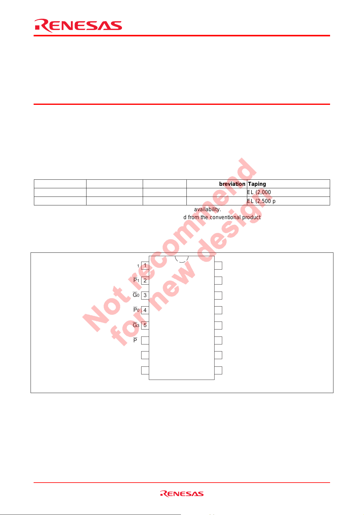
Pin Arrangement
G
P
G
P
G
P
GND
1
1
1
2
0
3
0
4
3
5
3
6
7
P
8
(Top view)
16
15
14
13
12
11
10
V
CC
P
2
G
2
C
n
C
n+X
C
n+y
G
9
n+z
C
Rev.2.00, Jul.16.2004, page 1 of 6
Page 2
HD74AC182
Logic Symbol
P
0
G0P1G
C
n
C
Pin Names
Cn Carry Input
G
, G
0
2
G
1
G
3
P
, P
0
1
P
2
P
3
C
to C
n + x
G Carry Generate Output (Active Low)
P Carry Propagate Output (Active Low)
Carry Generate Inputs (Active Low)
Carry Generate Input (Active Low)
Carry Generate Input (Active Low)
Carry Propagate Inputs (Active Low)
Carry Propagate Input (Active Low)
Carry Propagate Input (Active Low)
Carry Outputs
n + z
n+x
1
C
n+y
P2G
2
P3G
3
G
P
C
n+z
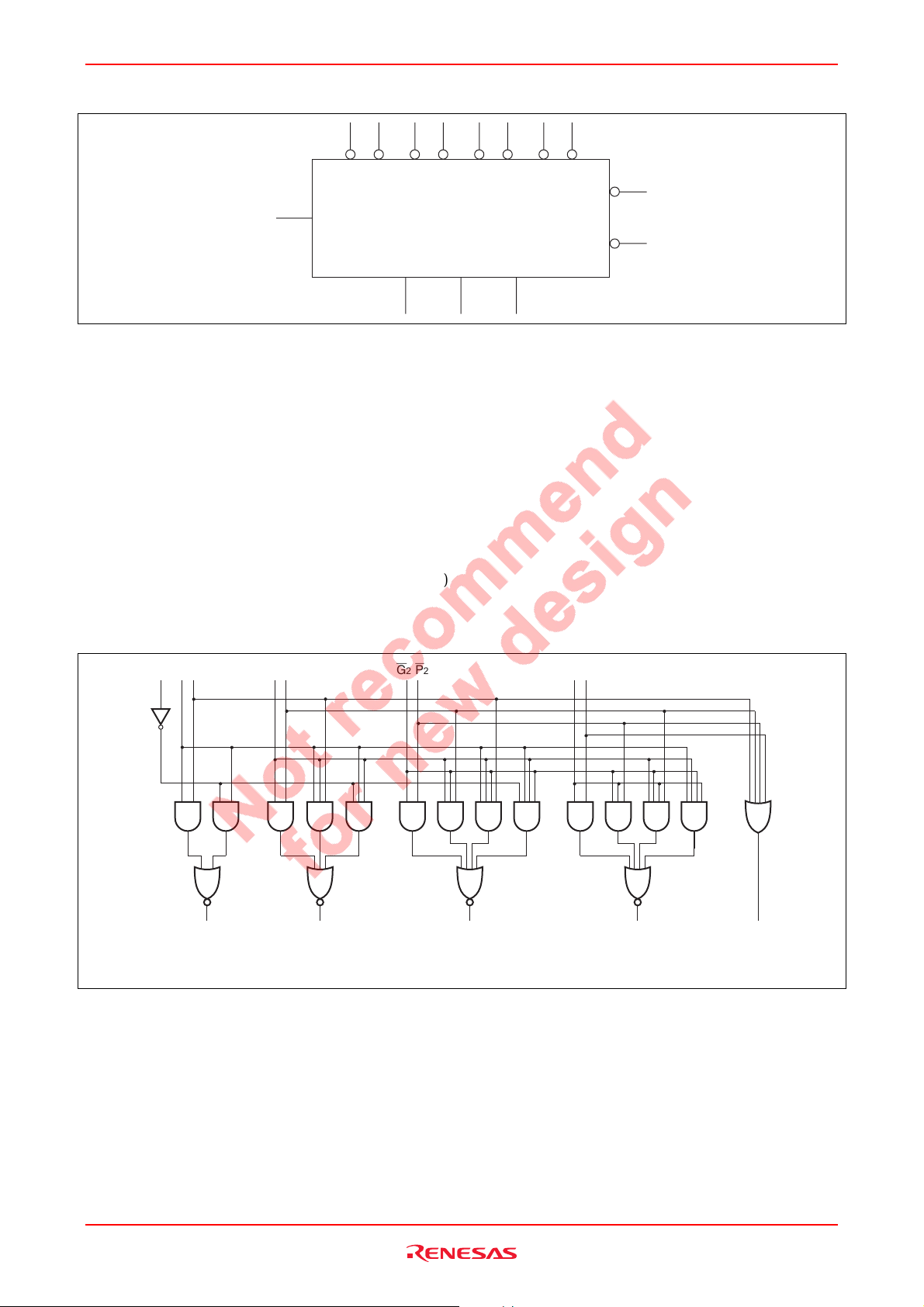
Logic Diagram
C
n
G0P
0
C
n+x
G
1
P
1
C
n+y
G2P
2
C
n+z
G3P
3
GP
Please note that this diagram is provided only for the understanding of logic operations and should not be
used to estimate propagation delays.
Functional Description
The HD74AC182/HD74ACT182 carry lookahead generator accepts up to four pairs of Active Low Carry Propagate (P
to P3) and Carry Generate (G0 to G3) signals and an Active High Carry input (Cn) and provides anticipated Active High
carries (C
Carry Propagate (P) and Carry Generate (G) outputs which may be used for further level of lookahead. The logic
equations provided at the outputs are:
n + x
, C
n + y
, C
) across four groups of binary adders. The HD74AC182/HD74ACT182 also has Active Low
n + z
0
Rev.2.00, Jul.16.2004, page 2 of 6
Page 3

HD74AC182
C
= G0 + P0C
n + x
C
= G1 + P1G0 + P1P0C
n + y
C
= G2 + P2G1 + P2P1G0 + P2P1P0C
n + z
G = G
P = P
3P2P1P0
n
n
+ P3G2 + P3P2G1 + P3P2P1G
3
n
0
Also, the HD74AC182/HD74ACT182 can be used with binary ALUs in an active Low or active High input operand
mode. The connections (Figure a) to and from the ALU to the carry lookahead generator are identical in both cases.
Carries are rippled between lookahead blocks. The critical speed path follows the circled numbers. There are several
possible arrangements for the carry interconnects, but all achieve about the same speed. A 28-bit ALU is formed by
dropping the last HD74AC182/HD74ACT182.
Truth Table
Inputs Outputs
C
GGGG
n
PPPP
0
GGGG
0
PPPP
1
GGGG
1
PPPP
2
GGGG
2
PPPP
3
XHH L
LHX L
XLX H
HXL H
XXXHH L
XHHHX L
LHXHX L
XXXLX H
XLXXL H
HXLXL H
XXXXXHH L
XXXHHHX L
XHHHXHX L
LHXHXHX L
XXXXXLX H
XXXLXXL H
XLXXLXL H
HXLXLXL H
X XXXXHH H
X XXHHHX H
XHHHXHX H
HHXHXHX H
X XXXXLX L
XXXLXXL L
XLXXLXL L
LXLXLXL L
HXXX H
XHXX H
XXHX H
XXXH H
LLLL L
H : High Voltage Level
L : Low Voltage Level
X : Immaterial
C
3
n + x
C
n + y
C
n + z
GGGGP
P
PP
Rev.2.00, Jul.16.2004, page 3 of 6
Page 4

HD74AC182
Absolute Maximum Ratings
Item Symbol Ratings Unit Condition
Supply voltage V
CC
IK
–0.5 to 7 V
–20 mA VI = –0.5VDC input diode current I
20 mA VI = Vcc+0.5V
DC input voltage V
I
OK
–0.5 to Vcc+0.5 V
–50 mA VO = –0.5VDC output diode current I
50 mA VO = Vcc+0.5V
DC output voltage V
DC output source or sink current I
O
O
DC VCC or ground current per output pin ICC, I
GND
–0.5 to Vcc+0.5 V
±50 mA
±50 mA
Storage temperature Tstg –65 to +150 °C
Recommended Operating Conditions
Item Symbol Ratings Unit Condition
Supply voltage V
Input and output voltage VI, V
CC
O
Operating temperature Ta –40 to +85 °C
Input rise and fall time
tr, tf 8 ns/V
(except Schmitt inputs)
V
30% to 70% V
IN
CC
2 to 6 V
0 to V
CC
V
VCC = 3.0V
VCC = 4.5 V
= 5.5 V
V
CC
DC Characteristics
Item Sym-
Input Voltage
V
bol
IH
Vcc
(V)
3.0 2.1 1.5 — 2.1 —
4.5 3.15 2.25 — 3.15 —
5.5 3.85 2.75 — 3.85 —
V
3.0 — 1.50 0.9 — 0.9
IL
4.5 — 2.25 1.35 — 1.35
5.5 — 2.75 1.65 — 1.65
Output voltage
V
3.0 2.9 2.99 — 2.9 —
OH
4.5 4.4 4.49 — 4.4 —
5.5 5.4 5.49 — 5.4 —
3.0 2.58 — — 2.48 — IOH = –12 mA
4.5 3.94 — — 3.80 — IOH = –24 mA
5.5 4.94 — — 4.80 —
V
3.0 — 0.002 0.1 — 0.1
OL
4.5 — 0.001 0.1 — 0.1
5.5 — 0.001 0.1 — 0.1
3.0 — — 0.32 — 0.37 IOL = 12 mA
4.5 — — 0.32 — 0.37 IOL = 24 mA
5.5 — — 0.32 — 0.37
Input leakage
I
IN
5.5 — — ±0.1 — ±1.0 µAVIN = VCC or GND
current
Dynamic output
current*
Quiescent supply
I
I
I
OLD
OHD
CC
5.5———86—mAV
5.5 — — — –75 — mA V
5.5 — — 8.0 — 80 µAVIN = VCC or ground
current
*Maximum test duration 2.0 ms, one output loaded at a time.
Ta = 25°°°°C Ta = –40 to
min. typ. max. min. max.
+85°°°°C
Unit Condition
V
V
= 0.1 V or VCC –0.1 V
OUT
V
= 0.1 V or VCC –0.1 V
OUT
V
VIN = VIL or V
I
= –50 µA
OUT
VIN = VIL or V
IH
IH
IOH = –24 mA
VIN = VIL or V
I
= 50 µA
OUT
VIN = VIL or V
IH
IH
IOL = 24 mA
= 1.1 V
OLD
= 3.85 V
OHD
Rev.2.00, Jul.16.2004, page 4 of 6
Page 5

HD74AC182
AC Characteristics
Ta = +25°C
C
= 50 pF
L
Ta = –40°C to +85°C
CL = 50 pF
Item Symbol VCC (V)*1Min Typ Max Min Max Unit
Propagation delay t
PLH
3.3 1.0 8.0 10.5 1.0 11.5 ns
Pn to P 5.0 1.0 5.5 8.0 1.0 9.0
Propagation delay t
PHL
3.3 1.0 8.0 10.5 1.0 11.5 ns
Pn to P 5.0 1.0 5.5 8.0 1.0 9.0
Propagation delay t
Cn to C
n + x, y, z
Propagation delay t
Cn to C
n + x, y, z
Propagation delay t
Pn or Gn to C
n + x, y, z
Propagation delay t
Pn or Gn to C
n + x, y, z
PLH
PHL
PLH
PHL
3.3 1.0 9.5 12.0 1.0 13.0 ns
5.0 1.0 7.5 10.0 1.0 11.0
3.3 1.0 9.0 12.0 1.0 13.0 ns
5.0 1.0 7.0 10.0 1.0 11.0
3.3 1.0 10.5 13.0 1.0 14.0 ns
5.0 1.0 8.0 10.5 1.0 11.5
3.3 1.0 11.5 14.0 1.0 15.5 ns
5.0 1.0 9.0 11.5 1.0 12.5
Note: 1. Voltage Range 3.3 is 3.3 V ± 0.3 V
Voltage Range 5.0 is 5.0 V ± 0.5 V
Capacitance
Item Symbol Typ Unit Condition
Input capacitance C
Power dissipation capacitance C
IN
PD
4.5 pF VCC = 5.5 V
50.0 pF VCC = 5.0 V
Rev.2.00, Jul.16.2004, page 5 of 6
Page 6

HD74AC182
Package Dimensions
16
10.06
10.5 Max
As of January, 2003
Unit: mm
9
5.5
*Ni/Pd/Au plating
1
0.80 Max
1.27
*0.40 ± 0.06
10.3 Max
16
9.9
8
0.10 ± 0.10
0.15
0.12
9
2.20 Max
M
7.80
1.15
*0.20 ± 0.05
0.70 ± 0.20
Package Code
JEDEC
JEITA
(reference value)
Mass
+ 0.20
– 0.30
0˚ – 8
˚
FP-16DAV
—
Conforms
0.24 g
As of January, 2003
Unit: mm
*Ni/Pd/Au plating
1
1.27
0.635 Max
*0.40 ± 0.06
8
0.25
+ 0.11
– 0.04
0.14
0.15
3.95
1.75 Max
M
+ 0.10
6.10
– 0.30
1.08
*0.20 ± 0.05
+ 0.67
0.60
– 0.20
Package Code
JEDEC
JEITA
(reference value)
Mass
0˚ – 8
˚
FP-16DNV
Conforms
Conforms
0.15 g
Rev.2.00, Jul.16.2004, page 6 of 6
Page 7

Sales Strategic Planning Div. Nippon Bldg., 2-6-2, Ohte-machi, Chiyoda-ku, Tokyo 100-0004, Japan
Keep safety first in your circuit designs!
1. Renesas Technology Corp. puts the maximum effort into making semiconductor products better and more reliable, but there is always the possibility that trouble
may occur with them. Trouble with semiconductors may lead to personal injury, fire or property damage.
Remember to give due consideration to safety when making your circuit designs, with appropriate measures such as (i) placement of substitutive, auxiliary
circuits, (ii) use of nonflammable material or (iii) prevention against any malfunction or mishap.
Notes regarding these materials
1. These materials are intended as a reference to assist our customers in the selection of the Renesas Technology Corp. product best suited to the customer's
application; they do not convey any license under any intellectual property rights, or any other rights, belonging to Renesas Technology Corp. or a third party.
2. Renesas Technology Corp. assumes no responsibility for any damage, or infringement of any third-party's rights, originating in the use of any product data,
diagrams, charts, programs, algorithms, or circuit application examples contained in these materials.
3. All information contained in these materials, including product data, diagrams, charts, programs and algorithms represents information on products at the time of
publication of these materials, and are subject to change by Renesas Technology Corp. without notice due to product improvements or other reasons. It is
therefore recommended that customers contact Renesas Technology Corp. or an authorized Renesas Technology Corp. product distributor for the latest product
information before purchasing a product listed herein.
The information described here may contain technical inaccuracies or typographical errors.
Renesas Technology Corp. assumes no responsibility for any damage, liability, or other loss rising from these inaccuracies or errors.
Please also pay attention to information published by Renesas Technology Corp. by various means, including the Renesas Technology Corp. Semiconductor
home page (http://www.renesas.com).
4. When using any or all of the information contained in these materials, including product data, diagrams, charts, programs, and algorithms, please be sure to
evaluate all information as a total system before making a final decision on the applicability of the information and products. Renesas Technology Corp. assumes
no responsibility for any damage, liability or other loss resulting from the information contained herein.
5. Renesas Technology Corp. semiconductors are not designed or manufactured for use in a device or system that is used under circumstances in which human life
is potentially at stake. Please contact Renesas Technology Corp. or an authorized Renesas Technology Corp. product distributor when considering the use of a
product contained herein for any specific purposes, such as apparatus or systems for transportation, vehicular, medical, aerospace, nuclear, or undersea repeater
use.
6. The prior written approval of Renesas Technology Corp. is necessary to reprint or reproduce in whole or in part these materials.
7. If these products or technologies are subject to the Japanese export control restrictions, they must be exported under a license from the Japanese government and
cannot be imported into a country other than the approved destination.
Any diversion or reexport contrary to the export control laws and regulations of Japan and/or the country of destination is prohibited.
8. Please contact Renesas Technology Corp. for further details on these materials or the products contained therein.
RENESAS SALES OFFICES
Renesas Technology America, Inc.
450 Holger Way, San Jose, CA 95134-1368, U.S.A
Tel: <1> (408) 382-7500 Fax: <1> (408) 382-7501
Renesas Technology Europe Limited.
Dukes Meadow, Millboard Road, Bourne End, Buckinghamshire, SL8 5FH, United Kingdom
Tel: <44> (1628) 585 100, Fax: <44> (1628) 585 900
Renesas Technology Europe GmbH
Dornacher Str. 3, D-85622 Feldkirchen, Germany
Tel: <49> (89) 380 70 0, Fax: <49> (89) 929 30 11
Renesas Technology Hong Kong Ltd.
7/F., North Tower, World Finance Centre, Harbour City, Canton Road, Hong Kong
Tel: <852> 2265-6688, Fax: <852> 2375-6836
Renesas Technology Taiwan Co., Ltd.
FL 10, #99, Fu-Hsing N. Rd., Taipei, Taiwan
Tel: <886> (2) 2715-2888, Fax: <886> (2) 2713-2999
Renesas Technology (Shanghai) Co., Ltd.
26/F., Ruijin Building, No.205 Maoming Road (S), Shanghai 200020, China
Tel: <86> (21) 6472-1001, Fax: <86> (21) 6415-2952
Renesas Technology Singapore Pte. Ltd.
1, Harbour Front Avenue, #06-10, Keppel Bay Tower, Singapore 098632
Tel: <65> 6213-0200, Fax: <65> 6278-8001
© 2004. Renesas Technology Corp., All rights reserved. Printed in Japan.
http://www.renesas.com
Colophon .1.0
 Loading...