

Page 1
REJ09B0054-0500
The revision list can be viewed directly by
clicking the title page.
The revision list summarizes the locations of
revisions and additions. Details should always
be checked by referring to the relevant text.
H8S/2258, H8S/2239, H8S/2238,
16
Renesas 16-Bit Single-Chip Microcomputer
H8S/2258 HD64F2258 H8S/2236R HD6432236R
H8S/2256 HD6432256 HD6432237
H8S/2239 HD64F2239 H8S/2233 HD6432233
H8S/2238B HD64F2238B H8S/2225 HD6432225
H8S/2238R HD64F2238R
H8S/2236B HD6432236B
H8S/2237, H8S/2227
Groups
Hardware Manual
H8S Family/H8S/2200 Series
HD6432258 HD6432236RW
HD6432258W H8S/2237 HD6472237
HD6432256W H8S/2235 HD6432235
HD6432239 H8S/2227 HD64F2227
HD6432239W HD6432227
HD6432238B H8S/2224 HD6432224
HD6432238BW H8S/2223 HD6432223
HD6432238R
HD6432238RW
HD6432236BW
Rev. 5.00
Revision Date: Aug 08, 2006
Page 2

Keep safety first in your circuit designs!
1. Renesas Technology Corp. puts the maximum effort into making semiconductor products better and
more reliable, but there is always the possibility that trouble may occur with them. Trouble with
semiconductors may lead to personal injury, fire or property damage.
Remember to give due consideration to safety when making your circuit designs, with appropriate
measures such as (i) placement of substitutive, auxiliary circuits, (ii) use of nonflammable material or
(iii) prevention against any malfunction or mishap.
Notes regarding these materials
1. These materials are intended as a reference to assist our customers in the selection of the Renesas
Technology Corp. product best suited to the customer's application; they do not convey any license
under any intellectual property rights, or any other rights, belonging to Renesas Technology Corp. or
a third party.
2. Renesas Technology Corp. assumes no responsibility for any damage, or infringement of any thirdparty's rights, originating in the use of any product data, diagrams, charts, programs, algorithms, or
circuit application examples contained in these materials.
3. All information contained in these materials, including product data, diagrams, charts, programs and
algorithms represents information on products at the time of publication of these materials, and are
subject to change by Renesas Technology Corp. without notice due to product improvements or
other reasons. It is therefore recommended that customers contact Renesas Technology Corp. or
an authorized Renesas Technology Corp. product distributor for the latest product information
before purchasing a product listed herein.
The information described here may contain technical inaccuracies or typographical errors.
Renesas Technology Corp. assumes no responsibility for any damage, liability, or other loss rising
from these inaccuracies or errors.
Please also pay attention to information published by Renesas Technology Corp. by various means,
including the Renesas Technology Corp. Semiconductor home page (http://www.renesas.com).
4. When using any or all of the information contained in these materials, including product data,
diagrams, charts, programs, and algorithms, please be sure to evaluate all information as a total
system before making a final decision on the applicability of the information and products. Renesas
Technology Corp. assumes no responsibility for any damage, liability or other loss resulting from the
information contained herein.
5. Renesas Technology Corp. semiconductors are not designed or manufactured for use in a device or
system that is used under circumstances in which human life is potentially at stake. Please contact
Renesas Technology Corp. or an authorized Renesas Technology Corp. product distributor when
considering the use of a product contained herein for any specific purposes, such as apparatus or
systems for transportation, vehicular, medical, aerospace, nuclear, or undersea repeater use.
6. The prior written approval of Renesas Technology Corp. is necessary to reprint or reproduce in
whole or in part these materials.
7. If these products or technologies are subject to the Japanese export control restrictions, they must
be exported under a license from the Japanese government and cannot be imported into a country
other than the approved destination.
Any diversion or reexport contrary to the export control laws and regulations of Japan and/or the
country of destination is prohibited.
8. Please contact Renesas Technology Corp. for further details on these materials or the products
contained therein.
Rev. 5.00 Aug 08, 2006 page ii of lxxxvi
Page 3

General Precautions on Handling of Product
1. Treatment of NC Pins
Note: Do not connect anything to the NC pins.
The NC (not connected) pins are either not connected to any of the internal circuitry or are
used as test pins or to reduce noise. If something is connected to the NC pins, the
operation of the LSI is not guaranteed.
2. Treatment of Unused Input Pins
Note: Fix all unused input pins to high or low level.
Generally, the input pins of CMOS products are high-impedance input pins. If unused pins
are in their open states, intermediate levels are induced by noise in the vicinity, a passthrough current flows internally, and a malfunction may occur.
3. Processing before Initialization
Note: When power is first supplied, the product’s state is undefined.
The states of internal circuits are undefined until full power is supplied throughout the
chip and a low level is input on the reset pin. During the period where the states are
undefined, the register settings and the output state of each pin are also undefined. Design
your system so that it does not malfunction because of processing while it is in this
undefined state. For those products which have a reset function, reset the LSI immediately
after the power supply has been turned on.
4. Prohibition of Access to Undefined or Reserved Addresses
Note: Access to undefined or reserved addresses is prohibited.
The undefined or reserved addresses may be used to expand functions, or test registers
may have been be allocated to these addresses. Do not access these registers; the system’s
operation is not guaranteed if they are accessed.
Rev. 5.00 Aug 08, 2006 page iii of lxxxvi
Page 4

Configuration of This Manual
This manual comprises the following items:
1. General Precautions on Handling of Product
2. Configuration of This Manual
3. Preface
4. Main Revisions in This Edition
The list of revisions is a summary of points that have been revised or added to earlier versions.
This does not include all of the revised contents. For details, see the actual locations in this
manual.
5. Contents
6. Overview
7. Description of Functional Modules
• CPU and System-Control Modules
• On-Chip Peripheral Modules
The configuration of the functional description of each module differs according to the
module. However, the generic style includes the following items:
i) Feature
ii) Input/Output Pin
iii) Register Description
iv) Operation
v) Usage Note
When designing an application system that includes this LSI, take notes into account. Each section
includes notes in relation to the descriptions given, and usage notes are given, as required, as the
final part of each section.
8. List of Registers
9. Electrical Characteristics
10. Appendix
11. Index
Rev. 5.00 Aug 08, 2006 page iv of lxxxvi
Page 5

Preface
The H8S/2558 Group, H8S/2239 Group, H8S/2238 Group, H8S/2237 Group, and H8S/2227
Group are high-performance microcomputers made up of the internal 32-bit configuration
H8S/2000 CPU as their cores, and the peripheral functions required to configure a system.
TM
*
A single-power flash memory (F-ZTAT
these LSIs’ ROM. These versions provide flexibility as they can be reprogrammed in no time to
cope with all situations from the early stages of mass production to full-scale mass production.
This is particularly applicable to application devices of which the specifications frequently
changeable.
On-chip peripheral functions of each microcomputer are summarized below.
Note: * F-ZTAT is a trademark of Renesas Technology Corp.
) version and masked ROM version are available for
Rev. 5.00 Aug 08, 2006 page v of lxxxvi
Page 6

List of On-Chip Peripheral Functions:
Group Name
Microcomputer
H8S/2258
Group
H8S/2258
H8S/2256
H8S/2239
Group
H8S/2239
H8S/2238
Group
H8S/2238B
H8S/2238R
H8S/2236B
H8S/2236R
H8S/2237
Group
H8S/2237
H8S/2235
H8S/2233
H8S/2227
Group
H8S/2227
H8S/2225
H8S/2224
H8S/2223
Bus controller (BSC) O (16 bits) O (16 bits) O (16 bits) O (16bits) O (16 bits)
Data transfer controller
OOOOO
(DTC)
DMA controller (DMAC) O
PC break controller (PBC) ×2 ×2 ×2 ×2 ×2
16-bit timer pulse unit
×6 ×6 ×6 ×6 ×3
(TPU)
8-bit timer (TMR) ×4 ×4 ×4 ×2 ×2
Watchdog timer (WDT) ×2 ×2 ×2 ×2 ×2
Serial communication
×4 ×4 ×4 ×4 ×3
interface (SCI)
2
I
C bus interface (IIC) ×2 (option) ×2 (option) ×2 (option)
D/A converter ×2 ×2 ×2 ×2
A/D
Analog input ×8 ×8 ×8 ×8 ×8
converter
IEBus* controller (IEB) ×1
Note: * IEBus (Inter Equipment Bus) is a trademark of NEC Electronics Corp.
Target Users: This manual was written for users who will be using the H8S/2258 Group,
H8S/2239 Group, H8S/2238 Group, H8S/2237 Group, and H8S/2227 Group in the
design of application systems. Target users are expected to understand the
fundamentals of electrical circuits, logical circuits, and microcomputers.
Objective: This manual was written to explain the H8S/2258 Group, H8S/2239 Group,
H8S/2238 Group, H8S/2237 Group, and H8S/2227 Group hardware functions and
electrical characteristics of this LSI to the target users.
Refer to the H8S/2600 Series, H8S/2000 Series Software Manual for a detailed
description of the instruction set.
Rev. 5.00 Aug 08, 2006 page vi of lxxxvi
Page 7

Notes on reading this manual:
• In order to understand the overall functions of the chip
Read the manual according to the contents. This manual can be roughly categorized into
descriptions on the CPU, system control functions, peripheral functions, and electrical
characteristics.
• In order to understand the details of the CPU’s functions
Read the H8S/2600 Series, H8S/2000 Series Software Manual.
• In order to understand the details of a register whole name is already known
Read the index that is the final part of the manual to find the page number of the entry on the
register. The addresses, bits, and initial values of the registers are summarized in section 26,
List of Registers.
Rules: Register name: The following notation is used for cases when the same or a
similar function, e.g., 16-bit timer pulse unit or serial
communication, is implemented on more than one channel:
XXX_N (XXX is the register name and N is the channel
number)
Bit order: The MSB is on the left and the LSB is on the right.
Number notation: Binary is B'xxxx, hexadecimal is H'xxxx, and decimal is
xxxx.
Signal notation: An overbar is added to a low-active signal: xxxx
Related Manuals: The latest versions of all related manuals are available from our web site.
Please ensure you have the latest versions of all documents.
http://www.renesas.com/
H8S/2258 Group, H8S/2239 Group, H8S/2238 Group, H8S/2237 Group, H8S/2227 Group
manuals:
Document Title Document No.
H8S/2258 Group, H8S/2239 Group, H8S/2238 Group, H8S/2237 Group,
H8S/2227 Group Hardware Manual
H8S/2600 Series, H8S/2000 Series Software Manual REJ09B0139
Rev. 5.00 Aug 08, 2006 page vii of lxxxvi
This manual
Page 8

User's Manuals for Development Tools:
Document Title Document No.
H8S, H8/300 Series C/C++ Compiler, Assembler, Optimized Linkage
Editor Compiler Package Ver. 6.01 User's Manual
H8S, H8/300 Series High-performance Embedded Workshop 3
Tutorial
H8S, H8/300 Series High-performance Embedded Workshop 3
User's Manual
High-performance Embedded Workshop V.4.00 User's Manual REJ10J0886
REJ10B0161
REJ10B0024
REJ10B0026
Application Notes:
Document Title Document No.
H8S, H8/300 Series C/C++ Compiler Package Application Note REJ05B0464
Rev. 5.00 Aug 08, 2006 page viii of lxxxvi
Page 9
Main Revisions for This Edition
Item Page Revision (See Manual for Details)
All Description of "under development" for HD64F2239 deleted
1.1 Features 2
1.3.1 Pin Arrangement
Figure 1.11 Pin
Arrangement of H8S/2238
Group (FP-100A, FP-100AV:
Top View, Only for
H8S/2238B
and H8S/2236B)
• On-chip memory
Table amended
ROM Model ROM RAM Remarks
version
3
• Compact package
Package (Code)
TQFP-100 TFP-100B,
TQFP-100
QFP-100
QFP-100
LFBGA-112
TFBGA-112
HD6432258 256 kbytes 16 kbytesMasked ROM
HD6432258W 256 kbytes 16 kbytes
HD6432256 128 kbytes 8 kbytes
HD6432256W 128 kbytes 8 kbytes
6
*
4
5
TFP-100BV
TFP-100G,
TFP-100GV
FP-100A, FP-100AV
FP-100B, FP-100BV
BP-112, BP-112V
TBP-112A,
TBP-112AV
1
*
2
*
3
*
*
*
Notes amended
1. Not supported by the H8S/2258 Group.
Notes:
2. Supported only by the H8S/2258 Group, H8S/2238B,
H8S/2236B, H8S/2237 Group, and HD6432227.
3. Not supported by the HD64F2227.
4. Supported only by the HD64F2238R.
5. Supported only by the HD64F2238R and HD64F2239.
6. Package code ending in the letter V designate Pb-free
Product.
14 Figure 1.11 title amended
Rev. 5.00 Aug 08, 2006 page ix of lxxxvi
Page 10
Item Page Revision (See Manual for Details)
1.3.1 Pin Arrangement
19 Figure 1.16 title amended
Figure 1.16 Pin
Arrangement of H8S/2227
Group (FP-100A, FP-100AV:
Top View, Only for
HD6432227)
Table 1.3 Pin Arrangements
in Each Mode of H8S/2238
Group
1.3.2 Pin Arrangement in
Each Mode
33 Notes amended
Notes: 1. Supported only by H8S/
2. Supported only by the
in the H8S/2238B and H8S/2236B.
3. V
CC
39 to43Table 1.5 amended
1
*
FP-100B
FP-100BV
HD64F2238R.
1
*
FP-100A
Table 1.5 Pin Arrangements
in Each Mode of H8S/2227
Group
41 Table 1.5 amended
Pin No. Pin Name
TFP-100B
TFP-100BV
TFP-100G
TFP-100GV
1
*
FP-100B
*
FP-100BV
57 60 OSC2 OSC2 OSC2 OSC2 NC
58 61 OSC1 OSC1 OSC1 OSC1 VSS
59 62 RES RES RES RES RES
FP-100A
1
FP-100AV
2
*
2
*
Mode 4 Mode 5 Mode 6 Mode 7
43 Note 2 added
1. Supported only by masked ROM version.
Notes:
2. Supported only by the HD6432227.
1.3.3 Pin Functions
Table 1.6 Pin Functions of
H8S/2258 Group
45 Table 1.6 amended
RES* STBY* NMI
49
Note: * Measures should be taken to deal with noise, which
*
can cause operation errors otherwise.
Table 1.7 Pin Functions of
H8S/2239 Group and
H8S/2238 Group
50 Table 1.7 amended
CVCC in power supply
... (H8S/2239, H8S/2378R
, and H8S/2236R used), ...
51 Table 1.7 amended
RES
5
*
STBY
5
*
NMI
5
*
2238B and H8S/2236B.
2
*
FP-100BAV
2
*
Flash Memory
Programmable
Mode
Rev. 5.00 Aug 08, 2006 page x of lxxxvi
Page 11
Item Page Revision (See Manual for Details)
1.3.3 Pin Functions
Table 1.7 Pin Functions of
H8S/2239 Group and
H8S/2238 Group
53
Type Symbol
DMA
DREQ1
controller
DREQ08990
2
*
(DMAC)
TEND1
TEND08788
DACK1
DACK03534
TFP-100B
TFP-100BV
TFP-100G
TFP-100GV
FP-100B
FP-100BV
Pin No.
3
*
FP-100A
3
*
FP-100AV
B6
C6
J5
1
*
BP-112
1
*
BP-112V
4
*
TBP-112A
4
*
TBP-112AV
I/O Function
Input Request DMAC activation.
D6
Output Indicate that the DMAC has ended
A6
Output These pins function as single address
H5
55 P47 to P40 in I/O ports
L10, L9, K11, K10, K9, K8, H7, J8
56 Notes: 1. Supported only by the HD64F2238R.
2. Supported only by the H8S/2239 Group.
3. Supported only by the H8S/2238B
4. Supported only by the
HD64F2238R and HD64F2239.
5. Measures should be taken to deal with noise, which can
cause operation errors otherwise.
Table 1.8 Pin Functions of
H8S/2237 Group and
H8S/2227 Group
57 to61Table 1.8 amended
1
*
3
*
STBY
FP-100BV
3
*
NMI
FP-100B
RES
1
*
FP-100A
3
*
61 Notes amended
1. Supported only by masked ROM version.
Notes:
2. Supported only by the HD6432227.
3. Measures should be taken to deal with noise, which can
cause operation errors otherwise.
3.4 Memory Map in Each
Operating Mode
115 Figure 3.7 amended
(Before) On-chip R
AM → (After) On-chip ROM
Figure 3.7 H8S/2235 and
H8S/2225 Memory Map in
Each Operating Mode
5.1 Features
Figure 5.1 Block Diagram of
128 Figure 5.1 amended
(Before)
IRQ → (After) IRQ
Interrupt Controller
5.3.2 IRQ Enable Register
(IER)
131 Description amended
(Before)
IRQn → (After) IRQn
(Supported only by the H8S/2239 Group.)
transmitting data.
(Supported only by the H8S/2239 Group.)
transmitting acknowledge of DMAC.
(Supported only by the H8S/2239 Group.)
and H8S/2236B.
2
*
FP-100BAV
2
*
Rev. 5.00 Aug 08, 2006 page xi of lxxxvi
Page 12
Item Page Revision (See Manual for Details)
5.3.4 IRQ Status Register
(ISR)
134 Description amended
ISR indicates the status of IRQn (n=7 to 0) interrupt
requests.
6.3.4 Operation in Transition
to Power-Down Modes
161,
162
Description amended
• When the SLEEP instruction causes a transition from
high-speed (medium-speed) mode to sleep mode
from subactive mode to subsleep mode: After execution
of the SLEEP instruction, a transition is not made to
sleep mode or subsleep mode, and PC break interrupt
handling is executed. ...
• When the SLEEP instruction causes a transition to
software standby mode or watch mode:
8.3 Register Descriptions 205 Description amended
TCR_0A)
TCR_0B)
8.7.1 DMAC Register
Access during Operation
• Transfer count register_0A (E
• Transfer count register_0B (E
276 Figure 8.38 amended
DMA last transfer cycle
Figure 8.38 DMAC
Register Update Timing
DMA read
DMA write
DMA
dead
, or
Transfer
destination
[2'] [3]
G, DTCERI
9.1 Features
Figure 9.1 Block Diagram of
DTC
nsfer
urce
ead
282 Figure 9.1 amended
(Before) DTCERA to DTCER
to DTCER
9.2 Register Descriptions 283 Description amended
... When activated, ... back to the RAM.
• DTC Enable Registers A to G, and I (DCTERA to
DTCERG, and DTCERI) ...
Rev. 5.00 Aug 08, 2006 page xii of lxxxvi
DeadWrite
Idle
F, DTCERI → (After) DTCERA
Page 13
Item Page Revision (See Manual for Details)
t
9.2.7 DTC Enable Registers
A to G, and I
9.2.8 DTC Vector Register
(DTVECR)
9.4 Location of Register
Information and DTC Vector
Table
286,
287
Section 9.2.7 description replaced and bit table amended
9.2.7 DTC Enable Registers A to G, and I (DTCERA to DTCERG, and DTCERI)
DTCER is a set of registers to specify the DTC activation interrupt source, and comprised of eigh
registers; DTCERA to DTCERG, and DTCERI. The correspondence between interrupt sources
and DTCE bits, and vector numbers generated by the interrupt controller are shown in table 9.2.
For DTCE bit setting, use bit manipulation instructions such as BSET and BCLR for reading and
writing. When multiple activation sources are to be set at one time, only at the initial setting,
writing data is enabled after executing a dummy read on the relevant register with all the interrupt
being masked.
Bit Bit Name
7
DTCEn7
6
DTCEn6
5
DTCEn5
4
DTCEn4
3
DTCEn3
2
DTCEn2
1
DTCEn1
0
DTCEn0
Note: n = A to G, and I
Initial
Value R/W Description
0
R/W
0
0
0
0
0
0
0
DTC Activation Enable
R/W
0: Disables an interrupt for DTC activation.
R/W
1: Specifies a relevant interrupt source as a DTC
activation source.
R/W
[Clearing conditions]
R/W
• When the DISEL bit is 1 and the data transfer
R/W
has ended
R/W
• When the specified number of transfers have
R/W
ended
[Retaining condition]
When the DISEL bit is 0 and the specifiednumber
of transfers have not been completed
288 Bit table amended
Bit Bit Name
7SWDTE 0 R/W DTC Software Activation Enable
Initial
Value R/W Description
Enables or disables the DTC software activation.
0: Disables the DTC software activation.
1: Enables the DTC software activation.
[Clearing conditions]
• When the DISEL bit is 0 and the specified
number of transfers have not ended
• When 0 is written to the DISEL bit after a
software-activated data transfer end interrupt
(SWDTEND) request has been sent to the CPU.
[Retaining conditions]
• When the DISEL bit is 1 and data transfer has
ended
• When the specified number of transfers have
ended
• When the software-activated data transfer is in
process
293 DTCE description of IERxI (RxRDY) and IETxI (TxRDY)
amended
EG6 DTCEG5
DTC
Table 9.2 Interrupt Sources,
DTC Vector Addresses, and
Corresponding DTCEs
Rev. 5.00 Aug 08, 2006 page xiii of lxxxvi
Page 14
Item Page Revision (See Manual for Details)
9.8.2 On-Chip RAM 304 Description amended
The MRA, ... in the on-chip RAM. When the DTC is used,
the RAME bit in SYSCR should not be cleared to 0.
Section 10 I/O Ports
Table 10.1 Port Functions
306 Port 3 input/output and output type description amended
1
... NMOS push-pull output*
(P35, P34, SCK1)
10.2 Port 3 315 Description amended
Port 3 is ... following registers. The P34, P35,
function as NMOS push/pull outputs.*
10.2.5 Pin Functions 317 Description amended
As shown in figure 10.1, when the pins P35, P34,
SCK0
, or SDA0 type open drain output is used, ...
and SCK1
SCK1,
Figure 10.1 Types of Open
318 Figure 10.1 amended
Drain Outputs
318 Description amended
319 Table amended
320
10.4.4 Pin Functions 324
(a) Open drain output type for P34, P35,
SCK1, SCL0, and
SDA0 pins
P2 V
(Before) ... output the
level.
V
CC
level. → (After) ... output the
CC
• P35/SCK1/SCL0/IRQ5
SCK1
input pin SCL0 I/O pin*
3
• P34/RxD1/SDA0
SDA0 I/O pin*
2
• P33/TxD1/SCL1
2
SCL1 I/O pin
*
• P32/SCK0/SDA0
SDA1 I/O pin*
3
• P75/TMO3/SCK3
Description amended
... OS3 to OS0 bits in TCSR_3 of TMR_3
*, CKE1 and ...
Table amended
OS3 to OS0
* TMO3* output pin
Note added
Note: * Not available in the H8S/2237 Group and H8S/2227
Group.
Rev. 5.00 Aug 08, 2006 page xiv of lxxxvi
Page 15
Item Page Revision (See Manual for Details)
10.4.4 Pin Functions 325
• P74/TMO2/MRES
Description amended
... OS3 to OS0 bits in TCSR_2 of TMR_2
Table amended
OS3 to OS0
* TMO2* output
Note added
Note: * Not available in the H8S/2237 Group and H8S/2227
Group.
325
• P73/TMO1/TEND1/CS7
Description amended
... DMATCR of DMAC
*, OS3 to OS0 ...
Table amended
* output pin
325
TEND1
• P72/TMO0/TEND0/CS6
Description amended
... DMATCR of DMAC
*, OS3 to OS0 ...
Table amended
* output pin
326
TEND0
• P71/TMRI23/TMCI23/DREQ1/CS5
Table amended
Operating
mode Modes 4 to 6 Mode 7
P71DDR0101
P71 input pin CS5 output pin P71 input pin P71 output pinPin functions
DREQ1
TMRI23
TMCI23
*
*
*
2
input pin
1
,
1
,
TMRI23
Note 1 added
1. Not available in the H8S/2237 Group and
Note:
H8S/2227 Group.
326
• P70/TMRI01/TMCI01/DREQ0/CS4
Table amended
TMRI01, TMCI01, DREQ0
* input pin
*, the MRESE ...
1
1
*
*
, TMCI23
, DREQ1
pin
*
2
input
Rev. 5.00 Aug 08, 2006 page xv of lxxxvi
Page 16
Item Page Revision (See Manual for Details)
10.6.6 Pin Functions 330
• PA3/A19/SCK2
Description amended
... SMR_2 of SCI_2
*2, CKE1 and CKE0 bits...
Table amended
Operating mode Modes 4 to 6
AE3 to AE0 B'11xx Other than B'11xx
CKE1 —
2
*
C/A
CKE0 0 1 — —
PA3DDR 0 1 — — —
Pin functions A19
Operating
mode Mode 7
AE3 to AE0
CKE1 0 1
2
*
C/A
CKE0 0 1 ——
PA3DDR 0 1 ———
Pin functions PA3 input pin PA3 output
—
—
—
output
pin
PA3 input
pin
0 1 —
PA3 output
1
*
pin
01—
SCK2
1
*
pin
output pin
Note 2 added
2. Not available in the H8S/2227 Group.
Note:
331
• PA2/A18/RxD2
Description amended
... SCR_2 of SCI_2
*2, and the PA2DDR bit.
Table amended
Operating
mode Modes 4 to 6 Mode 7
AE3 to AE0 B'1011
2
*
RE
PA2DDR 01 01
Pin functions A18
Other than (B'1011 or B'11xx)
or
B'11xx
0101
PA2
PA2
output
pin
input pin
output
pin
RxD2
input pin
1
*
Note 2 added
2. Not available in the H8S/2227 Group.
Note:
0 1
SCK2
output
2
*
2
*
pin
1
*
2
*
1
*
output pin
PA2
input pin
SCK2
SCK2
output
pin
*
*
2
*
output
pin
1
1
PA2
2
*
SCK2
input pin
SCK2
pin
RxD2
input pin
1
*
*
2
input
2
*
2
*
Rev. 5.00 Aug 08, 2006 page xvi of lxxxvi
Page 17
Item Page Revision (See Manual for Details)
10.6.6 Pin Functions 331
• PA1/A17/TxD2
Description amended
... SCR_2 of SCI_2
*2, and the PA1DDR bit.
Table amended
Operating
mode Modes 4 to 6 Mode 7
AE3 to AE0 B'101x or
2
*
TE
PA1DDR 01 01
Pin functions A17
B'11xx
output pin
Other than (B'101x or B'11xx)
01 0 1
PA1
PA1
TxD2
input pin
output
pin
output
1
*
Note 2 added
2. Not available in the H8S/2227 Group.
Note:
10.7.5 Pin Functions 335
• PB7/A15/TIOCB5
Description amended
... the TPU channel 5
*3 setting, AE3 to AE0 bits...
Table amended
Operating
mode Modes 4 to 6 Mode 7
AE3 to AE0 B'1xxx Other than B'1xxx
TPU channel 5
*1*
setting
PB7DDR 01 01
Pin functions A15
Output Input or initial value Output Input or initial
3
3
*
output
pin
TIOCB5
output pin
PB7
input pin
TIOCB5
2
*
pin
*
3
input
Note 3 added
3. Not available in the H8S/2227 Group.
Note:
pin
PB7
output
pin
2
*
PA1
input pin
1
*
TIOCB5
output pin
PA1
output
1
*
pin
3
*
PB7
input
pin
TIOCB5
*
pin
2
*
TxD2
output
1
*
pin
value
PB7
output
pin
3
*
input
2
Rev. 5.00 Aug 08, 2006 page xvii of lxxxvi
Page 18
Item Page Revision (See Manual for Details)
10.7.5 Pin Functions 335
• PB6/A14/TIOCA5
Description amended
... the TPU channel 5
*3 setting, AE3 to AE0 bits...
Table amended
Operating
mode
AE3 to AE0 B'0111 or
TPU channel 5
*
setting
PB6DDR 01 01
Pin functions A14
B'1xxx
1
3
*
output pin
Modes 4 to 6 Mode 7
Other than (B'0111 or B'1xxx)
Output Input or initial value Output Input or initial
3
*
TIOCA5
output pin
PB6
input
pin
TIOCA5
2
*
pin
*
3
input
Note 3 added
3. Not available in the H8S/2227 Group.
Note:
336
• PB5/A13/TIOCB4
Description amended
... the TPU channel 4
*3 setting, AE3 to AE0 bits...
Table amended
Operating
mode Modes 4 to 6 Mode 7
AE3 to AE0 B'011x or
TPU channel 4
*
setting
PB5DDR 01 01
Pin functions A13
B'1xxx
1*3
output pin
Other than (B'011x or B'1xxx)
Output Input or initial value Output Input or initial
3
*
TIOCB4
output pin
PB5
input
pin
TIOCB4
2
*
pin
*
3
input
Note 3 added
3. Not available in the H8S/2227 Group.
Note:
PB6
output
pin
PB5
output
pin
TIOCA5
output pin
TIOCB4
output pin
value
3
*
PB6
PB6
input
output
pin
pin
3
*
input
TIOCA5
2
*
pin
value
3
*
PB5
PB5
input
output
pin
pin
3
*
input
TIOCB4
2
*
pin
Rev. 5.00 Aug 08, 2006 page xviii of lxxxvi
Page 19
Item Page Revision (See Manual for Details)
10.7.5 Pin Functions 336
• PB4/A12/TIOCA4
Description amended
... the TPU channel 4
*3 setting, AE3 to AE0 bits...
Table amended
Operating
mode Modes 4 to 6 Mode 7
AE3 to AE0
TPU channel 4
setting
PB4DDR 01 01
Pin functions A12
Other than
(B'0100 or
B'00xx)
1*3
*
Output Input or initial value Output Input or initial
output pin
B'0100 or B'00xx
3
*
TIOCA4
output pin
PB4
input
pin
TIOCA4
2
*
pin
*
3
input
Note 3 added
3. Not available in the H8S/2227 Group.
Note:
337
• PB3/A11/TIOCD3
Description amended
... the TPU channel 3
*3 setting, AE3 to AE0 bits...
Table amended
Operating
mode Modes 4 to 6 Mode 7
AE3 to AE0 Other than
TPU channel 3
*
setting
PB3DDR 01 0
Pin functions A11 output
B'00xx
1*3
Output Input or initial value Output Input or initial
TIOCD3
pin
output pin
B'00xx
3
*
PB3
input pin
3
*
input
TIOCD3
2
*
pin
Note 3 added
3. Not available in the H8S/2227 Group.
Note:
PB4
output
pin
PB3
output
pin
TIOCA4
output pin
TIOCD3
output pin
value
3
*
PB4
PB4
input
output
pin
pin
3
*
input
TIOCA4
2
*
pin
value
PB3
input
pin
TIOCD3
2
*
pin
3
*
1
PB3
output
pin
input
3
*
Rev. 5.00 Aug 08, 2006 page xix of lxxxvi
Page 20
Item Page Revision (See Manual for Details)
10.7.5 Pin Functions 337
• PB2/A10/TIOCC3
Description amended
... the TPU channel 3
*3 setting, AE3 to AE0 bits...
Table amended
Operating mode Modes 4 to 6 Mode 7
AE3 to AE0 Other than
TPU channel 3
*1*
setting
PB2DDR 01 01
Pin functions A10 output
(B'0010 or
B'000x)
3
Output Input or initial
pin
B'0010 or B'000x
value
3
*
TIOCC3
output pin
PB2
input
pin
TIOCC3
2
*
pin
*
Note 3 added
3. Not available in the H8S/2227 Group.
Note:
338
• PB1/A9/TIOCB3
Description amended
... the TPU channel 3
*3 setting, AE3 to AE0 bits...
Table amended
Operating mode Modes 4 to 6 Mode 7
AE3 to AE0 Other than
TPU channel 3
*1*
setting
PB1DDR 01 0
Pin functions A9 output
B'000x
3
Output Input or initial
pin
B'000x
value
3
*
3
PB1
input
pin
TIOCB3
2
*
pin
3
*
TIOCB
output pin
Note 3 added
3. Not available in the H8S/2227 Group.
Note:
output
3
input
PB1
output
input
PB2
pin
pin
TIOCB3
output pin
Output Input or initial
TIOCC3
output pin
Output Input or initial
*
*
3
3
PB2
input
pin
TIOCC3
*
pin
PB1
input
pin
TIOCB3
2
*
pin
2
value
value
*
*
3
PB2
output
3
input
PB1
output
input
pin
1
pin
Rev. 5.00 Aug 08, 2006 page xx of lxxxvi
Page 21
Item Page Revision (See Manual for Details)
10.7.5 Pin Functions 338
• PB0/A8/TIOCA3
Description amended
... the TPU channel 3
*3 setting, AE3 to AE0 bits...
Table amended
Operating mode Modes 4 to 6 Mode 7
AE3 to AE0 Other than
TPU channel 3
1*3
*
setting
PB0DDR 01 01
Pin functions A8 output
B'0000
Output Input or initial
pin
B'0000
value
3
*
TIOCA3
output pin
PB0
input
pin
TIOCA3
2
*
pin
3
*
Note 3 added
3. Not available in the H8S/2227 Group.
Note:
10.9.6 Input Pull-Up MOS
States in Port D
Table 10.5 Input Pull-Up
MOS States in Port D
10.12.4 Pin Functions 356
345 Table 10.5 amended
Port I/O (modes 4
Port input (mod
to 6)
e 7)
• PG3/Rx/CS1
Description amended
... IECTR of IEB
*3, operating mode...
• PG2/Tx/CS2
Description amended
*3, operating mode...
three 16-bit timer channels or six 16-bit
11. 16-Bit Timer Pulse Unit
(TPU)
... IECTR of IEB
359 Description amended
... that comprises
timer channels. ...
11.3.1 Timer Control
Register (TCR)
367 Description amended
... for each channel.
The TPU of the H8S/2227 Group has a
total of three TCR registers, one each for channels 0 to 2. In
other groups, the TPU has a total of six TCR registers, one
each for channels 0 to 5. TCR register settings ...
CKEG1 and CKEG0 description amended
... channels 1, 2, 4
*, and 5*, this setting is ignored ...
Note * added
Note: * Not available in the H8S/2227 Group.
PB0
output
input
TIOCA3
output pin
pin
Output Input or initial
value
3
*
PB0
PB0
input
output
pin
3
*
input
TIOCA3
2
*
pin
pin
Rev. 5.00 Aug 08, 2006 page xxi of lxxxvi
Page 22
Item Page Revision (See Manual for Details)
11.3.1 Timer Control
Register (TCR)
Table 11.3 CCLR2 to
CCLR0 (Channels 0 and 3)
Table 11.4 CCLR2 to
CCLR0 (Channels 1, 2, 4,
and 5)
368 Table 11.3 amended
Channel 0, 3*
3
Note 3 added
3. Not available in the H8S/2227 Group.
Note:
368 Table 11.4 amended
Channel 1, 2, 4
*3, 5*
3
Note 3 added
3. Not available in the H8S/2227 Group.
Note:
11.3.2 Timer Mode Register
(TMDR)
372 Description amended
... for each channel.
The TPU of the H8S/2227 Group has a
total of three TMDR registers, one each for channels 0 to 2.
In other groups, the TPU has a total of six TMDR registers,
one each for channels 0 to 5. TMDR register settings ...
BFB and BFA description amended
... In channels 1, 2, 4
*, and 5*, which have no ...
Note * added
Note: * Not available in the H8S/2227 Group.
11.3.3 Timer I/C Control
Register (TIOR)
373 Description amended
... the TGR registers.
The TPU of the H8S/2227 Group has a
total of four TIOR registers, two for channel 0 and one each
for channels 1 and 2. In other groups, the TPU has a total of
eight TIOR registers, two each for channels 0 and 3, and
one each for channels 1, 2, 4, and 5. Care is required since
...
374 TIORH_0, TIOR_1, TIOR_2, TIORH_3*, TIOR_4*, TIOR_5*
Note * added
Note: * Not available in the H8S/2227 Group.
TIORL_0, TIORL_3*
Note * added
Note: * Not available in the H8S/2227 Group.
Rev. 5.00 Aug 08, 2006 page xxii of lxxxvi
Page 23
Item Page Revision (See Manual for Details)
11.3.4 Timer Interrupt
Enable Register (TIER)
391 Description amended
... for each channel. The TPU of the H8S/2227 Group has a
total of three TIER registers, one each for channels 0 to 2. In
other groups, the TPU has a total of six TIER registers, one
each for channels 0 to 5. Care is required since ...
391,
392
TCIEU, TGIED, TGIEC description amended
... in channels 1, 2, 4
*, and 5* ... channels 0 and 3*, ...
392 Note * added
Note: * Not available in the H8S/2227 Group.
11.3.5 Timer Status
Register (TSR)
393 Description amended
... of each channel.
The TPU of the H8S/2227 Group has a
total of three TSR registers, one each for channels 0 to 2. In
other groups, the TPU has a total of six TSR registers, one
each for channels 0 to 5.
393,
394
Table amended
... channels 1, 2, 4
*3, and 5*3 ... channels 0 and 3*
395 Note 3 added
3. Not available in the H8S/2227 Group.
Note:
11.3.6 Timer Counter
(TCNT)
396 Description amended
... readable/writable counters.
The TPU of the H8S/2227
Group has a total of three TCNT registers, one each for
channels 0 to 2. In other groups, the TPU has a total of six
TCNT registers, one each for channels 0 to 5.
11.3.7 Timer General
Register (TGR)
396 Description amended
... input capture registers.
The TPU of the H8S/2227 Group
has a total of four TGR registers, two for channel 0 and one
each for channels 1 and 2. In other groups, the TPU has a
total of eight TGR registers, two each for channels 0 and 3,
and one each for channels 1, 2, 4, and 5.
11.3.8 Timer Start Register
(TSTR)
396 Description amended
In the H8S/2227 Group, TSTR selects operate/stop for
channels 0 to 2. In other groups, TSTR selects operate/stop
for channels 0 to 5. When setting ...
Table amended
* CDT4* CDT3*
CDT5
Note * added
Note: * In the H8S/2227 Group, bits 5 to 3 are reserved.
The write value should always be 0.
3
Rev. 5.00 Aug 08, 2006 page xxiii of lxxxvi
Page 24
Item Page Revision (See Manual for Details)
11.3.9 Timer Synchronous
Register (TSYR)
11.4.1 Basic Functions 398 Description amended
11.4.2 Synchronous
Operation
11.4.3 Buffer Operation
Table 11.28 Register
Combinations in Buffer
Operation
11.4.6 Phase Counting
Mode
Table 11.31 Clock Input
Pins in Phase Counting Mode
397 Description amended
In the H8S/2227 Group, TSYR selects independent or
synchronous TCNT operation for channels 0 to 2. In other
groups, TSYR selects independent or synchronous TCNT
operation for channels 0 to 5. A channel performs ...
Table amended
SYNC5
Note * added
Note: * In the H8S/2227 Group, bits 5 to 3 are reserved.
The write value should always be 0.
Counter Operation:
(H8S/2227 Group) or bits CST5 to CST0 (groups other than
H8S/2227) in TSTR is set to 1, the TCNT counter for the
corresponding channel starts counting. TCNT can operate ...
402 Description amended
... For channels 0, 1, 3
Note * added
Note: * Not available in the H8S/2227 Group.
403 Description amended
... single time base.
to 5 (groups other than H8S/2227) can all be designated for
synchronous operation.
405 Table 11.28 amended
Channel 3
Note * added
Note: * Not available in the H8S/2227 Group.
416 Description amended
... incremented/decremented accordingly.
Group, this mode can be set for channels 1 and 2. In other
groups, it can be set for channels 1, 2, 4, and 5.
416 Table 11.31 amended
channel 1 or 5
Note * added
Note: * Not available in the H8S/2227 Group.
* SYNC4* SYNC3*
When one of bits CST2 to CST0
*
* channel 2 or 4*
*, and 4*, it is also possible ...
Channels 0 to 2 (H8S/2227 Group) or 0
In the H8S/2227
Rev. 5.00 Aug 08, 2006 page xxiv of lxxxvi
Page 25
Item Page Revision (See Manual for Details)
11.4.6 Phase Counting
Mode
Figure 11.26 Example of
Phase Counting Mode 1
Operation
Table 11.32 Up/Down-Count
Conditions in Phase Counting
Mode 1
Figure 11.27 Example of
Phase Counting Mode 2
Operation
Table 11.33 Up/Down-Count
Conditions in Phase Counting
Mode 2
Figure 11.28 Example of
Phase Counting Mode 3
Operation
Table 11.34 Up/Down-Count
Conditions in Phase Counting
Mode 3
Figure 11.29 Example of
Phase Counting Mode 4
Operation
Table 11.35 Up/Down-Count
Conditions in Phase Counting
Mode 4
417 Figure 11.26 amended
(channels 1 and 5*) (channels 2 and 4*)
Note * added
Note: * Not available in the H8S/2227 Group.
418 Table 11.32 amended
(channels 1 and 5
Note * added
Note: * Not available in the H8S/2227 Group.
419 Figure 11.27 amended
(channels 1 and 5
Note * added
Note: * Not available in the H8S/2227 Group.
419 Table 11.33 amended
(channels 1 and 5
Note * added
Note: * Not available in the H8S/2227 Group.
419 Figure 11.28 amended
(channels 1 and 5
Note * added
Note: * Not available in the H8S/2227 Group.
420 Table 11.34 amended
(channels 1 and 5
Note * added
Note: * Not available in the H8S/2227 Group.
421 Figure 11.29 amended
(channels 1 and 5
Note * added
Note: * Not available in the H8S/2227 Group.
421 Table 11.35 amended
(channels 1 and 5
Note * added
Note: * Not available in the H8S/2227 Group.
*) (channels 2 and 4*)
*) (channels 2 and 4*)
*) (channels 2 and 4*)
*) (channels 2 and 4*)
*) (channels 2 and 4*)
*) (channels 2 and 4*)
*) (channels 2 and 4*)
Rev. 5.00 Aug 08, 2006 page xxv of lxxxvi
Page 26
Item Page Revision (See Manual for Details)
11.5 Interrupt Sources 425 Description amended
Input Capture/Compare Match Interrupt:
In the H8S/2227 Group, the TPU has eight input
...
capture/compare match interrupts, four for channel 10 and
two each for channels 1 and 2. In other groups, the TPU has
16 input capture/compare match interrupts, four each for
channels 0 and 3, and two each for channels 1, 2, 4, and 5.
Overflow Interrupt:
In the H8S/2227 Group, the TPU has three overflow
...
interrupts, one each for channels 0 to 2. In other groups, the
TPU has six overflow interrupts, one each for channels 0 to
5.
Underflow Interrupt:
The TPU of the H8S/2227 Group has two underflow
...
interrupts, one each for channels 1 and 2. In other groups,
the TPU has four underflow interrupts, one each for
channels 1, 2, 4, and 5.
11.6 DTC Activation 425 Description amended
... Data Transfer Controller (DTC).
total of eight TPU input capture/compare match interrupts
can be used as DTC activation sources, four for channel 0
and two each for channels 1 and 2. In other groups, a total
of 16 TPU input capture/compare match interrupts can be
used as DTC activation sources, four each for channels 0
and 3, and two each for channels 1, 2, 4, and 5.
11.10.12 Contention
between TCNT Write and
Overflow/Underflow
Figure 11.54 Contention
between TCNT Write and
Overflow
11.10.14 Interrupts and
Module Stop Mode
440 Figure 11.54 replaced
440 Description amended
... source or the DMAC
Note * added
Note: * Supported only by the H8S/2239 Group.
* or DTC activation ...
In the H8S/2227 Group, a
Rev. 5.00 Aug 08, 2006 page xxvi of lxxxvi
Page 27
Item Page Revision (See Manual for Details)
12.1 Features 441 Description amended
• Cascading of the two channels
... MR_2
* and TMR_3* cascading ...
442 Note * added
Note: *
Not available in the H8S/2237 Group and H8S/2227
Group.
Figure 12.1 Block Diagram
of 8-Bit Timer Module
12.2 Input/Output Pins
Table 12.1 Pin Configuration
442 Note * amended
Note: *
When a sub-clock is operating in power-down
mode, φ will be φ
443 Note * amended
Note: *
Not available in the H8S/2237 Group and H8S/2227
SUB
.
Group.
12.3 Register Descriptions 444 Note * amended
Note: *
Not available in the H8S/2237 Group and H8S/2227
Group.
12.3.1 Timer Counter
(TCNT)
444 Description amended
... (TCNT_2 and TCNT_3)
* comprise ...
Note * added
Note: * Not available in the H8S/2237 Group and H8S/2227
Group.
12.3.2 Time Constant
Register A (TCORA)
444 Description amended
... (TCORA_2 and TCORA_3)
* comprise ...
Note * added
Note: * Not available in the H8S/2237 Group and H8S/2227
Group.
12.3.3 Time Constant
Register B (TCORB)
445 Description amended
... (TCORB_2 and TCORB_3)
* comprise ...
Note * added
Note: * Not available in the H8S/2237 Group and H8S/2227
Group.
Rev. 5.00 Aug 08, 2006 page xxvii of lxxxvi
Page 28
Item Page Revision (See Manual for Details)
12.3.4 Timer Control
Register (TCR)
446 Table amended
Bit Bit Name
2
CKS2
1
CKS1
0
CKS0
Initial
Value
0
0
0
R/W Description
R/W
Clock Select 2 to 0
R/W
The input clock can be selected from three clocks
divided from the system clock ( ). When use of an
R/W
external clock is selected, three types of count can be
selected: at the rising edge, the falling edge, and both
rising and falling edges.
000: Clock input disabled
001: φ/8 internal clock source, counted on the falling
edge
010: φ /64 internal clock source, counted on the falling
edge
011: φ /8192 internal clock source, counted on the
falling edge
100: For channel 0:
Counted on TCNT1 overflow signal
For channel 1:
Counted on TCNT0 compare-match A
For channel 2:
Counted on TCNT3 overflow signal
For channel 3:
Counted on TCNT2 compare-match A
101: External clock source, counted at rising edge
110: External clock source, counted at falling edge
111: External clock source, counted at both rising and
falling edges
Note 2 added
2. Not available in the H8S/2237 Group and
Note:
H8S/2227 Group.
12.3.5 Timer Control/Status
Register (TCSR)
449
• TCSR_1 and TCSR_3
Table amended
2
R/(W)*
1
*
450 Note 1 added
1. Not available in the H8S/2237 Group and
Note:
H8S/2227 Group.
451
• TCSR_2
1
*
Table amended
2
R/(W)*
452 Note 1 added
1. Not available in the H8S/2237 Group and
Note:
H8S/2227 Group.
1
*
1
2
*
2
*
*
1
*
1
*
Rev. 5.00 Aug 08, 2006 page xxviii of lxxxvi
Page 29
Item Page Revision (See Manual for Details)
12.6 Operation with
Cascaded Connection
457 Description amended
... (TCR_2 and TCR_3)* ... (channel 2)* ... (channel 3)*
Note * added
Note: * Not available in the H8S/2237 Group and H8S/2227
Group.
12.7.1 Interrupt Sources and
DTC Activation
Table 12.2 8-Bit Timer
Interrupt Sources
458 Table 12.2 amended
Interrupt source Description
*
CMIA2
CMIB2
OVI2
CMIA3
CMIB3
OVI3
*
*
*
*
*
TCORA_2 compare-match
TCORB_2 compare-match
TCNT_2 overflow
TCORA_3 compare-match
TCORB_3 compare-match
TCNT_3 overflow
Note * added
Note: * Not available in the H8S/2237 Group and H8S/2227
Group.
12.8.7 Mode Setting of
Cascaded Connection
464 Description amended
... (TCNT_2 and TCNT_3)
* ...
Note * added
Note: * Not available in the H8S/2237 Group and H8S/2227
Group.
13.1 Features
Figure 13.1 Block Diagram
of WDT_0 (1)
Figure 13.1 Block Diagram
466 Figure 13.1 amended
Internal clock sources
Note 2 amended
Note: 2.
mode, φ will be φ
When a sub-clock is operating in power-down
SUB
467 Note *2 deleted
2
*
.
of WDT_1 (2)
13.4.2 Interval Timer Mode 474 Description added
... TCNT overflows.
(The NMI interrupt is not generated.)
Therefore, an interrupt can be generated at intervals.
13.4.4 Timing of Setting
Watchdog Timer Overflow
Flag (WOVF)
476 Description added
... If TCNT overflows ... entire chip.
not generated.) This timing is illustrated in figure 13.5.
(The WOVI interrupt is
Rev. 5.00 Aug 08, 2006 page xxix of lxxxvi
Page 30
Item Page Revision (See Manual for Details)
14.1.3 Transfer Data (Data
Field Contents)
495 Subheading amended
(4) Locking/Unlocking (Control Bits: Setting (H'3, H'A, H'B),
Cancellation: (H'6))
14.3.3 IEBus Master Control
Register (IEMCR)
14.4.2 Slave Receive
Operation
Figure 14.10 Error
503 R/W description of CTL 3 to 0 amended
R/W
533 Figure 14.10 amended
Set the RxE flag and the master unit address in IE
MA2.
IE
Occurrence in the Broadcast
Reception (DEE=1)
15.3.2 Receive Data
Register (RDR)
15.3.5 Serial Mode Register
(SMR)
552 Description amended
subactive mode, subsleep mode, or ...
555
... watch mode,
• Smart Card Interface Mode (When SMIF in SCMR is 1)
Bit 7 GM and bit 6 BLK description added
Bit Bit Name
7 GM 0 R/W GSM Mode
Initial
Value R/W Description
When this bit is set to 1, the SCI operates in GSM
mode. In GSM mode, the timing of the TEND
setting is advanced by 11.0 etu (Elementary Time
Unit: the time for transfer of 1 bit), and clock output
control mode addition is performed. For details,
refer to section 15.7.8, Clock Output Control.
0: Normal smart card interface mode operation
(initial value)
• The TEND flag is generated 12.5 etu (11.5 etu
in the block transfer mode) after the beginning
of the start bit.
• Clock output on/off control only
1: GSM mode operation in smart card interface
mode
• The TEND flag is generated 11.0 etu after the
beginning of the start bit.
• In addition to clock output on/off control,
high/low fixed control is supported (set using
SCR).
MA1 and
Rev. 5.00 Aug 08, 2006 page xxx of lxxxvi
Page 31

Item Page Revision (See Manual for Details)
15.3.5 Serial Mode Register
(SMR)
15.3.7 Serial Status
Register (SSR)
556
565
Bit Bit Name
6 BLK 0 R/W When this bit is set to 1, the SCI operates in block
• Normal Serial Communication Interface Mode (When
SMIF in SCMR is 0)
Initial
Value R/W Description
transfer mode. For details on block transfer mode,
refer to section 15.7.3, Block Transfer Mode.
0: Normal smart card interface mode operation
(initial value)
• Error signal transmission, detection, and
automatic data retransmission are performed.
• The TXI interrupt is generated by the TEND
flag.
• The TEND flag is set 12.5 etu (11.0 etu in the
GSM mode) after transmission starts.
1: Operation in block transfer mode
• Error signal transmission, detection, and
automatic data retransmission are not
performed.
• The TXI interrupt is generated by the TDRE
flag.
• The TEND flag is set 11.5 etu (11.0 etu in the
GSM mode) after transmission starts.
Bit 2 TEND description amended
[Clearing conditions] ... • When the DMAC*
...
569
• Smart Card Interface Mode (When SMIF in SCMR is 1)
Bit 2 TEND description amended
[Setting conditions]
• When the TE bit in SCR is 0 ...
• When the E
RS bit is 0 and the TDRE bit is 1 after the
specified interval following transmission of 1-byte data. ...
[Clearing conditions] ... • When the DMAC*
...
15.3.9 Bit Rate Register
(BRR)
Table 15.3 BRR Setting for
Various Bit Rates
(Asynchronous Mode)
572 to
574
575 Note 3 added
Note *3 added to items of "operating frequency φ (MHz)"
3
*
2.097152
2
3
3
*
*
5
6
3. The H8S/2258 Group is out of operation.
Note:
6.144
3
*
2.4576
3
*
7.3728
3
3
*
*
3
3.6864
3
3
*
*
8
9.8304
2
or the DTC*3 is
2
or the DTC*3 is
3
3
*
*
4
4.9152
3
*
3
*
Rev. 5.00 Aug 08, 2006 page xxxi of lxxxvi
Page 32

Item Page Revision (See Manual for Details)
15.3.9 Bit Rate Register
(BRR)
Table 15.4 Maximum Bit
Rate for Each Frequency
(Asynchronous Mode)
576 Note *2 added to table 15.4
Maximum Bit
Rate (kbps)
(MHz)
2
*
2
62.5 0 0 9.8304
2.097152
65.536 0 0 10 312.5 0 0
2
*
2
*
2.4576
76.8 0 0 12 375.0 0 0
2
*
3
93.75 0 0 12.288 384.0 0 0
2
*
3.6864
115.2 0 0 14
2
*
4
125.0 0 0 14.7456
2
*
4.9152
153.6 0 0 16
2
*
5
156.25 0 0 17.2032
2
*
6
187.5 0 0 18
2
*
6.144
192.0 0 0 19.6608
2
*
7.3728
230.4 0 0 20
2
*
8
250.0 0 0
nN (MHz)
1
*
1
*
1
*
1
*
Note 2 added
s: 1. Supported only by the H8S/2239 Group.
Note
2. The H8S/2258 Group is out of operation.
Table 15.5 Maximum Bit
Rate with External Clock
Input (Asynchronous Mode)
577 Note *2 added to table 15.5
External Input
Clock (MHz)
(MHz)
2
*
2
0.5000 31.25 9.8304
2.097152
0.5243 32.768 10 2.5000 156.25
2
*
2
*
2.4576
0.6144 38.4 12 3.0000 187.5
2
*
3
0.7500 46.875 12.288 3.0720 192.0
2
*
3.6864
0.9216 57.6 14
2
*
4
1.0000 62.5 14.7456
2
*
4.9152
1.2288 76.8 16
2
*
5
1.2500 78.125 17.2032
2
*
6
1.5000 93.75 18
2
*
6.144
1.5360 96.0 19.6608
2
*
7.3728
1.8432 115.2 20
2
*
8
2.0000 125.0
Maximum Bit
Rate (kbps)
(MHz)
1
*
1
*
1
*
1
*
Maximum Bit
Rate (kbps)
2
*
307.2 0 0
437.5 0 0
1
*
460.8 0 0
500.0 0 0
1
*
537.6 0 0
562.5 0 0
1
*
614.4 0 0
625.0 0 0
External Input
Clock (MHz)
2
*
2.4576 153.6
3.5000 218.75
1
*
3.6864 230.4
4.0000 250.0
1
*
4.3008 268.8
4.5000 281.3
1
*
4.9152 307.2
5.0000 312.5
nN
Maximum Bit
Rate (kbps)
Note 2 added
Note
2. The H8S/2258 Group is out of operation.
Rev. 5.00 Aug 08, 2006 page xxxii of lxxxvi
s: 1. Supported only by the H8S/2239 Group.
Page 33

Item Page Revision (See Manual for Details)
15.3.9 Bit Rate Register
(BRR)
Table 15.6 BRR Setting for
Various Bit Rates (Clocked
Synchronous Mode)
578,
579
Table 15.6 amended
2
*
Bit Rate
(bps)nNnNnNnN
110 3 70 ——
250 2 124 2 249 3 124
500 1 249 2 124 2 249
1 k 1 124 1 249 2 124
2.5 k 0 199 1 99 1 149 1 199
5 k 0 99 0 199 1 74 1 99
10 k 0 49 0 99 0 149 0 199
25 k 0 19 0 39 0 59 0 79
50 k 0 9 0 19 0 29 0 39
100 k 0 4 09014019
250 k 0 1 030507
500 k 0 0
1 M 0 0
2.5 M
5 M
2
*
Operating Frequency (MHz)
2
*
4
010203
*
Note 2 added
2. The H8S/2258 Group is out of operation.
Note:
Table 15.7 Maximum Bit
Rate with External Clock
Input (Clocked Synchronous
Mode)
579 Note *2 added to table 15.7
2
2
2
2
1
*
*
6
*
8
4
2
*
14
*
16
Note 2 added
s: 1. Supported only by the H8S/2239 Group.
Note
*
1
18
2. The H8S/2258 Group is out of operation.
Table 15.8 Examples of Bit
Rate for Various BRR
Settings (Smart Card
Interface Mode) (When n = 0
and S = 372)
580 Note *2 added to table 15.9
5.00
20.00
2
*
*
7.00
1
2
*
7.1424
2
*
14.2848
Note 2 added
s: 1. Supported only by the H8S/2239 Group.
Note
2. The H8S/2258 Group is out of operation.
Table 15.9 Maximum Bit
Rate at Various Frequencies
(Smart Card Interface Mode)
When S = 372)
580 Note *2 added to table 15.9
5.00
20.00
2
*
*
7.00
1
2
*
7.1424
2
*
14.2848
Note 2 added
s: 1. Supported only by the H8S/2239 Group.
Note
2. The H8S/2258 Group is out of operation.
15.3.10 Serial Expansion
Mode Register (SEMR_0)
582 Table amended
10: Selects the average transfer rate 460.606 kbps ...
0
6
1
*
20
1
*
16.00
1
*
16.00
2
*
1
*
2
*
8
01
1
*
18.00
1
*
18.00
1
*
1
*
Rev. 5.00 Aug 08, 2006 page xxxiii of lxxxvi
Page 34

Item Page Revision (See Manual for Details)
15.4 Operation in
Asynchronous Mode
585 Description amended
... when the ABCS bit in SEMR_0 is 1 (H8S/2239 Group
only).
15.4.2 Receive Data
Sampling Timing and
Reception Margin in
Asynchronous Mode
587 Description amended
... N : Bit rate ratio relative to clock
H8S/2239 Group N = 8 if ABCS in SEMR_0 is set to 1.)
Note amended
Example for H8S/2239 Group with the ABCS bit in
Note:
SEMR_0 set to a value other than 1. When ABCS is ...
Figure 15.6 Receive Data
Sampling Timing in
Asynchronous Mode
15.4.4 SCI Initialization
(Asynchronous Mode)
Figure 15.8 Sample SCI
Initialization Flowchart
588 Note amended
Example for H8S/2239 Group with the ABCS bit in
Note:
SEMR_0 set to a value other than 1. When ABCS is ...
589 Figure 15.8 amended
Set TE and RE
[3] ... bits AC
*1 bits in SCR to 1, ...
S2 to ACS0 in SEMR_0*2 is used.
Note 2 added
2. Supported only by the H8S/2239 Group.
Note:
15.5.2 Multiprocessor Serial
Data Reception
Figure 15.16 Sample
600 Figure 15.16 amended
(Before)
SCR
Read MPIE bit in SCR → (After) Set MPIE bit in
to 1
Multiprocessor Serial
Reception Flowchart (1)
15.10.5 Restrictions on Use
of DMAC* or DTC
626 Note * added
Note: * Supported only by the H8S/2239 Group.
Figure 15.38 Example of
Clocked Synchronous
Transmission by DMAC
* or
DTC
16.1 Features 633 Description amended
2
• Selection of I
C bus format or clocked synchronous
serial format
634 Description amended
• Interrupt sources
Data transfer end ...
Address match: when ... in slave receive mode
Start condition detection (in master mode)
Stop condition detection
(in slave mode)
(N = 16, but in the
Rev. 5.00 Aug 08, 2006 page xxxiv of lxxxvi
Page 35

Item Page Revision (See Manual for Details)
16.3.4 I2C Bus Mode
Register (ICMR)
Table 16.3 I2C Transfer
Rate
16.3.6 I2C Bus Control
Register (ICCR)
642 Table 16.3 amended
φ = 5 MHz*3 φ = 8 MHz*
Note 3 added
3. The H8S/2258 Group is out of operation.
Note:
646 Table amended
... (AS it might not be a condition to clear, for details, see
3
section 16.4.8, Operation Using the DTC)
16.4.1 I2C Bus Data Format 653 Description amended
... in figure 16.3. The
clocked synchronous serial format is a
non-addressing format with no acknowledge bit. ...
16.4.2 Initial Setting
Figure 16.6 Flowchart for IIC
655 Figure 16.6 amended
CMR
Set I
Initialization (Example)
16.4.3 Master Transmit
Operation
Figure 16.7 Flowchart for
Master Transmit Mode
(Example)
656 Figure 16.7 amended
Clear IRIC flag in ICCR
Write ACKE = 0 (ICCR)
(Clear ACKB = 0)
Write BBSY = 0 and
SCP = 0 (ICCR)
Yes
End
657 Description amended
[6] ... The master device sequentially sends the transmit
clock and the data written to
ICDR using the timing shown in
figure 16.8. The at the 9th ...
0. Write 0 to BBSY and SCP ...
Figure 16.8 Example of
Master Transmit Mode
Operation Timing (MLS =
[12] ... Clear the IRIC flag to
658 Figure 16.8 amended
(Before) R/
W → (After) R/W
WAIT = 0)
[12] Generate stop condition.
Rev. 5.00 Aug 08, 2006 page xxxv of lxxxvi
Page 36

Item Page Revision (See Manual for Details)
16.4.4 Master Receive
Operation
662 Description amended
[6] Clear the IRIC flag to 0. The reading of the ICDR flag
described in step [5] and the clearing of the IRIC flag to 0
should be performed consecutively, with no interrupt
processing occurring between them. During wait operation,
clear the IRIC flag to 0 when the value of counter BC2 to
BC0 is 2 or greater. If the IRIC flag is cleared to 0 when the
value of counter BC2 to BC0 is 1 or 0, it will not be possible
to determine when the transfer has completed. If condition
[3]-1 is true, ...
[11] Clear the IRIC flag to 0. As in step [6], read the ICDR
flag and clear the IRIC flag to 0 consecutively, with no
interrupt processing occurring between them. During wait
operation, clear the IRIC flag to 0 when the value of counter
BC2 to BC0 is 2 or greater.
Figure 16.13 Example of
Master Receive Mode top
condition Generation Timing
(MLS = ACKB = 0, WAIT = 1)
16.4.5 Slave Receive
Operation
664 Figure 16.13 amended
[8]
1 clock cycle wait time
SCL
(master output)
SDA
(slave output)
Data 2 Data 3
SDA
(master output)
IRIC
IRTR
ICDR
User processing
9821345678 9
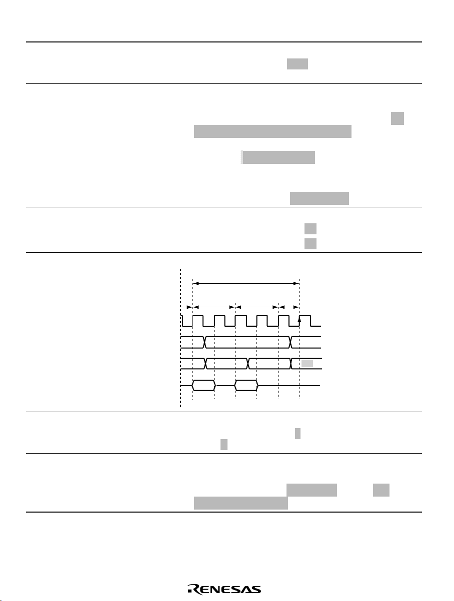
[3]
[4] IRTR = 0
[6] IRIC clearance
Bit 7
[3]
A
[4] IRTR = 1 [13] IRTR = 1[13] IRTR = 0
[9] TRS set to 1
[7] ACKB set to 1
666 Description amended
(5) Read ICDR and clear the IRIC flag in ICCR to 0. The
RDRF flag is cleared to 0.
Bit 6 Bit 5 Bit 4 Bit 3 Bit 2 Bit 1 Bit 0Bit 0
[11] IRIC clearance
[10] ICDR read (data 2)
Read the IRDR flag and clear the
IRIC flag to 0 consecutively, with no interrupt processing
occurring between them. If the time needed to transmit one
byte of data elapses before the IRIC flag is cleared, it will not
be possible to determine when the transfer has completed.
Figure 16.15 Example of
Slave Receive Mode
667 Description of "Interrupt request generation" deleted from
figure 16.15
Operation Timing (1) (MLS =
ACKB = 0)
Figure 16.16 Example of
Slave Receive Mode
668 Description of "Interrupt request generation" deleted from
figure 16.16
Operation Timing (2) (MLS =
ACKB = 0)
[12] [12]
A
[14] IRIC clearance
[15] WAIT cleared to 0
IRIC clearance
Stop condition
generated
Data 3Data 2Data 1
[17] Stop condition
issued
[16] ICDR read (data 3)
Rev. 5.00 Aug 08, 2006 page xxxvi of lxxxvi
Page 37

Item Page Revision (See Manual for Details)
16.4.6 Slave Transmit
Operation
Figure 16.18 Example of
669 to
Section 16.4.6 description replaced
671
671 Figure 16.18 replaced
Slave Transmit Mode
Operation Timing (MLS = 0)
16.4.8 Operation Using the
DTC
Table 16.5 Flags and
Transfer States
673 Table 16.5 amended
Item
Slave address +
R/W bit
Transmission/
reception
Dummy data
read
Actual data
transmission/rec
eption
Master Transmit
Mode
Transmission by
DTC (ICDR write)
Processing by
Transmission by
DTC (ICDR write)
Master Receive
Mode
Transmission by
CPU (ICDR write)
CPU (ICDR read)
Reception by
DTC (ICDR read)
16.6 Usage Notes 676 Description amended
1. ... the start condition, read
PORT in each I2C bus output
pin, and check that SCL and SDA are both low.
ICE bit is set to 1, it is possible to monitor the pin state by
reading the PORT register so long as the DDR I/O port
register corresponding to the pin has been cleared to 0.Then
issue the instruction ...
2. Either of ...
Read access to ICDR when ICE = 1 and TRS = 0
(including automatic transfer from IC
Table 16.8 Permissible SCL
Rise Time (t
) Values
sr
678 Note *2 added to table 16.8
φ = 5 MHz
2
*
φ = 8 MHz
2
*
φ = 16 MHz
Note 2 added
Notes: 1. Supported only by the H8S/2239 Group.
2. The H8S/2258 Group is out of operation.
Table 16.9 I2C Bus Timing
(with Maximum Influence of
tSr/tSf)
679 Note *7 added to table 16.9
φ = 5 MHz
7
*
φ = 8 MHz
7
*
680 Note 7 added
7. The H8S/2258 Group is out of operation.
Note:
Figure 16.22 Flowchart and
Timing of Start Condition
Instruction Issuance for
Retransmission
681 Figure 16.22 amended
(Before) [2] Determine whether SCL
Determine whether SCL is low
Slave Transmit
Mode
Reception by CPU
(ICDR read)
Transmission by
DTC (ICDR write)
Slave Receive
Mode
Reception by CPU
(ICDR read)
Reception by DTC
(ICDR read)
Even if the
DRS to ICDRR)
1
*
φ = 20 MHz
1
*
0 is low → (After)
Rev. 5.00 Aug 08, 2006 page xxxvii of lxxxvi
Page 38

Item Page Revision (See Manual for Details)
16.6 Usage Notes
Figure 16.26 TRS Bit
684 Figure 16.26 amended
TRS bit
Setting Timing in Slave Mode
686,
687
Description of "16. Notes on Wait Operation in Master
Mode" added
17.1 Features 689 Description added
• Selectable range voltages of analog inputs
The range of voltages of analog inputs to be converted can
be specified using the V
signal as the analog reference
ref
voltage.
Figure 17.1 Block Diagram
690 Figure 17.1 amended
of A/D Converter
AV
CC
Vref
10-
AV
SS
AN0
AN1
AN2
AN3
AN4
AN5
AN6
AN7
Multiplexer
17.4 Interface to Bus Master 696 Section 17.4 description added
18.1 Features 707 "• D/A output retaining function in software standby mode"
deleted
18.5.1 Analog Power Supply
Current in
Power-Down Mode
20.1 Features
Figure 20.1 Block Diagram
711 Section 18.5.1 description replaced
716 Figure 20.1 amended
H8S/22
27: 128 kbytes
of Flash Memory
20.3 Block Configuration
Figure 20.6 Block
722 Figure 20.6 amended
EB10 Erase unit
64 kbytes
Configuration of 256-kbyte
Flash Memory
Rev. 5.00 Aug 08, 2006 page xxxviii of lxxxvi
Page 39
Item Page Revision (See Manual for Details)
20.8.2 Erase/Erase-Verify
Figure 20.12 Erase/EraseVerify Flowchart
741 Figure 20.12 amended
tse: Wait 10 ms*
5
n≥100?*
Note 5 added
5. This is a recommended value. To change it, consult
Note:
5
tables 27.12, 27.25, 27.37, 27.49, and 27.59 and select a
new value such that the erase time (tE), wait time after E1 bit
setting (tse), and maximum erase count (N) do not exceed
the maximum values indicated.
20.11 Programmer Mode
Figure 20.13 Socket
Adapter Pin Correspondence
Diagram
744 Figure 20.13 amended
3
*
FP-100B
TFP-100G
Notes amended
4
*
TBP-112A
Notes: 1. Supported only by the H8S/
2. Supported only by the H8S/2238R.
3. Not supported by the H8S/2227.
4. Not supported by the H8S/2258.
5. Supported only by the H8S/2238R and H8S/2239.
20.13 Flash Memory
Programming and Erasing
Precautions
748 Figure 20.14 amended
MD2
to MD0*
1
Figure 20.14 Power-On/Off
Timing (Boot Mode)
Figure 20.15 Power-On/Off
Timing (User Program Mode)
Figure 20.16 Mode
Transition Timing (Example:
Boot Mode →User
749 Figure 20.15 amended
MD2
to MD0*
1
750 Figure 20.16 amended
to MD0
MD2
Mode↔User Program Mode)
21.1 Features 753
• Size
HD6432236BW and HD6432238RW added
Product Class ROM Size ROM Address (Modes 6 and 7)
H8S/2238 Group HD6432238B 256 kbytes H'000000 to H'03FFFF
HD6432236B 128 kbytes H'000000 to H'01FFFF
HD6432238R 256 kbytes H'000000 to H'03FFFF
HD6432236R 128 kbytes H'000000 to H'01FFFF
HD6432238BW 256 kbytes H'000000 to H'03FFFF
HD6432236BW 128 kbytes H'000000 to H'01FFFF
HD6432238RW 256 kbytes H'000000 to H'03FFFF
HD6432236RW 128 kbytes H'000000 to H'03FFFF
5
*
2258 and H8S/2238B.
Rev. 5.00 Aug 08, 2006 page xxxix of lxxxvi
Page 40

Item Page Revision (See Manual for Details)
22.3.1 Programming and
Verification
760 Figure 22.4 amended
Program width t
OPW
= 0.2n ms
Figure 22.4 High-Speed
Programming Flowchart
23.1.2 Low-Power Control
Register (LPWRCR)
23.2.1 Connecting a Crystal
Resonator
768 DTON description amended
Transfer ON Flag
Direct
771 Note 1 amended
Note: 1.
The H8S/2258 Group is out of operation.
Table 23.1 Damping
Resistance Value
Table 23.2 Crystal
Resonator Characteristics
771 Note 1 amended
Note: 1.
The H8S/2258 Group is out of operation.
23.2.2 External Clock Input Table of "External Clock Input Conditions (2) (H8S/2238
Group, H8S/2237 Group, H8S/2227 Group)" deleted
Table 23.3 External Clock
Input Conditions (2)
773,
774
Tables 23.3 (2) to (4) added
(H8S/2238B, H8S/2236B)
Table 23.3 External Clock
Input Conditions (3)
(H8S/2238R, H8S/2236R)
Table 23.3 External Clock
Input Conditions (4)
(H8S/2237 Group, H8S/2227
Group)
Table 23.3 External Clock
Input Conditions (
5)
774 Table title amended
(H8S/2239 Group)
23.2.2 External Clock Input
Table 23.4 External Clock
Input Conditions (Duty
Adjustment Circuit Unused)
(1) (H8S/2258 Group)
775 Note added
Note: If the duty adjustment circuit is not used, maximum
operating frequency is lowered according to the input
waveform. (Example: t
clock cycle time = 88 ns, and maximum operating frequency
EXL
= t
= 37 ns, t
EXH
EXr
= t
= 7 ns,
EXf
= 11.3 MHz)
Table of "External Clock Input Conditions (Duty Adjustment
Circuit Unused) (2) (H8S/2238 Group, H8S/2237 Group,
H8S/2227 Group)" deleted
Rev. 5.00 Aug 08, 2006 page xl of lxxxvi
Page 41

Item Page Revision (See Manual for Details)
23.2.2 External Clock Input
Table 23.4 External Clock
775,
776
Tables 23.4 (2) to (4) added
Input Conditions (Duty
Adjustment Circuit Unused)
(2) (H8S/2238B, H8S/2236B)
Table 23.4 External Clock
Input Conditions (Duty
Adjustment Circuit Unused)
(3) (H8S/2238R, H8S/2236R)
Table 23.4 External Clock
Input Conditions (Duty
Adjustment Circuit Unused)
(4) (H8S/2237 Group,
H8S/2227 Group)
Table 23.4 External Clock
Input Conditions (Duty
Adjustment Circuit Unused)
5) (H8S/2239 Group)
(
23.2.3 Notes on Switching
External Clock
Figure 23.7 External Clock
777 Note amended
Note: When a duty adjustment circuit is not used, maximum
operating frequency is lowered according to the input
waveform. (Example: t
clock cycle time =
=
16.6 MHz)
60 ns, and maximum operating frequency
778 Figure 23.7 amended
clock φ
External
interrupt
EXL
= t
= 25 ns, t
EXH
200 ns or more
Switching Timing (Example)
23.7.1 Connecting 32.768kHz Crystal Resonator
780 Figure 23.9 amended
Rs = 14
kΩ (typ)
Figure 23.9 Equivalence
Circuit for 32.768-kHz
Oscillator
23.7.2 Handling Pins when
Subclock Not Required
781 Description amended
... LPWRCR must be set to 1.
If the SUBSTP bit is not set to
1, transitions to the power-down modes may not complete
normally.
Section 24 Power-Down
Mode
Table 24.1 LSI Internal
States in Each Mode
784,
785
Note *5 added to table 24.1
5
*3*
D/A
Note 5 added
5. The analog output value does not satisfy the
Note:
specified D/A absolute accuracy when D/A is halted
(retained). However, the H8S/2258 Group, H8S/2238B, and
H8S/2236B satisfy the specified D/A absolute accuracy.
= t
EXr
standby time
(4)
= 5 ns,
EXf
Active (External clock 1)Active (External clock 2) Software standby mode
Rev. 5.00 Aug 08, 2006 page xli of lxxxvi
Page 42

Item Page Revision (See Manual for Details)
24.1.2 Module Stop Control
Registers A to C (MSTPCRA
to MSTPCRC)
789
• MSTPCRA
Target module description of MSTPA0 amended
8-bit timer (TMR_2
3
*
, TMR_3
3
*
)
• MSTPCRB
Target module description of MSTPB5 amended
2 (SCI_2
790
Serial communication interface
• MSTPCRC
Bit 3 description amended
5
*1*
(Before) MSTPC3
→ (After) MSTPC3
(Before) IEBus controller → (After) IEBus controller
Notes 3 and 4 amended
Notes: 3.
Not available in the H8S/2237 Group and
H8S/2227 Group.
Not available in the H8S/2227 Group.
4.
790 Description amended
... The bus masters other than the CPU (DMAC* and DTC)...
24.2 Medium-Speed Mode 791 Notes * added
Note: * Supported only by the H8S/2239 Group.
24.4.3 Oscillation Settling
Time after Clearing Software
Standby Mode
Table 24.3 Oscillation
Settling Time Settings
793 Table 24.3 amended
STS2 STS1 STS0 Standby Time
0 0 0 8192 states 1. 4 2.0 4.1 ms
1 16384 states 2.7 4.1 8.2
1 0 32768 states 5.5 8.2 16.4
1 65536 states 10.9 16.4 32.8
1 0 0 131072 states 21.8 32.8 65.5
1 262144 states 43.7 65.5 131.1
10Reserved
1 16 states 2.7 4.0 8.0 µ s
6
MHz
4
2
2
*
*
MHz
2
MHz
4
*
)
5
*
2
*
Unit
Notes 1 and 2 amended
Notes: 1. Supported only by the H8S/22
The H8S/2258 Group is out of operation.
2.
24.6 Module Stop Mode 796 Note * added
*
DMAC
Note: * Supported only by the H8S/2239 Group only.
Rev. 5.00 Aug 08, 2006 page xlii of lxxxvi
39 Group.
Page 43

Item Page Revision (See Manual for Details)
24.12.4 On-Chip Module
Interrupt
801
• Module Stop Mode
• Subactive Mode/Watch Mode
Note *2 added
1
2
*
*
DMAC
IIC
Notes: 1. Supported only by the H8S/2239 Group.
2. Not available in the H8S/2237 Group and H8S/2227
Group.
26.3 Register States in Each
Operating Mode
27.1 Power Supply Voltage
837 Table amended
Register
Name Reset
ICDR_0 Initialized Initialized Initialized IIC_0
SARX_0 Initialized Initialized Initialized
ICMR_0 Initialized Initialized Initialized
SAR_0 Initialized Initialized
Manual
Reset
Highspeed
Mediumspeed Sleep
841 Figure 27.3 title amended
Module
Stop Watch
and Operating Frequency
Range
Figure 27.3 Power Supply
Voltage and Operating
Frequency Ranges
H8S/2238B and H8S/2236B)
(
Figure 27.4 Power Supply
842 Figure 27.4 title amended
Voltage and Operating
Frequency Ranges
(H8S/2238R
and H8S/2236R)
Subactive
Subsleep
Software
Hardware
Standby
Standby Module
Initialized
Rev. 5.00 Aug 08, 2006 page xliii of lxxxvi
Page 44
Item Page Revision (See Manual for Details)
27.2.2 DC Characteristics
Table 27.2 DC
Characteristics (1)
845,
846
Table 27.2 amended
Item Symbol
Input high
voltage
Input low
voltage
Input
leakage
current
RES, STBY,
NMI, MD2 to
MD0, FWE
EXTAL, Ports
1, 3, 7, and A
to G
Ports 4 and 9
RES, STBY,
MD2 to MD0,
FWE
NMI, EXTAL,
Ports 1, 3, 4,
7, 9, and A to
G
RES
STBY, NMI,
MD2 to MD0,
FWE
Ports 4 and 9
V
V
| Iin |
IH
IL
27.2.6 Flash Memory
Characteristics
Table 27.12 Flash Memory
Characteristics
27.3.2 DC Characteristics
Table 27.14 DC
Characteristics (2)
Table 27.14 DC
Characteristics (3)
27.3.5 D/A Conversion
Characteristics
Table 27.24 D/A Conversion
Characteristics
27.3.6 Flash Memory
Characteristics
Table 27.25 Flash Memory
Characteristics
863 Note 7 amended
Note: 7. Reference value at 25°C.
reference that rewriting is enabled up to this value.)
868 Note 3 amended
Note: 3. The values are for V
– 0.2, and VIL max = 0.2 V.
V
CC
870 Note 3 amended
Note: 3. The values are for V
– 0.2, and VIL max = 0.2 V.
V
CC
884 Table 27.24 amended
Absolute accuracy
*
Note: * Does not apply in module stop mode, software
standby mode, watch mode, subactive mode, or subsleep
mode.
885 Table 27.25 amended
Item Symbol Min Typ Max Unit
Programming time
Erase time
Reprogramming count N
Data hold time
1*2*4
*
1*3*5
*
8
*
(Normally, it is a
≤ VCC < 2.7 V, VIH min =
RAM
≤ VCC < 2.2 V, VIH min =
RAM
t
10 200 ms/128 bytes
P
t
100 1200 ms/block
E
t
DRP
6
*
100
WEC
10000
10 year
*
7
Times
Test
Conditions
Rev. 5.00 Aug 08, 2006 page xliv of lxxxvi
Page 45

Item Page Revision (See Manual for Details)
27.3.6 Flash Memory
Characteristics
Table 27.25 Flash Memory
Characteristics
886 Notes 6 and 7 amended, note 8 added
Notes: 6. The minimum times that all characteristics after
rewriting are guaranteed. (A range between 1 and minimum
value is guaranteed.)
The reference value at 25°C. (Normally, it is a reference
7.
that rewriting is enabled up to this value.)
8. Data hold characteristics when rewriting is performed
within the range of specifications including minimum value.
27.4 Electrical
Characteristics
of H8S/2238B
887 Section 27.4 title amended
and H8S/2236B
27.4.2 DC Characteristics
Table 27.27 DC
Characteristics (1)
27.4.6 Flash Memory
Characteristics
Table 27.37 Flash Memory
Characteristics
889 Note 2 amended
Note: 2. In order to output high
must be connected externally.
905 Table 27.37 amended
Item Symbol Min Typ Max Unit
Programming time
Erase time
Rewrite times N
Data holding time
*
1*3*5
1*2*4
*
8
*
level, a pull-up resistance
t
P
t
E
WEC
t
DRP
906 Notes 6 and 7 amended, note 8 added
Notes: 6.
The minimum times that all characteristics after
rewriting are guaranteed. (A range between 1 and minimum
value is guaranteed.)
The reference value at 25°C. (Normally, it is a reference
7.
that rewriting is enabled up to this value.)
8. Data hold characteristics when rewriting is performed
within the range of specifications including minimum value.
27.5.5 D/A Conversion
Characteristics
Table 27.48 D/A Conversion
Characteristics
924 Table 27.48 amended
Absolute accuracy
*
Note * added
Note: * Does not apply in module stop mode, software
standby mode, watch mode, subactive mode, or subsleep
mode.
27.5.6 Flash Memory
Characteristics
Table 27.49 Flash Memory
Characteristics
925 Table 27.49 amended
Item Symbol Min Typ Max Unit
Programming time
Erase time
Reprogramming count N
Data holding time t
*
1*3*5
1*2*4
*
8
*
t
10 200 ms/128 bytes
P
t
100 1200 ms/block
E
WEC
DRP
6
*
100 10000
10 year
10 200 ms/
100 1200 ms/block
6
*
100
10000
10 Years
7
*
Times
7
*
Times
128 bytes
Test
Conditions
Test
Conditions
Rev. 5.00 Aug 08, 2006 page xlv of lxxxvi
Page 46

Item Page Revision (See Manual for Details)
27.5.6 Flash Memory
Characteristics
Table 27.49 Flash Memory
Characteristics
926 Notes 6 and 7 amended, note 8 added
Notes: 6. The minimum times that all characteristics after
rewriting are guaranteed. (A range between 1 and minimum
value is guaranteed.)
The reference value at 25°C. (Normally, it is a reference
7.
that rewriting is enabled up to this value.)
8. Data hold characteristics when rewriting is performed
within the range of specifications including minimum value.
27.6.2 DC Characteristics
Table 27.52 Permissible
936 Table 27.52 amended
Conditions (
ZTAT version and F-ZTAT version):
Output Currents
27.6.5 D/A Conversion
Characteristics
Table 27.58 D/A Conversion
Characteristics
945 Table 27.58 amended
Absolute accuracy
*
Note: * Does not apply in module stop mode, software
standby mode, watch mode, subactive mode, or subsleep
mode.
27.6.6 Flash Memory
Characteristics
Table 27.59 Flash Memory
Characteristics
946 Table 27.59 amended
Item Symbol Min Typ Max Unit
Programming time
Erase time
Reprogramming count N
Data holding time
*
1*3*5
1*2*4
*
8
*
tP 10 200 ms/128 bytes
tE 100 1200 ms/block
t
DRP
6
*
100
WEC
10000
10 year
947 Notes 6 and 7 amended, note 8 added
Notes: 6.
The minimum times that all characteristics after
rewriting are guaranteed. (A range between 1 and minimum
value is guaranteed.)
The reference value at 25°C. (Normally, it is a reference
7.
that rewriting is enabled up to this value.)
8. Data hold characteristics when rewriting is performed
within the range of specifications including minimum value.
A.1 I/O Port State in Each
Pin State
967 Note 2 amended
Note: 2.
Not available in the H8S/2237 Group and
H8S/2227 Group.
7
*
Times
Test
Conditions
Rev. 5.00 Aug 08, 2006 page xlvi of lxxxvi
Page 47

Contents
Section 1 Overview............................................................................................................. 1
1.1 Features ............................................................................................................................. 1
1.2 Internal Block Diagram..................................................................................................... 4
1.3 Pin Description.................................................................................................................. 9
1.3.1 Pin Arrangement .................................................................................................. 9
1.3.2 Pin Arrangements in Each Mode ......................................................................... 20
1.3.3 Pin Functions ....................................................................................................... 44
Section 2 CPU ...................................................................................................................... 63
2.1 Features ............................................................................................................................. 63
2.1.1 Differences between H8S/2600 CPU and H8S/2000 CPU .................................. 64
2.1.2 Differences from H8/300 CPU ............................................................................ 65
2.1.3 Differences from H8/300H CPU.......................................................................... 65
2.2 CPU Operating Modes ...................................................................................................... 66
2.2.1 Normal Mode ....................................................................................................... 66
2.2.2 Advanced Mode ................................................................................................... 67
2.3 Address Space ................................................................................................................... 70
2.4 Register Configuration ...................................................................................................... 71
2.4.1 General Registers ................................................................................................. 72
2.4.2 Program Counter (PC) ......................................................................................... 73
2.4.3 Extended Control Register (EXR) ....................................................................... 73
2.4.4 Condition-Code Register (CCR) .......................................................................... 74
2.4.5 Initial Values of CPU Registers ........................................................................... 75
2.5 Data Formats..................................................................................................................... 76
2.5.1 General Register Data Formats ............................................................................ 76
2.5.2 Memory Data Formats ......................................................................................... 78
2.6 Instruction Set ................................................................................................................... 79
2.6.1 Table of Instructions Classified by Function ....................................................... 80
2.6.2 Basic Instruction Formats .................................................................................... 89
2.7 Addressing Modes and Effective Address Calculation ..................................................... 90
2.7.1 Register Direct—Rn............................................................................................. 91
2.7.2 Register Indirect—@ERn .................................................................................... 91
2.7.3 Register Indirect with Displacement—@(d:16, ERn) or @(d:32, ERn).............. 91
2.7.4 Register Indirect with Post-Increment—@ERn+ or Register Indirect
with Pre-Decrement—@-ERn ............................................................................. 91
2.7.5 Absolute Address—@aa:8, @aa:16, @aa:24, or @aa:32.................................... 91
2.7.6 Immediate—#xx:8, #xx:16, or #xx:32 ................................................................. 92
Rev. 5.00 Aug 08, 2006 page xlvii of lxxxvi
Page 48

2.7.7 Program-Counter Relative—@(d:8, PC) or @(d:16, PC).................................... 92
2.7.8 Memory Indirect—@@aa:8 ................................................................................ 93
2.7.9 Effective Address Calculation ............................................................................. 94
2.8 Processing States............................................................................................................... 96
2.9 Usage Notes ...................................................................................................................... 98
2.9.1 TAS Instruction.................................................................................................... 98
2.9.2 STM/LDM Instruction......................................................................................... 98
2.9.3 Bit Manipulation Instructions .............................................................................. 98
2.9.4 Access Methods for Registers with Write-Only Bits ........................................... 100
Section 3 MCU Operating Modes .................................................................................. 103
3.1 Operating Mode Selection................................................................................................. 103
3.2 Register Descriptions ........................................................................................................ 104
3.2.1 Mode Control Register (MDCR) ......................................................................... 104
3.2.2 System Control Register (SYSCR)...................................................................... 105
3.3 Operating Mode Descriptions ........................................................................................... 106
3.3.1 Mode 4 ................................................................................................................. 106
3.3.2 Mode 5 ................................................................................................................. 106
3.3.3 Mode 6 ................................................................................................................. 107
3.3.4 Mode 7 ................................................................................................................. 107
3.3.5 Pin Functions ....................................................................................................... 108
3.4 Memory Map in Each Operating Mode ............................................................................ 109
Section 4 Exception Handling ......................................................................................... 119
4.1 Exception Handling Types and Priority ............................................................................ 119
4.2 Exception Sources and Exception Vector Table ............................................................... 119
4.3 Reset 121
4.3.1 Reset Types.......................................................................................................... 121
4.3.2 Reset Exception Handling.................................................................................... 122
4.3.3 Interrupts after Reset............................................................................................ 123
4.3.4 State of On-Chip Peripheral Modules after Reset Release................................... 123
4.4 Traces................................................................................................................................ 123
4.5 Interrupts ........................................................................................................................... 124
4.6 Trap Instruction................................................................................................................. 124
4.7 Stack Status after Exception Handling.............................................................................. 125
4.8 Usage Note........................................................................................................................ 126
Section 5 Interrupt Controller .......................................................................................... 127
5.1 Features ............................................................................................................................. 127
5.2 Input/Output Pins .............................................................................................................. 129
Rev. 5.00 Aug 08, 2006 page xlviii of lxxxvi
Page 49

5.3 Register Descriptions ........................................................................................................ 129
5.3.1 Interrupt Priority Registers A to L, and O (IPRA to IPRL, IPRO) ...................... 130
5.3.2 IRQ Enable Register (IER) .................................................................................. 131
5.3.3 IRQ Sense Control Registers H and L (ISCRH and ISCRL) ............................... 131
5.3.4 IRQ Status Register (ISR).................................................................................... 134
5.4 Interrupt Sources ............................................................................................................... 135
5.4.1 External Interrupts................................................................................................ 135
5.4.2 Internal Interrupts................................................................................................. 136
5.4.3 Interrupt Exception Handling Vector Table......................................................... 136
5.5 Operation........................................................................................................................... 142
5.5.1 Interrupt Control Modes and Interrupt Operation ................................................ 142
5.5.2 Interrupt Control Mode 0 ..................................................................................... 145
5.5.3 Interrupt Control Mode 2 ..................................................................................... 147
5.5.4 Interrupt Exception Handling Sequence .............................................................. 148
5.5.5 Interrupt Response Times .................................................................................... 150
5.5.6 DTC and DMAC Activation by Interrupt ............................................................ 151
5.6 Usage Notes ...................................................................................................................... 154
5.6.1 Contention between Interrupt Generation and Disabling..................................... 154
5.6.2 Instructions that Disable Interrupts ...................................................................... 155
5.6.3 When Interrupts are Disabled............................................................................... 155
5.6.4 Interrupts during Execution of EEPMOV Instruction.......................................... 155
Section 6 PC Break Controller (PBC) ........................................................................... 157
6.1 Features ............................................................................................................................. 157
6.2 Register Descriptions ........................................................................................................ 158
6.2.1 Break Address Register A (BARA) ..................................................................... 158
6.2.2 Break Address Register B (BARB)...................................................................... 159
6.2.3 Break Control Register A (BCRA) ...................................................................... 159
6.2.4 Break Control Register B (BCRB)....................................................................... 160
6.3 Operation........................................................................................................................... 160
6.3.1 PC Break Interrupt Due to Instruction Fetch........................................................ 160
6.3.2 PC Break Interrupt Due to Data Access............................................................... 161
6.3.3 Notes on PC Break Interrupt Handling ................................................................ 161
6.3.4 Operation in Transitions to Power-Down Modes................................................. 161
6.3.5 When Instruction Execution Is Delayed by One State......................................... 162
6.4 Usage Notes ...................................................................................................................... 163
6.4.1 Module Stop Mode Setting .................................................................................. 163
6.4.2 PC Break Interrupts.............................................................................................. 163
6.4.3 CMFA and CMFB ............................................................................................... 163
6.4.4 PC Break Interrupt when DTC and DMAC Is Bus Master.................................. 163
Rev. 5.00 Aug 08, 2006 page xlix of lxxxvi
Page 50

6.4.5 PC Break Set for Instruction Fetch at Address Following BSR, JSR, JMP,
TRAPA, RTE, and RTS Instruction..................................................................... 163
6.4.6 I Bit Set by LDC, ANDC, ORC, and XORC Instruction..................................... 164
6.4.7 PC Break Set for Instruction Fetch at Address Following Bcc Instruction.......... 164
6.4.8 PC Break Set for Instruction Fetch at Branch Destination Address of Bcc
Instruction ............................................................................................................ 164
Section 7 Bus Controller ................................................................................................... 165
7.1 Features ............................................................................................................................. 165
7.2 Input/Output Pins .............................................................................................................. 167
7.3 Register Descriptions ........................................................................................................ 167
7.3.1 Bus Width Control Register (ABWCR)............................................................... 168
7.3.2 Access State Control Register (ASTCR) ............................................................. 168
7.3.3 Wait Control Registers H and L (WCRH, WCRL).............................................. 169
7.3.4 Bus Control Register H (BCRH) ......................................................................... 172
7.3.5 Bus Control Register L (BCRL) .......................................................................... 173
7.3.6 Pin Function Control Register (PFCR) ................................................................ 174
7.4 Bus Control....................................................................................................................... 175
7.4.1 Area Divisions ..................................................................................................... 175
7.4.2 Bus Specifications................................................................................................ 176
7.4.3 Bus Interface for Each Area................................................................................. 177
7.4.4 Chip Select Signals .............................................................................................. 178
7.5 Basic Timing..................................................................................................................... 178
7.5.1 On-Chip Memory (ROM, RAM) Access Timing ................................................ 179
7.5.2 On-Chip Peripheral Module Access Timing........................................................ 180
7.5.3 External Address Space Access Timing .............................................................. 181
7.6 Basic Bus Interface ........................................................................................................... 181
7.6.1 Data Size and Data Alignment............................................................................. 181
7.6.2 Valid Strobes........................................................................................................ 182
7.6.3 Basic Timing........................................................................................................ 183
7.6.4 Wait Control ........................................................................................................ 190
7.7 Burst ROM Interface......................................................................................................... 192
7.7.1 Basic Timing........................................................................................................ 192
7.7.2 Wait Control ........................................................................................................ 194
7.8 Idle Cycle .......................................................................................................................... 194
7.9 Bus Release....................................................................................................................... 197
7.9.1 Bus Release Usage Note ...................................................................................... 198
7.10 Bus Arbitration.................................................................................................................. 199
7.10.1 Operation ............................................................................................................. 199
7.10.2 Bus Transfer Timing............................................................................................ 200
Rev. 5.00 Aug 08, 2006 page l of lxxxvi
Page 51

7.10.3 External Bus Release Usage Note........................................................................ 200
7.11 Resets and the Bus Controller ........................................................................................... 201
Section 8 DMA Controller (DMAC) ............................................................................. 203
8.1 Features ............................................................................................................................. 203
8.2 Input/Output Pins .............................................................................................................. 205
8.3 Register Descriptions ........................................................................................................ 205
8.3.1 Memory Address Registers (MARA and MARB)............................................... 207
8.3.2 I/O Address Registers (IOARA and IOARB) ...................................................... 207
8.3.3 Execute Transfer Count Registers (ETCRA and ETCRB)................................... 208
8.3.4 DMA Control Registers (DMACRA and DMACRB) ......................................... 209
8.3.5 DMA Band Control Registers H and L (DMABCRH and DMABCRL)............. 218
8.3.6 DMA Write Enable Register (DMAWER) .......................................................... 229
8.3.7 DMA Terminal Control Register (DMATCR)..................................................... 231
8.4 Activation Sources ............................................................................................................ 231
8.4.1 Activation by Internal Interrupt Request.............................................................. 232
8.4.2 Activation by External Request ........................................................................... 233
8.4.3 Activation by Auto-Request................................................................................. 233
8.5 Operation........................................................................................................................... 234
8.5.1 Transfer Modes .................................................................................................... 234
8.5.2 Sequential Mode .................................................................................................. 236
8.5.3 Idle Mode ............................................................................................................. 239
8.5.4 Repeat Mode ........................................................................................................ 241
8.5.5 Single Address Mode........................................................................................... 244
8.5.6 Normal Mode ....................................................................................................... 248
8.5.7 Block Transfer Mode ........................................................................................... 251
8.5.8 Basic Bus Cycles.................................................................................................. 256
8.5.9 DMA Transfer (Dual Address Mode) Bus Cycles ............................................... 257
8.5.10 DMA Transfer (Single Address Mode) Bus Cycles............................................. 265
8.5.11 Multi-Channel Operation ..................................................................................... 271
8.5.12 Relation between DMAC and External Bus Requests, and DTC ........................ 272
8.5.13 DMAC and NMI Interrupts.................................................................................. 272
8.5.14 Forced Termination of DMAC Operation............................................................ 273
8.5.15 Clearing Full Address Mode ................................................................................ 274
8.6 Interrupt Sources ............................................................................................................... 275
8.7 Usage Notes ...................................................................................................................... 276
8.7.1 DMAC Register Access during Operation........................................................... 276
8.7.2 Module Stop......................................................................................................... 277
8.7.3 Medium-Speed Mode........................................................................................... 277
8.7.4 Activation by Falling Edge on DREQ Pin ........................................................... 278
Rev. 5.00 Aug 08, 2006 page li of lxxxvi
Page 52

8.7.5 Activation Source Acceptance ............................................................................. 278
8.7.6 Internal Interrupt after End of Transfer................................................................ 278
8.7.7 Channel Re-Setting .............................................................................................. 279
Section 9 Data Transfer Controller (DTC)................................................................... 281
9.1 Features ............................................................................................................................. 281
9.2 Register Descriptions ........................................................................................................ 282
9.2.1 DTC Mode Register A (MRA) ............................................................................ 283
9.2.2 DTC Mode Register B (MRB)............................................................................. 285
9.2.3 DTC Source Address Register (SAR).................................................................. 285
9.2.4 DTC Destination Address Register (DAR).......................................................... 285
9.2.5 DTC Transfer Count Register A (CRA) .............................................................. 286
9.2.6 DTC Transfer Count Register B (CRB)............................................................... 286
9.2.7 DTC Enable Registers A to G, and I (DTCERA to DTCERG, and DTCERI) .... 286
9.2.8 DTC Vector Register (DTVECR)........................................................................ 288
9.3 Activation Sources ............................................................................................................ 289
9.4 Location of Register Information and DTC Vector Table ................................................ 290
9.5 Operation .......................................................................................................................... 294
9.5.1 Normal Mode ....................................................................................................... 295
9.5.2 Repeat Mode ........................................................................................................ 295
9.5.3 Block Transfer Mode........................................................................................... 296
9.5.4 Chain Transfer ..................................................................................................... 298
9.5.5 Interrupts .............................................................................................................. 299
9.5.6 Operation Timing................................................................................................. 299
9.5.7 Number of DTC Execution States........................................................................ 301
9.6 Procedures for Using DTC................................................................................................ 302
9.6.1 Activation by Interrupt......................................................................................... 302
9.6.2 Activation by Software ........................................................................................ 302
9.7 Examples of Use of the DTC ............................................................................................ 303
9.7.1 Normal Mode ....................................................................................................... 303
9.7.2 Software Activation ............................................................................................. 303
9.8 Usage Notes ...................................................................................................................... 304
9.8.1 Module Stop Mode Setting .................................................................................. 304
9.8.2 On-Chip RAM ..................................................................................................... 304
9.8.3 DTCE Bit Setting................................................................................................. 304
Section 10 I/O Ports............................................................................................................ 305
10.1 Port 1................................................................................................................................. 309
10.1.1 Port 1 Data Direction Register (P1DDR)............................................................. 309
10.1.2 Port 1 Data Register (P1DR)................................................................................ 310
Rev. 5.00 Aug 08, 2006 page lii of lxxxvi
Page 53

10.1.3 Port 1 Register (PORT1)...................................................................................... 310
10.1.4 Pin Functions ....................................................................................................... 311
10.2 Port 3................................................................................................................................. 315
10.2.1 Port 3 Data Direction Register (P3DDR)............................................................. 315
10.2.2 Port 3 Data Register (P3DR)................................................................................ 316
10.2.3 Port 3 Register (PORT3)...................................................................................... 316
10.2.4 Port 3 Open Drain Control Register (P3ODR)..................................................... 317
10.2.5 Pin Functions ....................................................................................................... 317
10.3 Port 4................................................................................................................................. 321
10.3.1 Port 4 Register (PORT4)...................................................................................... 321
10.3.2 Pin Functions ....................................................................................................... 321
10.4 Port 7................................................................................................................................. 322
10.4.1 Port 7 Data Direction Register (P7DDR)............................................................. 322
10.4.2 Port 7 Data Register (P7DR)................................................................................ 323
10.4.3 Port 7 Register (PORT7)...................................................................................... 323
10.4.4 Pin Functions ....................................................................................................... 324
10.5 Port 9................................................................................................................................. 327
10.5.1 Port 9 Register (PORT9)...................................................................................... 327
10.5.2 Pin Functions ....................................................................................................... 327
10.6 Port A................................................................................................................................ 328
10.6.1 Port A Data Direction Register (PADDR) ........................................................... 328
10.6.2 Port A Data Register (PADR).............................................................................. 328
10.6.3 Port A Register (PORTA) .................................................................................... 329
10.6.4 Port A Pull-Up MOS Control Register (PAPCR) ................................................ 329
10.6.5 Port A Open Drain Control Register (PAODR)................................................... 329
10.6.6 Pin Functions ....................................................................................................... 330
10.6.7 Input Pull-Up MOS States in Port A.................................................................... 332
10.7 Port B ................................................................................................................................ 332
10.7.1 Port B Data Direction Register (PBDDR)............................................................ 333
10.7.2 Port B Data Register (PBDR) .............................................................................. 333
10.7.3 Port B Register (PORTB) .................................................................................... 334
10.7.4 Port B Pull-Up MOS Control Register (PBPCR)................................................. 334
10.7.5 Pin Functions ....................................................................................................... 334
10.7.6 Input Pull-Up MOS States in Port B .................................................................... 339
10.8 Port C ................................................................................................................................ 339
10.8.1 Port C Data Direction Register (PCDDR)............................................................ 340
10.8.2 Port C Data Register (PCDR) .............................................................................. 340
10.8.3 Port C Register (PORTC) .................................................................................... 341
10.8.4 Port C Pull-Up MOS Control Register (PCPCR)................................................. 341
10.8.5 Pin Functions ....................................................................................................... 342
Rev. 5.00 Aug 08, 2006 page liii of lxxxvi
Page 54

10.8.6 Input Pull-Up MOS States in Port C.................................................................... 342
10.9 Port D................................................................................................................................ 343
10.9.1 Port D Data Direction Register (PDDDR) ........................................................... 343
10.9.2 Port D Data Register (PDDR).............................................................................. 344
10.9.3 Port D Register (PORTD).................................................................................... 344
10.9.4 Port D Pull-Up MOS Control Register (PDPCR) ................................................ 345
10.9.5 Pin Functions ....................................................................................................... 345
10.9.6 Input Pull-Up MOS States in Port D.................................................................... 346
10.10 Port E ................................................................................................................................ 346
10.10.1 Port E Data Direction Register (PEDDR)............................................................ 347
10.10.2 Port E Data Register (PEDR)............................................................................... 347
10.10.3 Port E Register (PORTE)..................................................................................... 348
10.10.4 Port E Pull-Up MOS Control Register (PEPCR)................................................. 348
10.10.5 Pin Functions ....................................................................................................... 349
10.10.6 Input Pull-Up MOS States in Port E .................................................................... 349
10.11 Port F ................................................................................................................................ 350
10.11.1 Port F Data Direction Register (PFDDR) ............................................................ 350
10.11.2 Port F Data Register (PFDR) ............................................................................... 351
10.11.3 Port F Register (PORTF) ..................................................................................... 351
10.11.4 Pin Functions ....................................................................................................... 352
10.12 Port G ................................................................................................................................ 354
10.12.1 Port G Data Direction Register (PGDDR) ........................................................... 354
10.12.2 Port G Data Register (PGDR).............................................................................. 355
10.12.3 Port G Register (PORTG).................................................................................... 355
10.12.4 Pin Functions ....................................................................................................... 355
Section 11 16-Bit Timer Pulse Unit (TPU).................................................................. 359
11.1 Features............................................................................................................................. 359
11.2 Input/Output Pins.............................................................................................................. 364
11.3 Register Descriptions........................................................................................................ 365
11.3.1 Timer Control Register (TCR)............................................................................. 367
11.3.2 Timer Mode Register (TMDR)............................................................................ 372
11.3.3 Timer I/O Control Register (TIOR) ..................................................................... 373
11.3.4 Timer Interrupt Enable Register (TIER).............................................................. 391
11.3.5 Timer Status Register (TSR)................................................................................ 393
11.3.6 Timer Counter (TCNT)........................................................................................ 396
11.3.7 Timer General Register (TGR) ............................................................................ 396
11.3.8 Timer Start Register (TSTR) ............................................................................... 396
11.3.9 Timer Synchronous Register (TSYR).................................................................. 397
11.4 Operation .......................................................................................................................... 398
Rev. 5.00 Aug 08, 2006 page liv of lxxxvi
Page 55

11.4.1 Basic Functions.................................................................................................... 398
11.4.2 Synchronous Operation........................................................................................ 403
11.4.3 Buffer Operation .................................................................................................. 405
11.4.4 Cascaded Operation ............................................................................................. 409
11.4.5 PWM Modes ........................................................................................................ 411
11.4.6 Phase Counting Mode .......................................................................................... 416
11.5 Interrupt Sources............................................................................................................... 423
11.6 DTC Activation................................................................................................................. 425
11.7 DMAC Activation (H8S/2239 Group Only)..................................................................... 425
11.8 A/D Converter Activation................................................................................................. 426
11.9 Operation Timing.............................................................................................................. 426
11.9.1 Input/Output Timing ............................................................................................ 426
11.9.2 Interrupt Signal Timing........................................................................................ 430
11.10 Usage Notes ...................................................................................................................... 433
11.10.1 Module Stop Mode Setting .................................................................................. 433
11.10.2 Input Clock Restrictions....................................................................................... 433
11.10.3 Caution on Cycle Setting ..................................................................................... 434
11.10.4 Contention between TCNT Write and Clear Operations ..................................... 434
11.10.5 Contention between TCNT Write and Increment Operations.............................. 435
11.10.6 Contention between TGR Write and Compare Match ......................................... 436
11.10.7 Contention between Buffer Register Write and Compare Match......................... 436
11.10.8 Contention between TGR Read and Input Capture.............................................. 437
11.10.9 Contention between TGR Write and Input Capture............................................. 438
11.10.10 Contention between Buffer Register Write and Input Capture ........................ 438
11.10.11 Contention between Overflow/Underflow and Counter Clearing.................... 439
11.10.12 Contention between TCNT Write and Overflow/Underflow........................... 440
11.10.13 Multiplexing of I/O Pins .................................................................................. 440
11.10.14 Interrupts and Module Stop Mode ................................................................... 440
Section 12 8-Bit Timers..................................................................................................... 441
12.1 Features............................................................................................................................. 441
12.2 Input/Output Pins.............................................................................................................. 443
12.3 Register Descriptions ........................................................................................................ 443
12.3.1 Timer Counter (TCNT)........................................................................................ 444
12.3.2 Time Constant Register A (TCORA)................................................................... 444
12.3.3 Time Constant Register B (TCORB) ................................................................... 445
12.3.4 Timer Control Register (TCR)............................................................................. 445
12.3.5 Timer Control/Status Register (TCSR)................................................................ 447
12.4 Operation........................................................................................................................... 452
12.4.1 Pulse Output......................................................................................................... 452
Rev. 5.00 Aug 08, 2006 page lv of lxxxvi
Page 56

12.5 Operation Timing.............................................................................................................. 453
12.5.1 TCNT Incrementation Timing ............................................................................. 453
12.5.2 Timing of CMFA and CMFB Setting when a Compare-Match Occurs............... 454
12.5.3 Timing of Timer Output when a Compare-Match Occurs................................... 455
12.5.4 Timing of Compare-Match Clear when a Compare-Match Occurs ..................... 455
12.5.5 TCNT External Reset Timing.............................................................................. 456
12.5.6 Timing of Overflow Flag (OVF) Setting ............................................................. 456
12.6 Operation with Cascaded Connection............................................................................... 457
12.6.1 16-Bit Count Mode .............................................................................................. 457
12.6.2 Compare-Match Count Mode .............................................................................. 457
12.7 Interrupt Sources............................................................................................................... 458
12.7.1 Interrupt Sources and DTC Activation ................................................................ 458
12.7.2 A/D Converter Activation.................................................................................... 458
12.8 Usage Notes ...................................................................................................................... 459
12.8.1 Contention between TCNT Write and Clear........................................................ 459
12.8.2 Contention between TCNT Write and Increment ................................................ 459
12.8.3 Contention between TCOR Write and Compare-Match ...................................... 460
12.8.4 Contention between Compare-Matches A and B................................................. 461
12.8.5 Switching of Internal Clocks and TCNT Operation............................................. 461
12.8.6 Contention between Interrupts and Module Stop Mode ...................................... 463
12.8.7 Mode Setting of Cascaded Connection................................................................ 463
Section 13 Watchdog Timer (WDT).............................................................................. 465
13.1 Features............................................................................................................................. 465
13.2 Input/Output Pins.............................................................................................................. 467
13.3 Register Descriptions........................................................................................................ 467
13.3.1 Timer Counter (TCNT)........................................................................................ 468
13.3.2 Timer Control/Status Register (TCSR)................................................................ 468
13.3.3 Reset Control/Status Register (RSTCSR) (only WDT_0) ................................... 472
13.4 Operation .......................................................................................................................... 473
13.4.1 Watchdog Timer Mode ........................................................................................ 473
13.4.2 Interval Timer Mode............................................................................................ 474
13.4.3 Timing of Setting Overflow Flag (OVF) ............................................................. 475
13.4.4 Timing of Setting Watchdog Timer Overflow Flag (WOVF) ............................. 476
13.5 Interrupt Sources............................................................................................................... 476
13.6 Usage Notes ...................................................................................................................... 477
13.6.1 Notes on Register Access..................................................................................... 477
13.6.2 Contention between Timer Counter (TCNT) Write and Increment..................... 478
13.6.3 Changing Value of CKS2 to CKS0...................................................................... 479
13.6.4 Switching between Watchdog Timer Mode and Interval Timer Mode................ 479
Rev. 5.00 Aug 08, 2006 page lvi of lxxxvi
Page 57

13.6.5 Internal Reset in Watchdog Timer Mode............................................................. 479
13.6.6 OVF Flag Clearing in Interval Timer Mode ........................................................ 479
Section 14 IEBus Controller (IEB) [H8S/2258 Group] ....................................... 481
14.1 Features............................................................................................................................. 481
14.1.1 IEBus Communications Protocol......................................................................... 483
14.1.2 Communications Protocol.................................................................................... 485
14.1.3 Transfer Data (Data Field Contents) .................................................................... 493
14.1.4 Bit Format ............................................................................................................ 496
14.2 Input/Output Pins.............................................................................................................. 497
14.3 Register Descriptions ........................................................................................................ 497
14.3.1 IEBus Control Register (IECTR)......................................................................... 498
14.3.2 IEBus Command Register (IECMR) ................................................................... 500
14.3.3 IEBus Master Control Register (IEMCR)............................................................ 502
14.3.4 IEBus Master Unit Address Register 1 (IEAR1) ................................................. 504
14.3.5 IEBus Master Unit Address Register 2 (IEAR2) ................................................. 505
14.3.6 IEBus Slave Address Setting Register 1 (IESA1)................................................ 505
14.3.7 IEBus Slave Address Setting Register 2 (IESA2)................................................ 506
14.3.8 IEBus Transmit Message Length Register (IETBFL).......................................... 506
14.3.9 IEBus Transmit Buffer Register (IETBR) ........................................................... 507
14.3.10 IEBus Reception Master Address Register 1 (IEMA1) ....................................... 508
14.3.11 IEBus Reception Master Address Register 2 (IEMA2) ....................................... 508
14.3.12 IEBus Receive Control Field Register (IERCTL)................................................ 509
14.3.13 IEBus Receive Message Length Register (IERBFL)........................................... 509
14.3.14 IEBus Receive Buffer Register (IERBR)............................................................. 510
14.3.15 IEBus Lock Address Register 1 (IELA1) ............................................................ 511
14.3.16 IEBus Lock Address Register 2 (IELA2) ............................................................ 511
14.3.17 IEBus General Flag Register (IEFLG)................................................................. 512
14.3.18 IEBus Transmit/Runaway Status Register (IETSR) ............................................ 515
14.3.19 IEBus Transmit/Runaway Interrupt Enable Register (IEIET) ............................. 518
14.3.20 IEBus Transmit Error Flag Register (IETEF)...................................................... 519
14.3.21 IEBus Receive Status Register (IERSR).............................................................. 522
14.3.22 IEBus Receive Interrupt Enable Register (IEIER)............................................... 524
14.3.23 IEBus Receive Error Flag Register (IEREF) ....................................................... 524
14.4 Operation Descriptions...................................................................................................... 527
14.4.1 Master Transmit Operation .................................................................................. 527
14.4.2 Slave Receive Operation...................................................................................... 529
14.4.3 Master Reception ................................................................................................. 533
14.4.4 Slave Transmission .............................................................................................. 536
14.5 Interrupt Sources............................................................................................................... 540
Rev. 5.00 Aug 08, 2006 page lvii of lxxxvi
Page 58

14.6 Usage Notes ...................................................................................................................... 541
14.6.1 Setting Module Stop Mode .................................................................................. 541
14.6.2 TxRDY Flag and Underrun Error ........................................................................ 541
14.6.3 RxRDY Flag and Overrun Error.......................................................................... 542
14.6.4 Error Flag s in the IETEF..................................................................................... 542
14.6.5 Error Flags in IEREF ........................................................................................... 543
14.6.6 Notes on Slave Transmission............................................................................... 544
14.6.7 Notes on DTC Specification ................................................................................ 545
14.6.8 Error Handling in Transmission........................................................................... 545
14.6.9 Power-Down Mode Operation............................................................................. 546
14.6.10 Notes on Middle-Speed Mode ............................................................................. 546
14.6.11 Notes on Register Access..................................................................................... 546
Section 15 Serial Communication Interface (SCI) .................................................... 547
15.1 Features............................................................................................................................. 547
15.2 Input/Output Pins.............................................................................................................. 551
15.3 Register Descriptions........................................................................................................ 551
15.3.1 Receive Shift Register (RSR) .............................................................................. 552
15.3.2 Receive Data Register (RDR) .............................................................................. 552
15.3.3 Transmit Data Register (TDR)............................................................................. 552
15.3.4 Transmit Shift Register (TSR) ............................................................................. 553
15.3.5 Serial Mode Register (SMR)................................................................................ 553
15.3.6 Serial Control Register (SCR).............................................................................. 557
15.3.7 Serial Status Register (SSR) ................................................................................ 563
15.3.8 Smart Card Mode Register (SCMR).................................................................... 570
15.3.9 Bit Rate Register (BRR) ...................................................................................... 571
15.3.10 Serial Expansion Mode Register (SEMR_0) ....................................................... 581
15.4 Operation in Asynchronous Mode .................................................................................... 585
15.4.1 Data Transfer Format........................................................................................... 585
15.4.2 Receive Data Sampling Timing and Reception Margin in Asynchronous Mode 587
15.4.3 Clock.................................................................................................................... 588
15.4.4 SCI Initialization (Asynchronous Mode)............................................................. 589
15.4.5 Serial Data Transmission (Asynchronous Mode) ................................................ 590
15.4.6 Serial Data Reception (Asynchronous Mode)...................................................... 592
15.5 Multiprocessor Communication Function......................................................................... 596
15.5.1 Multiprocessor Serial Data Transmission ............................................................ 597
15.5.2 Multiprocessor Serial Data Reception ................................................................. 599
15.6 Operation in Clocked Synchronous Mode ........................................................................ 602
15.6.1 Clock.................................................................................................................... 602
15.6.2 SCI Initialization (Clocked Synchronous Mode)................................................. 602
Rev. 5.00 Aug 08, 2006 page lviii of lxxxvi
Page 59

15.6.3 Serial Data Transmission (Clocked Synchronous Mode) .................................... 603
15.6.4 Serial Data Reception (Clocked Synchronous Mode).......................................... 606
15.6.5 Simultaneous Serial Data Transmission and Reception
(Clocked Synchronous Mode) ............................................................................. 608
15.7 Operation in Smart Card Interface .................................................................................... 610
15.7.1 Pin Connection Example...................................................................................... 610
15.7.2 Data Format (Except for Block Transfer Mode).................................................. 610
15.7.3 Block Transfer Mode ........................................................................................... 612
15.7.4 Receive Data Sampling Timing and Reception Margin....................................... 612
15.7.5 Initialization ......................................................................................................... 613
15.7.6 Serial Data Transmission (Except for Block Transfer Mode).............................. 614
15.7.7 Serial Data Reception (Except for Block Transfer Mode)................................... 617
15.7.8 Clock Output Control........................................................................................... 618
15.8 SCI Select Function (H8S/2239 Group Only)................................................................... 620
15.9 Interrupt Sources............................................................................................................... 622
15.9.1 Interrupts in Normal Serial Communication Interface Mode............................... 622
15.9.2 Interrupts in Smart Card Interface Mode ............................................................. 624
15.10 Usage Notes ...................................................................................................................... 625
15.10.1 Module Stop Mode Setting .................................................................................. 625
15.10.2 Break Detection and Processing (Asynchronous Mode Only)............................. 625
15.10.3 Mark State and Break Detection (Asynchronous Mode Only)............................. 625
15.10.4 Receive Error Flags and Transmit Operations
(Clocked Synchronous Mode Only)..................................................................... 625
15.10.5 Restrictions on Use of DMAC or DTC................................................................ 626
15.10.6 Operation in Case of Mode Transition................................................................. 626
15.10.7 Switching from SCK Pin Function to Port Pin Function ..................................... 630
15.10.8 Assignment and Selection of Registers................................................................ 631
Section 16 I2C Bus Interface (IIC) (Option)................................................................ 633
16.1 Features............................................................................................................................. 633
16.2 Input/Output Pins.............................................................................................................. 636
16.3 Register Descriptions ........................................................................................................ 636
16.3.1 I
16.3.2 Slave Address Register (SAR) ............................................................................. 639
16.3.3 Second Slave Address Register (SARX) ............................................................. 639
16.3.4 I
16.3.5 Serial Control Register X (SCRX)....................................................................... 643
16.3.6 I
16.3.7 I
16.3.8 DDC Switch Register (DDCSWR) ...................................................................... 653
2
C Bus Data Register (ICDR)............................................................................. 637
2
C Bus Mode Register (ICMR)........................................................................... 640
2
C Bus Control Register (ICCR)......................................................................... 644
2
C Bus Status Register (ICSR)............................................................................ 649
Rev. 5.00 Aug 08, 2006 page lix of lxxxvi
Page 60

16.4 Operation .......................................................................................................................... 653
16.4.1 I
2
C Bus Data Format............................................................................................ 653
16.4.2 Initial Setting........................................................................................................ 655
16.4.3 Master Transmit Operation .................................................................................. 655
16.4.4 Master Receive Operation.................................................................................... 659
16.4.5 Slave Receive Operation...................................................................................... 664
16.4.6 Slave Transmit Operation .................................................................................... 669
16.4.7 IRIC Setting Timing and SCL Control ................................................................ 672
16.4.8 Operation Using the DTC .................................................................................... 673
16.4.9 Noise Canceler..................................................................................................... 674
16.4.10 Initialization of Internal State .............................................................................. 674
16.5 Interrupt Source ................................................................................................................ 676
16.6 Usage Notes ...................................................................................................................... 676
16.6.1 Module Stop Mode Setting .................................................................................. 687
Section 17 A/D Converter................................................................................................. 689
17.1 Features............................................................................................................................. 689
17.2 Input/Output Pins.............................................................................................................. 691
17.3 Register Descriptions........................................................................................................ 692
17.3.1 A/D Data Registers A to D (ADDRA to ADDRD) ............................................. 692
17.3.2 A/D Control/Status Register (ADCSR) ............................................................... 693
17.3.3 A/D Control Register (ADCR) ............................................................................ 695
17.4 Interface to Bus Master..................................................................................................... 696
17.5 Operation .......................................................................................................................... 697
17.5.1 Single Mode......................................................................................................... 697
17.5.2 Scan Mode ........................................................................................................... 698
17.5.3 Input Sampling and A/D Conversion Time ......................................................... 699
17.5.4 External Trigger Input Timing............................................................................. 701
17.6 Interrupt Source ................................................................................................................ 701
17.7 A/D Conversion Accuracy Definitions ............................................................................. 702
17.8 Usage Notes ...................................................................................................................... 704
17.8.1 Module Stop Mode Setting .................................................................................. 704
17.8.2 Permissible Signal Source Impedance ................................................................. 704
17.8.3 Influences on Absolute Accuracy ........................................................................ 704
17.8.4 Range of Analog Power Supply and Other Pin Settings...................................... 705
17.8.5 Notes on Board Design ........................................................................................ 705
17.8.6 Notes on Noise Countermeasures ........................................................................ 705
Section 18 D/A Converter................................................................................................. 707
18.1 Features............................................................................................................................. 707
Rev. 5.00 Aug 08, 2006 page lx of lxxxvi
Page 61

18.2 Input/Output Pins.............................................................................................................. 708
18.3 Register Description.......................................................................................................... 708
18.3.1 D/A Data Registers 0 and 1 (DADR0 and DADR1)............................................ 708
18.3.2 D/A Control Register (DACR)............................................................................. 709
18.4 Operation........................................................................................................................... 710
18.5 Usage Notes ...................................................................................................................... 711
18.5.1 Analog Power Supply Current in Power-Down Mode......................................... 711
18.5.2 Setting for Module Stop Mode............................................................................. 711
Section 19 RAM .................................................................................................................. 713
Section 20 Flash Memory (F-ZTAT Version) ............................................................ 715
20.1 Features............................................................................................................................. 715
20.2 Mode Transitions .............................................................................................................. 716
20.3 Block Configuration.......................................................................................................... 720
20.4 Input/Output Pins.............................................................................................................. 724
20.5 Register Descriptions ........................................................................................................ 724
20.5.1 Flash Memory Control Register 1 (FLMCR1)..................................................... 725
20.5.2 Flash Memory Control Register 2 (FLMCR2)..................................................... 726
20.5.3 Erase Block Register 1 (EBR1) ........................................................................... 726
20.5.4 Erase Block Register 2 (EBR2) ........................................................................... 728
20.5.5 RAM Emulation Register (RAMER)................................................................... 729
20.5.6 Flash Memory Power Control Register (FLPWCR) ............................................ 731
20.5.7 Serial Control Register X (SCRX)....................................................................... 731
20.6 On-Board Programming Modes ........................................................................................ 732
20.6.1 Boot Mode ........................................................................................................... 732
20.6.2 Programming/Erasing in User Program Mode..................................................... 735
20.7 Flash Memory Emulation in RAM.................................................................................... 735
20.8 Flash Memory Programming/Erasing............................................................................... 737
20.8.1 Program/Program-Verify ..................................................................................... 738
20.8.2 Erase/Erase-Verify............................................................................................... 740
20.9 Program/Erase Protection.................................................................................................. 742
20.9.1 Hardware Protection ............................................................................................ 742
20.9.2 Software Protection.............................................................................................. 742
20.9.3 Error Protection.................................................................................................... 742
20.10 Interrupt Handling When Programming/Erasing Flash Memory...................................... 743
20.11 Programmer Mode ............................................................................................................ 743
20.12 Power-Down States for Flash Memory............................................................................. 745
20.13 Flash Memory Programming and Erasing Precautions..................................................... 745
20.14 Note on Switching from F-ZTAT Version to Masked ROM Version............................... 751
Rev. 5.00 Aug 08, 2006 page lxi of lxxxvi
Page 62

Section 21 Masked ROM .................................................................................................. 753
21.1 Features............................................................................................................................. 753
Section 22 PROM................................................................................................................ 755
22.1 PROM Mode Setting......................................................................................................... 755
22.2 Socket Adapter and Memory Map.................................................................................... 755
22.3 Programming..................................................................................................................... 759
22.3.1 Programming and Verification............................................................................. 759
22.3.2 Programming Precautions.................................................................................... 763
22.3.3 Reliability of Programmed Data .......................................................................... 764
Section 23 Clock Pulse Generator .................................................................................. 765
23.1 Register Descriptions........................................................................................................ 766
23.1.1 System Clock Control Register (SCKCR) ........................................................... 766
23.1.2 Low-Power Control Register (LPWRCR) ........................................................... 768
23.2 System Clock Oscillator.................................................................................................... 770
23.2.1 Connecting a Crystal Resonator........................................................................... 770
23.2.2 External Clock Input............................................................................................ 771
23.2.3 Notes on Switching External Clock ..................................................................... 777
23.3 Duty Adjustment Circuit................................................................................................... 779
23.4 Medium-Speed Clock Divider .......................................................................................... 779
23.5 Bus Master Clock Selection Circuit.................................................................................. 779
23.6 System Clock when Using IEBus ..................................................................................... 779
23.7 Subclock Oscillator........................................................................................................... 780
23.7.1 Connecting 32.768-kHz Crystal Resonator.......................................................... 780
23.7.2 Handling Pins when Subclock Not Required....................................................... 781
23.8 Subclock Waveform Generation Circuit........................................................................... 781
23.9 Usage Notes ...................................................................................................................... 781
23.9.1 Note on Crystal Resonator ................................................................................... 781
23.9.2 Note on Board Design.......................................................................................... 782
Section 24 Power-Down Modes...................................................................................... 783
24.1 Register Description.......................................................................................................... 787
24.1.1 Standby Control Register (SBYCR) .................................................................... 787
24.1.2 Module Stop Control Registers A to C (MSTPCRA to MSTPCRC)................... 789
24.2 Medium-Speed Mode........................................................................................................ 790
24.3 Sleep Mode ....................................................................................................................... 791
24.3.1 Transition to Sleep Mode..................................................................................... 791
24.3.2 Exiting Sleep Mode ............................................................................................. 792
24.4 Software Standby Mode.................................................................................................... 792
Rev. 5.00 Aug 08, 2006 page lxii of lxxxvi
Page 63

24.4.1 Transition to Software Standby Mode ................................................................. 792
24.4.2 Clearing Software Standby Mode ........................................................................ 792
24.4.3 Oscillation Settling Time after Clearing Software Standby Mode....................... 793
24.4.4 Software Standby Mode Application Example.................................................... 794
24.5 Hardware Standby Mode................................................................................................... 795
24.5.1 Transition to Hardware Standby Mode ................................................................ 795
24.5.2 Clearing Hardware Standby Mode....................................................................... 795
24.5.3 Hardware Standby Mode Timing......................................................................... 795
24.6 Module Stop Mode............................................................................................................ 796
24.7 Watch Mode...................................................................................................................... 797
24.7.1 Transition to Watch Mode ................................................................................... 797
24.7.2 Exiting Watch Mode ............................................................................................ 797
24.8 Subsleep Mode.................................................................................................................. 798
24.8.1 Transition to Subsleep Mode ............................................................................... 798
24.8.2 Exiting Subsleep Mode ........................................................................................ 798
24.9 Subactive Mode................................................................................................................. 799
24.9.1 Transition to Subactive Mode .............................................................................. 799
24.9.2 Exiting Subactive Mode....................................................................................... 799
24.10 Direct Transitions.............................................................................................................. 800
24.10.1 Direct Transitions from High-Speed Mode to Subactive Mode........................... 800
24.10.2 Direct Transitions from Subactive Mode to High-Speed Mode........................... 800
24.11 φ Clock Output Enable...................................................................................................... 800
24.12 Usage Notes ...................................................................................................................... 801
24.12.1 I/O Port Status...................................................................................................... 801
24.12.2 Current Dissipation during Oscillation Settling Wait Period ............................... 801
24.12.3 DTC and DMAC Module Stop ............................................................................ 801
24.12.4 On-Chip Peripheral Module Interrupt.................................................................. 801
24.12.5 Writing to MSTPCR ............................................................................................ 802
24.12.6 Entering Subactive/Watch Mode and DMAC and DTC Module Stop ................ 802
Section 25 Power Supply Circuit.................................................................................... 803
25.1 Overview........................................................................................................................... 803
25.2 Power Supply Connection for H8S/2258 Group, H8S/2238B, and H8S/2236B
(On-Chip Internal Power Supply Step-Down Circuit) ...................................................... 803
25.3 Power Supply Connection for H8S/2239 Group, H8S/2238R, H8S/2236R, H8S/2237
Group, and H8S/2227 Group (No Internal Power Supply Step-Down Circuit) ................ 804
25.4 Note on Bypass Capacitor................................................................................................. 805
Section 26 List of Registers.............................................................................................. 807
26.1 Register Addresses (In Address Order)............................................................................. 807
Rev. 5.00 Aug 08, 2006 page lxiii of lxxxvi
Page 64

26.2 Register Bits...................................................................................................................... 818
26.3 Register States in Each Operating Mode........................................................................... 830
Section 27 Electrical Characteristics.............................................................................. 839
27.1 Power Supply Voltage and Operating Frequency Range.................................................. 839
27.2 Electrical Characteristics of H8S/2258 Group.................................................................. 844
27.2.1 Absolute Maximum Ratings ................................................................................ 844
27.2.2 DC Characteristics ............................................................................................... 845
27.2.3 AC Characteristics ............................................................................................... 853
27.2.4 A/D Conversion Characteristics........................................................................... 860
27.2.5 D/A Conversion Characteristics........................................................................... 861
27.2.6 Flash Memory Characteristics ............................................................................. 862
27.3 Electrical Characteristics of H8S/2239 Group.................................................................. 864
27.3.1 Absolute Maximum Ratings ................................................................................ 864
27.3.2 DC Characteristics ............................................................................................... 865
27.3.3 AC Characteristics ............................................................................................... 873
27.3.4 A/D Conversion Characteristics........................................................................... 883
27.3.5 D/A Conversion Characteristics........................................................................... 884
27.3.6 Flash Memory Characteristics ............................................................................. 885
27.4 Electrical Characteristics of H8S/2238B and H8S/2236B................................................ 887
27.4.1 Absolute Maximum Ratings ................................................................................ 887
27.4.2 DC Characteristics ............................................................................................... 888
27.4.3 AC Characteristics ............................................................................................... 896
27.4.4 A/D Conversion Characteristics........................................................................... 904
27.4.5 D/A Conversion Characteristics........................................................................... 904
27.4.6 Flash Memory Characteristics ............................................................................. 905
27.5 Electrical Characteristics of H8S/2238R and H8S/2236R................................................ 907
27.5.1 Absolute Maximum Ratings ................................................................................ 907
27.5.2 DC Characteristics ............................................................................................... 908
27.5.3 AC Characteristics ............................................................................................... 915
27.5.4 A/D Conversion Characteristics........................................................................... 923
27.5.5 D/A Conversion Characteristics........................................................................... 924
27.5.6 Flash Memory Characteristics ............................................................................. 925
27.6 Electrical Characteristics of H8S/2237 Group and H8S/2227 Group............................... 927
27.6.1 Absolute Maximum Ratings ................................................................................ 927
27.6.2 DC Characteristics ............................................................................................... 928
27.6.3 AC Characteristics ............................................................................................... 937
27.6.4 A/D Conversion Characteristics........................................................................... 944
27.6.5 D/A Conversion Characteristics........................................................................... 945
27.6.6 Flash Memory Characteristics ............................................................................. 946
Rev. 5.00 Aug 08, 2006 page lxiv of lxxxvi
Page 65

27.7 Operating Timing.............................................................................................................. 948
27.7.1 Clock Timing ....................................................................................................... 948
27.7.2 Control Signal Timing ......................................................................................... 949
27.7.3 Bus Timing........................................................................................................... 950
27.7.4 Timing of On-Chip Peripheral Modules .............................................................. 957
27.8 Usage Note........................................................................................................................ 961
Appendix A I/O Port States in Each Pin State ............................................................ 963
A.1 I/O Port State in Each Pin State ........................................................................................ 963
Appendix B Product Codes............................................................................................... 968
Appendix C Package Dimensions................................................................................... 973
Index ............................................................................................................................. 979
Rev. 5.00 Aug 08, 2006 page lxv of lxxxvi
Page 66

Figures
Section 1 Overview
Figure 1.1 Internal Block Diagram of H8S/2258 Group ......................................................... 4
Figure 1.2 Internal Block Diagram of H8S/2239 Group ......................................................... 5
Figure 1.3 Internal Block Diagram of H8S/2238 Group ......................................................... 6
Figure 1.4 Internal Block Diagram of H8S/2237 Group ......................................................... 7
Figure 1.5 Internal Block Diagram of H8S/2227 Group ......................................................... 8
Figure 1.6 Pin Arrangement of H8S/2258 Group (TFP-100B, TFP-100BV, FP-100B,
FP-100BV: Top View) ........................................................................................... 9
Figure 1.7 Pin Arrangement of H8S/2258 Group (FP-100A, FP-100AV: Top View) ............ 10
Figure 1.8 Pin Arrangement of H8S/2239 Group (TFP-100B, TFP-100BV, TFP-100G,
TFP-100GV, FP-100B, FP-100BV: Top View)..................................................... 11
Figure 1.9 Pin Arrangement of H8S/2239 Group (TBP-112A, TBP-112AV: Top View,
Only for HD64F2239)............................................................................................ 12
Figure 1.10 Pin Arrangement of H8S/2238 Group (TFP-100B, TFP-100BV, TFP-100G,
TFP-100GV, FP-100B, FP-100BV: Top View)..................................................... 13
Figure 1.11 Pin Arrangement of H8S/2238 Group (FP-100A, FP-100AV: Top View,
Only for H8S/2238B and H8S/2236B) .................................................................. 14
Figure 1.12 Pin Arrangement of H8S/2238 Group (BP-112, BP-112V, TBP-112A,
TBP-112AV: Top View, Only for HD64F2238R)................................................. 15
Figure 1.13 Pin Arrangement of H8S/2237 Group (TFP-100B, TFP-100BV, TFP-100G,
TFP-100GV, FP-100B, FP-100BV: Top View)..................................................... 16
Figure 1.14 Pin Arrangement of H8S/2237 Group (FP-100A, FP-100AV: Top View) ............ 17
Figure 1.15 Pin Arrangement of H8S/2227 Group (TFP-100B, TFP-100BV, TFP-100G,
TFP-100GV, FP-100B, FP-100BV: Top View)..................................................... 18
Figure 1.16 Pin Arrangement of H8S/2227 Group (FP-100A, FP-100AV: Top View,
Only for HD6432227) ............................................................................................ 19
Section 2 CPU
Figure 2.1 Exception Vector Table (Normal Mode)................................................................ 67
Figure 2.2 Stack Structure in Normal Mode............................................................................ 67
Figure 2.3 Exception Vector Table (Advanced Mode)............................................................ 68
Figure 2.4 Stack Structure in Advanced Mode ........................................................................ 69
Figure 2.5 Memory Map.......................................................................................................... 70
Figure 2.6 CPU Registers ........................................................................................................ 71
Figure 2.7 Usage of General Registers .................................................................................... 72
Figure 2.8 Stack Status ............................................................................................................ 73
Figure 2.9 General Register Data Formats (1)......................................................................... 76
Rev. 5.00 Aug 08, 2006 page lxvi of lxxxvi
Page 67

Figure 2.9 General Register Data Formats (2)......................................................................... 77
Figure 2.10 Memory Data Formats............................................................................................ 78
Figure 2.11 Instruction Formats (Examples) ............................................................................. 90
Figure 2.12 Branch Address Specification in Memory Indirect Mode...................................... 93
Figure 2.13 State Transitions ..................................................................................................... 97
Figure 2.14 Flowchart for Access Methods for Registers That Include Write-Only Bits.......... 101
Section 3 MCU Operating Modes
Figure 3.1 H8S/2258 Memory Map in Each Operating Mode................................................. 109
Figure 3.2 H8S/2256 Memory Map in Each Operating Mode................................................. 110
Figure 3.3 H8S/2239 Memory Map in Each Operating Mode................................................. 111
Figure 3.4 H8S/2238B and H8S/2238R Memory Map in Each Operating Mode ................... 112
Figure 3.5 H8S/2236B and H8S/2236R Memory Map in Each Operating Mode ................... 113
Figure 3.6 H8S/2237 and H8S/2227 Memory Map in Each Operating Mode......................... 114
Figure 3.7 H8S/2235 and H8S/2225 Memory Map in Each Operating Mode......................... 115
Figure 3.8 H8S/2224 Memory Map in Each Operating Mode................................................. 116
Figure 3.9 H8S/2233 and H8S/2223 Memory Map in Each Operating Mode......................... 117
Section 4 Exception Handling
Figure 4.1 Reset Sequence (Mode 4)....................................................................................... 122
Figure 4.2 Stack Status after Exception Handling (Advanced Mode) ..................................... 125
Figure 4.3 Operation When SP Value Is Odd.......................................................................... 126
Section 5 Interrupt Controller
Figure 5.1 Block Diagram of Interrupt Controller................................................................... 128
Figure 5.2 Block Diagram of IRQn Interrupts......................................................................... 135
Figure 5.3 Set Timing for IRQnF ............................................................................................ 136
Figure 5.4 Block Diagram of Interrupt Control Operation ...................................................... 143
Figure 5.5 Flowchart of Procedure Up to Interrupt Acceptance in Interrupt Control Mode 0. 146
Figure 5.6 Flowchart of Procedure Up to Interrupt Acceptance in Control Mode 2 ............... 148
Figure 5.7 Interrupt Exception Handling ................................................................................. 149
Figure 5.8 DTC and DMAC Interrupt Control ........................................................................ 152
Figure 5.9 Contention between Interrupt Generation and Disabling ....................................... 155
Section 6 PC Break Controller (PBC)
Figure 6.1 Block Diagram of PC Break Controller ................................................................. 158
Figure 6.2 Operation in Power-Down Mode Transitions......................................................... 162
Section 7 Bus Controller
Figure 7.1 Block Diagram of Bus Controller........................................................................... 166
Rev. 5.00 Aug 08, 2006 page lxvii of lxxxvi
Page 68

Figure 7.2 Overview of Area Divisions................................................................................... 175
Figure 7.3 CSn Signal Output Timing (n = 0 to 7) .................................................................. 178
Figure 7.4 On-5Chip Memory Access Cycle........................................................................... 179
Figure 7.5 Pin States during On-Chip Memory Access........................................................... 179
Figure 7.6 On-Chip Peripheral Module Access Cycle............................................................. 180
Figure 7.7 Pin States during On-Chip Peripheral Module Access........................................... 180
Figure 7.8 Access Sizes and Data Alignment Control (8-Bit Access Space) .......................... 181
Figure 7.9 Access Sizes and Data Alignment Control (16-Bit Access Space) ........................ 182
Figure 7.10 Bus Timing for 8-Bit 2-State Access Space ........................................................... 183
Figure 7.11 Bus Timing for 8-Bit 3-State Access Space ........................................................... 184
Figure 7.12 Bus Timing for 16-Bit 2-State Access Space (1) (Even Address Byte Access)..... 185
Figure 7.13 Bus Timing for 16-Bit 2-State Access Space (2) (Odd Address Byte Access) ...... 186
Figure 7.14 Bus Timing for 16-Bit 2-State Access Space (3) (Word Access)........................... 187
Figure 7.15 Bus Timing for 16-Bit 3-State Access Space (1) (Even Address Byte Access)..... 188
Figure 7.16 Bus Timing for 16-Bit 3-State Access Space (2) (Odd Address Byte Access) ...... 189
Figure 7.17 Bus Timing for 16-Bit 3-State Access Space (3) (Word Access)........................... 190
Figure 7.18 Example of Wait State Insertion Timing................................................................ 191
Figure 7.19 Example of Burst ROM Access Timing (When AST0 = BRSTS1 = 1)................. 193
Figure 7.20 Example of Burst ROM Access Timing (When AST0 = BRSTS1 = 0)................. 193
Figure 7.21 Example of Idle Cycle Operation (1) ..................................................................... 194
Figure 7.22 Example of Idle Cycle Operation (2) ..................................................................... 195
Figure 7.23 Relationship between Chip Select (CS) and Read (RD) ........................................ 196
Figure 7.24 Bus-Released State Transition Timing................................................................... 198
Section 8 DMA Controller (DMAC)
Figure 8.1 Block Diagram of DMAC ...................................................................................... 204
Figure 8.2 Areas for Register Re-Setting by DTC (Channel 0A)............................................ 230
Figure 8.3 Operation in Sequential Mode................................................................................ 237
Figure 8.4 Example of Sequential Mode Setting Procedure .................................................... 238
Figure 8.5 Operation in Idle Mode .......................................................................................... 239
Figure 8.6 Example of Idle Mode Setting Procedure .............................................................. 240
Figure 8.7 Operation in Repeat mode...................................................................................... 242
Figure 8.8 Example of Repeat Mode Setting Procedure.......................................................... 243
Figure 8.9 Data Bus in Single Address Mode.......................................................................... 244
Figure 8.10 Operation in Single Address Mode (when Sequential Mode Is Specified) ............ 246
Figure 8.11 Example of Single Address Mode Setting Procedure (when Sequential Mode
Is Specified) ........................................................................................................... 247
Figure 8.12 Operation in Normal Mode .................................................................................... 249
Figure 8.13 Example of Normal Mode Setting Procedure......................................................... 250
Figure 8.14 Operation in Block Transfer Mode (BLKDIR = 0)................................................ 252
Rev. 5.00 Aug 08, 2006 page lxviii of lxxxvi
Page 69

Figure 8.15 Operation in Block Transfer Mode (BLKDIR = 1)................................................ 253
Figure 8.16 Operation Flow in Block Transfer Mode ............................................................... 254
Figure 8.17 Example of Block Transfer Mode Setting Procedure............................................. 255
Figure 8.18 Example of DMA Transfer Bus Timing................................................................. 256
Figure 8.19 Example of Short Address Mode Transfer............................................................. 257
Figure 8.20 Example of Full Address Mode Transfer (Cycle Steal) ......................................... 258
Figure 8.21 Example of Full Address Mode Transfer (Burst Mode)......................................... 259
Figure 8.22 Example of Full Address Mode Transfer (Block Transfer Mode) ......................... 260
Figure 8.23 Example of DREQ Pin Falling Edge Activated Normal Mode Transfer................ 261
Figure 8.24 Example of DREQ Pin Falling Edge Activated Block Transfer Mode Transfer.... 262
Figure 8.25 Example of DREQ Pin Low Level Activated Normal Mode Transfer................... 263
Figure 8.26 Example of DREQ Pin Low Level Activated Block Transfer Mode Transfer....... 264
Figure 8.27 Example of Single Address Mode Transfer (Byte Read) ....................................... 265
Figure 8.28 Example of Single Address Mode (Word Read) Transfer...................................... 266
Figure 8.29 Example of Single Address Mode Transfer (Byte Write) ...................................... 267
Figure 8.30 Example of Single Address Mode Transfer (Word Write)..................................... 268
Figure 8.31 Example of DREQ Pin Falling Edge Activated Single Address Mode Transfer.... 269
Figure 8.32 Example of DREQ Pin Low Level Activated Single Address Mode Transfer....... 270
Figure 8.33 Example of Multi-Channel Transfer....................................................................... 272
Figure 8.34 Example of Procedure for Continuing Transfer on Channel Interrupted by NMI
Interrupt.................................................................................................................. 273
Figure 8.35 Example of Procedure for Forcibly Terminating DMAC Operation...................... 274
Figure 8.36 Example of Procedure for Clearing Full Address Mode ........................................ 274
Figure 8.37 Block Diagram of Transfer End/Transfer Break Interrupt ..................................... 275
Figure 8.38 DMAC Register Update Timing............................................................................. 276
Figure 8.39 Contention between DMAC Register Update and CPU Read................................ 277
Section 9 Data Transfer Controller (DTC)
Figure 9.1 Block Diagram of DTC .......................................................................................... 282
Figure 9.2 Block Diagram of DTC Activation Source Control ............................................... 290
Figure 9.3 The Location of the DTC Register Information in the Address Space................... 291
Figure 9.4 Correspondence between DTC Vector Address and Register Information............ 291
Figure 9.5 Flowchart of DTC Operation.................................................................................. 294
Figure 9.6 Memory Mapping in Normal Mode ....................................................................... 295
Figure 9.7 Memory Mapping in Repeat Mode ........................................................................ 296
Figure 9.8 Memory Mapping in Block Transfer Mode ........................................................... 297
Figure 9.9 Chain Transfer Operation ....................................................................................... 298
Figure 9.10 DTC Operation Timing (Example in Normal Mode or Repeat Mode) .................. 299
Figure 9.11 DTC Operation Timing (Example of Block Transfer Mode, with Block
Size of 2) ................................................................................................................ 300
Rev. 5.00 Aug 08, 2006 page lxix of lxxxvi
Page 70

Figure 9.12 DTC Operation Timing (Example of Chain Transfer) ........................................... 300
Section 10 I/O Ports
Figure 10.1 Types of Open Drain Outputs ................................................................................ 318
Section 11 16-Bit Timer Pulse Unit (TPU)
Figure 11.1 Block Diagram of TPU (H8S/2258 Group, H8S/2239 Group, H8S/2238 Group,
and H8S/2237 Group) ............................................................................................ 362
Figure 11.2 Block Diagram of TPU (H8S/2227 Group)............................................................ 363
Figure 11.3 Example of Counter Operation Setting Procedure ................................................. 398
Figure 11.4 Free-Running Counter Operation........................................................................... 399
Figure 11.5 Periodic Counter Operation.................................................................................... 400
Figure 11.6 Example of Setting Procedure for Waveform Output by Compare Match............. 400
Figure 11.7 Example of 0 Output/1 Output Operation .............................................................. 401
Figure 11.8 Example of Toggle Output Operation .................................................................... 401
Figure 11.9 Example of Setting Procedure for Input Capture Operation................................... 402
Figure 11.10 Example of Input Capture Operation ..................................................................... 403
Figure 11.11 Example of Synchronous Operation Setting Procedure ......................................... 404
Figure 11.12 Example of Synchronous Operation....................................................................... 405
Figure 11.13 Compare Match Buffer Operation.......................................................................... 406
Figure 11.14 Input Capture Buffer Operation.............................................................................. 406
Figure 11.15 Example of Buffer Operation Setting Procedure.................................................... 407
Figure 11.16 Example of Buffer Operation (1) ........................................................................... 408
Figure 11.17 Example of Buffer Operation (2) ........................................................................... 409
Figure 11.18 Cascaded Operation Setting Procedure .................................................................. 410
Figure 11.19 Example of Cascaded Operation (1)....................................................................... 410
Figure 11.20 Example of Cascaded Operation (2)....................................................................... 411
Figure 11.21 Example of PWM Mode Setting Procedure ........................................................... 413
Figure 11.22 Example of PWM Mode Operation (1).................................................................. 414
Figure 11.23 Example of PWM Mode Operation (2).................................................................. 414
Figure 11.24 Example of PWM Mode Operation (3).................................................................. 415
Figure 11.25 Example of Phase Counting Mode Setting Procedure............................................ 417
Figure 11.26 Example of Phase Counting Mode 1 Operation..................................................... 417
Figure 11.27 Example of Phase Counting Mode 2 Operation..................................................... 419
Figure 11.28 Example of Phase Counting Mode 3 Operation..................................................... 420
Figure 11.29 Example of Phase Counting Mode 4 Operation..................................................... 421
Figure 11.30 Phase Counting Mode Application Example.......................................................... 422
Figure 11.31 Count Timing in Internal Clock Operation............................................................. 426
Figure 11.32 Count Timing in External Clock Operation ........................................................... 427
Figure 11.33 Output Compare Output Timing ............................................................................ 427
Rev. 5.00 Aug 08, 2006 page lxx of lxxxvi
Page 71

Figure 11.34 Input Capture Input Signal Timing......................................................................... 428
Figure 11.35 Counter Clear Timing (Compare Match) ............................................................... 428
Figure 11.36 Counter Clear Timing (Input Capture)................................................................... 429
Figure 11.37 Buffer Operation Timing (Compare Match)........................................................... 429
Figure 11.38 Buffer Operation Timing (Input Capture) .............................................................. 430
Figure 11.39 TGI Interrupt Timing (Compare Match) ................................................................ 430
Figure 11.40 TGI Interrupt Timing (Input Capture).................................................................... 431
Figure 11.41 TCIV Interrupt Setting Timing............................................................................... 431
Figure 11.42 TCIU Interrupt Setting Timing............................................................................... 432
Figure 11.43 Timing for Status Flag Clearing by CPU ............................................................... 432
Figure 11.44 Timing for Status Flag Clearing by DTC/DMAC Activation ................................ 433
Figure 11.45 Phase Difference, Overlap, and Pulse Width in Phase Counting Mode................. 434
Figure 11.46 Contention between TCNT Write and Clear Operations........................................ 435
Figure 11.47 Contention between TCNT Write and Increment Operations ................................ 435
Figure 11.48 Contention between TGR Write and Compare Match............................................ 436
Figure 11.49 Contention between Buffer Register Write and Compare Match........................... 437
Figure 11.50 Contention between TGR Read and Input Capture ................................................ 437
Figure 11.51 Contention between TGR Write and Input Capture ............................................... 438
Figure 11.52 Contention between Buffer Register Write and Input Capture............................... 439
Figure 11.53 Contention between Overflow and Counter Clearing............................................. 439
Figure 11.54 Contention between TCNT Write and Overflow.................................................... 440
Section 12 8-Bit Timers
Figure 12.1 Block Diagram of 8-Bit Timer Module.................................................................. 442
Figure 12.2 Example of Pulse Output........................................................................................ 453
Figure 12.3 Count Timing for Internal Clock Input................................................................... 453
Figure 12.4 Count Timing for External Clock Input ................................................................. 454
Figure 12.5 Timing of CMF Setting .......................................................................................... 454
Figure 12.6 Timing of Timer Output ......................................................................................... 455
Figure 12.7 Timing of Compare-Match Clear ........................................................................... 455
Figure 12.8 Timing of Clearing by External Reset Input........................................................... 456
Figure 12.9 Timing of OVF Setting........................................................................................... 456
Figure 12.10 Contention between TCNT Write and Clear .......................................................... 459
Figure 12.11 Contention between TCNT Write and Increment................................................... 460
Figure 12.12 Contention between TCOR Write and Compare-Match......................................... 460
Section 13 Watchdog Timer (WDT)
Figure 13.1 Block Diagram of WDT_0 (1) ............................................................................... 466
Figure 13.1 Block Diagram of WDT_1 (2) ............................................................................... 467
Figure 13.2 Watchdog Timer Mode Operation.......................................................................... 474
Rev. 5.00 Aug 08, 2006 page lxxi of lxxxvi
Page 72

Figure 13.3 Interval Timer Mode Operation ............................................................................. 475
Figure 13.4 Timing of OVF Setting........................................................................................... 475
Figure 13.5 Timing of WOVF Setting....................................................................................... 476
Figure 13.6 Writing to TCNT, TCSR ........................................................................................ 477
Figure 13.7 Writing to RSTCSR ............................................................................................... 478
Figure 13.8 Contention between TCNT Write and Increment................................................... 478
Section 14 IEBus Controller (IEB) [H8S/2258 Group]
Figure 14.1 Block Diagram of IEB............................................................................................ 482
Figure 14.2 Transfer Signal Format........................................................................................... 486
Figure 14.3 Bit Configuration of Slave Status (SSR) ................................................................ 494
Figure 14.4 Locked Address Configuration............................................................................... 495
Figure 14.5 IEBus Bit Format (Conceptual Diagram)............................................................... 496
Figure 14.6 Transmission Signal Format and Registers in Data Transfer ................................. 507
Figure 14.7 Relationship between Transmission Signal Format and Registers in IEBus
Data Reception ....................................................................................................... 510
Figure 14.8 Master Transmit Operation Timing........................................................................ 529
Figure 14.9 Slave Reception Operation Timing ........................................................................ 532
Figure 14.10 Error Occurrence in the Broadcast Reception (DEE = 1)....................................... 533
Figure 14.11 Master Receive Operation Timing ......................................................................... 536
Figure 14.12 Slave Transmit Operation Timing.......................................................................... 539
Figure 14.13 Relationships among Transfer Interrupt Sources ................................................... 540
Figure 14.14 Relationships among Receive Interrupt Sources.................................................... 540
Figure 14.15 Error Processing in Transfer................................................................................... 545
Section 15 Serial Communication Interface (SCI)
Figure 15.1 Block Diagram of SCI............................................................................................ 549
Figure 15.2 Block Diagram of SCI_0 of H8S/2239 Group ....................................................... 550
Figure 15.3 Example of the Internal Base Clock When the Average Transfer Rate
Is Selected (1)......................................................................................................... 583
Figure 15.4 Example of the Internal Base Clock When the Average Transfer Rate
Is Selected (2)......................................................................................................... 584
Figure 15.5 Data Format in Asynchronous Communication (Example with 8-Bit Data,
Parity, Two Stop Bits)............................................................................................ 585
Figure 15.6 Receive Data Sampling Timing in Asynchronous Mode ....................................... 588
Figure 15.7 Relationship between Output Clock and Transfer Data Phase
(Asynchronous Mode)............................................................................................ 588
Figure 15.8 Sample SCI Initialization Flowchart ...................................................................... 589
Figure 15.9 Example of Operation in Transmission in Asynchronous Mode (Example with
8-Bit Data, Parity, One Stop Bit) ........................................................................... 590
Rev. 5.00 Aug 08, 2006 page lxxii of lxxxvi
Page 73

Figure 15.10 Sample Serial Transmission Flowchart .................................................................. 591
Figure 15.11 Example of SCI Operation in Reception (Example with 8-Bit Data, Parity, One Stop
Bit) 592
Figure 15.12 Sample Serial Reception Data Flowchart (1) ......................................................... 594
Figure 15.12 Sample Serial Reception Data Flowchart (2) ......................................................... 595
Figure 15.13 Example of Communication Using Multiprocessor Format (Transmission of
Data H'AA to Receiving Station A) ....................................................................... 597
Figure 15.14 Sample Multiprocessor Serial Transmission Flowchart ......................................... 598
Figure 15.15 Example of SCI Operation in Reception (Example with 8-Bit Data,
Multiprocessor Bit, One Stop Bit).......................................................................... 599
Figure 15.16 Sample Multiprocessor Serial Reception Flowchart (1)......................................... 600
Figure 15.16 Sample Multiprocessor Serial Reception Flowchart (2)......................................... 601
Figure 15.17 Data Format in Synchronous Communication (For LSB-First) ............................. 602
Figure 15.18 Sample SCI Initialization Flowchart ...................................................................... 603
Figure 15.19 Sample SCI Transmission Operation in Clocked Synchronous Mode................... 604
Figure 15.20 Sample Serial Transmission Flowchart .................................................................. 605
Figure 15.21 Example of SCI Operation in Reception ................................................................ 606
Figure 15.22 Sample Serial Reception Flowchart ....................................................................... 607
Figure 15.23 Sample Flowchart of Simultaneous Serial Transmit and Receive Operations ....... 609
Figure 15.24 Schematic Diagram of Smart Card Interface Pin Connections............................... 610
Figure 15.25 Normal Smart Card Interface Data Format ............................................................ 611
Figure 15.26 Direct Convention (SDIR = SINV = O/E = 0) ....................................................... 611
Figure 15.27 Inverse Convention (SDIR = SINV = O/E = 1)...................................................... 611
Figure 15.28 Receive Data Sampling Timing in Smart Card Mode (Using Clock of
372 Times the Transfer Rate)................................................................................. 613
Figure 15.29 Retransfer Operation in SCI Transmit Mode.......................................................... 615
Figure 15.30 TEND Flag Generation Timing in Transmission Operation................................... 615
Figure 15.31 Example of Transmission Processing Flow............................................................ 616
Figure 15.32 Retransfer Operation in SCI Receive Mode........................................................... 617
Figure 15.33 Example of Reception Processing Flow................................................................. 618
Figure 15.34 Timing for Fixing Clock Output Level................................................................... 618
Figure 15.35 Clock Halt and Restart Procedure .......................................................................... 619
Figure 15.36 Example of Communication Using SCI Select Function ....................................... 620
Figure 15.37 Summary of SCI Select Function Operation .......................................................... 621
Figure 15.38 Example of Clocked Synchronous Transmission by DMAC or DTC.................... 626
Figure 15.39 Sample Flowchart for Mode Transition during Transmission................................ 627
Figure 15.40 Asynchronous Transmission Using Internal Clock ................................................ 628
Figure 15.41 Synchronous Transmission Using Internal Clock .................................................. 628
Figure 15.42 Sample Flowchart for Mode Transition during Reception ..................................... 629
Figure 15.43 Operation when Switching from SCK Pin Function to Port Pin Function ............. 630
Rev. 5.00 Aug 08, 2006 page lxxiii of lxxxvi
Page 74

Figure 15.44 Operation when Switching from SCK Pin Function to Port Pin Function
(Example of Preventing Low-Level Output).......................................................... 631
Section 16 I2C Bus Interface (IIC) (Option)
Figure 16.1 Block Diagram of I
2
Figure 16.2 I
Figure 16.3 I
Figure 16.4 I
Figure 16.5 I
C Bus Interface Connections (Example: This LSI as Master)............................. 636
2
C Bus Data Formats (I2C Bus Formats)............................................................... 654
2
C Bus Data Format (Serial Format)..................................................................... 654
2
C Bus Timing....................................................................................................... 654
2
C Bus Interface....................................................................... 635
Figure 16.6 Flowchart for IIC Initialization (Example)............................................................. 655
Figure 16.7 Flowchart for Master Transmit Mode (Example)................................................... 656
Figure 16.8 Example of Master Transmit Mode Operation Timing (MLS = WAIT = 0) ......... 658
Figure 16.9 Example of Master Transmit Mode Stop Condition Generation Timing
(MLS = WAIT = 0)................................................................................................ 658
Figure 16.10 Flowchart for Master Receive Mode (Receiving Multiple Bytes) (WAIT = 1)
(Example) ...................................................................................................................... 660
Figure 16.11 Flowchart for Master Receive Mode (Receiving 1 Byte) (WAIT = 1) (Example) 661
Figure 16.12 Example of Master Receive Mode Operation Timing (MLS = ACKB = 0,
WAIT = 1).............................................................................................................. 663
Figure 16.13 Example of Master Receive Mode Stop Condition Generation Timing
(MLS = ACKB = 0, WAIT = 1)............................................................................. 664
Figure 16.14 Flowchart for Slave Transmit Mode (Example)..................................................... 665
Figure 16.15 Example of Slave Receive Mode Operation Timing (1) (MLS = ACKB = 0)....... 667
Figure 16.16 Example of Slave Receive Mode Operation Timing (2) (MLS = ACKB = 0)....... 668
Figure 16.17 Sample Flowchart for Slave Transmit Mode.......................................................... 669
Figure 16.18 Example of Slave Transmit Mode Operation Timing (MLS = 0) .......................... 671
Figure 16.19 IRIC Setting Timing and SCL Control................................................................... 672
Figure 16.20 Block Diagram of Noise Canceler.......................................................................... 674
Figure 16.21 Points for Attention Concerning Reading of Master Receive Data........................ 680
Figure 16.22 Flowchart and Timing of Start Condition Instruction Issuance for
Retransmission ....................................................................................................... 681
Figure 16.23 Timing of Stop Condition Issuance........................................................................ 682
Figure 16.24 IRIC Flag Clearance in WAIT = 1 Status .............................................................. 682
Figure 16.25 ICDR Read and ICCR Access Timing in Slave Transmit Mode............................ 683
Figure 16.26 TRS Bit Setting Timing in Slave Mode ................................................................. 684
Figure 16.27 Diagram of Erroneous Operation Wen Arbitration Is Lost .................................... 686
Figure 16.28 IRIC Flag Clearing Timing in Wait Operation....................................................... 687
Section 17 A/D Converter
Figure 17.1 Block Diagram of A/D Converter .......................................................................... 690
Rev. 5.00 Aug 08, 2006 page lxxiv of lxxxvi
Page 75

Figure 17.2 Access to ADDR (When Reading H'AA40)........................................................... 696
Figure 17.3 Example of A/D converter Operation (Single Mode, Channel 1 Selected)............ 698
Figure 17.4 Example of A/D Converter Operation (Scan Mode, Channels AN0 to
AN2 Selected) ........................................................................................................ 699
Figure 17.5 A/D Conversion Timing......................................................................................... 700
Figure 17.6 External Trigger Input Timing ............................................................................... 701
Figure 17.7 A/D Conversion Accuracy Definitions................................................................... 703
Figure 17.8 A/D Conversion Accuracy Definitions................................................................... 703
Figure 17.9 Example of Analog Input Circuit ........................................................................... 704
Figure 17.10 Example of Analog Input Protection Circuit.......................................................... 706
Figure 17.11 Analog Input Pin Equivalent Circuit ...................................................................... 706
Section 18 D/A Converter
Figure 18.1 Block Diagram of D/A Converter .......................................................................... 707
Figure 18.2 D/A Converter Operation Example ........................................................................ 710
Section 20 Flash Memory (F-ZTAT Version)
Figure 20.1 Block Diagram of Flash Memory........................................................................... 716
Figure 20.2 Flash Memory State Transitions............................................................................. 717
Figure 20.3 Boot Mode (Example) ............................................................................................ 718
Figure 20.4 User Program Mode (Example).............................................................................. 719
Figure 20.5 Block Configuration of 384-kbyte Flash Memory ................................................. 721
Figure 20.6 Block Configuration of 256-kbyte Flash Memory ................................................. 722
Figure 20.7 Block Configuration of 128-kbyte Flash Memory ................................................. 723
Figure 20.8 Programming/Erasing Flowchart Example in User Program Mode....................... 735
Figure 20.9 Flowchart for Flash Memory Emulation in RAM .................................................. 736
Figure 20.10 Example of RAM Overlap Operation..................................................................... 737
Figure 20.11 Program/Program-Verify Flowchart....................................................................... 739
Figure 20.12 Erase/Erase-Verify Flowchart ................................................................................ 741
Figure 20.13 Socket Adapter Pin Correspondence Diagram ....................................................... 744
Figure 20.14 Power-On/Off Timing (Boot Mode) ...................................................................... 748
Figure 20.15 Power-On/Off Timing (User Program Mode)........................................................ 749
Figure 20.16 Mode Transition Timing (Example: Boot Mode → User Mode ↔ User Program
Mode) ..................................................................................................................... 750
Section 21 Masked ROM
Figure 21.1 Block Diagram of On-Chip Masked ROM (384 kbytes)....................................... 754
Rev. 5.00 Aug 08, 2006 page lxxv of lxxxvi
Page 76

Section 22 PROM
Figure 22.1 HD6472237 Socket Adapter Pin Correspondence Diagram (FP-100B,
TFP-100B, TFP-100G)........................................................................................... 756
Figure 22.2 HD6472237 Socket Adapter Pin Correspondence Diagram (FP-100A) ................ 757
Figure 22.3 Memory Map in PROM Mode ............................................................................... 758
Figure 22.4 High-Speed Programming Flowchart..................................................................... 760
Figure 22.5 PROM Programming/Verification Timing............................................................. 763
Figure 22.6 Recommended Screening Procedure...................................................................... 764
Section 23 Clock Pulse Generator
Figure 23.1 Block Diagram of Clock Pulse Generator.............................................................. 765
Figure 23.2 Connection of Crystal Resonator (Example).......................................................... 770
Figure 23.3 Crystal Resonator Equivalent Circuit..................................................................... 771
Figure 23.4 External Clock Input (Examples) ........................................................................... 772
Figure 23.5 External Clock Input Timing.................................................................................. 777
Figure 23.6 External Clock Switching Circuit (Example)......................................................... 778
Figure 23.7 External Clock Switching Timing (Example) ........................................................ 778
Figure 23.8 Connection Example of 32.768-kHz Quartz Oscillator.......................................... 780
Figure 23.9 Equivalence Circuit for 32.768-kHz Oscillator...................................................... 780
Figure 23.10 Pin Handling when Subclock Not Required........................................................... 781
Figure 23.11 Note on Board Design of Oscillator Circuit........................................................... 782
Section 24 Power-Down Modes
Figure 24.1 Mode Transition Diagram ...................................................................................... 785
Figure 24.2 Medium-Speed Mode Transition and Clearance Timing ....................................... 791
Figure 24.3 Software Standby Mode Application Example ...................................................... 794
Figure 24.4 Hardware Standby Mode Timing ........................................................................... 796
Section 25 Power Supply Circuit
Figure 25.1 Power Supply Connection for H8S/2258 Group, H8S/2238B, and H8S/2236B
(On-Chip Internal Power Supply Step-Down Circuit) ........................................... 804
Figure 25.2 Power Supply Connection for H8S/2239 Group, H8S/2238R, H8S/2236R,
H8S/2237 Group, and H8S/2227 Group (No Internal Power Supply Step-Down
Circuit) ................................................................................................................... 804
Section 27 Electrical Characteristics
Figure 27.1 Power Supply Voltage and Operating Ranges (H8S/2258 Group)......................... 839
Figure 27.2 Power Supply Voltage and Operating Ranges (H8S/2239 Group)......................... 840
Figure 27.3 Power Supply Voltage and Operating Ranges (H8S/2238B and H8S/2236B)....... 841
Rev. 5.00 Aug 08, 2006 page lxxvi of lxxxvi
Page 77

Figure 27.4 Power Supply Voltage and Operating Ranges (H8S/2238R and H8S/2236R)....... 842
Figure 27.5 Power Supply Voltage and Operating Ranges (H8S/2237 Group and
H8S/2227 Group) ................................................................................................... 843
Figure 27.6 Output Load Circuit................................................................................................ 853
2
Figure 27.7 I
C Bus Interface Input/Output Timing (Optional)................................................. 859
Figure 27.8 Output Load Circuit................................................................................................ 873
Figure 27.9 Output Load Circuit................................................................................................ 896
Figure 27.10 System Clock Timing............................................................................................. 948
Figure 27.11 Oscillation Stabilization Timing............................................................................. 948
Figure 27.12 Reset Input Timing................................................................................................. 949
Figure 27.13 Interrupt Input Timing............................................................................................ 949
Figure 27.14 Basic Bus Timing (Two-State Access)................................................................... 950
Figure 27.15 Basic Bus Timing (Three-State Access)................................................................. 951
Figure 27.16 Basic Bus Timing (Three-State Access with One Wait State) ............................... 952
Figure 27.17 Burst ROM Access Timing (Two-State Access).................................................... 953
Figure 27.18 Burst ROM Access Timing (One-State Access) .................................................... 954
Figure 27.19 External Bus Release Timing ................................................................................. 954
Figure 27.20 DMAC Single Address Transfer Timing (Two-State Access) ............................... 955
Figure 27.21 DMAC Single Address Transfer Timing (Three-State Access) ............................. 956
Figure 27.22 DMAC TEND Output Timing................................................................................ 957
Figure 27.23 DMAC DREQ Input Timing.................................................................................. 957
Figure 27.24 I/O Port Input/Output Timing................................................................................. 957
Figure 27.25 TPU Input/Output Timing ...................................................................................... 958
Figure 27.26 TPU Clock Input Timing........................................................................................ 958
Figure 27.27 8-Bit Timer Output Timing .................................................................................... 958
Figure 27.28 8-Bit Timer Clock Input Timing ............................................................................ 959
Figure 27.29 8-Bit Timer Reset Input Timing............................................................................. 959
Figure 27.30 WDT_1 Output Timing.......................................................................................... 959
Figure 27.31 SCK Clock Input Timing........................................................................................ 959
Figure 27.32 SCI Input/Output Timing (Clocked Synchronous Mode)....................................... 960
Figure 27.33 A/D Converter External Trigger Input Timing....................................................... 960
2
Figure 27.34 I
C Bus Interface Input/Output Timing (Optional)................................................. 960
Appendix C Package Dimensions
Figure C.1 TFP-100B Package Dimensions............................................................................. 973
Figure C.2 TFP-100G Package Dimensions............................................................................. 974
Figure C.3 FP-100A Package Dimensions............................................................................... 975
Figure C.4 FP-100B Package Dimensions ............................................................................... 976
Figure C.5 BP-112 Package Dimensions ................................................................................. 977
Figure C.6 TBP-112A, TBP-112AV Package Dimensions...................................................... 978
Rev. 5.00 Aug 08, 2006 page lxxvii of lxxxvi
Page 78

Tables
Section 1 Overview
Table 1.1 Pin Arrangements in Each Mode of H8S/2258 Group........................................... 20
Table 1.2 Pin Arrangements in Each Mode of H8S/2239 Group........................................... 24
Table 1.3 Pin Arrangements in Each Mode of H8S/2238 Group........................................... 29
Table 1.4 Pin Arrangements in Each Mode of H8S/2237 Group........................................... 34
Table 1.5 Pin Arrangements in Each Mode of H8S/2227 Group........................................... 39
Table 1.6 Pin Functions of H8S/2258 Group ......................................................................... 44
Table 1.7 Pin Functions of H8S/2239 Group and H8S/2238 Group ...................................... 50
Table 1.8 Pin Functions of H8S/2237 Group and H8S/2227 Group ...................................... 57
Section 2 CPU
Table 2.1 Instruction Classification........................................................................................ 79
Table 2.2 Operation Notation................................................................................................. 80
Table 2.3 Data Transfer Instructions...................................................................................... 81
Table 2.4 Arithmetic Operations Instructions ........................................................................ 82
Table 2.5 Logic Operations Instructions ................................................................................ 84
Table 2.6 Shift Instructions .................................................................................................... 84
Table 2.7 Bit Manipulation Instructions................................................................................. 85
Table 2.8 Branch Instructions ................................................................................................ 87
Table 2.9 System Control Instructions ................................................................................... 88
Table 2.10 Block Data Transfer Instructions............................................................................ 89
Table 2.11 Addressing Modes.................................................................................................. 90
Table 2.12 Absolute Address Access Ranges .......................................................................... 92
Table 2.13 Effective Address Calculation................................................................................ 94
Section 3 MCU Operating Modes
Table 3.1 MCU Operating Mode Selection............................................................................ 103
Table 3.2 Pin Functions in Each Operating Mode.................................................................. 108
Section 4 Exception Handling
Table 4.1 Exception Types and Priority................................................................................. 119
Table 4.2 Exception Handling Vector Table.......................................................................... 120
Table 4.3 Reset Types ............................................................................................................ 121
Table 4.4 Status of CCR and EXR after Trace Exception Handling...................................... 124
Table 4.5 Status of CCR and EXR after Trap Instruction Exception Handling ..................... 125
Rev. 5.00 Aug 08, 2006 page lxxviii of lxxxvi
Page 79

Section 5 Interrupt Controller
Table 5.1 Pin Configuration ................................................................................................... 129
Table 5.2 Interrupt Sources, Vector Addresses, and Interrupt Priorities................................ 137
Table 5.3 Interrupt Control Modes......................................................................................... 142
Table 5.4 Interrupts Selected in Each Interrupt Control Mode (1)......................................... 143
Table 5.5 Interrupts Selected in Each Interrupt Control Mode (2)......................................... 144
Table 5.6 Operations and Control Signal Functions in Each Interrupt Control Mode ........... 144
Table 5.7 Interrupt Response Times....................................................................................... 150
Table 5.8 Number of States in Interrupt Handling Routine Execution Status........................ 151
Table 5.9 Interrupt Source Selection and Clear Control......................................................... 153
Section 7 Bus Controller
Table 7.1 Pin Configuration ................................................................................................... 167
Table 7.2 Bus Specifications for Each Area (Basic Bus Interface) ........................................ 177
Table 7.3 Data Buses Used and Valid Strobes....................................................................... 182
Table 7.4 Pin States in Idle Cycle........................................................................................... 196
Table 7.5 Pin States in Bus Released State............................................................................. 197
Section 8 DMA Controller (DMAC)
Table 8.1 Pin Configuration ................................................................................................... 205
Table 8.2 Short Address Mode and Full Address Mode (Channel 0)..................................... 206
Table 8.3 DMAC Activation Sources..................................................................................... 232
Table 8.4 DMAC Transfer Modes.......................................................................................... 234
Table 8.5 Register Functions in Sequential Mode.................................................................. 236
Table 8.6 Register Functions in Idle Mode ............................................................................ 239
Table 8.7 Register Functions in Repeat Mode........................................................................ 241
Table 8.8 Register Functions in Single Address Mode .......................................................... 245
Table 8.9 Register Functions in Normal Mode ...................................................................... 248
Table 8.10 Register Functions in Block Transfer Mode........................................................... 251
Table 8.11 DMAC Channel Priority Order .............................................................................. 271
Table 8.12 Interrupt Sources and Priority Order ...................................................................... 275
Section 9 Data Transfer Controller (DTC)
Table 9.1 Activation Source and DTCER Clearance ............................................................. 289
Table 9.2 Interrupt Sources, DTC Vector Addresses, and Corresponding DTCEs................ 292
Table 9.3 Register Information in Normal Mode................................................................... 295
Table 9.4 Register Information in Repeat Mode .................................................................... 296
Table 9.5 Register Information in Block Transfer Mode ....................................................... 297
Table 9.6 DTC Execution Status ............................................................................................ 301
Rev. 5.00 Aug 08, 2006 page lxxix of lxxxvi
Page 80

Table 9.7 Number of States Required for Each Execution Status .......................................... 301
Section 10 I/O Ports
Table 10.1 Port Functions ........................................................................................................ 306
Table 10.2 Input Pull-Up MOS States in Port A ...................................................................... 332
Table 10.3 Input Pull-Up MOS States in Port B ...................................................................... 339
Table 10.4 Input Pull-Up MOS States in Port C ...................................................................... 342
Table 10.5 Input Pull-Up MOS States in Port D ...................................................................... 346
Table 10.6 Input Pull-Up MOS States in Port E ...................................................................... 349
Section 11 16-Bit Timer Pulse Unit (TPU)
Table 11.1 TPU Functions........................................................................................................ 360
Table 11.2 Pin Configuration ................................................................................................... 364
Table 11.3 CCLR2 to CCLR0 (Channels 0 and 3)................................................................... 368
Table 11.4 CCLR2 to CCLR0 (Channels 1, 2, 4, and 5).......................................................... 368
Table 11.5 TPSC2 to TPSC0 (Channel 0)................................................................................ 369
Table 11.6 TPSC2 to TPSC0 (Channel 1)................................................................................ 369
Table 11.7 TPSC2 to TPSC0 (Channel 2)................................................................................ 370
Table 11.8 TPSC2 to TPSC0 (Channel 3)................................................................................ 370
Table 11.9 TPSC2 to TPSC0 (Channel 4)................................................................................ 371
Table 11.10 TPSC2 to TPSC0 (Channel 5)................................................................................ 371
Table 11.11 MD3 to MD0.......................................................................................................... 373
Table 11.12 TIORH_0 .............................................................................................................. 375
Table 11.13 TIORL_0 .............................................................................................................. 376
Table 11.14 TIOR_1 .............................................................................................................. 377
Table 11.15 TIOR_2 .............................................................................................................. 378
Table 11.16 TIORH_3 .............................................................................................................. 379
Table 11.17 TIORL_3 .............................................................................................................. 380
Table 11.18 TIOR_4 .............................................................................................................. 381
Table 11.19 TIOR_5 .............................................................................................................. 382
Table 11.20 TIORH_0 .............................................................................................................. 383
Table 11.21 TIORL_0 .............................................................................................................. 384
Table 11.22 TIOR_1 .............................................................................................................. 385
Table 11.23 TIOR_2 .............................................................................................................. 386
Table 11.24 TIORH_3 .............................................................................................................. 387
Table 11.25 TIORL_3 .............................................................................................................. 388
Table 11.26 TIOR_4 .............................................................................................................. 389
Table 11.27 TIOR_5 .............................................................................................................. 390
Table 11.28 Register Combinations in Buffer Operation........................................................... 405
Table 11.29 Cascaded Combinations ......................................................................................... 409
Rev. 5.00 Aug 08, 2006 page lxxx of lxxxvi
Page 81

Table 11.30 PWM Output Registers and Output Pins................................................................ 412
Table 11.31 Clock Input Pins in Phase Counting Mode............................................................. 416
Table 11.32 Up/Down-Count Conditions in Phase Counting Mode 1 ....................................... 418
Table 11.33 Up/Down-Count Conditions in Phase Counting Mode 2 ....................................... 419
Table 11.34 Up/Down-Count Conditions in Phase Counting Mode 3 ....................................... 420
Table 11.35 Up/Down-Count Conditions in Phase Counting Mode 4 ....................................... 421
Table 11.36 TPU Interrupts........................................................................................................ 424
Section 12 8-Bit Timers
Table 12.1 Pin Configuration ................................................................................................... 443
Table 12.2 8-Bit Timer Interrupt Sources ................................................................................ 458
Table 12.3 Timer Output Priorities .......................................................................................... 461
Table 12.4 Switching of Internal Clock and TCNT Operation................................................. 462
Section 13 Watchdog Timer (WDT)
Table 13.1 Pin Configuration ................................................................................................... 467
Table 13.2 WDT Interrupt Source............................................................................................ 476
Section 14 IEBus Controller (IEB) [H8S/2258 Group]
Table 14.1 Mode Types............................................................................................................ 483
Table 14.2 Transfer speed and Maximum Number of Transfer Bytes in Each
Communications Mode .......................................................................................... 484
Table 14.3 Contents of Message Length Bits........................................................................... 489
Table 14.4 Control Bit Contents............................................................................................... 493
Table 14.5 Control Field for Locked Slave Unit ...................................................................... 494
Table 14.6 Pin Configuration ................................................................................................... 497
Section 15 Serial Communication Interface (SCI)
Table 15.1 Pin Configuration ................................................................................................... 551
Table 15.2 The Relationships between the N Setting in BRR and Bit Rate B ......................... 571
Table 15.3 BRR Settings for Various Bit Rates (Asynchronous Mode) .................................. 572
Table 15.4 Maximum Bit Rate for Each Frequency (Asynchronous Mode)............................ 576
Table 15.5 Maximum Bit Rate with External Clock Input (Asynchronous Mode).................. 577
Table 15.6 BRR Settings for Various Bit Rates (Clocked Synchronous Mode) ...................... 578
Table 15.7 Maximum Bit Rate with External Clock Input (Clocked Synchronous Mode)...... 579
Table 15.8 Examples of Bit Rate for Various BRR Settings (Smart Card Interface Mode)
(When n = 0 and S = 372) ...................................................................................... 580
Table 15.9 Maximum Bit Rate at Various Frequencies (Smart Card Interface Mode)
(When S = 372) ...................................................................................................... 580
Table 15.10 Serial Transfer Formats (Asynchronous Mode) ..................................................... 586
Rev. 5.00 Aug 08, 2006 page lxxxi of lxxxvi
Page 82

Table 15.11 SSR Status Flags and Receive Data Handling........................................................ 593
Table 15.12 Interrupt Sources of Serial Communication Interface Mode.................................. 623
Table 15.13 Interrupt Sources in Smart Card Interface Mode.................................................... 624
Section 16 I2C Bus Interface (IIC) (Option)
Table 16.1 Pin Configuration ................................................................................................... 636
Table 16.2 Transfer Format...................................................................................................... 640
2
Table 16.3 I
C Transfer Rate.................................................................................................... 642
Table 16.4 Flags and Transfer States ....................................................................................... 648
Table 16.5 Flags and Transfer States ....................................................................................... 673
Table 16.6 IIC Interrupt Source ............................................................................................... 676
2
Table 16.7 I
Table 16.8 Permissible SCL Rise Time (t
Table 16.9 I
C Bus Timing (SCL and SDA Output)................................................................ 677
) Values................................................................. 678
2
C Bus Timing (with Maximum Influence of tSr/tSf) ............................................. 679
sr
Section 17 A/D Converter
Table 17.1 Pin Configuration ................................................................................................... 691
Table 17.2 Analog Input Channels and Corresponding ADDR Registers................................ 692
Table 17.3 A/D Conversion Time (Single Mode) .................................................................... 700
Table 17.4 A/D Conversion Time (Scan Mode)....................................................................... 700
Table 17.5 A/D Converter Interrupt Source ............................................................................. 701
Table 17.6 Analog Pin Specifications ...................................................................................... 706
Section 18 D/A Converter
Table 18.1 Pin Configuration ................................................................................................... 708
Table 18.2 D/A Conversion Control ........................................................................................ 709
Section 20 Flash Memory (F-ZTAT Version)
Table 20.1 Differences between Boot Mode and User Program Mode.................................... 717
Table 20.2 Pin Configuration ................................................................................................... 724
Table 20.3 Setting On-Board Programming Modes................................................................. 732
Table 20.4 Boot Mode Operation............................................................................................. 734
Table 20.5 System Clock Frequencies for Which Automatic Adjustment of LSI Bit Rate
Is Possible............................................................................................................... 734
Table 20.6 Flash Memory Operating States ............................................................................. 745
Table 20.7 Registers Present in F-ZTAT Version but Absent in Masked ROM Version ........ 751
Section 22 PROM
Table 22.1 Selecting PROM Mode .......................................................................................... 755
Table 22.2 Socket Adapters...................................................................................................... 758
Rev. 5.00 Aug 08, 2006 page lxxxii of lxxxvi
Page 83

Table 22.3 Mode Selection in PROM Mode ............................................................................ 759
Table 22.4 DC Characteristics in PROM Mode ....................................................................... 761
Table 22.5 AC Characteristics in PROM Mode ....................................................................... 762
Section 23 Clock Pulse Generator
Table 23.1 Damping Resistance Value..................................................................................... 771
Table 23.2 Crystal Resonator Characteristics........................................................................... 771
Table 23.3 External Clock Input Conditions (1) (H8S/2258 Group) ....................................... 772
Table 23.3 External Clock Input Conditions (2) (H8S/2238B, H8S/2236B) ........................... 773
Table 23.3 External Clock Input Conditions (3) (H8S/2238R, H8S/2236R) ........................... 773
Table 23.3 External Clock Input Conditions (4) (H8S/2237 Group, H8S/2227 Group) .......... 774
Table 23.3 External Clock Input Conditions (5) (H8S/2239 Group) ....................................... 774
Table 23.4 External Clock Input Conditions (Duty Adjustment Circuit Unused) (1)
(H8S/2258 Group).................................................................................................. 775
Table 23.4 External Clock Input Conditions (Duty Adjustment Circuit Unused) (2)
(H8S/2238B, H8S/2236B)............................................................................................. 775
Table 23.4 External Clock Input Conditions (Duty Adjustment Circuit Unused) (3)
(H8S/2238R, H8S/2236R)............................................................................................. 776
Table 23.4 External Clock Input Conditions (Duty Adjustment Circuit Unused) (4)
(H8S/2237 Group, H8S/2227 Group)............................................................................ 776
Table 23.4 External Clock Input Conditions (Duty Adjustment Circuit Unused) (5)
(H8S/2239 Group)......................................................................................................... 777
Section 24 Power-Down Modes
Table 24.1 LSI Internal States in Each Mode........................................................................... 784
Table 24.2 Low Power Dissipation Mode Transition Conditions ............................................ 786
Table 24.3 Oscillation Settling Time Settings.......................................................................... 793
Table 24.4 φ Pin States in Respective Processes ...................................................................... 800
Section 27 Electrical Characteristics
Table 27.1 Absolute Maximum Ratings................................................................................... 844
Table 27.2 DC Characteristics (1) ............................................................................................ 845
Table 27.2 DC Characteristics (2) ............................................................................................ 847
Table 27.2 DC Characteristics (3) ............................................................................................ 849
Table 27.3 Permissible Output Current .................................................................................... 851
Table 27.4 Bus Driving Characteristics.................................................................................... 852
Table 27.5 Clock Timing.......................................................................................................... 854
Table 27.6 Control Signal Timing............................................................................................ 855
Table 27.7 Bus Timing ............................................................................................................. 856
Table 27.8 Timing of On-Chip Peripheral Modules................................................................. 857
Rev. 5.00 Aug 08, 2006 page lxxxiii of lxxxvi
Page 84

Table 27.9 I2C Bus Timing....................................................................................................... 858
Table 27.10 A/D Conversion Characteristics ............................................................................. 860
Table 27.11 D/A Conversion Characteristics ............................................................................. 861
Table 27.12 Flash Memory Characteristics................................................................................ 862
Table 27.13 Absolute Maximum Ratings................................................................................... 864
Table 27.14 DC Characteristics (1) ............................................................................................ 865
Table 27.14 DC Characteristics (2) ............................................................................................ 867
Table 27.14 DC Characteristics (3) ............................................................................................ 869
Table 27.15 Permissible Output Currents .................................................................................. 871
Table 27.16 Bus Driving Characteristics.................................................................................... 872
Table 27.17 Clock Timing.......................................................................................................... 874
Table 27.18 Control Signal Timing............................................................................................ 876
Table 27.19 Bus Timing............................................................................................................. 877
Table 27.20 DMAC Timing ....................................................................................................... 879
Table 27.21 Timing of On-Chip Peripheral Modules................................................................. 880
2
Table 27.22 I
C Bus Timing....................................................................................................... 882
Table 27.23 A/D Conversion Characteristics ............................................................................. 883
Table 27.24 D/A Conversion Characteristics ............................................................................. 884
Table 27.25 Flash Memory Characteristics................................................................................ 885
Table 27.26 Absolute Maximum Ratings................................................................................... 887
Table 27.27 DC Characteristics (1) ............................................................................................ 888
Table 27.27 DC Characteristics (2) ............................................................................................ 890
Table 27.27 DC Characteristics (3) ............................................................................................ 892
Table 27.28 Permissible Output Currents .................................................................................. 894
Table 27.29 Bus Drive Characteristics....................................................................................... 895
Table 27.30 Clock Timing.......................................................................................................... 897
Table 27.31 Control Signal Timing............................................................................................ 898
Table 27.32 Bus Timing............................................................................................................. 899
Table 27.33 Timing of On-Chip Peripheral Modules................................................................. 901
2
Table 27.34 I
C Bus Timing....................................................................................................... 903
Table 27.35 A/D Conversion Characteristics (F-ZTAT and Masked ROM Versions) .............. 904
Table 27.36 D/A Conversion Characteristics (F-ZTAT and Masked ROM Versions) .............. 904
Table 27.37 Flash Memory Characteristics................................................................................ 905
Table 27.38 Absolute Maximum Ratings................................................................................... 907
Table 27.39 DC Characteristics (1) ............................................................................................ 908
Table 27.39 DC Characteristics (2) ............................................................................................ 910
Table 27.39 DC Characteristics (3) ............................................................................................ 912
Table 27.40 Permissible Output Currents .................................................................................. 914
Table 27.41 Bus Driving Characteristics.................................................................................... 915
Table 27.42 Clock Timing.......................................................................................................... 916
Rev. 5.00 Aug 08, 2006 page lxxxiv of lxxxvi
Page 85

Table 27.43 Control Signal Timing............................................................................................ 917
Table 27.44 Bus Timing............................................................................................................. 918
Table 27.45 Timing of On-Chip Peripheral Modules................................................................. 920
2
Table 27.46 I
C Bus Timing....................................................................................................... 922
Table 27.47 A/D Conversion Characteristics ............................................................................. 923
Table 27.48 D/A Conversion Characteristics ............................................................................. 924
Table 27.49 Flash Memory Characteristics................................................................................ 925
Table 27.50 Absolute Maximum Ratings................................................................................... 927
Table 27.51 DC Characteristics (1) ............................................................................................ 928
Table 27.51 DC Characteristics (2) ............................................................................................ 930
Table 27.51 DC Characteristics (3) ............................................................................................ 932
Table 27.51 DC Characteristics (4) ............................................................................................ 934
Table 27.52 Permissible Output Currents................................................................................... 936
Table 27.53 Clock Timing.......................................................................................................... 937
Table 27.54 Control Signal Timing............................................................................................ 939
Table 27.55 Bus Timing............................................................................................................. 940
Table 27.56 Timing of On-Chip Peripheral Modules................................................................. 942
Table 27.57 A/D Conversion Characteristics ............................................................................. 944
Table 27.58 D/A Conversion Characteristics ............................................................................. 945
Table 27.59 Flash Memory Characteristics................................................................................ 946
Appendix B Product Codes
Table B.1 Product Codes of H8S/2258 Group........................................................................ 968
Table B.2 Product Codes of H8S/2239 Group........................................................................ 969
Table B.3 Product Codes of H8S/2238 Group........................................................................ 970
Table B.4 Product Codes of H8S/2237 Group and H8S/2227 Group..................................... 972
Rev. 5.00 Aug 08, 2006 page lxxxv of lxxxvi
Page 86

Rev. 5.00 Aug 08, 2006 page lxxxvi of lxxxvi
Page 87

Section 1 Overview
Section 1 Overview
1.1 Features
• High-speed H8S/2000 central processing unit with an internal 16-bit architecture
Upward-compatible with H8/300 and H8/300H CPUs on an object level
Sixteen 16-bit general registers
65 basic instructions
• Various peripheral functions
PC break controller
DMA controller (DMAC)
Supported only by the H8S/2239 Group.
Data transfer controller (DTC)
16-bit timer-pulse unit (TPU)
H8S/2258 Group, H8S/2239 Group, H8S/2238 Group, and H8S/2237 Group: Six channels
H8S/2227 Group: Three channels
8-bit timer (TMR)
H8S/2258 Group, H8S/2239 Group, H8S/2238 Group: Four channels
H8S/2237 Group, H8S/2227 Group: Two channels
Watchdog timer (WDT)
Serial communication interface (SCI)
H8S/2258 Group, H8S/2239 Group, H8S/2238 Group, and H8S/2237 Group: Four
channels (SCI_0 to SCI_3)
H8S/2227 Group: Three channels (SCI_0, SCI_1, and SCI_3)
2
I
C bus interface (IIC)
Optional function for the H8S/2258 Group, H8S/2239 Group, and H8S/2238 Group
10-bit A/D converter
8-bit D/A converter
Not available in the H8S/2227 Group.
IEBus controller (IEB)
H8S/2258 Group: One channel
Rev. 5.00 Aug 08, 2006 page 1 of 982
REJ09B0054-0500
Page 88

Section 1 Overview
• On-chip memory
ROM Model ROM RAM Remarks
Flash memory
version
PROM version HD6472237 128 kbytes 16 kbytes
version
HD64F2258 256 kbytes 16 kbytes
HD64F2239 384 kbytes 32 kbytes
HD64F2238B 256 kbytes 16 kbytes
HD64F2238R 256 kbytes 16 kbytes
HD64F2227 128 kbytes 16 kbytes
HD6432258 256 kbytes 16 kbytesMasked ROM
HD6432258W 256 kbytes 16 kbytes
HD6432256 128 kbytes 8 kbytes
HD6432256W 128 kbytes 8 kbytes
HD6432239 384 kbytes 32 kbytes
HD6432239W 384 kbytes 32 kbytes
HD6432238B 256 kbytes 16 kbytes
HD6432238BW 256 kbytes 16 kbytes
HD6432238R 256 kbytes 16 kbytes
HD6432238RW 256 kbytes 16 kbytes
HD6432236B 128 kbytes 8 kbytes
HD6432236BW 128 kbytes 8 kbytes
HD6432236R 128 kbytes 8 kbytes
HD6432236RW 128 kbytes 8 kbytes
HD6432237 128 kbytes 16 kbytes
HD6432235 128 kbytes 4 kbytes
HD6432233 64 kbytes 4 kbytes
HD6432227 128 kbytes 16 kbytes
HD6432225 128 kbytes 4 kbytes
HD6432224 96 kbytes 4 kbytes
HD6432223 64 kbytes 4 kbytes
• General I/O ports
I/O pins: 72
Input-only pins: 10
• Supports various power-down states
Rev. 5.00 Aug 08, 2006 page 2 of 982
REJ09B0054-0500
Page 89

Section 1 Overview
• Compact package
6
Package (Code)
TQFP-100 TFP-100B,
1
TQFP-100
QFP-100
QFP-100
LFBGA-112
TFBGA-112
*
2
*
3
*
4
*
5
*
Notes: 1. Not supported by the H8S/2258 Group.
2. Supported only by the H8S/2258 Group, H8S/2238B, H8S/2236B, H8S/2237 Group,
and HD6432227.
3. Not supported by the HD64F2227.
4. Supported only by the HD64F2238R.
5. Supported only by theHD64F2238R and HD64F2239.
6. Package code ending in the letter V designate Pb-free Product.
*
TFP-100BV
TFP-100G,
TFP-100GV
FP-100A, FP-100AV 14.0 × 20.0 mm 0.65 mm
FP-100B, FP-100BV 14.0 × 14.0 mm 0.5 mm
BP-112, BP-112V 10.0 × 10.0 mm 0.8 mm
TBP-112A,
TBP-112AV
Body Size Pin Pitch
14.0 × 14.0 mm 0.5 mm
12.0 × 12.0 mm 0.4 mm
10.0 × 10.0 mm 0.8 mm
Rev. 5.00 Aug 08, 2006 page 3 of 982
REJ09B0054-0500
Page 90

Section 1 Overview
4
1.2 Internal Block Diagram
Figures 1.1 to 1.5 show the internal block diagrams.
PD7/D15
CVCC
VCC
VSS
VSS
PD6/D14
PD5/D13
PD4/D12
PD3/D11
PD2/D10
PE7/D7
PE6/D6
PE5/D5
PE4/D4
PE3/D3
PE2/D2
PE1/D1
PD1/D9
PD0/D8
PE0/D0
MD2
MD1
MD0
EXTAL
XTAL
OSC1
OSC2
STBY
RES
NMI
FWE
PF7/φ
PF6/AS
PF5/RD
PF4/HWR
PF3/LWR/ADTRG/IRQ3
PF2/WAIT
PF1/BACK/BUZZ
PF0/BREQ/IRQ2
PG4/CS0
PG3/CS1
PG2/CS2
PG1/CS3/IRQ7
PG0/IRQ6
Port F
Port G
pulse
generator
System clock
pulse
generator
Subclock
Interrupt
controller
PC break
controller
(2 channels)
ROM
RAM
TPU (6 channels)
IEB (1 channel)
Port D
H8S/2000 CPU
Port E
Internal address bus
Internal data bus
DTC
WDT0
8-bit timer (4 channels)
SCI (4 channels)
IIC bus interface (option)
D/A converter (2 channels)
A/D converter (8 channels)
WDT1
(subclock)
Bus controller
Peripheral data bus
Peripheral address bus
Port 4Port 1 Port 7
PA3/A19/SCK2
PA2/A18/RxD2
PA1/A17/TxD2
Port APort B
PA0/A16
PB7/A15/TIOCB5
PB6/A14/TIOCA5
PB5/A13/TIOCB4
PB4/A12/TIOCA4
PB3/ A11/TIOCD3
PB2/A10/TIOCC3
PB1/A9/TIOCB3
PB0/A8/TIOCA3
PC7/A7
PC6/A6
PC5/A5
PC4/A4
PC3/A3
Port CPort 3Port 9
PC2/A2
PC1/A1
PC0/A0
P36
P35/SCK1/SCL0/IRQ5
P34/RxD1/SDA0
P33/TxD1/SCL1
P32/SCK0/SDA1/IRQ
P31/RxD0
P30/TxD0
P97/DA1
P96/DA0
P10/TIOCA0/A20
P11/TIOCB0/A21
P12/TIOCC0/TCLKA/A22
P13/TIOCD0/TCLKB/A23
P14/TIOCA1/IRQ0
P15/TIOCB1/TCLKC
Figure 1.1 Internal Block Diagram of H8S/2258 Group
Rev. 5.00 Aug 08, 2006 page 4 of 982
REJ09B0054-0500
P16/TIOCA2/IRQ1
P17/TIOCB2/TCLKD
P70/TMRI01/TMCI01/CS4
P71/TMRI23/TMCI23/CS5
P72/TMO0/CS6
P73/TMO1/CS7
P74/TMO2/MRES
P75/TMO3/SCK3
P76/RxD3
P77/TxD3
Vref
AVCC
AVSS
P47/AN7
P46/AN6
P45/AN5
P44/AN4
P43/AN3
P42/AN2
P41/AN1
P40/AN0
Page 91

Section 1 Overview
4
PE7/D7
PE6/D6
PE5/D5
PE4/D4
PE3/D3
PE2/D2
PE1/D1
PD7/D15
PD6/D14
PD5/D13
PD4/D12
PD3/D11
PD2/D10
PD1/D9
CVCC
VCC
VSS
VSS
PD0/D8
PE0/D0
MD2
MD1
MD0
EXTAL
XTAL
OSC1
OSC2
STBY
RES
NMI
FWE
PF7/φ
PF6/AS
PF5/RD
PF4/HWR
PF3/LWR/ADTRG/IRQ3
PF2/WAIT
PF1/BACK/BUZZ
PF0/BREQ/IRQ2
PG4/CS0
PG3/CS1
PG2/CS2
PG1/CS3/IRQ7
PG0/IRQ6
Port F
Port G
pulse
generator
System clock
pulse
generator
Subclock
Interrupt
controller
PC break
controller
(2 channels)
ROM
RAM
TPU (6 channels)
Port D
H8S/2000 CPU
Port E
Internal address bus
Internal data bus
DMAC
DTC
WDT0
WDT1
(subclock)
8-bit timer (4 channels)
SCI (4 channels)
IIC bus interface (option)
D/A converter (2 channels)
A/D converter (8 channels)
Bus controller
Peripheral data bus
Peripheral address bus
Port 4Port 1 Port 7
PA3/A19/SCK2
PA2/A18/RxD2
PA1/A17/TxD2
Port APort B
PA0/A16
PB7/A15/TIOCB5
PB6/A14/TIOCA5
PB5/A13/TIOCB4
PB4/A12/TIOCA4
PB3/ A11/TIOCD3
PB2/A10/TIOCC3
PB1/A9/TIOCB3
PB0/A8/TIOCA3
PC7/A7
PC6/A6
PC5/A5
PC4/A4
PC3/A3
Port CPort 3Port 9
PC2/A2
PC1/A1
PC0/A0
P36
P35/SCK1/SCL0/IRQ5
P34/RxD1/SDA0
P33/TxD1/SCL1
P32/SCK0/SDA1/IRQ
P31/RxD0
P30/TxD0
P97/DA1
P96/DA0
Vref
AVCC
AVSS
P47/AN7
P46/AN6
P45/AN5
P44/AN4
P43/AN3
P42/AN2
P41/AN1
P10/TIOCA0/DACK0/A20
P11/TIOCB0/DACK1/A21
P12/TIOCC0/TCLKA/A22
P13/TIOCD0/TCLKB/A23
P14/TIOCA1/IRQ0
P15/TIOCB1/TCLKC
P16/TIOCA2/IRQ1
P17/TIOCB2/TCLKD
P70/TMRI01/TMCI01/DREQ0/CS4
P71/TMRI23/TMCI23/DREQ1/CS5
P72/TMO0/TEND0/CS6
P73/TMO1/TEND1/CS7
P74/TMO2/MRES
P75/TMO3/SCK3
P76/RxD3
P77/TxD3
Figure 1.2 Internal Block Diagram of H8S/2239 Group
Rev. 5.00 Aug 08, 2006 page 5 of 982
P40/AN0
REJ09B0054-0500
Page 92

Section 1 Overview
4
PE7/D7
PE6/D6
PE5/D5
PE4/D4
PE3/D3
PE2/D2
PE1/D1
PD7/D15
PD6/D14
PD5/D13
PD4/D12
PD3/D11
PD2/D10
PD1/D9
CVCC
VCC
VSS
VSS
PD0/D8
PE0/D0
MD2
MD1
MD0
EXTAL
XTAL
OSC1
OSC2
STBY
RES
NMI
FWE
PF7/φ
PF6/AS
PF5/RD
PF4/HWR
PF3/LWR/ADTRG/IRQ3
PF2/WAIT
PF1/BACK/BUZZ
PF0/BREQ/IRQ2
PG4/CS0
PG3/CS1
PG2/CS2
PG1/CS3/IRQ7
PG0/IRQ6
Port G Port F
pulse
generator
System clock
pulse
generator
Subclock
Interrupt
controller
PC break
controller
(2 channels)
ROM
RAM
TPU (6 channels)
Port D
H8S/2000 CPU
Port E
Internal address bus
Internal data bus
DTC
WDT0
WDT1
(subclock)
8-bit timer (4 channels)
SCI (4 channels)
IIC bus interface (option)
D/A converter (2 channels)
A/D converter (8 channels)
Bus controller
Peripheral data bus
Peripheral address bus
Port 4Port 1 Port 7
PA3/A19/SCK2
PA2/A18/RxD2
PA1/A17/TxD2
Port APort B
PA0/A16
PB7/A15/TIOCB5
PB6/A14/TIOCA5
PB5/A13/TIOCB4
PB4/A12/TIOCA4
PB3/ A11/TIOCD3
PB2/A10/TIOCC3
PB1/A9/TIOCB3
PB0/A8/TIOCA3
PC7/A7
PC6/A6
PC5/A5
PC4/A4
PC3/A3
Port CPort 3Port 9
PC2/A2
PC1/A1
PC0/A0
P36
P35/SCK1/SCL0/IRQ5
P34/RxD1/SDA0
P33/TxD1/SCL1
P32/SCK0/SDA1/IRQ
P31/RxD0
P30/TxD0
P97/DA1
P96/DA0
RQ0
P10/TIOCA0/A20
P11/TIOCB0/A21
P12/TIOCC0/TCLKA/A22
P13/TIOCD0/TCLKB/A23
P14/TIOCA1/I
P15/TIOCB1/TCLKC
Figure 1.3 Internal Block Diagram of H8S/2238 Group
Rev. 5.00 Aug 08, 2006 page 6 of 982
REJ09B0054-0500
CS4
IRQ1
P16/TIOCA2/
P17/TIOCB2/TCLKD
P70/TMRI01/TMCI01/
P71/TMRI23/TMCI23/CS5
P72/TMO0/CS6
P73/TMO1/CS7
P74/TMO2/MRES
P75/TMO3/SCK3
P76/RxD3
P77/TxD3
Vref
AVCC
AVSS
P47/AN7
P46/AN6
P45/AN5
P44/AN4
P43/AN3
P42/AN2
P41/AN1
P40/AN0
Page 93

Section 1 Overview
PE7/D7
PE6/D6
PE5/D5
PE4/D4
PE3/D3
PE2/D2
PE1/D1
PD7/D15
PD6/D14
PD5/D13
PD4/D12
PD3/D11
PD2/D10
PD1/D9
VCC
VCC
VSS
VSS
PD0/D8
PE0/D0
MD2
MD1
MD0
EXTAL
XTAL
OSC1
OSC2
STBY
RES
NMI
FWE
PF7/φ
PF6/AS
PF5/RD
PF4/HWR
PF3/LWR/ADTRG/IRQ3
PF2/WAIT
PF1/BACK/BUZZ
PF0/BREQ/IRQ2
PG4/CS0
PG3/CS1
PG2/CS2
PG1/CS3/IRQ7
PG0/IRQ6
Port F
Port G
pulse
generator
System clock
pulse
generator
Subclock
Interrupt
controller
PC break
controller
(2 channels)
ROM
RAM
TPU (6 channels)
Port D
H8S/2000 CPU
Port E
Internal address bus
Internal data bus
DTC
WDT0
WDT1
(subclock)
8-bit timer (2 channels)
SCI (4 channels)
D/A converter (2 channels)
A/D converter (8 channels)
Bus controller
Peripheral data bus
Peripheral address bus
Port 4Port 1 Port 7
PA3/A19/SCK2
PA2/A18/RxD2
PA1/A17/TxD2
Port APort B
PA0/A16
PB7/A15/TIOCB5
PB6/A14/TIOCA5
PB5/A13/TIOCB4
PB4/A12/TIOCA4
PB3/ A11/TIOCD3
PB2/A10/TIOCC3
PB1/A9/TIOCB3
PB0/A8/TIOCA3
PC7/A7
PC6/A6
PC5/A5
PC4/A4
PC3/A3
Port CPort 3Port 9
PC2/A2
PC1/A1
PC0/A0
P36
P35/SCK1/IRQ5
P34/RxD1
P33/TxD1
P32/SCK0/IRQ4
P31/RxD0
P30/TxD0
P97/DA1
P96/DA0
Vref
AVCC
AVSS
P47/AN7
P46/AN6
P45/AN5
P44/AN4
P43/AN3
P42/AN2
P10/TIOCA0/A20
P11/TIOCB0/A21
P12/TIOCC0/TCLKA/A22
P13/TIOCD0/TCLKB/A23
P14/TIOCA1/IRQ0
P15/TIOCB1/TCLKC
P16/TIOCA2/IRQ1
P17/TIOCB2/TCLKD
P70/TMRI01/TMCI01/CS4
P71/CS5
P72/TMO0/CS6
P73/TMO1/CS7
P74/MRES
P75/SCK3
P76/RxD3
P77/TxD3
Figure 1.4 Internal Block Diagram of H8S/2237 Group
Rev. 5.00 Aug 08, 2006 page 7 of 982
P41/AN1
P40/AN0
REJ09B0054-0500
Page 94

Section 1 Overview
5
4
PE7/D7
PE6/D6
PE5/D5
PE4/D4
PE3/D3
PE2/D2
PE1/D1
PD7/D15
PD6/D14
PD5/D13
PD4/D12
PD3/D11
PD2/D10
PD1/D9
VCC
VCC
VSS
VSS
PD0/D8
PE0/D0
MD2
MD1
MD0
EXTAL
XTAL
OSC1
OSC2
STBY
RES
NMI
FWE
PF7/
φ
PF6/AS
PF5/RD
PF4/HWR
PF3/LWR/ADTRG/IRQ3
PF2/WAIT
PF1/BACK/BUZZ
PF0/BREQ/IRQ2
PG4/CS0
PG3/CS1
PG2/CS2
PG1/CS3/IRQ7
PG0/IRQ6
Port F
Port G
pulse
generator
System clock
pulse
generator
Subclock
Interrupt
controller
PC break
controller
(2 channels)
ROM
RAM
TPU (3 channels)
Port D
H8S/2000 CPU
Port E
Internal address bus
Internal data bus
DTC
WDT0
WDT1
(subclock)
8-bit timer (2 channels)
SCI (3 channels)
A/D converter (8 channels)
Bus controller
Peripheral data bus
Peripheral address bus
Port 4Port 1 Port 7
Port APort B
Port CPort 3Port 9
PA3/A19
PA2/A18
PA1/A17
PA0/A16
PB7/A15
PB6/A14
PB5/A13
PB4/A12
PB3/ A11
PB2/A10
PB1/A9
PB0/A8
PC7/A7
PC6/A6
PC5/A5
PC4/A4
PC3/A3
PC2/A2
PC1/A1
PC0/A0
P36
P35/SCK1/IRQ
P34/RxD1
P33/TxD1
P32/SCK0/IRQ
P31/RxD0
P30/TxD0
P97
P96
P10/TIOCA0/A20
P11/TIOCB0/A21
P12/TIOCC0/TCLKA/A22
P13/TIOCD0/TCLKB/A23
P14/TIOCA1/IRQ0
Figure 1.5 Internal Block Diagram of H8S/2227 Group
Rev. 5.00 Aug 08, 2006 page 8 of 982
REJ09B0054-0500
P15/TIOCB1/TCLKC
P16/TIOCA2/IRQ1
P17/TIOCB2/TCLKD
P70/TMRI01/TMCI01/CS4
P71/CS5
P72/TMO0/CS6
P73/TMO1/CS7
P74/MRES
P75/SCK3
P76/RxD3
P77/TxD3
Vref
AVCC
AVSS
P47/AN7
P46/AN6
P45/AN5
P44/AN4
P43/AN3
P42/AN2
P41/AN1
P40/AN0
Page 95

1.3 Pin Description
3
1.3.1 Pin Arrangement
(1) Pin Arrangement of H8S/2258 Group
Figures 1.6 and 1.7 show the pin arrangement of the H8S/2258 Group.
PF2/WAIT
PF3/LWR/ADTRG/IRQ
PF0/BREQ/IRQ2
PF1/BACK/BUZZ
PF4/HWR
PF5/RD
PF6/AS
PF7/φMD2
FWE
EXTAL
VSS
XTAL
VCC
STBY
NMI
RES
OSC1
OSC2
MD1
MD0
AVCC
Vref
P30/TxD0
P32/SCK0/SDA1/IRQ4
P35/SCK1/SCL0/IRQ5
P71/TMRI23/TMCI23/CS5
P70/TMRI01/TMCI01/CS4
P31/RxD0
P33/TxD1/SCL1
P34/RxD1/SDA0
P36
P77/TxD3
P76/RxD3
P75/TMO3/SCK3
P74/TMO2/MRES
P73/TMO1/CS7
P72/TMO0/CS6
PG0/IRQ6
PG1/CS3/IRQ7
PG2/Tx/CS2
PG3/Rx/CS1
PG4/CS0
PE0/D0
PE1/D1
PE2/D2
PE3/D3
PE4/D4
75747372717069686766656463626160595857565554535251
76
77
78
79
80
81
82
83
84
85
86
87
88
89
90
91
92
93
94
95
96
97
98
99
100
12345678910111213141516171819202122232425
TFP-100B
TFP-100BV
FP-100B
FP-100BV
(TOP VIEW)
Section 1 Overview
P40/AN0
P41/AN1
50
P42/AN2
49
P43/AN3
48
P44/AN4
47
P45/AN5
46
P46/AN6
P47/AN7
45
44
P96/DA0
P97/DA1
43
42
AVSS
P17/TIOCB2/TCLKD
41
P16/TIOCA2/IRQ1
40
P15/TIOCB1/TCLKC
39
P14/TIOCA1/IRQ0
38
P13/TIOCD0/TCLKB/A23
37
36
P12/TIOCC0/TCLKA/A22
P11/TIOCB0/A21
35
P10/TIOCA0/A20
34
PA3/A19/SCK2
33
PA2/A18/RxD2
32
PA1/A17/TxD2
31
PA0/A16
30
PB7/A15/TIOCB5
29
PB6/A14/TIOCA5
28
PB5/A13/TIOCB4
27
26
PB4/A12/TIOCA4
VSS
PE5/D5
PE6/D6
PE7/D7
PD0/D8
PD1/D9
PD2/D10
PD3/D11
PD4/D12
PD5/D13
PD6/D14
CVCC
PC0/A0
PD7/D15
PC1/A1
PC2/A2
PC3/A3
PC4/A4
PC5/A5
PC6/A6
PC7/A7
PB0/A8/TIOCA3
PB1/A9/TIOCB3
PB2/A10/TIOCC3
PB3/A11/TIOCD3
Figure 1.6 Pin Arrangement of H8S/2258 Group
(TFP-100B, TFP-100BV, FP-100B, FP-100BV: Top View)
Rev. 5.00 Aug 08, 2006 page 9 of 982
REJ09B0054-0500
Page 96

Section 1 Overview
P32/SCK0/SDA1/IRQ4
P33/TxD1/SCL1
P34/RxD1/SDA0
P35/SCK1/SCL0/IRQ5
P75/TMO3/SCK3
P74/TMO2/MRES
P73/TMO1/CS7
P71/TMRI23/TMCI23/CS5
P70/TMRI01/TMCI01/CS4
P72/TMO0/CS6
PG1/CS3/IRQ7
P36
P77/TxD3
P76/RxD3
PG0/IRQ6
PG2/Tx/CS2
PG3/Rx/CS1
PG4/CS0
PE0/D0
PE1/D1
P30/TxD0
P31/RxD0
79
80
81
82
83
84
85
86
87
88
89
90
91
92
93
94
95
96
97
98
99
100
1234567891011121314151617181920212223242526272829
PE2/D2
PE3/D3
PF0/BREQ/IRQ2
PF1/BACK/BUZZ
77
78
PE4/D4
PE5/D5
PE6/D6
PF4/HWR
PF5/RD
PF6/AS
PF7/φ
MD2
FWE
EXTAL
VSS
XTAL
VCC
STBY
NMI
RES
OSC1
OSC2
MD1
MD0
AVCC
PC4/A4
PC5/A5
PC6/A6
Vref
PC7/A7
PF3/LWR/ADTRG/IRQ3PF2/WAIT
757476
7372717069686766656463626160595857565554535251
FP-100A
FP-100AV
(TOP VIEW)
VSS
PE7/D7
PD0/D8
PD1/D9
PD2/D10
PD3/D11
PD4/D12
PD5/D13
PD6/D14
PD7/D15
CVCC
PC0/A0
PC1/A1
PC2/A2
PC3/A3
P40/AN0
P41/AN1
P42/AN2
P43/AN3
P44/AN4
50
P45/AN5
49
P46/AN6
48
P47/AN7
47
P96/DA0
46
P97/DA1
AVSS
45
44
P17/TIOCB2/TCLKD
43
P16/TIOCA2/IRQ1
42
P15/TIOCB1/TCLKC
41
P14/TIOCA1/IRQ0
40
P13/TIOCD0/TCLKB/A23
39
P12/TIOCC0/TCLKA/A22
38
P11/TIOCB0/A21
37
P10/TIOCA0/A20
36
PA3/A19/SCK2
35
PA2/A18/RxD2
34
PA1/A17/TxD2
33
PA0/A16
32
PB7/A15/TIOCB5
31
PB6/A14/TIOCA5
30
Figure 1.7 Pin Arrangement of H8S/2258 Group
(FP-100A, FP-100AV: Top View)
Rev. 5.00 Aug 08, 2006 page 10 of 982
REJ09B0054-0500
PB1/A9/TIOCB3
PB0/A8/TIOCA3
PB4/A12/TIOCA4
PB5/A13/TIOCB4
PB2/A10/TIOCC3
PB3/A11/TIOCD3
Page 97

(2) Pin Arrangement of H8S/2239 Group
3
Figures 1.8 and 1.9 show the pin arrangement of the H8S/2239 Group.
PF2/WAIT
PF3/LWR/ADTRG/IRQ
PF0/BREQ/IRQ2
PF1/BACK/BUZZ
PF4/HWR
PF5/RD
PF6/AS
PF7/φMD2
FWE
EXTAL
VSS
XTAL
VCC
STBY
NMI
RES
OSC1
OSC2
MD1
MD0
P30/TxD0
P32/SCK0/SDA1/IRQ4
P35/SCK1/SCL0/IRQ5
P73/TMO1/TEND1/CS7
P71/TMRI23/TMCI23/DREQ1/CS5
P70/TMRI01/TMCI01/DREQ0/CS4
P72/TMO0/TEND0/CS6
P31/RxD0
P33/TxD1/SCL1
P34/RxD1/SDA0
P36
P77/TxD3
P76/RxD3
P75/TMO3/SCK3
P74/TMO2/MRES
PG0/IRQ6
PG1/CS3/IRQ7
PG2/CS2
PG3/CS1
PG4/CS0
PE0/D0
PE1/D1
PE2/D2
PE3/D3
PE4/D4
75747372717069686766656463626160595857565554535251
76
77
78
79
80
81
82
83
84
85
86
87
88
89
90
91
92
93
94
95
96
97
98
99
100
12345678910111213141516171819202122232425
TFP-100B
TFP-100BV
TFP-100G
TFP-100GV
FP-100B
FP-100BV
(TOP VIEW)
AVCC
Vref
Section 1 Overview
P40/AN0
P41/AN1
50
P42/AN2
49
P43/AN3
48
P44/AN4
47
P45/AN5
46
P46/AN6
P47/AN7
45
44
P96/DA0
P97/DA1
43
42
AVSS
P17/TIOCB2/TCLKD
41
P16/TIOCA2/IRQ1
40
P15/TIOCB1/TCLKC
39
P14/TIOCA1/IRQ0
38
P13/TIOCD0/TCLKB/A23
37
36
P12/TIOCC0/TCLKA/A22
P11/TIOCB0/DACK1/A21
35
P10/TIOCA0/DACK0/A20
34
PA3/A19/SCK2
33
PA2/A18/RxD2
32
PA1/A17/TxD2
31
PA0/A16
30
PB7/A15/TIOCB5
29
PB6/A14/TIOCA5
28
PB5/A13/TIOCB4
27
26
PB4/A12/TIOCA4
VSS
PE5/D5
PE6/D6
PE7/D7
PD0/D8
PD1/D9
PD2/D10
PD3/D11
PD4/D12
PD5/D13
PD6/D14
CVCC
PC0/A0
PD7/D15
PC1/A1
PC2/A2
PC3/A3
PC4/A4
PC5/A5
PC6/A6
PC7/A7
PB0/A8/TIOCA3
PB1/A9/TIOCB3
PB2/A10/TIOCC3
PB3/A11/TIOCD3
Figure 1.8 Pin Arrangement of H8S/2239 Group
(TFP-100B, TFP-100BV, TFP-100G, TFP-100GV, FP-100B, FP-100BV: Top View)
Rev. 5.00 Aug 08, 2006 page 11 of 982
REJ09B0054-0500
Page 98

Section 1 Overview
ABCDE
PF1/
NC
11
(Reserve)
10
9
8
TMO3/
7
TMO0/
6
TEND0/
5
4
PE1/D1 PE3/D3
3
PE4/D4 PE5/D5 PD0/D8 PD3/D11 CVCC VSS PC2/A2 PC6/A6
2
1
(Reserve)
BACK/
BUZZ
P30/
(Reserve)
TxD0
P33/
TxD1/
SCL1
P36
P75/
SCK3
P72/
CS6
PG0/
IRQ6
PG3/
CS1
P32/
SCK0/
SDA1/
IRQ4
P35/
SCK1/
SCL0/
IRQ5
P74/
TMO2/
MRES
P71/
TMRI23/
TMCI23/
DREQ1/CS5
PG1/
CS3/
IRQ7
PE0/D0
NC
PE6/D6 PD1/D9 PD4/D12 PD7/D15 PC0/A0 PC1/A1 PC4/A4 PC7/A7
PF4/
HWR
NC
WAIT
BREQ/
IRQ2
RxD1/
SDA0
RxD3
TMO1/
TEND1/
PG2/
PE2/D2 PE7/D7 PD5/D13 VSS PC5/A5
(Reserve)
PF7/φ EXTAL XTAL STBY OSC1 MD0 P40/AN0
PF2/
PF5/RD FWE VSS VCC OSC2 AVCC P41/AN1 P42/AN2
PF0/
P34/
P76/
P73/
CS7
CS2
PF3/
LWR/
ADTRG/
IRQ3
P31/
RxD0
P77/
TxD3
P70/
TMRI01/
TMCI01/
DREQ0/CS4
PG4/
CS0
NC
PD2/D10 PD6/D14 CVCC PC3/A3
MD2 VCC NMI MD1
PF6/AS
FGHJKL
VSS RES Vref P44/AN4 P46/AN6 P96/DA0
TBP-112A
TBP-112AV
(TOP VIEW)
NC
(Reserve)
NC
P14/
IRQ0
P11/
DACK1/
A21
PA1/
A17/
TxD2
PB3/
A11/
TIOCD3
PB1/A9/
TIOCB3
P43/AN3 P45/AN5
P16/
TIOCA2/
IRQ1
P13/
TIOCD0/
TCLKB/
A23
PA2/
A18/
RxD2
PB7/
A15/
TIOCB5
PB4/
A12/
TIOCA4
PB2/
A10/
TIOCC3
P15/
TIOCB1/
TCLKC
P12/
TIOCC0/
TCLKA/
A22
PA3/
A19/
SCK2
PA0/A16
PB5/
A13/
TIOCB4
NC
(Reserve)
(Reserve)
P47/AN7 P97/DA1 AVSS AVSS
P17/
TIOCB2/
TIOCA0/
DACK0/
TIOCA5
TIOCA3
TCLKD
P10/
A20
PB6/
A14/
PB0/
A8/
TIOCA1/
TIOCB0/
INDEX
Figure 1.9 Pin Arrangement of H8S/2239 Group
(TBP-112A, TBP-112AV: Top View, Only for HD64F2239)
Rev. 5.00 Aug 08, 2006 page 12 of 982
REJ09B0054-0500
Page 99

(3) Pin Arrangement of H8S/2238 Group
3
Figures 1.10 to 1.12 show the pin arrangement of the H8S/2238 Group.
PF2/WAIT
PF3/LWR/ADTRG/IRQ
PF0/BREQ/IRQ2
PF1/BACK/BUZZ
PF4/HWR
PF5/RD
PF6/AS
PF7/φ
MD2
FWE
EXTAL
VSS
XTAL
VCC
STBY
NMI
RES
OSC1
OSC2
MD1
MD0
AVCC
Vref
P30/TxD0
P32/SCK0/SDA1/IRQ4
P35/SCK1/SCL0/IRQ5
P71/TMRI23/TMCI23/CS5
P70/TMRI01/TMCI01/CS4
P31/RxD0
P33/TxD1/SCL1
P34/RxD1/SDA0
P36
P77/TxD3
P76/RxD3
P75/TMO3/SCK3
P74/TMO2/MRES
P73/TMO1/CS7
P72/TMO0/CS6
PG0/IRQ6
PG1/CS3/IRQ7
PG2/CS2
PG3/CS1
PG4/CS0
PE0/D0
PE1/D1
PE2/D2
PE3/D3
PE4/D4
75747372717069686766656463626160595857565554535251
76
77
78
79
80
81
82
83
84
85
86
87
88
89
90
91
92
93
94
95
96
97
98
99
100
12345678910111213141516171819202122232425
TFP-100B
TFP-100BV
TFP-100G
TFP-100GV
FP-100B
FP-100BV
(TOP VIEW)
Section 1 Overview
P40/AN0
P41/AN1
50
P42/AN2
49
P43/AN3
48
P44/AN4
47
P45/AN5
46
P46/AN6
P47/AN7
45
44
P96/DA0
P97/DA1
43
42
AVSS
P17/TIOCB2/TCLKD
41
P16/TIOCA2/IRQ1
40
P15/TIOCB1/TCLKC
39
P14/TIOCA1/IRQ0
38
P13/TIOCD0/TCLKB/A23
37
36
P12/TIOCC0/TCLKA/A22
P11/TIOCB0/A21
35
P10/TIOCA0/A20
34
PA3/A19/SCK2
33
PA2/A18/RxD2
32
PA1/A17/TxD2
31
PA0/A16
30
PB7/A15/TIOCB5
29
PB6/A14/TIOCA5
28
PB5/A13/TIOCB4
27
26
PB4/A12/TIOCA4
VSS
PE5/D5
PE6/D6
PE7/D7
PD0/D8
PD1/D9
PD2/D10
PD3/D11
PD4/D12
PD5/D13
PD6/D14
PD7/D15
CVCC
PC0/A0
PC1/A1
PC2/A2
PC3/A3
PC4/A4
PC5/A5
PC6/A6
PC7/A7
PB0/A8/TIOCA3
PB1/A9/TIOCB3
PB2/A10/TIOCC3
PB3/A11/TIOCD3
Figure 1.10 Pin Arrangement of H8S/2238 Group
(TFP-100B, TFP-100BV, TFP-100G, TFP-100GV, FP-100B, FP-100BV: Top View)
Rev. 5.00 Aug 08, 2006 page 13 of 982
REJ09B0054-0500
Page 100

Section 1 Overview
P32/SCK0/SDA1/IRQ4
P33/TxD1/SCL1
P34/RxD1/SDA0
P35/SCK1/SCL0/IRQ5
P75/TMO3/SCK3
P74/TMO2/MRES
P73/TMO1/CS7
P71/TMRI23/TMCI23/CS5
P70/TMRI01/TMCI01/CS4
P72/TMO0/CS6
PG1/CS3/IRQ7
P36
P77/TxD3
P76/RxD3
PG0/IRQ6
PG2/CS2
PG3/CS1
PG4/CS0
PE0/D0
PE1/D1
P30/TxD0
P31/RxD0
79
80
81
82
83
84
85
86
87
88
89
90
91
92
93
94
95
96
97
98
99
100
1234567891011121314151617181920212223242526272829
PE2/D2
PE3/D3
PF0/BREQ/IRQ2
PF1/BACK/BUZZ
77
78
PE4/D4
PE5/D5
PE6/D6
PF4/HWR
PF5/RD
PF6/AS
PF7/φ
MD2
FWE
EXTAL
VSS
XTAL
VCC
STBY
NMI
RES
OSC1
OSC2
MD1
MD0
AVCC
PC4/A4
PC5/A5
PC6/A6
Vref
PC7/A7
PF3/LWR/ADTRG/IRQ3PF2/WAIT
757476
7372717069686766656463626160595857565554535251
FP-100A
FP-100AV
(TOP VIEW)
VSS
PE7/D7
PD0/D8
PD1/D9
PD2/D10
PD3/D11
PD4/D12
PD5/D13
PD6/D14
PD7/D15
VCC
PC0/A0
PC1/A1
PC2/A2
PC3/A3
P40/AN0
P41/AN1
P42/AN2
P43/AN3
P44/AN4
50
P45/AN5
49
P46/AN6
48
P47/AN7
47
P96/DA0
46
P97/DA1
AVSS
45
44
P17/TIOCB2/TCLKD
43
P16/TIOCA2/IRQ1
42
P15/TIOCB1/TCLKC
41
P14/TIOCA1/IRQ0
40
P13/TIOCD0/TCLKB/A23
39
P12/TIOCC0/TCLKA/A22
38
P11/TIOCB0/A21
37
P10/TIOCA0/A20
36
PA3/A19/SCK2
35
PA2/A18/RxD2
34
PA1/A17/TxD2
33
PA0/A16
32
PB7/A15/TIOCB5
31
PB6/A14/TIOCA5
30
Figure 1.11 Pin Arrangement of H8S/2238 Group
(FP-100A, FP-100AV: Top View, Only for H8S/2238B and H8S/2236B)
Rev. 5.00 Aug 08, 2006 page 14 of 982
REJ09B0054-0500
PB1/A9/TIOCB3
PB0/A8/TIOCA3
PB4/A12/TIOCA4
PB5/A13/TIOCB4
PB2/A10/TIOCC3
PB3/A11/TIOCD3
 Loading...