

Page 1
REJ09B0023-0400
The revision list can be viewed directly by
clicking the title page.
The revision list summarizes the locations of
revisions and additions. Details should always
be checked by referring to the relevant text.
SH7641
32
Hardware Manual
Renesas 32-Bit RISC Microcomputer
SuperH™ RISC engine Family / SH7641 Series
SH7641 HD6417641
Rev.4.00
Revision Date: Sep. 14, 2005
Page 2

Rev. 4.00 Sep. 14, 2005 Page ii of l
Page 3

Keep safety first in your circuit designs!
1. Renesas Technology Corp. puts the maximum effort into making semiconductor products better and
more reliable, but there is always the possibility that trouble may occur with them. Trouble with
semiconductors may lead to personal injury, fire or property damage.
Remember to give due consideration to safety when making your circuit designs, with appropriate
measures such as (i) placement of substitutive, auxiliary circuits, (ii) use of nonflammable material or
(iii) prevention against any malfunction or mishap.
Notes regarding these materials
1. These materials are intended as a reference to assist our customers in the selection of the Renesas
Technology Corp. product best suited to the customer's application; they do not convey any license
under any intellectual property rights, or any other rights, belonging to Renesas Technology Corp. or
a third party.
2. Renesas Technology Corp. assumes no responsibility for any damage, or infringement of any thirdparty's rights, originating in the use of any product data, diagrams, charts, programs, algorithms, or
circuit application examples contained in these materials.
3. All information contained in these materials, including product data, diagrams, charts, programs and
algorithms represents information on products at the time of publication of these materials, and are
subject to change by Renesas Technology Corp. without notice due to product improvements or
other reasons. It is therefore recommended that customers contact Renesas Technology Corp. or
an authorized Renesas Technology Corp. product distributor for the latest product information
before purchasing a product listed herein.
The information described here may contain technical inaccuracies or typographical errors.
Renesas Technology Corp. assumes no responsibility for any damage, liability, or other loss rising
from these inaccuracies or errors.
Please also pay attention to information published by Renesas Technology Corp. by various means,
including the Renesas Technology Corp. Semiconductor home page (http://www.renesas.com).
4. When using any or all of the information contained in these materials, including product data,
diagrams, charts, programs, and algorithms, please be sure to evaluate all information as a total
system before making a final decision on the applicability of the information and products. Renesas
Technology Corp. assumes no responsibility for any damage, liability or other loss resulting from the
information contained herein.
5. Renesas Technology Corp. semiconductors are not designed or manufactured for use in a device or
system that is used under circumstances in which human life is potentially at stake. Please contact
Renesas Technology Corp. or an authorized Renesas Technology Corp. product distributor when
considering the use of a product contained herein for any specific purposes, such as apparatus or
systems for transportation, vehicular, medical, aerospace, nuclear, or undersea repeater use.
6. The prior written approval of Renesas Technology Corp. is necessary to reprint or reproduce in
whole or in part these materials.
7. If these products or technologies are subject to the Japanese export control restrictions, they must
be exported under a license from the Japanese government and cannot be imported into a country
other than the approved destination.
Any diversion or reexport contrary to the export control laws and regulations of Japan and/or the
country of destination is prohibited.
8. Please contact Renesas Technology Corp. for further details on these materials or the products
contained therein.
Rev. 4.00 Sep. 14, 2005 Page iii of l
Page 4

General Precautions on Handling of Product
1. Treatment of NC Pins
Note: Do not connect anything to the NC pins.
The NC (not connected) pins are either not connected to any of the internal circuitry or are
used as test pins or to reduce noise. If something is connected to the NC pins, the
operation of the LSI is not guaranteed.
2. Treatment of Unused Input Pins
Note: Fix all unused input pins to high or low level.
Generally, the input pins of CMOS products are hi g h-impedance input pins. If unused pins
are in their open states, intermediate levels are induced by noise in the vicinity, a passthrough current flows internally, and a malfun ction may occur.
3. Processing before Initialization
Note: When power is first supplied, the product's state is undefined.
The states of internal circuits are undefined until full power is supplied throughout the
chip and a low level is input on the reset pin. During the period where the states are
undefined, the register settings and the output state of each pin are also undefined. Design
your system so that it does not malfunction because of processing while it is in this
undefined state. For those products which have a reset function, reset the LSI immediately
after the power supply has been turned on.
4. Prohibition of Access to Undefined or Rese rved Addresses
Note: Access to undefined or reserved addresses is prohibited.
The undefined or reserved addresses may be used to expand functions, or test registers
may have been be allocated to these addresses. Do not access these registers; the system's
operation is not guaranteed if they are accessed.
5. Treatment of Power Supply (0 V) Pins
Note: There should be no voltage difference between the system ground pins (0 V power
supply), VssQ, Vss, Vss, Vss (PLL1), and Vss (PLL2).
If voltage difference is created between the system ground pi ns, malfunctions may occur or
excessive current flows during standby due to through current. Voltage difference should not
be created between the system ground pins, VssQ, Vss, Vss (PLL1), and Vss (PLL2).
Rev. 4.00 Sep. 14, 2005 Page iv of l
Page 5

Important Notice on the Quality Assurance for this LSI
Although the wafer process and assembly process of this LSI are entrusted to the external silicon
foundries, the quality of this LSI is guaranteed for the customers under the quality assurance
system of our company.
However, if it is clear that our company is responsible for a defective product, we will only offer,
after the agreement of both parties, to exchange it with a new product from stock.
The following shows the robustness (reference values) of the LSI against static-electricity-induced
breakdown.
Robustness (Reference Values) of the LSI against Static-electricity-induced Breakdown
Machine Model Method ± 200 V or more
Human Body Model Method ± 1500 V or more
Charged Device Model Method ± 1000 V or more
For the details on the quality assurance of this LSI, contact your nearest Renesas Technology sales
representative.
Rev. 4.00 Sep. 14, 2005 Page v of l
Page 6

Configuration of This Manual
This manual comprises the following items:
1. General Precautions on Handling of Product
2. Configuration of This Manual
3. Preface
4. Contents
5. Overview
6. Description of Functional Modules
• CPU and System-Control Modules
• On-Chip Peripheral Modules
The configuration of the functional description of each module differs according to the
module. However, the generic style includes the following items:
i) Feature
ii) Input/Output Pin
iii) Register Description
iv) Operation
v) Usage Note
When designing an application system that includes this LSI, take notes into account. Each section
includes notes in relation to the descriptions given, and usage notes are given, as required, as the
final part of each section.
7. List of Registers
8. Electrical Characteristics
9. Appendix
10. Main Revisions and Additions in this Edition (only for revised versions)
The list of revisions is a summary of points that have been revised or added to earlier versions.
This does not include all of the revised contents. For details, see the actual locations in this
manual.
11. Index
Rev. 4.00 Sep. 14, 2005 Page vi of l
Page 7

Rev. 4.00 Sep. 14, 2005 Page vii of l
Page 8

Preface
The SH7641 RISC (Reduced Instruction Set Comput er ) mi croc omputer includes a Renesas
Technology original RISC CPU as its core, and the peripheral functions required to configure a
system.
Target Users: This manual was written for users who will be using this LSI in the design of
application systems. Users of this manual are expected to understand the
fundamentals of electrical circuits, logical circuits, and microcomputers.
Objective: This manual was written to explain the hardware functions and electrical
characteristics of this LSI to the above users.
Refer to the SH-3/SH-3E/SH3-DSP Software Manual for a detailed description of
the instruction set.
Notes on reading this manual:
• Product names
The following products are covered in this manual.
Product Classifications and Abbreviations
Basic Classification Product Code
SH7641 HD6417641
• In order to understand the overall functions of the chip
Read the manual according to the contents. This manual can be roughl y categorized into parts
on the CPU, system control functions, peripheral functions and electrical characteristics.
• In order to understand the details of the CPU's functions
Read the SH-3/SH-3E/SH3-DSP Software Manual.
This product does not support the MMU functions. For example, the LDTLB instruction code
is executed as the NOP instruction.
Rev. 4.00 Sep. 14, 2005 Page viii of l
Page 9

Rules: Register name: The following notation is used for cases when the same or a
similar function, e.g. serial communication, is implemented
on more than one chann el:
XXX_N (XXX is the register name and N is the channel
number)
Bit order: The MSB (most significant bit) is on the left and the LSB
(least significant bit) is on the right.
Number notation: Binary is B'xxxx, hexadecimal is H'xxxx , decimal is xxxx.
Signal notation: An overbar is added to a low-active signal: xxxx
Related Manuals: The latest versions of all related manuals are available from our web site.
Please ensure you have the latest versions of all documents you require.
http://www.renesas.com/eng/
SH7641manuals:
Document Title Document No.
SuperH RISC engine SH7641Hardware Manual This manual
SH-3/SH-3E/SH3-DSP Software Manual REJ09B0171
Users manuals for development tools:
Document Title Document No.
SuperHTM RISC engine C/C++ Compiler,Assembler,Optimizing Linkage
Editor Compiler Package V.9.00 User's Manual
SuperHTM RISC engine High-performance Embedded Workshop 3
Users Manual
SuperH RISC engine High-Performance Embedded Workshop 3 Tutorial REJ10B0023
REJ10B0152
REJ10B0025
Application note:
Document Title Document No.
SuperH RISC engine C/C++ Compiler Package Application Note REJ05B0463
Rev. 4.00 Sep. 14, 2005 Page ix of l
Page 10

Abbreviations
ADC Analog to digital converter
ALU Arithmetic logic unit
bpp bits per pixel
bps bits per second
BSC Bus state controller
CODEC Coder-decoder
CPG Clock pulse generator
CPU Central processing unit
CRC Cyclic redund anc y check
DMAC Direct memory access controller
DSP Digital signal processor
ESD Electrostatic discharge
ECC Error checking and correction
etu Elementary time unit
FIFO First-in first-out
Hi-Z High impedance
H-UDI User debugging interface
INTC Interrupt controller
LSB Least significant bit
MSB Most significant bit
PC Program counter
PFC Pin function controller
PLL Phase locked loop
RAM Random access memory
RISC Reduced instruction set computer
ROM Read only memory
SCIF Serial communication interface with FIFO
SOF Start of frame
TAP Test access port
T.B.D To be determined
UBC User break controller
Rev. 4.00 Sep. 14, 2005 Page x of l
Page 11

USB Universal serial bus
WDT Watch dog timer
Rev. 4.00 Sep. 14, 2005 Page xi of l
Page 12

Rev. 4.00 Sep. 14, 2005 Page xii of l
Page 13

Contents
Section 1 Overview................................................................................................1
1.1 Features.................................................................................................................................. 1
1.2 Block Diagram....................................................................................................................... 7
1.3 Pin Assignments.....................................................................................................................8
1.4 Pin functions.......................................................................................................................... 9
Section 2 CPU......................................................................................................25
2.1 Registers...............................................................................................................................25
2.1.1 General Registers....................................................................................................29
2.1.2 Control Registers ....................................................................................................31
2.1.3 System Registers..................................................................................................... 35
2.1.4 DSP Registers.........................................................................................................35
2.2 Data Formats........................................................................................................................42
2.2.1 Register Data Format (Non-DSP Type).................................................................. 42
2.2.2 DSP-Type Data Formats.........................................................................................42
2.2.3 Memory Data Formats............................................................................................ 44
2.3 Features of CPU Core Instructions ......................................................................................44
2.4 Instruction Formats..............................................................................................................48
2.4.1 CPU Instruction Addressing Modes ....................................................................... 48
2.4.2 DSP Data Addressing ............................................................................................. 51
2.4.3 CPU Instruction Formats ........................................................................................58
2.4.4 DSP Instruction Formats......................................................................................... 61
2.5 Instruction Set...................................................................................................................... 67
2.5.1 CPU Instruction Set................................................................................................67
2.6 DSP Extended-Function Instructions................................................................................... 81
2.6.1 Introduction.............................................................................................................81
2.6.2 Added CPU System Control Instructions...............................................................82
2.6.3 Single and Double Data Transfer for DSP Data Instructions..................................84
2.6.4 DSP Operation Instruction Set................................................................................ 88
Section 3 DSP Operation.....................................................................................99
3.1 Data Operations of DSP Unit...............................................................................................99
3.1.1 ALU Fixed-Point Operations .................................................................................. 99
3.1.2 ALU Integer Operations .......................................................................................104
3.1.3 ALU Logical Operations.......................................................................................105
3.1.4 Fixed-Point Multiply Operation............................................................................ 107
Rev. 4.00 Sep. 14, 2005 Page xiii of l
Page 14

3.1.5 Shift Operations.................................................................................................... 109
3.1.6 Most Significant Bit Detection Operation ............................................................ 112
3.1.7 Rounding Operation.............................................................................................. 115
3.1.8 Overflow Protection..............................................................................................117
3.1.9 Data Transfer Operation....................................................................................... 118
3.1.10 Local Data Move Instruction ................................................................................ 122
3.1.11 Operand Conflict .................................................................................................. 123
3.2 DSP Addressing................................................................................................................. 124
3.2.1 DSP Repeat Control.............................................................................................. 124
3.2.2 DSP Data Addressing........................................................................................... 132
Section 4 Clock Pulse Generator (CPG) ...........................................................143
4.1 Features.............................................................................................................................. 143
4.2 Input/Output Pins...............................................................................................................146
4.3 Clock Operating Modes..................................................................................................... 146
4.4 Register Descriptions......................................................................................................... 149
4.4.1 Frequency Control Register (FRQCR)................................................................. 149
4.5 Changing the Frequency....................................................................................................151
4.5.1 Changing the Multiplication Rate......................................................................... 151
4.5.2 Changing the Division Ratio................................................................................. 151
4.6 Notes on Board Design...................................................................................................... 152
Section 5 Watchdog Timer (WDT)...................................................................155
5.1 Features.............................................................................................................................. 155
5.2 Register Descriptions......................................................................................................... 156
5.2.1 Watchdog Timer Counter (WTCNT).................................................................... 156
5.2.2 Watchdog Timer Control/Status Register (WTCSR)............................................ 157
5.2.3 Notes on Register Access ..................................................................................... 159
5.3 Use of the WDT................................................................................................................. 159
5.3.1 Canceling Standbys .............................................................................................. 159
5.3.2 Changing the Frequency....................................................................................... 160
5.3.3 Using Watchdog Timer Mode .............................................................................. 160
5.3.4 Using Interval Timer Mode .................................................................................. 161
5.4 Precautions to Take when Using the WDT........................................................................ 161
Section 6 Power-Down Modes..........................................................................163
6.1 Features.............................................................................................................................. 163
6.1.1 Power-Down Modes.............................................................................................163
6.1.2 Reset ..................................................................................................................... 164
6.1.3 Input/Output Pins.................................................................................................. 165
Rev. 4.00 Sep. 14, 2005 Page xiv of l
Page 15

6.2 Register Descriptions......................................................................................................... 166
6.2.1 Standby Control Register (STBCR)...................................................................... 166
6.2.2 Standby Control Register 2 (STBCR2)................................................................. 167
6.2.3 Standby Control Register 3 (STBCR3)................................................................. 168
6.2.4 Standby Control Register 4 (STBCR4)................................................................. 170
6.3 Operation...........................................................................................................................171
6.3.1 Sleep Mode...........................................................................................................171
6.3.2 Standby Mode....................................................................................................... 172
6.3.3 Module Standby Function..................................................................................... 174
6.3.4 STATUS Pin Change Timings..............................................................................174
Section 7 Cache .................................................................................................179
7.1 Features.............................................................................................................................. 179
7.1.1 Cache Structure..................................................................................................... 180
7.2 Register Descriptions......................................................................................................... 182
7.2.1 Cache Control Register 1 (CCR1) ........................................................................ 182
7.2.2 Cache Control Register 2 (CCR2) ........................................................................ 183
7.3 Cache Operation.................................................................................................................186
7.3.1 Searching Cache ................................................................................................... 186
7.3.2 Read Access..........................................................................................................188
7.3.3 Prefetch Operation................................................................................................ 188
7.3.4 Write Access......................................................................................................... 188
7.3.5 Write-Back Buffer ................................................................................................189
7.3.6 Coherency of Cache and External Memory..........................................................189
7.4 Memory-Mapped Cache .................................................................................................... 190
7.4.1 Address Array....................................................................................................... 190
7.4.2 Data Array ............................................................................................................ 190
7.4.3 Usage Examples....................................................................................................192
Section 8 X/Y Memory......................................................................................193
8.1 Features.............................................................................................................................. 193
8.2 X/Y Memory Access from C PU........................................................................................ 194
8.3 X/Y Memory Access from DSP.........................................................................................194
8.4 X/Y Memory Access from DMAC.................................................................................... 195
8.5 Usage Note.........................................................................................................................195
8.6 Sleep Mode........................................................................................................................ 195
8.7 Address Error..................................................................................................................... 195
Section 9 Exception Handling ...........................................................................197
9.1 Register Descriptions......................................................................................................... 198
Rev. 4.00 Sep. 14, 2005 Page xv of l
Page 16

9.1.1 TRAPA Exception Register (TRA)...................................................................... 198
9.1.2 Exception Event Register (EXPEVT)................................................................... 199
9.1.3 Interrupt Event Register 2 (INTEVT2)................................................................. 199
9.2 Exception Handling Function ............................................................................................ 200
9.2.1 Exception Handling Flow.....................................................................................200
9.2.2 Exception Vector Addresses................................................................................. 201
9.2.3 Exception Codes...................................................................................................201
9.2.4 Exception Request and BL Bit (Multiple Exception Prevention)......................... 201
9.2.5 Exception Source Acceptance Timing and Priority.............................................. 202
9.3 Individual Exception Operations ....................................................................................... 205
9.3.1 Resets.................................................................................................................... 205
9.3.2 General Exceptions............................................................................................... 206
9.4 Exception Processing While DSP Extension Function is Valid.........................................210
9.4.1 Illegal Instruction Exception and Slot Illegal Instruction Exception....................210
9.4.2 Exception in Repeat Control Period ..................................................................... 210
9.5 Note on Initializing this LSI.............................................................................................. 216
9.6 Usage Notes....................................................................................................................... 218
Section 10 Interrupt Controller (INTC).............................................................219
10.1 Features.............................................................................................................................. 219
10.2 Input/Output Pins...............................................................................................................221
10.3 Register Descriptions......................................................................................................... 221
10.3.1 Interrupt Priority Registers B to J (IPRB to IPRJ)................................................ 223
10.3.2 Interrupt Control Register 0 (ICR0)...................................................................... 225
10.3.3 Interrupt Control Register 1 (ICR1)...................................................................... 226
10.3.4 Interrupt Control Register 3 (ICR3)...................................................................... 227
10.3.5 Interrupt Request Register 0 (IRR0).....................................................................228
10.3.6 Interrupt Mask Registers 0 to 10 (IMR0 to IMR10)............................................. 229
10.3.7 Interrupt Mask Clear Registers 0 to 10 (IMCR0 to IMCR10) .............................. 231
10.4 Interrupt Sources................................................................................................................ 233
10.4.1 NMI Interrupt........................................................................................................ 233
10.4.2 H-UDI Interrupt....................................................................................................233
10.4.3 IRQ Interrupts....................................................................................................... 233
10.4.4 On-Chip Peripheral Module Interrupts................................................................. 234
10.4.5 Interrupt Exception Handling and Priority............................................................ 235
10.5 INTC Operation................................................................................................................. 238
10.5.1 Interrupt Sequence................................................................................................238
10.5.2 Multiple Interrupts................................................................................................240
10.6 Notes on Use...................................................................................................................... 240
10.6.1 Notes on USB Bus Power Control........................................................................ 240
Rev. 4.00 Sep. 14, 2005 Page xvi of l
Page 17

10.6.2 Timing to Clear an Interrupt Source ..................................................................... 240
Section 11 User Break Controller (UBC)..........................................................241
11.1 Features..............................................................................................................................241
11.2 Register Descriptions......................................................................................................... 243
11.2.1 Break Address Register A (BARA)......................................................................243
11.2.2 Break Address Mask Register A (BAMRA)......................................................... 244
11.2.3 Break Bus Cycle Register A (BBRA)................................................................... 244
11.2.4 Break Address Register B (BARB) ......................................................................246
11.2.5 Break Address Mask Register B (BAMRB).........................................................247
11.2.6 Break Data Register B (BDRB)............................................................................247
11.2.7 Break Data Mask Register B (BDMRB)............................................................... 248
11.2.8 Break Bus Cycle Register B (BBRB) ................................................................... 249
11.2.9 Break Control Register (BRCR) ...........................................................................251
11.2.10 Execution Times Break Register (BETR).............................................................254
11.2.11 Branch Source Register (BRSR)........................................................................... 254
11.2.12 Branch Destination Register (BRDR)................................................................... 255
11.3 Operation ........................................................................................................................... 256
11.3.1 Flow of the User Break Operation........................................................................256
11.3.2 Break on Instruction Fetch Cycle.......................................................................... 257
11.3.3 Break on Data Access Cycle................................................................................. 258
11.3.4 Break on X/Y-Memory Bus Cycle........................................................................ 259
11.3.5 Sequential Break...................................................................................................260
11.3.6 Value of Saved Program Counter ......................................................................... 260
11.3.7 PC Trace ............................................................................................................... 261
11.3.8 Usage Examples.................................................................................................... 262
11.4 Usage Notes.......................................................................................................................266
Section 12 Bus State Controller (BSC)..............................................................269
12.1 Features..............................................................................................................................269
12.2 Input/Output Pins...............................................................................................................272
12.3 Area Overview...................................................................................................................273
12.3.1 Area Division........................................................................................................ 273
12.3.2 Shadow Area......................................................................................................... 274
12.3.3 Address Map.........................................................................................................275
12.3.4 Area 0 Memory Type and Memory Bus Width .................................................... 277
12.4 Register Descriptions......................................................................................................... 277
12.4.1 Common Control Register (CMNCR)..................................................................278
12.4.2 CSn Space Bus Control Register (CSnBCR) (n = 0, 2, 3, 4, 5A, 5B, 6A, 6B) ..... 281
12.4.3 CSn Space Wait Control Register (CSnWCR) (n = 0, 2, 3, 4, 5A, 5B, 6A, 6B)... 286
Rev. 4.00 Sep. 14, 2005 Page xvii of l
Page 18

12.4.4 SDRAM Control Register (SDCR)....................................................................... 314
12.4.5 Refresh Timer Control/Status Register (RTCSR)................................................. 317
12.4.6 Refresh Timer Counter (RTCNT)......................................................................... 319
12.4.7 Refresh Time Constant Register (RTCOR) .......................................................... 319
12.4.8 Reset Wait Counter (RWTCNT) .......................................................................... 320
12.5 Operating Description........................................................................................................ 321
12.5.1 Endian/Access Size and Data Alignment.............................................................. 321
12.5.2 Normal Space Interface ........................................................................................ 324
12.5.3 Access Wait Control.............................................................................................329
12.5.4 CSn Assert Period Expansion...............................................................................331
12.5.5 MPX-I/O Interface................................................................................................ 332
12.5.6 SDRAM Interface................................................................................................. 335
12.5.7 Burst ROM (Clock Asynchronous) Interface ....................................................... 376
12.5.8 Byte-Selection SRAM Interface ........................................................................... 377
12.5.9 Burst MPX-I/O Interface ...................................................................................... 382
12.5.10 Burst ROM Interface (Clock Synchronous).......................................................... 386
12.5.11 Wait between Access Cycles................................................................................ 387
12.5.12 Bus Arbitration ..................................................................................................... 399
12.5.13 Others....................................................................................................................401
Section 13 Direct Memory Access Controller (DMAC)...................................405
13.1 Features.............................................................................................................................. 405
13.2 Input/Output Pins...............................................................................................................407
13.3 Register Descriptions......................................................................................................... 408
13.3.1 DMA Source Address Registers (SAR)................................................................ 409
13.3.2 DMA Destination Address Registers (DAR)........................................................ 409
13.3.3 DMA Transfer Count Registers (DMATCR) ....................................................... 409
13.3.4 DMA Channel Control Registers (CHCR) ........................................................... 410
13.3.5 DMA Operation Register (DMAOR) ................................................................... 416
13.3.6 DMA Extension Resource Selector 0 and 1 (DMARS0, DMARS1).................... 421
13.4 Operation ........................................................................................................................... 424
13.4.1 DMA Transfer Flow ............................................................................................. 424
13.4.2 DMA Transfer Requests ....................................................................................... 426
13.4.3 Channel Priority.................................................................................................... 429
13.4.4 DMA Transfer Types............................................................................................ 432
13.4.5 Number of Bus Cycle States and DREQ Pin Sampling Timing ........................... 440
13.4.6 Completion of DMA Transfer .............................................................................. 444
13.4.7 Notes on Usage.....................................................................................................445
13.4.8 Notes On DREQ Sampling When DACK is Divided in External Access............ 446
Rev. 4.00 Sep. 14, 2005 Page xviii of l
Page 19

Section 14 U Memory........................................................................................451
14.1 Features..............................................................................................................................451
14.2 U Memory Access from CPU............................................................................................ 452
14.3 U Memory Access from DSP.............................................................................................452
14.4 U Memory Access from DMAC........................................................................................ 452
14.5 Usage Note......................................................................................................................... 453
14.6 Sleep Mode........................................................................................................................453
14.7 Address Error..................................................................................................................... 453
Section 15 User Debugging Interface (H-UDI).................................................455
15.1 Features..............................................................................................................................455
15.2 Input/Output Pins...............................................................................................................456
15.3 Register Descriptions......................................................................................................... 457
15.3.1 Bypass Register (SDBPR) .................................................................................... 457
15.3.2 Instruction Register (SDIR)..................................................................................457
15.3.3 Boundary Scan Register (SDBSR) ....................................................................... 458
15.3.4 ID Register (SDID)............................................................................................... 467
15.4 Operation ........................................................................................................................... 468
15.4.1 TAP Controller ..................................................................................................... 468
15.4.2 Reset Configuration .............................................................................................. 469
15.4.3 TDO Output Timing ............................................................................................. 469
15.4.4 H-UDI Reset ......................................................................................................... 470
15.4.5 H-UDI Interrupt ....................................................................................................470
15.5 Boundary Scan...................................................................................................................471
15.5.1 Supported Instructions .......................................................................................... 471
15.5.2 Points for Attention...............................................................................................472
15.6 Usage Notes.......................................................................................................................472
Section 16 I2C Bus Interface 2 (IIC2)................................................................473
16.1 Features..............................................................................................................................473
16.2 Input/Output Pins...............................................................................................................475
16.3 Register Descriptions......................................................................................................... 476
16.3.1 I2C Bus Control Register 1 (ICCR1)..................................................................... 476
16.3.2 I2C Bus Control Register 2 (ICCR2)..................................................................... 479
16.3.3 I2C Bus Mode Register (ICMR)............................................................................ 480
16.3.4 I2C Bus Interrupt Enable Register (ICIER)...........................................................482
16.3.5 I2C Bus Status Register (ICSR)............................................................................. 484
16.3.6 Slave Address Register (SAR).............................................................................. 486
16.3.7 I2C Bus Transmit Data Register (ICDRT).............................................................487
16.3.8 I2C Bus Receive Data Register (ICDRR).............................................................. 487
Rev. 4.00 Sep. 14, 2005 Page xix of l
Page 20

16.3.9 I2C Bus Shift Register (ICDRS)............................................................................ 487
16.3.10 NF2CYC Register (NF2CYC).............................................................................. 487
16.4 Operation ........................................................................................................................... 488
16.4.1 I2C Bus Format......................................................................................................488
16.4.2 Master Transmit Operation................................................................................... 489
16.4.3 Master Receive Operation .................................................................................... 491
16.4.4 Slave Transmit Operation ..................................................................................... 493
16.4.5 Slave Receive Operation....................................................................................... 496
16.4.6 Clocked Synchronous Serial Format .................................................................... 497
16.4.7 Noise Filter ........................................................................................................... 501
16.4.8 Example of Use..................................................................................................... 502
16.5 Interrupt Request................................................................................................................506
16.6 Bit Synchronous Circuit..................................................................................................... 507
16.7 Usage Note......................................................................................................................... 508
Section 17 Compare Match Timer (CMT)........................................................509
17.1 Features.............................................................................................................................. 509
17.2 Register Descriptions......................................................................................................... 510
17.2.1 Compare Match Timer Start Register (CMSTR).................................................. 510
17.2.2 Compare Match Timer Control/Status Register (CMCSR) .................................. 511
17.2.3 Compare Match Counter (CMCNT ).................................................................... 512
17.2.4 Compare Match Constant Register (CMCOR) ..................................................... 512
17.3 Operation ........................................................................................................................... 513
17.3.1 Interval Count Operation ...................................................................................... 513
17.3.2 CMCNT Count Timing......................................................................................... 513
17.4 Compare Matches..............................................................................................................514
17.4.1 Timing of Compare Match Flag Setting ............................................................... 514
17.4.2 DMA Transfer Requests and Interrupt Requests .................................................. 514
17.4.3 Timing of Compare Match Flag Clearing............................................................. 515
Section 18 Multi-Function Timer Pulse Unit (MTU)........................................517
18.1 Features.............................................................................................................................. 517
18.2 Input/Output Pins...............................................................................................................521
18.3 Register Descriptions......................................................................................................... 522
18.3.1 Timer Control Register (TCR).............................................................................. 524
18.3.2 Timer Mode Register (TMDR)............................................................................. 528
18.3.3 Timer I/O Control Register (TIOR)...................................................................... 530
18.3.4 Timer Interrupt Enable Register (TIER)............................................................... 548
18.3.5 Timer Status Register (TSR)................................................................................. 550
18.3.6 Timer Counter (TCNT)......................................................................................... 553
Rev. 4.00 Sep. 14, 2005 Page xx of l
Page 21

18.3.7 Timer General Register (TGR) .............................................................................553
18.3.8 Timer Start Register (TSTR) ................................................................................ 554
18.3.9 Timer Synchro Register (TSYR) .......................................................................... 554
18.3.10 Timer Output Master Enable Register (TOER)....................................................556
18.3.11 Timer Output Control Register (TOCR)...............................................................557
18.3.12 Timer Gate Control Register (TGCR) .................................................................. 559
18.3.13 Timer Subcounter (TCNTS).................................................................................561
18.3.14 Timer Dead Time Data Register (TDDR).............................................................561
18.3.15 Timer Period Data Register (TCDR)....................................................................561
18.3.16 Timer Period Buffer Register (TCBR)..................................................................561
18.3.17 Bus Master Interface............................................................................................. 562
18.4 Operation ........................................................................................................................... 562
18.4.1 Basic Functions..................................................................................................... 562
18.4.2 Synchronous Operation.........................................................................................568
18.4.3 Buffer Operation...................................................................................................571
18.4.4 Cascaded Operation .............................................................................................. 574
18.4.5 PWM Modes.........................................................................................................576
18.4.6 Phase Counting Mode........................................................................................... 581
18.4.7 Reset-Synchronized PWM Mode.......................................................................... 588
18.4.8 Complementary PWM Mode................................................................................ 591
18.5 Interrupts............................................................................................................................616
18.5.1 Interrupts and Priority........................................................................................... 616
18.5.2 DMA Activation ................................................................................................... 618
18.5.3 A/D Converter Activation..................................................................................... 618
18.6 Operation Timing............................................................................................................... 619
18.6.1 Input/Output Timing.............................................................................................619
18.6.2 Interrupt Signal Timing......................................................................................... 624
18.7 Usage Notes.......................................................................................................................627
18.7.1 Module Standby Mode Setting ............................................................................. 627
18.7.2 Input Clock Restrictions ....................................................................................... 627
18.7.3 Caution on Period Setting .....................................................................................628
18.7.4 Conflict between TCNT Write and Clear Operations .......................................... 628
18.7.5 Conflict between TCNT Write and Increment Operations ................................... 629
18.7.6 Conflict between TGR Write and Compare Match............................................... 630
18.7.7 Conflict between Buffer Register Write and Compare Match.............................. 630
18.7.8 Conflict between TGR Read and Input Capture ...................................................632
18.7.9 Conflict between TGR Write and Input Capture .................................................. 633
18.7.10 Conflict between Buffer Register Write and Input Capture..................................634
18.7.11 TCNT2 Write and Overflow/Underflow Conflict in Cascade Connection........... 634
18.7.12 Counter Value during Complementary PWM Mode Stop....................................636
Rev. 4.00 Sep. 14, 2005 Page xxi of l
Page 22

18.7.13 Buffer Operation Setting in Complementary PWM Mode...................................636
18.7.14 Reset Sync PWM Mode Buffer Operation and Compare Match Flag.................. 637
18.7.15 Overflow Flags in Reset Sync PWM Mode.......................................................... 638
18.7.16 Conflict between Overflow/Underflow and Counter Clearing.............................638
18.7.17 Conflict between TCNT Write and Overflow/Underflow .................................... 639
18.7.18 Cautions on Transition from Normal Operation or PWM Mode 1 to
Reset-Synchronous PWM Mode...........................................................................640
18.7.19 Output Level in Complementary PWM Mode and Reset-Synchronous
PWM Mode .......................................................................................................... 640
18.7.20 Interrupts in Module Standby Mode..................................................................... 640
18.7.21 Simultaneous Input Capture of TCNT_1 and TCNT_2 in
Cascade Connection.............................................................................................. 640
18.8 MTU Output Pin Initialization........................................................................................... 641
18.8.1 Operating Modes .................................................................................................. 641
18.8.2 Reset Start Operation............................................................................................641
18.8.3 Operation in Case of Re-Setting Due to Error During Operation, etc. ................. 642
18.8.4 Overview of Initialization Procedures and Mode Transitions in Case of
Error during Operation, Etc. ................................................................................. 643
18.9 Port Output Enable (POE) ................................................................................................. 673
18.9.1 Features................................................................................................................. 673
18.9.2 Pin Configuration.................................................................................................. 675
18.9.3 Register Configuration.......................................................................................... 675
18.9.4 Operation .............................................................................................................. 681
Section 19 Serial Communication Interface with FIFO (SCIF)........................685
19.1 Overview............................................................................................................................ 685
19.1.1 Features................................................................................................................. 685
19.2 Pin Configuration...............................................................................................................688
19.3 Register Description .......................................................................................................... 689
19.3.1 Receive Shift Register (SCRSR) .......................................................................... 690
19.3.2 Receive FIFO Data Register (SCFRDR) .............................................................. 690
19.3.3 Transmit Shift Register (SCTSR)......................................................................... 690
19.3.4 Transmit FIFO Data Register (SCFTDR)............................................................. 691
19.3.5 Serial Mode Register (SCSMR)............................................................................ 691
19.3.6 Serial Control Register (SCSCR).......................................................................... 695
19.3.7 Serial Status Register (SCFSR) ............................................................................ 699
19.3.8 Bit Rate Register (SCBRR) .................................................................................. 707
19.3.9 FIFO Control Register (SCFCR) .......................................................................... 714
19.3.10 FIFO Data Count Register (SCFDR).................................................................... 717
19.3.11 Serial Port Register (SCSPTR)............................................................................. 717
Rev. 4.00 Sep. 14, 2005 Page xxii of l
Page 23

19.3.12 Line Status Register (SCLSR)..............................................................................720
19.4 Operation ........................................................................................................................... 721
19.4.1 Overview............................................................................................................... 721
19.4.2 Operation in Asynchronous Mode........................................................................723
19.4.3 Synchronous Operation.........................................................................................733
19.5 SCIF Interrupts and DMAC...............................................................................................742
19.6 Usage Notes.......................................................................................................................743
Section 20 USB Function Module.....................................................................747
20.1 Features..............................................................................................................................747
20.1.1 Block Diagram...................................................................................................... 748
20.2 Pin Configuration...............................................................................................................748
20.3 Register Descriptions......................................................................................................... 749
20.3.1 USB Interrupt Flag Register 0 (USBIFR0)........................................................... 750
20.3.2 USB Interrupt Flag Register 1 (USBIFR1)........................................................... 751
20.3.3 USB Interrupt Flag Register 2 (USBIFR2)........................................................... 752
20.3.4 USB Interrupt Select Register 0 (USBISR0) ........................................................ 753
20.3.5 USB Interrupt Select Register 1 (USBISR1) ........................................................ 754
20.3.6 USB Interrupt Enable Register 0 (USBIER0)....................................................... 754
20.3.7 USB Interrupt Enable Register 1 (USBIER1)....................................................... 755
20.3.8 USB Interrupt Enable Register 2 (USBIER2)....................................................... 755
20.3.9 USBEP0i Data Register (USBEPDR0i) ............................................................... 756
20.3.10 USBEP0o Data Register (USBEPDR0o).............................................................. 756
20.3.11 USBEP0s Data Register (USBEPDR0s)...............................................................757
20.3.12 USBEP1 Data Register (USBEPDR1)..................................................................757
20.3.13 USBEP2 Data Register (USBEPDR2)..................................................................758
20.3.14 USBEP3 Data Register (USBEPDR3)..................................................................758
20.3.15 USBEP0o Receive Data Size Register (USBEPSZ0o).........................................758
20.3.16 USBEP1 Receive Data Size Register (USBEPSZ1).............................................759
20.3.17 USB Trigger Register (USBTRG)........................................................................ 759
20.3.18 USB Data Status Register (USBDASTS)............................................................. 760
20.3.19 USBFIFO Clear Register (USBFCLR)................................................................. 761
20.3.20 USBDMA Transfer Setting Register (USBDMAR)............................................. 762
20.3.21 USB Endpoint Stall Register (USBEPSTL) .........................................................763
20.3.22 USB Transceiver Control Register (USBXVERCR)............................................ 764
20.3.23 USB Bus Power Control Register (USBCTRL) ...................................................765
20.4 Operation ........................................................................................................................... 766
20.4.1 Cable Connection..................................................................................................766
20.4.2 Cable Disconnection.............................................................................................767
20.4.3 Control Transfer....................................................................................................768
Rev. 4.00 Sep. 14, 2005 Page xxiii of l
Page 24

20.4.4 EP1 Bulk-OUT Transfer (Dual FIFOs) ................................................................ 774
20.4.5 EP2 Bulk-IN Transfer (Dual FIFOs) .................................................................... 776
20.4.6 EP3 Interrupt-IN Transfer..................................................................................... 778
20.5 Processing of USB Standard Commands and Class/Vendor Commands .......................... 779
20.5.1 Processing of Commands Transmitted by Control Transfer................................. 779
20.6 Stall Operations.................................................................................................................. 780
20.6.1 Forcible Stall by Application................................................................................780
20.6.2 Automatic Stall by USB Function Module...........................................................782
20.7 DMA Transfer....................................................................................................................784
20.7.1 DMA Transfer for Endpoint 1 .............................................................................. 784
20.7.2 DMA Transfer for Endpoint 2 .............................................................................. 785
20.8 Example of USB External Circuitry .................................................................................. 786
20.9 USB Bus Power Control Method....................................................................................... 789
20.9.1 USB Bus Power Control Operation ...................................................................... 789
20.9.2 Usage Example of USB Bus Power Control Method ........................................... 790
20.10 Notes on Usage..................................................................................................................794
20.10.1 Receiving Setup Data ........................................................................................... 794
20.10.2 Clearing FIFO....................................................................................................... 794
20.10.3 Overreading or Overwriting Data Register........................................................... 794
20.10.4 Assigning Interrupt Source for EP0...................................................................... 795
20.10.5 Clearing FIFO when Setting DMA Transfer........................................................795
20.10.6 Manual Reset for DMA Transfer.......................................................................... 795
20.10.7 USB Clock............................................................................................................ 795
20.10.8 Using TR Interrupt................................................................................................ 795
Section 21 A/D Converter.................................................................................797
21.1 Features.............................................................................................................................. 797
21.1.1 Block Diagram...................................................................................................... 798
21.1.2 Input Pins..............................................................................................................799
21.1.3 Register Configuration.......................................................................................... 800
21.2 Register Descriptions......................................................................................................... 800
21.2.1 A/D Data Registers A to D (ADDRA0 to ADDRD0, ADDRA1 to ADDRD1)... 800
21.2.2 A/D Control/Status Registers (ADCSR0, ADCSR1)............................................ 801
21.2.3 A/D0, A/D1 Control Register (ADCR) ................................................................ 804
21.3 Operation ........................................................................................................................... 805
21.3.1 Single Mode.......................................................................................................... 805
21.3.2 Multi Mode........................................................................................................... 806
21.3.3 Scan Mode ............................................................................................................ 808
21.3.4 Simultaneous Sampling Operation ....................................................................... 809
21.3.5 A/D Converter Activation by MTU...................................................................... 810
Rev. 4.00 Sep. 14, 2005 Page xxiv of l
Page 25

21.3.6 Input Sampling and A/D Conversion Time .......................................................... 810
21.4 Interrupt and DMAC Transfer Request..............................................................................812
21.5 Definitions of A/D Conversion Accuracy.......................................................................... 813
21.6 Usage Notes.......................................................................................................................815
21.6.1 Setting Analog Input Voltage ............................................................................... 815
21.6.2 Processing of Analog Input Pins........................................................................... 815
21.6.3 Permissible Signal Source Impedance..................................................................815
21.6.4 Influences on Absolute Precision.......................................................................... 816
21.6.5 Stop during A/D Conversion ................................................................................816
Section 22 Pin Function Controller (PFC).........................................................819
22.1 Register Descriptions......................................................................................................... 823
22.1.1 Port A Control Register (PACR) ..........................................................................824
22.1.2 Port B Control Register (PBCR)........................................................................... 826
22.1.3 Port C Control Register (PCCR)........................................................................... 827
22.1.4 Port D Control Register (PDCR) ..........................................................................828
22.1.5 Port E Control Register (PECR) ........................................................................... 830
22.1.6 Port E I/O Register (PEIOR)................................................................................. 832
22.1.7 Port E MTU R/W Enable Register (PEMTURWER)...........................................833
22.1.8 Port F Control Register (PFCR)............................................................................ 834
22.1.9 Port G Control Register (PGCR) ..........................................................................836
22.1.10 Port H Control Register (PHCR) .......................................................................... 838
22.1.11 Port J Control Register (PJCR)............................................................................. 839
22.2 I/O Buffer Internal Block Diagram....................................................................................841
22.2.1 I/O Buffer with Weak Keeper............................................................................... 841
22.2.2 I/O Buffer with Open Drain Output...................................................................... 841
22.3 Notes on Usage..................................................................................................................842
Section 23 I/O Ports...........................................................................................843
23.1 Port A.................................................................................................................................843
23.1.1 Register Description ............................................................................................. 843
23.1.2 Port A Data Register (PADR)............................................................................... 844
23.2 Port B................................................................................................................................. 845
23.2.1 Register Description ............................................................................................. 845
23.2.2 Port B Data Register (PBDR) ............................................................................... 846
23.3 Port C................................................................................................................................. 847
23.3.1 Register Description ............................................................................................. 847
23.3.2 Port C Data Register (PCDR) ............................................................................... 848
23.4 Port D.................................................................................................................................849
23.4.1 Register Description ............................................................................................. 850
Rev. 4.00 Sep. 14, 2005 Page xxv of l
Page 26

23.4.2 Port D Data Register (PDDR)............................................................................... 850
23.5 Port E.................................................................................................................................851
23.5.1 Register Description ............................................................................................. 852
23.5.2 Port E Data Register (PEDR)................................................................................ 852
23.6 Port F ................................................................................................................................. 853
23.6.1 Register Description ............................................................................................. 854
23.6.2 Port F Data Register (PFDR)................................................................................854
23.7 Port G................................................................................................................................. 856
23.7.1 Register Description ............................................................................................. 856
23.7.2 Port G Data Register (PGDR)............................................................................... 857
23.7.3 Port G Internal Block Diagram.............................................................................859
23.8 Port H................................................................................................................................. 860
23.8.1 Register Description ............................................................................................. 860
23.8.2 Port H Data Register (PHDR)............................................................................... 861
23.9 Port J.................................................................................................................................. 862
23.9.1 Register Description ............................................................................................. 862
23.9.2 Port J Data Register (PJDR) ................................................................................. 863
Section 24 List of Registers...............................................................................865
24.1 Register Addresses
(by functional module, in order of the corresponding section numbers) ........................... 866
24.2 Register Bits....................................................................................................................... 876
24.3 Register States in Each Operating Mode........................................................................... 896
Section 25 Electrical Characteristics.................................................................907
25.1 Absolute Maximum Ratings..............................................................................................907
25.1.1 Power-On Sequence.............................................................................................. 908
25.2 DC Characteristics............................................................................................................. 910
25.3 AC Characteristics............................................................................................................. 915
25.3.1 Clock Timing........................................................................................................916
25.3.2 Control Signal Timing .......................................................................................... 920
25.3.3 AC Bus Timing..................................................................................................... 923
25.3.4 Basic Timing......................................................................................................... 925
25.3.5 Bus Cycle of Byte-Selection SRAM..................................................................... 932
25.3.6 Burst ROM Read Cycle ........................................................................................ 934
25.3.7 Synchronous DRAM Timing................................................................................ 935
25.3.8 Peripheral Module Signal Timing......................................................................... 954
25.3.9 Multi Function Timer Pulse Unit Timing ............................................................. 956
25.3.10 POE Module Signal Timing ................................................................................. 957
25.3.11 I2C Module Signal Timing.................................................................................... 958
Rev. 4.00 Sep. 14, 2005 Page xxvi of l
Page 27

25.3.12 H-UDI Related Pin Timing...................................................................................960
25.3.13 USB Module Signal Timing.................................................................................962
25.3.14 USB Transceiver Timing...................................................................................... 963
25.3.15 AC Characteristics Measurement Conditions....................................................... 964
25.4 A/D Converter Characteristics........................................................................................... 965
Appendix .........................................................................................................967
A. Pin States............................................................................................................................967
A.1 When Other Function is Selected..........................................................................967
A.2 When I/O Port is Selected..................................................................................... 971
B. Product Lineup................................................................................................................... 972
C. Package Dimensions .......................................................................................................... 973
Main Revisions and Additions in this Edition.....................................................975
Index .........................................................................................................977
Rev. 4.00 Sep. 14, 2005 Page xxvii of l
Page 28

Rev. 4.00 Sep. 14, 2005 Page xxviii of l
Page 29

Figures
Section 1 Overview
Figure 1.1 Block Diagram ..............................................................................................................7
Figure 1.2 Pin Assignments (BGA-256).........................................................................................8
Section 2 CPU
Figure 2.1 Register Configuration in Each Processing Mode (1) .................................................27
Figure 2.2 Register Configuration in Each Processing Mode (2) .................................................28
Figure 2.3 General Registers (Not in DSP Mode) ........................................................................ 29
Figure 2.4 General Registers (DSP Mode) ...................................................................................30
Figure 2.5 Control Registers (1) ...................................................................................................33
Figure 2.5 Control Registers (2) ...................................................................................................34
Figure 2.6 System Registers .........................................................................................................35
Figure 2.7 DSP Registers.............................................................................................................. 39
Figure 2.8 Connections of DSP Registers and Buses ...................................................................39
Figure 2.9 Longword Operand......................................................................................................42
Figure 2.10 Data Formats .............................................................................................................43
Figure 2.11 Byte, Word, and Longword Alignment..................................................................... 44
Figure 2.12 X and Y Data Transfer Addressing ...........................................................................53
Figure 2.13 Single Data Transfer Addressing...............................................................................54
Figure 2.14 Modulo Addressing ................................................................................................... 55
Figure 2.15 DSP Instruction Formats ...........................................................................................61
Figure 2.16 Sample Parallel Instruction Program......................................................................... 89
Figure 2.17 Examples of Conditional Operations and Data Transfer Instructions .......................97
Section 3 DSP Operation
Figure 3.1 ALU Fixed-Point Arithmetic Operation Flow.............................................................99
Figure 3.2 Operation Sequence Example....................................................................................101
Figure 3.3 DC Bit Generation Examples in Carry or Borrow Mode .......................................... 101
Figure 3.4 DC Bit Generation Examples in Negative Value Mode............................................ 102
Figure 3.5 DC Bit Generation Examples in Overflow Mode......................................................102
Figure 3.6 ALU Integer Arithmetic Operation Flow .................................................................. 104
Figure 3.7 ALU Logical Operation Flow ...................................................................................106
Figure 3.8 Fixed-Point Multiply Operation Flow ....................................................................... 107
Figure 3.9 Arithmetic Shift Operation Flow............................................................................... 109
Figure 3.10 Logical Shift Operation Flow.................................................................................. 111
Figure 3.11 PDMSB Operation Flow .........................................................................................113
Figure 3.12 Rounding Operation Flow ....................................................................................... 116
Figure 3.13 Definition of Rounding Operation........................................................................... 116
Rev. 4.00 Sep. 14, 2005 Page xxix of l
Page 30

Figure 3.14 Data Transfer Operation Flow................................................................................. 119
Figure 3.15 Single Data-Transfer Operation Flow (Word).........................................................120
Figure 3.16 Single Data-Transfer Operation Flow (Longword)................................................. 121
Figure 3.17 Local Data Move Instruction Flow..........................................................................122
Figure 3.18 Restriction of Interrupt Acceptance in Repeat Loop ............................................... 128
Figure 3.19 DSP Addressing Instructions for MOVX.W and MOVY.W...................................134
Figure 3.20 DSP Addressing Instructions for MOVS ................................................................135
Figure 3.21 Modulo Addressing.................................................................................................136
Figure 3.22 Load/Store Control for X and Y Data-Transfer Instructions................................... 140
Figure 3.23 Load/Store Control for Single-Data Transfer Instruction........................................ 141
Section 4 Clock Pulse Generator (CPG)
Figure 4.1 Block Diagram of Clock Pulse Generator................................................................. 144
Figure 4.2 Note on Using a Crystal Resonator ...........................................................................152
Figure 4.3 Note on Using a PLL Oscillator Circuit ....................................................................153
Section 5 Watchdog Timer (WDT)
Figure 5.1 Block Diagram of the WDT...................................................................................... 156
Figure 5.2 Writing to WTCNT and WTCSR.............................................................................. 159
Section 6 Power-Down Modes
Figure 6.1 Canceling Standby Mode with STBCR.STBY.......................................................... 173
Figure 6.2 STATUS Output at Manual Reset............................................................................. 175
Figure 6.3 STATUS Output when Standby Mode is Canceled by an Interrupt.......................... 175
Figure 6.4 STATUS Output When Software Standby Mode is Canceled by a Manual Reset.... 176
Figure 6.5 STATUS Output when Sleep Mode is Canceled by an Interrupt .............................. 176
Figure 6.6 STATUS Output When Sleep Mode is Canceled by a Manual Reset ....................... 177
Section 7 Cache
Figure 7.1 Cache Structure......................................................................................................... 180
Figure 7.2 Cache Search Scheme ............................................................................................... 187
Figure 7.3 Write-Back Buffer Configuration.............................................................................. 189
Figure 7.4 Specifying Address and Data for Memory-Mapped Cache Access ..........................191
Section 8 X/Y Memory
Figure 8.1 X/Y Memory Address Mapping................................................................................ 194
Section 9 Exception Handling
Figure 9.1 Register Bit Configuration ........................................................................................198
Section 10 Interrupt Controller (INTC)
Figure 10.1 Block Diagram of INTC.......................................................................................... 220
Figure 10.2 Interrupt Operation Flowchart................................................................................. 239
Rev. 4.00 Sep. 14, 2005 Page xxx of l
Page 31

Section 11 User Break Controller (UBC)
Figure 11.1 Block Diagram of User Break Controller................................................................ 242
Section 12 Bus State Controller (BSC)
Figure 12.1 BSC Functional Block Diagram.............................................................................. 271
Figure 12.2 Address Space .........................................................................................................274
Figure 12.3 Normal Space Basic Access Timing (Access Wait 0)............................................. 324
Figure 12.4 Continuous Access for Normal Space 1 Bus Width = 16 Bits, Longword Access,
CSnWCR.WN Bit = 0 (Access Wait = 0, Cycle Wait = 0) .................................... 325
Figure 12.5 Continuous Access for Normal Space 2 Bus Width = 16 Bits, Longword Access,
CSnWCR.WN Bit = 1 (Access Wait = 0, Cycle Wait = 0) ....................................326
Figure 12.6 Example of 32-Bit Data-Width SRAM Connection................................................ 327
Figure 12.7 Example of 16-Bit Data-Width SRAM Connection................................................ 328
Figure 12.8 Example of 8-Bit Data-Width SRAM Connection.................................................. 328
Figure 12.9 Wait Timing for Normal Space Access (Software Wait Only) ...............................329
Figure 12.10 Wait State Timing for Normal Space Access
(Wait State Insertion Using WAIT Signal) ........................................................... 330
Figure 12.11 CSn Assert Period Expansion................................................................................ 331
Figure 12.12 Access Timing for MPX Space (Address Cycle No Wait, Data Cycle No Wait) .332
Figure 12.13 Access Timing for MPX Space (Address Cycle Wait 1, Data Cycle No Wait) ....333
Figure 12.14 Access Timing for MPX Space (Address Cycle Access Wait 1,
Data Cycle Wait 1, External Wait 1).....................................................................334
Figure 12.15 Example of 32-Bit Data Width SDRAM Connection
(RASU and CASU are Not Used) ......................................................................... 336
Figure 12.16 Example of 16-Bit Data Width SDRAM Connection
(RASU and CASU are Not Used) ......................................................................... 337
Figure 12.17 Example of 16-Bit Data Width SDRAM Connection
(RASU and CASU are Used)................................................................................ 338
Figure 12.18 Burst Read Basic Timing (CAS Latency 1, Auto Pre-Charge) .............................352
Figure 12.19 Burst Read Wait Specification Timing (CAS Latency 2, WTRCD1 and
WTRCD0 = 1 Cycle, Auto Pre-Charge) ...............................................................353
Figure 12.20 Basic Timing for Single Read (CAS Latency 1, Auto Pre-Charge) ...................... 354
Figure 12.21 Basic Timing for Burst Write (Auto Pre-Charge) .................................................356
Figure 12.22 Single Write Basic Timing (Auto-Precharge) ........................................................357
Figure 12.23 Burst Read Timing (Bank Active, Different Bank, CAS Latency 1) ....................359
Figure 12.24 Burst Read Timing (Bank Active, Same Row Addresses in the Same Bank,
CAS Latency 1)..................................................................................................... 360
Figure 12.25 Burst Read Timing (Bank Active, Different Row Addresses in the Same Bank,
CAS Latency 1)..................................................................................................... 361
Figure 12.26 Single Write Timing (Bank Active, Different Bank) ............................................ 362
Figure 12.27 Single Write Timing (Bank Active, Same Row Addresses in the Same Bank).....363
Rev. 4.00 Sep. 14, 2005 Page xxxi of l
Page 32

Figure 12.28 Single Write Timing
(Bank Active, Different Row Addresses in the Same Bank) ................................ 364
Figure 12.29 Auto-Refresh Timing ............................................................................................366
Figure 12.30 Self-Refresh Timing..............................................................................................367
Figure 12.31 Low-Frequency Mode Access Timing.................................................................. 369
Figure 12.32 Power-Down Mode Access Timing ...................................................................... 370
Figure 12.33 Synchronous DRAM Mode Write Timing (Based on JEDEC)............................. 373
Figure 12.34 EMRS Command Issue Timing.............................................................................374
Figure 12.35 Deep Power-Down Mode Transition Timing........................................................ 375
Figure 12.36 Burst ROM Access Timing (Clock Asynchronous)
(Bus Width = 32 Bits, 16-Byte Transfer (Number of Burst 4), Wait Cycles Inserted
in First Access = 2, Wait Cycles Inserted in Second and
Subsequent Accesses = 1)..................................................................................... 377
Figure 12.37 Byte-Selection RAM Basic Access Timing (BAS = 0)......................................... 378
Figure 12.38 Byte-Selection RAM Basic Access Timing (BAS = 1)......................................... 379
Figure 12.39 Byte-Selection SRAM Wait Timing (BAS = 1) (SW[1:0] = 01,
WR[3:0] = 0001, HW[1:0] = 01) ..........................................................................380
Figure 12.40 Example of Connection with 32-Bit Data-Width Byte-Selection SRAM ............. 381
Figure 12.41 Example of Connection with 16-Bit Data-Width Byte-Selection SRAM ............. 381
Figure 12.42 Burst MPX Device Connection Example.............................................................. 382
Figure 12.43 Burst MPX Space Access Timing (Single Read, No Wait, or Software Wait 1) ..383
Figure 12.44 Burst MPX Space Access Timing
(Single Write, Software Wait 1, Hardware Wait 1) ..............................................384
Figure 12.45 Burst MPX Space Access Timing (Burst Read, No Wait, or Software Wait 1,
CS6BWCR.MPXMD = 0) ....................................................................................385
Figure 12.46 Burst MPX Space Access Timing (Burst Write, No Wait,
CS6BWCR.MPXMD = 0) ....................................................................................386
Figure 12.47 Burst ROM Access Timing (Clock Synchronous)
(Burst Length = 8, Wait Cycles Inserted in First Access = 2,
Wait Cycles Inserted in Second and Subsequent Accesses = 1) ........................... 387
Figure 12.48 Bus Arbitration Timing (Clock Mode 7 or CMNCR.HIZCNT = 1) .....................400
Section 13 Direct Memory Access Controller (DMAC)
Figure 13.1 Block Diagram of the DMAC .................................................................................406
Figure 13.2 DMA Transfer Flowchart........................................................................................ 425
Figure 13.3 Round-Robin Mode................................................................................................. 430
Figure 13.4 Changes in Channel Priority in Round-Robin Mode............................................... 431
Figure 13.5 Data Flow of Dual Address Mode........................................................................... 433
Figure 13.6 Example of DMA Transfer Timing in Dual Mode
(Source: Ordinary Memory, Destination: Ordinary Memory) ................................ 434
Figure 13.7 Data Flow in Single Address Mode.........................................................................435
Rev. 4.00 Sep. 14, 2005 Page xxxii of l
Page 33

Figure 13.8 Example of DMA Transfer Timing in Single Address Mode..................................436
Figure 13.9 DMA Transfer Example in the Cycle-Steal Normal Mode
(Dual Address, DREQ Low Level Detection)......................................................... 437
Figure 13.10 Example of DMA Transfer in Cycle Steal Intermittent Mode
(Dual Address, DREQ Low Level Detection)....................................................... 438
Figure 13.11 DMA Transfer Example in the Burst Mode
(Dual Address, DREQ Low Level Detection)....................................................... 438
Figure 13.12 Bus State when Multiple Channels Are Operating................................................ 440
Figure 13.13 Example of DREQ Input Detection in Cycle Steal Mode Edge Detection............ 441
Figure 13.14 Example of DREQ Input Detection in Cycle Steal Mode Level Detection........... 441
Figure 13.15 Example of DREQ Input Detection in Burst Mode Edge Detection .....................441
Figure 13.16 Example of DREQ Input Detection in Burst Mode Level Detection ....................442
Figure 13.17 Example of DREQ Input Detection in Burst Mode Level Detection ....................442
Figure 13.18 BSC Ordinary Memory Access (No Wait, Idle Cycle 1, Longword
Access to 16-Bit Device) ......................................................................................443
Figure 13.19 Example of DREQ Input Detection in Cycle Steal Mode Edge Detection
When DACK is Divided to 4 by Idle Cycles ........................................................447
Figure 13.20 Example of DREQ Input Detection in Cycle Steal Mode Edge Detection
When DACK is Divided to 2 by Idle Cycles ........................................................447
Figure 13.21 Example of DREQ Input Detection in Cycle Steal Mode Level Detection
When DACK is Divided to 4 by Idle Cycles ........................................................448
Figure 13.22 Example of DREQ Input Detection in Cycle Steal Mode Level Detection
When DACK is Divided to 2 by Idle Cycles ........................................................449
Section 14 U Memory
Figure 14.1 U Memory Address Mapping.................................................................................. 452
Section 15 User Debugging Interface (H-UDI)
Figure 15.1 Block Diagram of H-UDI........................................................................................ 455
Figure 15.2 TAP Controller State Transitions ............................................................................ 468
Figure 15.3 H-UDI Data Transfer Timing.................................................................................. 470
Figure 15.4 H-UDI Reset............................................................................................................ 470
Section 16 I2C Bus Interface 2 (IIC2)
Figure 16.1 Block Diagram of I
Figure 16.2 External Circuit Connections of I/O Pins................................................................ 475
Figure 16.3 I2C Bus Formats ......................................................................................................488
Figure 16.4 I2C Bus Timing........................................................................................................ 488
Figure 16.5 Master Transmit Mode Operation Timing (1)......................................................... 490
Figure 16.6 Master Transmit Mode Operation Timing (2)......................................................... 490
Figure 16.7 Master Receive Mode Operation Timing (1)........................................................... 492
Figure 16.8 Master Receive Mode Operation Timing (2)........................................................... 493
2
C Bus Interface 2..................................................................... 474
Rev. 4.00 Sep. 14, 2005 Page xxxiii of l
Page 34

Figure 16.9 Slave Transmit Mode Operation Timing (1)........................................................... 494
Figure 16.10 Slave Transmit Mode Operation Timing (2)......................................................... 495
Figure 16.11 Slave Receive Mode Operation Timing (1)........................................................... 496
Figure 16.12 Slave Receive Mode Operation Timing (2)........................................................... 497
Figure 16.13 Clocked Synchronous Serial Transfer Format....................................................... 497
Figure 16.14 Transmit Mode Operation Timing.........................................................................498
Figure 16.15 Receive Mode Operation Timing .......................................................................... 500
Figure 16.16 Operation Timing For Receiving One Byte ..........................................................500
Figure 16.17 Block Diagram of Noise Filter .............................................................................. 501
Figure 16.18 Sample Flowchart for Master Transmit Mode ......................................................502
Figure 16.19 Sample Flowchart for Master Receive Mode........................................................ 503
Figure 16.20 Sample Flowchart for Slave Transmit Mode......................................................... 504
Figure 16.21 Sample Flowchart for Slave Receive Mode ..........................................................505
Figure 16.22 The Timing of the Bit Synchronous Circuit.......................................................... 507
Section 17 Compare Match Timer (CMT)
Figure 17.1 Block Diagram of Compare Match Timer............................................................... 509
Figure 17.2 Counter Operation................................................................................................... 513
Figure 17.3 Count Timing .......................................................................................................... 513
Figure 17.4 Timing of CMF Setting ........................................................................................... 514
Section 18 Multi-Function Timer Pulse Unit (MTU)
Figure 18.1 Block Diagram of MTU ..........................................................................................520
Figure 18.2 Complementary PWM Mode Output Level Example ............................................. 558
Figure 18.3 Example of Counter Operation Setting Procedure ..................................................563
Figure 18.4 Free-Running Counter Operation............................................................................ 564
Figure 18.5 Periodic Counter Operation..................................................................................... 564
Figure 18.6 Example of Setting Procedure for Waveform Output by Compare Match.............. 565
Figure 18.7 Example of 0 Output/1 Output Operation ............................................................... 565
Figure 18.8 Example of Toggle Output Operation..................................................................... 566
Figure 18.9 Example of Input Capture Operation Setting Procedure......................................... 567
Figure 18.10 Example of Input Capture Operation ....................................................................568
Figure 18.11 Example of Synchronous Operation Setting Procedure ........................................569
Figure 18.12 Example of Synchronous Operation...................................................................... 570
Figure 18.13 Compare Match Buffer Operation......................................................................... 571
Figure 18.14 Input Capture Buffer Operation............................................................................. 572
Figure 18.15 Example of Buffer Operation Setting Procedure................................................... 572
Figure 18.16 Example of Buffer Operation (1) ..........................................................................573
Figure 18.17 Example of Buffer Operation (2) ..........................................................................574
Figure 18.18 Cascaded Operation Setting Procedure ................................................................. 575
Figure 18.19 Example of Cascaded Operation........................................................................... 575
Rev. 4.00 Sep. 14, 2005 Page xxxiv of l
Page 35

Figure 18.20 Example of PWM Mode Setting Procedure ..........................................................578
Figure 18.21 Example of PWM Mode Operation (1) ................................................................. 578
Figure 18.22 Example of PWM Mode Operation (2) ................................................................. 579
Figure 18.23 Example of PWM Mode Operation (3) ................................................................. 580
Figure 18.24 Example of Phase Counting Mode Setting Procedure........................................... 582
Figure 18.25 Example of Phase Counting Mode 1 Operation .................................................... 582
Figure 18.26 Example of Phase Counting Mode 2 Operation .................................................... 583
Figure 18.27 Example of Phase Counting Mode 3 Operation .................................................... 584
Figure 18.28 Example of Phase Counting Mode 4 Operation .................................................... 585
Figure 18.29 Phase Counting Mode Application Example.........................................................587
Figure 18.30 Procedure for Selecting the Reset-Synchronized PWM Mode.............................. 589
Figure 18.31 Reset-Synchronized PWM Mode Operation Example
(When the TOCR's OLSN = 1 and OLSP = 1) .....................................................590
Figure 18.32 Block Diagram of Channels 3 and 4 in Complementary PWM Mode ..................593
Figure 18.33 Example of Complementary PWM Mode Setting Procedure................................594
Figure 18.34 Complementary PWM Mode Counter Operation.................................................. 596
Figure 18.35 Example of Complementary PWM Mode Operation ............................................ 597
Figure 18.36 Example of PWM Cycle Updating........................................................................ 600
Figure 18.37 Example of Data Update in Complementary PWM Mode.................................... 601
Figure 18.38 Example of Initial Output in Complementary PWM Mode (1)............................. 602
Figure 18.39 Example of Initial Output in Complementary PWM Mode (2)............................. 603
Figure 18.40 Example of Complementary PWM Mode Waveform Output (1) .........................605
Figure 18.41 Example of Complementary PWM Mode Waveform Output (2) .........................606
Figure 18.42 Example of Complementary PWM Mode Waveform Output (3) .........................607
Figure 18.43 Example of Complementary PWM Mode 0% and
100% Waveform Output (1)..................................................................................608
Figure 18.44 Example of Complementary PWM Mode 0% and 100%
Waveform Output (2)............................................................................................ 609
Figure 18.45 Example of Complementary PWM Mode 0% and 100%
Waveform Output (3)............................................................................................ 609
Figure 18.46 Example of Complementary PWM Mode 0% and 100%
Waveform Output (4)............................................................................................ 610
Figure 18.47 Example of Complementary PWM Mode 0% and 100%
Waveform Output (5)............................................................................................ 610
Figure 18.48 Example of Toggle Output Waveform Synchronized with PWM Output............. 611
Figure 18.49 Counter Clearing Synchronized with Another Channel ........................................ 612
Figure 18.50 Example of Output Phase Switching by External Input (1)...................................613
Figure 18.51 Example of Output Phase Switching by External Input (2)...................................614
Figure 18.52 Example of Output Phase Switching by Means of UF, VF,
WF Bit Settings (1) ...............................................................................................614
Rev. 4.00 Sep. 14, 2005 Page xxxv of l
Page 36

Figure 18.53 Example of Output Phase Switching by Means of UF, VF,
WF Bit Settings (2) ............................................................................................... 615
Figure 18.54 Count Timing in Internal Clock Operation............................................................619
Figure 18.55 Count Timing in External Clock Operation .......................................................... 619
Figure 18.56 Count Timing in External Clock Operation (Phase Counting Mode).................... 620
Figure 18.57 Output Compare Output Timing (Normal Mode/PWM Mode)............................. 620
Figure 18.58 Output Compare Output Timing (Complementary PWM Mode/
Reset Synchronous PWM Mode).......................................................................... 621
Figure 18.59 Input Capture Input Signal Timing........................................................................ 621
Figure 18.60 Counter Clear Timing (Compare Match) ..............................................................622
Figure 18.61 Counter Clear Timing (Input Capture).................................................................. 622
Figure 18.62 Buffer Operation Timing (Compare Match) .........................................................623
Figure 18.63 Buffer Operation Timing (Input Capture) ............................................................. 623
Figure 18.64 TGI Interrupt Timing (Compare Match) ............................................................... 624
Figure 18.65 TGI Interrupt Timing (Input Capture)................................................................... 624
Figure 18.66 TCIV Interrupt Setting Timing.............................................................................. 625
Figure 18.67 TCIU Interrupt Setting Timing.............................................................................. 625
Figure 18.68 Timing for Status Flag Clearing by the CPU ........................................................ 626
Figure 18.69 Timing for Status Flag Clearing by DMA Activation........................................... 626
Figure 18.70 Phase Difference, Overlap, and Pulse Width in Phase Counting Mode................ 627
Figure 18.71 Conflict between TCNT Write and Clear Operations ...........................................628
Figure 18.72 Conflict between TCNT Write and Increment Operations.................................... 629
Figure 18.73 Conflict between TGR Write and Compare Match ............................................... 630
Figure 18.74 Conflict between Buffer Register Write and Compare Match (Channel 0)........... 631
Figure 18.75 Conflict between Buffer Register Write and Compare Match
(Channels 3 and 4) ................................................................................................631
Figure 18.76 Conflict between TGR Read and Input Capture.................................................... 632
Figure 18.77 Conflict between TGR Write and Input Capture................................................... 633
Figure 18.78 Conflict between Buffer Register Write and Input Capture .................................. 634
Figure 18.79 TCNT_2 Write and Overflow/Underflow Conflict with Cascade Connection......635
Figure 18.80 Counter Value during Complementary PWM Mode Stop ....................................636
Figure 18.81 Buffer Operation and Compare-Match Flags in Reset Sync PWM Mode.............637
Figure 18.82 Reset Sync PWM Mode Overflow Flag................................................................ 638
Figure 18.83 Conflict between Overflow and Counter Clearing................................................ 639
Figure 18.84 Conflict between TCNT Write and Overflow ....................................................... 639
Figure 18.85 Error Occurrence in Normal Mode, Recovery in Normal Mode........................... 644
Figure 18.86 Error Occurrence in Normal Mode, Recovery in PWM Mode 1........................... 645
Figure 18.87 Error Occurrence in Normal Mode, Recovery in PWM Mode 2........................... 646
Figure 18.88 Error Occurrence in Normal Mode, Recovery in Phase Counting Mode.............. 647
Figure 18.89 Error Occurrence in Normal Mode, Recovery in Complementary PWM Mode... 648
Rev. 4.00 Sep. 14, 2005 Page xxxvi of l
Page 37

Figure 18.90 Error Occurrence in Normal Mode, Recovery in Reset-Synchronous
PWM Mode........................................................................................................... 649
Figure 18.91 Error Occurrence in PWM Mode 1, Recovery in Normal Mode........................... 650
Figure 18.92 Error Occurrence in PWM Mode 1, Recovery in PWM Mode 1 ..........................651
Figure 18.93 Error Occurrence in PWM Mode 1, Recovery in PWM Mode 2 ..........................652
Figure 18.94 Error Occurrence in PWM Mode 1, Recovery in Phase Counting Mode.............. 653
Figure 18.95 Error Occurrence in PWM Mode 1, Recovery in
Complementary PWM Mode................................................................................ 654
Figure 18.96 Error Occurrence in PWM Mode 1, Recovery in Reset-Synchronous
PWM Mode........................................................................................................... 655
Figure 18.97 Error Occurrence in PWM Mode 2, Recovery in Normal Mode........................... 656
Figure 18.98 Error Occurrence in PWM Mode 2, Recovery in PWM Mode 1 ..........................657
Figure 18.99 Error Occurrence in PWM Mode 2, Recovery in PWM Mode 2 ..........................658
Figure 18.100 Error Occurrence in PWM Mode 2, Recovery in Phase Counting Mode............ 659
Figure 18.101 Error Occurrence in Phase Counting Mode, Recovery in Normal Mode............ 660
Figure 18.102 Error Occurrence in Phase Counting Mode, Recovery in PWM Mode 1............ 661
Figure 18.103 Error Occurrence in Phase Counting Mode, Recovery in PWM Mode 2............ 662
Figure 18.104 Error Occurrence in Phase Counting Mode, Recovery in
Phase Counting Mode.......................................................................................... 663
Figure 18.105 Error Occurrence in Complementary PWM Mode, Recovery in
Normal Mode....................................................................................................... 664
Figure 18.106 Error Occurrence in Complementary PWM Mode,
Recovery in PWM Mode 1 ..................................................................................665
Figure 18.107 Error Occurrence in Complementary PWM Mode,
Recovery in Complementary PWM Mode...........................................................666
Figure 18.108 Error Occurrence in Complementary PWM Mode, Recovery in
Complementary PWM Mode............................................................................... 667
Figure 18.109 Error Occurrence in Complementary PWM Mode, Recovery in
Reset-Synchronous PWM Mode.......................................................................... 668
Figure 18.110 Error Occurrence in Reset-Synchronous PWM Mode, Recovery in
Normal Mode....................................................................................................... 669
Figure 18.111 Error Occurrence in Reset-Synchronous PWM Mode, Recovery in
PWM Mode 1.......................................................................................................670
Figure 18.112 Error Occurrence in Reset-Synchronous PWM Mode, Recovery in
Complementary PWM Mode............................................................................... 671
Figure 18.113 Error Occurrence in Reset-Synchronous PWM Mode, Recovery in
Reset-Synchronous PWM Mode.......................................................................... 672
Figure 18.114 POE Block Diagram............................................................................................ 674
Figure 18.115 Falling Edge Detection Operation ....................................................................... 681
Figure 18.116 Low-Level Detection Operation.......................................................................... 682
Rev. 4.00 Sep. 14, 2005 Page xxxvii of l
Page 38

Figure 18.117 Output-Level Detection Operation ...................................................................... 682
Section 19 Serial Communication Interface with FIFO (SCIF)
Figure 19.1 Block Diagram of SCIF........................................................................................... 687
Figure 19.2 Example of Data Format in Asynchronous Communication
(8-Bit Data with Parity and Two Stop Bits)........................................................... 723
Figure 19.3 Sample Flowchart for SCIF Initialization ............................................................... 726
Figure 19.4 Sample Flowchart for Transmitting Serial Data...................................................... 727
Figure 19.5 Example of Transmit Operation (8-Bit Data, Parity, One Stop Bit)........................729
Figure 19.6 Example of Operation Using Modem Control (CTS).............................................. 729
Figure 19.7 Sample Flowchart for Receiving Serial Data ..........................................................730
Figure 19.8 Sample Flowchart for Receiving Serial Data (cont)................................................ 731
Figure 19.9 Example of SCIF Receive Operation (8-Bit Data, Parity, One Stop Bit)................ 733
Figure 19.10 Example of Operation Using Modem Control (RTS)............................................733
Figure 19.11 Data Format in Synchronous Communication ......................................................734
Figure 19.12 Sample Flowchart for SCIF Initialization ............................................................. 735
Figure 19.13 Sample Flowchart for Transmitting Serial Data.................................................... 736
Figure 19.14 Example of SCIF Transmit Operation................................................................... 737
Figure 19.15 Sample Flowchart for Receiving Serial Data (1)................................................... 738
Figure 19.16 Sample Flowchart for Receiving Serial Data (2)................................................... 739
Figure 19.17 Example of SCIF Receive Operation ....................................................................740
Figure 19.18 Sample Flowchart for Transmitting/Receiving Serial Data................................... 741
Figure 19.19 Receive Data Sampling Timing in Asynchronous Mode ...................................... 745
Figure 19.20 DMA Transfer Example in the Synchronization Clock ........................................746
Section 20 USB Function Module
Figure 20.1 Block Diagram of USB ........................................................................................... 748
Figure 20.2 Cable Connection Operation ................................................................................... 766
Figure 20.3 Cable Disconnection Operation............................................................................... 767
Figure 20.4 Transfer Stages in Control Transfer ........................................................................768
Figure 20.5 Setup Stage Operation.............................................................................................769
Figure 20.6 Data Stage (Control-IN) Operation ......................................................................... 770
Figure 20.7 Data Stage (Control-OUT) Operation .....................................................................771
Figure 20.8 Status Stage (Control-IN) Operation ....................................................................... 772
Figure 20.9 Status Stage (Control-OUT) Operation ................................................................... 773
Figure 20.10 EP1 Bulk-OUT Transfer Operation....................................................................... 775
Figure 20.11 EP2 Bulk-IN Transfer Operation...........................................................................777
Figure 20.12 EP3 Interrupt-IN Transfer Operation .................................................................... 778
Figure 20.13 Forcible Stall by Application ................................................................................ 781
Figure 20.14 Automatic Stall by USB Function Module............................................................783
Figure 20.15 EP1 RDFN Operation............................................................................................ 784
Rev. 4.00 Sep. 14, 2005 Page xxxviii of l
Page 39

Figure 20.16 EP2 PKTE Operation ............................................................................................ 785
Figure 20.17 Example of USB Function Module External Circuitry
(For On-Chip Transceiver).................................................................................... 787
Figure 20.18 Example of USB Function Module External Circuitry
(For External Transceiver).................................................................................... 788
Figure 20.19 IRQ0 and IRQ1 Interrupt Circuitry .......................................................................790
Figure 20.20 USB Standby Operation Timing ...........................................................................790
Figure 20.21 Sample Flowchart for Initialization of the USB Bus Power Control Method .......791
Figure 20.22 Sample Flowchart for Changing the State from USB Suspend to Standby ........... 792
Figure 20.23 Sample Flowchart for AWAKE ............................................................................793
Figure 20.24 Timing for Setting the TR Interrupt Flag ..............................................................796
Section 21 A/D Converter
Figure 21.1 Block Diagram of A/D Converter ...........................................................................798
Figure 21.2 Example of A/D Converter Operation (Single Mode, Channel 1 Selected) ............ 806
Figure 21.3 Example of A/D Converter Operation
(Multi Mode, Channels AN0 to AN2 Selected) ..................................................... 807
Figure 21.4 Example of A/D Converter Operation (Scan Mode, Channels AN0 to
AN2 Selected) ........................................................................................................ 809
Figure 21.5 A/D Conversion Timing.......................................................................................... 811
Figure 21.6 Definitions of A/D Conversion Accuracy ...............................................................814
Figure 21.7 Example of Analog Input Protection Circuit........................................................... 817
Figure 21.8 Analog Input Pin Equivalent Circuit .......................................................................817
Figure 21.9 Example of Analog Input Circuit ............................................................................817
Section 22 Pin Function Controller (PFC)
Figure 22.1 Internal Block Diagram of I/O Buffer with Weak Keeper ......................................841
Figure 22.2 Internal Block Diagram of I/O Buffer with Open Drain .........................................842
Section 23 I/O Ports
Figure 23.1 Port A ......................................................................................................................843
Figure 23.2 Port B ......................................................................................................................845
Figure 23.3 Port C ......................................................................................................................847
Figure 23.4 Port D ......................................................................................................................849
Figure 23.5 Port E....................................................................................................................... 851
Figure 23.6 Port F....................................................................................................................... 853
Figure 23.7 Port G ......................................................................................................................856
Figure 23.8 Internal Block Diagram of PG7DT to PG0DT........................................................ 859
Figure 23.9 Port H ......................................................................................................................860
Figure 23.10 Port J...................................................................................................................... 862
Rev. 4.00 Sep. 14, 2005 Page xxxix of l
Page 40

Section 25 Electrical Characteristics
Figure 25.1 Power-On Sequence................................................................................................ 908
Figure 25.2 EXTAL Clock Input Timing ...................................................................................917
Figure 25.3 CKIO Clock Input Timing ...................................................................................... 917
Figure 25.4 CKIO and CKIO2 Clock Input Timing................................................................... 917
Figure 25.5 Oscillation Settling Timing (Power-On) .................................................................918
Figure 25.6 Phase Difference between CKIO and CKIO2......................................................... 918
Figure 25.7 Oscillation Settling Timing (Standby Mode Canceled by Reset)............................ 918
Figure 25.8 Oscillation Settling Timing (Standby Mode Canceled by NMI or IRQ)................. 919
Figure 25.9 Reset Input Timing.................................................................................................. 921
Figure 25.10 Interrupt Input Timing...........................................................................................921
Figure 25.11 Bus Release Timing ..............................................................................................922
Figure 25.12 Pin Driving Timing in Standby Mode................................................................... 922
Figure 25.13 Basic Bus Timing for Normal Space (No Wait).................................................... 925
Figure 25.14 Basic Bus Timing for Normal Space (Software 1 Wait) .......................................926
Figure 25.15 Basic Bus Timing for Normal Space (One Cycle of Externally Input/
WAITSEL = 0) .....................................................................................................927
Figure 25.16 Basic Bus Timing for Normal Space (One Cycle of Externally Input/
WAITSEL = 1) .....................................................................................................928
Figure 25.17 Basic Bus Timing for Normal Space (One Cycle of Software Wait,
External Wait Cycle Valid (WM Bit = 0), No Idle Cycle).................................... 929
Figure 25.18 MPX-IO Interface Bus Cycle (Three Address Cycles,
One Software Wait Cycle, One External Wait Cycle) .......................................... 930
Figure 25.19 Burst MPX-IO Interface Bus Cycle Single Read Write
(One Address Cycle, One Software Wait) ............................................................ 931
Figure 25.20 Byte-Selection SRAM Bus Cycle (SW = 1 Cycle, HW = 1 Cycle, One
Asynchronous External Wait Cycle, BAS = 0 (Write Cycle UB/LB Control)).... 932
Figure 25.21 Byte-Selection SRAM Bus Cycle (SW = 1 Cycle, HW = 1 Cycle, One
Asynchronous External Wait Cycle, BAS = 1 (Write Cycle WE Control)).......... 933
Figure 25.22 Burst ROM Read Cycle (One Software Wait Cycle, One Asynchronous
External Burst Wait Cycle, Two Burst) ................................................................934
Figure 25.23 Synchronous DRAM Single Read Bus Cycle (Auto Precharge,
CAS Latency 2, WTRCD = 0 Cycle, WTRP = 0 Cycle) ......................................935
Figure 25.24 Synchronous DRAM Single Read Bus Cycle (Auto Precharge,
CAS Latency 2, WTRCD = 1 Cycle, WTRP = 1 Cycle) ......................................936
Figure 25.25 Synchronous DRAM Burst Read Bus Cycle (Four Read Cycles)
(Auto Precharge, CAS Latency 2, WTRCD = 0 Cycle, WTRP = 1 Cycle) .......... 937
Figure 25.26 Synchronous DRAM Burst Read Bus Cycle (Four Read Cycles)
(Auto Precharge, CAS Latency 2, WTRCD = 1 Cycle, WTRP = 0 Cycle) .......... 938
Rev. 4.00 Sep. 14, 2005 Page xl of l
Page 41

Figure 25.27 Synchronous DRAM Single Write Bus Cycle
(Auto Precharge, TRWL = 1 Cycle) .....................................................................939
Figure 25.28 Synchronous DRAM Single Write Bus Cycle (Auto Precharge,
WTRCD = 2 Cycles, TRWL = 1 Cycle)............................................................... 940
Figure 25.29 Synchronous DRAM Burst Write Bus Cycle (Four Write Cycles)
(Auto Precharge, WTRCD = 0 Cycle, TRWL = 1 Cycle) ....................................941
Figure 25.30 Synchronous DRAM Burst Write Bus Cycle (Four Write Cycles)
(Auto Precharge, WTRCD = 1 Cycle, TRWL = 1 Cycle) ....................................942
Figure 25.31 Synchronous DRAM Burst Read Bus Cycle (Four Read Cycles) (Bank Active
Mode: ACT + READ Commands, CAS Latency 2, WTRCD = 0 Cycle) ............943
Figure 25.32 Synchronous DRAM Burst Read Bus Cycle (Four Read Cycles)
WTRCD = 0 Cycle)
Figure 25.33 Synchronous DRAM Burst Read Bus Cycle (Four Read Cycles)
(Bank Active Mode: PRE + ACT + READ Commands, Different
Row Addresses, CAS Latency 2, WTRCD = 0 Cycle)........................................ 945
Figure 25.34 Synchronous DRAM Burst Write Bus Cycle (Four Write Cycles)
(Bank Active Mode: ACT + WRITE Commands, WTRCD = 0 Cycle,
TRWL = 0 Cycle) .................................................................................................946
Figure 25.35 Synchronous DRAM Burst Write Bus Cycle (Four Write Cycles)
(Bank Active Mode: WRITE Command, Same Row Address,
WTRCD = 0 Cycle, TRWL = 0 Cycle).................................................................947
Figure 25.36 Synchronous DRAM Burst Write Bus Cycle (Four Write Cycles)
(Bank Active Mode: PRE + ACT + WRITE Commands,
Different Row Addresses, WTRCD = 0 Cycle, TRWL = 0 Cycle) .....................948
Figure 25.37 Synchronous DRAM Auto-Refreshing Timing (WTRP = 1 Cycle,
WTRC = 3 Cycles)................................................................................................ 949
Figure 25.38 Synchronous DRAM Self-Refreshing Timing (WTRP = 1 Cycle) ......................950
Figure 25.39 Synchronous DRAM Mode Register Write Timing (WTRP = 1 Cycle)............... 951
Figure 25.40 Synchronous DRAM Access Timing in Low-Frequency Mode
(Auto-Precharge, TRWL = 2 Cycles) ...................................................................952
Figure 25.41 Synchronous DRAM Self-Refreshing Timing in Low-Frequency Mode
(WTRP = 2 Cycles)............................................................................................... 953
Figure 25.42 SCK Input Clock Timing.......................................................................................954
Figure 25.43 SCIF Input/Output Timing in Synchronous Mode ................................................ 955
Figure 25.44 I/O Port Timing .....................................................................................................955
Figure 25.45 DREQ Input Timing.............................................................................................. 955
Figure 25.46 DACK, TEND Output Timing ..............................................................................955
Figure 25.47 MTU Input/Output Timing.................................................................................... 956
(Bank Active Mode: READ Command, Same Row Address, CAS Latency 2,
................................................................................................ 944
Rev. 4.00 Sep. 14, 2005 Page xli of l
Page 42

Figure 25.48 MTU Clock Input Timing ..................................................................................... 956
Figure 25.49 POE Input/Output Timing..................................................................................... 957
Figure 25.50 I2C Bus Interface Input/Output Timing................................................................. 959
Figure 25.51 TCK Input Timing.................................................................................................960
Figure 25.52 TRST Input Timing (Reset-Hold State) ................................................................ 961
Figure 25.53 H-UDI Data Transfer Timing................................................................................ 961
Figure 25.54 Boundary-Scan Input/Output Timing.................................................................... 961
Figure 25.55 USB Clock Timing................................................................................................ 962
Figure 25.56 Output Load Circuit ..............................................................................................964
Appendix
Figure C.1 Package Dimensions.................................................................................................973
Rev. 4.00 Sep. 14, 2005 Page xlii of l
Page 43

Tables
Section 1 Overview
Table 1.1
Table 1.2 Pin functions............................................................................................................. 9
Table 1.3 Pin Functions .......................................................................................................... 18
Section 2 CPU
Table 2.1
Table 2.2 Destination Register in DSP Instructions................................................................ 37
Table 2.3 Source Register in DSP Operations ........................................................................38
Table 2.4 DSR Register Bits................................................................................................... 41
Table 2.5 Word Data Sign Extension......................................................................................45
Table 2.6 Delayed Branch Instructions................................................................................... 45
Table 2.7 T Bit........................................................................................................................ 46
Table 2.8 Immediate Data Referencing ..................................................................................46
Table 2.9 Absolute Address Referencing................................................................................47
Table 2.10 Displacement Referencing...................................................................................... 47
Table 2.11 Addressing Modes and Effective Addresses for CPU Instructions......................... 48
Table 2.12 Overview of Data Transfer Instructions..................................................................51
Table 2.13 CPU Instruction Formats ........................................................................................58
Table 2.14 Double Data Transfer Instruction Formats .............................................................62
Table 2.15 Single Data Transfer Instruction Formats............................................................... 63
Table 2.16 A-Field Parallel Data Transfer Instructions............................................................ 64
Table 2.17 B-Field ALU Operation Instructions and Multiply Instructions (1) .......................65
Table 2.17 B-Field ALU Operation Instructions and Multiply Instructions (2) .......................66
Table 2.18 CPU Instruction Types............................................................................................67
Table 2.19 Data Transfer Instructions.......................................................................................71
Table 2.20 Arithmetic Operation Instructions ..........................................................................73
Table 2.21 Logic Operation Instructions ..................................................................................75
Table 2.22 Shift Instructions..................................................................................................... 76
Table 2.23 Branch Instructions................................................................................................. 77
Table 2.24 System Control Instructions....................................................................................78
Table 2.25 Added CPU System Control Instructions ...............................................................82
Table 2.26 Double Data Transfer Instructions.......................................................................... 85
Table 2.27 Single Data Transfer Instructions ...........................................................................86
Table 2.28 Correspondence between DSP Data Transfer Operands and Registers ..................87
Table 2.29 DSP Operation Instruction Formats........................................................................ 88
Table 2.30 Correspondence between DSP Instruction Operands and Registers....................... 89
Features..................................................................................................................... 1
Initial Register Values.............................................................................................28
Rev. 4.00 Sep. 14, 2005 Page xliii of l
Page 44

Table 2.31 DSP Operation Instructions .................................................................................... 90
Table 2.32 DC Bit Update Definitions .....................................................................................96
Table 2.33 Examples of NOPX and NOPY Instruction Codes................................................. 98
Section 3 DSP Operation
Table 3.1
Table 3.2 Correspondence between Operands and Registers ............................................... 100
Table 3.3 Variation of ALU Integer Operations ................................................................... 104
Table 3.4 Variation of ALU Logical Operations ..................................................................106
Table 3.5 Variation of Fixed-Point Multiply Operation .......................................................108
Table 3.6 Correspondence between Operands and Registers ............................................... 108
Table 3.7 Variation of Shift Operations................................................................................ 109
Table 3.8 Operation Definition of PDMSB .......................................................................... 114
Table 3.9 Variation of PDMSB Operation............................................................................115
Table 3.10 Variation of Rounding Operation ......................................................................... 116
Table 3.11 Definition of Overflow Protection for Fixed-Point Arithmetic Operations.......... 117
Table 3.12 Definition of Overflow Protection for Integer Arithmetic Operations.................. 117
Table 3.13 Variation of Local Data Move Operations............................................................ 122
Table 3.14 Correspondence between Operands and Registers ...............................................123
Table 3.15 Address Value to be Stored into SPC (1).............................................................. 125
Table 3.16 Address Value to be Stored into SPC (2).............................................................. 126
Table 3.17 RS and RE Setting Rule........................................................................................ 128
Table 3.18 Summary of DSP Data Transfer Instructions ....................................................... 133
Variation of ALU Fixed-Point Operations............................................................100
Section 4 Clock Pulse Generator (CPG)
Table 4.1
Table 4.2 Clock Operating Modes........................................................................................ 146
Table 4.3 Relationship between Clock Mode and Frequency Range.................................... 147
Section 6 Power-Down Modes
Table 6.1
Table 6.2 Pin Configuration..................................................................................................165
Table 6.3 Register States in Standby Mode .......................................................................... 172
Section 7 Cache
Table 7.1
Table 7.2 Address Space Subdivisions and Cache Operation............................................... 179
Table 7.3 LRU and Way Replacement .................................................................................181
Table 7.4 Way to be Replaced when a Cache Miss Occurs in PREF Instruction ................. 185
Table 7.5 Way to be Replaced when a Cache Miss Occurs in Other than PREF Instruction .. 185
Table 7.6 LRU and Way Replacement (when W2LOCK = 1 and W3LOCK = 0)............... 185
Table 7.7 LRU and Way Replacement (when W2LOCK = 0 and W3LOCK = 1)............... 186
Rev. 4.00 Sep. 14, 2005 Page xliv of l
Pin Configuration and Functions of the Clock Pulse Generator........................... 146
States of Power-Down Modes ..............................................................................164
Cache Specifications............................................................................................. 179
Page 45

Table 7.8 LRU and Way Replacement (when W2LOCK = 1 and W3LOCK = 1)............... 186
Section 8 X/Y Memory
Table 8.1
Section 9 Exception Handling
Table 9.1
Table 9.2 Type of Reset........................................................................................................ 206
Table 9.3 Instruction Positions and Restriction Types.......................................................... 210
Table 9.4 SPC Value When a Re-Execution Type Exception Occurs in Repeat Control ..... 213
Table 9.5 Exception Acceptance in the Repeat Loop ...........................................................214
Table 9.6 Instruction Where a Specific Exception Occurs
When a Memory Access Exception Occurs in Repeat Control.............................215
Section 10 Interrupt Controller (INTC)
Table 10.1
Table 10.2 Interrupt Sources and IPRB to IPRJ .....................................................................224
Table 10.3 Correspondence between Interrupt Sources and IMR0 to IMR10........................ 230
Table 10.4 Correspondence between Interrupt Sources and IMCR0 to IMCR10................... 232
Table 10.5 Interrupt Exception Handling Sources and Priority.............................................. 236
Section 11 User Break Controller (UBC)
Table 11.1
Table 11.2 Specifying Break Data Register............................................................................ 248
Table 11.3 Data Access Cycle Addresses and Operand Size Comparison Conditions........... 258
X/Y Memory Specifications ................................................................................. 193
Exception Event Vectors.......................................................................................204
Pin Configuration.................................................................................................. 221
Specifying Break Address Register ......................................................................246
Section 12 Bus State Controller (BSC)
Table 12.1
Table 12.2 Address Space Map 1 (CMNCR.MAP = 0).......................................................... 275
Table 12.3 Address Space Map 2 (CMNCR.MAP = 1).......................................................... 276
Table 12.4 Correspondence between External Pin MD3 and Bus Width of Area 0 ...............277
Table 12.5 32-Bit External Device Access and Data Alignment............................................ 321
Table 12.6 16-Bit External Device Access and Data Alignment............................................ 322
Table 12.7 8-Bit External Device Access and Data Alignment.............................................. 323
Table 12.8 Relationship between BSZ1, 0, A2/3ROW1, 0, and
Address Multiplex Output (1)-1............................................................................ 340
Table 12.8 Relationship between BSZ1, 0, A2/3ROW1, 0, and
Address Multiplex Output (1)-2............................................................................ 341
Table 12.9 Relationship between BSZ1, 0, A2/3ROW1, 0, and
Address Multiplex Output (2)-1............................................................................ 342
Table 12.9 Relationship between BSZ1, 0, A2/3ROW1, 0, and
Address Multiplex Output (2)-2............................................................................ 343
Pin Configuration.................................................................................................. 272
Rev. 4.00 Sep. 14, 2005 Page xlv of l
Page 46

Table 12.10 Relationship between BSZ1, 0, A2/3ROW1, 0, and
Address Multiplex Output (3)........................................................................... 344
Table 12.11 Relationship between BSZ1, 0, A2/3ROW1, 0, and
Address Multiplex Output (4)-1........................................................................ 345
Table 12.11 Relationship between BSZ1, 0, A2/3ROW1, 0, and
Address Multiplex Output (4)-2........................................................................ 346
Table 12.12 Relationship between BSZ1, 0, A2/3ROW1, 0, and
Address Multiplex Output (5)-1........................................................................ 347
Table 12.12 Relationship between BSZ1, 0, A2/3ROW1, 0, and
Address Multiplex Output (5)-2........................................................................ 348
Table 12.13 Relationship between BSZ1, 0, A2/3ROW1, 0, and
Address Multiplex Output (6)-1........................................................................ 349
Table 12.13 Relationship between BSZ1, 0, A2/3ROW1, 0, and
Address Multiplex Output (6)-2........................................................................ 350
Table 12.14 Relationship between Access Size and Number of Bursts................................ 351
Table 12.15 Access Address in SDRAM Mode Register Write ...........................................371
Table 12.16 Output Addresses when EMRS Command Is Issued........................................ 374
Table 12.17 Relationship between Bus Width, Access Size, and Number of Bursts............ 376
Table 12.18 Minimum Number of Idle Cycles between
CPU Access Cycles for the Normal Space Interface ........................................389
Table 12.19 Minimum Number of Idle Cycles between Access Cycles during
DMAC Dual Address Mode Transfer for the Normal Space Interface............. 390
Table 12.20 Minimum Number of Idle Cycles during DMAC Single Address Mode
Transfer to the Normal Space Interface from the
External Device with DACK ............................................................................ 391
Table 12.21 Minimum Number of Idle Cycles between Access Cycles of CPU and
the DMAC Dual Address Mode for the SDRAM Interface.............................. 393
Table 12.22 Minimum Number of Idle Cycles between Access Cycles of
the DMAC Single Address Mode for the SDRAM Interface ...........................396
Section 13 Direct Memory Access Controller (DMAC)
Table 13.1
Table 13.2 Combination of the Round-Robin Select Bits and Priority Mode Bits ................. 420
Table 13.3 Transfer Request Module/Register ID.................................................................. 423
Table 13.4 Selecting External Request Modes with the RS Bits ............................................ 426
Table 13.5 Selecting External Request Detection with Dl, DS Bits ....................................... 427
Table 13.6 Selecting External Request Detection with DO Bit.............................................. 427
Table 13.7 Selecting On-Chip Peripheral Module Request Modes with
the RS3 to RS0 Bits .............................................................................................. 428
Table 13.8 Supported DMA Transfers.................................................................................... 432
Table 13.9 Relationship of Request Modes and Bus Modes by DMA Transfer Category ..... 439
Rev. 4.00 Sep. 14, 2005 Page xlvi of l
Pin Configuration.................................................................................................. 407
Page 47

Section 14 U Memory
Table 14.1
Section 15 User Debugging Interface (H-UDI)
Table 15.1
Table 15.2 H-UDI Commands................................................................................................ 458
Table 15.3 This LSI Pins and Boundary Scan Register Bits................................................... 459
Table 15.4 Reset Configuration .............................................................................................. 469
U Memory Specifications .....................................................................................451
Pin Configuration.................................................................................................. 456
Section 16 I2C Bus Interface 2 (IIC2)
Table 16.1
Table 16.2 Transfer Rate ........................................................................................................478
Table 16.3 Interrupt Requests................................................................................................. 506
Table 16.4 Time for Monitoring SCL..................................................................................... 507
Section 18 Multi-Function Timer Pulse Unit (MTU)
Table 18.1
Table 18.2 MTU Pin Configuration........................................................................................ 521
Table 18.3 CCLR0 to CCLR2 (Channels 0, 3, and 4) ............................................................525
Table 18.4 CCLR0 to CCLR2 (Channels 1 and 2) .................................................................525
Table 18.5 TPSC0 to TPSC2 (Channel 0) ..............................................................................526
Table 18.6 TPSC0 to TPSC2 (Channel 1) ..............................................................................526
Table 18.7 TPSC0 to TPSC2 (Channel 2) ..............................................................................527
Table 18.8 TPSC0 to TPSC2 (Channels 3 and 4)................................................................... 527
Table 18.9 MD0 to MD3 ........................................................................................................ 529
Table 18.10 TIORH_0 (Channel 0) ......................................................................................532
Table 18.11 TIORL_0 (Channel 0)....................................................................................... 533
Table 18.12 TIOR_1 (Channel 1) .........................................................................................534
Table 18.13 TIOR_2 (Channel 2) .........................................................................................535
Table 18.14 TIORH_3 (Channel 3) ......................................................................................536
Table 18.15 TIORL_3 (Channel 3)....................................................................................... 537
Table 18.16 TIORH_4 (Channel 4) ......................................................................................538
Table 18.17 TIORL_4 (Channel 4)....................................................................................... 539
Table 18.18 TIORH_0 (Channel 0) ......................................................................................540
Table 18.19 TIORL_0 (Channel 0)....................................................................................... 541
Table 18.20 TIOR_1 (Channel 1) .........................................................................................542
Table 18.21 TIOR_2 (Channel 2) .........................................................................................543
Table 18.22 TIORH_3 (Channel 3) ......................................................................................544
Table 18.23 TIORL_3 (Channel 3)....................................................................................... 545
Table 18.24 TIORH_4 (Channel 4) ......................................................................................546
Table 18.25 TIORL_4 (Channel 4)....................................................................................... 547
Table 18.26 Output Level Select Function ...........................................................................557
2
I
C Bus Interface Pin Configuration ..................................................................... 475
MTU Functions..................................................................................................... 518
Rev. 4.00 Sep. 14, 2005 Page xlvii of l
Page 48

Table 18.27 Output Level Select Function ...........................................................................558
Table 18.28 Output level Select Function............................................................................. 560
Table 18.29 Register Combinations in Buffer Operation .....................................................571
Table 18.30 Cascaded Combinations.................................................................................... 574
Table 18.31 PWM Output Registers and Output Pins ..........................................................577
Table 18.32 Phase Counting Mode Clock Input Pins ........................................................... 581
Table 18.33 Up/Down-Count Conditions in Phase Counting Mode 1.................................. 583
Table 18.34 Up/Down-Count Conditions in Phase Counting Mode 2.................................. 584
Table 18.35 Up/Down-Count Conditions in Phase Counting Mode 3.................................. 585
Table 18.36 Up/Down-Count Conditions in Phase Counting Mode 4.................................. 586
Table 18.37 Output Pins for Reset-Synchronized PWM Mode............................................ 588
Table 18.38 Register Settings for Reset-Synchronized PWM Mode.................................... 588
Table 18.39 Output Pins for Complementary PWM Mode .................................................. 591
Table 18.40 Register Settings for Complementary PWM Mode .......................................... 592
Table 18.41 Registers and Counters Requiring Initialization ............................................... 598
Table 18.42 MTU Interrupts................................................................................................. 617
Table 18.43 Mode Transition Combinations ........................................................................642
Table 18.44 Pin Configuration.............................................................................................. 675
Table 18.45 Pin Combinations.............................................................................................. 675
Section 19 Serial Communication Interface with FIFO (SCIF)
Table 19.1
Table 19.2 SCSMR Settings ................................................................................................... 707
Table 19.3 Bit Rates and SCBRR Settings in Asynchronous Mode....................................... 708
Table 19.4 Bit Rates and SCBRR Settings in Synchronous Mode......................................... 711
Table 19.5 Maximum Bit Rates for Various Frequencies with
Baud Rate Generator (Asynchronous Mode)........................................................ 712
Table 19.6 Maximum Bit Rates with External Clock Input (Asynchronous Mode)............... 713
Table 19.7 Maximum Bit Rates with External Clock Input (Synchronous Mode)................. 713
Table 19.8 SCSMR Settings and SCIF Communication Formats .......................................... 722
Table 19.9 SCSMR and SCSCR Settings and SCIF Clock Source Selection......................... 722
Table 19.10 Serial Communication Formats (Asynchronous Mode)....................................724
Table 19.11 SCIF Interrupt Sources .....................................................................................743
SCIF Pins.............................................................................................................. 688
Section 20 USB Function Module
Table 20.1
Table 20.2 Command Decoding on Application Side ............................................................ 779
Section 21 A/D Converter
Table 21.1
Table 21.2 Analog Input Channels and A/D Data Registers...................................................801
Table 21.3 A/D Conversion Time (Single Mode)...................................................................811
Rev. 4.00 Sep. 14, 2005 Page xlviii of l
Pin Configuration and Functions .......................................................................... 748
A/D Converter Pins............................................................................................... 799
Page 49

Table 21.4 A/D Conversion Time (Multi Mode and Scan Mode) ..........................................811
Table 21.5 Interrupt and DMAC Transfer Request ................................................................812
Section 22 Pin Function Controller (PFC)
Table 22.1
Section 23 I/O Ports
Table 23.1
Table 23.2 Port B Data Register (PBDR) Read/Write Operations..........................................846
Table 23.3 Port C Data Register (PCDR) Read/Write Operations..........................................849
Table 23.4 Port D Data Register (PDDR) Read/Write Operations .........................................851
Table 23.5 Port E Data Register (PEDR) Read/Write Operations.......................................... 853
Table 23.6 Port F Data Register (PFDR) Read/Write Operations (PF15DT to PF8DT) ........855
Table 23.7 Port F Data Register (PFDR) Read/Write Operations (PF7DT to PF0DT) ..........855
Table 23.8 Port G Data Register (PGDR) Read/Write Operations
(PG13DT to PG11DT, PG8DT)............................................................................ 858
Table 23.9 Port G Data Register (PGDR) Read/Write Operations (PG10DT to PG9DT)...... 858
Table 23.10 Port G Data Register (PGDR) Read/Write Operations (PG7DT to PG0DT).... 858
Table 23.11 Port H Data Register (PHDR) Read/Write Operations..................................... 862
Table 23.12 Port J Data Register (PJDR) Read/Write Operations........................................ 863
Section 25 Electrical Characteristics
Table 25.1
Table 25.2 Recommended Values for Power-On/Off Sequence............................................. 909
Table 25.3 DC Characteristics (1) [Common Items] ..............................................................910
Table 25.3 DC Characteristics (2) [Except for I2C- and USB-Related Pins].......................... 911
Table 25.3 DC Characteristics (3) [I2C-Related Pins] ............................................................913
Table 25.3 DC Characteristics (4) [USB-Related Pins].......................................................... 913
Table 25.3 DC Characteristics (5) [USB Transceiver-Related Pins]...................................... 914
Table 25.4 Permissible Output Currents................................................................................. 914
Table 25.5 Maximum Operating Frequency........................................................................... 915
Table 25.6 Clock Timing........................................................................................................ 916
Table 25.7 Control Signal Timing ..........................................................................................920
Table 25.8 Bus Timing ........................................................................................................... 923
Table 25.9 Peripheral Module Signal Timing......................................................................... 954
Table 25.10 Multi Function Timer Pulse Unit Timing ......................................................... 956
Table 25.11 Output Enable (POE) Timing ...........................................................................957
Table 25.12 I2C Bus Interface Timing.................................................................................. 958
Table 25.13 H-UDI Related Pin Timing............................................................................... 960
Table 25.14 USB Module Clock Timing .............................................................................. 962
Table 25.15 USB Transceiver Timing ..................................................................................963
Table 25.16 A/D Converter Characteristics.......................................................................... 965
List of Multiplexed Pins........................................................................................819
Port A Data Register (PADR) Read/Write Operations .........................................845
Absolute Maximum Ratings .................................................................................907
Rev. 4.00 Sep. 14, 2005 Page xlix of l
Page 50

Appendix
Table A.1
Pin States in Reset State, Power Down Mode, and Bus-Released States
When Other Function is Selected.......................................................................... 967
Table A.2 Pin States in Reset State, Power Down Mode, and Bus-Released States
When I/O Port is Selected..................................................................................... 971
Rev. 4.00 Sep. 14, 2005 Page l of l
Page 51

Section 1 Overview
Section 1 Overview
This LSI is a single-chip RISC microprocessor that integrates a Renesas Technology original 32 bit SuperH RISC engine architecture CPU with a digital signal processing (DSP) extension as its
core, with 16-kbyte of cache memory, 16-kbyte o f an on -chip X/Y memory, and peripheral
functions required for system configuration such as an interrupt controller. This LSI comes in 256pin package.
High-speed data transfers can be formed by an on-chip direct memory access controller (DMAC),
and an external memory access support function enables direct connection to different kinds of
memory. This LSI also supports powerful peripheral functions such as USB function and serial
communication interface with FIFO.
1.1 Features
The features of this LSI are listed in table 1.1.
Table 1.1 Features
Items Specification
CPU
• Renesas Technology original SuperH architecture
• Compatible with SH-1, SH-2 and SH-3 at object code level
• 32-bit internal data bus
• Support of an abundant register-set
Sixteen 32-bit general registers (eight 32-bit bank registers)
Eight 32-bit control registers
Four 32-bit system registers
• RISC-type instruction set
Instruction length: 16-bit fixed length for improved code efficiency
Load/store architecture
Delayed branch instructions
Instruction set based on C language
• Instruction execution time: one instruction/cycle for basic instructions
• Logical address space: 4Gbytes
• Five-stage pipeline
Rev. 4.00 Sep. 14, 2005 Page 1 of 982
REJ09B0023-0400
Page 52

Section 1 Overview
Items Specification
DSP
• Mixture of 16-bit and 32-bit instructions
• 32-/40-bit internal data paths
• Multiplier, ALU, barrel shifter and DSP register
• Large DSP data registers
Six 32-bit data registers
Two 40-bit data registers
• Extended Harvard Architecture for DSP data bus
Two data buses
One instruction bus
• Max. four parallel operations: ALU, multiply, and two load or store
• Two addressing units to generate addresses for two memory access
• DSP data addressing modes: increment, indexing (with or without
modulo addressing)
• Zero-overhead repeat loop control
• Conditional execution instructions
Clock pulse
generator (CPG)
• Clock mode: Input clock can be selected from external input (EXTAL
or CKIO) or crystal oscillator
• Three types of clocks generated:
CPU clock: maximum 100 MHz
Bus clock: maximum 50 MHz
Peripheral clock: maximum 33 MHz
• Power-down modes:
Sleep mode
Standby mode
Module standby mode
• Three types of clock modes (selectable PLL2 × 2 / × 4, clock / crystal
oscillator)
Watchdog timer
• On-chip one-channel watchdog timer
• Select from operation in watchdog-timer or interval-timer mode.
• Interrupt generation is supported for the interval-timer mode.
Rev. 4.00 Sep. 14, 2005 Page 2 of 828
REJ09B0023-0400
Page 53

Items Specification
Cache memory
• 16-kbyte cache, mixed instruction/data
• 256 entries, 4-way set associative, 16-byte block length
• Write-back, write-through, LRU replacement algorithm
• 1-stage write-back buffer
• Maximum 2 ways of the cache can be locked
X/Y memory
• Three independent read/write ports
8-/16-/32-bit access from the CPU
Maximum two 16-bit accesses from the DSP
8-/16-/32-bit access from the DMAC
• Total memory: 16-kbyte (XRAM: 8-kbyte, YRAM: 8-kbyte)
Interrupt controller
(INTC)
• Nine external interrupt pins (NMI, IRQ7 to IRQ0)
• On-chip peripheral interrupts: Priority level set for each module
• Supports soft vector mode
User break controller
(UBC)
• Addresses, data values, type of access, and data size can all be set
as break conditions
• Supports a sequential break function
• Two break channels
Section 1 Overview
Rev. 4.00 Sep. 14, 2005 Page 3 of 982
REJ09B0023-0400
Page 54

Section 1 Overview
Items Specification
Bus state controller
(BSC)
• Physical address space divided into eight areas, four areas (area 0,
areas 2 to 4), each a maximum of 64 Mbytes and other four areas
(areas 5A, 5B, areas 6A, 6B), each a maximum of 32 Mbytes
• The following features settable for each area independently
Bus size (8, 16, or 32 bits), but different support size by each areas
Number of wait cycles (wait read/write settable independently area
exists)
Idle wait cycles (same area/another area)
Specifying the memory to be connected to each area enables
direct connection to SRAM, SDRAM, Burst ROM, address/data
MPX mode supporting area exists
Outputs chip select signal (CS0, CS2 to CS4, CS5A/B, CS6A/B)
for corresponding area (selectable for programming CS
assert/negate timing)
• SDRAM refresh function
Supports auto-refresh and self-refresh mode
• SDRAM burst access function
• Area 2/3 enables connection to different SDRAM (size/latency)
Direct memory access
controller (DMAC)
• Number of channels: four channels (two channels can accept external
requests)
• Two types of bus modes
Cycle steal mode and burst mode
• Interrupt can be requested to the CPU at completion of data transfer
• Supports intermittent mode (16/64 cycles)
User debugging
interface (H-UDI)
• E10A emulator support
• JTAG-standard pin assignment
• Realtime branch trace
Rev. 4.00 Sep. 14, 2005 Page 4 of 828
REJ09B0023-0400
Page 55

Items Specification
Advanced user
debugger (AUD)
• Six output pins
• Trace of branch source/destination address
• Window data trace function
• Full trace function
All trace data can be output by stalling the CPU even when the
trace data is not output in time
• Real-time trace function
Function to output trace data that can be output at the range not to
stall the CPU
Multi-function timer
pulse unit (MTU)
• Maximum 16-pulse input/output
• Selection of 8 counter input clocks for each channel
• The following operations can be set for each channel:
Waveform output at compare match
Input capture function
Counter clear operation
A maximum 12-phase PWM output is possible in combination with
synchronous operation
• Buffer operation settable for channels 0,3,and 4
• Phase counting mode settable independently for each of channels 1
and 2
• Cascade connection operation
• Fast access via internal 16-bit bus
• 23 interrupt sources
• Automatic transfer of register data
• A/D converter conversion start trigger can be generated
• Module standby mode can be set
Section 1 Overview
Rev. 4.00 Sep. 14, 2005 Page 5 of 982
REJ09B0023-0400
Page 56

Section 1 Overview
Items Specification
Compare match timer
(CMT)
• 16-bit counter × 2 channels
• Selection of four clocks
• Interrupt request or DMA transfer request can be generated by
compare-match
Serial communication
interface with FIFO
(SCIF)
• 3 channels
• Asynchronous mode or clock synchronous mode can be selected
• Simultaneous transmission/reception (full-duplex) capability
• Built-in dedicated baud rate generator
• Separate 16-stage FIFO registers for transmission and reception
• Dedicated Modem control function (Asynchronous mode)
I/O ports
USB function module
• Input or output can be selected for each bits
• Conforming to the USB standard
• Corresponds mode of USB internal transceiver or external transceiver
• Supports control (endpoint 0), balk transmission (endpoint 1, 2),
interrupt (endpoint 3)
• Supports USB standard command and transaction class or vendor
command in firmware
• FIFO buffer for end point (128-byte/endpoint)
• Module input clock: 48MHz. Either self-powered or bus-powered mode
can be selected.
I2C bus interface (IIC2)
• One channel
• Conforms to the Phillips I
2
• Master/slave mode supported
• Continuous transmission/reception supported
2
• Either the I
C bus format or clock synchronous serial format is
selectable.
A/D converter
• 10 bits±8 LSB, 8 channels
• Input range: 0 to AVcc (max. 3.6V)
U memory
• Three independent read/write ports
8-/16-/32-bit access from the CPU
8-/16-/32-bit access from the DSP
8-/16-bit access from the DMAC
• Total memory: 64-kbyte
C bus interface specification.
Rev. 4.00 Sep. 14, 2005 Page 6 of 828
REJ09B0023-0400
Page 57

1.2 Block Diagram
The block diagram of this LSI is shown in figure1.1.
SH3
CPU
Section 1 Overview
USB
X/Y
Memory
U Memory
CACHE
[Legend]
ADC:
AUD:
BSC:
CACHE:
CMT:
CPG/WDT:
CPU:
DMAC:
Y-BUS
X-BUS
L-BUS
I-BUS
BSC
External Bus
Interface
A/D converter
Advanced user debugger
Bus state controller
Cache memory
Compare match timer
Clock Pulse generator/Watch dog Timer
Central processing unit
Direct memory access controller
DSP
UBC
AUD
INTC
CPG/
WDT
DMAC
I/O port
DSP:
H-UDI:
INTC:
SCIF:
UBC:
MTU:
USB :
IIC2:
CMT
MTU
SCIF
Peripheral-BUS
Digital signal processor
User debugging interface
Interrupt controller
Serial communication interface
User break controller
Multi-Function Timer Pulse unit
USB function module
2
C bus interface
I
ADC
H-UDI
IIC2
Figure 1.1 Block Diagram
Rev. 4.00 Sep. 14, 2005 Page 7 of 982
REJ09B0023-0400
Page 58
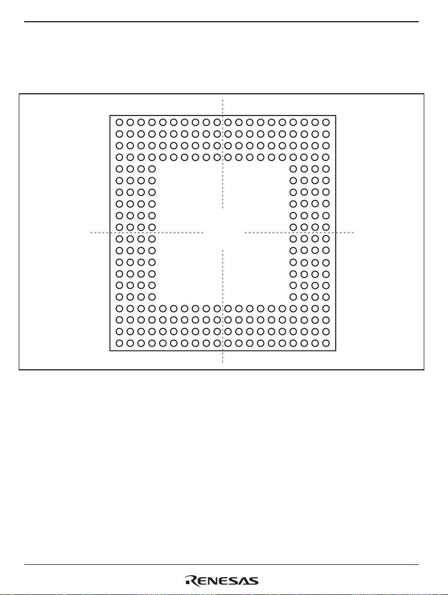
Section 1 Overview
1.3 Pin Assignments
The pin assignments of this LSI is shown in figure 1.2.
2 3 4 5 6 7 8 9 1011121314151617181920
1
A
B
C
D
E
F
G
H
J
K
L
M
N
P
R
T
U
V
W
Y
1 2 3 4 5 6 7 8 9 10111213141516171819
SH7641
BGA-256
(Top view)
A
B
C
D
E
F
G
H
J
K
L
M
N
P
R
T
U
V
W
Y
20
Figure 1.2 Pin Assignments (BGA-256)
Rev. 4.00 Sep. 14, 2005 Page 8 of 828
REJ09B0023-0400
Page 59

Section 1 Overview
1.4 Pin functions
Table 1.2 summarizes the pin functions.
Table 1.2 Pin functions
No.
(BGA256) Pin Name Description
B2 D7 Data bus
C2 D6 Data bus
D2 D5 Data bus
B1 D4 Data bus
E2 D3 Data bus
E3 D2 Data bus
C1 VssQ Ground for I/O circuits (0V)
D3 D1 Data bus
D1 VccQ Power supply for I/O circuits (3.3V)
E4 D0 Data bus
F2 CS3/PTA[3] Chip select 3/Port A
F3 Vss Ground (0V)
E1 CS2/PTA[2] Chip select 2/Port A
F4 Vcc Power supply (1.8V)
G2 UCLK/PTB[0] USB external input clock/Port B
G3 VBUS/PTB[1] USB power detection/Port B
F1 SUSPND/PTB[2] USB suspend/Port B
G4 XVDATA/PTB[3] Receive data input from USB differential receiver/Port B
H2 TXENL/PTB[4] USB output enable/Port B
H3 VccQ Power supply for I/O circuits (3.3V)*
G1 DP D+
H1 DM DH4 VssQ Power supply for US I/O circuits (0V)*
J3 TXDMNS/PTB[5] D- Transmit output for USB transceiver/Port B
J2 TXDPLS/PTB[6] D+ Transmit output for USB transceiver/Port B
J4 DMNS/PTB[7] USB D- input from Receiver/Port B
3
3
Rev. 4.00 Sep. 14, 2005 Page 9 of 982
REJ09B0023-0400
Page 60

Section 1 Overview
No.
(BGA256) Pin Name Description
J1 DPLS/PTB[8] USB D+ input from Receiver/Port B
K3 Vss Ground (0V)
K2 A18 Address bus
K4 Vcc Power supply (1.8V)
K1 A19/PTA[8] Address bus/Port A
L1 A20/PTA[9] Address bus/Port A
L4 A21/PTA[10] Address bus/Port A
M1 A22/PTA[11] Address bus/Port A
L3 A23/PTA[12] Address bus/Port A
L2 A24/PTA[13] Address bus/Port A
M4 VssQ Ground for I/O circuits (0V)
N1 AUDCK AUD clock
M3 VccQ Power supply for I/O circuits (3.3V)
M2 A25/PTA[14] Address bus/Port A
N4 AUDATA[0]/PTJ[8] AUD data/Port J
P1 AUDATA[1]/PTJ[9] AUD data/Port J
N3 AUDATA[2]/PTJ[10] AUD data/Port J
N2 AUDATA[3]/PTJ[11] AUD data/Port J
P4 AUDSYNC/PTJ[12] AUD synchronized/Port J
R1 TCK Test clock
P3 TDI Test data input
T1 TDO Test data output
R4 TMS Test mode select
P2 TRST Test reset
R3 NMI Nonmaskable interrupt request
U1 IRQ0/PTJ[0] External interrupt request/Port J
T4 Vcc Power supply (1.8V)
R2 IRQ1/PTJ[1] External interrupt request/Port J
U4 Vss Ground (0V)
V1 VssQ Ground for I/O circuits (0V)
U2 IRQ2/PTJ[2] External interrupt request/Port J
Rev. 4.00 Sep. 14, 2005 Page 10 of 828
REJ09B0023-0400
Page 61

No.
(BGA256) Pin Name Description
W1 VccQ Power supply for I/O circuits (3.3V)
V3 IRQ3/PTJ[3] External interrupt request/Port J
T2 IRQ4/PTJ[4] External interrupt request/Port J
T3 IRQ5/PTJ[5] External interrupt request/Port J
U3 IRQ6/PTJ[6] External interrupt request/Port J
V2 IRQ7/PTJ[7] External interrupt request/Port J
Y1 SCK0/PTH[0] Serial clock 0/Port H
W2 CTS0/PTH[1] Transmit clear 0/Port H
W3 TxD0/PTH[2] Transmit data 0/Port H
W4 RxD0/PTH[3] Receive data 0/Port H
Y2 RTS0/PTH[4] Transmit request 0/Port H
W5 SCK1/PTH[5] Serial clock 1/Port H
V5 CTS1/PTH[6] Transmit clear 1/Port H
Y3 TxD1/PTH[7] Transmit data 1/Port H
V4 RxD1/PTH[8] Receive data 1/Port H
Y4 RTS1/PTH[9] Transmit request 1/Port H
U5 SCK2/PTH[10] Serial clock 2/Port H
W6 CTS2/PTH[11] Transmit clear 2/Port H
V6 Vss Ground (0V)
Y5 TxD2/PTH[12] Transmit data 2/Port H
U6 Vcc Power supply (1.8V)
W7 RxD2/PTH[13] Receive data 2/Port H
V7 VccQ Power supply for I/O circuits (3.3V)
Y6 RTS2/PTH[14] Transmit request 2/Port H
U7 VssQ Ground for I/O circuits (0V)
W8 TIOC4D/PTE[0] Timer input output 4D/Port E
V8 TIOC4C/PTE[1] Timer input output 4C/Port E
Y7 TIOC4B/PTE[2] Timer input output 4B/Port E
U8 TIOC4A/PTE[3] Timer input output 4A/Port E
Y8 TIOC3D/PTE[4] Timer input output 3D/Port E
V9 TIOC3B/PTE[6] Timer input output 3B/Port E
Section 1 Overview
Rev. 4.00 Sep. 14, 2005 Page 11 of 982
REJ09B0023-0400
Page 62

Section 1 Overview
No.
(BGA256) Pin Name Description
W9 TIOC3C/PTE[5] Timer input output 3C/Port E
U9 TIOC3A/PTE[7] Timer input output 3A/Port E
Y9 TIOC2B/PTE[8] Timer input output 2B/Port E
V10 Vss Ground (0V)
W10 TIOC2A/PTE[9] Timer input output 2A/Port E
U10 Vcc Power supply (1.8V)
Y10 TIOC1B/PTE[10] Timer input output 1B/Port E
Y11 TIOC1A/PTE[11] Timer input output 1A/Port E
U11 TIOC0D/PTE[12] Timer input output 0D/Port E
Y12 TIOC0C/PTE[13] Timer input output 0C/Port E
V11 TIOC0B/PTE[14] Timer input output 0B/Port E
W11 TIOC0A/PTE[15] Timer input output 0A/Port E
U12 VssQ Ground for I/O circuits (0V)
Y13 TCLKD/PTF[8] Timer Clock Input D/Port F
V12 VccQ Power supply for I/O circuits (3.3V)
W12 TCLKC/PTF[9] Timer Clock Input C/Port F
U13 TCLKB/PTF[10] Timer Clock Input B/Port F
Y14 TCLKA/PTF[11] Timer Clock Input A/Port F
V13 POE0/PTF[12] Port output enable input 0/Port F
W13 POE1/PTF[13] Port output enable input 1/Port F
U14 POE2/PTF[14] Port output enable input 2/Port F
Y15 POE3/PTF[15] Port output enable input 3/Port F
V14 PTF[0] Port F
Y16 PTF[1] Port F
U15 PTF[2] Port F
W14 PTF[3] Port F
V15 PTF[4] Port F
Y17 PTF[5] Port F
U16 Vcc Power supply (1.8V)
W15 PTF[6] Port F
U17 Vss Ground (0V)
Rev. 4.00 Sep. 14, 2005 Page 12 of 828
REJ09B0023-0400
Page 63

No.
(BGA256) Pin Name Description
Y18 VssQ Ground for I/O circuits (0V)
W17 PTF[7] Port F
Y19 VccQ Power supply for I/O circuits (3.3V)
V18 PTG[8] Port G
W16 SCL/PTG[9] Serial clock/Port G*
V16 SDA/PTG[10] Serial data/Port G*
2
2
V17 PTG[11] Port G
W18 PTG[12] Port G
Y20 PTG[13] Port G
W19 AVss (AD) Ground for A/D (0V)
V19 AN[0]/PTG[0] A/D converter input/Port G*
U19 AN[1]/PTG[1] A/D converter input/Port G*
W20 AN[2]/PTG[2] A/D converter input/Port G*
T19 AN[3]/PTG[3] A/D converter input/Port G*
T18 AN[4]/PTG[4] A/D converter input/Port G*
V20 AN[5]/PTG[5] A/D converter input/Port G*
U18 AN[6]/PTG[6] A/D converter input/Port G*
2
2
2
2
2
2
2
U20 AVcc (AD) Power supply for A/D (3.3V)
T17 AN[7]/PTG[7] A/D converter input/Port G*
2
R19 VccQ*1 Power supply for I/O circuits (3.3V)*
R18 Vss Ground (0V)
T20 DREQ0/PTC[9] DMA request/Port C
R17 Vcc Power supply (1.8V)
P19 DREQ1/PTC[10] DMA request/Port C
P18 STATUS0/PTC[14] Processor status/Port C
R20 STATUS1/PTC[15] Processor status/Port C
P17 BREQ/PTC[6] Bus request/Port C
N19 BACK/PTC[7] Bus acknowledge/Port C
N18 VccQ*1 Power supply for I/O circuits (3.3V)*
P20 VccQ*1 Power supply for I/O circuits (3.3V)*
N17 ASEBRKAK/PTC[13] ASE brake acknowledge/Port C
Section 1 Overview
1
1
1
Rev. 4.00 Sep. 14, 2005 Page 13 of 982
REJ09B0023-0400
Page 64

Section 1 Overview
No.
(BGA256) Pin Name Description
N20 RESETP Power−on Reset request
M18 VccQ Power supply for I/O circuits (3.3V)
M19 VssQ Ground for I/O circuits (0V)
M17 XTAL Clock oscillator pin
M20 EXTAL External clock/Crystal oscillator pin
L18 Vss Ground (0V)
L19 RESETM Manual Reset request
L17 Vcc Power supply (1.8V)
L20 ASEMD0 ASE mode
K20 Vss(PLL2) Ground for PLL 2 (0V)
K17 Vcc(PLL2) Power supply for PLL 2 (1.8V)
J20 Vcc(PLL1) Power supply for PLL 1 (1.8V)
K18 Vss(PLL1) Ground for PLL 1 (0V)
K19 MD3 Bus width set for area 0
J17 MD2 Clock mode set
H20 VccQ*1 Power supply for I/O circuits (3.3V)*
J18 MD0 Clock mode set
J19 CS6B/PTC[4] Chip select 6B/Port C
H17 VssQ Ground for I/O circuits (0V)
G20 CS6A/PTC[3] Chip select 6A/Port C
H18 VccQ Power supply for I/O circuits (3.3V)
H19 CS5B/PTC[2] Chip select 5B/Port C
G17 CS5A/PTC[1] Chip select 5A/Port C
F20 CS4/PTC[0] Chip select 4/Port C
G18 WAIT Hardware wait request
E20 CS0 Chip select 0
F17 BS Bus cycle start
G19 TEND/PTC[8] DMA transfer end/Port C
F18 FRAME/PTC[5] FRAME output/Port C
D20 RD Read strobe
E17 Vcc Power supply (1.8V)
1
Rev. 4.00 Sep. 14, 2005 Page 14 of 828
REJ09B0023-0400
Page 65

No.
(BGA256) Pin Name Description
F19 DACK0/PTC[11] DMA request acknowledge/Port C
D17 Vss Ground (0V)
C20 VssQ Ground for I/O circuits (0V)
D19 DACK1/PTC[12] DMA request acknowledge/Port C
B20 VccQ Power supply for I/O circuits (3.3V)
C18 D31/PTD[15] Data bus/Port D
E19 D30/PTD[14] Data bus/Port D
E18 D29/PTD[13] Data bus/Port D
D18 D28/PTD[12] Data bus/Port D
C19 D27/PTD[11] Data bus/Port D
A20 D26/PTD[10] Data bus/Port D
B19 D25/PTD[9] Data bus/Port D
B18 D24/PTD[8] Data bus/Port D
B17 D23/PTD[7] Data bus/Port D
A19 D22/PTD[6] Data bus/Port D
B16 D21/PTD[5] Data bus/Port D
C16 D20/PTD[4] Data bus/Port D
A18 VssQ Ground for I/O circuits (0V)
C17 D19/PTD[3] Data bus/Port D
A17 VccQ Power supply for I/O circuits (3.3V)
D16 D18/PTD[2] Data bus/Port D
B15 D17/PTD[1] Data bus/Port D
C15 Vss Ground (0V)
A16 D16/PTD[0] Data bus/Port D
D15 Vcc Power supply (1.8V)
B14 CKIO2 System clock output
C14 VccQ Power supply for I/O circuits (3.3V)
A15 CKIO System clock for I/O circuits
D14 VssQ Ground for I/O circuits (0V)
B13 RD/WR Read/Write
C13 VccQ Power supply for I/O circuits (3.3V)
Section 1 Overview
Rev. 4.00 Sep. 14, 2005 Page 15 of 982
REJ09B0023-0400
Page 66

Section 1 Overview
No.
(BGA256) Pin Name Description
A14 WE0/DQMLL D7 to D0 Select signal/DQM (SDRAM)
D13 VssQ Ground for I/O circuits (0V)
A13 WE1/DQMLU D15 to D8 Select signal/DQM (SDRAM)
C12 CASU/PTA[5] CAS for Upper-32M-byte address/Port A
B12 WE3/DQMUU/AH D31 to D24 Select signal/DQM (SDRAM)/
Address hold (MPX)
D12 RASU/PTA[7] RAS for Upper-32M-byte address/Port A
A12 WE2/DQMUL D23 to D16 Select signal/DQM (SDRAM)
C11 Vss Ground (0V)
B11 CKE/PTA[1] CK enable/Port A
D11 Vcc Power supply (1.8V)
A11 CASL/PTA[4] CAS for Lower-32M-byte address/Port A
A10 RASL/PTA[6] RAS for Lower-32M-byte address/Port A
D10 A17 Address bus
A9 A16 Address bus
C10 A15 Address bus
B10 A14 Address bus
D9 A13 Address bus
A8 A12 Address bus
C9 A11 Address bus
B9 A10 Address bus
D8 VssQ Ground for I/O circuits (0V)
A7 A9 Address bus
C8 VccQ Power supply for I/O circuits (3.3V)
B8 A8 Address bus
D7 A7 Address bus
A6 A6 Address bus
C7 A5 Address bus
A5 A4 Address bus
D6 A3 Address bus
B7 A2 Address bus
Rev. 4.00 Sep. 14, 2005 Page 16 of 828
REJ09B0023-0400
Page 67

Section 1 Overview
No.
(BGA256) Pin Name Description
C6 A1 Address bus
A4 A0/PTA[0] Address bus/Port A
D5 Vcc Power supply (1.8V)
B6 D15 Data bus
D4 Vss Ground (0V)
A3 VssQ Ground for I/O circuits (0V)
B4 D14 Data bus
A2 VccQ Power supply for I/O circuits (3.3V)
C3 D13 Data bus
B5 D12 Data bus
C5 D11 Data bus
C4 D10 Data bus
B3 D9 Data bus
A1 D8 Data bus
Notes: Treatment of unused pins: All the I/O buffers except PTG10, PTG9, and PTG 7 to PTG 0
(IIC2 and analog pins) have weak keepers. Weak-keeper circuits are provided on
input/output pins, and fix the pin inputs to high or low level when the pins are not driven
externally. Unused pins that are provided weak-keeper circuits need not to be fixed their
input levels. Fix unused pins that are not provided weak-keeper circuits to high or low level.
1. These pins are not real power supply for LSI, but each pin should be supplied each
specified voltage for correct action.
2. Weak-keeper circuits are not provided on the I/O buffer pins. Accordingly, pull the pins
up or down when they are not in use. Furthermore, do not apply intermediate voltages
to these pins when you are using them as port input pins.
3. H3 and H4 are a pair of power-supply pins located in the nearest position to the USB
module in this LSI.
Insert a bypass capacitor to the pair of pins to improve the electrical characteristic for
the USB input/output.
Rev. 4.00 Sep. 14, 2005 Page 17 of 982
REJ09B0023-0400
Page 68

Section 1 Overview
Table 1.3 lists the pin functions.
Table 1.3 Pin Functions
Classification Symbol I/O Name Function
Power supply
Clock
Vcc I Power supply Power supply for the internal LSI.
Connect all Vcc pins to the system.
There will be no operation if any pins
are open.
Vss I Ground Ground pin. Connect all Vss pins to
the system power supply (0V). There
will be no operation if any pins are
open.
VccQ I Power supply Power supply for I/O pins. Connect
all VccQ pins to the system power
supply. There will be no operation if
any pins are open.
VssQ I Ground Ground pin. Connect all VssQ pins to
the system power supply (0V). There
will be no operation if any pins are
open.
Vcc (PLL1) I PLL1 power
supply
Power supply for the on-chip PLL1
oscillator
Vss (PLL1) I PLL1 ground Ground pin for the on-chip PLL1
oscillator
Vcc (PLL2) I PLL2 power
supply
Power supply for the on-chip PLL2
oscillator
Vcc (PLL2) I PLL2 ground Ground pin for the on-chip PLL2
oscillator
EXTAL I External clock Connected to a crystal resonator.
An external clock signal may also be
input to the EXTAL pin. For
examples of the connection of crystal
resonator or an external clock signal,
see section 4, Clock Pulse
Generator (CPG).
XTAL O Crystal Connected to a crystal resonator.
For examples of the connection of
crystal resonator or an external clock
signal, see section 4, Clock Pulse
Generator (CPG).
Rev. 4.00 Sep. 14, 2005 Page 18 of 828
REJ09B0023-0400
Page 69

Section 1 Overview
Classification Symbol I/O Name Function
Clock
CKIO O System clock Supplies the system clock to external
devices.
CKIO2 O System clock Supplies the system clock to external
devices.
Operating mode
control
MD3, MD2,
MD0
I Mode set Sets the operating mode. Do not
change values on these pins during
operation.
MD2, MD0 set the clock mode, MD3
set the bus-width mode of area 0.
System control
RESETP I Power-on reset When low, this LSI enters the power-
on reset state.
RESETM I Manual reset When low, this LSI enters the
manual reset state.
STATUS1,
STATUS0
BREQ I Bus-mastership
O Status output Indicate that this LSI is in software
standby, reset, or sleep mode.
Low when an external device
request
requests the release of the bus
mastership.
BACK O Bus-mastership
request
acknowledge
Indicates that the bus mastership
has been released to an external
device. Reception of the BACK
signal informs the device which has
output the BREQ signal that it has
acquired the bus.
Interrupts
NMI I Non-maskable
interrupt
IRQ7 to IRQ0 I Interrupt requests
7 to 0
Non-maskable interrupt request pin.
Fix to high level when not in use.
Maskable interrupt request pin.
Selectable as level input or edge
input. The rising edge, falling edge,
and both edges are selectable as
edges.
Address bus A25 to A0 O Address bus Outputs addresses.
Data bus D31 to D0 I/O Data bus 32-bit bidirectional bus.
Bus control
CS0,
CS2 to CS4,
CS5A, CS5B,
O Chip select 0,
2 to 4, 5A, 5B,
6A, 6B
Chip-select signal for external
memory or devices.
CS6A, CS6B
RD O Read Indicates reading of data from
external devices.
Rev. 4.00 Sep. 14, 2005 Page 19 of 982
REJ09B0023-0400
Page 70

Section 1 Overview
Classification Symbol I/O Name Function
Bus control RD/WR O Read/write Read/write signal
BS O Bus start Bus-cycle start
WE3/DQMUU/
AH
O Byte specification Indicates that bits 31 to 24 of the
data in the external memory or
device are being written.
Selects D31 to D24 when SDRAM is
connected.
Address hold signal for address/data
multiplexed I/O.
WE2/DQMUL O Byte specification Indicates that bits 23 to 16 of the
data in the external memory or
device are being written.
Selects D23 to D16 when SDRAM is
connected.
WE1/DQMLU O Byte specification Indicates that bits 15 to 8 of the data
in the external memory or device are
being written.
Selects D15 to D8 when SDRAM is
connected.
WE0/DQMLL O Byte specification Indicates that bits 7 to 0 of the data
in the external memory or device are
being written.
Selects D7 to D0 when SDRAM is
connected.
RASU, RASL O RAS Connected to the RAS pin when the
SDRAM is connected.
CASU, CASL O CAS Connected to the CAS pin when the
SDRAM is connected.
CKE O CK enable Connected to the CKE pin when the
SDRAM is connected.
FRAME O FRAME signal Connects the FRAME signal for the
burst MPX-IO interface.
WAIT I Wait When active, inserts a wait cycle into
the bus cycles during access to the
external space.
Rev. 4.00 Sep. 14, 2005 Page 20 of 828
REJ09B0023-0400
Page 71

Classification Symbol I/O Name Function
Direct memory
access controller
(DMAC)
DREQ0,
DREQ1
DACK0,
DACK1
I DMA-transfer
request
O DMA-transfer
request receive
Input pin for external requests for
DMA transfer.
Output pin for request receive, in
response to external requests for
DMA transfer.
User debugging
interface
(H-UDI)
TEND0 O DMA-transfer end
output
TCK I Test clock Test-clock input pin.
TMS I Test mode select Inputs the test-mode select signal.
Output pin for DMA transfer end
signal
TDI I Test data input Serial input pin for instructions and
data.
TDO O Test data
output
Serial output pin for instructions and
data.
TRST I Test reset Initialization-signal input pin.
Advanced user
debugger
(AUD)
AUDATA3 to
AUDATA0
AUDCK O AUD clock Sync-clock output pin in AUD-trace
O AUD data Data output pins in AUD-trace mode.
mode.
AUDSYNC O AUD sync
signal
Data start-position acknowledgesignal output pin in AIUD-trace
mode.
E10A interface
ASEBRKAK O Break mode
acknowledge
Indicates that the E10A emulator has
entered its break mode.
For the connection with the E10A,
see the SH7641 E10A Emulator
User's Manual (tentative title).
ASEMD0 I ASE mode Sets the ASE mode.
SCL I/O Serial clock pin Serial clock input/output pin I2C bus interface 2
SDA I/O Serial data pin Serial data input/output pin
Section 1 Overview
Rev. 4.00 Sep. 14, 2005 Page 21 of 982
REJ09B0023-0400
Page 72

Section 1 Overview
Classification Symbol I/O Name Function
Multi function timerpulse unit (MTU)
TCLKA
TCLKB
I Clock input External clock input pins
TCLKC
TCLKD
TIOC0A
TIOC0B
TIOC0C
I/O Input capture/
output compare
match
The TGRA_0 to TGRD_0 input
capture input/output compare
output/PWM output pins.
TIOC0D
TIOC1A
TIOC1B
TIOC2A
TIOC2B
TIOC3A
TIOC3B
TIOC3C
I/O Input capture/
output compare
match
I/O Input capture/
output compare
match
I/O Input capture/
output compare
match
The TGRA_1 to TGRB_1 input
capture input/output compare
output/PWM output pins.
The TGRA_2 to TGRB_2 input
capture input/output compare
output/PWM output pins.
The TGRA_3 to TGRD_3 input
capture input/output compare
output/PWM output pins.
TIOC3D
TIOC4A
TIOC4B
TIOC4C
I/O Input capture/
output compare
The TGRA_4 to TGRB_4 input
capture input/output compare
output/PWM output pins
TIOC4D
Port output enable
(POE)
POE3 to
POE0
I Port output
enable
Request signal input to set the high
current pins to the high impedance
status
Serial
communication
interface with FIFO
(SCIF)
SCK0
SCK1
SCK2
RxD0
I/O Serial clock Clock input/output pins
I Received data Data input pins
RxD1
RxD2
TxD0
O Transmitted data Data output pins
TxD1
TxD2
RTS0
I/O Request to send Request to send
RTS1
RTS2
CTS0
I/O Clear to send Clear to send
CTS1
CTS2
Rev. 4.00 Sep. 14, 2005 Page 22 of 828
REJ09B0023-0400
Page 73

Section 1 Overview
Classification Symbol I/O Name Function
USB function
module
XVDATA I Data input Input pin for receive data from USB
differential receiver
DPLS I D+ input Input pin for D+ signal from USB
receiver
DMNS I D- input Input pin for D- signal from USB
receiver
TXDPLS O D+ output D+ transmit output pin to USB
transceiver
TXDMNS O D- output D- transmit output pin to USB
transceiver
TXENL O Output enable Output enable pin to USB
transceiver
VBUS I USB power
USB cable connection monitor pin
supply monitor
SUSPND O Suspend USB transceiver suspend state
output pin
UCLK I USB clock USB clock input pin (48 MHz input)
DP I/O D+ input/output Input/output pin for D+ signal to/from
transceiver
DM I/O D- input/output Input/output pin for D- signal to/from
transceiver
A/D converter AN7 to AN0 I Analog input pins Analog input pins
AVcc I Analog power
supply for the
Power supply pin for the A/D
converter
A/D converter
AVss I Analog ground
for the A/D
The ground pin for the A/D
converter.
converter
Rev. 4.00 Sep. 14, 2005 Page 23 of 982
REJ09B0023-0400
Page 74

Section 1 Overview
Classification Symbol I/O Name Function
I/O ports
PTA14 to
PTA0
PTB8 to
PTB0
PTC15 to
PTC0
PTD15 to
PTD0
PTE15 to
PTE0
PTF15 to
PTF0
PTG13 to
PTG8
PTG7 to
I/O General purpose
port
I/O General purpose
port
I/O General purpose
port
I/O General purpose
port
I/O General purpose
port
I/O General purpose
port
General purpose
I/O
port
I
15 bits general purpose input/output
pins
9 bits general purpose input/output
pins
16 bits general purpose input/output
pins.
16 bits general purpose input/output
pins
16 bits general purpose input/output
pins
16 bits general purpose input/output
pins
14 bits general purpose input/output
and input pins
PTG0
PTH14 to
PTG0
PTJ12 to
PTG0
I/O General purpose
port
I/O General purpose
port
15 bits general purpose input/output
pins
13 bits general purpose input/output
pins
Rev. 4.00 Sep. 14, 2005 Page 24 of 828
REJ09B0023-0400
Page 75

Section 2 CPU
Section 2 CPU
2.1 Registers
This LSI has the same registers as the SH-3. In addition, this LSI also supports the same DSPrelated registers as in the SH-DSP. The basic software-accessible registers are divided into four
distinct groups:
• General registers
• Control registers
• System registers
• DSP registers
With the exception of some DSP registers, all of these registers are 32-bit width. The general
registers are accessible, with R0 to R7 banked to provide access to a separate set of R0 to R7
registers (i.e. R0 to R7_BANK0, and R0 to R7_BANK1)
register bank (RB) bit in the status register (SR) defines which set of banked registers (R0 to
R7_BANK0 or R0 to R7_BANK1) are accessed as general registers, and which are accessed only
by LDC/STC instructions.
depending on the value of the RB bit. The
The control registers can be accessed by LDC/STC instructions. Control registers are:
• SR: Status register
• SSR: Saved status register
• SPC: Saved program counter
• GBR: Global base register
• VBR: Vector base register
• RS: Repeat start register (DSP mode only)
• RE: Repeat end register (DSP mode only)
• MOD: Modulo register (DSP mode only)
Rev. 4.00 Sep. 14, 2005 Page 25 of 982
REJ09B0023-0400
Page 76

Section 2 CPU
The system registers are accessed by the LDS/STS instructions (the PC is software-accessible, but
is included here because its contents are saved in, and restored from, SPC in exception handling).
The system registers are:
• MACH: Multiply and accumulate high register
• MACL: Multiply and accumulate low register
• PR: Procedure register
• PC: Program counter
This section explains the usage of these registers in different modes.
Figures 2.1 and 2.2 show the register configuration in each processing mode.
The DSP mode is switched by means of the DSP bit in the status register.
Rev. 4.00 Sep. 14, 2005 Page 26 of 982
REJ09B0023-0400
Page 77

Section 2 CPU
31
R0_BANK1*
R1_BANK1*
R2_BANK1*
R3_BANK1*
R4_BANK1*
R5_BANK1*
R6_BANK1*
R7_BANK1*
R8
R9
R10
R11
R12
R13
R14
R15
SR
SSR
GBR
MACH
MACL
PR
VBR
PC
SPC
R0_BANK0*
R1_BANK0*
R2_BANK0*
R3_BANK0*
R4_BANK0*
R5_BANK0*
R6_BANK0*
R7_BANK0*
(a) Register configuration for DSP
mode and non_DSP mode (RB = 1)
031
1
,
2
*
2
2
2
2
2
2
2
1
,
3
*
3
3
3
3
3
3
3
(b) Register configuration for DSP
mode and non_DSP mode (RB = 0)
R0_BANK0*
R1_BANK0*
R2_BANK0*
R3_BANK0*
R4_BANK0*
R5_BANK0*
R6_BANK0*
R7_BANK0*
R8
R9
R10
R11
R12
R13
R14
R15
SR
SSR
GBR
MACH
MACL
PR
VBR
PC
SPC
R0_BANK1*
R1_BANK1*
R2_BANK1*
R3_BANK1*
R4_BANK1*
R5_BANK1*
R6_BANK1*
R7_BANK1*
1
0
,
3
*
3
3
3
3
3
3
3
1
,
2
*
2
2
2
2
2
2
2
Notes: 1. The R0 register is used as an index register in indexed register indirect addressing mode
and indexed GBR indirect addressing mode.
2. Bank register
Accessed as a general register when the RB bit is set to 1 in the SR register.
Accessed only by LDC/STC instructions when the RB bit is cleared to 0.
3. Bank register
Accessed as a general register when the RB bit is cleared to 0 in the SR register.
Accessed only by LDC/STC instructions when the RB bit is set to 1.
Figure 2.1 Register Configuration in Each Processing Mode (1)
Rev. 4.00 Sep. 14, 2005 Page 27 of 982
REJ09B0023-0400
Page 78
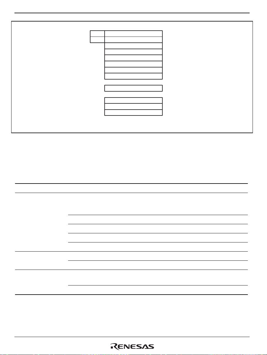
Section 2 CPU
39
32 31
A0G
A1G
(c) DSP mode register configuration (DSP = 1)
A0
A1
M0
M1
X0
X1
Y0
Y1
DSR
MS
ME
MOD
0
Figure 2.2 Register Configuration in Each Processing Mode (2)
Register values after a reset are shown in table 2.1.
Table 2.1 Initial Register Values
Type Registers Initial Value*
General registers R0 to R15 Undefined
Control registers SR RB bit = 1, BL bit = 1, I3 to I0 = 1111 (H'F),
The reserved bits other than bit 30 are all 0;
bit 30 is 1, others undefined
GBR, SSR, SPC Undefined
VBR H'00000000
RS, RE Undefined
MOD Undefined
System registers MACH, MACL, PR Undefined
PC H'A0000000
DSP registers A0, A0G, A1, A1G, M0, M1,
X0, X1, Y0, Y1
DSR H'00000000
Note: * Initialized by a power-on or manual reset.
Undefined
Rev. 4.00 Sep. 14, 2005 Page 28 of 982
REJ09B0023-0400
Page 79
Section 2 CPU
2.1.1 General Registers
There are sixteen 32-bit general registers (Rn), designated R0 to R15. The general registers are
used for data processing and address calculation.
With SuperH microcomputer type instructions, R0 is used as an index register. With a number of
instructions, R0 is the only register that can be used.
With DSP type instructions, eight of the sixteen general registers are used for addressing of X and
Y data memory and data memory (single data) that uses the L-bus.
To access X memory, R4 and R5 are used as the X address register [Ax] and R8 is used as the X
index register [Ix]. To access Y memory, R6 and R7 are used as the Y address register [Ay] and
R9 is used as the Y index register [Iy]. To access single data that uses the L-bus, R2, R3, R4, and
R5 are used as the single data address register [As] and R8 is used as the single data index register
[Is].
Figure 2.3 shows the general registers, which are identical to those of the SH3, when DSP
extension is disabled.
31
2
R0*1,*
2
R1*
2
R2*
2
R3*
2
R4*
2
R5*
2
R6*
2
R7*
R8
R9
R10
R11
R12
R13
R14
R15
0
General Registers (when not in DSP mode)
Notes: 1. R0 functions as an index register in the indexed
register-indirect addressing mode and indexed
GBR-indirect addressing mode. In some
instructions, only R0 can be used as the source
register or destination register.
2. R0 to R7 are banked registers. SR.RB specifies
BANK.
SR.RB = 0; BANK0 is used
SR.RB = 1; BANK1 is used
Figure 2.3 General Registers (Not in DSP Mode)
Rev. 4.00 Sep. 14, 2005 Page 29 of 982
REJ09B0023-0400
Page 80
Section 2 CPU
On the other hand, registers R2 to R9 are also used for DSP data address calculation when DSP
extension is enabled (see figure 2.4). Other symbols that represent the purpose of the registers in
DSP type instructions is shown in [ ].
31
R0
R1
R2 [As]
R3 [As]
R4 [As, Ax]
R5 [As, Ax]
R6 [Ay]
R7 [Ay]
R8 [Ix, Is]
R9 [Iy]
R10
R11
R12
R13
R14
R15
0
General Registers (DSP mode enabled)
X or Y data transfer operation
R4, 5 [Ax]: Address register set for X data memory.
R8 [x]: Index register for address register set Ax.
R6, 7 [Ay]: Address register set for Y data memory.
R9 [Iy]: Index register for address register set Ay.
Single data transfer operation
R2 to 5 [As]: Address register set for memory.
R8 [Is]: Index register for address register set As.
Figure 2.4 General Registers (DSP Mode)
DSP type instructions can access X and Y data memory simultaneously. To specify addresses for
X and Y data memory, two address pointer sets are provided. These are:
R8[Ix], R4,5[Ax] for X memory access, and R9[Iy], R6,7[Ay] for Y memory access.
The symbols R2 to R9 are used by the assembler, but users can use other register names (aliases)
that indicate the purpose of the register in the DSP instruction. The coding in assembler is as
follows.
Ix: .REG (R8)
The name Ix is the alias for R8. Other aliases are as follows.
Ax0: .REG (R4)
Ax1: .REG (R5)
Ix: .REG (R8)
Ay0: .REG (R6)
Rev. 4.00 Sep. 14, 2005 Page 30 of 982
REJ09B0023-0400
Page 81

Section 2 CPU
Ay1: .REG (R7)
Iy: .REG (R9)
As0: .REG (R4) ; This is optional, if another alias is required for single data transfer.
As1: .REG (R5) ; This is optional, if another alias is required for single data transfer.
As2: .REG (R2)
As3: .REG (R3)
Is: .REG (R8) ; This is optional, if another alias is required for single data transfer.
2.1.2 Control Registers
This LSI has 8 control registers: SR, SSR, SPC, GBR, VBR, RS, RE, and MOD (figure 2.5). SSR,
SPC, GBR and VBR are the same as the SH-3 registers. The DSP mode is activated only when
SR.DSP = 1.
Repeat start register RS, repeat end register RE, and repeat counter RC (12-bit part of SR) and
repeat control bits RF0 and RF1 are new registers and control bits which are used for repeat
control. Modulo register MOD and modulo control bits DMX and DMY in SR are also new
register and control bits.
In SR, there are six additional control bits: RC11 to RC0, RF0, RF1, DMX, DMY and DSP. DMX
and DMY are used for modulo addressing control. If DMX is 1, the modulo addressing mode is
effective for the X memory address pointer, Ax (R4 or R5). If DMY is 1, the modulo addressing
mode is effective for the Y memory address pointer, Ay (R6 or R7). However, both X and Y
address pointers cannot be operated in modulo addressing mode even though both DMX and
DMY bits are set. The case where DMX = DMY = 1 is reserved for future expansion. If both
DMX and DMY are set simultaneously, the hardware will provisionally treat only the Y address
pointer as the modulo addressing mode pointer. Modulo addressing is available for X and Y data
transfer operations (MOVX and MOVY), but not for a sing le d a ta transfer operation (MOVS).
RF1 and RF0 hold information on the number of repeat steps, and are set when a SETRC
instruction is executed. When RF1 and RF0 = 00, the current repeat module consists of one
instruction step. RF1 and RF0 = 01 means two instruction steps, RF1 and RF0 = 11 means three
instruction steps, and RF1 and RF0 = 10 means the current repeat module consists of four or more
instructions.
Although RC11 to RC0 and RF1 and RF0 can be changed by a store/load to SR, use of the
dedicated manipulation instruction SETRC is recommended.
SR also has a 12-bit repeat counter, RC, which is used for efficient loop control. The repeat start
register (RS) and repeat end register (RE) are also provided for loop control. They hold the start
Rev. 4.00 Sep. 14, 2005 Page 31 of 982
REJ09B0023-0400
Page 82

Section 2 CPU
and end addresses of a loop (the contents of the RS and RE registers are slightly different from the
actual loop start and end addresses).
The modulo register, MOD, is provided to implement modulo addressing for circular data
buffering. MOD holds the modulo start address (MS) and modulo end address (ME).
In order to access RS, RE and MOD, load/store (control register) instructions for these registers
are provided. An example for RS is as follows:
LDC Rm,RS; Rm -> RS
LDC.L @Rm+,RS; (Rm) -> RS, Rm+4 -> Rm
STC RS,Rn; RS -> Rn
STC.L RS,@-Rn; Rn-4 -> Rn, RS -> (Rn)
Address set instructions for RS and RE are also provided.
LDRS @(disp,PC); disp × 2 + PC -> RS
LDRE @(disp,PC); disp × 2 + PC -> RE
Rev. 4.00 Sep. 14, 2005 Page 32 of 982
REJ09B0023-0400
Page 83

Section 2 CPU
31
0 1 RC 0-0
RB bit: Register bank bit; used to define the general registers.
RB = 1: R0_BANK1 to R7_BANK1 are used as general registers.
R0_BANK0 to R7_BANK0 accessed by LDC/STC instructions.
RB = 0: R0_BANK0 to R7_BANK0 are used as general registers.
R0_BANK1 to R7_BANK1 accessed by LDC/STC instructions.
BL bit: Block bit; used to mask exception.
BL = 1: Interrupts are masked (not accepted)
BL = 0: Interrupts are accepted
RC [11:0]: 12-bit repeat counter
DSP bit: DSP operation mode
DSP = 1: DSP instructions (LDS Rm, DSR/A0/X0/X1/Y0/Y1,
LDS.L @Rm+, DSR/A0/X0/X1/Y0/Y1, STS DSR/A0/X0/X1/Y0/Y1, Rn,
STS.L DSR/A0/X0/X1/Y0/Y1, @–Rn, LDC Rm, RS/RE/MOD,
LDC.L @Rm+, RS/RE/MOD, STC RS/RE/MOD,Rn, STC.L RS/RE/MOD, @–Rn,
LDRS, LDRE, SETRC, MOVS, MOVX, MOVY, Pxxx) are enabled.
DSP = 0: All DSP instructions are treated as illegal instructions; only SH3 instructions are
suppor ted.
DMY bit: Modulo addressing enable for Y side
DMX bit: Modulo addressing enable for X side
Q, M bit: Used by DIV0U/S and DIV1 instructions.
I [3:0]: 4-bit field indicating the interrupt request mask level.
RF [1:0]: Used for repeat control
S bit: Used by the MAC instructions and DSP data.
T bit: The MOVT, CMP/cond, TAS, TST, BT, BF, SETT, CLRT and DT instructions use the T bit to indicate true
Reserved bits: A fixed value (either 0 or 1) is read from each of the bits. When writing, write the values shown in the
28 27 16 15 13 12 11 10 9 8 7 6 5 4 3 2 1 0
DSP
DMY DMX M Q I3 I2 I1 I0
(logic one) or false (logic zero). The ADDV/C, SUBV/C, DIV0U/S, DIV1, NEGC, SHAR/L, SHLR/L,
ROTR/L and ROTCR/L instructions also use the T bit to indicate a carry, borrow, overflow, or underflow.
above register. Operation is not guaranteed if a value other than that given above is written to the
reserved bits.
RF1 RF0
STRB BL
SR (Status register)
Figure 2.5 Control Registers (1)
Rev. 4.00 Sep. 14, 2005 Page 33 of 982
REJ09B0023-0400
Page 84

Section 2 CPU
31 0
SSR
31 0
SPC
31 0
GBR
31 0
VBR
31 0
RS
31 0
RE
31 16 15 0
MOD
ME: Modulo end address, MS: Modulo start address
Saved status register (SSR)
Stores current SR value at time of exception to indicate processor status when returning to instruction stream from
exception handler.
Saved program counter (SPC)
Stores current PC value at time of exception to indicate return address on completion of exception handling.
Global base register (GBR)
Stores base address of GBR-indirect addressing mode. The GBR-indirect addressing mode is used for data transfer
and logical operations on the on-chip peripheral module register area.
Vector base register (VBR)
Stores base address of exception vector area.
Repeat start register (RS)
Used in DSP mode only. Indicates start address of repeat loop.
Repeat end register (RE)
Used in DSP mode only. Indicates address of repeat loop end.
Modulo register (MOD)
Used in DSP mode only.
MD[31:16]: ME: Modulo end address, MD[15:0]: Modulo start address.
In X/Y operand address generation, the CPU compares the address with ME, and if it is the same, loads MS in either
the X or Y operand address register (depending on bits DMX and DMY in the SR register).
ME MS
Saved status register (SSR)
Saved program counter (SPC)
Global base register
Vector base register
Repeat start register
Repeat end register
Modulo register
Figure 2.5 Control Registers (2)
Rev. 4.00 Sep. 14, 2005 Page 34 of 982
REJ09B0023-0400
Page 85
2.1.3 System Registers
This LSI has four system registers, MACL, MACH, PR and PC (figure 2.6).
Section 2 CPU
31
MACH
MACL
31
PR
31
PC
0
Multiply and accumulate high and low registers
(MACH and MACL)
Store the results of multiplicationand accumulation
operations.
0
Procedure register (PR)
Stores the subroutine procedure return address.
Program counter (PC)
0
Indicates the start address of the current instruction.
Figure 2.6 System Registers
The DSR, A0, X0, X1, Y0 and Y1 registers are also treated as system registers. Therefore,
instructions for data transfer between general registers and system registers are supported for these
registers.
2.1.4 DSP Registers
This LSI has eight data registers and one control register as DSP registers (figure 2.7). The data
registers are 32-bit width with the exception of registers A0 and A1. Registers A0 and A1 include
8 guard bits (fields A0G and A1G), giving them a total width of 40 bits.
Three kinds of operation access the DSP data registers. The first is DSP data processing. When a
DSP fixed-point data operation uses A0 or A1 as the source register, it uses the guard bits (bits 39
to 32). When it uses A0 or A1 as the destination register, guard bits 39 to 32 are valid. When a
DSP fixed-point data operation uses a DSP register other than A0 or A1 as the source register, it
sign-extends the source value to bits 39 to 32. When it uses one of these registers as the
destination register, bits 39 to 32 of the result are discarded.
The second kind of operation is an X or Y data transfer operation, "MOVX.W" or "MOVY.W".
This operation accesses the X and Y memories through the 16-bit X and Y data buses (figure 2.8).
The register to be loaded or stored by this operation always comprises the upper 16 bits (bits 31 to
16). X0 or X1 can be the destination of an X memory load and Y0 or Y1 can be the desti nati on o f
a Y memory load, but no other register can be the destination register in this operation.
Rev. 4.00 Sep. 14, 2005 Page 35 of 982
REJ09B0023-0400
Page 86

Section 2 CPU
When data is read into the upper 16 bits of a register (bits 31 to 16), the lower 16 bits of the
register (bits 15 to 0) are automatically cleared. A0 and A1 can be stored in the X or Y memory by
this operation, but no other registers can be stored.
The third kind of operation is a single-data transfer instruction, "MOVS.W" or "MOVS.L". These
instructions access any memory location through the LDB (figure 2.8). All DSP registers connect
to the LDB and can be the source or destination register of the data transfer. These instructions
have word and longword access modes. In word mode, registers to be loaded or stored by this
instruction comprise the upper 16 bits (bits 31 to 16) for DSP registers except A0G and A1G.
When data is loaded into a register other than A0G and A1G in word mode, the lower half of the
register is cleared. When A0 or A1 is used, the data is sign-extended to bits 39 to 32 and the lower
half is cleared. When A0G or A1G is the destination register in word mode, data is loaded into an
8-bit register, but A0 or A1 is not cleared. In longword mode, when the destination register is A0
or A1, it is sign-extended to bits 39 to 32.
Tables 2.2 and 2.3 show the data type of registers used in DSP instructions. Some instructions
cannot use some registers shown in the tables because of instruction code limitations. For
example, PMULS can use A1 as the source register, but cannot use A0. These tables ignore details
of register selectability.
Rev. 4.00 Sep. 14, 2005 Page 36 of 982
REJ09B0023-0400
Page 87
Section 2 CPU
Table 2.2 Destination Register in DSP Instructions
Guard Bits Register Bits
Registers Instructions 39 32 31 16 15 0
A0, A1 DSP Fixed-point, PSHA,
PMULS
Integer, PDMSB Sign-extended 24-bit result Cleared
Logical, PSHL Cleared 16-bit result Cleared
Data
MOVS.W Sign-extended 16-bit data Cleared
transfer
MOVS.L Sign-extended 32-bit data
A0G, A1G MOVS.W Data No update
Data
transfer
MOVS.L Data
DSP Fixed-point, PSHA,
Y0, Y1
M0, M1
Integer, logical,
PMULS
PDMSB, PSHL
MOVX/Y.W, MOVS.W 16-bit result Cleared
Data
transfer
MOVS.L 32-bit data
Sign-extended 40-bit result
No update
32-bit result X0, X1
16-bit result Cleared
Rev. 4.00 Sep. 14, 2005 Page 37 of 982
REJ09B0023-0400
Page 88
Section 2 CPU
Table 2.3 Source Register in DSP Operations
Guard Bits Register Bits
Registers Instructions 39 32 31 16 15 0
A0, A1 DSP Fixed-point, PDMSB,
PSHA
Integer 24-bit data
Logical, PSHL, PMULS 16-bit data
MOVX/Y.W, MOVS.W 16-bit data
A0G, A1G MOVS.W Data
Data
transfer
Data
transfer
MOVS.L 32-bit data
MOVS.L Data
DSP Fixed-point, PDMSB,
Y0, Y1
M0, M1
MOVS.W 16-bit data
Integer Sign* 16-bit data
Data
transfer
PSHA
Logical, PSHL, PMULS 16-bit data
MOVS.L 32-bit data
Note: * The data is sign-extended and input to the ALU.
40-bit data
Sign* 32-bit data X0, X1
Rev. 4.00 Sep. 14, 2005 Page 38 of 982
REJ09B0023-0400
Page 89

Section 2 CPU
313239
A0A0G
A1G
(a) DSP Data Registers
(b) DSP Status Register (DSR)
Reset status
DSR: All zeros
Others: Undefined
A1
M0
M1
X0
X1
Y0
Y1
831
Figure 2.7 DSP Registers
16 bits
16 bits
8 bits 32 bits
MOVS.W,
MOVS.L
A0G
A1G
DSR
MOVX.W
32 039
07
MOVY.W
31 16
0
01234567
DCCS [2:0]VNZGT
LDB
XDB
YDB
MOVS.W,
MOVS.L
A0
A1
M0
M1
X0
X1
Y0
Y1
Figure 2.8 Connections of DSP Registers and Buses
Rev. 4.00 Sep. 14, 2005 Page 39 of 982
REJ09B0023-0400
Page 90

Section 2 CPU
The DSP unit has one control register, the DSP status register (DSR). DSR holds the status of DSP
data operation results (zero, negative, and so on) and has a DC bit which is similar to the T bit in
the CPU. The DC bit indicates one of the status flags. A DSP data processing instruction controls
its execution based on the DC bit. This control affects only the operations in the DSP unit; it
controls the update of DSP registers only. It cannot control operations in the CPU, such as address
register updating and load/store operations. Control bits CS2 to CS0 specify the condition to be
reflected in the DC bit.
Unconditional DSP type data operations, except PMULS, MOVX, MOVY and MOVS, update the
condition flags and DC bit, but no CPU instructions, including MAC instructions, update th e DC
bit. Conditional DSP type instructions do NOT update DSR either.
Rev. 4.00 Sep. 14, 2005 Page 40 of 982
REJ09B0023-0400
Page 91

Section 2 CPU
Table 2.4 DSR Register Bits
Bits Name (Abbreviation) Function
31 to 8 Reserved bits 0: Always read as 0; always use 0 as the write value
7 Signed Greater Than bit (GT) Indicates that the operation result is positive (except 0),
or that operand 1 is greater than operand 2
1: Operation result is positive, or operand 1 is greater
than operand 2
6 Zero bit (Z) Indicates that the operation result is zero (0), or that
operand 1 is equal to operand 2
1: Operation result is zero (0), or operands are equal
5 Negative bit (N) Indicates that the operation result is negative, or that
operand 1 is smaller than operand 2
1: Operation result is negative, or operand 1 is smaller
than operand 2
4 Overflow bit (V) Indicates that the operation result has overflowed
1: Operation result has overflowed
3 to 1 Condition Select bits (CS) Designate the mode for selecting the operation result
status to be set in the DC bit
Do not set these bits to 110 or 111
000: Carry/borrow mode
001: Negative value mode
010: Zero mode
011: Overflow mode
100: Signed greater mode
101: Signed greater than or equal to mode
0 DSP Condition bit (DC) Sets the status of the operation result in the mode
designated by the CS bits
0: Designated mode status has not occurred (false)
1: Designated mode status has occurred
Note: After execution of a PADDC/PSUBC instruction, the DC bit sets the status of the operation
result in carry/borrow mode regardless of the CS bits.
Rev. 4.00 Sep. 14, 2005 Page 41 of 982
REJ09B0023-0400
Page 92
Section 2 CPU
DSR is assigned as a system register and the following load/store instructions are provided:
STS DSR,Rn;
STS.L DSR,@-Rn;
LDS Rn,DSR;
LDS.L @Rn+,DSR;
When DSR is read by an STS instruction, the upper bits (bits 31 to 8) are all 0.
2.2 Data Formats
2.2.1 Register Data Format (Non-DSP Type)
Register operands are always longwo rds (32 bits) (figure 2.9). When the memory operand is only
a byte (8 bits) or a word (16 bits), it is sign-extended into a longword when loaded into a register.
31 0
Longword
Figure 2.9 Longword Operand
2.2.2 DSP-Type Data Formats
This LSI has several different data formats that depend on the instruction. This section explains
the data formats for DSP type instructions.
Figure 2.10 shows three DSP-type data formats with different binary point positions. A CPU-type
data format with the binary point to the right of bit 0 is also shown for reference.
The DSP-type fixed point data format has the bina ry point between bit 31 and bit 30. The DSPtype integer format has the binary point between bit 16 and bit 15. The DSP-type logical format
does not have a binary point. The valid data le ngt h s of t he dat a for mat s d e pen d o n the in struct i o n
and the DSP register.
Rev. 4.00 Sep. 14, 2005 Page 42 of 982
REJ09B0023-0400
Page 93

Section 2 CPU
DSP type fixed point
With guard bits
Without guard bits
Multiplier input
DSP type integer
With guard bits
Without guard bits
Shift amount for
arithmetic shift (PSHA)
Shift amount for
logical shift (PSHL)
DSP type logical
39
31 30 0
S
31 30 0
S
39
31 30 16 15
S
39
32 31 0
S
31 0
S
31 22 0
31 21 0
39 31 16 15 0
16 15
15
16
15
16
S
16
15
S
–28 to +28 – 2
–1 to +1 – 2
0
–1 to +1 – 2
–223 to +2
–215 to +2
–32 to +32
–16 to +16
–31
–31
–15
23
– 1
15
– 1
CPU type integer
Longword
S: Sign bit
: Binary point : Does not affect the operations
31 0
S
–231 to +2
31
– 1
Figure 2.10 Data Formats
The shift amount for the arithmetic shift (PSHA) instruction has a 7-bit field that can represent
values from –64 to +63, but –32 to +32 are valid numbers for the instruction. Also the shift
amount for a logical shift operation has a 6-bit field, but –16 to +16 are valid numbers for the
instruction.
Rev. 4.00 Sep. 14, 2005 Page 43 of 982
REJ09B0023-0400
Page 94

Section 2 CPU
2.2.3 Memory Data Formats
Memory data formats are classified into byte, word, and longword. Byte data can be accessed
from any address, but an address error will occur if word data starting from an address other than
2n or longword data starting from an address other than 4n is accessed. In such cases, the data
accessed cannot be guaranteed (figure 2.11).
Address A + 1 Address A + 3
Address A Address A + 2
31 015
Address A
Address A + 4
Address A + 8
23 7
Byte 0 Byte 1 Byte 2 Byte 3
Word 1Word 0
Longword
Big-endian mode
Figure 2.11 Byte, Word, and Longword Alignment
2.3 Features of CPU Core Instructions
The CPU core instructions are RISC-type instructions with the following features:
Fixed 16-Bit Length: All instructions have a fixed length of 16 bits. This improves program code
efficiency.
One Instruction per State: Pipelining is used, and basic instructions can be executed in one state.
Data Size: The basic data size for operations is longword. Byte, word, or longword can be
selected as the memory access size. Memory byte or word data is sign-extended and operated on
as longword data. Immediate data is sign-extended to longword size for arithmetic operations or
zero-extended to longword size for logical operations.
Rev. 4.00 Sep. 14, 2005 Page 44 of 982
REJ09B0023-0400
Page 95

Section 2 CPU
Table 2.5 Word Data Sign Extension
This LSI's CPU Description Example of Other CPU
MOV.W @(disp,PC),R1
ADD R1,R0
........
.DATA.W H'1234
Note: Immediate data is referenced by @(disp,PC).
Sign-extended to 32 bits, R1
becomes H'00001234, and is then
operated on by the ADD instruction.
ADD.W #H'1234,R0
Load/Store Architecture: Basic operations are executed between registers. In operations
involving memory, data is first loaded into a register (load/store architecture). However, bit
manipulation instructions such as AND are executed directly on memory.
Delayed Branching: Unconditional branch instructions, etc., are executed as delayed branches.
With a delayed branch instruction, the branch is made after execution of the instruction (called the
slot instruction) immediately following the delayed branch instruction. This minimizes disruption
of the pipeline when a branch is made.
With a delayed branch, the actual branch operation occurs after exe cution of the slot instruction.
However, instruction execution for register updating, etc., excluding the branch operation, is
performed in delayed branch instruction → delay slot instruction order. For example, even though
the contents of the register holding the branch destination address are changed in the delay slot,
the branch destination address remains as the register contents prior to the change.
Table 2.6 Delayed Branch Instructions
This LSI's CPU Description Example of Other CPU
BRA TRGET
ADD R1,R0
ADD is executed before branch to
TRGET.
ADD.W R1,R0
BRA TRGET
Multiply/Multiply-and-Accumulate Operations: A 16 × 16 → 32 multiply operat i o n i s
executed in 1 to 2 states, and a 16 × 16 + 64 → 64 multiply-and-accumulate operation in 2 states.
A 32 × 32 → 64 multiply operation and a 32 × 32 + 64 → 64 multiply-and-accumulate operation
are each executed in 2 to 3 states.
T Bit: The result of a comparison is indicated by the T bit in the status register (SR), and a
conditional branch is performed according to whether the result is True or False. Processing speed
has been improved by keeping the number of instructions that modify the T bit to a minimum.
Rev. 4.00 Sep. 14, 2005 Page 45 of 982
REJ09B0023-0400
Page 96

Section 2 CPU
Table 2.7 T Bit
This LSI's CPU Description Example of Other CPU
CMP/GE R1,R0
BT TRGET0
BF TRGET1
ADD #–1,R0
CMP/EQ #0,R0
BT TRGET
If R0 ≥ R1, the T bit is set.
A branch is made to TRGET0
if R0 ≥ R1, or to TRGET1 if R0 < R1.
The T bit is not set by ADD.
If R0 = 0, the T bit is set.
A branch is made if R0 = 0.
CMP.W R1,R0
BGE TRGET0
BLT TRGET1
SUB.W #1,R0
BEQ TRGET
Immediate Data: Byte immediate data is placed inside the instruction code. Word and longword
immediate data is not placed inside the instruction code, but in a table in memory. The table in
memory is referenced with an immediate data transfer instruction (MOV) using PC-relative
addressing mode with displacement.
Table 2.8 Immediate Data Referencing
Type This LSI's CPU Example of Other CPU
8-bit immediate MOV #H'12,R0 MOV.B #H'12,R0
16-bit immediate MOV.W @(disp,PC),R0
........
.DATA.W H'1234
32-bit immediate MOV.L @(disp,PC),R0
........
.DATA.L H'12345678
Note: Immediate data is referenced by @(disp,PC).
MOV.W #H'1234,R0
MOV.L #H'12345678,R0
Absolute Addresses: When data is referenced by an absolute address, the absolute address value
is placed in a table in memory beforehand. Using the method whereby immediate data is loaded
when an instruction is executed, this value is transferred to a register and the data is referenced
using register indirect addressing mode.
Rev. 4.00 Sep. 14, 2005 Page 46 of 982
REJ09B0023-0400
Page 97

Section 2 CPU
Table 2.9 Absolute Address Referencing
Type This LSI's CPU Example of Other CPU
Absolute address MOV.L @(disp,PC),R1
MOV.B @R1,R0
........
.DATA.L H'12345678
MOV.B @H'12345678,R0
16-Bit/32-Bit Displacement: When data is referenced with a 16- or 32-bit displacement, the
displacement value is placed in a table in memory beforehand. Using the method whereby
immediate data is loaded when an instruction is executed, this value is transferred to a register and
the data is referenced using indexed register indirect addressing mode.
Table 2.10 Displacement Referencing
Type This LSI's CPU Example of Other CPU
16-bit displacement MOV.W @(disp,PC),R0
MOV.W @(R0,R1),R2
........
.DATA.W H'1234
MOV.W @(H'1234,R1),R2
Rev. 4.00 Sep. 14, 2005 Page 47 of 982
REJ09B0023-0400
Page 98

Section 2 CPU
2.4 Instruction Formats
2.4.1 CPU Instruction Addressing Modes
The following table shows addressing modes and effective address calculation methods for
instructions executed by the CPU core.
Table 2.11 Addressing Modes and Effective Addresses for CPU Instructions
Addressing
Mode
Instruction
Format
Effective Address Calculation Method Calculation Formula
Register direct Rn Effective address is register Rn.
(Operand is register Rn contents.)
Register indirect @Rn Effective address is register Rn contents.
Rn
Register
indirect with
post-increment
Rn
@Rn+ Effective address is register Rn contents.
A constant is added to Rn after instruction
execution: 1 for a byte operand, 2 for a word
operand, 4 for a longword operand.
Rn
Register
indirect with
pre-decrement
Rn
Rn + 1/2/4
1/2/4
+
@–Rn Effective address is register Rn contents. It is
decremented by a constant beforehand: 1 for
a byte operand, 2 for a word operand, 4 for
a longword operand.
Rn
Rn – 1/2/4
1/2/4
–
Rn – 1/2/4
Rn
Rn
After instruction execution
Byte: Rn + 1 → Rn
Word: Rn + 2 → Rn
Longword: Rn + 4 → Rn
Byte: Rn – 1 → Rn
Word: Rn – 2 → Rn
Longword: Rn – 4 → Rn
(Instruction executed with Rn
after calculation)
Rev. 4.00 Sep. 14, 2005 Page 48 of 982
REJ09B0023-0400
Page 99

Section 2 CPU
Addressing
Mode
Register
indirect with
displacement
Indexed
register indirect
GBR
indirect with
displacement
Indexed GBR
indirect
Instruction
Format
Effective Address Calculation Method Calculation Formula
@(disp:4, Rn) Effective address is register Rn contents with
4-bit displacement disp added. After disp is
zero-extended, it is multiplied by 1 (byte),
2 (word), or 4 (longword), according to the
operand size.
Rn
disp
(zero-extended)
1/2/4
+
×
Rn
+ disp × 1/2/4
@(R0, Rn) Effective address is sum of register Rn and
R0 contents.
Rn
+
R0
Rn + R0
@(disp:8, GBR) Effective address is register GBR contents
with 8-bit displacement disp added.
After disp is zero-extended, it is multiplied by
1 (byte), 2 (word), or 4 (longword), according
to the operand size.
GBR
disp
(zero-extended)
1/2/4
+
×
GBR
+ disp × 1/2/4
@(R0, GBR) Effective address is sum of register GBR and
R0 contents.
GBR
+
R0
GBR + R0
Byte: Rn + disp
Word: Rn + disp × 2
Longword: Rn + disp × 4
Rn + R0
Byte: GBR + disp
Word: GBR + disp × 2
Longword: GBR + disp × 4
GBR + R0
Rev. 4.00 Sep. 14, 2005 Page 49 of 982
REJ09B0023-0400
Page 100

Section 2 CPU
Addressing
Mode
PC-relative with
displacement
Instruction
Format
Effective Address Calculation Method Calculation Formula
@(disp:8, PC) Effective address is PC with 8-bit
displacement disp added. After disp is zeroextended, it is multiplied by 2 (word) or 4
(longword),
according to the operand size. With a
longword operand, the lower 2 bits of PC are
masked.
PC
H'FFFFFFFC
disp
(zero-extended)
2/4
*
&
PC + disp × 2
+
PC&H'FFFFFFFC
×
* : With longword operand
+ disp × 4
or
PC-relative disp:8 Effective address is PC with 8-bit
displacement disp added after being signextended and multiplied by 2.
PC
+
disp
(sign-extended)
2
×
PC + disp × 2
disp:12 Effective address is PC with 12-bit
displacement disp added after being signextended and multiplied by 2
PC
+
disp
(sign-extended)
2
×
PC + disp × 2
Rn Effective address is sum of PC and Rn.
PC
+
Rn
PC + Rn
Word: PC + disp × 2
Longword:
PC&H'FFFFFFFC
+ disp × 4
PC + disp × 2
PC + disp × 2
PC + Rn
Rev. 4.00 Sep. 14, 2005 Page 50 of 982
REJ09B0023-0400
 Loading...