

Page 1
HD151TS207SS
Mother Board Clock Generator
for Intel P4+ Chipset (Springdale)
REJ03D0006-0100Z
Preliminary
Rev.1.00
Apr.25.2003
Description
The HD151TS207SS is Intel CK409T type high-performance, low-skew, low-jitter, PC motherboard clock
generator. It is specifically designed for Intel Pentium®4+ chipset.
Features
• 3 differential pairs of current mode control CPU clocks
• 1 differential pair of Serial Reference Clock (SRC), selectable 100 MHz/200 MHz
• 6 copies PCI clocks and 3 copies PCIF clocks @3.3V, 33.3 MHz
• 1 copy PCI clock @3.3 V, selectable 33.3 MHz/25 MHz
• 1 copy USB clock @3.3 V, selectable 48 MHz/24 MHz
• 1 copy DOT clock @3.3 V, 48 MHz
• 4 copies of 3V66 clocks @3.3 V, 66.6 MHz
• 1 copy of 3V66/VCH clock @3.3 V, selectable 66. 6 MHz/48 MHz
• 2 copies of REF clocks @3.3 V, 14.318 MHz
• Power save and clock stop function
2CTM
• I
• Programmable Clock Control (Spread Spectrum Percentage, Clock Output Skew, Slew Rate)
• Watchdog timer and reset output
• 56pin SSOP (300 mils)
serial port programming
Note: I
Rev.1.00, Apr.25.2003, page 1 of 38
2
C is a trademark of Philips Corporation.
Pentium is registered trademark of Intel Corporation
Page 2

HD151TS207SS
Key Specifications
• Supply Voltages: VDD = 3.3 V±5%
• CPU clock cycle to cycle jitter = |125ps| (SSC Disabled)
• CPU clock group Skew = 100ps
• 3V66 clock group Skew = 250psmax
• PCI clock group Skew = 500psmax
Rev.1.00, Apr.25.2003, page 2 of 38
Page 3
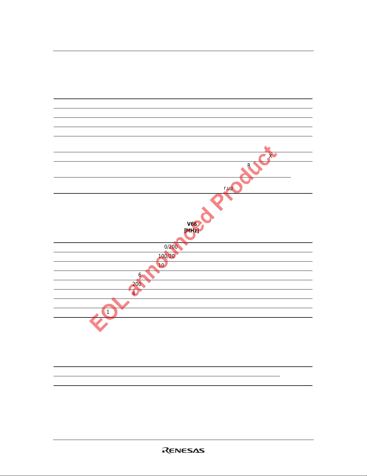
HD151TS207SS
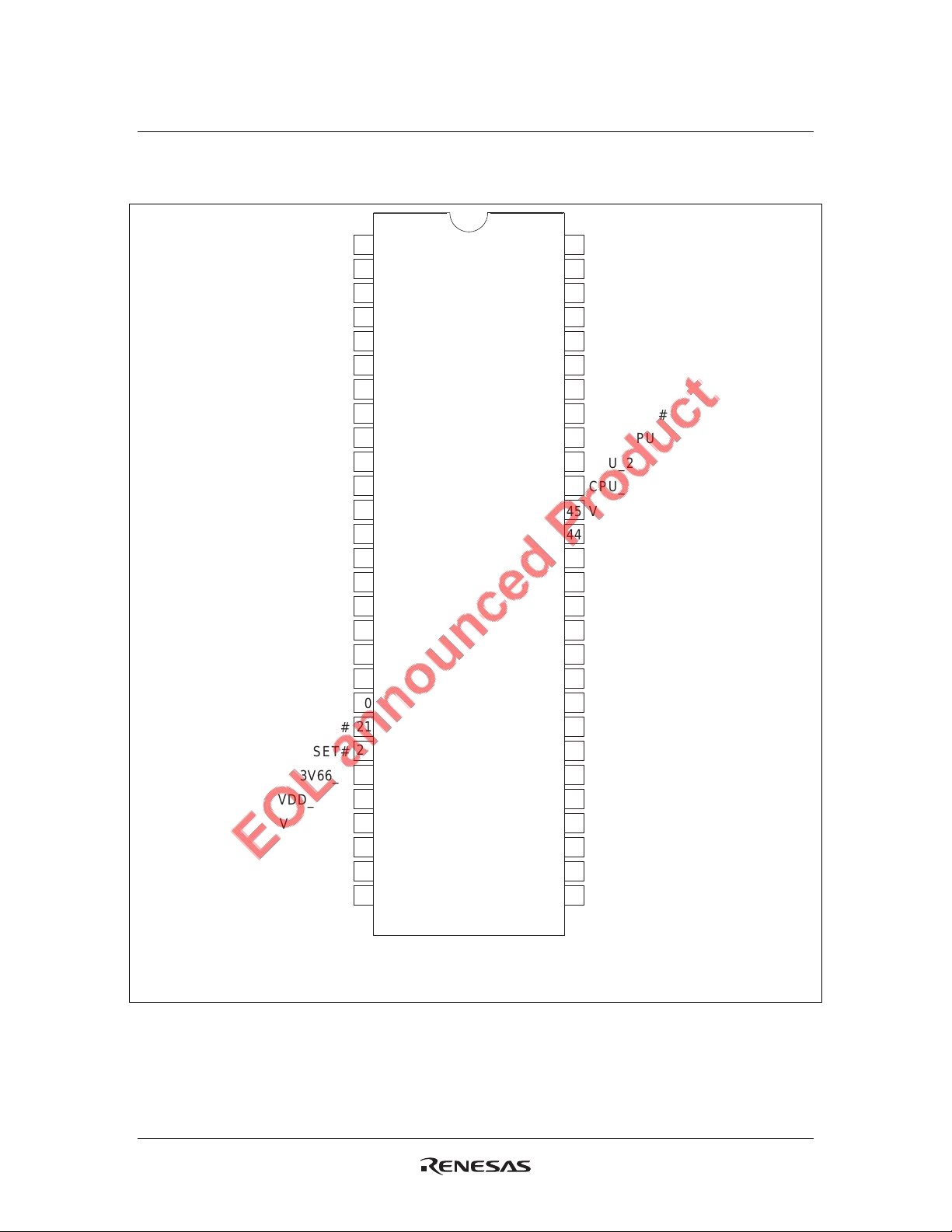
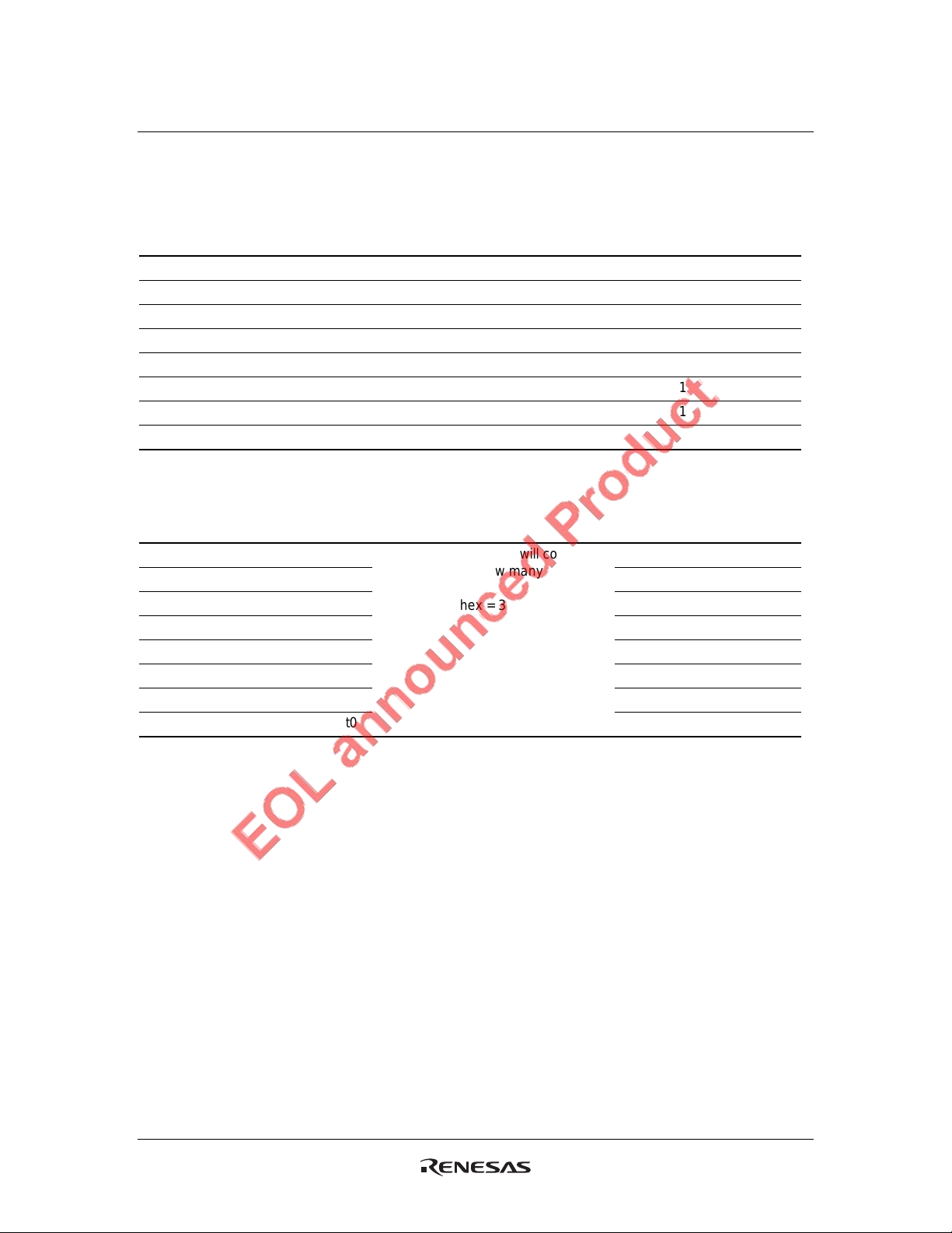
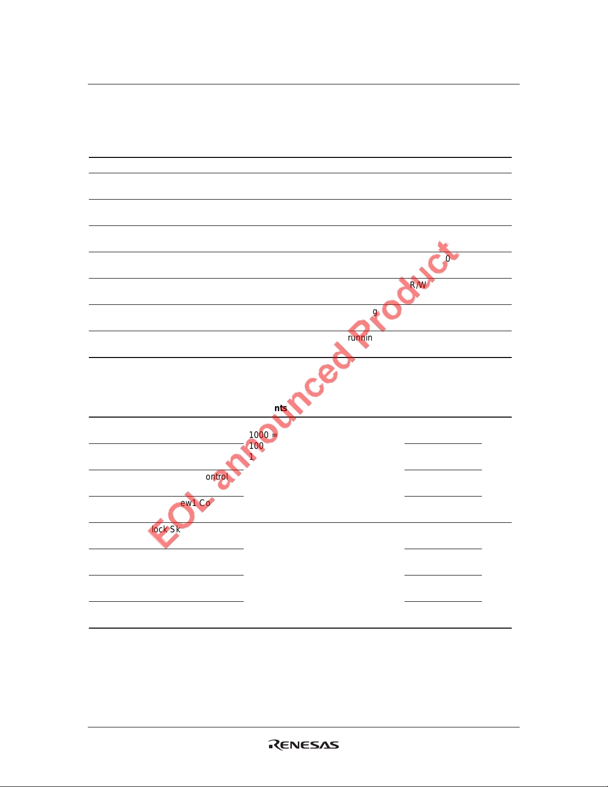
Pin Arrangement
MODE/PCI_0
SEL100_200/PCI_4
SEL33_25/PCI_5
PWRDWN#/SAFE_F#
3V66_0/RESET#
REF0
REF1
VDD_REF
XTAL_IN
XTAL_OUT
VSS_REF
FS2/PCIF_0
FS4/PCIF_1
PCIF_2
VDD_PCI
VSS_PCI
PCI_1
PCI_2
PCI_3
VDD_PCI
VSS_PCI
PCI_6
3V66_1
VDD_3V66
VSS_3V66
3V66_2
3V66_3
SCLK
10
11
12
13
14
15
16
17
18
19
20
21
22
23
24
25
26
27
28
FS_B
1
2
3
4
5
6
7
8
9
56
VDD_A
55
54
VSS_A
53
VSS_IREF
IREF
52
51
FS_A
50
TEST_CLK#
49
PCI_STOP#
VDD_CPU
48
47
CPU_2
46
CPU_2#
45
VSS_CPU
CPU_1
44
43
CPU_1#
42
VDD_CPU
41
CPU_0
40
CPU_0#
39
VSS_SRC
38
SRC
37
SRC#
VDD_SRC
36
35
VTT_PWRGD#
34
VDD_48
33
VSS_48
FS3/DOT_48
32
31
SEL48_24/USB_48
30
SDATA
29
SEL66_48/3V66_4/VCH
(Top view)
PCI_STOP#, PWRDWN# = 150 kΩ Internal Pull-up
Rev.1.00, Apr.25.2003, page 3 of 38
Page 4
HD151TS207SS
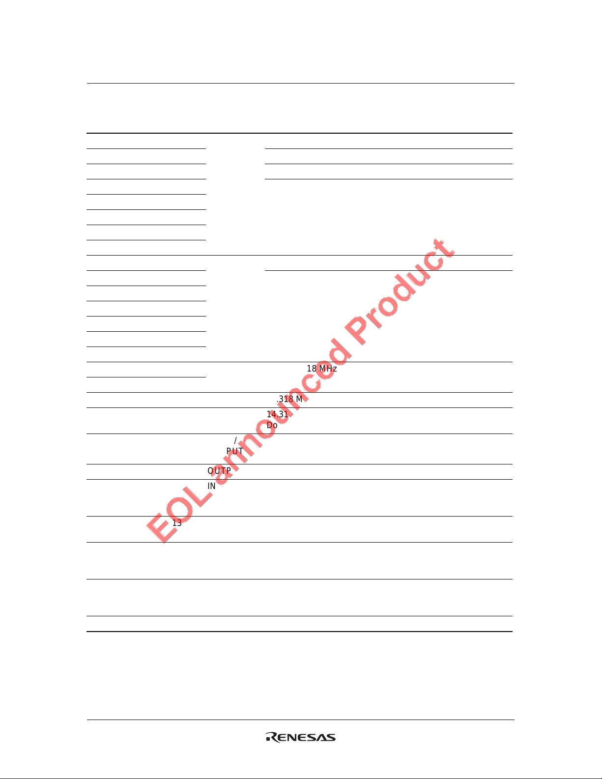
Pin Descriptions
Pin name No. Type Description
VSS_A 54 Ground for PLL
VSS_CPU 45 Ground for outputs
VSS_IREF 53 Ground for current reference
VSS_SRC 39
VSS_3V66 25
VSS_PCI 11, 17
VSS_REF 6
VSS_48 33
VDD_A 55 3.3 V Power Supply for PLL
VDD_CPU 42, 48
VDD_SRC 36
VDD_3V66 24
VDD_PCI 10, 16
VDD_REF 3
VDD_48 34
REF0 1
REF1 2
XTAL_IN 4 INPUT 14.318 MHz XTAL input.
XTAL_OUT 5 OUTPUT 14.318 MHz XTAL output.
FS2/PCIF_[0:1] 7,8 INPUT/
Ground
Ground for outputs
Power
3.3 V Power Supply for outputs
OUTPUT 3.3 V 14.318 MHz reference clock.
Don’t connect when an external clock is applied at XTAL_IN.
Frequency select latch input pin.
OUTPUT
/Free running PCI clock 3.3 V output.
PCIF_2 9 OUTPUT Free running PCI clock 3.3 V output.
**MODE/PCI_0 12 INPUT/
OUTPUT
PCI_[1:3] 13,14,15OUTPUT PCI clock 3.3 V outputs.
**SEL100_200/
PCI_4
**SEL33_25/PCI_5 19 INPUT/
PCI_6 20 OUTPUT PCI clock 3.3 V outputs.
Note: (*): Those pins are 150 kΩ internal pulled-UP.
(**): Those pins are 150 kΩ internal pulled-DOWN.
Rev.1.00, Apr.25.2003, page 4 of 38
18 INPUT/
OUTPUT
OUTPUT
Function select latch input pin for pin 22,
1 = Reset#, 0 = clock output.
/PCI clock 3.3 V output.
Latched select input for SRC output.
1 = 200 MHz, 0 = 100 MHz
/PCI clock 3.3 V output.
Latched select input for PCI5 output.
1 = 25 MHz, 0 = 33 MHz
/PCI clock 3.3 V output.
Page 5

HD151TS207SS
Pin Descriptions (cont.)
Pin name No. Type Description
PWRDWN#/
SAFE_F#
3V66_0/RESET# 22 OUTPUT 3V66 / Watchdog RESET# selectable output.
3V66_[1:3] 23,26,27OUTPUT 3V66 clock 3.3V outputs.
21 INPUT
PULL–UP*
PWRDWN# / SAFE_F# selectable input.
Default is PWRDWN# input.
Byte15[5] = “1” : SAFE_F# input.
PWRDWN# is all clocks stop pin.
Asynchronous active “Low” input.
When asserted low, all output clocks are disabled.
SAFE_F# is active “Low” input.
When SAFE_F# is “Low” ,frequency mode is changed to the
predefined frequency mode.
Default is 3V66 output.
This signal is active low and selected by Mode latch input.
SCLK 28 INPUT
PULL-UP*
**SEL66_48/
3V66_4/VCH
SDATA 30 IN/OUTPUT
**SEL48_24/
USB_48
FS3/DOT_48 32 INPUT/
VTT_PWRGD# 35 INPUT
SRC# 37 OUTPUT “Complementary” clock of Differential Serial Reference Clock.
SRC 38 OUTPUT “True” clock of Differential Serial Reference Clock.
CPU_[0:2]# 40,43,46OUTPUT “Complementary” clock of differential CPU clock.
CPU_[0:2] 41,44,47OUTPUT “True” clock of differential CPU clock.
PCI_STOP# 49 INPUT
TEST_CLK# 50 INPUT
FS_[A:B] 51,52 INPUT CPU clocks frequency select latch input.
IREF 52 INPUT A precision resistor is attached to this pin which is connected
Note: (*): Those pins are 150 kΩ internal pulled-UP.
(**): Those pins are 150 kΩ internal pulled-DOWN
29 INPUT/
OUTPUT
PULL-UP*
31 INPUT/
OUTPUT
OUTPUT
PULL-UP*
PULL–UP*
PULL-UP*
Clock input for I2C logic.
Latched select input for 3V66/VCH output 1 = 48 MHz,
0 = 66.66 MHz. /3V66 or VCH clock output.
Data input for I2C logic.
Latched select input for 48_24 MHz output
1 = 24 MHz, 0 = 48 MHz / 24_48 MHz clock 3.3 V output.
Frequency select latch input pin.
/DOT_48 clock 3.3 V output.
Qualifying input that latches FS_A and FS_B.
When asserted low, FS_A and FS_B are latched.
PCI clocks stop pin. Active “Low” input.
When asserted low, PCI[6:0] and SRC clocks are
synchronously disabled in low state.
Usually this pin does not give to effect PCIF[2:0] clock outputs.
Test clock mode pin. Active “Low” input.
to internal current reference.
A resistor is connected between this pin and GNDIREF.
Rev.1.00, Apr.25.2003, page 5 of 38
Page 6
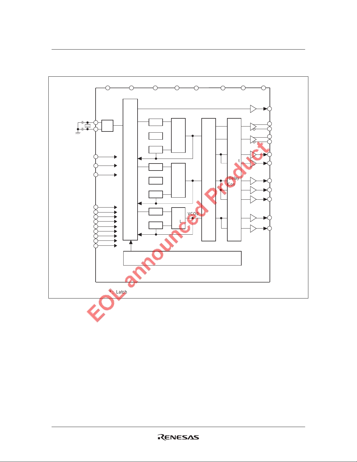
HD151TS207SS
Block Diagram
XTAL
14.318 MHz
PWRDWN#/SAFE_F#
PCI_STOP#
VTT_PWRGD#
TEST_CLK#
*MODE
*SEL100_200
*SEL66_48
*SEL48_24
*SEL33_25
*FS_4/3/2A/B
SCLK
SDATA
3.3 V VDD_48 3.3 V VDD_AVSS_48 VSS_A
CK2
CK1
CK0
1/M2
SSC2
1/N2
1/M1
SSC1
1/N1
1/M0
1/N0
PLL2
For
CPU
PLL1
For
SRC
3V66
PCI
USB
PLL
OSC
Input
Clock
Select
6× 3.3V VDD 6×VSS
VCO2
Clock
VCO1
Divider
VCO0
VSS_IREF IREF
Clock
Select
Delay
Control
Stop
Control
REF[1:0]
(14.318MHz)
CPU[2:0]
CPU[2:0]#
SRC
SRC#
PCI[6:0]
PCIF[2:0]
3V66_0/RESET#
3V66[3:1]
3V66_4/VCH
USB_48
DOT_48
* : Latched Input pin.
Control Logic
Rev.1.00, Apr.25.2003, page 6 of 38
Page 7
HD151TS207SS
I2C Controlled Register Bit Map
Byte0 Control Register
Bit Description Contents Type Default Note
7 Reserved R 0
6 Reserved R 0
5 Reserved R 0
4 Reserved R 0
3 PCI_Stop Reflects the current value
of the external PCI_STOP# pin
2 Reserved R X
1 FS_B Reflects the value of the
FS_B pin sampled on power up
0 FS_A Reflects the value of the
FS_A pin sampled on power up
Table1 Clock Frequency Function Table
0 = PCI_STOP# pin is Low
1 = PCI_STOP# pin is High
0 = FS_B Low at power up
1 = FS_B High at power up
0 = FS_A Low at power up
1 = FS_A High at power up
RX
RX
RX
See
Table
1
Byte6
Bit5
0 0 0 100 100/200 66 33 14.318 48
0 0 1 200 100/200 66 33 14.318 48
0 1 0 133 100/200 66 33 14.318 48
0 1 1 166 100/200 66 33 14.318 48
1 0 0 200 100/200 66 33 14.318 48
1 0 1 400 100/200 66 33 14.318 48
1 1 0 266 100/200 66 33 14.318 48
1 1 1 333 100/200 66 33 14.318 48
FS_A FS_B CPU
[MHz]
SRC
[MHz]
3V66
[MHz]
PCIF
PCI
[MHz]
REF0
REF1
[MHz]
Table2 Test Clock select table
TEST_CLK# CPU
[MHz]
1 REF/2 REF/2 REF/4 REF/8 REF REF/2
0 Hi–Z Hi–Z Hi–Z Hi–Z Hi–Z Hi–Z
Note: 1. REF is a clock over driven on the XIN during test mode.
SRC
[MHz]
3V66
[MHz]
PCIF
PCI
[MHz]
REF0
REF1
[MHz]
USB
DOT
[MHz]
USB
DOT
[MHz]
Note
Note
See Note1,
Table3
Rev.1.00, Apr.25.2003, page 7 of 38
Page 8
HD151TS207SS
I2C Controlled Register Bit Map (cont.)
Table3 FS_A and FS_B pin Input level
Logic Level Min Voltage Max Voltage
0 (Low) 0.35V
1 (High) 0.70V
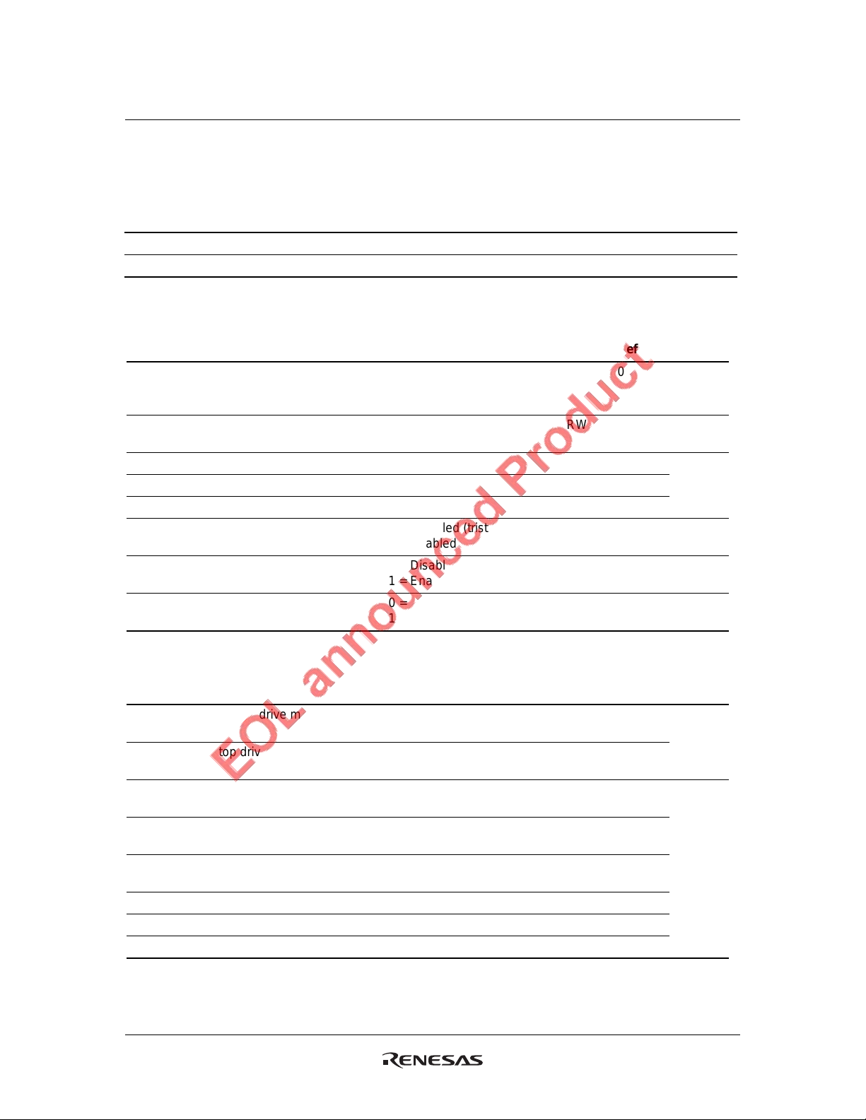
Byte1 Control Register
Bit Description Contents Type Default Note
7 Allow control of SCR with assertion
of PCI_STOP#
6 SRC Output enable 0 = Disabled (tristate)
5 Reserved RW 1
4 Reserved RW 1
3 Reserved RW 1
2 CPU2 Output enable 0 = Disabled (tristate)
1 CPU1 Output enable 0 = Disabled (tristate)
0 CPU0 Output enable 0 = Disabled (tristate)
0 = Free running
1 = Stopped with
PCI_STOP#
1 = Enabled
1 = Enabled
1 = Enabled
1 = Enabled
RW 0 See
Table5
RW 1
RW 1
RW 1
RW 1
Byte2 Control Register
Bit Description Contents Type Default Note
7 SRC_Pwrdwn drive mode 0 = Driven in power down,
1 = Tristate
6 SRC_Stop drive mode 0 = Driven when stopped,
1 = Tristate
5 CPU2_Pwrdwn drive mode 0 = Driven in power down,
1 = Tristate
4 CPU1_Pwrdwn drive mode 0 = Driven in power down,
1 = Tristate
3 CPU0_Pwrdwn drive mode 0 = Driven in power down,
1 = Tristate
2 Reserved RW 0
1 Reserved RW 0
0 Reserved RW 0
Rev.1.00, Apr.25.2003, page 8 of 38
RW 0
RW 0
RW 0
RW 0
RW 0
See
Table5
See
Table4
Page 9
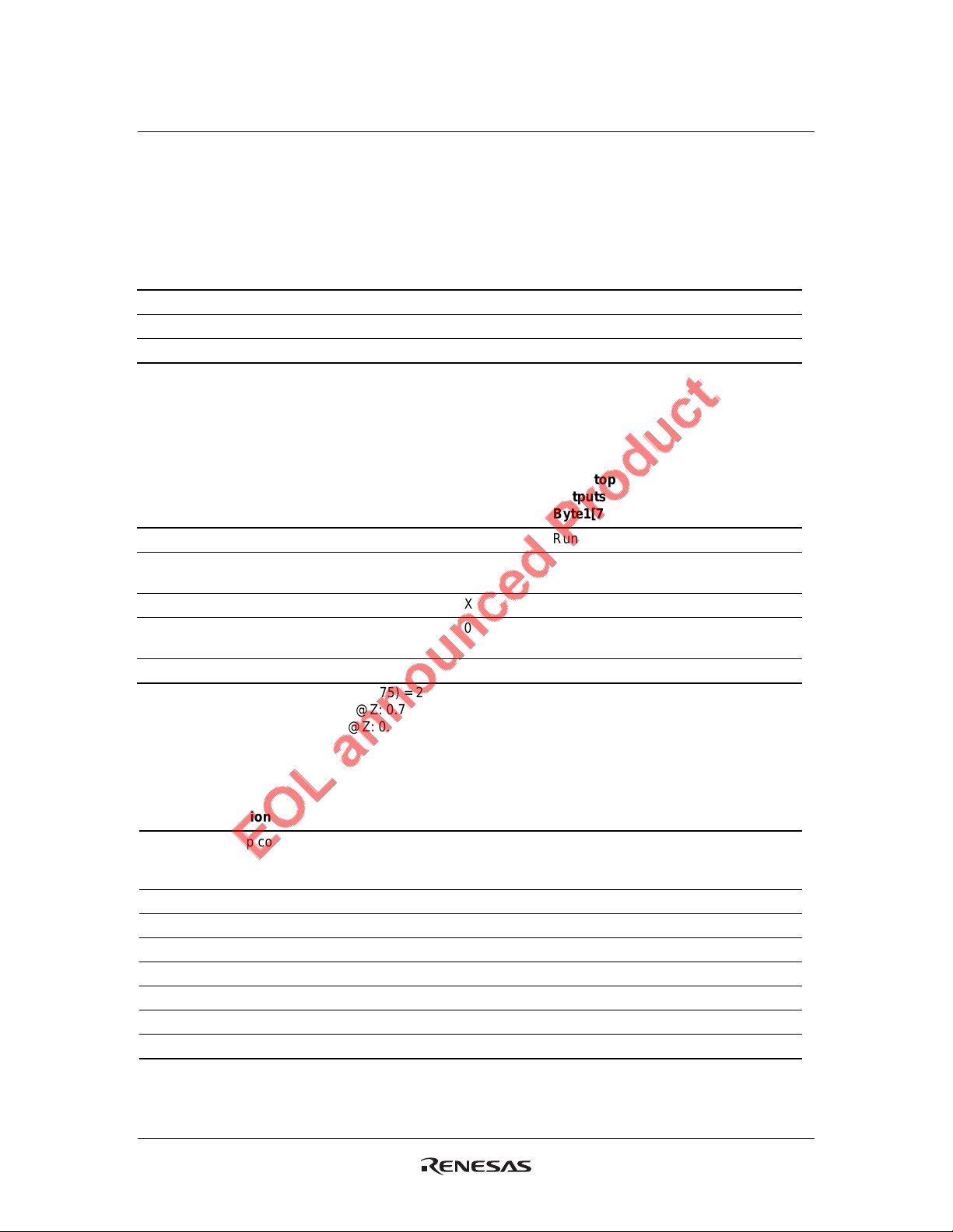
HD151TS207SS
I2C Controlled Register Bit Map (cont.)
Table4 CPU Clock Power Management Truth Table
Signal Pin
PWRDWN#
CPU[2:0] 1 X Running
CPU[2:0] 0 0 Driven @ Iref x2 See Note1
CPU[2:0] 0 1 Tristate
Note: 1. Iref = VDD/(3Rr) = 3.3/(3x475) = 2.32 mA,
Iref x2 = 4.6 mA (Voh @Z: 0.23 V @50 Ω)
PWRDWN#
Tristate Bit
Byte2[5:3]
Non-Stop
Outputs
Byte1[5:3] = 1
Note
Table5 SRC Clock Power Management Truth Table
Signal Pin
PWRDWN#
SRC 1 1 X X Running Running
SRC100XRunningDriven @
SRC101XRunningTristate
SRC 0 X X 0 Driven @
SRC 0 X X 1 Tristate Tristate
Note: 1. Iref = VDD/(3Rr) = 3.3/(3x475) = 2.32 mA
Iref x6 = 13.9 mA (Voh @Z: 0.7 V @50 Ω)
Iref x2 = 4.6 mA (Voh @Z: 0.23 V @50 Ω)
Pin
PCI_STOP#
PCI_STOP#
Tristate Bit
Byte2[6]
PWRDWN#
Tristate Bit
Byte2[7]
Non-Stop
Outputs
Byte1[7] = 1
Iref x2
Stoppable
Outputs
Byte1[7] = 0
Iref x6
Driven @
Iref x2
Note
See Note1
See Note1
Byte3 Control Register
Bit Description Contents Type Default Note
7 PCI_Stop control 0 = Enabled, all stoppable PCI
and SRC clocks are stopped.
1 = Disabled
6 PCI_6 Output enable 0 = Disabled, 1 = Enabled RW 1
5 PCI_5 Output enable 0 = Disabled, 1 = Enabled RW 1
4 PCI_4 Output enable 0 = Disabled, 1 = Enabled RW 1
3 PCI_3 Output enable 0 = Disabled, 1 = Enabled RW 1
2 PCI_2 Output enable 0 = Disabled, 1 = Enabled RW 1
1 PCI_1 Output enable 0 = Disabled, 1 = Enabled RW 1
0 PCI_0 Output enable 0 = Disabled, 1 = Enabled RW 1
Rev.1.00, Apr.25.2003, page 9 of 38
RW 1
Page 10
HD151TS207SS
I2C Controlled Register Bit Map (cont.)
Byte4 Control Register
Bit Description Contents Type Default Note
7 USB_48 2x output drive 0 = 2x Drive strength,
1 = Normal
6 USB_48MHz Output Enable 0 = Disabled,
1 = Enabled
5 Allow control of PCIF_2 with
assertion of PCI_STOP#
4 Allow control of PCIF_1 with
assertion of PCI_STOP#
3 Allow control of PCIF_0 with
assertion of PCI_STOP#
2 PCIF_2 Output enable 0 = Disabled, 1 = Enabled RW 1
1 PCIF_1 Output enable 0 = Disabled, 1 = Enabled RW 1
0 PCIF_0 Output enable 0 = Disabled, 1 = Enabled RW 1
0 = Free Running
1 = Stopped with PCI_STOP#
0 = Free Running
1 = Stopped with PCI_STOP#
0 = Free Running
1 = Stopped with PCI_STOP#
Byte5 Control Register
Bit Description Contents Type Default Note
7 DOT_48MHz Output Enable 0 = Disabled, 1 = Enabled RW 1
6 Reserved RW 1
5 VCH Select 66MHz / 48MHz 0 = 3V66 mode
1 = VCH (48 MHz) mode
4 3V66_4/VCH Output Enable 0 = Disabled (tristate),
1 = Enabled
3 3V66_3 Output Enable 0 = Disabled, 1 = Enabled RW 1
2 3V66_2 Output Enable 0 = Disabled, 1 = Enabled RW 1
1 3V66_1 Output Enable 0 = Disabled, 1 = Enabled RW 1
0 3V66_0 Output Enable 0 = Disabled, 1 = Enabled RW 1
RW 0
RW 1
RW 0
RW 0
RW 0
RW 0
RW 1
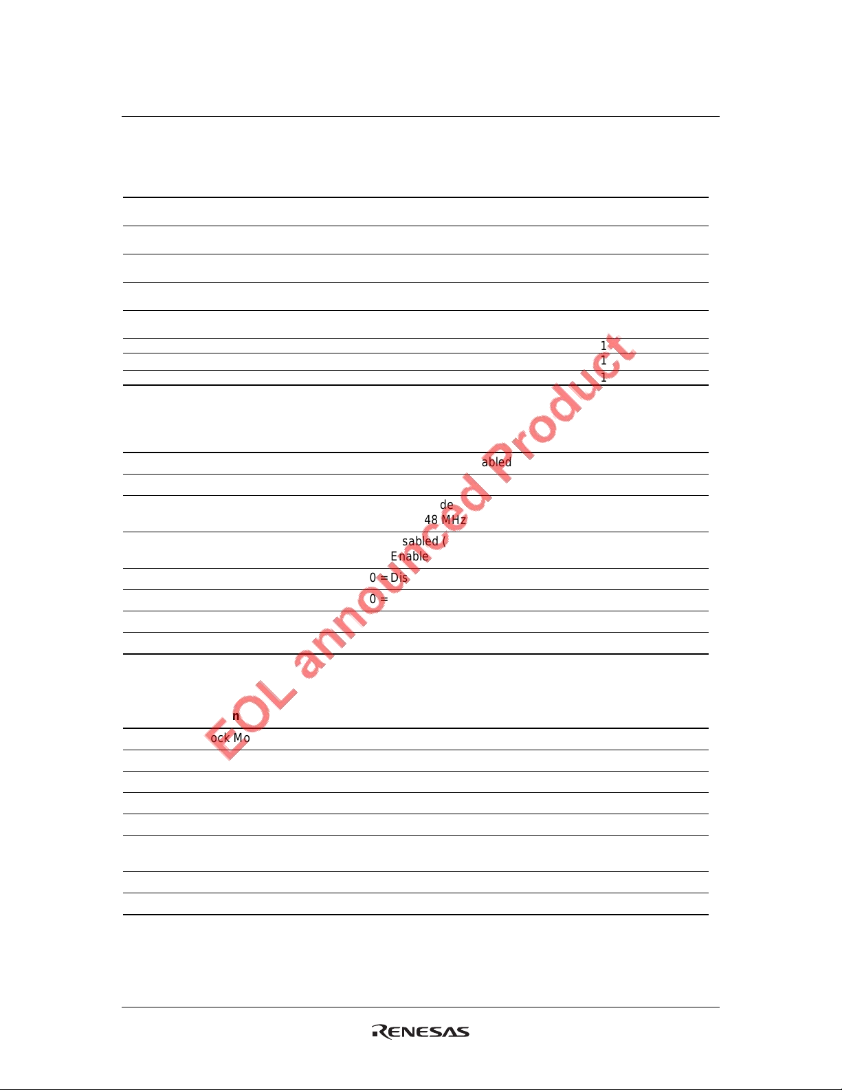
Byte6 Control Register
Bit Description Contents Type Default Note
7 Test Clock Mode 0 = Disabled, 1 = Enabled RW 0
6 Reserved RW 0
5 FS_A & FS_B Operation 0 = Normal, 1 = Test mode RW 0
4 SRC Frequency Sel ect 0 = 100MHz, 1 = 200 MHz RW 0
3 Reserved RW 0
2 Spread Spectrum Mode 0 = Spread OFF
1 = Spread ON
1 REF1 Output Enable 0 = Disabled, 1 = Enabled RW 1
0 REF0 Output Enable 0 = Disabled, 1 = Enabled RW 1
Rev.1.00, Apr.25.2003, page 10 of 38
RW 0 See
B9[7:6]
Page 11
HD151TS207SS
I2C Controlled Register Bit Map (cont.)
Byte7 Vendor Identification Register
Bit Description Contents Type Default Note
7 Revision Code Bit3 Vendor Specific R 0
6 Revision Code Bit2 Vendor Specific R 0
5 Revision Code Bit1 Vendor Specific R 0
4 Revision Code Bit0 Vendor Specific R 1
3 Vendor ID Bit3 Vendor Specific R 1
2 Vendor ID Bit2 Vendor Specific R 1
1 Vendor ID Bit1 Vendor Specific R 1
0 Vendor ID Bit0 Vendor Specific R 1
Byte8 Read Back Byte Count Register
Bit Description Contents Type Default Note
7 Read back byte count Bit7 RW 0
6 Read back byte count Bit6 RW 0
5 Read back byte count Bit5 RW 0
4 Read back byte count Bit4 RW 1
3 Read back byte count Bit3 RW 1
2 Read back byte count Bit2 RW 1
1 Read back byte count Bit1 RW 1
0 Read back byte count Bit0
Writing to this register will configure
byte Count and how many bytes will
be read back.
Default is 1Ehex = 30 bytes.
RW 0
Rev.1.00, Apr.25.2003, page 11 of 38
Page 12

HD151TS207SS
I2C Controlled Register Bit Map (cont.)
Byte9 Control Register
Bit Description Contents Type Default Note
7 SSC2 Enable Bit B6[2] = 0 or B9[7] = 1 : SSC2 =OFF
B6[2] = 1 & B9[7] = 0 : SSC2 = ON
6 SSC1 Enable Bit B6[2] = 0 or B9[6] = 1 : SSC1 = OFF
B6[2] = 1 & B9[6] = 0 : SSC1 = ON
5 Clock Frequency Control
Bit4
4 Clock Frequency Control
Bit3
3 Clock Frequency Control
Bit2
2 Clock Frequency Control
Bit1
1 Clock Frequency Control
Bit0
0 Frequency Select Mode Bit 0 = Fr eq. is selected by latched input
Latched input PCIF_1 at Power ON RW X
Latched input DOT48 at Power ON RW X
Latched input PCIF_0 at Power ON RW X
Latched input FS_A at Power ON RW X
Latched input FS_B at Power ON RW X
FS_A and FS_B
1 = Freq. is selected by I
2
C B9[5:1]
RW 0
RW 0
See
Table
6
RW 0
Rev.1.00, Apr.25.2003, page 12 of 38
Page 13

HD151TS207SS
I2C Controlled Register Bit Map (cont.)
Table6 Clock Frequency Function Table
FS_4 FS_3 FS_2 FS_A FS_BNo.
B9[5] B9[4] B9[3] B9[2] B9[1]
0 0 0 0 0 0 100.02 100.02 66.68 33.34
1 0 0 0 0 1 200.03 100.02 66.68 33.34
2 0 0 0 1 0 133.36 100.02 66.68 33.34
3 0 0 0 1 1 166.69 100.02 66.68 33.34
4 0 0 1 0 0 200.03 100.02 66.68 33.34
5 0 0 1 0 1 400.07 100.02 66.68 33.34
6 0 0 1 1 0 266.71 100.02 66.68 33.34
7 0 0 1 1 1 333.39 100.02 66.68 33.34
8 0 1 0 0 0 138.69 100.02 66.68 33.34
9 0 1 0 0 1 142.25 100.02 66.68 33.34
10 0 1 0 1 0 145.80 100.02 66.68 33.34
11 0 1 0 1 1 149.36 100.02 66.68 33.34
12 0 1 1 0 0 152.91 100.02 66.68 33.34
13 0 1 1 0 1 156.47 100.02 66.68 33.34
14 0 1 1 1 0 160.03 100.02 66.68 33.34
15 0 1 1 1 1 163.58 100.02 66.68 33.34
16 1 0 0 0 0 167.14 100.02 66.68 33.34
17 1 0 0 0 1 170.70 100.02 66.68 33.34
18 1 0 0 1 0 174.25 100.02 66.68 33.34
19 1 0 0 1 1 177.81 100.02 66.68 33.34
20 1 0 1 0 0 181.36 100.02 66.68 33.34
21 1 0 1 0 1 184.92 100.02 66.68 33.34
22 1 0 1 1 0 186.70 100.02 66.68 33.34
23 1 0 1 1 1 189.36 100.02 66.68 33.34
24 1 1 0 0 0 192.03 100.02 66.68 33.34
25 1 1 0 0 1 194.70 100.02 66.68 33.34
26 1 1 0 1 0 197.37 100.02 66.68 33.34
27 1 1 0 1 1 200.03 100.02 66.68 33.34
28 1 1 1 0 0 202.70 100.02 66.68 33.34
29 1 1 1 0 1 205.37 100.02 66.68 33.34
30 1 1 1 1 0 208.03 100.02 66.68 33.34
31 1 1 1 1 1 210.70 100.02 66.68 33.34
CPU
[MHz]
SRC
[MHz]
3V66
[MHz]
PCI
[MHz]
Rev.1.00, Apr.25.2003, page 13 of 38
Page 14

HD151TS207SS
I2C Controlled Register Bit Map (cont.)
Byte10 Control Register
Bit Description Contents Type Default Note
7 RW 0
6 RW 0
5
4 Backup of latch Input FS_4 at
3 Backup of latch Input FS_3 at
2 Backup of latch Input FS_2 at
1 Backup of latch Input FS_A at
0 Backup of latch Input FS_B at
SSC Spread Select Bit[2:0] Bit[2:0] =
000 = –0.500%, 100 = ±0.250%
001 = –0.750%, 101 = ±0.375%
010 = –1.000%, 110 = ±0.500%
011 = –1.500%, 111 = ±0.750%
When SAFE_F# is Enable
Power ON
Power ON
Power ON
Power ON
Power ON
(B15[5]=1)
PWRDWN#/SAFE_F# pin to
“Low”, and if B23[1]=0, frequency
selection is changed to these
setting and
PWRDWN#/SAFE_F# pin to
“High”, frequency selection is
changed back to the last mode.
RW 0
RX
RX
RX
RX
RX
Byte11 Control Register
Bit Description Contents Type Default Note
7 PCI_STOP# Enable Control Bit 0 = Enable , 1 = Disable RW 0
6 CPU_STOP# Enable Control Bit 0 = Enable , 1 = Disable RW 0
5 PWRDWN# Enable Control B it 0 = Enable , 1 = Disable RW 0
4 Backup of B9[5] written by I2CRX
3 Backup of B9[4] written by I2CRX
2 Backup of B9[3] written by I2CRX
1 Backup of B9[2] written by I2CRX
0 Backup of B9[1] written by I2C
When SAFE_F# is Enable
(B15[5]=1)
PWRDWN#/SAFE_F# pin to
“Low”, and if B23[1]=1,
frequency selection is changed to
these setting and
PWRDWN#/SAFE_F# pin to
“High”, frequency selection is
changed back to the last mode.
RX
Rev.1.00, Apr.25.2003, page 14 of 38
Page 15

HD151TS207SS
I2C Controlled Register Bit Map (cont.)
Byte12 Control Register
Bit Description Contents Type Default Note
7 Reserved R/W 0
6 Reserved R/W 0
5 Reserved R/W 0
4 Reserved R/W 0
3 Reserved R/W 0
2 PLL1 Output (VCO1) Frequency
Control Bit
(M1/N1 Divider Control Bit)
PLL1 : for SRC/3V66/PCI_PLL
1 PLL1 N1 Divider Control Bit9 N1[9] R/W 0
0 PLL1 N1 Divider Control Bit8 N1[8] R/W 0
Note: 1. B12[1:0], B13[7:0] and B14[6:0] must be written together (at writing B14) in every case.
0 = Normal mode
PLL1 M1[6:0] and N1[9:0] are
changed on Table 5 selection
decided by FS4/3/2/A/B or
B9[5:1]
1 = Over or Down clocking mode
PLL1 M1[6:0] and N1[9:0] are
changed by B12[1:0], B13[7:0]
and B14[6:0].
B12[1:0], B13[7:0] and B14[6:0]
are able to be changed at B12[2]
= 1.
R/W 0
See.
Note
1
Byte13 Control Register
Bit Description Contents Type Default Note
7 PLL1 N1 Divider Control Bit7 N1[7] R/W 0
6 PLL1 N1 Divider Control Bit6 N1[6] R/W 1
5 PLL1 N1 Divider Control Bit5 N1[5] R/W 0
4 PLL1 N1 Divider Control Bit4 N1[4] R/W 0
3 PLL1 N1 Divider Control Bit3 N1[3] R/W 1
2 PLL1 N1 Divider Control Bit2 N1[2] R/W 0
1 PLL1 N1 Divider Control Bit1 N1[1] R/W 1
0 PLL1 N1 Divider Control Bit0 N1[0] R/W 1
Note: 1. B12[1:0], B13[7:0] and B14[6:0] must be written together (at writing B14) in every case.
Rev.1.00, Apr.25.2003, page 15 of 38
See
Note
1
Page 16
HD151TS207SS
I2C Controlled Register Bit Map (cont.)
Byte14 Control Register
Bit Description Contents Type Default Note
7 Reserved R/W 0
6 PLL1 M1 Divider Control Bit6 M1[6] R/W 0
5 PLL1 M1 Divider Control Bit5 M1[5] R/W 0
4 PLL1 M1 Divider Control Bit4 M1[4] R/W 1
3 PLL1 M1 Divider Control Bit3 M1[3] R/W 0
2 PLL1 M1 Divider Control Bit2 M1[2] R/W 0
1 PLL1 M1 Divider Control Bit1 M1[1] R/W 1
0 PLL1 M1 Divider Control Bit0 M1[0] R/W 0
Note: 1. B12[1:0], B13[7:0] and B14[6:0] must be written together (at writing B14) in every case.
Byte15 Control Register
Bit Description Contents Type Default Note
7 PCI_5 Output Frequency Select
Bit
6 USB_48 Output Frequency
Select Bit
5 SAFE_F# Input mode select Bit 0 = PWRDWN# input mode
4 Clock Divider Control Bit 0 = Normal mode
3 CPU Divider Control Bit3 R/W X
2 CPU Divider Control Bit2 R/W X
1 CPU Divider Control Bit1 R/W X
0 CPU Divider Control Bit0
0 = 33.3 MHz, 1 = 25 MHz R/W 0
0 = 48MHz, 1 = 24 MHz R/W 0
R/W 0
1 = SAFE_F# input mode
Default is PWRDWN# input.
SAFE_F# is active “Low” input.
When SAFE_F# is “Low”,
frequency mode is changed to
the predefined frequency mode.
Predefined frequency mode is
selected by B23[1].
R/W 0
Clock dividers are changed by
Table 5 selection decided B9[5:1]
1 = Over or Down clocking mode
Clock dividers are changed by
B15[3:0] and B16[7:0].
B15[3:0] and B16[7:0] are able to
be changed at B15[4] = 1.
0001 = 1/1,
0010 = 1/2,
0011 = 1/3,
0100 = 1/4,
0101 = 1/5,
0110 = 1/6,
0111 = 1/7
1000 = 1/8
1001 = 1/9
1010 = 1/10
1011 = 1/11
R/W X
See
Note
1
Rev.1.00, Apr.25.2003, page 16 of 38
Page 17
HD151TS207SS
I2C Controlled Register Bit Map (cont.)
Byte16 Control Register
Bit Description Contents Type Default Note
7 3V66 / PCI / PCIF Divider Control
Bit3
6 3V66 / PCI / PCIF Divider Control
Bit2
5 3V66 / PCI / PCIF Divider Control
Bit1
4 3V66 / PCI / PCIF Divider Control
Bit0
3 SRC Divider Control Bit3 R/W X
2 SRC Divider Control Bit2 R/W X
1 SRC Divider Control Bit1 R/W X
0 SRC Divider Control Bit0
3V66 divider ratio =
0010 = 1/2,
0011 = 1/3,
0100 = 1/4,
0101 = 1/5,
0110 = 1/6,
PCI / PCIF divider ratio = 3v66 x
1/2
0001 = 1/1,
0010 = 1/2,
0011 = 1/3,
0100 = 1/4,
0101 = 1/5,
0110 = 1/6
0111 = 1/7
1000 = 1/8
1001 = 1/9
1010 = 1/10
1011 = 1/11
0111 = 1/7
1000 = 1/8
1001 = 1/9
1010 = 1/10
1011 = 1/11
R/W X
R/W X
R/W X
R/W X
R/W X
Byte17 Control Register
Bit Description Contents Type Default Note
7 Reserved R/W 0
6 Reserved R/W 0
5 Reserved R/W 0
4 PLL2 Output (VCO2) Frequency
Control Bit
(M2 / N2 Divider Control Bit)
PLL2 : for CPU
3 VCO2 Frequency Control Bit11 R/W 0
2 VCO2 Frequency Control Bit10 R/W 1
1 VCO2 Frequency Control Bit9 R/W 0
0 VCO2 Frequency Control Bit8
Note: 1. B17[3:0] and B18[7:0] must be written together (at writing B18) in every case.
0 = Normal mode
VCO2 frequency is changed on
Table 5 selection decided by
FS4/3/2/A/B or B9[5:1].
1 = Over or Down clocking mode
VCO2 frequency is changed by
B17[3:0] and B18[7:0] with
decimal.
B17[3:0] and B18[7:0] are able to
be changed at B17[4] = 1.
These bits are 100MHz digit of
VCO2 frequency.
0000 = 0, 0001 = 1 …. 1001 = 9
R/W 0
R/W 0
See
Note
1
Rev.1.00, Apr.25.2003, page 17 of 38
Page 18
HD151TS207SS
I2C Controlled Register Bit Map (cont.)
Byte18 Control Register
Bit Description Contents Type Default Note
7 VCO2 Frequency Control Bit7 R/W 0
6 VCO2 Frequency Control Bit6 R/W 0
5 VCO2 Frequency Control Bit5 R/W 0
4 VCO2 Frequency Control Bit4
3 VCO2 Frequency Control Bit3 R/W 0
2 VCO2 Frequency Control Bit2 R/W 0
1 VCO2 Frequency Control Bit1 R/W 0
0 VCO2 Frequency Control Bit0
Note: 1. B17[3:0] and B18[7:0] must be written together (at writing B18) in every case.
How to set VCO2 frequency to 666 MHz.
These bits are 10MHz digit of
VCO2 frequency.
0000 = 0, 0001 = 1 …. 1001 = 9
These bits are 1MHz digit of
VCO2 frequency.
0000 = 0, 0001 = 1 …. 1001 = 9
See
Note
1
R/W 0
R/W 0
Write
Byte17
00010110
ON
6
Byte18
01100110
How to read actual frequency of VCO2 and CPU clock
Byte17[4] = 1
Actual VCO2 freq. read back.
Byte19
01100110
66
Note: Case of VCO2 = 666.8 MHz.
Other clock frequency are able to read using the same way as shown at upper.
Byte19, Byte20 = Read back of VCO2 actual frequency.
Byte21, Byte22 = Read back of CPU actual frequency.
Byte20
01101000
66
max 720
min 200
86
Rev.1.00, Apr.25.2003, page 18 of 38
Page 19

HD151TS207SS
I2C Controlled Register Bit Map (cont.)
Byte19 Control Register
Bit Description Contents Type Default Note
7 VCO2 Frequency Read Bit1 5 R 0
6 VCO2 Frequency Read Bit1 4 R 0
5 VCO2 Frequency Read Bit1 3 R 0
4 VCO2 Frequency Read Bit12
3 VCO2 Frequency Read Bit1 1 R 0
2 VCO2 Frequency Read Bit1 0 R 0
1 VCO2 Frequency Read Bit9 R 0
0 VCO2 Frequency Read Bit8
Byte20 Control Register
Bit Description Contents Type Default Note
7 VCO2 Frequency Read Bit7 R 0
6 VCO2 Frequency Read Bit6 R 0
5 VCO2 Frequency Read Bit5 R 0
4 VCO2 Frequency Read Bit4
3 VCO2 Frequency Read Bit3 R 0
2 VCO2 Frequency Read Bit2 R 0
1 VCO2 Frequency Read Bit1 R 0
0 VCO2 Frequency Read Bit0
Calculation result of VCO2
frequency.
100 MHz digit
0000 = 0, 0001 = 1 …. 1001 = 9
R0
Calculation result of VCO2
frequency.
10 MHz digit
0000 = 0, 0001 = 1 …. 1001 = 9
R0
Calculation result of VCO2
frequency.
1 MHz digit
0000 = 0, 0001 = 1 …. 1001 = 9
R0
Calculation result of VCO2
frequency.
0.1 MHz digit
0000 = 0, 0001 = 1 …. 1001 = 9
R0
Byte21 Control Register
Bit Description Contents Type Default Note
7 CPU Frequency Read Bit15 R 0
6 CPU Frequency Read Bit14 R 0
5 CPU Frequency Read Bit13 R 0
4 CPU Frequency Read Bit12
3 CPU Frequency Read Bit11 R 0
2 CPU Frequency Read Bit10 R 0
1 CPU Frequency Read Bit9 R 0
0 CPU Frequency Read Bit8
Rev.1.00, Apr.25.2003, page 19 of 38
Calculation result of CPU
frequency.
100 MHz digit
0000 = 0, 0001 = 1 …. 1001 = 9
R0
Calculation result of CPU
frequency.
10 MHz digit
0000 = 0, 0001 = 1 …. 1001 = 9
R0
Page 20

HD151TS207SS
I2C Controlled Register Bit Map (cont.)
Byte22 Control Register
Bit Description Contents Type Default Note
7 CPU Frequency Read Bit7 R 0
6 CPU Frequency Read Bit6 R 0
5 CPU Frequency Read Bit5 R 0
4 CPU Frequency Read Bit4
3 CPU Frequency Read Bit3 R 0
2 CPU Frequency Read Bit2 R 0
1 CPU Frequency Read Bit1 R 0
0 CPU Frequency Read Bit0
Byte23 Control Register
Bit Description Contents Type Default Note
7 Watchdog Enable Control Bit 0 = Disabl e , Pin22 = 3V66_0 output
6 RESET# Reverse Control Bit 0 = Normal , 1 = Reverse R/W 0
5 Watchdog Timer Count Bit3 R/W 1
4 Watchdog Timer Count Bit2 R/W 0
3 Watchdog Timer Count Bit1 R/W 0
2 Watchdog Timer Count Bit0
1 Backup Frequency Select Bit 0 = B10[4:0] , 1 = B11[4:0]
0 Watchdog Status Bit 0 = Normal mode, 1 = Alarm mode R/W 0
Calculation result of CPU frequency.
1 MHz digit
0000 = 0, 0001 = 1 …. 1001 = 9
Calculation result of CPU frequency.
0.1 MHz digit
0000 = 0, 0001 = 1 …. 1001 = 9
1 = Enable , Pin22 = RESET# output
These 4 bits corresponds to how
many watchdog timer will wait from
becoming “Alarm mode” (B23[0] = 1)
to outputting RESET# pin to “Low”.
Default is 586ms x8 = 4.7s at Power
ON
When SAFE_F# is “Low” , frequency
mode is changed to the predefined
frequency mode decided by B10[4:0]
or B11[4:0].
R0
R0
R/W 0
R/W 0
R/W 0
Rev.1.00, Apr.25.2003, page 20 of 38
Page 21
HD151TS207SS
I2C Controlled Register Bit Map (cont.)
Byte24 Control Register
Bit Description Contents Type Default Note
7 Reserved R/W 0
6 PCI_STOP# Stop PCI_6
Control Bit
5 PCI_STOP# Stop PCI_5
Control Bit
4 PCI_STOP# Stop PCI_4
Control Bit
3 PCI_STOP# Stop PCI_3
Control Bit
2 PCI_STOP# Stop PCI_2
Control Bit
1 PCI_STOP# Stop PCI_1
Control Bit
0 PCI_STOP# Stop PCI_0
Control Bit
0 = Stoppable, 1 = Free running R/W 0
0 = Stoppable, 1 = Free running R/W 0
0 = Stoppable, 1 = Free running R/W 0
0 = Stoppable, 1 = Free running R/W 0
0 = Stoppable, 1 = Free running R/W 0
0 = Stoppable, 1 = Free running R/W 0
0 = Stoppable, 1 = Free running R/W 0
Byte25 Control Register
Bit Description Contents Type Default Note
7 CPU Clock Skew1 Control
Bit3
6 CPU Clock Skew1 Control
Bit2
5 CPU Clock Skew1 Control
Bit1
4 CPU Clock Skew1 Control
Bit0
3 CPU Clock Skew2 Control
Bit3
2 CPU Clock Skew2 Control
Bit2
1 CPU Clock Skew2 Control
Bit1
0 CPU Clock Skew2 Control
Bit0
Note: 1. Total CPU Clock Skew is Skew1+Skew2.
Delay Ahead
1000 = +0.00ns, 0111 = –0.20ns
1001 = +0.20ns, 0110 = –0.40ns
1010 = +0.40ns, 0101 = –0.60ns
1011 = +0.60ns, 0100 = –0.80ns
1100 = +0.80ns, 0011 = –1.00ns
1101 = +1.00ns, 0010 = –1.20ns
1110 = +1.20ns, 0001 = –1.40ns
1111 = +1.40ns, 0000 = –1.60ns
Delay Ahead
1000 = +0.00ns, 0111 = –0.15ns
1001 = +0.15ns, 0110 = –0.30ns
1010 = +0.30ns, 0101 = –0.45ns
1011 = +0.45ns, 0100 = –0.60ns
1100 = +0.60ns, 0011 = –0.75ns
1101 = +0.75ns, 0010 = –0.90ns
1110 = +0.90ns, 0001 = –1.05ns
1111 = +1.05ns, 0000 = –1.20ns
R/W 1
R/W 0
R/W 0
R/W 0
R/W 1
R/W 0
R/W 0
R/W 0
See
Note
1
See
Note
1
Rev.1.00, Apr.25.2003, page 21 of 38
Page 22

HD151TS207SS
I2C Controlled Register Bit Map (cont.)
Byte26 Control Register
Bit Description Contents Type Default Note
7 PCIF / PCI Clock Skew2
Control Bit3
6 PCIF / PCI Clock Skew2
Control Bit2
5 PCIF / PCI Clock Skew2
Control Bit1
4 PCIF / PCI Clock Skew2
Control Bit0
3 PCIF / PCI Clock Skew1
Control Bit3
2 PCIF / PCI Clock Skew1
Control Bit2
1 PCIF / PCI Clock Skew1
Control Bit1
0 PCIF / PCI Clock Skew1
Control Bit0
Note: 1. PCIF / PCI Clock Skew is Skew1 (= Normal) or Skew1+Skew2 (= Late).
Skew2 is “Late” Skew that is Delay
Time from “Normal” Skew1.
0000 = +0.0ns, 1000 = +3.2ns
0001 = +0.4ns, 1001 = +3.6ns
0010 = +0.8ns, 1010 = +4.0ns
0011 = +1.2ns, 1011 = +4.4ns
0100 = +1.6ns, 1100 = +4.8ns
0101 = +2.0ns, 1101 = +5.2ns
0110 = +2.4ns, 1110 = +5.6ns
0111 = +2.8ns, 1111 = +6.0ns
Skew1 is “Normal” Skew.
Delay Ahead
1000 = +0.0ns, 0111 = –0.4ns
1001 = +0.4ns, 0110 = –0.8ns
1010 = +0.8ns, 0101 = –1.2ns
1011 = +1.2ns, 0100 = –1.6ns
1100 = +1.6ns, 0011 = –2.0ns
1101 = +2.0ns, 0010 = –2.4ns
1110 = +2.4ns, 0001 = –2.8ns
1111 = +2.8ns, 0000 = –3.2ns
R/W 0
R/W 0
R/W 0
R/W 0
R/W 1
R/W 0
R/W 0
R/W 0
See
Note
1
See
Note
1
Byte27 Control Register
Bit Description Contents Type Default Note
7 Reserved R/W 0
6 PCIF_2 Skew Select Bit 0 = Normal, 1 = Late R/W 0
5 PCIF_1 Skew Select Bit 0 = Normal, 1 = Late R/W 0
4 PCIF_0 Skew Select Bit 0 = Normal, 1 = Late R/W 0
3
2
1
0
Note: 1. Normal = Skew1(B26[3:0]), Late = Skew1(B26[3:0]) +Skew2 (B26[7:4]).
3V66 Clock Skew Control
Bit3
3V66 Clock Skew Control
Bit2
3V66 Clock Skew Control
Bit1
3V66 Clock Skew Control
Bit0
Delay Ahead
1000 = +0.0ns, 0111 = –0.4ns
1001 = +0.4ns, 0110 = –0.8ns
1010 = +0.8ns, 0101 = –1.2ns
1011 = +1.2ns, 0100 = –1.6ns
1100 = +1.6ns, 0011 = –2.0ns
1101 = +2.0ns, 0010 = –2.4ns
1110 = +2.4ns, 0001 = –2.8ns
1111 = +2.8ns, 0000 = –3.2ns
R/W 1
R/W 0
R/W 0
R/W 0
See
Note
1
Rev.1.00, Apr.25.2003, page 22 of 38
Page 23

HD151TS207SS
I2C Controlled Register Bit Map (cont.)
Byte28 Control Register
Bit Description Contents Type Default Note
7 Reserved 0 = Normal, 1 = Late R/W 0
6 PCI_6 Skew Select Bit 0 = Normal, 1 = Late R/W 0
5 PCI_5 Skew Select Bit 0 = Normal, 1 = Late R/W 0
4 PCI_4 Skew Select Bit 0 = Normal, 1 = Late R/W 0
3 PCI_3 Skew Select Bit 0 = Normal, 1 = Late R/W 0
2 PCI_2 Skew Select Bit 0 = Normal, 1 = Late R/W 0
1 PCI_1 Skew Select Bit 0 = Normal, 1 = Late R/W 0
0 PCI_0 Skew Select Bit 0 = Normal, 1 = Late R/W 0
Note: 1. Normal = Skew1(B26[3:0]), Late = Skew1(B26[3:0]) +Skew2 (B26[7:4]).
Byte29 Control Register
Bit Description Contents Type Default Note
7 VCH Slew Rate Control Bit1 R/W 1
6 VCH Slew Rate Control Bit0
5 PCI Slew Rate Control Bit1 R/W 1
4 PCI Slew Rate Control Bit0
3 PCIF Slew Rate Control Bit1 R/W 1
2 PCIF Slew Rate Control Bit0
1 3V66 Slew Rate Control Bit1 R/W 1
0 3V66 Slew Rate Control Bit0
00 = Normal, 10 = “++”
01 = “+“ , 11 = “–”
00 = Normal, 10 = “++”
01 = “+“ , 11 = “–”
00 = Normal, 10 = “++”
01 = “+“ , 11 = “–”
00 = Normal, 10 = “++”
01 = “+“ , 11 = “–”
R/W 0
R/W 0
R/W 0
R/W 0
See
Note
1
Rev.1.00, Apr.25.2003, page 23 of 38
Page 24

HD151TS207SS
6
)
Clock Stop Timing Diagram
PCI_STOP# Assertion/De-assersion
PCI_STOP#
PCI_F
PCI
SRC (Stoppable)
SRC (Stoppable)
SRC# (Stoppable)
PCI_STOP# Assertion/De-assertion Waveforms
PWRDWN# Assertion/De-assersion
PWRDWN#
CPU (Stoppable)
2× Iref (Controled by Byte2[5:3])
Low
Iref (Controled by Byte2[6]
Tristate (Controled by Byte2[6])
Tristate
< 1.8 ms
6× Iref
CPU (Stoppable)
CPU# (Stoppable)
PWRDWN# Assertion/De-assertion Waveforms
PWRDWN# Functionality
PWRDWN#
1 Normal
0
Iref:2
or Float
Float (Controled by Byte2[5:3])
Float
CPU#CPU SRC SRC# 3V66
Normal Normal Normal
Iref:2
Float Float Low
or Float
66MHz
PCIF/PCI
33MHz
Low
6× Iref
USB/DOT
48MHz
Low
REF
14.318MHz
Low
Rev.1.00, Apr.25.2003, page 24 of 38
Page 25

HD151TS207SS
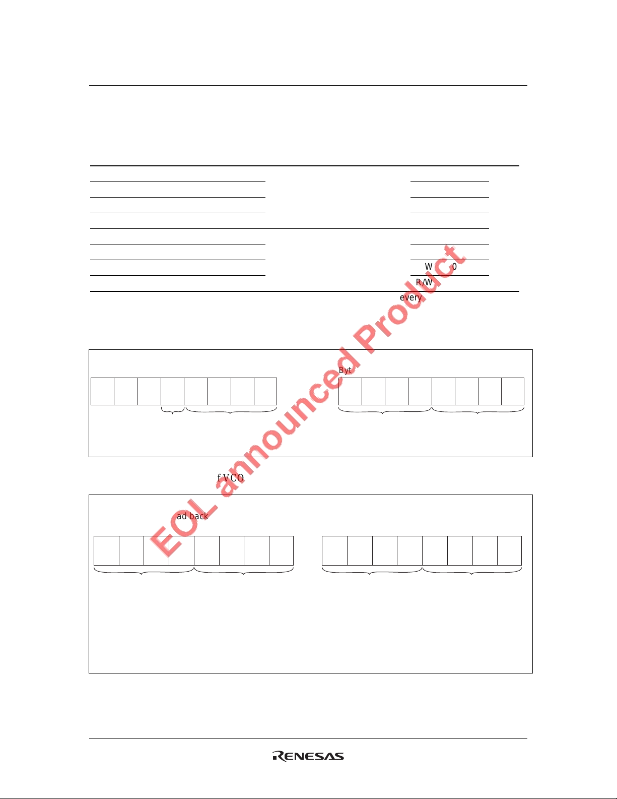
Renesas clock generator I2C Serial Interface Operation
1. Write mode
1.1 Controller (host) sends a start bit.
1.2 Controller (host) sends the write address D2 (h).
1.3 Renesas clock generator will acknowledge (Renesas clock gen. sends “Low”).
1.4 Controller (host) sends a begin byte M.
1.5 Renesas clock generator will acknowledge (Renesas clock gen. sends “Low”).
1.6 Controller (host) sends a byte count N.
1.7 Renesas clock generator will acknowledge (Renesas clock gen. sends “Low”).
1.8 Controller (host) sends data from byte M to byte M+N–1.
1.9 Renesas clock g enerator will ack nowledge each byte one at a time.
1.10 Controller (host) sends a stop bit.
1 bit 1 bit 1 bit 1 bit 1 bit7 bits 8 bits 8 bits 8 bits
Start bit
1 bit
Ack
Slave
address
8 bits 1 bit 1 bit
Byte M+1
1 bit
Ack
R/W
D2(h)
Ack
Begin Byte = M
Ack Ack
Byte Count = N
8 bits
Byte M+N–1
Ack
Byte M
Stop bit
Rev.1.00, Apr.25.2003, page 25 of 38
Page 26

HD151TS207SS
Renesas clock generator I2C Serial Interface Operation (cont.)
2. Read mode
2.1 Controller (host) sends a start bit.
2.2 Controller (host) sends the write address D2 (h).
2.3 Renesas clock generator will acknowledge (Renesas clock gen. sends “Low”).
2.4 Controller (host) sends a begin byte M.
2.5 Renesas clock generator will acknowledge (Renesas clock gen. sends “Low”).
2.6 Controller (host) sends a restart bit.
2.7 Controller (host) sends the read address D3 (h).
2.8 Renesas clock generator will acknowledge (Renesas clock gen. sends “Low”).
2.9 Renesas clock g enerator will sen d the byte count N.
2.10 Controller (host) will acknowledge.
2.11 Renesas clock generator will send data from byte M to byte M+N–1.
2.12 When Renesas clock generator sends the last byte, controller (host) will not acknowledge.
2.13 Controller (host) sends a stop bit.
1 bit 1 bit 1 bit 1 bit 1 bit7 bits 8 bits 7 bits1 bit
Start bit
1 bit
Ack
Begin Count = N
Slave
address
8 bits 1 bit 1 bit
R/W
Ack
D2(h)
1 bit
8 bits 8 bits
Ack
Byte M Byte M+1 Not Ack
Begin Byte = M
1 bit
Ack
1 bit
Ack
Ack
Restart bit
Slave
address
Byte M+N–1
D3(h)
8 bits
R/W
Stop bit
Notes: 1. Renesas clock generator is a slave/receiver, I2C component. It can read back the data stored in
the latches for the verification.
2. The data transfer rate supported by this clock generator is 100k bits/sec or less (standard
mode).
3. The input is operating at 3.3 V logic levels.
4. The data byte format is 8 bit bytes.
5. To simplify the clock generator I
2
C interface, the protocol is set to use only block-write from
the controller.
6. The bytes must be accessed in sequential order from lowest to highest byte with the ability to
stop after any complete byte has been transferred. The data is loaded until a stop sequence is
issued.
7. At power-on, all registers are set to a default condition, as shown.
Rev.1.00, Apr.25.2003, page 26 of 38
Page 27
HD151TS207SS
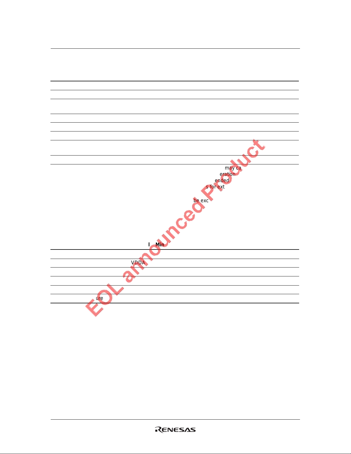
Absolute Maximum Ratings
Item Symbol Ratings Unit Conditions
Supply voltage VDD –0.5 to 4.6 V
Input voltage V
Output voltage *1 V
Input clamp current I
Output clamp current I
Continuous output current I
I
O
IK
OK
O
Maximum power dissipation
at Ta = 55°C (in still air)
Storage temperature Tstg –65 to +150 °C
Notes: Stresses beyond those listed under “absolute maximum ratings” may cause permanent damage
to the device. These are stress ratings only, and functional operation of the device at these or
any other conditions beyond those indicated under “recommended operating conditions” is not
implied. Exposure to absolute maximum rated conditions for extended periods may affect device
reliability.
1. The input and output negative voltage ratings may be exceeded if the input and output clamp
current ratings are observed.
–0.5 to 4.6 V
–0.5 to VDD
+0.5
V
–50 mA VI < 0
–50 mA VO < 0
±50 mA VO = 0 to VDD
0.7 W
Recommended Operating Conditions
Item Symbol Min Typ Max Unit Conditions
Supply voltage VDD 3.135 3.3 3.465 V
Supply voltage VDDA 3.135 3.3 3.465 V
DC input signal voltage –0.3 — VDD+0.3 V
High level input voltage V
Low level input voltage V
Operating temperature T
IH
IL
a
2.0 — VDD+0.3 V
–0.3 — 0.8 V
0—70°C
Rev.1.00, Apr.25.2003, page 27 of 38
Page 28

HD151TS207SS
DC Electrical Characteristics / Serial Input Port
Ta = 0°C to 70°C, VDD = 3.3 V
Item Symbol Min Typ *1Max Unit Test Conditions
Input Low Voltage V
Input High Voltage V
Input Current I
Input capacitance C
IL
IH
I
I
Note: 1. For conditions shown as Min or Max, use the appropriate value specified under recommended
operating conditions.
0.8 V
2.0 V
–50 +50 µA VI = 0 V or 3.465 V,
VDD = 3.465 V
10 pF SDATA & SCLK
AC Electrical Characteristics / Serial Input port
Ta = 0°C to 70°C, VDD = 3.3 V
Item Symbol Min Typ Max Unit Test Conditions Notes
SCLK Frequency F
Start Hold Time t
SCLK Low Time t
SCLK High Time t
Data Setup Time t
Data Hold Time t
Stop Setup Time t
BUS Free Time between
Stop & Start Condition
SCLK
STHD
LOW
HIGH
DSU
DHD
STSU
t
SPF
100 kHz Normal Mode
4.0 µs
4.7 µs
4.0 µs
250 ns
300 ns
4.0 µs
4.7 µs
Rev.1.00, Apr.25.2003, page 28 of 38
Page 29

HD151TS207SS
DC Electrical Characteristics CPU/CPU# Clock
Ta = 0°C to 70°C, VDD = 3.3 V, Iref = 475 Ω
Item Symbol Min Typ *1Max Unit T est Conditions
Output voltage V
Output Current I
O
O
Output resistance 3000 ΩVO = 1.2 V
Notes: 1. For conditions shown as Min or Max, use the appropriate value specified under recommended
operating conditionaI (nom) is output current(Ioh) shown in below.
2. Ioh = VDD/(3Rr) = 3.3/(3x475) = 2.32 mA,
Ioh x6 = 13.89 mA (Voh @Z: 0.695 V @50 Ω),
Ioh x2 = 4.63 mA (Voh @Z: 0.232 V @50 Ω)
1.20 V Rp = 49.9 Ω, VDD = 3.3 V
I(nom) *2 mA VDD = 3.3 V
AC Electrical Characteristics CPU/CPU# Clock (CPU at 0.7V Timing)
Ta = 0°C to 70°C, VDD = 3.3 V, CL = 2 pF, Rs = 33.2 Ω, Rp = 49.9 Ω
Item Symbol Min Typ Max Unit Test Conditions Notes
Cycle to cycle jitter t
CPU Group Skew
(CPU clock out to
CPU clock out)
Rise time t
Fall time t
CCS
t
skS
r
f
|125| ps Note1
|100| ps
175 700 ps VO = 0.175 V
200MHz
to 0.525 V
175 700 ps VO = 0.175 V
200MHz
to 0.525 V
Clock Duty Cycle 45 50 55 % 200MHz
CPU clock period(100) 9.99 ns
CPU clock period(133) 7.49 ns
CPU clock period(166) 5.99 ns
CPU clock period(200) 4.99 ns
Cross point(0.7V) voltage Vcross 0.25 0.55 V 200MHz
Note: 1. Difference of cycle time between two adjoining cycles.
Rev.1.00, Apr.25.2003, page 29 of 38
Page 30

HD151TS207SS
DC Electrical Characteristics SRC/SRC# Clock
Ta = 0°C to 70°C, VDD = 3.3 V, Iref = 475 Ω
Item Symbol Min Typ *1 Max Unit Test Conditions
Output voltage V
Output Current I
O
O
Output resistance 3000 ΩVO = 1.2 V
Notes: 1. For conditions shown as Min or Max, use the appropriate value specified under recommended
operating conditions
2. I(nom) is output current(Ioh) shown in below.
Ioh = VDD/(3Rr) = 3.3/(3x475) = 2.32 mA,
Ioh x6 = 13.89 mA (Voh @Z: 0.695V @50 Ω),
Ioh x2 = 4.63 mA (Voh @Z: 0.232V @50 Ω)
1.20 V Rp = 49.9 Ω, VDD = 3.3 V
I(nom) mA VDD = 3.3 V
AC Electrical Characteristics SRC/SRC# Clock (SRC at 0.7V Timing)
Ta = 0°C to 70°C, VDD = 3.3 V, CL = 2 pF, Rs = 33.2 Ω, Rp = 49.9 Ω
Item Symbol Min Typ Max Unit Test Conditions Notes
Cycle to cycle jitter t
Rise time t
Fall time t
CCS
r
f
Clock Duty Cycle 45 50 55 % 100 MHz
SRC clock period(100) 9.99 ns
SRC clock period(200) 4.99 ns
Cross point(0.7V) voltage Vcross 0.25 0.55 V 100 MHz
Note: 1. Difference of cycle time between two adjoining cycles.
|125| ps Note1
175 700 ps VO = 0.175 V
100 MHz
to 0.525 V
175 700 ps VO = 0.175 V
100 MHz
to 0.525 V
Rev.1.00, Apr.25.2003, page 30 of 38
Page 31

HD151TS207SS
DC Electrical Characteristics / 3V66 Buffer (CK409T Type5 Buffer)
Ta = 0°C to 70°C, VDD = 3.3 V
Item Symbol Min Typ *1 Max Unit Test Conditions
V
OH
V
OL
I
OH
I
OL
Note: 1. For conditions shown as Min or Max, use the appropriate value specified under recommended
operating conditions.
3.1 VI
OH
= –1 mA, VDD = 3.3 VOutput Voltage
50 mV IOL = 1 mA, VDD = 3.3 V
–33 mA VOH = 1.0 VOutput Current
30 mA VOL = 1.95 V
AC Electrical Characteristics / 3V66 Buffer
Ta = 0°C to 70°C, VDD = 3.3 V, CL = 30 pF
Item Symbol Min Typ Max Unit Test Conditions Notes
Cycle to cycle jitter t
3V66 Buffer (3V66 (4:0))
t
CCS
skS
Group Skew
Slew rate t
SL
Clock Period 14.998 ns
Clock Duty Cycle 455055%
3V66 (4:0) leads
33 MHz PCI
Note: 1. Difference of cycle time between two adjoining cycles.
|250| ps Fig.1 Note1
0 250 ps Rising edge
@1.5 V to 1.5 V
Fig.2
1.0 4.0 V/ns 0.4V to
2.4 V
1.5 3.5 ns
Rev.1.00, Apr.25.2003, page 31 of 38
Page 32
HD151TS207SS
DC Electrical Characteristics / PCI & PCIF Clock (CK409T Type5 Buffer)
Ta = 0°C to 70°C, VDD = 3.3 V
Item Symbol Min Typ *1Max Unit Test Conditions
V
OH
V
OL
I
OH
I
OL
Note: 1. For conditions shown as Min or Max, use the appropriate value specified under recommended
operating conditions.
3.1 VI
OH
= –1 mA, VDD = 3.3 VOutput Voltage
50 mV IOL = 1 mA, VDD = 3.3 V
–33 mA VOH = 1.0 VOutput Current
30 mA VOL = 1.95 V
AC Electrical Characteristics / PCI & PCIF Clock
Ta = 0°C to 70°C, VDD = 3.3 V, CL = 30 pF
Item Symbol Min Typ Max Unit Test Conditions Notes
Cycle to cycle jitter t
CCS
PCI Group Skew tskS 0 500 ps
Clock Period 29.996 ns
Slew rate t
SL
Clock Duty Cycle 455055%
Note: 1. Difference of cycle time between two adjoining cycles.
|250| ps Fig.1 Note1
Rising edge
@1.5V to 1.5 V
Fig.2
1.0 4.0 V/ns
0.4 V to
2.4 V
Rev.1.00, Apr.25.2003, page 32 of 38
Page 33
HD151TS207SS
DC Electrical Characteristics / USB & VCH 48MHz Clock
(CK409T Type3A Buffer)
Ta = 0°C to 70°C, VDD = 3.3 V
Item Symbol Min Typ *1Max Unit Test Conditions
V
OH
V
OL
I
OH
I
OL
Note: 1. For conditions shown as Min or Max, use the appropriate value specified under recommended
operating conditions.
3.1 VI
OH
= –1 mA, VDD = 3.3 VOutput Voltage
50 mV IOL = 1 mA, VDD = 3.3 V
–29 mA VOH = 1.0 VOutput Current
29 mA VOL = 1.95 V
AC Electrical Characteristics / USB & VCH 48MHz Clock
Ta = 0°C to 70°C, VDD = 3.3 V, CL = 20 pF
Item Symbol Min Typ Max Unit Test Conditions Notes
Cycle to cycle jitter t
CCS
Clock Period 20.831 ns
Slew rate t
SL
Clock Duty Cycle 455055%
Note: 1. Difference of cycle time between two adjoining cycles.
|350| ps Fig.1 Note1
1.0 2.0 V/ns 0.4 V to
2.4 V
Rev.1.00, Apr.25.2003, page 33 of 38
Page 34
HD151TS207SS
DC Electrical Characteristics / DOT Clock (CK409T Type3B Buffer)
Ta = 0°C to 70°C, VDD = 3.3 V
Item Symbol Min Typ *1 Max Unit Test Conditions
V
OH
V
OL
I
OH
I
OL
Note: 1. For conditions shown as Min or Max, use the appropriate value specified under recommended
operating conditions.
3.1 VI
OH
= –1 mA, VDD = 3.3 VOutput Voltage
50 mV IOL = 1 mA, VDD = 3.3 V
–29 mA VOH = 1.0 VOutput Current
29 mA VOL = 1.95 V
AC Electrical Characteristics / DOT Clock
Ta = 0°C to 70°C, VDD = 3.3 V, CL = 10 pF
Item Symbol Min Typ Max Unit Test Conditions Notes
Cycle to cycle jitter t
CCS
Clock Period 20.831 ns
Slew rate t
SL
Clock Duty Cycle 455055%
Note: 1. Difference of cycle time between two adjoining cycles.
|350| ps Fig.1 Note1
2.0 4.0 V/ns 0.4V to
2.4V
Rev.1.00, Apr.25.2003, page 34 of 38
Page 35
HD151TS207SS
DC Electrical Characteristics / REF Clock (CK409T Type5 Buffer)
Ta = 0°C to 70°C, VDD = 3.3 V
Item Symbol Min Typ *1 Max Unit Test Conditions
V
OH
V
OL
I
OH
I
OL
Note: 1. For conditions shown as Min or Max, use the appropriate value specified under recommended
operating conditions.
3.1 VI
OH
= –1 mA, VDD = 3.3 VOutput Voltage
50 mV IOL = 1 mA, VDD = 3.3 V
–33 mA VOH = 1.0 VOutput Current
30 mA VOL = 1.95 V
AC Electrical Characteristics / REF Clock
Ta = 0°C to 70°C, VDD = 3.3 V, CL = 30 pF
Item Symbol Min Typ Max Unit Test Conditions Notes
Cycle to cycle jitter t
CCS
Clock Period 69.841 ns
Slew rate t
SL
Clock Duty Cycle 455055%
Note: 1. Difference of cycle time between two adjoining cycles.
|1000| ps Fig.1 Note1
1.0 4.0 V/ns 0.4 V to
2.4 V
Rev.1.00, Apr.25.2003, page 35 of 38
Page 36

HD151TS207SS
Clock Out
tcycle n
t = (tcycle n) - (tcycle n+1)
CCS
tcycle n+1
Fig.1 Cycle to Cycle Jitter (3.3V Single Ended Clock Output)
Clock Outx
Clock Outy
1.5 V
1.5 V
tskS
Fig.2 Output Clock Skew (3.3V Single Ended Clock Output)
Z
= ZLC = 50 Ω
R
= 33.2 Ω
S
CPU LT
LT
TS207
RS = 33.2 Ω
CPU#
R
I(ref)
475 Ω
=
RP =
49.9 Ω
Fig.3 Load Circuit for CPU/CPU#
Rev.1.00, Apr.25.2003, page 36 of 38
RP =
49.9 Ω
LC
= 2 pFCL = 2 pF
C
L
Page 37

HD151TS207SS
Package Dimensions
Unit : mm
18.40
56
128
0.25 0.635
0.10(0.004)
29
0.3
7.50
2.6
0.2
0.5
10.35
0˚– 8˚
0.76
Rev.1.00, Apr.25.2003, page 37 of 38
Page 38

HD151TS207SS
Sales Strategic Planning Div. Nippon Bldg., 2-6-2, Ohte-machi, Chiyoda-ku, Tokyo 100-0004, Japan
Keep safety first in your circuit designs!
1. Renesas Technology Corporation puts the maximum effort into making semiconductor products better and more reliable, but there is always the possibility that trouble may occur with
them. Trouble with semiconductors may lead to personal injury, fire or property damage.
Remember to give due consideration to safety when making your circuit designs, with appropriate measures such as (i) placement of substitutive, auxiliary circuits, (ii) use of
nonflammable material or (iii) prevention against any malfunction or mishap.
Notes regarding these materials
1. These materials are intended as a reference to assist our customers in the selection of the Renesas Technology Corporation product best suited to the customer's application; they
do not convey any license under any intellectual property rights, or any other rights, belonging to Renesas Technology Corporation or a third party.
2. Renesas Technology Corporation assumes no responsibility for any damage, or infringement of any third-party's rights, originating in the use of any product data, diagrams, charts,
programs, algorithms, or circuit application examples contained in these materials.
3. All information contained in these materials, including product data, diagrams, charts, programs and algorithms represents information on products at the time of publication of these
materials, and are subject to change by Renesas Technology Corporation without notice due to product improvements or other reasons. It is therefore recommended that customers
contact Renesas Technology Corporation or an authorized Renesas Technology Corporation product distributor for the latest product information before purchasing a product listed
herein.
The information described here may contain technical inaccuracies or typographical errors.
Renesas Technology Corporation assumes no responsibility for any damage, liability, or other loss rising from these inaccuracies or errors.
Please also pay attention to information published by Renesas Technology Corporation by various means, including the Renesas Technology Corporation Semiconductor home page
(http://www.renesas.com).
4. When using any or all of the information contained in these materials, including product data, diagrams, charts, programs, and algorithms, please be sure to evaluate all information
as a total system before making a final decision on the applicability of the information and products. Renesas Technology Corporation assumes no responsibility for any damage,
liability or other loss resulting from the information contained herein.
5. Renesas Technology Corporation semiconductors are not designed or manufactured for use in a device or system that is used under circumstances in which human life is potentially
at stake. Please contact Renesas Technology Corporation or an authorized Renesas Technology Corporation product distributor when considering the use of a product contained
herein for any specific purposes, such as apparatus or systems for transportation, vehicular, medical, aerospace, nuclear, or undersea repeater use.
6. The prior written approval of Renesas Technology Corporation is necessary to reprint or reproduce in whole or in part these materials.
7. If these products or technologies are subject to the Japanese export control restrictions, they must be exported under a license from the Japanese government and cannot be
imported into a country other than the approved destination.
Any diversion or reexport contrary to the export control laws and regulations of Japan and/or the country of destination is prohibited.
8. Please contact Renesas Technology Corporation for further details on these materials or the products contained therein.
http://www.renesas.com
Copyright © 2003. Renesas Technology Corporation, All rights reserved. Printed in Japan.
Rev.1.00, Apr.25.2003, page 38 of 38
Colophon 0.0
 Loading...