

Page 1

Application Note
Renesas Synergy™ Platform
Low Power Modes V2 HAL Module Guide
Introduction
This module guide will enable you to effec tively use a module in your own des ign. Upon completion of this
guide, you will be able to a dd this m odule to your own design, co nfigure it correc tly for the t arget ap plication
and write code, using the included application project code as a reference and efficient starting point.
References to more detailed API descriptions and suggestions of other application projects that illustrate more
advanced uses of the m odule are available in the Re nesas Synergy Knowledge Base ( as described in the
References section at the end of this document), and should be valuable resources for creating more complex
designs.
The Low Power Modes V2 HAL module is a high-level API for low-power mode applications and is
implemented on r_lpm2. The Low Power Modes HAL module uses the low-power mode hardware peripheral
on the Synergy MCU.
Contents
1. Low Power Modes V2 HAL Module Features........................................................................... 2
2. Low Power Modes V2 HAL Module APIs Overview ................................................................. 2
3. Low Power Modes V2 HAL Module Operational Overview ....................................................... 3
3.1 Low Power Modes V2 HAL Module Impor tant Operat io nal Notes and Limitations ................................. 5
3.1.1 Low Power Modes V2 HAL Module Operational Notes ........................................................................ 5
3.1.2 Low Power Modes V2 HAL Module Limitations .................................................................................... 6
4. Including the Low Power Modes V2 HAL Module in an Application .......................................... 6
5. Configuring the Low Power Modes V2 HAL Module................................................................. 7
5.1 Low Power Modes V2 HAL Module Clock Configuration ...................................................................... 11
5.2 Low Power Modes V2 HAL Module Pin Configuration .......................................................................... 11
6. Using the Low Power Modes V2 HAL Module in an Application ............................................. 11
7. The Low Power Modes V2 HAL Module Application Project .................................................. 11
8. Customizing the Low Power Modes V2 HAL Module for a Target Application ........................ 15
9. Running the Low Power Modes V2 HAL Module Application Project ..................................... 16
10. Low Power Modes V2 HAL Module Conclusion ..................................................................... 17
11. Low Power Modes V2 HAL Module Next Steps ..................................................................... 17
12. Low Power Modes V2 HAL Module Reference Information .................................................... 17
R11AN0126EU0102 Rev.1.02 Page 1 of 19
Feb.08.19
Page 2
Renesas Synergy™ Platform Low Power Modes V2 HAL Module Guide
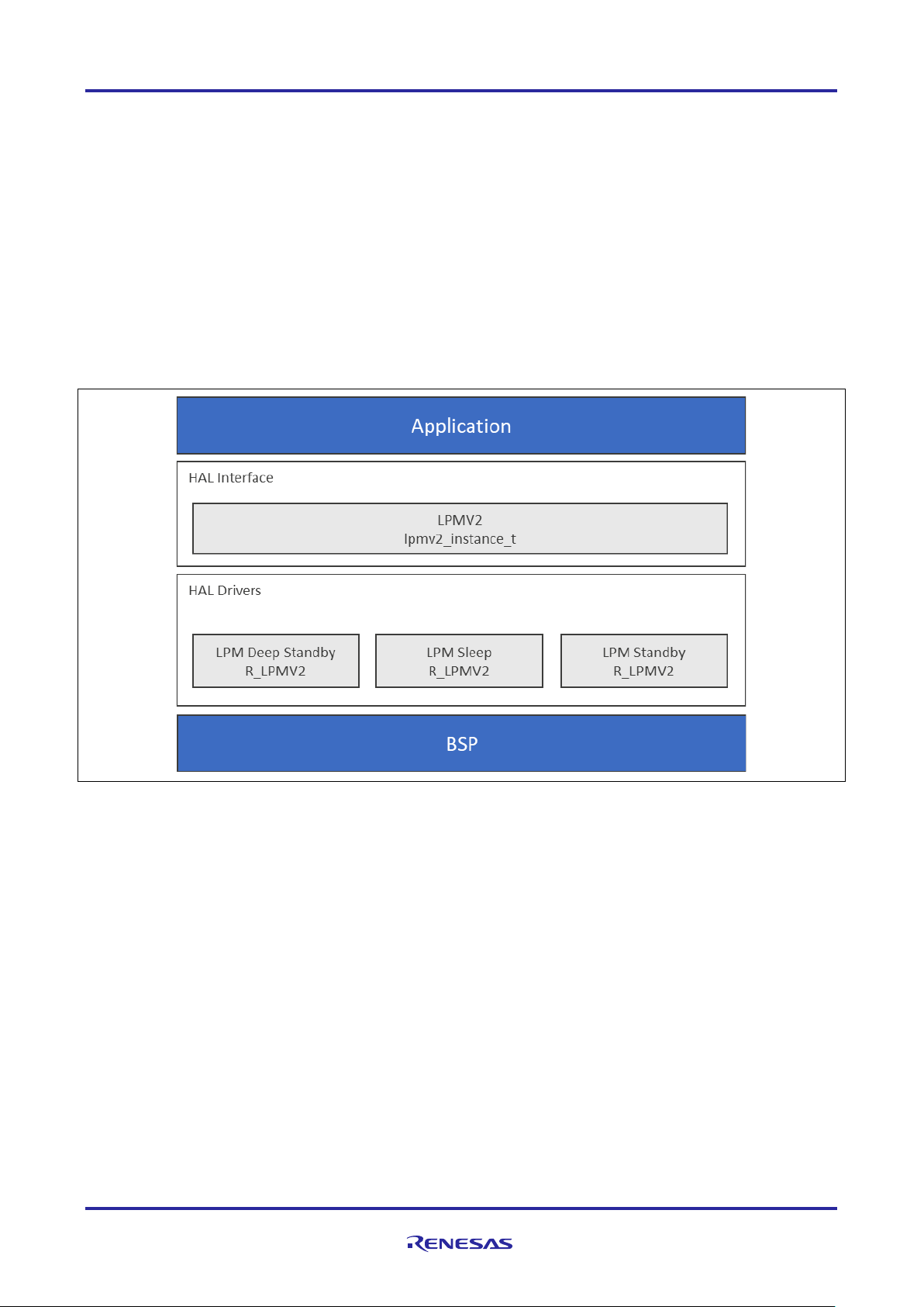
1. Low Power Modes V2 HAL Module Features
The LPM V2 HAL module supports configuration of MCU operating power-control modes and MCU lowpower modes using the low-power mode hardware peripheral.
The LPM V2 HAL module supports the following low power modes:
• Deep Software Standby mode
• Software Standby mode
• Sleep mode
• Snooze mode
The LPM V2 HAL module supports reducing power consumption when in deep stand-by mode through
internal power-supply control and by resetting the states of I/O ports. The LPM V2 HAL module supports
disabling and enabling of the MCU’s other hardware peripherals.
Note: Not all low-power V2 modes are available on all MCUs Groups.
Figure 1. Low Power Modes V2 Module Block Diagram
2. Low Power Modes V2 HAL Module APIs Overview
The Low Power Modes V2 HAL module defines APIs for configuring o perations and enabling and disabling
low-power operations . A complete list of the availa ble APIs, an example API call a nd a short description of
each can be found in the following table. A table of return status values follows the API summary table.
Note: The Low Power Modes V2 HAL module will no longer handle operating power-control modes of the
MCU, these are now handled by the CGC HAL module.
The following API examples illustrate sleep-mode use; “deep_standby” and “standby” can be substituted for
“sleep” in the API examples to create examples for those modes.
R11AN0126EU0102 Rev.1.02 Page 2 of 19
Feb.08.19
Page 3

Renesas Synergy™ Platform Low Power Modes V2 HAL Module Guide
Function Name
Example API Call and Description
.init
g_lpmv2_sleep0.p_api->init(g_lpmv2_sleep0.p_cfg);
in config structure.
.lowerPowerCfg
g_lpmv2_sleep0.p_api->lowerPowerCfg(power_mode,
.lowPowerModeEnter
g_lpmv2_sleep0.p_api->lowPowerModeEnter(void);
.versionGet
g_lpmv2_sleep0.p_api->versionGet(&version);
Get the driver version and place it at the pointer vers ion.
Name
Description
SSP_SUCCESS
API Call Successful
SSP_ERR_INVALID_POINTER
Pointer is NULL
SSP_ERR_INVALID_MODE
Invalid settings for specified mode
SSP_ERR_INVALID_HW_CONDITION
OPCMTSF and SOPCMTSF flags are not cleared
within internally set timeout.
Table 1. Low Power Modes V2 Module API Summary
Open the LPM driver module Initialized the LPM block according to the passed
output_port_enable, power_supply, io_port_state);
Configure a low power mode.
Enter low power mode (sleep/standby/deep standby) using WFI macro. Function
will return after waking from low power mode.
Note: For details on operation and definitions for the function data structures, typedefs, defines, API data,
API structures, and function variables, review the SSP User’s Manual API References for the
associated module.
Table 2. Status Return Values
Note: Lower-level drivers may return common error codes. Refer to the SSP User’s Manual API References
for the associated module for a definition of all relevant status return values.
3. Low Power Modes V2 HAL Module Opera tional O ver view
LPM V2 Initialization
The LPM V2 API function lpm_v2_api_t::init should be called before calling any other LPM V2 function. The
init function handles initialization of internal variables and locks.
Sleep low-power mode
By default, at power on, sleep mode is enabled as the low-power mode. Sleep mode is the most convenient
low-power mode available, as it does not require any special configuration (other than configuring and
enabling a suitable interrupt or event to wake the MCU from sleep) to return to normal program-execution
mode. Any interrupt wakes the MCU device from sleep low-power mode. The states of the SRAM, the
processor registers, and the hardware peripherals are all maintained in sleep mode, and the time needed to
enter and wake from sleep is minimal. Any interrupt causes the MCU device to wake from sleep mode,
including the Systick interrupt used by the ThreadX
lpm_v2_api_t::init should be called before any other function. The LPM API function,
lpm_v2_api_t::lowPowerCfg, can be used to configure the MCU to use sleep as its low-power mode. The
LPM API function lpm_v2_api_t::lowPowerModeEnter should be used to directly enter sleep mode.
An illustrative code example is available on the LPM_V2 Knowledge Base article, available as described in
the Reference Information section at the end of this document.
Software Standby Mode for LPM V2
®
thread scheduler. The LPM API function
In software-standby mode, the CPU, as well as most of the on-chip peripheral functions and all of the internal
oscillators, are stopped. Retained are the contents of the CPU internal registers and SRAM data, the states of
on-chip peripheral functions and I/O Ports. Software-standby mode allows significant reduction in power
consumption, because most of the oscillators are stopped in this mode. Like sleep mode, standby mode
requires an interrupt or event be configured and enabled to wake from standby mode.
R11AN0126EU0102 Rev.1.02 Page 3 of 19
Feb.08.19
Page 4

Renesas Synergy™ Platform Low Power Modes V2 HAL Module Guide
The possible triggers for waking from standby mode are enumerated in the Properties window for convenience;
multiple triggers can be enabled.
An illustrative code example is available on the LPM_V2 Knowledge Base article, available as described in
the Reference Information section at the end of this document.
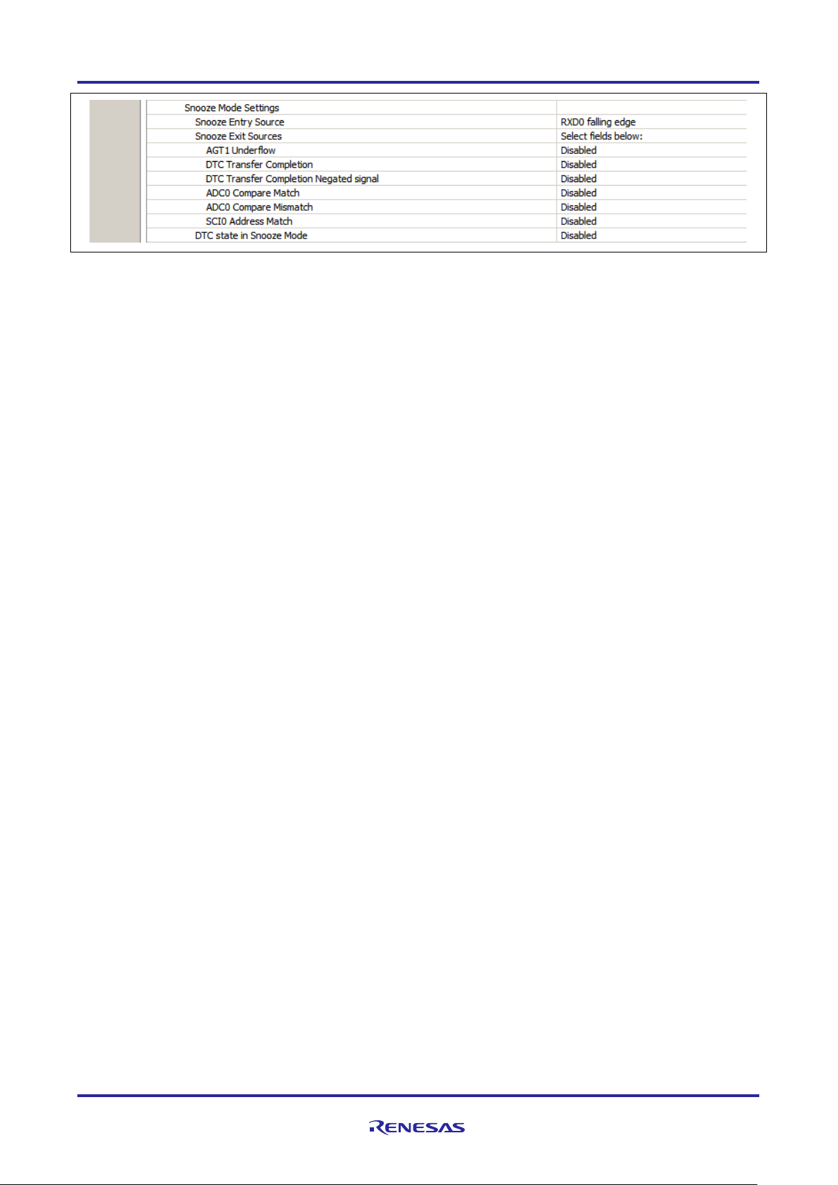
Snooze Mode with Software Standby Mode for LPM V2
Snooze mode is available through the standby mode LPM V2 instance. Choose "Standby with Snooze
Enabled" for “Choose the low power mode” in the Properties window. Snooze mode can be used with some
MCU peripherals to execute basic tasks, while keeping the MCU in a low-power state. The snooze settings
are below the standby settings in the Properties window. The ADC, DTC, and other peripherals can be
enabled in snooze mode. All the settings for snooze are available through configuration properties for the
standby instance, with the exception of the Event Link Controller settings for registers SELSR0 and IELSRn.
Snooze is considered an advanced feature.
The “Snooze Mode Settings” are only used if the low-power mode choice is “Standby with Snooze Enabled,”
as shown in the following screen capture:
Figure 2. Standby mode with Snooze setting enabled
Snooze is a feature of standby mode that allows some peripherals to run even though the MCU core is not
executing instructions. The low-power mode peripheral options related to snooze mode are shown in the
following image. Only one snooze-entry source can be enabled, while multiple snooze-exit sources can be
enabled; the DTC peripheral can be enabled in snooze mode as well.
R11AN0126EU0102 Rev.1.02 Page 4 of 19
Feb.08.19
Page 5
Renesas Synergy™ Platform Low Power Modes V2 HAL Module Guide
Figure 3. Snooze Mode Settings
Deep Software Standby Mode for LPM V2
Deep Softwar e Sta ndb y Mode is onl y a vailabl e on s om e MCU de vices. T he MC U de vice a lwa ys wak es f rom
Deep Software Standby Mode by going through reset, either by the negation of the reset pin or by one of a set
of wake-up events displayed in the configuration Properties window for the LPM deep standby instance.
The possible triggers for waking from deep standby mode are enumerated in the Properties window for
convenience. Multipl e triggers can be enabled. Some triggers ha ve an ass oc iat ed edg e type, falling or ri sing.
These options are enumerated also as shown above and below.
An illustrative code example is available on the LPM_V2 Knowledge Base article, available as described in
the Reference Information section at the end of this document.
3.1 Low Power Modes V2 HAL Module Important Operational Notes and Limitations
3.1.1 Low Power Modes V2 HAL Module Operational Notes
Using this driver to configure the LPM peripheral to wake the MCU from standby mode through interrupts
requires the interrupt to be configured and enabled by the peripheral driver or framework that uses that
interrupt. For example, to wake from standby through AGT1 underflow, that interrupt must be enabled
through the configuration of the AGT timer module.
If the main oscillator or PLL with main-oscillator source is used for the system clock, the wake time from
standby mode can be affected by the Main Oscillator Wait Time Setting in the MOSCWTCR register. This
register setting is available to be changed through the Main Oscillator Wait Time setting in the CGC HAL
module properties. See the Wakeup Timing and Duration table in Electrical Characteristics for more
information.
Note: When a project uses ThreadX and the low-power mode standby, deep standby or standby with
snooze enabled, the call to the lpm_v2_api_t::lowPowerCfg API function should occur immediately
before the call to the lpm_v2_api_t::lowPowerModeEnter API function. This is necessary since
ThreadX also uses low-power modes in its idle loop and tx_thread_sleep function; ThreadX
expects the MCU device to be configured for the low-power mode sleep.
When a project uses ThreadX and the low-power mode standby or standby with snooze enabled, the
low-power mode should be reverted to sleep after the MCU device wakes from standby after returning
from the lpm_v2_api_t::lowPowerModeEnter function. This is necessary since ThreadX also uses
low-power modes in its idle loop and tx_thread_sleep function; ThreadX expects the MCU device
to be configured for the low-power mode sleep. The API function lpm_v2_api_t::lowPowerCfg needs
to be called again before lpm_v2_api_t::lowPowerModeEnter to re-configure the low-power mode to
sleep, if the tx_thread_sleep function is used in the project, or if there may not always be a
thread ready to run.
Detailed information about the expected power consumption of the MCU device in operating states and in
Low Power Modes V2 can be found in the Operating and Standby Current section within the Elec tric al
Characteristics section of the MCU Synergy Hardware User’s Manual.
R11AN0126EU0102 Rev.1.02 Page 5 of 19
Feb.08.19
Page 6
Renesas Synergy™ Platform Low Power Modes V2 HAL Module Guide
Resource
ISDE Tab
Stacks Selection Sequence
g_lpmv2_deep_standby0 S7G2 Low
Threads
New Stack> Driver> Power> Low Power
g_lpmv2_sleep0 S7G2 Low Pow er
Threads
New Stack> Driver> Power> Low Power
g_lpmv2_standby0 S7G2 Low Power
Threads
New Stack> Driver> Power> Low Power
3.1.2 Low Power Modes V2 HAL Module Limitations
• Flash stop (code flash disable) is not supported. See the section “Flash Operation Control Register
(FLSTOP)” of the S1/S3 Synergy Hardware User’s Manual.
• Reduced SRAM retention area in software standby mode is not supported. See the section “Power Save
Memory Control Register (PSMCR)” of the S3 Synergy Hardware User’s Manual.
• The MCU may not enter or stay in Software Standby and Deep Software Standby modes with the
debugger attached. Instead , the MCU ma y be woken fr om Software Standby and Deep Software Stand b y
modes by the debugger. To properly test and verify Software Standby and Deep Software Standby
modes, the debugger must not be attached.
2
(NOTE: Due to some issues, the Application project works only when connected to debugger for e
2
studio. So. while using e
studio, use the application project along with debugger connected to test the
low power modes.).
• If the main oscillator or PLL with the main oscillator source is used for the system clock, the wake time
from standby mode can be affected by the Main Oscillator Wait Time Setting in the MOSCWTCR register.
This register setting can be changed through the Main Oscillator Wait Time setting in the CGC HAL
module properties. See the “Wakeup Timing and Duration” table in Electrical Characteristics for more
information.
• Refer to the latest SSP Release Notes for any additional operational limitations for this module.
4. Including the Low Power Modes V2 HAL Module in an Application
This section describes how to include the Low Power Modes V2 HAL module in an application using the SSP
configurator.
Note: It is assumed you are familiar with creating a project, adding threads, adding a stack to a thread and
configuring a block within the stack. If you are unfamiliar with any of these items, refer to the first few
sections of the SSP User’s Manual to learn how to manage each of these important steps in creating
SSP-based applications.
To add a Low Power Modes V2 Driver to an application, simply add it to a thread using the stacks selection
sequence given in the following table. (The default name for the Low Power Modes Driver is
g_lpmv2_<mode>0. This name can be changed in the associated Properties window.)
Table 3. Low Power Modes V2 Module Selection Sequence
Power Mode Sleep on r_lpmv2
Mode Sleep on r_lpmv2
Mode Sleep on r_lpmv2
Mode Deep Standby on r_lpmv2
Mode Sleep on r_lpmv2
Mode Standby on r_lpmv2
Note: The selection sequences list modes available for the S7G2 Group. Other MCUs will have a different
selection sequence available in the ISDE.
If you add the LPM V2 HAL module to more than one thread, or to a thread and to HAL/Common, give each
instance of the LPM V2 Driver a unique name by highlighting the instance of the driver in the Modules
window and changing the entry for name in the Properties view. The default settings for the LPM V2 HAL
module configuration structure can also be changed using this view.
(The following figure shows the three available low power modes for the S7G2 MCU. These modules can be
added individually or in groups. This figure shows all three for completeness; the c onf igurat or automatically
adds any needed lower-level modules. Modul es with a Gray band are individual modules that stand alone.
Modules with a Blue band are shared or common and need only be added once and can be used by multiple
stacks.
R11AN0126EU0102 Rev.1.02 Page 6 of 19
Feb.08.19
Page 7

Renesas Synergy™ Platform Low Power Modes V2 HAL Module Guide
ISDE Property
Value
Description
Parameter Checking
BSP, Enabled, Disabled
(Default: BSP)
Enables or disables the
Name
g_lpmv2_deep_standby0
Module name
Output port state in
control output pins
High impedance state, No change (Default:
Output port state setting in
Maintain or reset the IO
deep standby mode
Maintain the IO port states, Reset the IO port
Output port state setting exit
Internal power supply
Maintain the internal power supply, Cut the
(Default: Maintain the internal po wer supp l y)
Internal power supply control
Figure 4. Low Power Modes V2 Module Stack
5. Configuring the Low Powe r Modes V2 HAL Module
The Low Power Modes V2 Driver module must be configured by the user for the desired operation. The SSP
configuration window auto matically identifies (by highlighting the block in red) any required configuration
selections, such as interrupts or operating modes, which must be configured for lower-level modules for
successful operation. Only those properties that can be changed without causing conflicts are available for
modification. Other properties are ‘locked’ and are not available for changes, and are identified with a lock
icon for the ‘locked’ property in the Properties window in the ISDE. This approach simplifies the configuration
process and makes it much less error-prone than previous ‘manual’ approaches to configuration. The
available configuration settings and defaults for all the user-accessible properties are given in the properties
tab within the SSP configurator and are shown in the following tables for easy reference.
One of the properties most often identified as requiring a change is the interrupt priority; this configuration
setting is available within the Properties window of the associated module. Simply select the indicated
module and then view the Properties window; the interrupt settings are often toward the bottom of the
properties list, so scroll down until they become available. Also note that the interrupt priorities listed in the
Properties window in the ISDE includes an indication as to the validity of the setting based on the targeted
MCU (CM4 or CM0+). This level of detail is not included in the following configuration properties tables, but
is easily visible within the ISDE when configuring interrupt-priority leve ls .
Note: You may want to open your ISDE, create the module and explore the property settings in parallel with
looking over the following configuration table settings. This helps orient you and can be a useful
‘hands-on’ approach to learning the ins and outs of developin g with SS P.
Table 4. Configuration Settings for the Low Power Mode Deep Standby Module on r_lpmv2
parameter checking
standby and deep
standby, applies to
address output, data
output, and other bus
port states on exit from
No change)
states (Default: Maintain the IO port states)
Standby and Deep Standby
control in deep standby
mode
R11AN0126EU0102 Rev.1.02 Page 7 of 19
Feb.08.19
power supply to standby RAM, low-speed onchip oscillator, AGTn, and USBFS/HS resume
detecting unit, Cut the power supply to LVDn,
standby RAM, low-speed on-chip oscillator,
AGTn, and USBFS/HS resume detecting unit
in deep standby mode setting
Page 8

Renesas Synergy™ Platform Low Power Modes V2 HAL Module Guide
ISDE Property
Value
Description
Deep Standby Cancel Sources /Edges : Se lect F ie lds Belo w
IRQ0
Enabled, Disabled (Default: Disabled)
IRQ0 selection
IRQ0 Edge
Disabled, Rising Edge, Falling Edge (Default:
Disabled)
IRQ0 Edge selection
IRQ1
Enabled, Disabled (Default: Disabled)
IRQ1 selection
IRQ1 Edge
Disabled, Rising Edge, Falling Edge (Default:
Disabled)
IRQ1 Edge selection
IRQ2
Enabled, Disabled (Default: Disabled)
IRQ2 selection
IRQ2 Edge
Disabled, Rising Edge, Falling Edge (Default:
Disabled)
IRQ2 Edge selection
IRQ3
Enabled, Disabled (Default: Disabled)
IRQ3 selection
IRQ3 Edge
Disabled, Rising Edge, Falling Edge (Default:
Disabled)
IRQ3 Edge selection
IRQ4
Enabled, Disabled (Default: Disabled)
IRQ4 selection
IRQ4 Edge
Disabled, Rising Edge, Falling Edge (Default:
Disabled)
IRQ4 Edge selection
IRQ5
Enabled, Disabled (Default: Disabled)
IRQ5 selection
IRQ5 Edge
Disabled, Rising Edge, Falling Edge (Default:
Disabled)
IRQ5 Edge selection
IRQ6
Enabled, Disabled (Default: Disabled)
IRQ6 selection
IRQ6 Edge
Disabled, Rising Edge, Falling Edge (Default:
Disabled)
IRQ6 Edge selection
IRQ7
Enabled, Disabled (Default: Disabled)
IRQ7 selection
IRQ7 Edge
Disabled, Rising Edge, Falling Edge (Default:
Disabled)
IRQ7 Edge selection
IRQ8
Enabled, Disabled (Default: Disabled)
IRQ8 selection
IRQ8 Edge
Disabled, Rising Edge, Falling Edge (Default:
Disabled)
IRQ8 Edge selection
IRQ9
Enabled, Disabled (Default: Disabled)
IRQ9 selection
IRQ9 Edge
Disabled, Rising Edge, Falling Edge (Default:
Disabled)
IRQ9 Edge selection
IRQ10
Enabled, Disabled (Default: Disabled)
IRQ10 selection
IRQ10 Edge
Disabled, Rising Edge, Falling Edge (Default:
Disabled)
IRQ10 Edge selection
IRQ11
Enabled, Disabled (Default: Disabled)
IRQ11 selection
IRQ11 Edge
Disabled, Rising Edge, Falling Edge (Default:
Disabled)
IRQ11 Edge selection
IRQ12
Enabled, Disabled (Default: Disabled)
IRQ12 selection
IRQ12 Edge
Disabled, Rising Edge, Falling Edge (Default:
Disabled)
IRQ12 Edge selection
IRQ13
Enabled, Disabled (Default: Disabled)
IRQ13 selection
IRQ13 Edge
Disabled, Rising Edge, Falling Edge (Default:
Disabled)
IRQ13 Edge selection
IRQ14
Enabled, Disabled (Default: Disabled)
IRQ14 selection
IRQ14 Edge
Disabled, Rising Edge, Falling Edge (Default:
Disabled)
IRQ14 Edge selection
IRQ15
Enabled, Disabled (Default: Disabled)
IRQ15 selection
IRQ15 Edge
Disabled, Rising Edge, Falling Edge (Default:
Disabled)
IRQ15 Edge selection
LVD1
Enabled, Disabled (Default: Disabled)
LVD1 selection
R11AN0126EU0102 Rev.1.02 Page 8 of 19
Feb.08.19
Page 9
Renesas Synergy™ Platform Low Power Modes V2 HAL Module Guide
ISDE Property
Value
Description
LVD1 Edge
Disabled, Rising Edge, Falling Edge (Default:
Disabled)
LVD1 Edge selection
LVD2
Enabled, Disabled (Default: Disabled)
LVD2 selection
LVD2 Edge
Disabled, Rising Edge, Falling Edge (Default:
Disabled)
LVD2 Edge selection
RTC Interval
Enabled, Disabled (Default: Disabled)
RTC Interval selection
RTC Alarm
Enabled, Disabled (Default: Disabled)
RTC Alarm selection
NMI
Enabled, Disabled (Default: Disabled)
NMI selection
NMI Edge
Disabled, Rising Edge, Falling Edge (Default:
Disabled)
NMI Edge selection
USBFS
Enabled, Disabled (Default: Disabled)
USBFS selection
UBSHS
Enabled, Disabled (Default: Disabled)
UBSHS selection
AGT1
Enabled, Disabled (Default: Disabled)
AGT1 selection
ISDE
Property
Value
Description
Parameter
BSP, Enabled, Disabled
(Default: BSP)
Enables or disables the parameter checking
Name
g_lpmv2_sleep0
Module name
ISDE Property
Value
Description
Parameter Checking
BSP, Enabled, Disabled
(Default: BSP)
Enables or disables the
Name
g_lpmv2_standby0
Module name
Choose the low power mode
Standby, Standby with Snooze
(Default: Standby)
Low power mode
Output port state in standby and
No Change, High Impedance state
Output port state
Select Standby Exit Sources: Select Fi elds bel o w
IRQ0:15
Enabled, Disabled
IRQ0:16 selection
IWDT
Enabled, Disabled
(Default: Disabled)
IWDT selection
Key Interrupt
Enabled, Disabled
Key Interrupt selection
LVD1 Interrupt
Enabled, Disabled
(Default: Disabled)
LVD1 selection
LVD2 Interrupt
Enabled, Disabled
(Default: Disabled)
LVD2 selection
Note: The example values and defaults are for a project using the Synergy S7G2 MCU Family. Other MCUs
may have different default values and available configuration settings.
Table 5. Configuration Settings for Low Power Mode Sleep Driver on r_lpmv2
Checking
Note: The example values and defaults are for a project using the Synergy S7G2. Other MCUs may have
different default values and available configuration settings.
Table 6. Configuration Settings for Low Power Mode Standby Driver on r_lpmv2
parameter checking
selection
selection
deep standby, applies to address
output, data output, and other bus
control pins
enabled
(Default: No Change)
(Default: Disabled)
R11AN0126EU0102 Rev.1.02 Page 9 of 19
Feb.08.19
(Default: Disabled)
Page 10

Renesas Synergy™ Platform Low Power Modes V2 HAL Module Guide
ISDE Property
Value
Description
Analog Comparator High-speed 0
Enabled, Disabled
(Default: Disabled)
Analog Comparator
RTC Period
Enabled, Disabled
RTC Period selection
RTC Alarm
Enabled, Disabled
(Default: Disabled)
RTC Alarm selection
USBFS
Enabled, Disabled
(Default: Disabled)
USBFS selection
UBSHS
Enabled, Disabled
(Default: Disabled)
UBSHS selection
AGT1 underflow
Enabled, Disabled
AGT1 underflow selection
AGT1 Compare Match A
Enabled, Disabled
(Default: Disabled)
AGT1 CMA selection
AGT1 Compare Match B
Enabled, Disabled
AGT1 CMB selection
I2C 0
Enabled, Disabled
(Default: Disabled)
I2C 0 selection
Snooze Mode Settings
Snooze Entry Source
RXD0 falling edge, IRQ0:15, KINT
(Default: RXD0 falling edge)
Source of Snooze mode
Snooze Exit Sources: Select fields below
AGT1 Underflow
Enabled, Disabled
(Default: Disabled)
AGT1 Underflow
DTC Transfer Completion
Enabled, Disabled
DTC Transfer Completion
DTC Transfer Completion Negated
Enabled, Disabled
(Default: Disabled)
DTC Transfer Completion
ADC0 Compare Match
Enabled, Disabled
ADC0 Compare Match
ADC0 Compare Mismatch
Enabled, Disabled
(Default: Disabled)
ADC0 Compare
ADC1 Compare Match
Enabled, Disabled
(Default: Disabled)
ADC1 Compare Match
ADC1 Compare Mismatch
Enabled, Disabled
(Default: Disabled)
ADC1 Compare
SCI0 Address Match
Enabled, Disabled
SCI0 Address Match
DTC State Selection
DTC state in Snooze Mode
Enabled, Disabled
DTC state in Snooze
Interrupt
(Default: Disabled)
(Default: Disabled)
(Default: Disabled)
(Key Interrupt), ACMPHS0 (H ighspeed Analog Comparator 0), RTC
Alarm, RTC Period, AGT1 Underflow,
AGT1 Compare Match A, AGT1
Compare Match B
selection
entry
signal
Note: The example values and defaults are for a project using the Synergy S7G2. Other MCUs may have
different default values and available configuration settings.
In some cases, settings other than the defaults can be desirable. For example, it might be useful to select
different states for entering or exiting low-power states.
(Default: Disabled)
(Default: Disabled)
(Default: Disabled)
(Default: Disabled)
selection
selection
Negated signal selection
selection
Mismatch selection
selection
Mismatch selection
selection
Mode selection
R11AN0126EU0102 Rev.1.02 Page 10 of 19
Feb.08.19
Page 11

Renesas Synergy™ Platform Low Power Modes V2 HAL Module Guide
5.1 Low Power Modes V2 HAL Module Clock Configuration
The Low Power Modes V2 peripheral module does not have any selectable clock sources.
5.2 Low Power Modes V2 HAL Module Pin Configuration
The Low Power Modes V2 peripheral module needs no pin assignments. Pin function selections are done in
the properties configuration window.
6. Using the Low Power Modes V2 H AL Module in an Application
The typical steps in using the Low Power Modes V2 HAL module in an application are:
1. Initialize the Low Power Modes V2 HAL module using the lpm_v2_api_t::init API
2. Configure a low-power mode with the lpm_v2_api_t::lowPowerCfg API
3. Enter a low-power mode with the lpm_v2_api_t::lowPowerModeEnter API
These common steps are illustrated in a typical operational flow diagram in the following figure:
Figure 5. Flow Diagram of a Typical Low Power Modes V2 Module Application
7. The Low Power Modes V2 HAL Module Application Project
The application project associated with this module guide demonstrates the configuration steps in an
example application. You may want to import and open the application project within the ISDE and view the
configuration settings for the Low Power Modes V2 HAL module. You can also review the code (in
lpm_v2_hal_module_guide_project.c) which demonstrates the Low Power Modes HAL module APIs
in a complete design.
The application project demonstrates the typical use of the Low Power Modes HAL module APIs. The
application project demonstration function initializes LEDs and the necessary lower-level modules: the
External IRQ HAL module, RTC HAL module and selected Low Power Mode HAL module. When the Deep
Software Standby Mode is chosen, there is an additional check, because leaving this mode causes the
device to reset.
After the amber LED illuminates, the selected low-power mode is configured and the RTC counter is started.
The green LED blinks and the device enters low-power mode. In sleep mode, the device generally wakes on
any interrupt. Settings for Software Standby and Deep Software Standby modes specify interrupts from
which low-power mode can exit. The application makes use of two interrupts: IRQ11 (S4 push button) and
the RTC Period.
When the user presses the S4 button, the previously configured external interrupt is executed, and its
service routine is called. The RTC HAL module is configured to emit a period interrupt every two seconds.
When the device wakes up, due to the IRQ11 interrupt, the red LED illuminates; when it wakes from the RTC
Period interrupt, the green LED blink s . The service routines for these interrupts do not execute when the
device enters Deep Software Standby mode.
R11AN0126EU0102 Rev.1.02 Page 11 of 19
Feb.08.19
Page 12
Renesas Synergy™ Platform Low Power Modes V2 HAL Module Guide
Resource
Revision
Description
e2 studio
6.2.1 or later
Integrated Solution Development Environment
SSP
1.5.0 or later
Synergy Software Platform
IAR EW for Renesas
Synergy
SSC
6.2.1 or later
Synergy Standalone Configurator
SK-S7G2
v3.0 to v3.1
Starter Kit
Table 7. Software and Hardware Resources Used by the Application Project
8.23.1 or later IAR Embedded Workbench® for Renesas Synergy™
The following two flow diag r am s illustrate the modes available in a simple Application project.
Figure 6. Low Power Modes V2 Module Application Project Flow Diagram (Sleep and Software
Standby modes)
R11AN0126EU0102 Rev.1.02 Page 12 of 19
Feb.08.19
Page 13

Renesas Synergy™ Platform Low Power Modes V2 HAL Module Guide
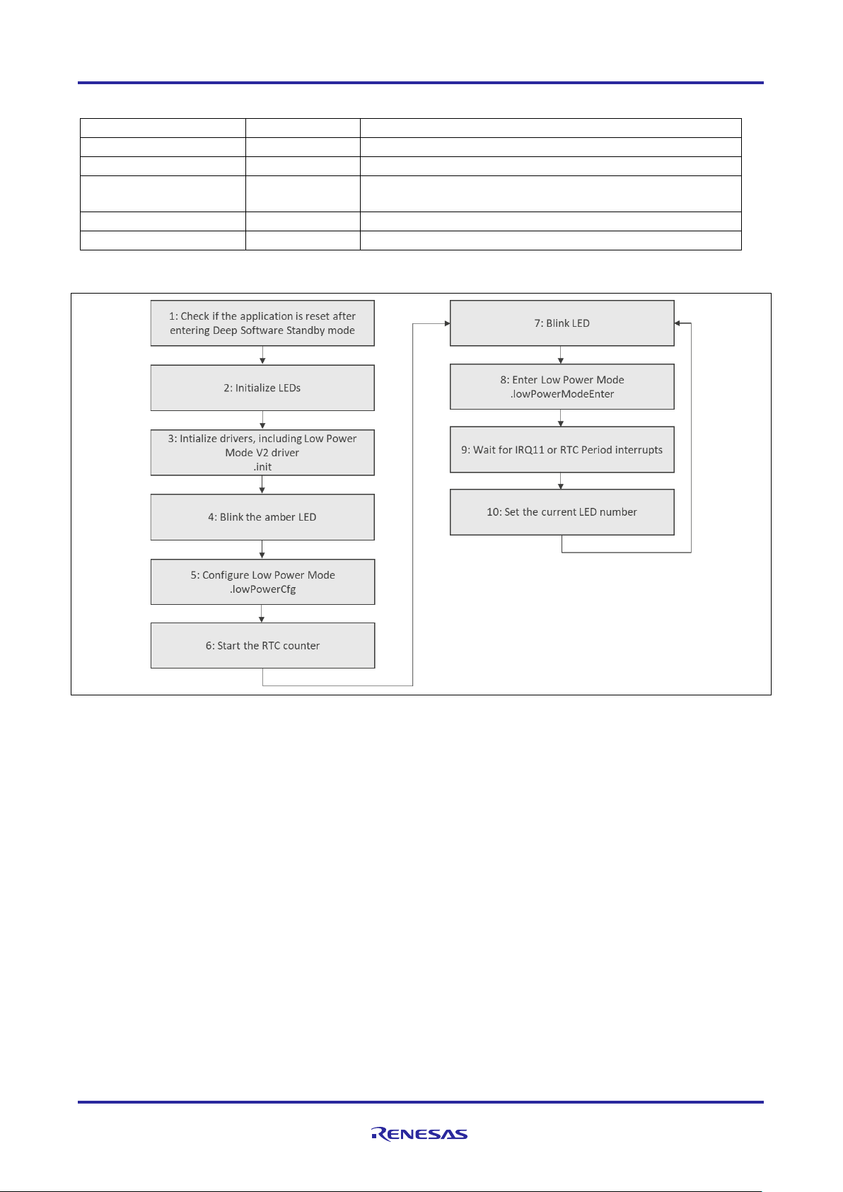
Figure 7. Low Power Modes V2 Module Application Project Flow Diagram (Deep Software Standby
mode)
The lpm_v2_hal_module_guide_project.c file is located in the project once it has been imported into
the ISDE. You can open this file within the ISDE and follow along with the description provided to help
identify key uses of APIs.
The first section of lpm_v2_hal_module_guide_project.c has the header files which reference the
LPM instance structure. Next, some macro constants are defined. The LPM_MODE definition should be
used to select the low-power mode. After this definition, there are other macros which help to run the
application project on other Synergy boards. The next section has function prototypes, and their bodies
follow. The first one is used for LED initialization; it gets the BSP LED information and checks if there are at
least two LEDs and turns off all the LEDs. The second function initializes the External IRQ HAL module (for
S4 button handling), RTC HAL module, and Low Power Modes V2 HAL module. The third function checks if
the device has just left Deep Software Standby mode and clears the flags in Deep Software Standby mode
registers.
The next section is the entry function for the main program-control section. The necessary initialization is
performed, and the selected Low Power Mode is configured. Inside the ‘forever’ while loop, the currently set
LED blinks, and the low-power mode is entered and waits for an interrupt. After waking up, the while loop
functions are repeated.
The last section contains callback functions for the IRQ11 and RTC Period interrupts; they change the
current LED number. When the execution of this callback ends, the MCU is awake.
(Note that when Deep Software Standby mode is used and one of the configured interrupts occur, the device
will be reset and hence the callback will not be called.)
Since the application project uses low-power modes, some options must be set in order to provide handling
of these modes when debugging. Otherwise, the device will always enter sleep mode regardless of the
selected mode, and after entering low-power mode, the debug connection can be lost.
2
In the e
studio Integrated Solution Development Environment (ISDE), perform the following steps to change
settings:
1. Select the project as active and choose Run > Debug Configurations.
2. Mark a project-related debug configuration on the left and select the Debugger tab on the right.
3. Go to the Connection Settings tab.
R11AN0126EU0102 Rev.1.02 Page 13 of 19
Feb.08.19
Page 14
Renesas Synergy™ Platform Low Power Modes V2 HAL Module Guide
ISDE Property
Value Set
Parameter Checking
Default (BSP)
Name
g_lpmv2_sleep
ISDE Property
Value Set
Parameter Checking
Default (BSP)
Name
g_lpmv2_standby
Choose the low power mode
Standby
Output port state in standby and deep standby,
bus control output pins
No change
Select Standby Exit Sources: Select fields below
IRQ0:10
Disabled
IRQ11
Enabled
IRQ12:15
Disabled
IWDT, Key Interrupt, LVD1:2 Interrupt, Analog
Disabled
RTC Period
Enabled
USB High-speed, USB Full-speed, AGT1
Disabled
Snooze Mode Settings
Snooze Entry Source
RXD0 falling edge
Snooze Exit Sources: Select fields below
AGT1 Underflow, DTC Transfer Completion, DTC
Disabled
DTC state in Snooze Mode
Disabled
4. In Script File, setting select the CM_low_power_debug.JLinkScript script attached with the application
project. (It is important that the path to this script does not contain any space.)
5. Set Yes in the Low-Power Handling setting.
In IAR Embedded Workbench
1. Select the project as active and choose Project > Options.
2. Select Debugger on the left sidebar and the Setup tab on the right.
3. Check Use macro file(s) and select the low_power_debug.mac file attached with the application
project.
4. Open the settings/LPM_V2_HAL_MG_AP_Debug.jlink file.
If the file does not exist, attach the debugger to the device and disconnect. The file is created when
attaching to the device for the first time.
5. Change the following line:
LowPowerHandlingMode = 0 to: LowPowerHandlingMode = 1
6. Save the file.
A few key properties configured in this application project support the required operations and the physical
properties of the target board and MCU device. The following tables list properties with values set for this
specific project. You can also open the application project and view these settings in the Properties window
as a hands-on exercise.
Table 8. Low Power Mode V2 Sleep Module Configuration Settings for the Application Project
®
for Renesas Synergy™ perform the following steps to change settings:
Table 9. Low Power Mode V2 Standby Module Configuration Settings for the Application Project
applies to address output, data output, and other
Comparator High-speed 0 Interrupt, RTC Alarm
underflow, AGT 1 Compare Match A/B, I2C 0
Transfer Completion Negated signal, ADC0
Compare Match, ADC0 Compare Mismatch,
ADC1 Compare Match, ADC1 Compare
Mismatch, SCI0 Address Match
R11AN0126EU0102 Rev.1.02 Page 14 of 19
Feb.08.19
Page 15

Renesas Synergy™ Platform Low Power Modes V2 HAL Module Guide
ISDE Property
Value Set
Parameter Checking
Default (BSP)
Name
g_lpmv2_deep_standby
Choose the low power mode
Standby
Output port state in standby and deep standby,
No change
Maintain or reset the IO port states on exit from
deep standby mode
Maintain the IO port states
Deep Standby Cancel Sources /Edges : Se lect fields below
IRQ0:10
Disabled
IRQ11
Enabled
IRQ11 edge
Rising edge
IRQ12:15
Disabled
LVD1:2
Disabled
RTC Interval
Enabled
RTC Alarm, NMI, USBFS, USBHS, AGT1
Disabled
ISDE Property
Value Set
Parameter Checking Enable
Default (BSP)
Name
g_rtc
Clock Source
LOCO
Error Adjustment Value [DEPRECATED]
0
Error Adjustment Type [DEPRECATED]
None
Callback
rtc_callback
Alarm Interrupt Priority
Disabled
Period Interrupt Priority
Priority 5 (CM4: valid, CM0+: invalid)
Carry Interrupt Priority
Disabled
ISDE Property
Value Set
Parameter Checking
Default (BSP)
Name
g_external_irq11
Channel
11
Trigger
Rising
Digital Filtering
Enabled
Digital Filtering Sample Clock
PCLK / 64
Interrupt enabled after initialization
True
Callback
irq11_callback
Interrupt Priority
Priority 5 (CM4: valid, CM0+: invalid)
Table 10. Low Power Mode V2 Deep Standby Module Configur ation Settings for the A pplication Project
applies to address output, data output, and other
bus control output pins
Table 11. RTC Driver Module Configuration Settings for the Appli cation Project
Table 12. External IRQ Driver Module Configuration Settings for the Application Project
8. Customizing the Low Pow er Modes V2 HAL Module for a Target Application
Some configuration setti ngs will normally be change d by the developer fr om those shown in the applicati on
project. For example, the user may configure different exit sources for Standby or Deep Standby modes.
To help with customization efforts, examples of specific low power applications are available on the LPM_V2
Knowledge Base article, available as described in the Reference Information section at the end of this
document.
R11AN0126EU0102 Rev.1.02 Page 15 of 19
Feb.08.19
Page 16

Renesas Synergy™ Platform Low Power Modes V2 HAL Module Guide
9. Running the Low Power Modes V2 HAL Module Application Project
To run the Low Power Modes V2 HAL module application project and to see it executed on a target kit, you
can simply import it into your ISDE, compile and run debug. Refer to the Synergy Project Import Guide
(r11an0023eu0121-synergy-ssp-import-guide.pdf), included in this package for instructions on importing the
project into e
To implement the Low Power Modes application in a new project, use the following steps for defining,
configuring, auto-gener ating files, adding code, compil ing and debugg ing on the target kit. The steps offer a
hands-on approach that helps to make the development process with SSP more practical.
Note: The tasks are given in s uf f ic ient deta il for someone experienced with the basic flow through the
To create and run the Low Power Modes V2 HAL module application project, follow these steps:
1. Create a new Renesas Synergy project for the S7G2-SK called LPM_V2_HAL_MG_AP.
2. Select the Threads tab.
3. Add the External IRQ HAL module to the HAL/Common thread.
4. Add the S7G2 Low Power Mode Sleep Driver to the HAL/Common thread.
5. Configure the added blocks according to the preceding tables.
6. Click on the Generate Project Content button.
7. Add the code from supplied project files: hal_entry.c, lpm_v2_hal_module_guide_project.c ,
and lpm_v2_hal_module_guide_project.h. Alternatively, copy over the generated
hal_entry.c, lpm_v2_hal_module_guide_project.c , and
lpm_v2_hal_module_guide_project.h files.
8. Select low-power mode in the lpm_v2_hal_module_guide_project.c file using the LPM_MODE
macro.
9. Enable low-power modes handling in the editor by following the preceding instructions.
10. Connect to the host PC using the USB cable (use J19 DEBUG_USB connector).
11. Start to debug the application.
12. The output can be viewed on onboard LEDs. Use S4 button to blink an LED.
2
studio ISDE or the IAR EW for Synergy, and then building/running the application.
Synergy development process. If these steps are not familiar, refer to the first few chapters of the
SSP User’s Manual for a description of how to accomplish these steps.
Figure 8. Example Output from the Low Power Modes V2 Module Appli cation Project
R11AN0126EU0102 Rev.1.02 Page 16 of 19
Feb.08.19
Page 17

Renesas Synergy™ Platform Low Power Modes V2 HAL Module Guide
10. Low Power Modes V2 HAL Module Conclusion
This module guide has pr ovided a ll the b ack ground inf orm ation nee ded to s elect, add, conf igure an d use th e
module in an example project. Many of these steps were time consuming and error-prone activities in previous
generations of embedded systems. The Renesas Synergy Platform makes these steps much less time
consuming and removes the common errors, like conflicting configuration settings or the incorrect selection of
lower-level drivers. The use of high-level APIs (as demonstrated in the application project) illustrates additional
development time s avings by allowing work to begin at a high level and avoiding the t ime required in older
development environments to use or, in some cases, create, lower-level drivers.
11. Low Power Modes V2 HAL Module Next Steps
After you have mastered a simple Low Power Modes V2 HAL module project, you may want to review a
more complex example. You may find that disabling the clocks is necessary; the CGC HAL module is able to
reconfigure or switch the clocks on and off. The module guide for the CGC HAL module is available to
download, simply follow the instructions in the References section at the end of this document.
12. Low Power Modes V2 HAL Module Reference Information
SSP User Manual: Available in HTML format at www.renesas.com/us/en/products/synergy/software/ssp.html
as a SSP distribution package, and also as a pdf from the Synergy Gallery.
Links to all the most up-to-date r_lpm2 module reference materials and resources are available on the
Synergy Knowledge Base: https://en-support.renesas.com/knowledgeBase/16977494
R11AN0126EU0102 Rev.1.02 Page 17 of 19
Feb.08.19
Page 18

Renesas Synergy™ Platform Low Power Modes V2 HAL Module Guide
Website and Support
Visit the following vanity URLs to learn about key elements of the Synergy Platform, download components
and related documentation, and get support.
Synergy Software www.renesas.com/synergy/software
Synergy Software Package www.renesas.com/synergy/ssp
Software add-ons www.renesas.com/synergy/addons
Software glossary www.renesas.com/synergy/softwareglossary
Development tools www.renesas.com/synergy/tools
Synergy Hardware www.renesas.com/synergy/hardware
Microcontrollers www.renesas.com/synergy/mcus
MCU glossary www.renesas.com/synergy/mcuglossary
Parametric search www.renesas.com/synergy/parametric
Kits www.renesas.com/synergy/kits
Synergy Solutions Gallery www.renesas.com/synergy/solutionsgallery
Partner projects www.renesas.com/synergy/partnerprojects
Application projects www.renesas.com/synergy/applicationprojects
Self-service support resources:
Documentation www.renesas.com/synergy/docs
Knowledgebase www.renesas.com/synergy/knowledgebase
Forums www.renesas.com/synergy/forum
Training www.renesas.com/synergy/training
Videos www.renesas.com/synergy/videos
Chat and web ticket www.renesas.com/synergy/resourcelibrary
R11AN0126EU0102 Rev.1.02 Page 18 of 19
Feb.08.19
Page 19

Renesas Synergy™ Platform Low Power Modes V2 HAL Module Guide
Rev.
Date
Description
Page
Summary
1.00
Jun.08.17
Initial version
1.01
Aug.23.17
Update to Hardware and Software Resources Table
1.02
Feb.08.19
Updated to SSP v1.5.0
Revision History
R11AN0126EU0102 Rev.1.02 Page 19 of 19
Feb.08.19
Page 20

Corporate Headquarters
Contact information
www.renesas.com
Trademarks
of their respective owners.
Notice
1. Descriptions of circuits, software and other related information in this document are provided only to illustrate the operation of semiconductor products
and application examples. You are fully responsible for the incorporation or any other use of the circuits, software, and information in the design of your
product or system. Renesas Electronics disclaims any and all liabi li t y for any l osses and damages incurred b y you or third parties arising from the use
of these circuits, software, or information.
2. Renesas Electronics hereby expressly disclaims any warranties against and liability for infringement or any other claims involving patents, copyrights,
or other intellectual property rights of third parties, by or arising from the use of Renesas Electronics products or technical information described in this
document, including but not limited to, the product data, drawings, charts, programs, algorithms, and application examples.
3. No license, express, implied or otherwise, is granted hereby under any patents, copyrights or other intellectual property rights of Renesas Electronics
or others.
4. You shall not alter, modify, copy, or reverse engineer any Renesas Electronics product, whether in whole or in part. Renesas Electronics disclaims any
and all liability for any losses or damages incurred by you or third parties arising from such alteration, modification, copying or reverse engineering.
5. Renesas Electronics products are classified according to the following two quality grades: “Standard” and “High Quality”. The intended applications for
each Renesas Electronics product depends on the product’s quality grade, as indicated below.
"Standard": Computers; office equipment; communications equipment; test and measurement equipment; audio and visual equipment; home
"High Quality": Transportation equipment (automobiles, trains, ships, etc.); traffic control (traffic lights); large-scale communication equipment; key
Unless expressly designated as a high reliability product or a product for harsh environments in a Renesas Electronics data sheet or other Renesas
Electronics document, Renesas Electronics products are not intended or authorized for use in products or systems that may pose a direct threat to
human life or bodily injury (artificial life support devices or systems; surgical implantations; etc.), or may cause serious property damage (space
system; undersea repeaters; nuclear power control systems; aircraft control systems; key plant systems; military equipment; etc.). Renesas Electronics
disclaims any and all liability for any damages or losses incurred by you or any third parties arising from the use of any Renesas Electronics product
that is inconsistent with any Renesas Electronics data sheet, user’s manual or other Renesas Electronics document.
6. When using Renesas Electronics products, refer to the latest product information (data sheets, user’s manuals, application notes, “General Notes for
Handling and Using Semiconductor Devices” in the reliability handbook, etc.), and ensure that usage conditions are within the ranges specified by
Renesas Electronics with respect to maximum ratings, operating power supply voltage range, heat dissipation characteristics, installation, etc. Renesas
Electronics disclaims any and all liability for any malfunctions, failure or accident arising out of the use of Renesas Electronics products outside of such
specified ranges.
7. Although Renesas Electronics endeavors to improve the quality and reliability of Renesas Electronics products, semiconductor produc ts hav e s pecifi c
characteristics, such as the occurrence of failure at a certain rate and malfunctions under certain use conditions. Unless designated as a high reliability
product or a product for harsh environments in a Renesas Electronics data sheet or other Renesas Electronics document, Renesas Electronics
products are not subject to radiation resistance design. You are responsible for implementing safety measures to guard against the possibility of bodily
injury, injury or damage caused by fire, and/or danger to the public in the event of a failure or malfunction of Renesas Electronics products, such as
safety design for hardware and software, including but not limited to redundancy, fire control and malfunction prevention, appropriate treatment for
aging degradation or any other appropriate measures. Because the evaluation of microcomputer software alone is very difficult and im pr acti c al, you are
responsible for evaluating the safety of the final products or systems manufactured by you.
8. Please contact a Renesas Electronics sales office for details as to environmental matters such as the environmental compatibility of each Renesas
Electronics product. You are responsible for carefully and sufficiently investigating applicable laws and regulations that regulate the inclusion or use of
controlled substances, including without limitation, the EU RoHS Directive, and using Renesas Electronics products in compliance with al l these
applicable laws and regulations. Renesas Electronics disclaims any and al l lia bil it y for dam a ges or los s es oc cu rri ng a s a result of your no ncom pl i ance
with applicable laws and regulations.
9. Renesas Electronics products and technologies shall not be used for or incorporated into any products or systems whose manufacture, use, or sale is
prohibited under any applicable domestic or foreign laws or regulations. You shall comply with any applicable export control laws and regulations
promulgated and administered by the governments of any countries asserting jurisdiction over the parties or transactions.
10. It is the responsibility of the buyer or distributor of Renesas Electronics products, or any other party who distributes, disposes of, or otherwise sells or
transfers the product to a third party, to notify such third party in advance of the contents and conditions set forth in this document.
11. This document shall not be reprinted, reproduced or duplicated in any form, in whole or in part, without prior written consent of Renesas Electronics.
12. Please contact a Renesas Electronics sales office if you have any questions regarding the information contained in this document or Renesas
Electronics products.
(Note1) “Renesas Electronics” as used in this document means Renesas Electronics Corporation and also includ es its dir ectly or indirectly controlled
(Note2) “Renesas Electronics product(s)” means any product developed or manufactured by or for Renesas Electronics.
subsidiaries.
electronic appliances; machine tools; personal electronic equipment; industrial robots; etc.
financial terminal systems; safety control equipment; etc.
(Rev.4.0-1 November 2017)
TOYOSU FORESIA, 3-2-24 Toyosu,
Koto-ku, Tokyo 135-0061, Japan
Renesas and the Renesas logo are trademarks of Renesas Electronics
Corporation. All trademarks and registered trademarks are the property
For further information on a product, technology, the most up-to-date
version of a document, or your ne are s t sales office, please visit:
www.renesas.com/contact/.
© 2019 Renesas Electronics Corporation. All rights reserved.
 Loading...