

Page 1
HA17458 Series
Dual Operational Amplifier
REJ03D0680-0100
(Previous: ADE-204-0 40)
Rev.1.00
Jun 15, 2005
Description
HA17458 is dual operational amplifiers which provides internal phase compensation and high performance. It can be
applied widely to measur ing contr ol equipment and to general use.
Features
•
High voltage gain: 100dB (Typ)
•
Wide output amplitude: ±13V (Typ) [at R
• Protected from output shortcircuit
•
Internal phase compensation
Ordering Information
Type No. Application Package Code (Previous Code)
HA17485FP Industrial use PRSP0008DE-B (FP-8DGV)
HA17458F Commercial use PRSP0008DE-B (FP-8DGV)
HA17458 Commercial use PRDP0008AF-A (DP-8B)
HA17458PS Industrial use PRDP0008AF-A (DP-8B)
≥ 2kΩ]
L
Rev.1.00 Jun 15, 2005 page 1 of 8
Page 2
HA17458 Series
Pin Arrangement
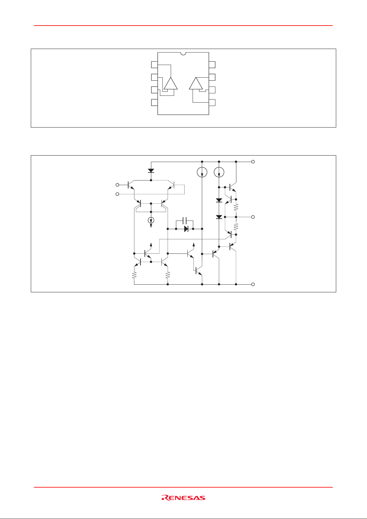
Circuit Schematic (1/2)
Vin(+)
−
Vin(
1
Vout1
V
EE
to V
to V
2
12
− ++−
3
4
(Top View)
EE
CC
to V
CC
Vin(−)1
Vin(+)1
)
8
7
6
5
V
CC
Vout2
Vin(−)2
Vin(+)2
V
CC
Vout
V
EE
Rev.1.00 Jun 15, 2005 page 2 of 8
Page 3
HA17458 Series
Absolute Maximum Ratings
(Ta = 25°C)
Ratings
Item Symbol
Supply voltage VCC +18 +18 +18 +18 V
V
Intput voltage V
Differential input voltage V
–18 –18 –18 –18 V
EE
3
±15 ±15 ±15 ±15 V
*
IN
±30 ±30 ±30 ±30 V
IN(diff)
Power dissipation PT 670*1 670*1 385*2 385*2 mW
Operating temperature Topr –20 to +75 –20 to +75 –20 to +75 –20 to +75 °C
Storage temperature Tstg –55 to +125 –55 to +125 –55 to +125 –55 to +125 °C
Notes: 1. These are the allowable values up to Ta = 45 °C. Derate by 8.3mW/°C above that temperature.
2. These are the allowable values up to Ta = 31 °C mounting on 30% wiring density glass epoxy board. Derate
by 7.14mW/°C above that temperature.
3. If the supply voltage is less than ±15V, input voltage should be less than supply voltage.
HA17458 HA17458PS HA17458F HA17458FP
Unit
Electrical Characteristics 1
(VCC = –VEE = 15V, Ta = 25°C)
Item Symbol Min Typ Max Unit Test conditions
Input offset voltage VIO — 2.0 6.0 mV RS ≤ 10kΩ
Input offset current IIO — 6 200 nA
Input bias current IIB — 30 500 nA
Line regulation ∆VIO/∆VCC — 30 150 µV/V RS ≤ 10kΩ
∆VIO/∆VEE — 30 150 µV/V RS ≤ 10kΩ
Voltage gain AVD 86 100 — dB RL ≥ 2kΩ, Vout = ±10V
Common mode rejection ratio CMR 70 90 — dB RS ≤ 10kΩ
Common mode input voltage range VCM ±12 ±13 — V
Peak-to-peak output voltage Vop-p ±12 ±14 — V RL = 10kΩ
Power dissipation Pd — 90 200 mW No load, 2 channel
Slew rate SR — 0.6 — V/µs AVD = 1
Input resistance Rin 0.3 1.0 — MΩ
Input capacitance Cin — 6.0 — pF
Output resistance Rout — 75 — Ω
Electrical Characteristics 2
(VCC = –VEE = 15V, Ta = –20 to +75°C)
Item Symbol Min Typ Max Unit Test conditions
Input offset voltage VIO — — 9.0 mV RS ≤ 10kΩ
Input offset current IIO — — 400 nA
Input bias current IIB — — 1100 nA
Voltage gain AVD 80 — — dB RL ≥ 2kΩ, Vout = ±10V
Peak-to-peak output voltage Vop-p ±10 ±13 — V RL = 2kΩ
Rev.1.00 Jun 15, 2005 page 3 of 8
Page 4

HA17458 Series
Characteristic Curves
Input Offset Voltage
vs. Ambient Temperature
5
4
(mV)
IO
VCC = + 15 V
= −15 V
V
EE
<
10 kΩ
R
=
S
3
2
1
Input Offset Voltage V
0
−20020406080
Ambient Temperature Ta (°C)
Input Offset Current
vs. Ambient Temperature
20
16
(nA)
IO
VCC = + 15 V
= −15 V
V
EE
12
8
100
vs. Ambient Temperature
80
(nA)
IB
60
40
20
Input Bias Current I
0
−20
020406080
Ambient Temperature Ta (°C)
vs. Ambient Temperature
200
100
Input Bias Current
VCC = + 15 V
V
Power Dissipation
VCC = + 15 V
V
EE
No Load
Both Amplifiers
= −15 V
EE
= −15 V
4
Input Offset Current I
0
−20
0 20406080
Ambient Temperature Ta (°C)
Power Dissipation Pd (mW)
0
−20
0 20406080
Ambient Temperature Ta (°C)
Rev.1.00 Jun 15, 2005 page 4 of 8
Page 5

HA17458 Series
120
110
(dB)
VD
100
90
Voltage Gain A
80
70
−
20
Ambient Temperature Ta (
200
150
Voltage Gain
vs. Ambient Temperature
VCC = + 15 V
V
= −15 V
EE
= 2 kΩ
R
L
0 20406080
°
C)
Power Dissipation
vs. Supply Voltage
Ta = 25°C
No Load
Both Amplifiers
Output Short Current
vs. Ambient Temperature
50
40
(mA)
OS
30
20
10
Output Short Current I
0
−20
0 20406080
Ambient Temperature Ta (
Maximum Output Voltage Swing
vs. Supply Voltage
20
(V)
OP-P
16
Source
Sink
VCC = + 15 V
= −15 V
V
EE
V
= 0 V
OP-P
°C)
Ta = 25°C
R
= 2 kΩ
L
100
50
Power Dissipation Pd (mW)
0
±3 ±6 ±9 ±12 ±15
Supply Voltage VCC, VEE (V)
±18
12
OP-P
+V
8
ÐV
OP-P
4
0
Maximum Output Voltage Swing V
±3 ±6 ±9 ±12 ±15 ±18
Supply Voltage VCC, VEE (V)
Rev.1.00 Jun 15, 2005 page 5 of 8
Page 6

HA17458 Series
Voltage Gain vs. Frequency
120
VCC = +15 V
100
80
(dB)
VD
60
40
Voltage Gain A
20
0
10 30 100 300 1 k 3 k 10 k 30 k 100 k 300 k 1M
Frequency (Hz)
Phase Angle vs. Frequency
VEE = −15 V
Ta = 25°C
RL = 2 kΩ
0
−40
−80
Phase Angle (deg)
−120
−160
100 300 1 k 3 k 10 k 30 k 100 k 300 k 1 M 3 M
Frequency (Hz)
VCC = +15 V
VEE = −15 V
Ta = 25°C
RL = 2 kΩ
Rev.1.00 Jun 15, 2005 page 6 of 8
Page 7

HA17458 Series
Maximum Output Voltage Swing
vs. Frequency
28
24
20
VCC = +15 V
V
= −15 V
EE
Ta = 25°C
R
= 10 kΩ
L
16
12
8
4
Maximum Output Voltage Swing Vop-p (V)
0
100 1k 10k 100k500 5k 50k 500k
Frequency f (Hz)
Voltage Follower Large
10
Signal Pulse Response
VCC = +15 V
V
EE
R
L
C
L
Output
Ta = 25°C
= −15 V
= 2 kΩ
= 100 pF
Maximum Output Voltage Swing
vs. Load Resistance
16
12
8
VCC = +15 V
VEE = −15 V
Ta = 25°C
4
0
−4
−8
Maximum Output Voltage Swing Vop-p (V)
−12
−16
200 1k 10k500 5k
Load Resistance RL (Ω)
0
Input
Input and Output Voltage (V)
−10
0 20406080
Time (µs)
Rev.1.00 Jun 15, 2005 page 7 of 8
Page 8

HA17458 Series
Package Dimensions
RENESAS CodeJEITA Package Code Previous Code
PRDP0008AF-AP-DIP8-6.3x9.6-2.54
85
DP-8B
D
E
MASS[Typ.]
0.51g
14
0.89
Z
e
b
3
Dimension in Millimeters
Reference
Symbol
e
1
A
LA
b
p
θ
c
e
1
1
D
E
A
0.5
A
1
0.38 0.48
b
p
b
3
0.20 0.25 0.35
c
0
°
θ
2.29 2.54 2.79
e
Z
2.54
L
7.62
MaxNomMin
10.6
9.6
7.4
6.3
5.06
0.58
1.3
15
°
1.27
PRSP0008DE-BP-SOP8-4.4x4.85-1.27
*1
D
58
Previous CodeJEITA Package Code RENESAS Code
FP-8DGV
MASS[Typ.]
0.1g
F
NOTE)
1. DIMENSIONS"*1 (Nom)"AND"*2"
DO NOT INCLUDE MOLD FLASH.
2. DIMENSION"*3"DOES NOT
INCLUDE TRIM OFFSET.
Index mark
1
Z
e
Rev.1.00 Jun 15, 2005 page 8 of 8
b
E
E
H
*2
4
*3
b
p
Mx
A
y
p
c
Terminal cross section
( Ni/Pd/Au plating )
L
1
1
A
L
Detail F
Dimension in Millimeters
Reference
Symbol
Min Nom Max
D
E
A
2
A
1
A
b
p
b
1
c
c
1
θ
H
E
e
θ
x
y
Z
L
L
1
4.85
5.25
4.4
0.00 0.1 0.20
0.35 0.4
0.15 0.20 0.25
0
°
0.42 0.60 0.85
1.27
1.05
2.03
0.45
6.756.35
6.5
0.12
0.15
0.75
8
°
Page 9

Sales Strategic Planning Div. Nippon Bldg., 2-6-2, Ohte-machi, Chiyoda-ku, Tokyo 100-0004, Japan
Keep safety first in your circuit designs!
1. Renesas Technology Corp. puts the maximum effort into making semiconductor products better and more reliable, but there is always the possibility that trouble
may occur with them. Trouble with semiconductors may lead to personal injury, fire or property damage.
Remember to give due consideration to safety when making your circuit designs, with appropriate measures such as (i) placement of substitutive, auxiliary circuits,
(ii) use of nonflammable material or (iii) prevention against any malfunction or mishap.
Notes regarding these materials
1. These materials are intended as a reference to assist our customers in the selection of the Renesas Technology Corp. product best suited to the customer's
application; they do not convey any license under any intellectual property rights, or any other rights, belonging to Renesas Technology Corp. or a third party.
2. Renesas Technology Corp. assumes no responsibility for any damage, or infringement of any third-party's rights, originating in the use of any product data,
diagrams, charts, programs, algorithms, or circuit application examples contained in these materials.
3. All information contained in these materials, including product data, diagrams, charts, programs and algorithms represents information on products at the time of
publication of these materials, and are subject to change by Renesas Technology Corp. without notice due to product improvements or other reasons. It is
therefore recommended that customers contact Renesas Technology Corp. or an authorized Renesas Technology Corp. product distributor for the latest product
information before purchasing a product listed herein.
The information described here may contain technical inaccuracies or typographical errors.
Renesas Technology Corp. assumes no responsibility for any damage, liability, or other loss rising from these inaccuracies or errors.
Please also pay attention to information published by Renesas Technology Corp. by various means, including the Renesas Technology Corp. Semiconductor
home page (http://www.renesas.com).
4. When using any or all of the information contained in these materials, including product data, diagrams, charts, programs, and algorithms, please be sure to
evaluate all information as a total system before making a final decision on the applicability of the information and products. Renesas Technology Corp. assumes
no responsibility for any damage, liability or other loss resulting from the information contained herein.
5. Renesas Technology Corp. semiconductors are not designed or manufactured for use in a device or system that is used under circumstances in which human life
is potentially at stake. Please contact Renesas Technology Corp. or an authorized Renesas Technology Corp. product distributor when considering the use of a
product contained herein for any specific purposes, such as apparatus or systems for transportation, vehicular, medical, aerospace, nuclear, or undersea repeater
use.
6. The prior written approval of Renesas Technology Corp. is necessary to reprint or reproduce in whole or in part these materials.
7. If these products or technologies are subject to the Japanese export control restrictions, they must be exported under a license from the Japanese government and
cannot be imported into a country other than the approved destination.
Any diversion or reexport contrary to the export control laws and regulations of Japan and/or the country of destination is prohibited.
8. Please contact Renesas Technology Corp. for further details on these materials or the products contained therein.
RENESAS SALES OFFICES
Refer to "http://www.renesas.com/en/network" for the latest and detailed information.
Renesas Technology America, Inc.
450 Holger Way, San Jose, CA 95134-1368, U.S.A
Tel: <1> (408) 382-7500, Fax: <1> (408) 382-7501
Renesas Technology Europe Limited
Dukes Meadow, Millboard Road, Bourne End, Buckinghamshire, SL8 5FH, U.K.
Tel: <44> (1628) 585-100, Fax: <44> (1628) 585-900
Renesas Technology Hong Kong Ltd.
7th Floor, North Tower, World Finance Centre, Harbour City, 1 Canton Road, Tsimshatsui, Kowloon, Hong Kong
Tel: <852> 2265-6688, Fax: <852> 2730-6071
Renesas Technology Taiwan Co., Ltd.
10th Floor, No.99, Fushing North Road, Taipei, Taiwan
Tel: <886> (2) 2715-2888, Fax: <886> (2) 2713-2999
Renesas Technology (Shanghai) Co., Ltd.
Unit2607 Ruijing Building, No.205 Maoming Road (S), Shanghai 200020, China
Tel: <86> (21) 6472-1001, Fax: <86> (21) 6415-2952
Renesas Technology Singapore Pte. Ltd.
1 Harbour Front Avenue, #06-10, Keppel Bay Tower, Singapore 098632
Tel: <65> 6213-0200, Fax: <65> 6278-8001
© 2005. Renesas Technology Corp., All rights reserved. Printed in Japan.
http://www.renesas.com
Colophon 2.0
 Loading...