

Page 1
HA13173AH
Multiple Voltage Regulator for Car Audio
REJ03F0227-0100
Rev.1.00
Jan 16, 2007
Description
The HA13173AH is a multiple voltage regulator for car audio system. This IC has 5.0 V output for a microcontroller,
3.3 V output for a Digital Signal Processor, 8.0 V output for CD driver, 8.4 V output for audio control, 8.4 V output for
illuminations, and high side switch output for external output.
The HA13173AH also has FREG that is possible to control external PNP transistor. It is adjustable output voltage by
changing an external resistor.
Functions
• Standby current is 100 µA max.
• The Vdd output for microcontroller has backup function, by independent power supply line.
• Low saturation output (PNP output) used for audio output.
• Output current limit circuit to avoid device destruction caused by shorted output, etc.
• High surge input protector against VB and VBUP.
• Built in a thermal shutdown circuit to prevent against the thermal destruction.
• The package is PRSS0015DA-C (SP-15TGV).
Rev.1.00 Jan 16, 2007 page 1 of 9
Page 2
HA13173AH
Pin Description
Pin
No. Pin Name Specification
1 GND Ground — — — —
2 FREG_B External transistor bias operation Available Available Off Off
3 FREG_F FREG feed back terminal Available Available Off Off
4 ILM OUT 8.4 V output for ILM/500 mA max Available Off Off Off
5 CTL4 FREG control terminal Available Available Not
6 CD OUT 8.0 V output for CD/1.3 A max Available Off Off Off
7 DSP OUT 3.3 V output for DSP/250 mA max Available Off Off Off
8 VB Battery — — — —
9 CTL3 ILM control terminal Available Not
10 AUDIO OUT 8.4 V output for AUDIO/500 mA max Available Off Off Off
11 CTL1 DSP, CD, AUDIO control terminal Available Not
12 EXT OUT High side output/600 mA max Available Off Off Off
13 CTL2 EXT control terminal Available Not
14 VDD OUT 5.0 V output for microcontroller On On On Off
15 VBUP Back up — — — —
Normal TSD ON VB = 24 V VB = 50 V
Protection
available
available
available
available
Not
available
Not
available
Not
available
Not
available
Not
available
Not
available
Not
available
Rev.1.00 Jan 16, 2007 page 2 of 9
Page 3
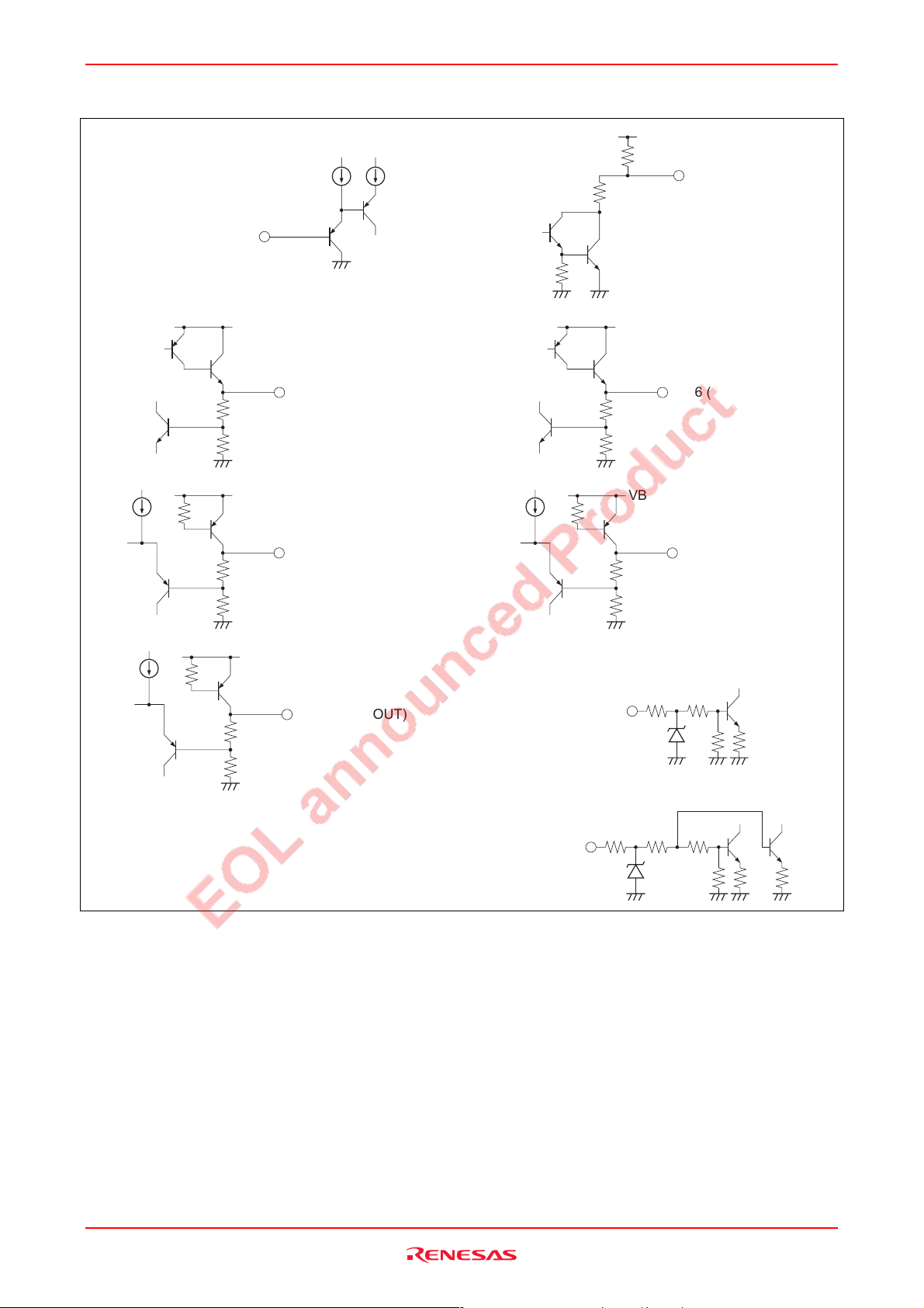
HA13173AH
Equivalent Circuit
Pin 3 (FREG_F)
VB
5 kΩ
Pin 2 (FREG_B)
100 Ω
VB
71 kΩ
13 kΩ
VB
71 kΩ
13 kΩ
VBUP
37 kΩ
15 kΩ
Pin 4 (ILMOUT)
Pin 10 (AUDIOOUT)
Pin 14 (VDDOUT)
10 kΩ
VB
Pin 6 (CDOUT)
67 kΩ
13 kΩ
VB
Pin 7 (DSPOUT)
20 kΩ
13 kΩ
10kΩ90
Pin 5 (CTL4)
Pin 9 (CTL43)
Pin 13 (CTL2)
kΩ
100
kΩ
30
kΩ
Rev.1.00 Jan 16, 2007 page 3 of 9
Pin 11 (CTL1)
10kΩ90kΩ90
kΩ
kΩ
75
30
kΩ
30
kΩ
Page 4

HA13173AH
A
Timing Chart
VB
VBUP
VDDOUT
CTL1
UDIOOUT
21 V
0 V
26 V
5.5 V
0 V
5 V
8.4 V
0 V
Load dump
τ = CBUP × 300 Ω
L
H
M
L
3.3 V
DSPOUT
0 V
8.0 V
CDOUT
0 V
0 V
8.4 V
0 V
Variable
0 V
Limiter
(IB)
0 A
VB
H
L
H
L
to maximum current, because impossible to sense
saturation of external Trs.
CTL2
EXTOUT
CTL3
ILMOUT
CTL4
FREG
(VOUT)
FREG_B
Rev.1.00 Jan 16, 2007 page 4 of 9
Page 5

HA13173AH
Block Diagram
CTL1
11
1.5 V
3.5 V
+
−
+B
DBUP
VB
8
+
−
Over voltage detect
BIAS
TSD
15
VBUP
+
CBUP
100 µF
CFREG
10 µF
DEXT1
DEXT2
QFREG
+
CTL2
CTL3
CTL4
EXT OUT
CEXT
10 µF
ILM OUT
CILM
0.1 µF
FREG_B
RFREG1
RFREG2
13
2.5 V
9
2.5 V
5
2.5 V
12
+
4
2
+
−
+
−
+
−
FREG_F
V
REF
−
+
−
+
−
+
V
REF
V
+
REF
−
−
+
3
GND
1
GND
+
−
−
+
TAB
VDD OUT
14
DSP OUT
7
CD OUT
6
AUDIO OUT
10
+
CVDD
10 µF
+
CDSP
10 µF
CCD
0.1 µF
+
CAUDIO
10 µF
Note: TAB (header of IC) connected to GND.
Rev.1.00 Jan 16, 2007 page 5 of 9
Page 6

HA13173AH
Absolute Maximum Ratings
(Ta = 25°C)
Item Symbol Rating Unit Note
Operating power supply voltage 1 Vcc1 19 V
Operating power supply voltage 2 Vcc2 24 V 1
Peak voltage Vcc(PEAK) 50 V 2
Power dissipation Pd 36 W 3
Junction temperature Tj 150 °C
Operating temperature Topr –40 to +85 °C
Storage temperature Tstg –55 to +125 °C
Notes: Recommended power supply voltage range 10 to 16 V.
1. Applied time is less than 60 s.
2. Surge pulse as input.
3. Ta = 25°C. : Permissible power dissipation when using a heat sink of infinite area. Refer to the derating
curves below.
20
15
thin = 1.6 mm, 100 cm Aluminum heat sink
11.0 W
10
8.7 W
5
Power dissipation Pd (W)
1.8 W
0
0501007525
thin = 1.6 mm, 50 cm Aluminum heat sink
w/o heat sink
Ambient temperature Ta (°C)
150125 175
Rev.1.00 Jan 16, 2007 page 6 of 9
Page 7

HA13173AH
Electrical Characteristics
Item Symbol Min Typ Max Unit Test Condition
Standby current IST — 65 100 µA CTL1, 2, 3, 4 = 0 V
CTL1 L level (DSP, AUDIO, CD OFF) VC1L 0.0 — 1.0 V
CTL1 M level (DSP, AUDIO ON, CD OFF) VC1M 2.0 — 3.0 V
CTL1 H level (DSP, AUDIO, CD ON) VC1H 4.0 — 6.0 V
CTL2 L level (EXT OFF) VC2L 0.0 — 2.0 V
CTL2 H level (EXT ON) VC2H 3.0 — 6.0 V
CTL3 L level (ILM OFF) VC3L 0.0 — 2.0 V
CTL3 H level (ILM ON) VC3H 3.0 — 6. 0 V
CTL4 L level (FREG OFF) VC4L 0.0 — 2.0 V
CTL4 H level (FREG ON) VC4H 3.0 — 6. 0 V
VDD
OUT
CD
OUT
AUDIO
OUT
DSP
OUT
ILM
OUT
EXT
OUT
FREG
OUT
Output voltage Vo1 4.75 5.00 5.25 V Io1 = 160 mA
Voltage regulation ∆Vo11 — 10 50 mV Vcc = 10 to 16 V, Io1 = 160 mA
Load regulation ∆Vo12 — 50 100 mV Io1 = 0 to 160 mA
Minimum I/O voltage
differential
Output current capacity Io1 200 400 — mA Vo1 ≥ 4.7 V
Ripple rejection ratio SVR1 45 55 — dB f = 100 Hz, Io1 = 160 mA
Output voltage Vo2 7.6 8.0 8.4 V Io2 = 1.0 A
Voltage regulation ∆Vo21 — 40 100 mV Vcc = 10 to 16V, Io2 = 1.0 A
Load regulation ∆Vo22 — 70 150 mV Io2 = 10m to 1.0 A
Minimum I/O voltage
differential
Output current capacity Io2 1.3 2.0 — mA Vo2 ≥ 7.6 V
Ripple rejection ratio SVR2 40 50 — dB f = 100 Hz, Io2 = 1.0 A
Output voltage Vo3 8.1 8.4 8.7 V Io3 = 400 mA
Voltage regulation ∆Vo31 — 30 90 mV Vcc = 10 to 16 V, Io3 = 400 mA
Load regulation ∆Vo32 — 100 200 mV Io3 = 10 to 400 mA
Minimum I/O voltage
differential
Output current capacity Io3 500 850 — mA Vo3 ≥ 8.1 V
Ripple rejection ratio SVR3 45 50 — dB f = 100 Hz, Io3 = 400 mA
Output voltage Vo4 3.1 3.3 3.5 V Io4 = 200 mA
Voltage regulation ∆Vo41 — 40 100 mV Vcc = 10 to 16 V, Io4 = 200 mA
Load regulation ∆Vo42 — 50 100 mV Io4 = 0 to 200 mA
Output current capacity Io4 250 500 — mA Vo4 ≥ 3.1 V
Ripple rejection ratio SVR4 45 55 — dB f = 100 Hz, Io4 = 200 mA
Output voltage Vo5 8.0 8.4 8.8 V Io5 = 400 mA
Voltage regulation ∆Vo51 — 40 100 mV Vcc = 10 to 16 V, Io5 = 400 mA
Load regulation ∆Vo52 — 70 150 mV Io5 = 10 to 400 mA
Minimum I/O voltage
differential
Output current capacity Io5 500 900 — mA Vo5 ≥ 8.0 V
Ripple rejection ratio SVR5 40 50 — dB f = 100 Hz, Io5 = 400 mA
Minimum I/O voltage
differential
Load regulation ∆Vo62 — 200 400 mV Io6 = 10 to 480 mA
Output current capacity Io6 600 900 — mA Vo61 ≤ 1.0 V
FREG_F Output voltage V FF7 1.17 1.23 1.29 V Iload (external PNP) = 400 mA
FREG_F Voltage regulation ∆VFF71 — 10 25 mV Vcc = 10 to 16 V, Iload = 400 mA
FREG_F Load regulation ∆VFF72 — 10 25 mV Iload = 10 to 400 mA
FREG_B Output current
capacity
FREG_F input bias current IFF7 — 50 300 nA
∆Vo13 — 0.4 0.9 V Io1 = 160 mA
∆Vo23 — 1.0 1.5 V Io2 = 1.0 A
∆Vo33 — 0.4 0.9 V Io3 = 400 mA
∆Vo53 — 1.0 1.3 V Io5 = 400 mA
∆Vo61 — 0.6 1.0 V Vcc = 10 to 16 V, Io6 = 480 mA
IFB7 30 30 — mA VFF ≥ 1.17 V
Rev.1.00 Jan 16, 2007 page 7 of 9
Page 8

HA13173AH
Evaluation Circuit
HA13173AH
CFREG2
1 µF
CFREG1
GND
10 µF
FREG_B FREG_F
1
+
RFREG1
RFREG2
2 3
QFREG
2SB857
FREG
ILM
OUT5CTL4
4
CILM
0.1
µF
CTL4ILM
CD
DSP
OUT
OUT8VB9CTL3
6
7
CCD
0.1
µF
CD
DSP
CDSP
+
10
µF
C1
100 µF
+B
AUDIO
OUT11CTL1
10
CAUDIO
+
10
µF
AUDIO
+
C2
0.1 µF
CTL1CTL3
EXT
OUT13CTL2
12
CEXT
+
10
µF
EXT
CTL2
VDD
OUT15VBUP
14
CVDD
+
10
µF
VDD
CBUP
100 µF
+
Rev.1.00 Jan 16, 2007 page 8 of 9
Page 9

HA13173AH
Package Dimensions
P-HSIP15-14.3x19.66-1.27 3.0g
SP-15TGVPRSS0015DA-C
RENESAS CodeJEITA Package Code Previous Code
MASS[Typ.]
20.5 MAX
19.66
±
0.3
19.0
0.2
±
3.0
0.3
±
±
0.2
3.6
φ
11.3
±
1.11
0.25
±
0.1
0.6
1.27
2.54
Unit : mm
0.25
1.8
3.5
6.04
3.53.3MiN TYP 3.8MAX
1.281.1MiN TYP 1.50MAX
13.8
+0.10
-0.05
±
0.25
*1
±
0.5
*1
±
0.5
17.9
±
0.2
2-C3.0
7.8
*1
±
0.25
*1
±
0.25
Note) 1. Dimension "*1" is the value after bending.
( Ni/Pd/Au plating )
Rev.1.00 Jan 16, 2007 page 9 of 9
Page 10

Sales Strategic Planning Div. Nippon Bldg., 2-6-2, Ohte-machi, Chiyoda-ku, Tokyo 100-0004, Japan
Notes:
1. This document is provided for reference purposes only so that Renesas customers may select the appropriate Renesas products for their use. Renesas neither makes
warranties or representations with respect to the accuracy or completeness of the information contained in this document nor grants any license to any intellectual property
rights or any other rights of Renesas or any third party with respect to the information in this document.
2. Renesas shall have no liability for damages or infringement of any intellectual property or other rights arising out of the use of any information in this document, including,
but not limited to, product data, diagrams, charts, programs, algorithms, and application circuit examples.
3. You should not use the products or the technology described in this document for the purpose of military applications such as the development of weapons of mass
destruction or for the purpose of any other military use. When exporting the products or technology described herein, you should follow the applicable export control laws
and regulations, and procedures required by such laws and regulations.
4. All information included in this document such as product data, diagrams, charts, programs, algorithms, and application circuit examples, is current as of the date this
document is issued. Such information, however, is subject to change without any prior notice. Before purchasing or using any Renesas products listed in this document,
please confirm the latest product information with a Renesas sales office. Also, please pay regular and careful attention to additional and different information to be
disclosed by Renesas such as that disclosed through our website. (http://www.renesas.com )
5. Renesas has used reasonable care in compiling the information included in this document, but Renesas assumes no liability whatsoever for any damages incurred as a
result of errors or omissions in the information included in this document.
6. When using or otherwise relying on the information in this document, you should evaluate the information in light of the total system before deciding about the applicability
of such information to the intended application. Renesas makes no representations, warranties or guaranties regarding the suitability of its products for any particular
application and specifically disclaims any liability arising out of the application and use of the information in this document or Renesas products.
7. With the exception of products specified by Renesas as suitable for automobile applications, Renesas products are not designed, manufactured or tested for applications
or otherwise in systems the failure or malfunction of which may cause a direct threat to human life or create a risk of human injury or which require especially high quality
and reliability such as safety systems, or equipment or systems for transportation and traffic, healthcare, combustion control, aerospace and aeronautics, nuclear power, or
undersea communication transmission. If you are considering the use of our products for such purposes, please contact a Renesas sales office beforehand. Renesas shall
have no liability for damages arising out of the uses set forth above.
8. Notwithstanding the preceding paragraph, you should not use Renesas products for the purposes listed below:
(1) artificial life support devices or systems
(2) surgical implantations
(3) healthcare intervention (e.g., excision, administration of medication, etc.)
(4) any other purposes that pose a direct threat to human life
Renesas shall have no liability for damages arising out of the uses set forth in the above and purchasers who elect to use Renesas products in any of the foregoing
applications shall indemnify and hold harmless Renesas Technology Corp., its affiliated companies and their officers, directors, and employees against any and all
damages arising out of such applications.
9. You should use the products described herein within the range specified by Renesas, especially with respect to the maximum rating, operating supply voltage range,
movement power voltage range, heat radiation characteristics, installation and other product characteristics. Renesas shall have no liability for malfunctions or damages
arising out of the use of Renesas products beyond such specified ranges.
10. Although Renesas endeavors to improve the quality and reliability of its products, IC products have specific characteristics such as the occurrence of failure at a certain
rate and malfunctions under certain use conditions. Please be sure to implement safety measures to guard against the possibility of physical injury, and injury or damage
caused by fire in the event of the failure of a Renesas product, such as safety design for hardware and software including but not limited to redundancy, fire control and
malfunction prevention, appropriate treatment for aging degradation or any other applicable measures. Among others, since the evaluation of microcomputer software
alone is very difficult, please evaluate the safety of the final products or system manufactured by you.
11. In case Renesas products listed in this document are detached from the products to which the Renesas products are attached or affixed, the risk of accident such as
swallowing by infants and small children is very high. You should implement safety measures so that Renesas products may not be easily detached from your products.
Renesas shall have no liability for damages arising out of such detachment.
12. This document may not be reproduced or duplicated, in any form, in whole or in part, without prior written approval from Renesas.
13. Please contact a Renesas sales office if you have any questions regarding the information contained in this document, Renesas semiconductor products, or if you have
any other inquiries.
RENESAS SALES OFFICES
http://www.renesas.com
Refer to "http://www.renesas.com/en/network" for the latest and detailed information.
Renesas Technology America, Inc.
450 Holger Way, San Jose, CA 95134-1368, U.S.A
Tel: <1> (408) 382-7500, Fax: <1> (408) 382-7501
Renesas Technology Europe Limited
Dukes Meadow, Millboard Road, Bourne End, Buckinghamshire, SL8 5FH, U.K.
Tel: <44> (1628) 585-100, Fax: <44> (1628) 585-900
Renesas Technology (Shanghai) Co., Ltd.
Unit 204, 205, AZIACenter, No.1233 Lujiazui Ring Rd, Pudong District, Shanghai, China 200120
Tel: <86> (21) 5877-1818, Fax: <86> (21) 6887-7898
Renesas Technology Hong Kong Ltd.
7th Floor, North Tower, World Finance Centre, Harbour City, 1 Canton Road, Tsimshatsui, Kowloon, Hong Kong
Tel: <852> 2265-6688, Fax: <852> 2730-6071
Renesas Technology Taiwan Co., Ltd.
10th Floor, No.99, Fushing North Road, Taipei, Taiwan
Tel: <886> (2) 2715-2888, Fax: <886> (2) 2713-2999
Renesas Technology Singapore Pte. Ltd.
1 Harbour Front Avenue, #06-10, Keppel Bay Tower, Singapore 098632
Tel: <65> 6213-0200, Fax: <65> 6278-8001
Renesas Technology Korea Co., Ltd.
Kukje Center Bldg. 18th Fl., 191, 2-ka, Hangang-ro, Yongsan-ku, Seoul 140-702, Korea
Tel: <82> (2) 796-3115, Fax: <82> (2) 796-2145
Renesas Technology Malaysia Sdn. Bhd
Unit 906, Block B, Menara Amcorp, Amcorp Trade Centre, No.18, Jalan Persiaran Barat, 46050 Petaling Jaya, Selangor Darul Ehsan, Malaysia
Tel: <603> 7955-9390, Fax: <603> 7955-9510
© 2007. Renesas Technology Corp., All rights reserved. Printed in Japan.
Colophon .7.0
 Loading...