

Page 1
REJ10B0200-0200
H8SX/1653 Group E6000H TFP-120
User System Interface Board
HS1653ECN61H User’s Manual
Renesas Microcomputer Development Environment System
HS1653ECN61HE
Rev.2.00
Revision Date: Dec. 09, 2005
Page 2

Page 3
Keep safety first in your circuit designs!
1. Renesas Technology Corp. puts the maximum effort into making semiconductor products better and
more reliable, but there is always the possibility that trouble may occur with them. Trouble with
semiconductors may lead to personal injury, fire or property damage.
Remember to give due consideration to safety when making your circuit designs, with appropriate
measures such as (i) placement of substitutive, auxiliary circuits, (ii) use of nonflammable material or
(iii) prevention against any malfunction or mishap.
Notes regarding these materials
1. These materials are intended as a reference to assist our customers in the selection of the Renesas
Technology Corp. product best suited to the customer's application; they do not convey any license
under any intellectual property rights, or any other rights, belonging to Renesas Technology Corp. or
a third party.
2. Renesas Technology Corp. assumes no responsibility for any damage, or infringement of any thirdparty's rights, originating in the use of any product data, diagrams, charts, programs, algorithms, or
circuit application examples contained in these materials.
3. All information contained in these materials, including product data, diagrams, charts, programs and
algorithms represents information on products at the time of publication of these materials, and are
subject to change by Renesas Technology Corp. without notice due to product improvements or
other reasons. It is therefore recommended that customers contact Renesas Technology Corp. or
an authorized Renesas Technology Corp. product distributor for the latest product information
before purchasing a product listed herein.
The information described here may contain technical inaccuracies or typographical errors.
Renesas Technology Corp. assumes no responsibility for any damage, liability, or other loss rising
from these inaccuracies or errors.
Please also pay attention to information published by Renesas Technology Corp. by various means,
including the Renesas Technology Corp. Semiconductor home page (http://www.renesas.com).
4. When using any or all of the information contained in these materials, including product data,
diagrams, charts, programs, and algorithms, please be sure to evaluate all information as a total
system before making a final decision on the applicability of the information and products. Renesas
Technology Corp. assumes no responsibility for any damage, liability or other loss resulting from the
information contained herein.
5. Renesas Technology Corp. semiconductors are not designed or manufactured for use in a device or
system that is used under circumstances in which human life is potentially at stake. Please contact
Renesas Technology Corp. or an authorized Renesas Technology Corp. product distributor when
considering the use of a product contained herein for any specific purposes, such as apparatus or
systems for transportation, vehicular, medical, aerospace, nuclear, or undersea repeater use.
6. The prior written approval of Renesas Technology Corp. is necessary to reprint or reproduce in
whole or in part these materials.
7. If these products or technologies are subject to the Japanese export control restrictions, they must
be exported under a license from the Japanese government and cannot be imported into a country
other than the approved destination.
Any diversion or reexport contrary to the export control laws and regulations of Japan and/or the
country of destination is prohibited.
8. Please contact Renesas Technology Corp. for further details on these materials or the products
contained therein.
Page 4

Page 5

IMPORTANT INFORMATION
READ FIRST
• READ this user's manual before using this user system interface board.
• KEEP the user's manual handy for future reference.
Do not attempt to use the user system interface board until you fully understand its
mechanism.
User System Interface Board:
Throughout this document, the term "user system interface board" shall be defined as the
following product produced only by Renesas Technology Corp. excluding all subsidiary products.
• User system interface board (HS1653ECN61H)
The user system or a host computer is not included in this definition.
Purpose of the User System Interface Board:
This user system interface board is for connecting the evaluation chip board and user system.
This user system interface board must only be used for the above purpose.
Improvement Policy:
Renesas Technology Corp. (including its subsidiaries, hereafter collectively referred to as
Renesas) pursues a policy of continuing improvement in design, performance, functions, and
safety of the user system interface board. Renesas reserves the right to change, wholly or
partially, the specifications, design, user's manual, and other documentation at any time without
notice.
Target User of the User System Interface Board:
This user system interface board should only be used by those who have carefully read and
thoroughly understood the information and restrictions contained in the user's manual. Do not
attempt to use the user system interface board until you fully understand its mechanism.
It is highly recommended that first-time users be instructed by users that are well versed in the
operation of the user system interface board.
I
Page 6
LIMITED WARRANTY
Renesas warrants its user system interface boards to be manufactured
in accordance with published specifications and free from defects in
material and/or workmanship. Renesas will repair or replace any
user system interface boards determined to be defective in material
and/or workmanship. User system interface boards are wearing parts
which Renesas will not repair or replace if damaged and/or worn
through use. The foregoing shall constitute the sole remedy for any
breach of Renesas’ warranty. This warranty extends only to you, the
original Purchaser. It is not transferable to anyone who subsequently
purchases the user system interface board from you. Renesas is not
liable for any claim made by a third party or made by you for a third
party.
DISCLAIMER
RENESAS MAKES NO WARRANTIES, EITHER EXPRESS OR
IMPLIED, ORAL OR WRITTEN, EXCEPT AS PROVIDED
HEREIN, INCLUDING WITHOUT LIMITATION THEREOF,
WARRANTIES AS TO MARKETABILITY, MERCHANTABILITY,
FITNESS FOR ANY PARTICULAR PURPOSE OR USE, OR
AGAINST INFRINGEMENT OF ANY PATENT. IN NO EVENT
SHALL RENESAS BE LIABLE FOR ANY DIRECT, INCIDENTAL
OR CONSEQUENTIAL DAMAGES OF ANY NATURE, OR
LOSSES OR EXPENSES RESULTING FROM ANY DEFECTIVE
USER SYSTEM INTERFACE BOARD, THE USE OF ANY USER
SYSTEM INTERFACE BOARD, OR ITS DOCUMENTATION,
EVEN IF ADVISED OF THE POSSIBILITY OF SUCH DAMAGES.
EXCEPT AS EXPRESSLY STATED OTHERWISE IN THIS
WARRANTY, THIS USER SYSTEM INTERFACE BOARD IS SOLD
"AS IS ", AND YOU MUST ASSUME ALL RISK FOR THE USE
AND RESULTS OBTAINED FROM THE USER SYSTEM
INTERFACE BOARD.
II
Page 7

State Law:
Some states do not allow the exclusion or limitation of implied warranties or liability for
incidental or consequential damages, so the above limitation or exclusio n may not apply to you.
This warrant y gi ves yo u spec i fic le gal rig hts, and you ma y ha ve ot her rig hts which may vary fro m
state to state.
The Warranty is Void in the Following Cases:
Renesas shall have no liability or legal responsibility for any problems caused by misuse,
abuse, misapplication, neglect, improper handling, installation, repair or modifications of the user
system interface board without Renesas’ prior written consent or any problems caused by the user
system.
All Rights Reserved:
This user's manual and user system interface board are copyrighted and all rights are reserved
by Renesas. No part of this user's manual, all or part, may be reproduced or duplicated in any
form, in hard-copy or machine-readable form, by any means available without Renesas’ prior
written consent.
Other Important Things to Keep in Mind:
1. Circuitry and other examples described herein are meant merely to indicate the characteristics
and perfor mance of Renesas’ semiconductor products. Renesas assumes no responsibility for
any intellectual property claims or other problems that may result from applications based on
the examples described herein.
2. No license is granted by implication or otherwise under any patents or other rights of any third
party or Renesas.
Figures:
Some figures i n this user's manual may s how items diffe rent from your actual system.
Limited Anticipation of Danger:
Renesas cannot anticipate every possible circumstance that might involve a potential hazard.
The warnings in this user's manual and on the user system interface board are therefore not all
inclusive. Therefore, you must use the user system interface board safely at your own risk.
III
Page 8

SAFETY PAGE
READ FIRST
• READ this user's manual before using this user system interface board.
• KEEP the user's manual handy for future reference.
Do not attempt to use the user system interface board until you fully understand its
mechanism.
DEFINITION OF SIGNAL WORDS
This is the safety alert symbol. It is used to alert you to potential personal
injury hazards. Obey all safety messages that follow this symbol to avoid
possible injury or death.
DANGER
avoided, will result in death or serious injury.
WARNING
avoided, could result in death or serious injury.
CAUTION
avoided, may result in minor or moderate injury.
CAUTION
potentially hazardous situation which, if not avoided, may result
in property damage.
DANGER indicates an imminently hazardous situatio n whic h, if not
WARNING indicates a potentially hazardous situation which, if not
CAUTION indic a tes a potentia lly hazar do us situat io n which, if not
CAUTION used without the safety alert symbol indicates a
NOTE
IV
emphasizes essential information.
Page 9
WARNING
Observe the precautions listed below. Failure to do so
will result in a FIRE HAZARD and will damage the user
system and the emulator product or will result in
PERSONAL INJURY. The USER PROGRAM will be
LOST.
1. Do not repair or remodel the emulator product by
yourself for electric shock prevention and quality
assurance.
2. Always switch OFF the E6000H emulator and user system
before connecting or disconnecting any CABLES or
PARTS.
3. Always before connecting any BOARDS, make sure that
pin 1 on both sides are correctly aligned.
V
Page 10

Preface
The HS1653ECN61H is a user system interface board that connects a user system for the
H8SX/1653 TFP-120 package to the H8SX/1650 E6000H emulator (HS1650EPH60H).
Emulation of the H8SX/1653 group is only possible when this user system interface board is
connected to the HS1650EPH60H.
i
Page 11

Contents
Section 1 Configuration.....................................................................................1
Section 2 Connection Procedures......................................................................3
2.1 Connecting User System Interface Board to User System................................................3
2.1.1 Installing IC Socket..............................................................................................4
2.1.2 Soldering IC Socket.............................................................................................4
2.1.3 Installing IC Socket..............................................................................................4
2.1.4 Fastening IC Socket Connector............................................................................5
2.2 Exchanging the Spacer of the Evaluation Chip Board......................................................7
2.3 Connecting User System Interface Board to Evaluation Chip Board...............................8
2.4 Recommended Dimensions for User System Mount Pad (Footprint)...............................10
2.5 Dimensions for Evaluation Chip Board and User System Interface Board......................11
2.6 Resulting Dimensions after Connecting User System Interface Board.............................12
2.7 Using the Emulator without Connecting User System......................................................13
Section 3 User System Interface Circuits..........................................................15
Section 4 Verifying Operation...........................................................................18
Section 5 Notice.................................................................................................20
Section 6 Restrictions........................................................................................22
ii
Page 12

Section 1 Configuration
Figure 1 and table 1 show the configuration and components of the user system interface board for
the TFP-120 package. Please make sure you have all of these components when unpacking.
Evaluation chip board
Screws (M2 × 8 mm)
with flat washers
Socket cover
Figure 1 User System Interface Board for the H8SX/1653 TFP-120 Package
Spacer
User system
Screws (M2 × 12 mm)
with flat washers
(for fastening cable head)
User system
interface board
IC socket
1
Page 13

CAUTION
Use an IC149-120-043-B51 socket (manufactured by
YAMAICHI ELECTRONICS Co., Ltd.) for the TFP-120 package
IC socket on the user system.
Table 1 HS1653ECN61H Components
No. Component Quantity Remarks
1 User system interface
board
2 IC socket 1 For the TFP-120 package (to be mounted on the user
3 Socket cover 1 For installing a TFP-120-packaged MCU
4 Screw (M2 x 12 mm) 4 For fastening cable head (with four flat washers)
5 Screw (M2 x 8 mm) 4 For installing a TFP-120-packaged MCU (with four flat
6 Spacers (2.6MP x 25 mm) 2
7 Spacers (2.6MQ x 16 mm) 4
8 User’s manual 1 User’s manual for HS1653ECN61H (this manual)
1
system)
washers)
2
Page 14

Section 2 Connection Procedures
2.1 Connecting User System Interface Board to User System
WARNING
Always switch OFF the user system and the emulator
product before the USER SYSTEM INTERFACE BOARD
is connected to or removed from any part. Before
connecting, make sure that pin 1 on both sides are correctly
aligned. Failure to do so will result in a FIRE HAZARD and
will damage the user system and the emulator product or
will result in PERSONAL INJURY. The USER PROGRAM will
be LOST.
CAUTION
1. Do not connect a 5-V signal to any pin, including the
USB pins. Incorrect usage will cause damage to the
emulator product, user system interface board, and
user system.
2. To connect the emulator to the user system, ensure that
the SW1 jumper pin is inserted to [ON].
Failure to do so will damage the emulator product, user
system interface board, and user system.
3
Page 15

To connect the cable head to the user system, follow the instructions below.
2.1.1 Installing IC Socket
After checking the location of pin 1 on the IC socket, apply epoxy resin adhesive to the bottom of
the IC socket for a TFP-120 package, and fasten it to the user system before soldering.
2.1.2 Soldering IC Socket
After fastening, solder the IC socket for a TFP-120 package to the user system. Be sure to
completely solder the leads so that the solder slops gently over the leads and forms solder fillets.
(Use slightly more solder than the MCU.)
2.1.3 Installing IC Socket
CAUTION
Check the location of pin 1 before inserting.
After checking the location of pin 1 on the user system interface board and pin 1 on the IC socket
connector, align the guide pins on the IC socket connector with the guide holes on the user system
interface board, and insert the IC socket connector into the IC socket (figure 2).
4
Page 16

2.1.4 Fastening IC Socket Connector
CAUTION
1. Use the screwdriver provided for tightening screws.
2. The tightening torque must be 0.294 N•m or less.
If the applied torque cannot be accurately measured,
stop tightening when the force required to turn the screw
becomes significantly greater than that needed when first
tightening. If a screw is tightened too much, the screw
head may break or an IC socket contact error may be
caused by a crack in the IC socket solder.
3. If the emulator does not operate correctly, cracks might
have occurred in the solder. Check conduction with
a tester and re-solder the IC socket if necessary.
Fasten the user system interface board to the IC socket on the user system with four screws
(M2 × 12 mm) provided.
Take special care, such as manually securing the IC socket soldered area, to prevent the soldered
IC socket from being damaged by twisting the components.
5
Page 17

Screws (M2 × 12 mm)
with flat washers
(for fastening cable head)
User system interface board
Pin 1
IC socket
(IC149-120-043-B51
User system
manufactured by
YAMAICHI ELECTRONICS Co., Ltd.)
Figure 2 Connecting User System Interface Board to User System
6
Page 18
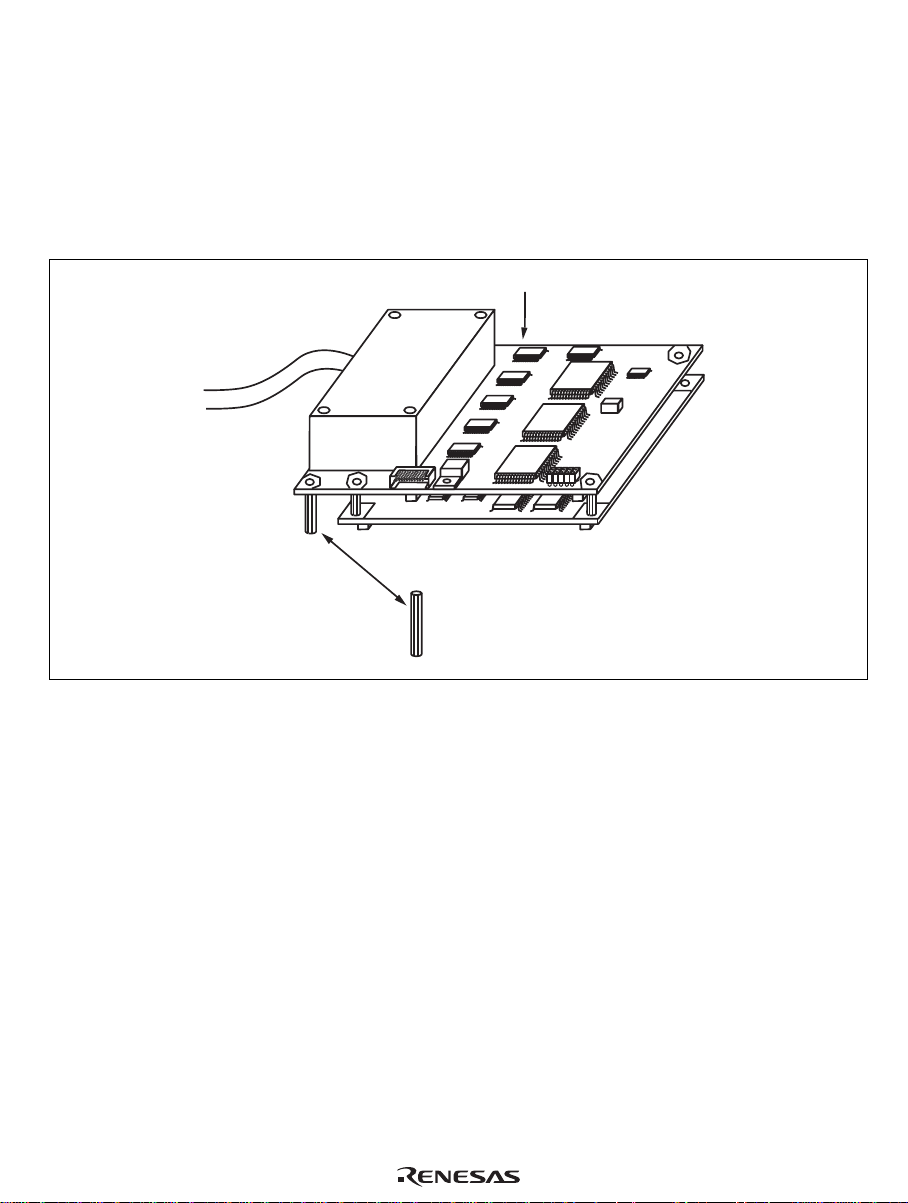
2.2 Exchanging the Spacer of the Evaluation Chip Board
While the user system interface board is connected to the user system, be careful not to apply
load.
Exchange the spacer (2.6MP × 10 mm) of the evaluation chip board with another spacer (2.6MP ×
25 mm) provided for the user system interface board.
Evaluation chip board
Spacer
(2.6MP × 25 mm)
Figure 3 Exchanging the Spacer
7
Page 19

2.3 Connecting User System Interface Board to Evaluation Chip Board
WARNING
Observe the precautions listed below. Failure to do so
will result in a FIRE HAZARD and will damage the user
system and the emulator product or will result in
PERSONAL INJURY. The USER PROGRAM will be
LOST.
1. Always switch OFF the user system and the emulator
product before the USER SYSTEM INTERFACE BOARD
is connected to or removed from any part. Before
connecting, make sure that pin 1 on both sides are
correctly aligned.
2. The user system interface board dedicated to the
emulator must be used.
1. Make sure that power of the user system and the emulator is turned off.
2. Align the connectors on the board with those on the evaluation chip board according to their
numbers (figure 4).
3. Adjust the height of the spacer of the evaluation chip board with the user system.
8
Page 20

Evaluation chip board
Connector No.
Evaluation
Chip Board
Connector No.
UCN1 UCN1
UCN2 UCN2
User system interface board
Board
Connector No.
Figure 4 Connecting User System Interface Board to Evaluation Chip Board
9
Page 21

2.4 Recommended Dimensions for User System Mount Pad (Footprint)
Figure 5 shows the recommended dimensions for the mount pad (footprint) for the user system
with an IC socket for a TFP-120 package (IC149-120-043-B51: manufactured by YAMAICHI
ELECTRONICS Co., Ltd). Note that the dimensions in figure 5 are somewhat different from
those of the actual chip's mount pad.
17.10 (min.)
13.80 (max.)
0.40 × 29 = 11.60 ± 0.05
0.40 ± 0.05 0.25 ± 0.05
0.40 ± 0.05
10
Unit: mm
Figure 5 Recommended Dimensions for Mount Pad
0.40 × 29 = 11.60 ± 0.05
Page 22

2.5 Dimensions for Evaluation Chip Board and User System Interface Board
The dimensions for the evaluation chip board and the user system interface board are shown in
figure 6.
140.0
100.0
Evaluation chip board
118.5
102.5 16.0
84.5
69.0
34.5
78.5
User system interface board
Unit: mm
Tolerance:
±
0.5 mm
Figure 6 Dimensions for Evaluation Chip Board and User System Interface Board
11
Page 23

2.6 Resulting Dimensions after Connecting User System Interface Board
The resulting dimensions, after connecting the user system interface board to the user system, are
shown in figure 7.
Evaluation chip board
57.6
35.6
16.0
56
Spacer (φ5.8)
.5
User system
56.5
IC socket
(IC149-120-043-B51
manufactured by
YAMAICHI ELECTRONICS Co., Ltd.)
45.0
45.0
Unit: mm
Tolerance: ±1.0 mm
Figure 7 Resulting Dimensions after Connecting User System Interface Board
12
Page 24

2.7 Using the Emulator without Connecting User System
WARNING
Always switch OFF the user system and the emulator
product before the USER SYSTEM INTERFACE BOARD
is connected to or removed from any part. Before
connecting, make sure that pin 1 on both sides are correctly
aligned. Failure to do so will result in a FIRE HAZARD and
will damage the user system and the emulator product or
will result in PERSONAL INJURY. The USER PROGRAM will
be LOST.
CAUTION
When this emulator is used without connecting to the
user system, ensure that the SW1 jumper pin is inserted to
[OFF]. Failure to do so will damage the emulator
product, user system interface cable, and user system.
Attach the provided spacers (2.6MQ x 16 mm) to fo ur positions on the user system interface board
not to apply loads to the connector (CN1) on the board.
13
Page 25

OFF
SW1
ON
USER
P1
Figure 8 SW1 Jumper Socket
14
Figure 9 Attaching Spacers
Spacer
(2.6MQ x 16 mm)
Page 26
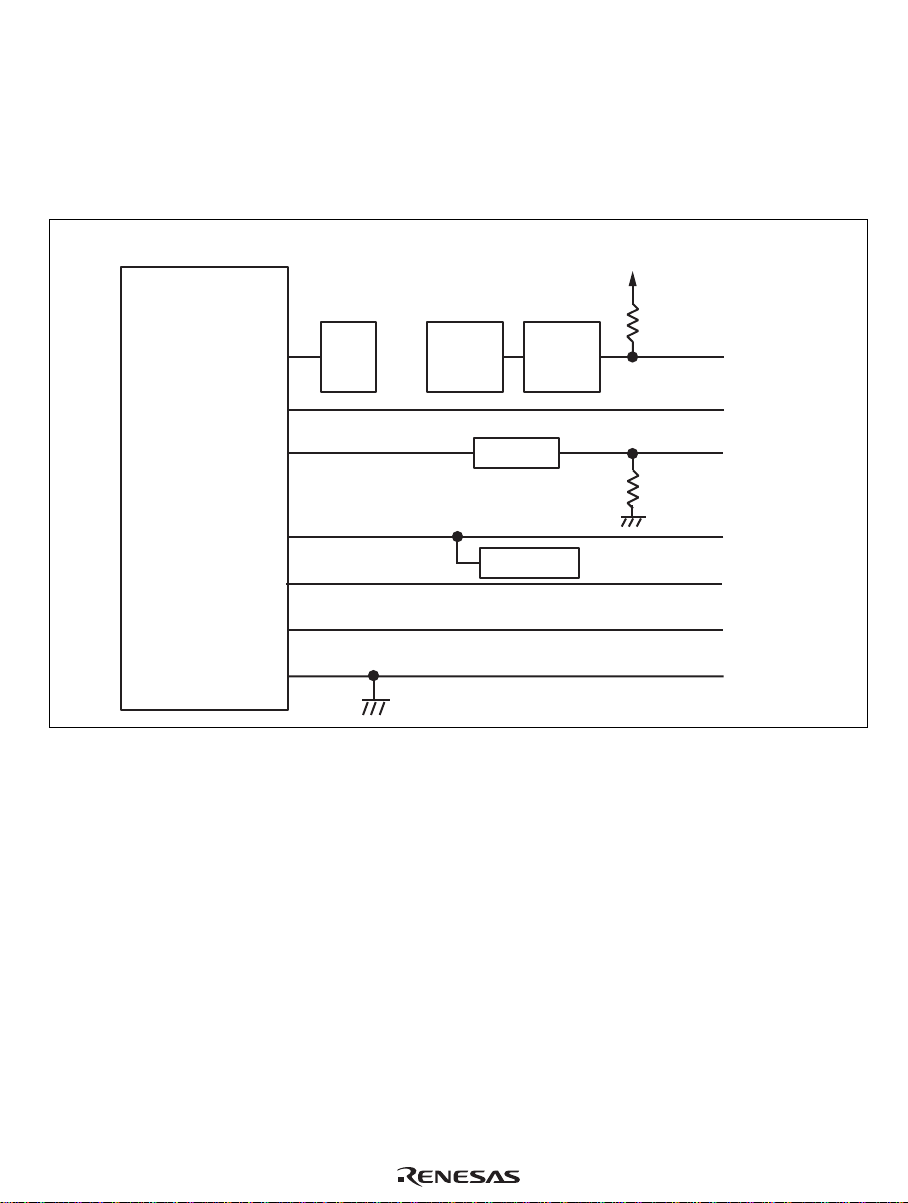
Section 3 User System Interface Circuits
The following user interface circuits are required for the emulator when the user system interface
board is in use.
Sub-MCU
MD_CLK
PM0-PM4
Vcc
MD control
circuit
VBUS
DrVcc DrVcc
USD-
USD+
DrVss
Monitoring
circuit
LPT16244
EPM7128
Power-supply
circuit
47 kΩ
1 kΩ
User system
MD_CLK
PM0-PM4
VBUS
USD-
USD+
DrVss
Figure 10 User System Interface Circuit (1)
Note: The power-supply circuit shown above is turned on/off by the setting of the SW1 jumper
pin on HS1653ECN61H. Ensure that the jumper pin is inserted to [ON] on
HS1653ECN61H when connecting the emulator (with HS1653ECN61H attached) to the
user system or supplying power to DrVCC. Otherwise the emulator product, user system
interface board, and user system will be damaged.
15
Page 27
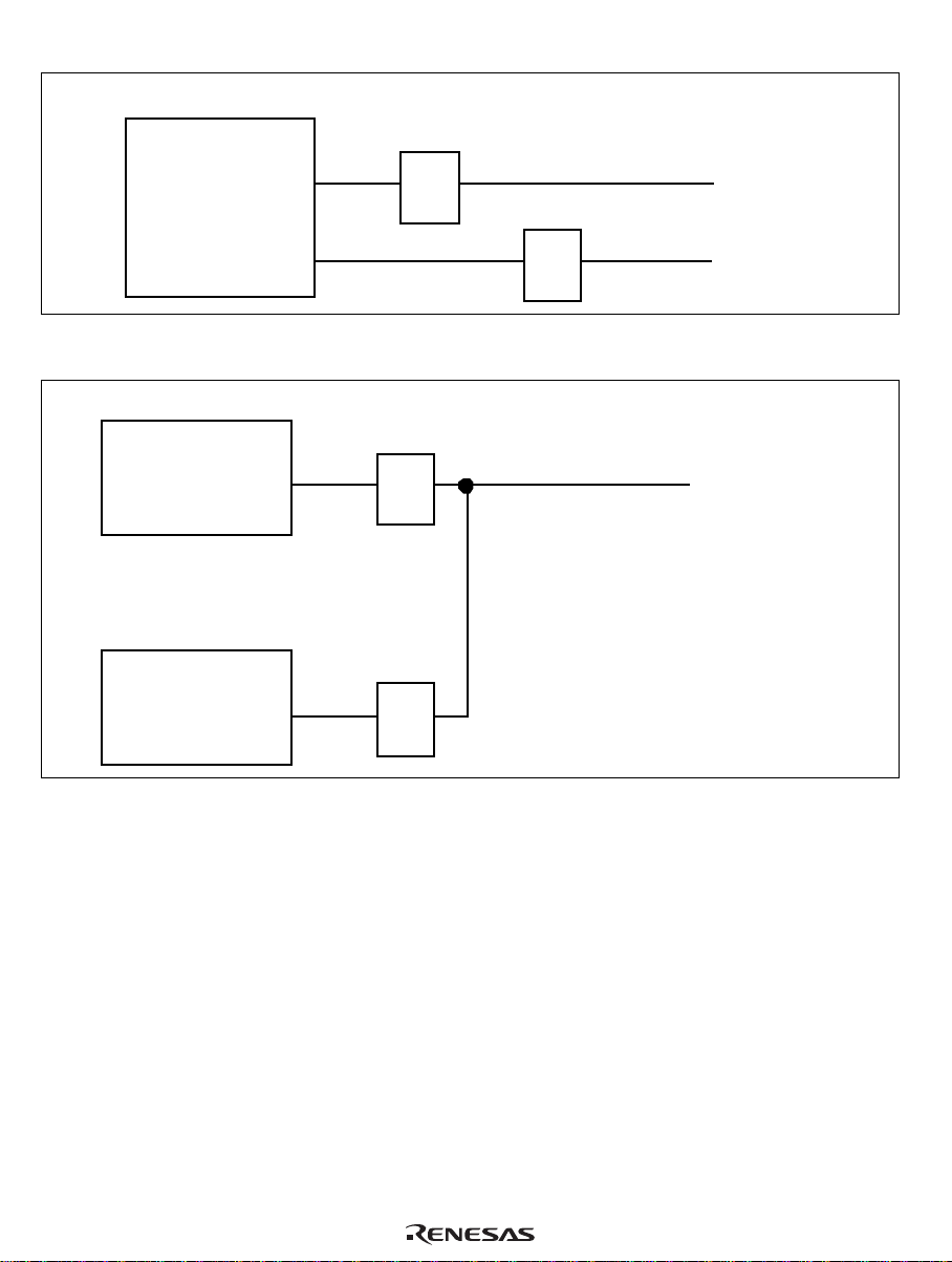
MCU
User system
SN74CB3Q3306A
MCU
Sub-MCU
P23
SN74CB3Q3306A
P27
Figure 11 User System Interface Circuit (2)
SN74CB3Q3306A
P14
SN74CB3Q3306A
TXD
P23
P27
User system
P14
16
Figure 12 User System Interface Circuit (3)
Page 28

MCU
Vcc
User system
_RES
VHC244
EPM7128
UHC14
EPM7128
Figure 13 User System Interface Circuit (4)
47 kΩ
_RES
17
Page 29
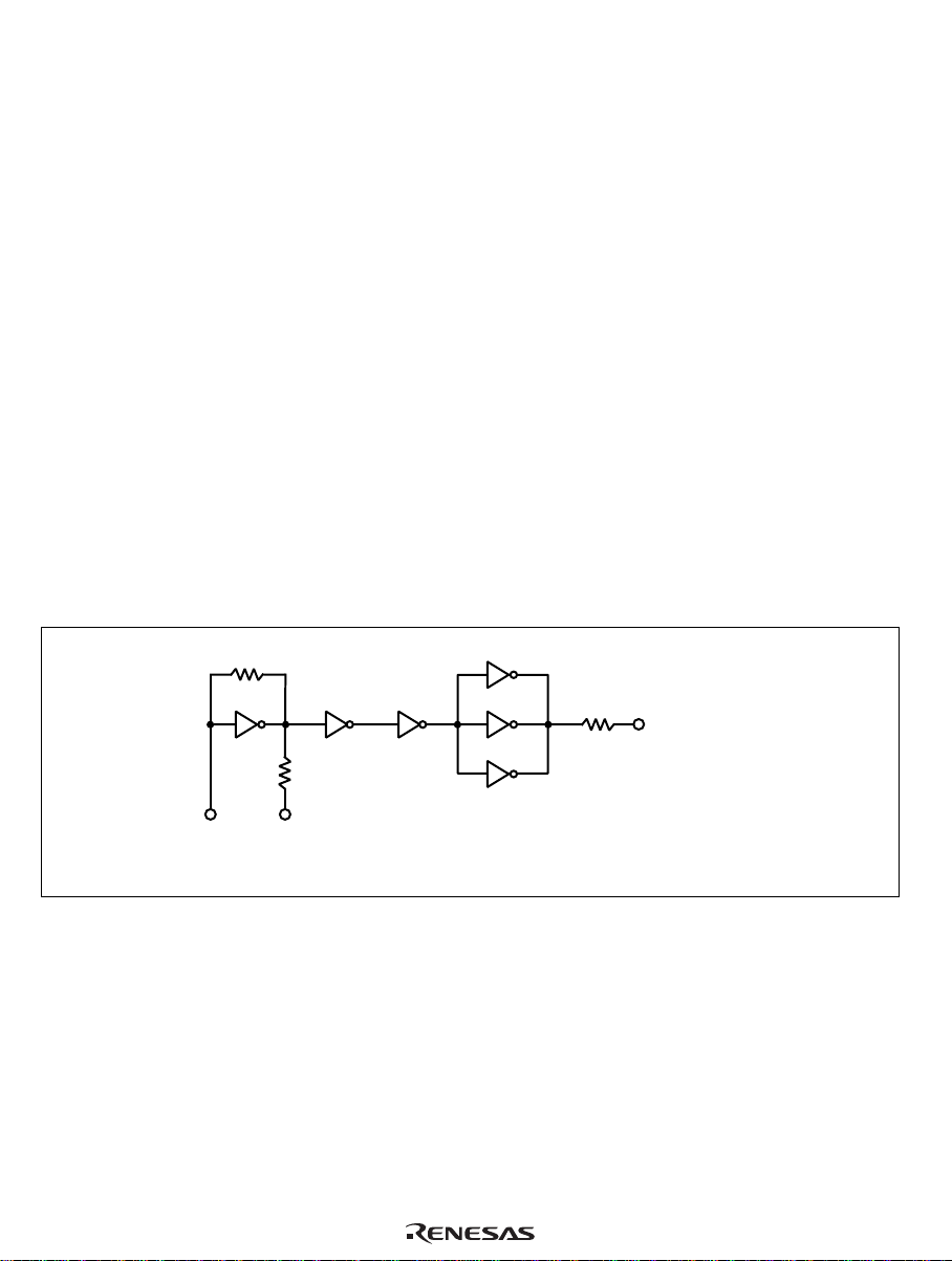
Section 4 Verifying Operation
1. Turn on the emulator according to the procedures described in the H8SX/1650 E6000H
Emulator User's Manual (HS1650EPH60HE).
2. Verify the user system interface cable connections by checking the pin states with the CHECK
command (emulator command) and checking the bus states with the FILL command (emulator
command). If an error is detected, recheck the soldered IC socket and the location of pin 1.
3. The emulator connected to this user system interface board supports three kinds of clock
sources as the MCU clock. For details, refer to the H8SX/1650 E6000H Emulator User's
Manual (HS1650EPH60HE).
To use the emulator internal clock
Select the clock in the emulator by the CLOCK command (emulator command).
To use the external clock on the user system
Supply the external clock from the user system to the emulator by inputting the EXTAL
pin (pin 84) on the user system interface board or connecting the crystal oscillator to the
XTAL (pin 83) and EXTAL pins. For details, refer to the H8SX/1650 Hardware Manual.
Figure 14 shows the clock oscillator on the user system interface board.
18
1 MΩ
HCU04
EXTAL XTAL
System clock
HCU04
HCU04
270 Ω
HCU04
HCU04
HCU04
Figure 14 Clock Oscillator
0 Ω
To E6000H
emulator
Page 30
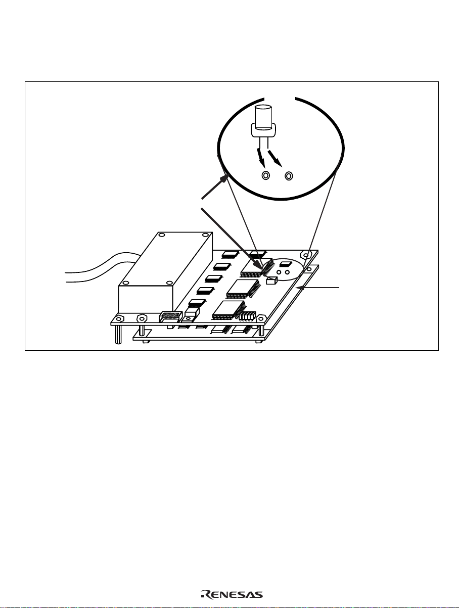
To use the crystal oscillator mounted on the evaluation chip board
Install the crystal oscillator into the crystal oscillato r terminals on the evaluation chip
board.
Enlarged
view
Crystal
oscillator
X1 X2
Crystal oscillator terminals
Evaluation chip
board
Figure 15 Installing the Clock Oscillator
19
Page 31
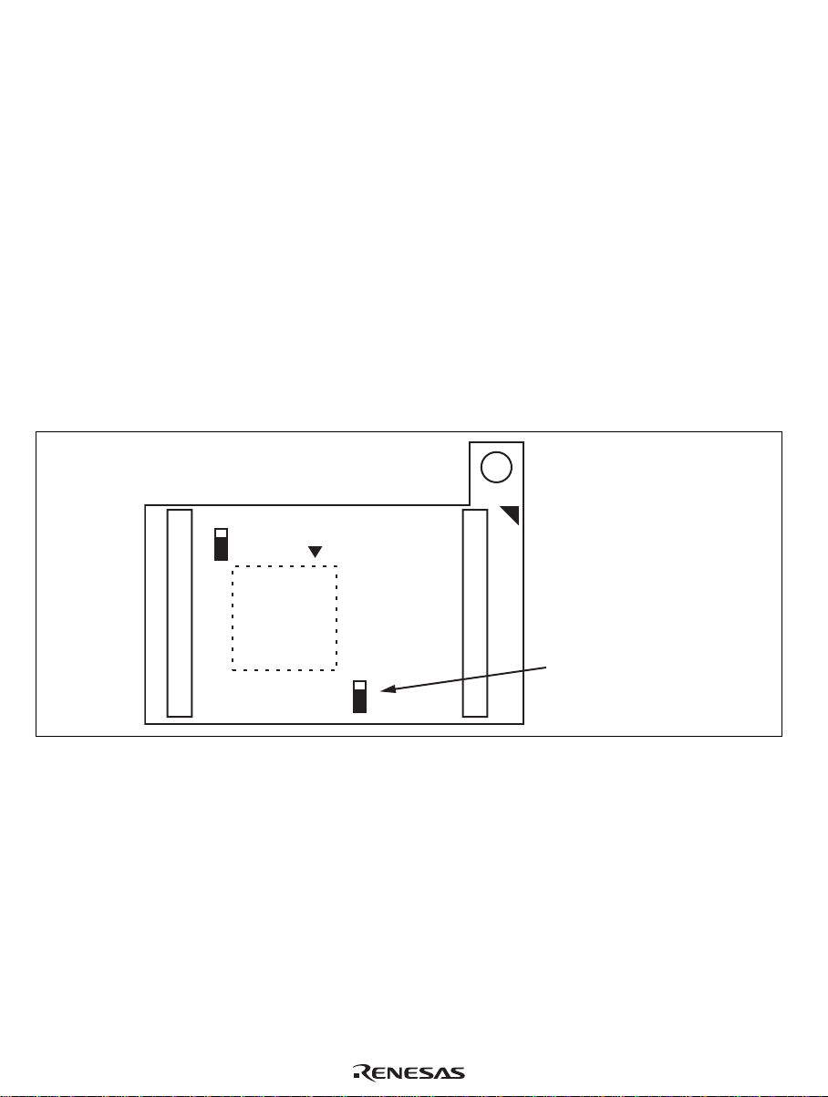
Section 5 Notice
1. Before connecting any parts or cables, make sure that pin 1 on the both sides are correctly
aligned.
2. Do not apply excessive force to the user system interface board while it is connected to the
user system.
3. The dimensions of the recommended mount pad for the IC socket for this user system interface
board are different from those of the MCU.
4. This user system interface board is specifically designed for the HS1650EPH60H emulator.
Do not use this board with any other emulator.
5. When power is not supplied to the Vcc pin on the user system interface board, the emulator
displays ** VCC DOWN. The emulator will not oper a te co rrectly.
6. The P1 jumper socket is used for testing. Do not remove the inserted jumper pin.
OFF
SW1
ON
USER
Do not remove the
3
P1
1
jumper pin.
Figure 16 Jumper Socket
7. Do not connect this user system interface board to the user system for the H8SX/1650 group.
20
Page 32

8. When this emulator is used without connecting to the user system, ensure that the SW1 jumper
pin is inserted to [OFF]. Failure to do so will damage the emulator product, user system
interface cable, and user system.
9. To connect the emulator to the user system, ensure that the SW1 jumper pin is inserted to
[ON]. Failure to do so will damage the emulator product, user system interface board, and user
system.
10. Do not connect a 5-V signal to any pin, including the USB pins. Incorrect usage will cause
damage to the emulator product, user system interface board, and user system.
21
Page 33

Section 6 Restrictions
There are the following restrictions on emulation of the H8SX/1653 group when the user system
interface board is connected to the emulator.
1. The USB clock frequency is fixed to 48 MHz regardless of the EXTAL input.
2. P14 cannot be used as a port if the serial output function has already been selected. The port
pin state cannot be read from the port register.
22
Page 34

Renesas Microcomputer Development Environment System
User's Manual
H8SX/1653 Group E6000H TFP-120
User System Interface Board HS1653ECN61H
Publication Date: Rev.1.00, November 11, 2004
Rev.2.00, December 9, 2005
Published by: Sales Strategic Planning Div.
Renesas Technology Corp.
Edited by: Customer Support Department
Global Strategic Communication Div.
Renesas Solutions Corp.
© 2005. Renesas Technology Corp., All rights reserved. Printed in Japan.
Page 35

Sales Strategic Planning Div. Nippon Bldg., 2-6-2, Ohte-machi, Chiyoda-ku, Tokyo 100-0004, Japan
RENESAS SALES OFFICES
Refer to "http://www.renesas.com/en/network" for the latest and detailed information.
Renesas Technology America, Inc.
450 Holger Way, San Jose, CA 95134-1368, U.S.A
Tel: <1> (408) 382-7500, Fax: <1> (408) 382-7501
Renesas Technology Europe Limited
Dukes Meadow, Millboard Road, Bourne End, Buckinghamshire, SL8 5FH, U.K.
Tel: <44> (1628) 585-100, Fax: <44> (1628) 585-900
Renesas Technology (Shanghai) Co., Ltd.
Unit 205, AZIA Center, No.133 Yincheng Rd (n), Pudong District, Shanghai 200120, China
Tel: <86> (21) 5877-1818, Fax: <86> (21) 6887-7898
Renesas Technology Hong Kong Ltd.
7th Floor, North Tower, World Finance Centre, Harbour City, 1 Canton Road, Tsimshatsui, Kowloon, Hong Kong
Tel: <852> 2265-6688, Fax: <852> 2730-6071
Renesas Technology Taiwan Co., Ltd.
10th Floor, No.99, Fushing North Road, Taipei, Taiwan
Tel: <886> (2) 2715-2888, Fax: <886> (2) 2713-2999
Renesas Technology Singapore Pte. Ltd.
1 Harbour Front Avenue, #06-10, Keppel Bay Tower, Singapore 098632
Tel: <65> 6213-0200, Fax: <65> 6278-8001
Renesas Technology Korea Co., Ltd.
Kukje Center Bldg. 18th Fl., 191, 2-ka, Hangang-ro, Yongsan-ku, Seoul 140-702, Korea
Tel: <82> (2) 796-3115, Fax: <82> (2) 796-2145
Renesas Technology Malaysia Sdn. Bhd
Unit 906, Block B, Menara Amcorp, Amcorp Trade Centre, No.18, Jalan Persiaran Barat, 46050 Petaling Jaya, Selangor Darul Ehsan, Malaysia
Tel: <603> 7955-9390, Fax: <603> 7955-9510
http://www.renesas.com
Colophon 5.0
Page 36

H8SX/1653 Group E6000H TFP-120
User System Interface Board
HS1653ECN61H User’s Manual
2-6 -2, Ote-machi, Chiyoda-ku, Tokyo,100-0004, Japan
 Loading...