

Page 1
REJ09B0109-0500
The revision list can be viewed directly by
clicking the title page.
The revision list summarizes the locations of
revisions and additions. Details should always
be checked by referring to the relevant text.
H8S/2378, H8S/2378R Group
16
Hardware Manual
Renesas 16-Bit Single-Chip Microcomputer
H8S Family/H8S/2300 Series
Rev. 5.00
Revision Date: Nov 18, 2005
Page 2

Keep safety first in your circuit designs!
1. Renesas Technology Corp. puts the maximum effort into making semiconductor products better and
more reliable, but there is always the possibility that trouble may occur with them. Trouble with
semiconductors may lead to personal injury, fire or property damage.
Remember to give due consideration to safety when making your circuit designs, with appropriate
measures such as (i) placement of substitutive, auxiliary circuits, (ii) use of nonflammable material or
(iii) prevention against any malfunction or mishap.
Notes regarding these materials
1. These materials are intended as a reference to assist our customers in the selection of the Renesas
Technology Corp. product best suited to the customer's application; they do not convey any license
under any intellectual property rights, or any other rights, belonging to Renesas Technology Corp. or
a third party.
2. Renesas Technology Corp. assumes no responsibility for any damage, or infringement of any thirdparty's rights, originating in the use of any product data, diagrams, charts, programs, algorithms, or
circuit application examples contained in these materials.
3. All information contained in these materials, including product data, diagrams, charts, programs and
algorithms represents information on products at the time of publication of these materials, and are
subject to change by Renesas Technology Corp. without notice due to product improvements or
other reasons. It is therefore recommended that customers contact Renesas Technology Corp. or
an authorized Renesas Technology Corp. product distributor for the latest product information
before purchasing a product listed herein.
The information described here may contain technical inaccuracies or typographical errors.
Renesas Technology Corp. assumes no responsibility for any damage, liability, or other loss rising
from these inaccuracies or errors.
Please also pay attention to information published by Renesas Technology Corp. by various means,
including the Renesas Technology Corp. Semiconductor home page (http://www.renesas.com).
4. When using any or all of the information contained in these materials, including product data,
diagrams, charts, programs, and algorithms, please be sure to evaluate all information as a total
system before making a final decision on the applicability of the information and products. Renesas
Technology Corp. assumes no responsibility for any damage, liability or other loss resulting from the
information contained herein.
5. Renesas Technology Corp. semiconductors are not designed or manufactured for use in a device or
system that is used under circumstances in which human life is potentially at stake. Please contact
Renesas Technology Corp. or an authorized Renesas Technology Corp. product distributor when
considering the use of a product contained herein for any specific purposes, such as apparatus or
systems for transportation, vehicular, medical, aerospace, nuclear, or undersea repeater use.
6. The prior written approval of Renesas Technology Corp. is necessary to reprint or reproduce in
whole or in part these materials.
7. If these products or technologies are subject to the Japanese export control restrictions, they must
be exported under a license from the Japanese government and cannot be imported into a country
other than the approved destination.
Any diversion or reexport contrary to the export control laws and regulations of Japan and/or the
country of destination is prohibited.
8. Please contact Renesas Technology Corp. for further details on these materials or the products
contained therein.
Rev. 5.00 Nov 18, 2005 page ii of lxii
Page 3

General Precautions on Handling of Product
1. Treatment of NC Pins
Note: Do not connect anything to the NC pins.
The NC (not connected) pins are either not connected to any of the internal circuitry or are
used as test pins or to reduce noise. If something is connected to the NC pins, the
operation of the LSI is not guaranteed.
2. Treatment of Unused Input Pins
Note: Fix all unused input pins to high or low level.
Generally, the input pins of CMOS products are high-impedance input pins. If unused pins
are in their open states, intermediate levels are induced by noise in the vicinity, a passthrough current flows internally, and a malfunction may occur.
3. Processing before Initialization
Note: When power is first supplied, the product’s state is undefined.
The states of internal circuits are undefined until full power is supplied throughout the
chip and a low level is input on the reset pin. During the period where the states are
undefined, the register settings and the output state of each pin are also undefined. Design
your system so that it does not malfunction because of processing while it is in this
undefined state. For those products which have a reset function, reset the LSI immediately
after the power supply has been turned on.
4. Prohibition of Access to Undefined or Reserved Addresses
Note: Access to undefined or reserved addresses is prohibited.
The undefined or reserved addresses may be used to expand functions, or test registers
may have been be allocated to these addresses. Do not access these registers; the system’s
operation is not guaranteed if they are accessed.
Rev. 5.00 Nov 18, 2005 page iii of lxii
Page 4

Configuration of This Manual
This manual comprises the following items:
1. General Precautions on Handling of Product
2. Configuration of This Manual
3. Preface
4. Main Revisions and Additions in this Edition (only for revised versions)
5. Contents
6. Overview
7. Description of Functional Modules
• CPU and System-Control Modules
• On-Chip Peripheral Modules
The configuration of the functional description of each module differs according to the
module. However, the generic style includes the following items:
i) Feature
ii) Input/Output Pin
iii) Register Description
iv) Operation
v) Usage Note
When designing an application system that includes this LSI, take notes into account. Each section
includes notes in relation to the descriptions given, and usage notes are given, as required, as the
final part of each section.
8. List of Registers
9. Electrical Characteristics
10.Appendix
The list of revisions is a summary of points that have been revised or added to earlier versions.
This does not include all of the revised contents. For details, see the actual locations in this
manual.
11.Index
Rev. 5.00 Nov 18, 2005 page iv of lxii
Page 5

Preface
The H8S/2378 Group and H8S/2378R Group microcomputers (MCU) made up of the H8S/2000
CPU employing Renesas Technology's original architecture as their cores, and the peripheral
functions required to con fig ure a sys tem.
The H8S/2000 CPU has an internal 32-bit configuration, sixteen 16-bit general registers, and a
simple and optimized instruction set for high-speed operation. The H8S/2000 CPU can handle a
16-Mbyte linear address space.
This LSI is equipped with direct memory access controller (DMAC and EXDMAC) and data
transfer controller (DTC) bus masters, ROM and RAM memory, a 16-bit timer pulse unit (TPU), a
programmable pulse generator (PPG), an 8-bit timer (TMR), a watchdog timer (WDT), a serial
communication interface (SCI and IrDA), a 10-bit A/D converter, an 8-bit D/A converter, and I/O
ports as on-chip peripheral modules required for system configuration. I
can also be included as an optional interface.
A high functionality bus controller is also provided, enabling fast and easy connection of DRAM
and other kinds of memory.
TM
*
A single-power flash memory (F-ZTAT
) version is available for this LSI's ROM. The F-ZTAT
version provides flexibility as it can be reprogrammed in no time to cope with all situations from
the early stages of mass production to full-scale mass production. This is particularly applicable to
application devices with specifications that will most probably change.
2
C bus interface 2 (IIC2)
This manual describes this LSI's hardware.
Note: * F-ZTAT is a trademark of Renesas Technology Corp.
Target Users: This manual was written for users who will be using this LSI in the design of
application systems. Target users are expected to understand the fundamentals of
electrical circuits, logical circuits, and microcomputers.
Objective: This manual was written to explain the hardware functions and electrical
characteristics of this LSI to the target users.
Refer to the H8S/2600 Series, H8S/2000 Series Programming Manual for a
detailed description of the instru ction se t.
Notes on reading this manual:
In order to understand the overall functions of the chip
Read the manual according to the contents. This manual can be roughly categorized into parts
on the CPU, system control functions, peripheral functions and electrical characteristics.
Rev. 5.00 Nov 18, 2005 page v of lxii
Page 6
In order to understand the details of the CPU's functions
Read the H8S/2600 Series, H8S/2000 Series Programming Manual.
For the execution state of each instruction in this LSI, see Appendix D, Bus State during
Execution of Instructions.
In order to understand the details of a register when its name is known
Read the index that is the final part of the manual to find the page number of the entry on the
register. The addresses, bits, and initial values of the registers are summarized in section 25,
List of Registers.
Examples: Register name: The following notation is used for cases when the same or a
similar function, e.g. 16-bit timer pulse unit or serial
communication, is implemented on more than one channel:
XXX_N (XXX is the register name and N is the channel
number)
Bit order: The MSB is on the left and the LSB is on the right.
Number notation: Binary is B'xxxx, hexadecimal is H'xxxx, decimal is xxxx.
Signal notation: An overbar is added to a low-active signal:
xxxx
Related Manuals: The latest versions of all related manuals are available from our web site.
Please ensure you have the latest versions of all documents you require.
http://www.renesas.com/
H8S/2378 Group and H8S/2378R Group manuals:
Manual Title Document No.
H8S/2378 Group,H8S/2378R Group Hardware Manual This manual
H8S/2600 Series, H8S/2000 Series Programming Manual REJ09B0139-0300O
User's manuals for development tools:
Manual Title Document No.
H8S, H8/300 Series C/C++ Compiler, Assembler, Optimizing Linkage
Editor User's Manual
H8S, H8/300 Series Simulator/Debugger User's Manual REJ10B0211-0200
H8S, H8/300 Series High-performance Embedded Workshop,
High-performance Debugging Interface Tutorial
High-performance Embedded Workshop User's Manual REJ10J0886-0300
Rev. 5.00 Nov 18, 2005 page vi of lxii
REJ10B0058-0100H
ADE-702-231
Page 7
Main Revisions for this Edition
Item Page Revisions (See Manual for Details)
All LGA package newly added
1.1 Features 1 Description amended
• On-chip memory
ROM Type Model
Flash memory version HD64F2378B
2 • General I/O ports
I/O pins:
Input-only pins: 17
• Compact package
Package (Code) Body Size Pin Pitch
FP-144 FP-144H (FP-144HV*) 22.0
LGA-145 TLP-145V
96
*
× 22.0 mm 0.5 mm
9.0 × 9.0 mm 0.65 mm
1.3.1 Pin Arrangement
Figure 1.11 Pin
Arrangement (TLP145V: Top View)
1.3.2 Pin Arrangement
in Each Operating
Mode
Table 1.1 Pin
Arrangement in Each
Operating Mode
1.3.3 Pin Functions
Table 1.2 Pin
Functions
4.6 Trap Instruction
Exception Handling
Table 4.4 Status of
CCR and EXR after
Trap Instruction
Exception Handling
13 Newly added
14 to 19 LGA-145 added, Pin No. 145 added
20 to 34 LGA-145 added
93 Table amended
Interrupt Control Mode
0
2 0
I2 to I0 T
EXR
Rev. 5.00 Nov 18, 2005 page vii of lxii
Page 8
Item Page Revisions (See Manual for Details)
7.4.2 Activation by
External Request
303 Note * added
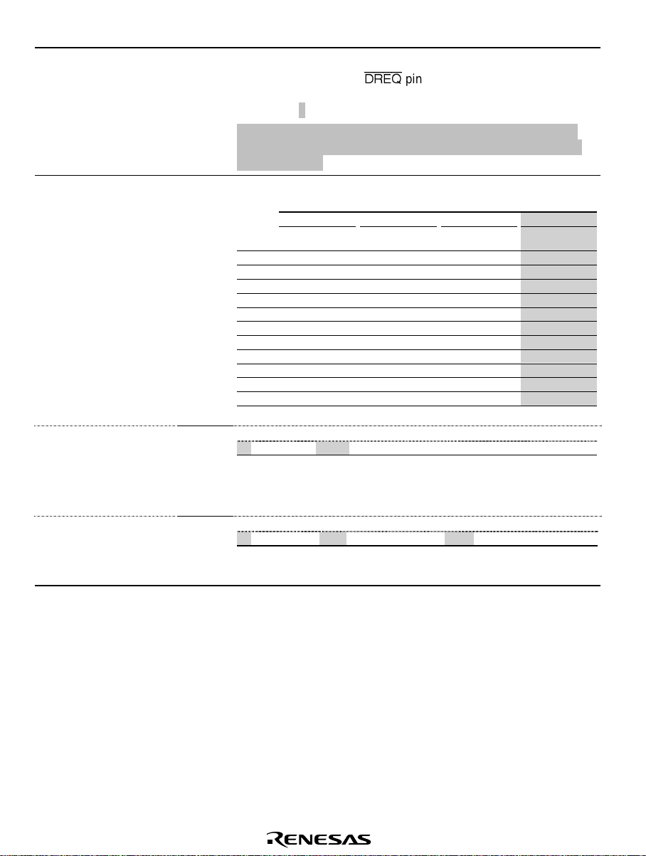
If an external request (
DREQ
pin) is specified as a DMAC
activation source, the relevant port should be set to input mode
in advance*.
Note: * If the relevant port is set as an output pin for another
function, DMA transfers using the channel in question cannot
be guaranteed.
15.3.9 Bit Rate
Register (BRR)
Table 15.3 BBR
Settings for Various Bit
Rates (Asynchronous
Mode)
Table 15.4 Maximum
Bit Rate for Each
747 Table amended
25 30 33
Bit Rate
(bit/s)
nN
110
3 110 –0.02 3 132 0.13 3 145 0.33 3 154 0.23
150
3 80 –0.47 3 97 –0.35 3 106 0.39 3 113 –0.06
300
2 162 0.15 2 194 0.16 2 214 –0.07 2 227 –0.06
600
2 80 –0.47 2 97 –0.35 2 106 0.39 2 113 –0.06
1200
1 162 0.15 1 194 0.16 1 214 –0.07 1 227 –0.06
2400
1 80 –0.47 1 97 –0.35 1 106 0.39 1 113 –0.06
4800
0 162 0.15 0 194 0.16 0 214 –0.07 0 227 –0.06
9600
0 80 –0.47 0 97 –0.35 0 106 0.39 0 113 –0.06
19200
0 40 –0.76 0 48 –0.35 0 53 –0.54 0 56 –0.06
31250
0 24 0.00 0 29 0.00 0 32 0.00 0 34 0.00
38400
0 19 1.73 0 23 1.73 0 26 –0.54 0 27 1.73
Note: * Supported on the H8S/2378 and H8S/2378R only.
748
φ (MHz) Maximum Bit Rate (bit/s) n N
*
35
Operating Frequency φ (MHz)
Error
nn
(%)
1093750 0 0
N
Error
(%) N
Frequency
(Asynchronous Mode)
Error
(%)
n N
*
35
Error
(%)
Table 15.5 Maximum
Bit Rate with External
749
φ (MHz) External Input Clock (MHz) Maximum Bit Rate (bit/s)
*
35
Clock Input
(Asynchronous Mode)
Rev. 5.00 Nov 18, 2005 page viii of lxii
8.7500 546875
Page 9
Item Page Revisions (See Manual for Details)
15.3.9 Bit Rate
Register (BRR)
Table 15.6 BRR
Settings for Various Bit
Rates (Clocked
Synchronous Mode)
750
Table amended
Operating Frequency φ (MHz)
Bit Rate
(bit/s)
110
250 3 124 —— 3 249
500 2 249 —— 3 124 —— 3 233
1 k 2 124 —— 2 249 —— 3 97 3 116 3 128 3 136
2.5 k 1 199 1 249 2 99 2 124 2 155 2 187 2 205 2 218
5 k 1 99 1 124 1 199 1 249 2 77 2 93 2 102 2 108
10 k 0 199 0 249 1 99 1 124 1 155 1 187 1 205 1 218
25 k 0 79 0 99 0 159 0 199 0 249 1 74 1 82 1 87
50 k 0 39 0 49 0 79 0 99 0 124 0 149 0 164 0 174
100 k 0 19 0 24 0 39 0 49 0 62 0 74 0 82 0 87
250 k 0 7 0 9 0 15 0 19 0 24 0 29 0 32 0 34
500 k 0 3 0 4 0 7 0 9 —— 014 —— —
1 M 0 1 0 3 0 4 —— —— —— ———
2.5 M 0 0
5 M 0*—— —— —— ——
8101620253033
nN nN nN nN nN nN nN nN
*
01 —— 02 —— ——
0
1
*
35
Table 15.7 Maximum
Bit Rate with External
Clock Input (Clocked
Synchronous Mode)
Table 15.8 Examples
of Bit Rate for Various
BRR Settings (Smart
Card Interface Mode)
(when n = 0 and S =
372)
Table 15.9 Maximum
Bit Rate at Various
Frequencies (Smart
Card Interface Mode)
(when S = 372)
751
752
φ (MHz)
External Input
Clock (MHz)
Maximum Bit
Rate (bit/s)
20 3.3333 3333333.3
25 4.1667 4166666.7
30 5.0000 5000000.0
33 5.5000 5500000.0
*
35
Bit Rate
(bit/s)
9600 0 3 5.01 0 4 7.59 0 4 1.99
5.8336 5833625.0
Operating Frequency φ (MHz)
30.00 33.00
nN
Error
(%) n N
Error
(%) n N
35.00
*
Error
(%)
Maximum Bit
φ (MHz)
Rate (bit/s) n N
20.00 26882 0 0
25.00 33602 0 0
30.00 40323 0 0
33.00 44355 0 0
*
35.00
47043 0 0
Rev. 5.00 Nov 18, 2005 page ix of lxii
Page 10
Item Page Revisions (See Manual for Details)
15.8 IrDA Operation
Table 15.12 Settings
of Bits IrCKS2 to
IrCKS0
794 Table amended
Operating
Frequency
φ (MHz) 78.13 19.53 9.77 4.88 3.26 1.63
*
35
2400 9600 19200 38400 57600 115200
110 110 110 110 110 —
Bit Rate (bps) (Above)/Bit Period × 3/16 (µs) (Below)
Section 16 I2C Bus
Interface 2 (IIC2)
(Option)
16.3.1 I2C Bus Control
Register A (ICCRA)
Table 16.2 Transfer
Rate
805 Description of 2. deleted
810 Table amended
Bit 3 Bit 2 Bit 1 Bit 0 Transfer Rate
CKS3 CKS2 CKS1 CKS0
0
0
1
1
1
0
1
1
1
1
Clock
0 φ/28 286 kHz 357 kHz 714 kHz 893 kHz 1179 kHz 1250 kHz0
1 φ/40 200 kHz 250 kHz 500 kHz 625 kHz 825 kHz
0 φ/48 167 kHz 208 kHz 417 kHz 521 kHz 688 kHz 729 kHz
1 φ/64 125 kHz 156 kHz 313 kHz 391 kHz 516 kHz
0 φ/168 47.6 kHz 59.5 kHz 119 kHz 149 kHz 196 kHz 208 kHz0
1 φ/100 80.0 kHz 100 kHz 200 kHz 250 kHz 330 kHz
0 φ/112 71.4 kHz 89.3 kHz 179 kHz 223 kHz 295 kHz 313 kHz
1 φ/128 62.5 kHz 78.1 kHz 156 kHz 195 kHz 258 kHz
0 φ/56 143 kHz 179 kHz 357 kHz 446 kHz 589 kHz 625 kHz0
1 φ/80 100 kHz 125 kHz 250 kHz 313 kHz 413 kHz
0 φ/96 83.3 kHz 104 kHz 208 kHz 260 kHz 344 kHz 365 kHz
1 φ/128 62.5 kHz 78.1 kHz 156 kHz 195 kHz 258 kHz
0 φ/336 23.8 kHz 29.8 kHz 59.5 kHz 74.4 kHz 98.2 kHz 104 kHz0
1 φ/200 40.0 kHz 50.0 kHz 100 kHz 125 kHz 165 kHz
0 φ/224 35.7 kHz 44.6 kHz 89.3 kHz 112 kHz 147 kHz 156 kHz
1 φ/256 31.3 kHz 39.1 kHz 78.1 kHz 97.7 kHz 129 kHz
φ =
8 MHz
φ =
10 MHz
φ =
20 MHz
φ =
25 MHz
φ =
33 MHz
φ =
35 MHz
875 kHz
547 kHz
350 kHz
273 kHz
438 kHz
273 kHz
175 kHz
137 kHz
*
Rev. 5.00 Nov 18, 2005 page x of lxii
Page 11
Item Page Revisions (See Manual for Details)
2
16.3.5 I
C Bus Status
Register (ICSR)
817 Table amended
Bit
Initial
Bit
Name
Value R/W Description
3 STOP 0 R/W Stop condition detection flag
[Setting condition]
•
In master mode, when a stop
condition is detected after frame
transfer
•In slave mode, when a stop
condition is detected after the
general call address or the first
byte slave address, next to
detection of start condition,
accords with the address set in
SAR
[Clearing condition]
•When 0 is written in STOP after
reading STOP = 1
16.7 Usage Notes 837 Newly added
17.1 Features 839 Description amended
— Conversion time: 7.4 µs per channel (at 35 MHz operation)
21.1 Features 897
Description of User branch function added
21.3.2 Programming/
Erasing Interface
Parameter
Table 21.4 Parameter
and Target Modes
915, 916 Description amended
When download, initialization, or on-chip program is executed,
registers of the CPU except for ER0 and ER1 are stored.
Table amended
Name of
Parameter
Flash
programm ing/
erasing frequency
control
Flash user bra nch
address set
Flash multi purpose addr ess
area
Flash multi purpose data
destinatio n area
Abbrevi a-
Down
tion
Load
FPEFEQ
—
—
FUBRA
—
FMPAR R/W Undefined ER1 of
—
FMPDR R/W Undefined ER0 of
Initializa-
Program-
tion
ming Er asure R/W
—
—
—
—
—
—
—
—
Initial
Value
R/W Undefined ER0 of
R/W Undefined ER1 of
Allocation
CPU
CPU
CPU
CPU
Rev. 5.00 Nov 18, 2005 page xi of lxii
Page 12
Item Page Revisions (See Manual for Details)
21.3.2 Programming/
Erasing Interface
Parameter
(2) Programming/
Erasing Initialization
918 (a) Flash programming/erasing frequency parameter (FPEFEQ:
general resister ER0 of CPU)
Description amended
This parameter sets the operating frequency of the CPU and
enables the user branch function.
Bit
Bit
Name
FUBF15 to
31 to
FUBF0
16
15 to 0 F15 to F0 — R/W Frequency Set
Initial
Value R/W Description
—
R/W Set to H'AAFF if the user branch function is enabled by
the flash user branch enable bit. Otherwise, set to
H'0000.
Set the operating frequency of the CPU. The setting
value must be calculated as the following methods.
1. The operating frequency which is shown in MHz
units must be rounded in a number to three decimal
places and be shown in a number of two decimal
places.
2. The value multiplied by 100 is converted to the
binary digit and is written to the FPEFEQ parameter
(general register ER0).
For example, when the operating frequency of the CPU
35.000 MHz, the value is as follows.
is
1. The number to three decimal places of 35.000 is
rounded and the value is thus
2. The formula that 35.00 × 100 = 3500 is converted to
the binary digit and B'0000,1101,
H'0DAC) is set to R0.
(
919 (b) Flash user branch address setting parameter (FUBRA:
general register ER1 of CPU)
Added
920
(c) Flash pass/fail parameter (FPFR: general register R0L of
CPU)
Table amended
Bit
Bit
Initial
Name
Value R/W Description
7 to 3 Unused
Return 0
2 BR R/W User Branch Error Detect (BR)
Returns the check result
whether the specified user
branch destination address is in
the area other than the storage
area of the programmi ng/erasing
program which has been
downloaded.
0: User branch address setting
is normal
1: User branch address setting
is abnormal
35.00.
1010,1100
Rev. 5.00 Nov 18, 2005 page xii of lxii
Page 13
Item Page Revisions (See Manual for Details)
21.3.2 Programming/
Erasing Interface
Parameter
(2) Programming/
Erasing Initialization
922 (3) Programming Execution
(c) Flash pass/fail parameter (FPFR: general register R0L of
CPU)
Table amended
Bit
Bit
Initial
Name
Value R/W Description
5EE R/W Programming Execution Error
Detect
1 is returned to this bit when the
specified data could not be
written because the user MAT
was not erased or when flashmemory related register settings
are partially changed on
returning from the user branch
processing. If this bit is set to 1,
there is a high possibility that the
user MAT is partially rewritten.
In this case, after removing the
error factor, erase the user MAT.
If FMATS is set to H'AA and the
user boot MAT is selected, an
error occurs when programming
is performed. In this case, both
the user MAT and user boot
MAT are not rewritten.
Programming of the user boot
MAT should be performed in
boot mode or PROM mode.
0: Programming has ended
1: Programming has ended
normally
abnormally (programmi ng
result is not guaranteed)
(4) Erasur e Execution 924 (a) Flash erase blo ck select parameter (FEBS: general register
ER0 of CPU)
Description amended
This parameter specifies the erase-block number.
Bit
Bit
7 to 0 EBN7 to
Initial
Name
Value R/W Description
— R/W Erase Block Number
EBN0
Set an erase-block number within the range from 0 to 15.
H'00 corresponds to the EB0 block and H'0F
corresponds to the EB15 block. An error occurs if a
number outside the range from H'00 to H'0F is set..
Rev. 5.00 Nov 18, 2005 page xiii of lxii
Page 14

Item Page Revisions (See Manual for Details)
21.3.2 Programming/
Erasing Interface
Parameter
(4) Erasure Execution
924, 925 (b) Flash pass/fail parameter (FPFR: general register R0L of
CPU)
Table amended
Bit
Bit
6
5EE R/W Erasure Execution Error Detect
Initial
Name
Value R/W Description
MD R/W Programming Mode Related
Setting Error Detect
Returns the check result of
whether the error protection
state is entered. The error
protection state is entered, 1 is
written to this bit. The error
protection state can be
confirmed with the FLER bit in
FCCS. For conditions to enter
the error protection state, see
section 21.5.3, Error Protection.
0: FLER setting is normal
(FLER = 0)
1: FLER = 1 and programming
cannot be performed
1 is returned to this bit when the
user MAT could not be erased
or when flash-memory related
register settings are partially
changed
user branch processing. If this
bit is set to 1, there is a high
possibility that the user MAT is
partially erased. In this case,
after removing the error factor,
erase the user MAT. If FMATS
is set to H'AA and the user boot
MAT is selected, an error occurs
when erasure is performed. In
this case, both the user MAT
and user boot MAT are not
erased. Erasing of the user boot
MAT should be performed in
boot mode or PROM mode.
0: Erasure has ended normally
1: Erasure has ended
on returning from the
abnormally (erasure result is
not guaranteed)
Rev. 5.00 Nov 18, 2005 page xiv of lxii
Page 15

Item Page Revisions (See Manual for Details)
21.4.2 User Program
933 Figure amended
Mode
(2) Programming
Procedure in User
Program Mode
Figure 21.11
Programming
Procedure
DPFR = 0?
Set the FPEFEQ, FUBRA
parameter
Initialization
JSR FTDAR setting + 32
Initialization
FPFR = 0?
Yes
Yes
a
5.
No
Download error processing
6.
7.
8.
No
Initialization error processing
936 Description amended
6.The FPEFEQ and FUBRA parameters are set for
initialization.
The allowable setting range for the FPEFEQ parameter is 8
MHz to 35 MHz. When the ...
— Set the user branch destination address as the FUBRA
parameter (general register ER1) and the user branch enable
bits (FUBE15 to FUBE0) as the FPEFEQ parameter (general
register ER0). Set FUBRA and FUBE15 to FUBE0 to 0 if the
user branch function is not required.
Do use programmable user MAT as the user branch
destination. Also, do not use an area containing a downloaded
internal program as the user branch destination. After user
branch processing completes, use the RTS instruction to return
to programming processing.
For details, see the descriptions in 21.3.2 (2) (a), Flash
programming/erasing frequency parameter (FPEFEQ), and
21.3.2 (2) (b), Flash user branch address setting parameter
(FUBRA).
— The general registers other than ER0, ER1 are held in the
initialization program.
FPFR = 0?
Yes
Required data
No
programming is
completed?
Yes
Programming finished
processing
JSR FTDAR setting + 16
FPFR = 0?
Yes
Clear FKEY to 0
End programming
procedure program
13.
No
Clear FKEY and
programming
error processing
14.
15.
16.
No
Clear FKEY and
programming
error processing
17.
Rev. 5.00 Nov 18, 2005 page xv of lxii
Page 16
Item Page Revisions (See Manual for Details)
21.4.2 User Program
Mode
(2) Programming
Procedure in User
Program Mode
938, 939 Description amended
12. Programming
The general registers other than ER0 and ER1 are held in
the programming program.
15. Execution of Programming Finished Processing
— Data is stored in a general register other than ER0, ER1 by
the programming finished program.
:
— Only perform programming finished processing once per
block. Even if multiple 128-byte programming operations have
been performed to the same block, programming finished
processing should only be carried out once. (Due not perform
programming finished processing multiple times.) If it is
necessary to reprogram blocks within a previously programmed
area on which programming finished processing has been
performed, first erase the blocks in question and then
reprogram them.
— Programming finished processing should be performed on
all blocks containing areas that have been programmed after
initialization processing. For example, if programming finished
processing is to be carried out once after programming blocks
EB1 to EB3, programming finished processing should be
performed individually on EB1, EB2, and EB3.
939 Description added
16. Determine the FPFR (general-purpose register R0L) value
returned by the programming program.
(3) Erasing Procedure
940 Figure amended
in User Program Mode
Figure 21.12 Erasing
Procedure
Set the FPEFEQ, FUBRA
parameter
Initialization
JSR FTDAR setting
+ 32
941 Description amended
• The general registers other than ER0, ER1 are held in the
erasing program.
Rev. 5.00 Nov 18, 2005 page xvi of lxii
Page 17
Item Page Revisions (See Manual for Details)
21.4.3 User Boot
943 Figure amended
Mode
Figure 21.13
Procedure for
Programming finished
processing
JSR FTDAR setting + 16
Programming User
MAT in User Boot Mode
FPFR = 0 ?
Yes
Clear FKEY to 0
No
Clear FKEY and programming
error processing*
Set FMATS to H'AA to
select user boot MAT
End programming
procedure program
21.8 Serial
Communication
Interface Specification
for Boot Mode
(4) Inquiry and
Selection States
966
(c) Clock Mode Inquiry
Description amended
Response H'31 Size Mode ··· SUM
• Response, H'31, (one byte): Response to the clock-mode
inquiry
• Size (one byte): Amount of data that represents modes
21.9 Usage Notes 988 Description amended
The programming … or less. Accordingly, when the CPU clock
frequency is 35 MHz, …
23.5.1 Notes on Clock
Pulse Generator
998 Note amended
Note: * 35 MHz for the H8S/2378 and H8S/2378R
MAT
switchover
Rev. 5.00 Nov 18, 2005 page xvii of lxii
Page 18
Item Page Revisions (See Manual for Details)
24.2.3 Software
Standby Mode
Table 24.2 Oscillation
Stabilization Time
Settings
1011 Table amended
STS3 STS2 STS1 STS0
0000Reserved ———————µs
1 Reserved ———————
1 0 Reserved ———————
1 Reserved ———————
100Reserved ———————
164 1.8 1.9 2.6 3.2 4.9 6.4 8.0
1 0 512 15.0 15.5 20.5 25.6 39.4 51.2 64.0
1 1024 29.3 31.0 41.0 51.2 78.8 102.4 128.0
10002048 58.5 62.1 81.9 102.4 157.5 204.8 256.0
1 4096 0.12 0.12 0.16 0.20 0.32 0.41 0.51 ms
1 0 16384 0.47 0.50 0.66 0.82 1.26 1.64 2.05
1 32765 0.94 0.99 1.31 1.64 2.52 3.28 4.10
1 0 0 65536 1.87 1.99 2.62 3.28 5.04 6.55 8.19
1 131072 3.74 3.97 5.24 6.55 10.08 13.11 16.38
1 0 262144 7.49 7.94 10.49 13.11 20.16 26.21 32.77
1 524288 14.98 15.89 20.97 26.21 40.33 52.43 65.54
Standby
Time
2
*
35
33 25 20 13 10 8 Unit
φ
1
*
[MHz]
26.2.2 DC
Characteristics
Table 26.15 DC
Characteristics
Table 26.16 DC
Characteristics
Table 26.17
Permissible Output
Currents
1072 Table amended and Note *4 added
Item Symbol Min. Typ. Max. Unit
voltage
All output pins V
P32 to P34
4
*
— 0.4 V IOL = 1.6 mAOutput low
OL
— ——0.5 V IOL = 8.0 mA
Notes: 4. When used as SCL0, SCL1, SDA0, and SDA1.
1074 Table amended and Note *5 added
Item Symbol Min. Typ. Max. Unit
VCC start voltage
VCC rise slope
Notes: 5. Applies when
5
*
5
*
V
— — V
CCstart
SV
— — ms/V
CC
RES
pin is low level at power-on.
Table amended
Item Symbol Min. Typ. Max. Unit
I
current (per pin)
all output pins
IIC output pins — — 8.0
OL
Test
Conditions
Test
0.8
20
——2.0 mAPermissible output low Other than IIC pins
Conditions
Rev. 5.00 Nov 18, 2005 page xviii of lxii
Page 19
Item Page Revisions (See Manual for Details)
26.2.3 AC
Characteristics
Table 26.18 Clock
Timing
1075 Table amended
Conditions: …φ = 8 MHz to
Item Symbol Min. Max. Unit Test Conditions
Clock cycle time t
35 MHz, …
28.5 125 ns Figure 26.2
cyc
Table 26.19 Control
Signal Timing
Table 26.20 Bus
Timing (1)
Table 26.21 Bus
Timing (2)
Table 26.22 DMAC
and EXDMAC Timing
Table 26.23 Timing of
On-Chip Peripheral
Modules
26.2.4 A/D Conversion
Characteristics
Table 26.24 A/D
Conversion
Characteristics
26.2.5 D/A Conversion
Characteristics
Table 26.25 D/A
Conversion
Characteristics
1076 Conditions: …φ = 8 MHz to 35 MHz, …
1077
1079 Table amended
35 MHz, …
25 — ns
WTS
1 — ns
WTH
1080
Conditions: …φ = 8 MHz to
Item Symbol Min. Max. Unit Test Conditions
WAIT setup time t
WAIT hold time t
1081 Conditions: …φ = 8 MHz to 35 MHz, …
1082
1084 Table amended
Conditions: …φ = 8 MHz to 35 MHz, …
Item Min. Typ. Max. Unit
Resolution 10 10 10 Bit
Conversion time 7.4 —— µs
Conditions: …φ = 8 MHz to 35 MHz, …
Figures 26.9 and
26.15
Rev. 5.00 Nov 18, 2005 page xix of lxii
Page 20
Item Page Revisions (See Manual for Details)
B. Product Lineup 1125 Table amended
Product Type Name Model Marking
H8S/2378
Group
H8S/2378 F-ZTAT
version
H8S/2377 HD64F2377 HD64F2377VFQ
H8S/2376 HD6432376 HD6432376VFQ
HD64F2378
Package
B HD64F2378B 144-pin LGA
HD64F2378BVFQ
(Code)
(TLP-145V*)
144-pin QFP
(FP-144H,
FP144HV*)
C Package
Dimensions
Figure C.2 Package
Dimensions (TLP-145V)
1127 Newly added
Rev. 5.00 Nov 18, 2005 page xx of lxii
Page 21

Contents
Section 1 Over v iew............................................................................................................. 1
1.1 Features............................................................................................................................. 1
1.2 Block Diagram.................................................................................................................. 3
1.3 Pin Description................................................................................................................. 8
1.3.1 Pin Arrangement.............................................................................................. 8
1.3.2 Pin Arrangement in Each Operating Mode...................................................... 14
1.3.3 Pin Functions................................................................................................... 20
Section 2 CPU...................................................................................................................... 35
2.1 Features............................................................................................................................. 35
2.1.1 Differences between H8S/2600 CPU and H8S/2000 CPU.............................. 36
2.1.2 Differences from H8/300 CPU ........................................................................ 37
2.1.3 Differences from H8/300H CPU ..................................................................... 37
2.2 CPU Operating Modes...................................................................................................... 38
2.2.1 Normal Mode................................................................................................... 38
2.2.2 Advanced Mode............................................................................................... 40
2.3 Address Space................................................................................................................... 42
2.4 Register Configuration...................................................................................................... 43
2.4.1 General Registers............................................................................................. 44
2.4.2 Program Counter (PC)..................................................................................... 45
2.4.3 Extended Control Register (EXR)................................................................... 45
2.4.4 Condition-Code Register (CCR)...................................................................... 46
2.4.5 Initial Register Values..................................................................................... 47
2.5 Data Formats..................................................................................................................... 47
2.5.1 General Register Data Formats........................................................................ 48
2.5.2 Memory Data Formats..................................................................................... 50
2.6 Instruction Set................................................................................................................... 51
2.6.1 Table of Instructions Classified by Function................................................... 52
2.6.2 Basic Instruction Formats................................................................................ 61
2.7 Addressing Modes and Effective Address Calculation..................................................... 62
2.7.1 Register Direct—Rn........................................................................................ 63
2.7.2 Register Indirect—@ERn................................................................................ 63
2.7.3 Register Indirect with Displacement—@(d:16, ERn) or @(d:32, ERn).......... 63
2.7.4 Register Indirect with Post-Increm ent or Pre-Dec reme nt
—@ERn+ or @-ERn....................................................................................... 63
2.7.5 Absolute Address—@aa:8, @aa:16, @aa:24, or @aa:32 ............................... 64
2.7.6 Immediate—#xx:8, #xx:16, or #xx:32............................................................. 64
2.7.7 Program-Counter Relative—@(d:8, PC) or @(d:16, PC)............................... 65
Rev. 5.00 Nov 18, 2005 page xxi of lxii
Page 22

2.7.8 Memory Indirect—@@aa:8............................................................................ 65
2.7.9 Effective Address Calculation ......................................................................... 66
2.8 Processing States .............................................................................................................. 68
2.9 Usage Note ....................................................................................................................... 69
2.9.1 Note on Bit Manipulation Instructions ............................................................ 69
Section 3 MCU Ope r ating Modes.................................................................................. 71
3.1 Operating Mode Selection................................................................................................ 71
3.2 Register Descriptions........................................................................................................72
3.2.1 Mode Control Register (MDCR)..................................................................... 72
3.2.2 System Control Register (SYSCR).................................................................. 72
3.3 Operating Mode Descriptions........................................................................................... 75
3.3.1 Mode 1............................................................................................................. 75
3.3.2 Mode 2............................................................................................................. 75
3.3.3 Mode 3............................................................................................................. 75
3.3.4 Mode 4............................................................................................................. 75
3.3.5 Mode 5............................................................................................................. 76
3.3.6 Mode 7............................................................................................................. 76
3.3.7 Pin Functions................................................................................................... 77
3.4 Memory Map in Each Operating Mode............................................................................ 78
Section 4 Exception Handling......................................................................................... 87
4.1 Exception Handling Types and Priority............................................................................ 87
4.2 Exception Sources and Exception Vector Table............................................................... 87
4.3 Reset ................................................................................................................................. 89
4.3.1 Reset Exception Handling............................................................................... 89
4.3.2 Interrupts after Reset........................................................................................ 91
4.3.3 On-Chip Peripheral Functions after Reset Release.......................................... 91
4.4 Trace Exception Handling................................................................................................ 92
4.5 Interrupt Exception Handling ........................................................................................... 92
4.6 Trap Instruction Exception Handling................................................................................ 93
4.7 Stack Status after Exception Handling.............................................................................. 94
4.8 Usage Note ....................................................................................................................... 95
Section 5 Inte r r upt Controller.......................................................................................... 97
5.1 Features............................................................................................................................. 97
5.2 Input/Output Pins.............................................................................................................. 99
5.3 Register Descriptions........................................................................................................99
5.3.1 Interrupt Control Register (INTCR) ................................................................ 100
5.3.2 Interrupt Priority Registers A to K (IPRA to IPRK)........................................ 100
5.3.3 IRQ Enable Register (IER).............................................................................. 102
Rev. 5.00 Nov 18, 2005 page xxii of lxii
Page 23

5.3.4 IRQ Sense Control Registers H and L (ISCRH, ISCRL)................................. 104
5.3.5 IRQ Status Register (ISR)................................................................................ 110
5.3.6 IRQ Pin Select Register (ITSR)....................................................................... 111
5.3.7 Software Standby Release IRQ Enable Register (SSIER)............................... 113
5.4 Interrupt Sources............................................................................................................... 114
5.4.1 External Interrupts........................................................................................... 114
5.4.2 Internal Interrupts............................................................................................ 115
5.5 Interrupt Exception Handling Vector Table...................................................................... 115
5.6 Interrupt Control Modes and Interrupt Operation............................................................. 121
5.6.1 Interrupt Control Mode 0................................................................................. 121
5.6.2 Interrupt Control Mode 2................................................................................. 123
5.6.3 Interrupt Exception Handling Sequence.......................................................... 124
5.6.4 Interrupt Response Times................................................................................ 126
5.6.5 DTC and DMAC Activation by Interrupt........................................................ 127
5.7 Usage Notes...................................................................................................................... 128
5.7.1 Conflict between Interrupt Generation and Disabling..................................... 128
5.7.2 Instructions that Disable Interrupts.................................................................. 129
5.7.3 Times when Interrupts are Disabled................................................................ 129
5.7.4 Interrupts during Execution of EEPMOV Instruction..................................... 129
5.7.5 Change of IRQ Pin Select Register (ITSR) Setting......................................... 129
5.7.6 IRQ Status Register (ISR)................................................................................ 130
Section 6 Bus Co ntr o l ler (BSC)...................................................................................... 131
6.1 Features............................................................................................................................. 131
6.2 Input/Output Pins.............................................................................................................. 133
6.3 Register Descriptions........................................................................................................ 136
6.3.1 Bus Width Control Register (ABWCR)........................................................... 137
6.3.2 Access State Control Register (ASTCR)......................................................... 137
6.3.3 Wait Control Registers AH, AL, BH, and BL
(WTCRAH, WTCRAL, WTCRBH, and WTCRBL) ...................................... 138
6.3.4 Read Strobe Timing Control Register (RDNCR) ............................................ 144
6.3.5
6.3.6 Area 0 Burst ROM Interface Control Register (BROMCRH)
6.3.7 Bus Control Register (BCR)............................................................................ 148
6.3.8 DRAM Control Register (DRAMCR)............................................................. 150
6.3.9 DRAM Access Control Register (DRACCR).................................................. 158
6.3.10 Refresh Control Register (REFCR)................................................................. 161
6.3.11 Refresh Timer Counter (RTCNT).................................................................... 164
6.3.12 Refresh Time Constant Register (RTCOR)..................................................... 164
6.4 Bus Control....................................................................................................................... 165
CS
Assertion Period Control Registers H, L (CSACRH, CSACRL)............... 145
Area 1 Burst ROM Interface Control Register (BROMCRL) ......................... 147
Rev. 5.00 Nov 18, 2005 page xxiii of lxii
Page 24
6.4.1 Area Division................................................................................................... 165
6.4.2 Bus Specifications ........................................................................................... 166
6.4.3 Memory Interfaces........................................................................................... 168
6.4.4 Chip Select Signals.......................................................................................... 169
6.5 Basic Bus Interface........................................................................................................... 170
6.5.1 Data Size and Data Alignment......................................................................... 170
6.5.2 Valid Strobes ................................................................................................... 172
6.5.3 Basic Timing.................................................................................................... 172
6.5.4 Wait Control.................................................................................................... 181
6.5.5 Read Strobe (
6.5.6 Extension of Chip Select (
RD
) Timing................................................................................ 182
CS
) Assertion Period ............................................. 183
6.6 DRAM Interface............................................................................................................... 185
6.6.1 Setting DRAM Space ...................................................................................... 185
6.6.2 Address Multiplexing...................................................................................... 185
6.6.3 Data Bus .......................................................................................................... 186
6.6.4 Pins Used for DRAM Interface ....................................................................... 187
6.6.5 Basic Timing.................................................................................................... 188
6.6.6 Column Address Output Cycle Control........................................................... 189
6.6.7 Row Address Output State Control.................................................................. 190
6.6.8 Precharge State Control................................................................................... 192
6.6.9 Wait Control.................................................................................................... 193
6.6.10 Byte Access Control........................................................................................ 196
6.6.11 Burst Operation................................................................................................ 197
6.6.12 Refresh Control................................................................................................ 202
6.6.13 DMAC and EXDMAC Single Address Transfer Mode and
DRAM Interface.............................................................................................. 207
6.7 Synchronous DRAM Interface......................................................................................... 210
6.7.1 Setting Continuous Synchronous DRAM Space............................................. 210
6.7.2 Address Multiplexing...................................................................................... 211
6.7.3 Data Bus .......................................................................................................... 212
6.7.4 Pins Used for Synchronous DRAM Interface.................................................. 212
6.7.5 Synchronous DRAM Clock............................................................................. 214
6.7.6 Basic Timing.................................................................................................... 214
6.7.7 CAS Latency Control...................................................................................... 216
6.7.8 Row Address Output State Control.................................................................. 218
6.7.9 Precharge State Count...................................................................................... 219
6.7.10 Bus Cycle Control in Write Cycle................................................................... 221
6.7.11 Byte Access Control........................................................................................ 222
6.7.12 Burst Operation................................................................................................ 225
6.7.13 Refresh Control................................................................................................ 228
6.7.14 Mode Register Setting of Synchronous DRAM.............................................. 234
Rev. 5.00 Nov 18, 2005 page xxiv of lxii
Page 25
6.7.15 DMAC and EXDMAC Single Address Transfer Mode and Synchronous
DRAM Interface.............................................................................................. 235
6.8 Burst ROM Interface ........................................................................................................ 240
6.8.1 Basic Timing.................................................................................................... 240
6.8.2 Wait Control.................................................................................................... 242
6.8.3 Write Access.................................................................................................... 242
6.9 Idle Cycle.......................................................................................................................... 243
6.9.1 Operation......................................................................................................... 243
6.9.2 Pin States in Idle Cycle.................................................................................... 262
6.10 Write Data Buffer Function.............................................................................................. 262
6.11 Bus Release....................................................................................................................... 263
6.11.1 Operation......................................................................................................... 264
6.11.2 Pin States in External Bus Released State....................................................... 265
6.11.3 Transiti on Timing............................................................................................ 266
6.12 Bus Arbitration ................................................................................................................. 268
6.12.1 Operation......................................................................................................... 268
6.12.2 Bus Transfe r Timing........................................................................................ 269
6.13 Bus Controller Operation in Reset.................................................................................... 270
6.14 Usage Notes...................................................................................................................... 271
6.14.1 External Bus Release Function and All-Module-Clocks-Stopped Mode......... 271
6.14.2 External Bus Release Function and Software Standby.................................... 271
6.14.3 External Bus Release Function and CBR Refreshing/Auto Refreshing........... 271
6.14.4
6.14.5 Notes on Usage of the Synchronous DRAM................................................... 272
BREQO
Output Timing................................................................................... 272
Section 7 DMA Controller (DMAC)............................................................................. 273
7.1 Features............................................................................................................................. 273
7.2 Input/Output Pins.............................................................................................................. 275
7.3 Register Descriptions........................................................................................................ 275
7.3.1 Memory Address Registers (MARA and MARB)........................................... 277
7.3.2 I/O Address Registers (IOARA and IOARB).................................................. 277
7.3.3 Execute Transfer Count Registers (ETCRA and ETCRB) .............................. 278
7.3.4 DMA Control Registers (DMACRA and DMACRB)..................................... 279
7.3.5 DMA Band Control Registers H and L (DMABCRH and DMABCRL)......... 287
7.3.6 DMA Write Enable Register (DMAWER)...................................................... 298
7.3.7 DMA Terminal Control Register (DMATCR)................................................ 300
7.4 Activation Sources............................................................................................................ 301
7.4.1 Activation by Internal Interrupt Request ......................................................... 302
7.4.2 Activation by External Request....................................................................... 303
7.4.3 Activation by Auto-Request............................................................................ 303
7.5 Operation .......................................................................................................................... 303
Rev. 5.00 Nov 18, 2005 page xxv of lxii
Page 26
7.5.1 Transfer Modes................................................................................................ 303
7.5.2 Sequential Mode.............................................................................................. 306
7.5.3 Idle Mode......................................................................................................... 308
7.5.4 Repeat Mode.................................................................................................... 310
7.5.5 Single Address Mode....................................................................................... 314
7.5.6 Normal Mode................................................................................................... 317
7.5.7 Block Transfer Mode....................................................................................... 320
7.5.8 Basic Bus Cycles............................................................................................. 325
7.5.9 DMA Transfer (Dual Address Mode) Bus Cycles........................................... 326
7.5.10 DMA Transfer (Single Address Mode) Bus Cycles ........................................ 334
7.5.11 Write Data Buffer Function............................................................................. 340
7.5.12 Multi-Channel Operation................................................................................. 341
7.5.13 Relation between DMAC and External Bus Requests, Refresh Cycles,
and EXDMAC................................................................................................. 343
7.5.14 DMAC and NMI Interrupts............................................................................. 344
7.5.15 Forced Termi nation of DMA C Operation....................................................... 345
7.5.16 Clearing Full Address Mode............................................................................ 346
7.6 Interrupt Sources............................................................................................................... 347
7.7 Usage Notes...................................................................................................................... 348
7.7.1 DMAC Register Access during Operation ...................................................... 348
7.7.2 Module Stop .................................................................................................... 349
7.7.3 Write Data Buffer Function............................................................................. 350
7.7.4
7.7.5 Activation by Falling Edge on
7.7.6 Activation Source Acceptance......................................................................... 352
7.7.7 Internal Interrupt after End of Transfer ........................................................... 352
7.7.8 Channel Re-Setting.......................................................................................... 352
TEND
Output .................................................................................................. 350
DREQ
Pin....................................................... 351
Section 8 EXDMA Controller (EXDMAC)................................................................ 353
8.1 Features............................................................................................................................. 353
8.2 Input/Output Pins.............................................................................................................. 355
8.3 Register Descriptions........................................................................................................ 356
8.3.1 EXDMA Source Address Register (EDSAR).................................................. 356
8.3.2 EXDMA Destination Address Register (EDDAR).......................................... 356
8.3.3 EXDMA Transfer Count Register (EDTCR)................................................... 357
8.3.4 EXDMA Mode Control Register (EDMDR)................................................... 359
8.3.5 EXDMA Address Control Register (EDACR)................................................ 364
8.4 Operation .......................................................................................................................... 368
8.4.1 Transfer Modes................................................................................................ 368
8.4.2 Address Modes................................................................................................ 369
8.4.3 DMA Transfer Requests.................................................................................. 373
Rev. 5.00 Nov 18, 2005 page xxvi of lxii
Page 27
8.4.4 Bus Modes....................................................................................................... 373
8.4.5 Transfer Modes................................................................................................ 375
8.4.6 Repeat Area Function...................................................................................... 377
8.4.7 Registers during DMA Transfer Operation ..................................................... 379
8.4.8 Channel Priority Order .................................................................................... 384
8.4.9 EXDMAC Bus Cycles (Dual Address Mode)................................................. 387
8.4.10 EXDMAC Bus Cycles (Single Address Mode)............................................... 394
8.4.11 Examples of Operation Timing in Each Mode ................................................ 399
8.4.12 Ending DMA Transfer..................................................................................... 412
8.4.13 Relationship between EXDMAC and Other Bus Masters............................... 413
8.5 Interrupt Sources............................................................................................................... 414
8.6 Usage Notes...................................................................................................................... 416
8.6.1 EXDMAC Register Access during Operation................................................. 416
8.6.2 Module Stop State ........................................................................................... 416
8.6.3
8.6.4 Activation Source Acceptance......................................................................... 417
8.6.5 Enabling Interrupt Requests when IRF = 1 in EDMDR.................................. 417
8.6.6
EDREQ
ETEND
Pin Falling Edge Activation .............................................................. 416
Pin and CBR Refresh Cycle............................................................... 417
Section 9 Data Transfer Controller (DTC)................................................................... 419
9.1 Features............................................................................................................................. 419
9.2 Register Descriptions........................................................................................................ 421
9.2.1 DTC Mode Register A (MRA) ........................................................................ 421
9.2.2 DTC Mode Register B (MRB)......................................................................... 423
9.2.3 DTC Source Address Register (SAR).............................................................. 423
9.2.4 DTC Destination Address Register (DAR)...................................................... 423
9.2.5 DTC Transfer Count Register A (CRA).......................................................... 424
9.2.6 DTC Transfer Count Register B (CRB)........................................................... 424
9.2.7 DTC Enable Registers A to H (DTCERA to DTCERH)................................. 424
9.2.8 DTC Vector Register (DTVECR).................................................................... 425
9.3 Activation Sources............................................................................................................ 426
9.4 Location of Register Information and DTC Vector Table................................................ 427
9.5 Operation .......................................................................................................................... 431
9.5.1 Normal Mode................................................................................................... 434
9.5.2 Repeat Mode.................................................................................................... 435
9.5.3 Block Transfer Mode....................................................................................... 436
9.5.4 Chain Transfer................................................................................................. 437
9.5.5 Interrupt Sources.............................................................................................. 438
9.5.6 Operation Timing............................................................................................. 438
9.5.7 Number of DTC Execution States ................................................................... 439
9.6 Procedures for Using DTC ............................................................................................... 441
Rev. 5.00 Nov 18, 2005 page xxvii of lxii
Page 28

9.6.1 Activation by Interrupt .................................................................................... 441
9.6.2 Activation by Software.................................................................................... 441
9.7 Examples of Use of the DTC............................................................................................ 442
9.7.1 Normal Mode................................................................................................... 442
9.7.2 Chain Transfer................................................................................................. 443
9.7.3 Chain Transfer when Counter = 0.................................................................... 444
9.7.4 Software Activation......................................................................................... 446
9.8 Usage Notes...................................................................................................................... 446
9.8.1 Module Stop Mode Setting.............................................................................. 446
9.8.2 On-Chip RAM................................................................................................. 446
9.8.3 DTCE Bit Setting............................................................................................. 447
9.8.4 DMAC Transfer End Interrupt ........................................................................ 447
9.8.5 Chain Transfer................................................................................................. 447
Section 10 I/O Ports............................................................................................................ 449
10.1 Port 1................................................................................................................................. 460
10.1.1 Port 1 Data Direction Register (P1DDR)......................................................... 460
10.1.2 Port 1 Data Register (P1DR)........................................................................... 460
10.1.3 Port 1 Register (PORT1) ................................................................................. 461
10.1.4 Pin Functions for H8S/2378R Group, H8S/2378, H8S/2377, H8S/2375,
and H8S/2373.................................................................................................. 462
10.1.5 Pin Functions for H8S/2376............................................................................ 472
10.2 Port 2................................................................................................................................. 480
10.2.1 Port 2 Data Direction Register (P2DDR)......................................................... 480
10.2.2 Port 2 Data Register (P2DR)........................................................................... 481
10.2.3 Port 2 Register (PORT2) ................................................................................. 481
10.2.4 Pin Functions for the H8S/2378R Group, H8S/2378, H8S/2377, H8S/2375,
and H8S/2373.................................................................................................. 482
10.2.5 Pin Functions for the H8S/2376....................................................................... 490
10.3 Port 3................................................................................................................................. 498
10.3.1 Port 3 Data Direction Register (P3DDR)......................................................... 498
10.3.2 Port 3 Data Register (P3DR)........................................................................... 499
10.3.3 Port 3 Register (PORT3) ................................................................................. 499
10.3.4 Port 3 Open Drain Control Register (P3ODR)................................................ 500
10.3.5 Port Function Control Register 2 (PFCR2)...................................................... 501
10.3.6 Pin Functions for the H8S/2378R Group, H8S/2378, H8S/2377, H8S/2375,
and H8S/2373.................................................................................................. 502
10.3.7 Pin Functions for H8S/2376............................................................................ 505
10.4 Port 4................................................................................................................................. 508
10.4.1 Port 4 Register (PORT4) ................................................................................. 508
10.4.2 Pin Functions................................................................................................... 509
Rev. 5.00 Nov 18, 2005 page xxviii of lxii
Page 29

10.5 Port 5................................................................................................................................. 510
10.5.1 Port 5 Data Direction Register (P5DDR)......................................................... 510
10.5.2 Port 5 Data Register (P5DR)........................................................................... 510
10.5.3 Port 5 Register (PORT5) ................................................................................. 511
10.5.4 Pin Functions................................................................................................... 511
10.6 Port 6................................................................................................................................. 513
10.6.1 Port 6 Data Direction Register (P6DDR)......................................................... 513
10.6.2 Port 6 Data Register (P6DR)........................................................................... 514
10.6.3 Port 6 Register (PORT6) ................................................................................. 514
10.6.4 Pin Functions for H8S/2378R Group, H8S/2378, H8S/2377, H8S/2375,
and H8S/2373.................................................................................................. 515
10.6.5 Pin Functions for H8S/2376............................................................................ 518
10.7 Port 8................................................................................................................................. 520
10.7.1 Port 8 Data Direction Register (P8DDR)......................................................... 520
10.7.2 Port 8 Data Register (P8DR)........................................................................... 521
10.7.3 Port 8 Register (PORT8) ................................................................................. 521
10.7.4 Pin Functions for H8S/2378R Group, H8S/2378, H8S/2377, H8S/2375,
and H8S/2373.................................................................................................. 522
10.7.5 Pin Functions for H8S/2376............................................................................ 526
10.8 Port 9................................................................................................................................. 528
10.8.1 Port 9 Register (PORT9) ................................................................................. 528
10.8.2 Pin Functions................................................................................................... 529
10.9 Port A................................................................................................................................ 530
10.9.1 Port A Data Direction Register (PADDR)....................................................... 530
10.9.2 Port A Data Register (PADR).......................................................................... 531
10.9.3 Port A Register (PORTA)................................................................................ 531
10.9.4 Port A Pull-Up MOS Control Register (PAPCR)............................................ 532
10.9.5 Port A Open Drain Control Register (PAODR)............................................... 532
10.9.6 Port Function Control Register 1 (PFCR1)...................................................... 532
10.9.7 Pin Functions................................................................................................... 534
10.9.8 Port A Input Pull-Up MOS States.................................................................... 535
10.10 Port B................................................................................................................................ 536
10.10.1 Port B Data Direction Register (PBDDR) ....................................................... 536
10.10.2 Port B Data Register (PBDR).......................................................................... 537
10.10.3 Port B Register (PORTB)................................................................................ 537
10.10.4 Port B Pull-Up MOS Control Register (PBPCR) ............................................ 538
10.10.5 Pin Functions................................................................................................... 538
10.10.6 Port B Input Pull-Up MOS States.................................................................... 539
10.11 Port C................................................................................................................................ 540
10.11.1 Port C Data Direction Register (PCDDR) ....................................................... 540
10.11.2 Port C Data Register (PCDR).......................................................................... 541
Rev. 5.00 Nov 18, 2005 page xxix of lxii
Page 30

10.11.3 Port C Register (PORTC)................................................................................ 541
10.11.4 Port C Pull-Up MOS Control Register (PCPCR) ............................................ 542
10.11.5 Pin Functions................................................................................................... 542
10.11.6 Port C Input Pull-Up MOS States.................................................................... 543
10.12 Port D................................................................................................................................ 544
10.12.1 Port D Data Direction Register (PDDDR)....................................................... 544
10.12.2 Port D Data Register (PDDR).......................................................................... 545
10.12.3 Port D Register (PORTD)................................................................................ 545
10.12.4 Port D Pull-up Control Register (PDPCR)...................................................... 546
10.12.5 Pin Functions................................................................................................... 546
10.12.6 Port D Input Pull-Up MOS States.................................................................... 547
10.13 Port E................................................................................................................................ 548
10.13.1 Port E Data Direction Register (PEDDR)........................................................ 548
10.13.2 Port E Data Register (PEDR)........................................................................... 549
10.13.3 Port E Register (PORTE)................................................................................. 549
10.13.4 Port E Pull-up Control Register (PEPCR)....................................................... 550
10.13.5 Pin Functions................................................................................................... 550
10.13.6 Port E Input Pull-Up MOS States.................................................................... 551
10.14 Port F ................................................................................................................................ 551
10.14.1 Port F Data Direction Register (PFDDR)........................................................ 552
10.14.2 Port F Data Register (PFDR)........................................................................... 554
10.14.3 Port F Register (PORTF)................................................................................. 554
10.14.4 Pin Functions for H8S/2378R Group, H8S/2378, H8S/2377, H8S/2375,
and H8S/2373.................................................................................................. 555
10.14.5 Pin Functions for H8S/2376 ............................................................................ 559
10.15 Port G................................................................................................................................ 562
10.15.1 Port G Data Direction Register (PGDDR)....................................................... 562
10.15.2 Port G Data Register (PGDR).......................................................................... 563
10.15.3 Port G Register (PORTG)................................................................................ 563
10.15.4 Port Function Control Register 0 (PFCR0)...................................................... 564
10.15.5 Pin Functions for H8S/2378R Group, H8S/2378, H8S/2377, H8S/2375,
and H8S/2373.................................................................................................. 564
10.15.6 Pin Functions for H8S/2376 ............................................................................ 567
10.16 Port H................................................................................................................................ 570
10.16.1 Port H Data Direction Register (PHDDR)....................................................... 570
10.16.2 Port H Data Register (PHDR).......................................................................... 573
10.16.3 Port H Register (PORTH)................................................................................ 573
10.16.4 Pin Functions for H8S/2378R Group, H8S/2378, H8S/2377, H8S/2375,
and H8S/2373.................................................................................................. 574
10.16.5 Pin Functions for H8S/2376................................................................................ 576
Rev. 5.0 0 Nov 18, 2005 p age xxx of lxii
Page 31

Section 11 16-Bit Timer Pulse Unit (TPU).................................................................. 579
11.1 Features............................................................................................................................. 579
11.2 Input/Output Pins.............................................................................................................. 583
11.3 Register Descriptions........................................................................................................ 584
11.3.1 Timer Control Register (TCR)......................................................................... 586
11.3.2 Timer Mode Register (TMDR)........................................................................ 591
11.3.3 Timer I/O Control Register (TIOR)................................................................. 592
11.3.4 Timer Interrupt Enable Register (TIER).......................................................... 610
11.3.5 Timer Status Register (TSR)............................................................................ 612
11.3.6 Timer Counter (TCNT).................................................................................... 615
11.3.7 Timer General Register (TGR)........................................................................ 615
11.3.8 Timer Start Register (TSTR)........................................................................... 615
11.3.9 Timer Synchronous Register (TSYR).............................................................. 616
11.4 Operation .......................................................................................................................... 617
11.4.1 Basic Functions................................................................................................ 617
11.4.2 Synchronous Operation ................................................................................... 623
11.4.3 Buffer Operation.............................................................................................. 625
11.4.4 Cascaded Operation......................................................................................... 630
11.4.5 PWM Modes.................................................................................................... 632
11.4.6 Phase Counting Mode...................................................................................... 637
11.5 Interrupt Sources............................................................................................................... 643
11.6 DTC Activation ................................................................................................................ 645
11.7 DMAC Activation............................................................................................................. 645
11.8 A/D Converter Activation................................................................................................. 645
11.9 Operation Timing.............................................................................................................. 646
11.9.1 Input/Outpu t Timing........................................................................................ 646
11.9.2 Interrupt Signal Timing ................................................................................... 649
11.10 Usage Notes...................................................................................................................... 653
11.10.1 Module Stop Mode Setting.............................................................................. 653
11.10.2 Input Clock Restrictions.................................................................................. 653
11.10.3 Caution on Cycle Setting................................................................................. 654
11.10.4 Contention between TCNT Write and Clear Operations................................. 654
11.10.5 Contention between TCNT Write and Increment Operations.......................... 655
11.10.6 Contention between TGR Write and Compare Match..................................... 656
11.10.7 Contention between Buffer Register Write and Compare Match.................... 657
11.10.8 Contention between TGR Read and Input Captu re ......................................... 658
11.10.9 Contention between TGR Write and Input Capture......................................... 659
11.10.10 Contention between Buffer Register Write and Input Capture........................ 660
11.10.11 Contention between Overflow/Underflow and Counter Clearing.................... 661
11.10.12 Contention between TCNT Write and Overflow/Underflow........................... 662
11.10.13 Multiplexing of I/O Pins.................................................................................. 663
Rev. 5.0 0 Nov 18, 2005 p age xxxi of lxii
Page 32

11.10.14 Interrupts and Module Stop Mode................................................................... 663
Section 12 Programmable Pulse Generator (PPG) .................................................... 665
12.1 Features............................................................................................................................. 665
12.2 Input/Output Pins.............................................................................................................. 667
12.3 Register Descriptions........................................................................................................ 667
12.3.1 Next Data Enable Registers H, L (NDERH, NDERL) .................................... 668
12.3.2 Output Data Registers H, L (PODRH, PODRL) ............................................. 669
12.3.3 Next Data Registers H, L (NDRH, NDRL)..................................................... 669
12.3.4 PPG Output Control Register (PCR) ............................................................... 672
12.3.5 PPG Output Mode Register (PMR) ................................................................. 673
12.4 Operation .......................................................................................................................... 675
12.4.1 Output Timing ................................................................................................. 676
12.4.2 Sample Setup Procedure for Normal Pulse Output.......................................... 677
12.4.3 Example of Normal Pulse Output (Example of Five-Phase Pulse Output)...... 678
12.4.4 Non-Overlapping Pulse Output....................................................................... 679
12.4.5 Sample Setup Procedure for Non-Overlapping Pulse Output.......................... 681
12.4.6 Example of Non-Overlapping Pulse Output (Example of Four-Phase
Complementary Non-Overlapping Output)..................................................... 682
12.4.7 Inverted Pulse Outpu t...................................................................................... 684
12.4.8 Pulse Output Triggered by Input Capture........................................................ 685
12.5 Usage Notes...................................................................................................................... 685
12.5.1 Module Stop Mode Setting.............................................................................. 685
12.5.2 Operation of Pulse Output Pins....................................................................... 685
Section 13 8-Bit Timers (TMR)...................................................................................... 687
13.1 Features............................................................................................................................. 687
13.2 Input/Output Pins.............................................................................................................. 689
13.3 Register Descriptions........................................................................................................ 689
13.3.1 Timer Counter (TCNT).................................................................................... 690
13.3.2 Time Constant Register A (TCORA) .............................................................. 690
13.3.3 Time Constant Register B (TCORB)............................................................... 690
13.3.4 Timer Control Register (TCR)........................................................................ 691
13.3.5 Timer Control/Status Register (TCSR)............................................................ 693
13.4 Operation .......................................................................................................................... 697
13.4.1 Pulse Output .................................................................................................... 697
13.5 Operation Timing.............................................................................................................. 698
13.5.1 TCNT Incremen ta tion Timing......................................................................... 698
13.5.2 Timing of CMFA and CMFB Setting when Compare-Match Occurs............. 699
13.5.3 Timing of Timer Output when Compare-Match Occurs.................................. 700
13.5.4 Timing of Compare Match Clear..................................................................... 700
Rev. 5.00 Nov 18, 2005 page xxxii of lxii
Page 33

13.5.5 Timing of TCNT External Reset ..................................................................... 701
13.5.6 Timing of Overflow Flag (OVF) Setting ......................................................... 701
13.6 Operation with Cascaded Connection............................................................................... 702
13.6.1 16-Bit Counter Mode....................................................................................... 702
13.6.2 Compare Match Count Mode.......................................................................... 702
13.7 Interrupt Sources............................................................................................................... 703
13.7.1 Interrupt Sources and DTC Activation............................................................ 703
13.7.2 A/D Converter Activation................................................................................ 703
13.8 Usage Notes...................................................................................................................... 704
13.8.1 Contention between TCNT Write and Clear.................................................... 704
13.8.2 Contention between TCNT Write and Increment............................................ 705
13.8.3 Contention between TCOR Write and Compare Match.................................. 706
13.8.4 Contention between Compare Matches A and B............................................. 707
13.8.5 Switching of Internal Clocks and TCNT Operation........................................ 707
13.8.6 Mode Setting with Cascaded Connection........................................................ 709
13.8.7 Interrupts in Module Stop Mode...................................................................... 709
Section 14 Watchdog Timer (WDT).............................................................................. 711
14.1 Features............................................................................................................................. 711
14.2 Input/Output Pin ............................................................................................................... 712
14.3 Register Descriptions........................................................................................................ 713
14.3.1 Timer Counter (TCNT).................................................................................... 713
14.3.2 Timer Control/Status Register (TCSR)............................................................ 713
14.3.3 Reset Control/Status Register (RSTCSR)........................................................ 715
14.4 Operation .......................................................................................................................... 716
14.4.1 Watchdog Timer Mode.................................................................................... 716
14.4.2 Interval Timer Mode........................................................................................ 717
14.5 Interrupt Source................................................................................................................ 718
14.6 Usage Notes...................................................................................................................... 718
14.6.1 Notes on Register Access................................................................................ 718
14.6.2 Contention between Timer Counter (TCNT) Write and Increment................. 720
14.6.3 Changing Value of CKS2 to CKS0 ................................................................. 720
14.6.4 Switching between Watchdog Timer Mode and Interval Timer Mode............ 720
14.6.5 Internal Reset in Watchdog Timer Mode......................................................... 721
14.6.6 System Reset by
WDTOVF
Signal.................................................................. 721
Section 15 Serial Communication Interface (SCI, IrDA)........................................ 723
15.1 Features............................................................................................................................. 723
15.2 Input/Output Pins.............................................................................................................. 726
15.3 Register Descriptions........................................................................................................ 727
15.3.1 Receive Shift Register (RSR) .......................................................................... 728
Rev. 5.00 Nov 18, 2005 page xxxiii of lxii
Page 34

15.3.2 Receive Data Register (RDR).......................................................................... 728
15.3.3 Transmit Data Register (TDR)........................................................................ 728
15.3.4 Transmit Shift Register (TSR)......................................................................... 729
15.3.5 Serial Mode Register (SMR) ........................................................................... 729
15.3.6 Serial Control Register (SCR)......................................................................... 732
15.3.7 Serial Status Register (SSR) ............................................................................ 737
15.3.8 Smart Card Mode Register (SCMR)................................................................ 744
15.3.9 Bit Rate Register (BRR).................................................................................. 745
15.3.10 IrDA Control Register (IrCR).......................................................................... 753
15.3.11 Serial Extension Mode Register (SEMR)........................................................ 754
15.4 Operation in Asynchronous Mode.................................................................................... 756
15.4.1 Data Transfer Forma t....................................................................................... 756
15.4.2 Receive Data Sampling Timing and Reception Margin in Asynchronous
Mode................................................................................................................ 758
15.4.3 Clock................................................................................................................ 759
15.4.4 SCI Initialization (Asynchronous Mode)......................................................... 760
15.4.5 Data Transmi ssion (A sy nchronou s Mode )...................................................... 761
15.4.6 Serial Data Reception (Asynchronous Mode) ................................................. 763
15.5 Multiprocessor Communication Function ........................................................................ 767
15.5.1 Multiprocessor Serial Data Transmission........................................................ 768
15.5.2 Multiprocessor Serial Data Reception............................................................. 770
15.6 Operation in Clocked Synchronous Mode........................................................................ 773
15.6.1 Clock................................................................................................................ 773
15.6.2 SCI Initialization (Clocked Synchronous Mode)............................................. 774
15.6.3 Serial Data Transmission (Clocked Synchronous Mode)................................ 774
15.6.4 Serial Data Reception (Clocked Synchronous Mode) ..................................... 777
15.6.5 Simultaneous Serial Data Transmission and Reception
(Clocked Synchronous Mode)......................................................................... 779
15.7 Operation in Smart Card Interface Mode.......................................................................... 781
15.7.1 Pin Connection Example................................................................................. 781
15.7.2 Data Format (Except for Block Transfer Mode).............................................. 782
15.7.3 Block Transfer Mode....................................................................................... 783
15.7.4 Receive Data Sampling Timing and Reception Margin................................... 783
15.7.5 Initialization..................................................................................................... 785
15.7.6 Data Transmi ssion (Exc ept for Block Transfer Mod e).................................... 786
15.7.7 Serial Data Reception (Except for Block Transfer Mode)............................... 788
15.7.8 Clock Output Control ...................................................................................... 790
15.8 IrDA Operation................................................................................................................. 792
15.9 Interrupt Sources............................................................................................................... 795
15.9.1 Interrupts in Normal Serial Communication Interface Mode.......................... 795
15.9.2 Interrupts in Smart Card Interface Mode......................................................... 797
Rev. 5.0 0 Nov 18, 2005 p age xxxiv of lxii
Page 35

15.10 Usage Notes ...................................................................................................................... 798
15.10.1 Module Stop Mode Setting .............................................................................. 798
15.10.2 Break Detection and Processing....................................................................... 798
15.10.3 Mark State and Break Sending......................................................................... 798
15.10.4 Receive Error Flags and Transmit Operations
(Clocked Synchronous Mode Only)................................................................. 799
15.10.5 Relation between Writes to TDR and the TDRE Flag..................................... 799
15.10.6 Restrictions on Use of DMAC* or DTC.......................................................... 799
15.10.7 Operation in Case of Mode Transition............................................................. 800
Section 16 I2C Bus Interface 2 (IIC2) (Option).......................................................... 805
16.1 Features ............................................................................................................................. 805
16.2 Input/Output Pins .............................................................................................................. 807
16.3 Register Descriptions ........................................................................................................ 808
16.3.1 I
16.3.2 I
16.3.3 I
16.3.4 I
16.3.5 I
16.3.6 Slave address register (SAR) ........................................................................... 818
16.3.7 I
16.3.8 I
16.3.9 I
16.4 Operation........................................................................................................................... 820
16.4.1 I
16.4.2 Master Transmit Operation.............................................................................. 821
16.4.3 Master Receive Operation................................................................................ 823
16.4.4 Slave Transmit Operation ................................................................................ 825
16.4.5 Slave Receive Operation.................................................................................. 828
16.4.6 Noise Canceler................................................................................................. 830
16.4.7 Example of Use................................................................................................ 830
16.5 Interrupt Request............................................................................................................... 835
16.6 Bit Synchronous Circuit.................................................................................................... 836
16.7 Usage Notes ...................................................................................................................... 837
2
C Bus Control Register A (ICCRA) .............................................................. 809
2
C Bus Control Register B (ICCRB) .............................................................. 811
2
C Bus Mode Register (ICMR)....................................................................... 812
2
C Bus Interrupt Enable Register (ICIER)...................................................... 814
2
C Bus Status Register (ICSR)........................................................................ 816
2
C Bus Transmit Data Register (ICDRT) ....................................................... 819
2
C Bus Receive Data Register (ICDRR)......................................................... 819
2
C Bus Shift Register (ICDRS)....................................................................... 819
2
C Bus Format ................................................................................................ 820
Section 17 A/D Converter................................................................................................. 839
17.1 Features ............................................................................................................................. 839
17.2 Input/Output Pins .............................................................................................................. 841
17.3 Register Description.......................................................................................................... 842
17.3.1 A/D Data Registers A to H (ADDRA to ADDRH).......................................... 842
17.3.2 A/D Control/Status Register (ADCSR)............................................................ 843
Rev. 5.00 Nov 18, 2005 page xxxv of lxii
Page 36

17.3.3 A/D Control Register (ADCR)........................................................................ 845
17.4 Operation .......................................................................................................................... 846
17.4.1 Single Mode..................................................................................................... 846
17.4.2 Scan Mode....................................................................................................... 846
17.4.3 Input Sampling and A/D Conversion Time..................................................... 847
17.4.4 External Trig g er Input Timing......................................................................... 849
17.5 Interrupt Source................................................................................................................ 850
17.6 A/D Conversion Accuracy Definitions............................................................................. 850
17.7 Usage Notes...................................................................................................................... 852
17.7.1 Module Stop Mode Setting.............................................................................. 852
17.7.2 Permissible Signal Source Impedance............................................................. 852
17.7.3 Influences on Absolute Precision.................................................................... 853
17.7.4 Setting Range of Analog Power Supply and Other Pins.................................. 853
17.7.5 Notes on Board Design.................................................................................... 853
17.7.6 Notes on Noise Countermeasures.................................................................... 853
Section 18 D/A Converter................................................................................................. 855
18.1 Features............................................................................................................................. 855
18.2 Input/Output Pins.............................................................................................................. 859
18.3 Register Descriptions........................................................................................................ 860
18.3.1 D/A Data Registers 0 to 5 (DADR0 to DADR5)............................................. 860
18.3.2 D/A Control Registers 01, 23, and 45 (DACR01, DACR23, DACR45)......... 860
18.4 Operation .......................................................................................................................... 864
18.5 Usage Notes...................................................................................................................... 865
18.5.1 Setting for Module Stop Mode........................................................................ 865
18.5.2 D/A Output Hold Function in Software Standby Mode................................... 865
Section 19 RAM.................................................................................................................. 867
Section 20 Flash Memory (0.35-µm F-ZTAT Version)........................................... 869
20.1 Features............................................................................................................................. 869
20.2 Mode Transitions.............................................................................................................. 870
20.3 Block Configuration ......................................................................................................... 874
20.4 Input/Output Pins.............................................................................................................. 876
20.5 Register Descriptions........................................................................................................ 876
20.5.1 Flash Memory Control Register 1 (FLMCR1)................................................ 876
20.5.2 Flash Memory Control Register 2 (FLMCR2)................................................ 878
20.5.3 Erase Block Register 1 (EBR1) ....................................................................... 879
20.5.4 Erase Block Register 2 (EBR2) ....................................................................... 880
20.6 On-Board Programming Modes........................................................................................ 882
20.6.1 Boot Mode....................................................................................................... 882
Rev. 5.0 0 Nov 18, 2005 p age xxxvi of lxii
Page 37

20.6.2 User Program Mode......................................................................................... 885
20.7 Flash Memory Programming/Erasing............................................................................... 886
20.7.1 Program/Program-Verify................................................................................. 886
20.7.2 Erase/Erase-Verify........................................................................................... 888
20.7.3 Interrupt Handling when Programming/Erasing Flash Memory...................... 888
20.8 Program/Erase Protection................................................................................................. 890
20.8.1 Hardware Protec tion........................................................................................ 890
20.8.2 Softw are Protection......................................................................................... 890
20.8.3 Error Protection............................................................................................... 890
20.9 Programmer Mode............................................................................................................ 891
20.10 Power-Down States for Flash Memory............................................................................. 891
20.11 Usage Notes...................................................................................................................... 892
Section 21 Flash Memory (0.18-µm F-ZTAT Version)........................................... 897
21.1 Features............................................................................................................................. 897
21.1.1 Operating Mode............................................................................................... 900
21.1.2 Mode Comparison ........................................................................................... 901
21.1.3 Flash MAT Configuration............................................................................... 902
21.1.4 Block Division................................................................................................. 903
21.1.5 Programming/Erasing Interface....................................................................... 904
21.2 Input/Output Pins.............................................................................................................. 906
21.3 Register Descriptions........................................................................................................ 907
21.3.1 Programming/Erasing Interface Register......................................................... 908
21.3.2 Programming/Erasing Interface Parameter...................................................... 915
21.3.3 Flash Vector Address Control Register (FVACR)........................................... 925
21.4 On-Board Programming Mode ......................................................................................... 927
21.4.1 Boot Mode....................................................................................................... 927
21.4.2 User Program Mode......................................................................................... 931
21.4.3 User Boot Mode............................................................................................... 942
21.4.4 Procedure Program and Storable Area for Programming Data........................ 946
21.5 Protection.......................................................................................................................... 956
21.5.1 Hardware Protec tion........................................................................................ 956
21.5.2 Softw are Protection......................................................................................... 957
21.5.3 Error Protection............................................................................................... 957
21.6 Switching between User MAT and User Boot MAT........................................................ 959
21.7 Programmer Mode............................................................................................................ 960
21.8 Serial Communication Interface Specification for Boot Mode......................................... 960
21.9 Usage Notes...................................................................................................................... 988
Section 22 Masked ROM.................................................................................................. 989
Rev. 5.0 0 Nov 18, 2005 p age xxxvii of lxii
Page 38

Section 23 Clock Pulse Generator.................................................................................. 991
23.1 Register Descriptions........................................................................................................ 991
23.1.1 System Clock Control Register (SCKCR)....................................................... 991
23.1.2 PLL Control Register (PLLCR)....................................................................... 993
23.2 Oscillator .......................................................................................................................... 994
23.2.1 Connecting a Crystal Resonator ...................................................................... 994
23.2.2 External Clock Input........................................................................................ 995
23.3 PLL Circuit....................................................................................................................... 997
23.4 Frequency Divider............................................................................................................ 997
23.5 Usage Notes...................................................................................................................... 998
23.5.1 Notes on Clock Pulse Generator...................................................................... 998
23.5.2 Notes on Resonator.......................................................................................... 998
23.5.3 Notes on Board Design.................................................................................... 999
Section 24 Power-Down Modes ......................................................................1001
24.1 Register Descriptions........................................................................................................ 1004
24.1.1 Standby Control Register (SBYCR)................................................................ 1004
24.1.2 Module Stop Control Registers H and L (MSTPCRH, MSTPCRL)...............1006
24.1.3 Extension Module Stop Control Registers H and L
(EXMSTPCRH, EXMSTPCRL) ...................................................................1007
24.2 Operation .......................................................................................................................... 1008
24.2.1 Clock Division Mode.......................................................................................1008
24.2.2 Sleep Mode...................................................................................................... 1009
24.2.3 Software Standby Mode .................................................................................. 1009
24.2.4 Hardware Standby Mode................................................................................. 1012
24.2.5 Module Stop Mode..........................................................................................1014
24.2.6 All-Module-Clocks-Stop Mode.......................................................................1014
24.3 φ Clock Output Control .................................................................................................... 1015
24.4 Usage Notes...................................................................................................................... 1015
24.4.1 I/O Port Status .................................................................................................1015
24.4.2 Current Dissipation during Oscillation Stabilization Standby Period.............. 1015
24.4.3 EXDMAC, DMAC, and DTC Module Stop.................................................... 1016
24.4.4 On-Chip Peripheral Module Interrupts............................................................1016
24.4.5 Writing to MSTPCR, EXMSTPCR.................................................................1016
24.4.6 Notes on Clock Division Mode.......................................................................1016
Section 25 List of Registers .............................................................................................. 1017
25.1 Register Addresses (Address Order)................................................................................. 1017
25.2 Register Bits .....................................................................................................................1029
25.3 Register States in Each Operating Mode..........................................................................1043
Rev. 5.0 0 Nov 18, 2005 p age xxxviii of lxii
Page 39

Section 26 Electrical Characteristics ................................................................1055
26.1 Electrical Characteristics for H8S/2377, H8S/2376, H8S/2375, H8S/2373, H8S/2377R,
H8S/2375R, and H8S/2373R............................................................................................ 1055
26.1.1 Absolute Maximum Ratings............................................................................1055
26.1.2 DC Characteristics........................................................................................... 1056
26.1.3 AC Characteristics...........................................................................................1059
26.1.4 A/D Conversion Characteristics ...................................................................... 1068
26.1.5 D/A Conversion Characteristics ...................................................................... 1068
26.1.6 Flash Memory Characteristics.........................................................................1069
26.1.7 Usage Note ...................................................................................................... 1070
26.2 Electrical Characteristics for H8S/2378 and H8S/2378R................................................. 1071
26.2.1 Absolute Maximum Ratings............................................................................1071
26.2.2 DC Characteristics........................................................................................... 1072
26.2.3 AC Characteristics...........................................................................................1075
26.2.4 A/D Conversion Characteristics ...................................................................... 1084
26.2.5 D/A Conversion Characteristics ...................................................................... 1084
26.2.6 Flash Memory Characteristics.........................................................................1085
26.3 Timing Charts...................................................................................................................1086
26.3.1 Clock Timing...................................................................................................1086
26.3.2 Control Signal Timing.....................................................................................1088
26.3.3 Bus Timing......................................................................................................1089
26.3.4 DMAC and EXDMAC Timing........................................................................1107
26.3.5 Timing of On-Chip Peripheral Modules.......................................................... 1110
Appendix .......................................................................................................1115
A. I/O Port States in Each Pin State.......................................................................................1115
B. Product Lineup..................................................................................................................1125
C. Package Dimensions.........................................................................................................1126
D. Bus State during Execution of Instructions.......................................................................1128
Index ............................................................................................................................. 1151
Rev. 5.0 0 Nov 18, 2005 p age xxxix of lxii
Page 40

Figures
Section 1 Overview
Figure 1.1 Internal Block Diagram for H8S/2378 and H8S/2378R..................................... 3
Figure 1.2 Internal Block Diagram for H8S/2377 and H8S/2377R..................................... 4
Figure 1.3 Internal Block Diagram for H8S/2376............................................................... 5
Figure 1.4 Internal Block Diagram for H8S/2375 and H8S/2375R..................................... 6
Figure 1.5 Internal Block Diagram for H8S/2373 and H8S/2373R..................................... 7
Figure 1.6 Pin Arrangement for H8S/2378 and H8S/2378R............................................... 8
Figure 1.7 Pin Arrangement for H8S/2377 and H8S/2377R............................................... 9
Figure 1.8 Pin Arrangement for H8S/2376.......................................................................... 10
Figure 1.9 Pin Arrangement for H8S/2375 and H8S/2375R............................................... 11
Figure 1.10 Pin Arrangement for H8S/2373 and H8S/2373R............................................... 12
Figure 1.11 Pin Arrangement (TLP-145V: Top View) ......................................................... 13
Section 2 CPU
Figure 2.1 Exception Vector Table (Normal Mode)............................................................ 39
Figure 2.2 Stack Structure in Normal Mode........................................................................ 39
Figure 2.3 Exception Vector Table (Advanced Mode)........................................................ 40
Figure 2.4 Stack Structure in Advanced Mode.................................................................... 41
Figure 2.5 Memory Map...................................................................................................... 42
Figure 2.6 CPU Internal Registers....................................................................................... 43
Figure 2.7 Usage of General Registers................................................................................ 44
Figure 2.8 Stack................................................................................................................... 45
Figure 2.9 General Register Data Formats (1)..................................................................... 48
Figure 2.9 General Register Data Formats (2)..................................................................... 49
Figure 2.10 Memory Data Formats ....................................................................................... 50
Figure 2.11 Instruction Formats (Examples)......................................................................... 62
Figure 2.12 Branch Address Specification in Memory Indirect Addressing Mode............... 65
Figure 2.13 State Transitions................................................................................................. 69
Section 3 MCU Operating Modes
Figure 3.1 Memory Map for H8S/2378 and H8S/2378R (1)............................................... 78
Figure 3.2 Memory Map for H8S/2378 and H8S/2378R (2)............................................... 79
Figure 3.3 Memory Map for H8S/2377 and H8S/2377R (1)............................................... 80
Figure 3.4 Memory Map for H8S/2377 and H8S/2377R (2)............................................... 81
Figure 3.5 Memory Map for H8S/2376 (1)......................................................................... 82
Figure 3.6 Memory Map for H8S/2376 (2)......................................................................... 83
Figure 3.7 Memory Map for H8S/2375 and H8S/2375R (1)............................................... 84
Figure 3.8 Memory Map for H8S/2375 and H8S/2375R (2)............................................... 85
Rev. 5.00 Nov 18, 2005 page xl of lxii
Page 41

Figure 3.9 Memory Map for H8S/2373 and H8S/2373R .................................................... 86
Section 4 Exception Handling
Figure 4.1 Reset Sequence (Advanced Mode with On-chip ROM Enabled) ...................... 90
Figure 4.2 Reset Sequence (Advanced Mode with On-chip ROM Disabled) ..................... 91
Figure 4.3 Stack Status after Exception Handling............................................................... 94
Figure 4.4 Operation when SP Value Is Odd....................................................................... 95
Section 5 Interrupt Controller
Figure 5.1 Block Diagram of Interrupt Controller............................................................... 98
Figure 5.2 Block Diagram of Interrupts IRQ15 to IRQ0..................................................... 115
Figure 5.3 Flowchart of Procedure Up to Interrupt Acceptance in Interrupt Control
Mode 0............................................................................................................... 122
Figure 5.4 Flowchart of Procedure Up to Interrupt Acceptance in Interrupt Control
Mode 2............................................................................................................... 124
Figure 5.5 Interrupt Exception Handling............................................................................. 125
Figure 5.6 Conflict between Interrupt Generation and Disabling........................................ 128
Section 6 Bus Controller (BSC)
Figure 6.1 Block Diagram of Bus Controller...................................................................... 132
Figure 6.2 Read Strobe Negation Timing (Example of 3-State Access Space)................... 144
Figure 6.3
CS
and Address Assertion Period Extension
(Example of 3-State Access Space and RDNn = 0)........................................... 146
Figure 6.4
RAS
Signal Assertion Timing
(2-State Column Address Output Cycle, Full Access)....................................... 157
Figure 6.5 CAS Latency Control Cycle Disable Timing during Continuous Synchronous
DRAM Space Write Access (for CAS Latency 2)............................................. 160
Figure 6.6 Area Divisions.................................................................................................... 165
Figure 6.7
CSn
Signal Output Timing (n = 0 to 7).............................................................. 170
Figure 6.8 Access Sizes and Data Alignment Control (8-Bit Access Space)...................... 171
Figure 6.9 Access Sizes and Data Alignment Control (16-Bit Access Space).................... 171
Figure 6.10 Bus Timing for 8-Bit, 2-State Access Space...................................................... 173
Figure 6.11 Bus Timing for 8-Bit, 3-State Access Space...................................................... 174
Figure 6.12 Bus Timing for 16-Bit, 2-State Access Space (Even Address Byte Access) ..... 175
Figure 6.13 Bus Timing for 16-Bit, 2-State Access Space (Odd Address Byte Access)....... 176
Figure 6.14 Bus Timing for 16-Bit, 2-State Access Space (Word Access)........................... 177
Figure 6.15 Bus Timing for 16-Bit, 3-State Access Space (Even Address Byte Access) ..... 178
Figure 6.16 Bus Timing for 16-Bit, 3-State Access Space (Odd Address Byte Access)....... 179
Figure 6.17 Bus Timing for 16-Bit, 3-State Access Space (Word Access)........................... 180
Figure 6.18 Example of Wait State Insertion Timing............................................................ 182
Figure 6.19 Example of Read Strobe Timing........................................................................ 183
Rev. 5.00 Nov 18, 2005 page xli of lxii
Page 42

Figure 6.20 Example of Timing when Chip Select Assertion Period Is Extended................ 184
Figure 6.21 DRAM Basic Access Timing (RAST = 0, CAST = 0)....................................... 188
Figure 6.22 Example of Access Timing with 3-State Column Address Output Cycle
(RAST = 0)......................................................................................................... 189
Figure 6.23 Example of Access Timing when RAS Signal Goes Low from Beginning of
T
State (CAST = 0) ........................................................................................... 190
r
Figure 6.24 Example of Timing with One Row Address Output Maintenance State
(RAST = 0, CAST = 0) ...................................................................................... 191
Figure 6.25 Example of Timing with Two-State Precharge Cycle
(RAST = 0, CAST = 0) ...................................................................................... 192
Figure 6.26 Example of Wait State Insertion Timing (2-State Column Address Output)..... 194
Figure 6.27 Example of Wait State Insertion Timing (3-State Column Address Output)..... 195
Figure 6.28 2-CAS Control Timing (Upper Byte Write Access: RAST = 0, CAST = 0)..... 196
Figure 6.29 Example of 2-CAS DRAM Connection............................................................. 197
Figure 6.30 Operation Timing in Fast Page Mode (RAST = 0, CAST = 0).......................... 198
Figure 6.31 Operation Timing in Fast Page Mode (RAST = 0, CAST = 1).......................... 199
Figure 6.32 Example of Operation Timing in RAS Down Mode (RAST = 0, CAST = 0) ... 200
Figure 6.33 Example of Operation Timing in RAS Up Mode (RAST = 0, CAST = 0) ........ 201
Figure 6.34 RTCNT Operation.............................................................................................. 202
Figure 6.35 Compare Match Timing..................................................................................... 203
Figure 6.36 CBR Refresh Timing.......................................................................................... 203
Figure 6.37 CBR Refresh Timing (RCW1 = 0, RCW0 = 1, RLW1 = 0, RLW0 = 0) ........... 204
Figure 6.38 Example of CBR Refresh Timing (CBRM = 1)................................................. 205
Figure 6.39 Self-Refresh Timing........................................................................................... 206
Figure 6.40 Example of Timing when Precharge Time after Self-Refreshing Is Extended
by 2 States.......................................................................................................... 207
Figure 6.41 Example of
DACK/EDACK
Output Timing when DDS = 1 or EDDS = 1
(RAST = 0, CAST = 0) ...................................................................................... 208
Figure 6.42 Example of
DACK/EDACK
Output Timing when DDS = 0 or EDDS = 0
(RAST = 0, CAST = 1) ...................................................................................... 209
Figure 6.43 Relationship between φ and SDRAMφ
(when PLL Frequency Multiplication Factor Is ×1 or ×2) ................................. 214
Figure 6.44 Basic Access Timing of Synchronous DRAM (CAS Latency 1)....................... 215
Figure 6.45 CAS Latency Control Timing (SDWCD = 0, CAS Latency 3).......................... 217
Figure 6.46 Example of Access Timing when Row Address Output Hold State Is 1 State
(RCD1 = 0, RCD0 = 1, SDWCD = 0, CAS Latency 2)..................................... 218
Figure 6.47 Example of Timing with Two-State Precharge Cycle
(TPC1 = 0, TPC0 = 1, SDWCD = 0, CAS Latency 2)....................................... 220
Figure 6.48 Example of Write Access Timing when CAS Latency Control Cycle Is
Disabled (SDWCD = 1) ..................................................................................... 221
Rev. 5.00 Nov 18, 2005 page xlii of lxii
Page 43

Figure 6.49 DQMU and DQML Control Timing
(Upper Byte Write Access: SDWCD = 0, CAS Latency 2)............................... 222
Figure 6.50 DQMU and DQML Control Timing
(Lower Byte Read Access: CAS Latency 2)...................................................... 223
Figure 6.51 Example of DQMU and DQML Byte Control................................................... 224
Figure 6.52 Operation Timing of Burst Access (BE = 1, SDWCD = 0, CAS Latency 2).... 226
Figure 6.53 Example of Operation Timing in RAS Down Mode
(BE = 1, CAS Latency 2)................................................................................... 228
Figure 6.54 Auto Refresh Timing.......................................................................................... 229
Figure 6.55 Auto Refresh Timing (TPC = 1, TPC0 = 1, RCW1 = 0, RCW0 = 1)................ 230
Figure 6.56 Auto Refresh Timing (TPC = 0, TPC0 = 0, RLW1 = 0, RLW0 = 1)................ 231
Figure 6.57 Self-Refresh Timing
(TPC1 = 1, TPC0 = 0, RCW1 = 0, RCW0 = 0, RLW1 = 0, RLW0 = 0)............ 232
Figure 6.58 Example of Timing when Precharge Time after Self-Refreshing Is Extended
by 2 States (TPCS2 to TPCS0 = H'2, TPC1 = 0, TPC0 = 0, CAS Latency 2) ... 233
Figure 6.59 Synchronous DRAM Mode Setting Timing....................................................... 234
Figure 6.60 Example of
Figure 6.61 Example of
DACK/EDACK
DACK/EDACK
Output Timing when DDS = 1 or EDDS = 1....... 236
Output Timing when DDS = 0 or EDDS = 0....... 238
Figure 6.62 Example of Timing when the Read Data Is Extended by Two States
(DDS = 1, or EDDS = 1, RDXC1 = 0, RDXC0 = 1, CAS Latency 2)............... 239
Figure 6.63 Example of Burst ROM Access Timing (ASTn = 1, 2-State Burst Cycle) ........ 241
Figure 6.64 Example of Burst ROM Access Timing (ASTn = 0, 1-State Burst Cycle) ........ 242
Figure 6.65 Example of Idle Cycle Operation (Consecutive Reads in Different Areas)....... 243
Figure 6.66 Example of Idle Cycle Operation (Write after Read)......................................... 244
Figure 6.67 Example of Idle Cycle Operation (Read after Write)......................................... 245
Figure 6.68 Relationship between Chip Select (
CS
) and Read (RD) .................................... 246
Figure 6.69 Example of DRAM Full Access after External Read (CAST = 0)..................... 247
Figure 6.70 Example of Idle Cycle Operation in RAS Down Mode
(Consecutive Reads in Different Areas) (IDLC = 0, RAST = 0, CAST = 0)..... 248
Figure 6.71 Example of Idle Cycle Operation in RAS Down Mode (Write after Read)
(IDLC = 0, RAST = 0, CAST = 0)..................................................................... 248
Figure 6.72 Example of Synchronous DRAM Full Access after External Read
(CAS Latency 2) ................................................................................................ 249
Figure 6.73 Example of Idle Cycle Operation in RAS Down Mode
(Read in Different Area) (IDLC = 0, CAS Latency 2)....................................... 250
Figure 6.74 Example of Idle Cycle Operation in RAS Down Mode
(Read in Different Area) (IDLC = 1, CAS Latency 2)....................................... 251
Figure 6.75 Example of Idle Cycle Operation in RAS Down Mode
(Write after Read) (IDLC = 0, CAS Latency 2)................................................. 252
Figure 6.76 Example of Idle Cycle Operation after DRAM Access
(Consecutive Reads in Different Areas) (IDLC = 0, RAST = 0, CAST = 0)..... 253
Rev. 5.00 Nov 18, 2005 page xliii of lxii
Page 44

Figure 6.77 Example of Idle Cycle Operation after DRAM Access
(Write after Read) (IDLC = 0, RAST = 0, CAST = 0)....................................... 254
Figure 6.78 Example of Idle Cycle Operation after DRAM Write Access
(IDLC = 0, ICIS1 = 0, RAST = 0, CAST = 0)................................................... 255
Figure 6.79 Example of Idle Cycle Operation after Continuous Synchronous DRAM Space
Read Access (Read between Different Area) (IDLC = 0, CAS Latency 2) ....... 256
Figure 6.80 Example of Idle Cycle Operation after Continuous Synchronous DRAM Space
Write Access (IDLC = 0, ICIS1 = 0, SDWCD = 1, CAS Latency 2)................. 257
Figure 6.81 Example of Timing for Idle Cycle Insertion in Case of Consecutive Read
and Write Accesses to DRAM Space in RAS Down Mode............................... 260
Figure 6.82 Example of Timing for Idle Cycle Insertion in Case of Consecutive Read
and Write Accesses to Continuous Synchronous DRAM Space in
RAS Down Mode (SDWCD = 1, CAS Latency 2) ............................................ 261
Figure 6.83 Example of Timing when Write Data Buffer Function Is Used......................... 263
Figure 6.84 Bus Released State Transition Timing............................................................... 266
Figure 6.85 Bus Release State Transition Timing when Synchronous DRAM Interface...... 267
Section 7 DMA Controller (DMAC)
Figure 7.1 Block Diagram of DMAC.................................................................................. 274
Figure 7.2 Areas for Register Re-Setting by DTC (Channel 0A)........................................ 299
Figure 7.3 Operation in Sequential Mode............................................................................ 307
Figure 7.4 Example of Sequential Mode Setting Procedure................................................ 308
Figure 7.5 Operation in Idle Mode...................................................................................... 309
Figure 7.6 Example of Idle Mode Setting Procedure .......................................................... 310
Figure 7.7 Operation in Repeat mode.................................................................................. 312
Figure 7.8 Example of Repeat Mode Setting Procedure...................................................... 313
Figure 7.9 Operation in Single Address Mode (When Sequential Mode Is Specified)....... 315
Figure 7.10 Example of Single Address Mode Setting Procedure
(When Sequential Mode Is Specified)................................................................ 316
Figure 7.11 Operation in Normal Mode................................................................................ 318
Figure 7.12 Example of Normal Mode Setting Procedure .................................................... 319
Figure 7.13 Operation in Block Transfer Mode (BLKDIR = 0)............................................ 321
Figure 7.14 Operation in Block Transfer Mode (BLKDIR = 1)............................................ 322
Figure 7.15 Operation Flow in Block Transfer Mode........................................................... 323
Figure 7.16 Example of Block Transfer Mode Setting Procedure......................................... 324
Figure 7.17 Example of DMA Transfer Bus Timing............................................................. 325
Figure 7.18 Example of Short Address Mode Transfer......................................................... 326
Figure 7.19 Example of Full Address Mode Transfer (Cycle Steal)..................................... 327
Figure 7.20 Example of Full Address Mode Transfer (Burst Mode)..................................... 328
Figure 7.21 Example of Full Address Mode Transfer (Block Transfer Mode)..................... 329
Figure 7.22 Example of
DREQ
Pin Falling Edge Activated Normal Mode Transfer ........... 330
Rev. 5.00 Nov 18, 2005 page xliv of lxii
Page 45

Figure 7.23 Example of
DREQ
Pin Falling Edge Activated Block Transfer Mode
Transfer.............................................................................................................. 331
DREQ
Figure 7.24 Example of
Figure 7.25 Example of
Pin Low Level Activated Normal Mode Transfer .............. 332
DREQ
Pin Low Level Activated Block Transfer Mode
Transfer.............................................................................................................. 333
Figure 7.26 Example of Single Address Mode Transfer (Byte Read)................................... 334
Figure 7.27 Example of Single Address Mode (Word Read) Transfer ................................. 335
Figure 7.28 Example of Single Address Mode Transfer (Byte Write).................................. 336
Figure 7.29 Example of Single Address Mode Transfer (Word Write)................................. 337
Figure 7.30 Example of
DREQ
Pin Falling Edge Activated Single Address Mode
Transfer.............................................................................................................. 338
DREQ
Figure 7.31 Example of
Pin Low Level Activated Single Address Mode Transfer .. 339
Figure 7.32 Example of Dual Address Transfer Using Write Data Buffer Function............. 340
Figure 7.33 Example of Single Address Transfer Using Write Data Buffer Function.......... 341
Figure 7.34 Example of Multi-Channel Transfer .................................................................. 342
Figure 7.35 Example of Procedure for Continuing Transfer on Channel Interrupted by
NMI Interrupt..................................................................................................... 344
Figure 7.36 Example of Procedure for Forcibly Terminating DMAC Operation.................. 345
Figure 7.37 Example of Procedure for Clearing Full Address Mode.................................... 346
Figure 7.38 Block Diagram of Transfer End/Transfer Break Interrupt................................. 347
Figure 7.39 DMAC Register Update Timing ........................................................................ 348
Figure 7.40 Contention between DMAC Register Update and CPU Read ........................... 349
Figure 7.41 Example in which Low Level Is Not Output at
TEND
Pin................................ 351
Section 8 EXDMA Controller (EXDMAC)
Figure 8.1 Block Diagram of EXDMAC............................................................................. 354
Figure 8.2 Example of Timing in Dual Address Mode ....................................................... 370
Figure 8.3 Data Flow in Single Address Mode ................................................................... 371
Figure 8.4 Example of Timing in Single Address Mode ..................................................... 372
Figure 8.5 Example of Timing in Cycle Steal Mode........................................................... 374
Figure 8.6 Examples of Timing in Burst Mode ................................................................... 375
Figure 8.7 Examples of Timing in Normal Transfer Mode................................................. 376
Figure 8.8 Example of Timing in Block Transfer Mode ..................................................... 377
Figure 8.9 Example of Repeat Area Function Operation .................................................... 378
Figure 8.10 Example of Repeat Area Function Operation in Block Transfer Mode............. 379
Figure 8.11 EDTCR Update Operations in Normal Transfer Mode and Block Transfer
Mode.................................................................................................................. 382
Figure 8.12 Procedure for Changing Register Settings in Operating Channel...................... 383
Figure 8.13 Example of Channel Priority Timing ................................................................. 385
Figure 8.14 Examples of Channel Priority Timing................................................................ 386
Figure 8.15 Example of Normal Transfer Mode (Cycle Steal Mode) Transfer..................... 387
Rev. 5.00 Nov 18, 2005 page xlv of lxii
Page 46

Figure 8.16 Example of Normal Transfer Mode (Burst Mode) Transfer .............................. 388
Figure 8.17 Example of Block Transfer Mode (Cycle Steal Mode) Transfer ....................... 389
Figure 8.18 Example of Normal Mode Transfer Activated by
EDREQ
Figure 8.19 Example of Block Transfer Mode Transfer Activated by
Pin Falling Edge.... 390
EDREQ
Pin
Falling Edge....................................................................................................... 391
Figure 8.20 Example of Normal Mode Transfer Activated by
Figure 8.21 Example of Block Transfer Mode Transfer Activated by
EDREQ
Pin Low Level....... 392
EDREQ
Pin Low
Level................................................................................................................... 393
Figure 8.22 Example of Single Address Mode (Byte Read) Transfer................................... 394
Figure 8.23 Example of Single Address Mode (Word Read) Transfer ................................. 394
Figure 8.24 Example of Single Address Mode (Byte Write) Transfer.................................. 395
Figure 8.25 Example of Single Address Mode (Word Write) Transfer................................. 396
Figure 8.26 Example of Single Address Mode Transfer Activated by
EDREQ
Pin
Falling Edge....................................................................................................... 397
Figure 8.27 Example of Single Address Mode Transfer Activated by
EDREQ
Pin
Low Level .......................................................................................................... 398
Figure 8.28 Auto Request/Cycle Steal Mode/Normal Transfer Mode
(No Contention/Dual Address Mode)................................................................ 399
Figure 8.29 Auto Request/Cycle Steal Mode/Normal Transfer Mode
(CPU Cycles/Single Address Mode).................................................................. 400
Figure 8.30 Auto Request/Cycle Steal Mode/Normal Transfer Mode
(Contention with Another Channel/Single Address Mode)................................ 400
Figure 8.31 Auto Request/Burst Mode/Normal Transfer Mode
(CPU Cycles/Dual Address Mode/BGUP = 0) .................................................. 401
Figure 8.32 Auto Request/Burst Mode/Normal Transfer Mode
(CPU Cycles/Dual Address Mode/BGUP = 1) .................................................. 401
Figure 8.33 Auto Request/Burst Mode/Normal Transfer Mode
(CPU Cycles/Sing le Address Mod e/BGU P = 1)................................................ 402
Figure 8.34 Auto Request/Burst Mode/Normal Transfer Mode
(Contention with Another Channel/Single Address Mode)................................ 402
Figure 8.35 External Request/Cycle Steal Mode/Normal Transfer Mode
(No Contention/Dual Address Mode/Low Level Sensing)................................. 403
Figure 8.36 External Request/Cycle Steal Mode/Normal Transfer Mode
(CPU Cycles/Single Address Mode/Low Level Sensing).................................. 404
Figure 8.37 External Request/Cycle Steal Mode/Normal Transfer Mode
(No Contention/Single Address Mode/Falling Edge Sensing)........................... 404
Figure 8.38 External Request/Cycle Steal Mode/Normal Transfer Mode
Contention with Another Channel/Dual Address Mode/Low Level Sensing.... 405
Figure 8.39 External Request/Cycle Steal Mode/Block Transfer Mode
(No Contention/Dual Address Mode/Low Level Sensing/BGUP = 0) .............. 406
Rev. 5.00 Nov 18, 2005 page xlvi of lxii
Page 47

Figure 8.40 External Request/Cycle Steal Mode/Block Transfer Mode
(No Contention/Single Address Mode/Falling Edge Sensing/BGUP = 0)......... 407
Figure 8.41 External Request/Cycle Steal Mode/Block Transfer Mode
(CPU Cycles/Single Address Mode/Low Level Sensing/BGUP = 0)................ 408
Figure 8.42 External Request/Cycle Steal Mode/Block Transfer Mode
(CPU Cycles/Dual Address Mode/Low Level Sensing/BGUP = 1) .................. 409
Figure 8.43 External Request/Cycle Steal Mode/Block Transfer Mode
(CPU Cycles/Single Address Mode/Low Level Sensing/BGUP = 1)................ 410
Figure 8.44 External Request/Cycle Steal Mode/Block Transfer Mode
(Contention with Another Channel/Dual Address Mode/Low Level Sensing).. 411
Figure 8.45 Transfer End Interrupt Logic.............................................................................. 414
Figure 8.46 Example of Procedure for Restarting Transfer on Channel in which Transfer
End Interrupt Occurred....................................................................................... 415
Section 9 Data Transfer Controller (DTC)
Figure 9.1 Block Diagram of DTC...................................................................................... 420
Figure 9.2 Block Diagram of DTC Activation Source Control........................................... 427
Figure 9.3 Correspondence between DTC Vector Address and Register Information........ 428
Figure 9.4 Correspondence between DTC Vector Address and Register Information........ 428
Figure 9.5 Flowchart of DTC Operation............................................................................. 432
Figure 9.6 Memory Mapping in Normal Mode................................................................... 434
Figure 9.7 Memory Mapping in Repeat Mode .................................................................... 435
Figure 9.8 Memory Mapping in Block Transfer Mode ....................................................... 436
Figure 9.9 Operation of Chain Transfer .............................................................................. 437
Figure 9.10 DTC Operation Timing (Example in Normal Mode or Repeat Mode) .............. 438
Figure 9.11 DTC Operation Timing
(Example of Block Transfer Mode, with Block Size of 2)................................. 439
Figure 9.12 DTC Operation Timing (Example of Chain Transfer)....................................... 439
Figure 9.13 Chain Transfer when Counter = 0...................................................................... 445
Section 11 16-Bit Timer Pulse Unit (TPU)
Figure 11.1 Block Diagram of TPU ...................................................................................... 582
Figure 11.2 Example of Counter Operation Setting Procedure............................................. 617
Figure 11.3 Free-Running Counter Operation....................................................................... 618
Figure 11.4 Periodic Counter Operation................................................................................ 619
Figure 11.5 Example of Setting Procedure for Waveform Output by Compare Match......... 620
Figure 11.6 Example of 0 Output/1 Output Operation.......................................................... 621
Figure 11.7 Example of Toggle Output Operation................................................................ 621
Figure 11.8 Example of Setting Procedure for Input Capture Operation.............................. 622
Figure 11.9 Example of Input Capture Operation ................................................................. 623
Figure 11.10 Example of Synchronous Operation Setting Procedure..................................... 624
Rev. 5.00 Nov 18, 2005 page xlvii of lxii
Page 48

Figure 11.11 Example of Synchronous Operation................................................................... 625
Figure 11.12 Compare Match Buffer Operation...................................................................... 626
Figure 11.13 Input Capture Buffer Operation......................................................................... 626
Figure 11.14 Example of Buffer Operation Setting Procedure................................................ 627
Figure 11.15 Example of Buffer Operation (1) ....................................................................... 628
Figure 11.16 Example of Buffer Operation (2) ....................................................................... 629
Figure 11.17 Cascaded Operation Setting Procedure.............................................................. 630
Figure 11.18 Example of Cascaded Operation (1) .................................................................. 631
Figure 11.19 Example of Cascaded Operation (2) .................................................................. 631
Figure 11.20 Example of PWM Mode Setting Procedure....................................................... 634
Figure 11.21 Example of PWM Mode Operation (1).............................................................. 635
Figure 11.22 Example of PWM Mode Operation (2).............................................................. 635
Figure 11.23 Example of PWM Mode Operation (3).............................................................. 636
Figure 11.24 Example of Phase Counting Mode Setting Procedure ....................................... 637
Figure 11.25 Example of Phase Counting Mode 1 Operation................................................. 638
Figure 11.26 Example of Phase Counting Mode 2 Operation................................................. 639
Figure 11.27 Example of Phase Counting Mode 3 Operation................................................. 640
Figure 11.28 Example of Phase Counting Mode 4 Operation................................................. 641
Figure 11.29 Phase Counting Mode Application Example ..................................................... 643
Figure 11.30 Count Timing in Internal Clock Operation ........................................................ 646
Figure 11.31 Count Timing in External Clock Operation ....................................................... 646
Figure 11.32 Output Compare Output Timing........................................................................ 647
Figure 11.33 Input Capture Input Signal Timing..................................................................... 647
Figure 11.34 Counter Clear Timing (Compare Match) ........................................................... 648
Figure 11.35 Counter Clear Timing (Input Capture)............................................................... 648
Figure 11.36 Buffer Operation Timing (Compare Match) ...................................................... 649
Figure 11.37 Buffer Operation Timing (Input Capture) .......................................................... 649
Figure 11.38 TGI Interrupt Timing (Compare Match) ............................................................ 650
Figure 11.39 TGI Interrupt Timing (Input Capture)................................................................ 650
Figure 11.40 TCIV Interrupt Setting Timing........................................................................... 651
Figure 11.41 TCIU Interrupt Setting Timing........................................................................... 651
Figure 11.42 Timing for Status Flag Clearing by CPU ........................................................... 652
Figure 11.43 Timing for Status Flag Clearing by DTC/DMAC Activation ............................ 652
Figure 11.44 Phase Difference, Overlap, and Pulse Width in Phase Counting Mode............. 653
Figure 11.45 Contention between TCNT Write and Clear Operations.................................... 654
Figure 11.46 Contention between TCNT Write and Increment Operations............................ 655
Figure 11.47 Contention between TGR Write and Compare Match....................................... 656
Figure 11.48 Contention between Buffer Register Write and Compare Match....................... 657
Figure 11.49 Contention between TGR Read and Input Capture............................................ 658
Figure 11.50 Contention between TGR Write and Input Capture........................................... 659
Figure 11.51 Contention between Buffer Register Write and Input Capture .......................... 660
Rev. 5.00 Nov 18, 2005 page xlviii of lxii
Page 49

Figure 11.52 Contention between Overflow and Counter Clearing ........................................ 661
Figure 11.53 Contention between TCNT Write and Overflow............................................... 662
Section 12 Programmable Pulse Genera tor ( PPG)
Figure 12.1 Block Diagram of PPG....................................................................................... 666
Figure 12.2 Overview Diagram of PPG ................................................................................ 675
Figure 12.3 Timing of Transfer and Output of NDR Contents (Example)............................ 676
Figure 12.4 Setup Procedure for Normal Pulse Output (Example)....................................... 677
Figure 12.5 Normal Pulse Output Example (Five-Phase Pulse Output)................................ 678
Figure 12.6 Non-Overlapping Pulse Output.......................................................................... 679
Figure 12.7 Non-Overlapping Operation and NDR Write Timing........................................ 680
Figure 12.8 Setup Procedure for Non-Overlapping Pulse Output (Example) ....................... 681
Figure 12.9 Non-Overlapping Pulse Output Example (Four-Phase Complementary)........... 682
Figure 12.10 Inverted Pulse Output (Example)....................................................................... 684
Figure 12.11 Pulse Output Triggered by Input Capture (Example)......................................... 685
Section 13 8-Bit Timers (TMR)
Figure 13.1 Block Diagram of 8-Bit Timer Module.............................................................. 688
Figure 13.2 Example of Pulse Output.................................................................................... 697
Figure 13.3 Count Timing for Internal Clock Input .............................................................. 698
Figure 13.4 Count Timing for External Clock Input ............................................................. 698
Figure 13.5 Timing of CMF Setting...................................................................................... 699
Figure 13.6 Timing of Timer Output..................................................................................... 700
Figure 13.7 Timing of Compare Match Clear ....................................................................... 700
Figure 13.8 Timing of Clearance by External Reset.............................................................. 701
Figure 13.9 Timing of OVF Setting....................................................................................... 701
Figure 13.10 Contention between TCNT Write and Clear...................................................... 704
Figure 13.11 Contention between TCNT Write and Increment .............................................. 705
Figure 13.12 Contention between TCOR Write and Compare Match..................................... 706
Section 14 Watchdog Timer (WDT)
Figure 14.1 Block Diagram of WDT..................................................................................... 712
Figure 14.2 Operation in Watchdog Timer Mode ................................................................. 717
Figure 14.3 Operation in Interval Timer Mode ..................................................................... 718
Figure 14.4 Writing to TCNT, TCSR, and RSTCSR ........................................................... 719
Figure 14.5 Contention between TCNT Write and Increment .............................................. 720
Figure 14.6 Circuit for System Reset by
WDTOVF
Signal (Example)................................. 721
Section 15 Serial Communication Interface (SCI, IrDA)
Figure 15.1 Block Diagram of SCI........................................................................................ 725
Rev. 5.00 Nov 18, 2005 page xlix of lxii
Page 50

Figure 15.2 Data Format in Asynchronous Communication
(Example with 8-Bit Data, Parity, Two Stop Bits)............................................. 756
Figure 15.3 Receive Data Sampling Timing in Asynchronous Mode................................... 758
Figure 15.4 Relation between Output Clock and Transfer Data Phase
(Asynchronous Mode)........................................................................................ 759
Figure 15.5 Sample SCI Initialization Flowchart.................................................................. 760
Figure 15.6 Example of Operation in Transmission in Asynchronous Mode
(Example with 8-Bit Data, Parity, One Stop Bit)............................................... 761
Figure 15.7 Sample Serial Transmission Flowchart.............................................................. 762
Figure 15.8 Example of SCI Operation in Reception
(Example with 8-Bit Data, Parity, One Stop Bit)............................................... 763
Figure 15.9 Sample Serial Reception Data Flowchart (1)..................................................... 765
Figure 15.9 Sample Serial Reception Data Flowchart (2)..................................................... 766
Figure 15.10 Example of Communication Using Multiprocessor Format
(Transmission of Data H'AA to Receiving Station A)....................................... 768
Figure 15.11 Sample Multiprocessor Serial Transmission Flowchart..................................... 769
Figure 15.12 Example of SCI Operation in Reception
(Example with 8-Bit Data, Multiprocessor Bit, One Stop Bit)........................... 770
Figure 15.13 Sample Multiprocessor Serial Reception Flowchart (1)..................................... 771
Figure 15.13 Sample Multiprocessor Serial Reception Flowchart (2)..................................... 772
Figure 15.14 Data Format in Clocked Synchronous Communication (For LSB-First)........... 773
Figure 15.15 Sample SCI Initialization Flowchart.................................................................. 774
Figure 15.16 Sample SCI Transmission Operation in Clocked Synchronous Mode............... 775
Figure 15.17 Sample Serial Transmission Flowchart.............................................................. 776
Figure 15.18 Example of SCI Operation in Reception............................................................ 777
Figure 15.19 Sample Serial Reception Flowchart................................................................... 778
Figure 15.20 Sample Flowchart of Simultaneous Serial Transmit and Receive Operations... 780
Figure 15.21 Schematic Diagram of Smart Card Interface Pin Connections .......................... 781
Figure 15.22 Normal Smart Card Interface Data Format........................................................ 782
Figure 15.23 Direct Convention (SDIR = SINV = O/
Figure 15.24 Inverse Convention (SDIR = SINV = O/
E
= 0)................................................... 782
E
= 1) ................................................. 783
Figure 15.25 Receive Data Sampling Timing in Smart Card Mode
(Using Clock of 372 Times the Bit Rate)........................................................... 784
Figure 15.26 Retransfer Operation in SCI Transmit Mode..................................................... 787
Figure 15.27 TEND Flag Generation Timing in Transmission Operation .............................. 787
Figure 15.28 Example of Transmission Processing Flow........................................................ 788
Figure 15.29 Retransfer Operation in SCI Receive Mode....................................................... 789
Figure 15.30 Example of Reception Processing Flow............................................................. 790
Figure 15.31 Timing for Fixing Clock Output Level .............................................................. 790
Figure 15.32 Clock Halt and Restart Procedure...................................................................... 791
Figure 15.33 Block Diagram of IrDA...................................................................................... 792
Rev. 5.00 Nov 18, 2005 page l of lxii
Page 51

Figure 15.34 IrDA Transmit/Receive Operations.................................................................... 793
Figure 15.35 Example of Synchronous Transmission Using DTC.......................................... 799
Figure 15.36 Sample Flowchart for Mode Transition during Transmission............................ 801
Figure 15.37 Port Pin States during Mode Transition
(Internal Clock, Asynchronous Transmission)................................................... 802
Figure 15.38 Port Pin States during Mode Transition
(Internal Clock, Synchronous Transmission) ..................................................... 802
Figure 15.39 Sample Flowchart for Mode Transition during Reception................................. 803
2
Section 16 I
Figure 16.1 Block Diagram of I
C Bus Interface 2 (IIC2) (Option)
2
C Bus Interface 2................................................................ 806
Figure 16.2 External Circuit Connections of I/O Pins........................................................... 807
Figure 16.3 I
Figure 16.4 I
2
C Bus Formats ................................................................................................. 820
2
C Bus Timing................................................................................................... 820
Figure 16.5 Master Transmit Mode Operation Timing 1....................................................... 822
Figure 16.6 Master Transmit Mode Operation Timing 2....................................................... 822
Figure 16.7 Master Receive Mode Operation Timing 1 ........................................................ 824
Figure 16.8 Master Receive Mode Operation Timing 2 ........................................................ 825
Figure 16.9 Slave Transmit Mode Operation Timing 1......................................................... 826
Figure 16.10 Slave Transmit Mode Operation Timing 2......................................................... 827
Figure 16.11 Slave Receive Mode Operation Timing 1 .......................................................... 829
Figure 16.12 Slave Receive Mode Operation Timing 2 .......................................................... 829
Figure 16.13 Block Diagram of Noise Canceler...................................................................... 830
Figure 16.14 Sample Flowchart for Master Transmit Mode.................................................... 831
Figure 16.15 Sample Flowchart for Master Receive Mode ..................................................... 832
Figure 16.16 Sample Flowchart for Slave Transmit Mode...................................................... 833
Figure 16.17 Sample Flowchart for Slave Receive Mode ....................................................... 834
Figure 16.18 Timing of the Bit Synchronous Circuit .............................................................. 836
Section 17 A/D Converter
Figure 17.1 Block Diagram of A/D Converter ...................................................................... 840
Figure 17.2 A/D Conversion Timing..................................................................................... 848
Figure 17.3 External Trigger Input Timing ........................................................................... 849
Figure 17.4 A/D Conversion Accuracy Definitions............................................................... 851
Figure 17.5 A/D Conversion Accuracy Definitions............................................................... 851
Figure 17.6 Example of Analog Input Circuit ....................................................................... 852
Figure 17.7 Example of Analog Input Protection Circuit...................................................... 854
Section 18 D/A Converter
Figure 18.1 Block Diagram of D/A Converter for H8S/2378, H8S/2378R, H8S/2377,
and H8S/2377R .................................................................................................. 856
Rev. 5.00 Nov 18, 2005 page li of lxii
Page 52

Figure 18.2 Block Diagram of D/A Converter for H8S/2376 ............................................... 857
Figure 18.3 Block Diagram of D/A Converter for H8S/2375, H8S/2375R, H8S/2373,
and H8S/2373R.................................................................................................. 858
Figure 18.4 Example of D/A Converter Operation................................................................ 865
Section 20 Flash Memory (0.35-µµµµm F-ZTAT Version)
Figure 20.1 Block Diagram of Flash Memory...................................................................... 870
Figure 20.2 Flash Memory State Transitions......................................................................... 871
Figure 20.3 Boot Mode.......................................................................................................... 872
Figure 20.4 User Program Mode ........................................................................................... 873
Figure 20.5 384-kbyte Flash Memory Block Configuration (Modes 3, 4, and 7)................. 875
Figure 20.6 Programming/Erasing Flowchart Example in User Program Mode................... 885
Figure 20.7 Program/Program-Verify Flowchart .................................................................. 887
Figure 20.8 Erase/Erase-Verify Flowchart............................................................................ 889
Figure 20.9 Power-On/Off Timing........................................................................................ 894
Figure 20.10 Mode Transition Timing
(Example: Boot Mode → User Mode ↔ User Program Mode)......................... 895
Section 21 Flash Memory (0.18-µµµµm F-ZTAT Version)
Figure 21.1 Block Diagram of Flash Memory....................................................................... 899
Figure 21.2 Mode Transition of Flash Memory .................................................................... 900
Figure 21.3 Flash Memory Configuration............................................................................. 902
Figure 21.4 Block Division of User MAT............................................................................. 903
Figure 21.5 Overview of User Procedure Program ............................................................... 904
Figure 21.6 System Configuration in Boot Mode.................................................................. 928
Figure 21.7 Automatic-Bit-Rate Adjustment Operation of SCI............................................ 928
Figure 21.8 Overview of Boot Mode State Transition Diagram............................................ 930
Figure 21.9 Programming/Erasing Overview Flow............................................................... 931
Figure 21.10 RAM Map when Programming/Erasing Is Executed......................................... 932
Figure 21.11 Programming Procedure..................................................................................... 933
Figure 21.12 Erasing Procedure .............................................................................................. 940
Figure 21.13 Procedure for Programming User MAT in User Boot Mode ............................. 943
Figure 21.14 Procedure for Erasing User MAT in User Boot Mode....................................... 945
Figure 21.15 Transitions to Error-Protection State.................................................................. 958
Figure 21.16 Switching between the User MAT and User Boot MAT ................................... 959
Figure 21.17 Boot Program States........................................................................................... 961
Figure 21.18 Bit-Rate-Adjustment Sequence.......................................................................... 962
Figure 21.19 Communication Protocol Format....................................................................... 963
Figure 21.20 New Bit-Rate Selection Sequence...................................................................... 974
Figure 21.21 Programming Sequence...................................................................................... 978
Figure 21.22 Erasure Sequence............................................................................................... 981
Rev. 5.00 Nov 18, 2005 page lii of lxii
Page 53

Section 22 Masked ROM
Figure 22.1 Block Diagram of 256-kbyte Masked ROM (HD6432375)............................... 989
Section 23 Clock Pulse Generator
Figure 23.1 Block Diagram of Clock Pulse Generator.......................................................... 991
Figure 23.2 Connection of Crystal Resonator (Example)...................................................... 994
Figure 23.3 Crystal Resonator Equivalent Circuit................................................................. 994
Figure 23.4 External Clock Input (Examples)....................................................................... 995
Figure 23.5 External Clock Input Timing.............................................................................. 996
Figure 23.6 Note on Board Design for Oscillation Circuit.................................................... 999
Figure 23.7 Recommended External Circuitry for PLL Circuit ............................................ 999
Section 24 Power-Down Modes
Figure 24.1 Mode Transitions ............................................................................................... 1003
Figure 24.2 Software Standby Mode Application Example.................................................. 1012
Figure 24.3 Hardware Standby Mode Timing.......................................................................1013
Figure 24.4 Hardware Standby Mode Timing when Power Is Supplied...............................1014
Section 26 Electrical Characteristics
Figure 26.1 Output Load Circuit ...........................................................................................1059
Figure 26.2 System Clock Timing......................................................................................... 1086
Figure 26.3 SDRAMφ Timing............................................................................................... 1086
Figure 26.4 (1) Oscillation Settling Timing ................................................................................ 1087
Figure 26.4 (2) Oscillation Settling Timing ................................................................................ 1087
Figure 26.5 Reset Input Timing............................................................................................. 1088
Figure 26.6 Interrupt Input Timing........................................................................................ 1088
Figure 26.7 Basic Bus Timing: Two-State Access................................................................1089
Figure 26.8 Basic Bus Timing: Three-State Access.............................................................. 1090
Figure 26.9 Basic Bus Timing: Three-State Access, One Wait.............................................1091
Figure 26.10 Basic Bus Timing: Two-State Access (
Figure 26.11 Basic Bus Timing: Three-State Access (
CS
Assertion Period Extended)............ 1092
CS
Assertion Period Extended).......... 1093
Figure 26.12 Burst ROM Access Timing: One-State Burst Access........................................1094
Figure 26.13 Burst ROM Access Timing: Two-State Burst Access........................................1095
Figure 26.14 DRAM Access Timing: Two-State Access........................................................ 1096
Figure 26.15 DRAM Access Timing: Two-State Access, One Wait.......................................1097
Figure 26.16 DRAM Access Timing: Two-State Burst Access .............................................. 1098
Figure 26.17 DRAM Access Timing: Three-State Access (RAST = 1)..................................1099
Figure 26.18 DRAM Access Timing: Three-State Burst Access ............................................ 1100
Figure 26.19 CAS-Before-RAS Refresh Timing..................................................................... 1101
Figure 26.20 CAS-Before-RAS Refresh Timing (with Wait Cycle Insertion)........................ 1101
Figure 26.21 Self-Refresh Timing (Return from Software Standby Mode: RAST = 0).......... 1102
Rev. 5.00 Nov 18, 2005 page liii of lxii
Page 54

Figure 26.22 Self-Refresh Timing (Return from Software Standby Mode: RAST = 1).......... 1102
Figure 26.23 External Bus Release Timing .............................................................................1103
Figure 26.24 External Bus Request Output Timing................................................................. 1103
Figure 26.25 Synchronous DRAM Basic Access Timing (CAS Latency 2) ...........................1104
Figure 26.26 Synchronous DRAM Self-Refresh Timing ........................................................1105
Figure 26.27 Read Data: Two-State Expansion (CAS Latency 2)........................................... 1106
Figure 26.28 DMAC and EXDMAC Single Address Transfer Timing: Two-State Access.... 1107
Figure 26.29 DMAC and EXDMAC Single Address Transfer Timing: Three-State Access.. 1108
Figure 26.30 DMAC and EXDMAC TEND/ETEND Output Timing.....................................1109
Figure 26.31 DMAC and EXDMAC DREQ/EDREQ Input Timing....................................... 1109
Figure 26.32 EXDMAC EDRAK Output Timing ...................................................................1109
Figure 26.33 I/O Port Input/Output Timing............................................................................. 1110
Figure 26.34 PPG Output Timing............................................................................................ 1110
Figure 26.35 TPU Input/Output Timing ..................................................................................1110
Figure 26.36 TPU Clock Input Timing.................................................................................... 1111
Figure 26.37 8-Bit Timer Output Timing ................................................................................1111
Figure 26.38 8-Bit Timer Clock Input Timing ........................................................................1111
Figure 26.39 8-Bit Timer Reset Input Timing ......................................................................... 1111
Figure 26.40 WDT Output Timing.......................................................................................... 1112
Figure 26.41 SCK Clock Input Timing.................................................................................... 1112
Figure 26.42 SCI Input/Output Timing: Synchronous Mode ..................................................1112
Figure 26.43 A/D Converter External Trigger Input Timing................................................... 1112
2
Figure 26.44 I
C Bus Interface 2 Input/Output Timing (Option) ............................................1113
Appendix
Figure C.1 Package Dimensions (FP-144H) ........................................................................1126
Figure C.2 Package Dimensions (TLP-145V)...................................................................... 1127
Figure D.1 Timing of Address Bus, RD, HWR, and LWR
(8-bit bus, 3-state access, no wait)......................................................................1129
Rev. 5.00 Nov 18, 2005 page liv of lxii
Page 55

Tables
Section 1 Overview
Table 1.1 Pin Arrangement in Each Operating Mode ........................................................ 14
Table 1.2 Pin Functions...................................................................................................... 20
Section 2 CPU
Table 2.1 Instruction Classification.................................................................................... 51
Table 2.2 Operation Notation............................................................................................. 52
Table 2.3 Data Transfer Instructions.................................................................................. 53
Table 2.4 Arithmetic Operations Instructions.................................................................... 54
Table 2.5 Logic Operations Instructions............................................................................ 56
Table 2.6 Shift Instructions................................................................................................ 56
Table 2.7 Bit Manipulation Instructions............................................................................. 57
Table 2.8 Branch Instructions............................................................................................ 59
Table 2.9 System Control Instructions............................................................................... 60
Table 2.10 Block Data Transfer Instructions ....................................................................... 61
Table 2.11 Addressing Modes.............................................................................................. 63
Table 2.12 Absolute Address Access Ranges...................................................................... 64
Table 2.13 Effective Address Calculation............................................................................ 66
Section 3 MCU Operating Modes
Table 3.1 MCU Operating Mode Selection........................................................................ 71
Table 3.2 Pin Functions in Each Operating Mode ............................................................. 77
Section 4 Exception Handling
Table 4.1 Exception Types and Priority............................................................................. 87
Table 4.2 Exception Handling Vector Table...................................................................... 88
Table 4.3 Status of CCR and EXR after Trace Exception Handling.................................. 92
Table 4.4 Status of CCR and EXR after Trap Instruction Exception Handling................. 93
Section 5 Interrupt Controller
Table 5.1 Pin Configuration............................................................................................... 99
Table 5.2 Interrupt Sources, Vector Addresses, and Interrupt Priorities............................ 116
Table 5.3 Interrupt Control Modes..................................................................................... 121
Table 5.4 Interrupt Response Times................................................................................... 126
Table 5.5 Number of States in Interrupt Handling Routine Execution Statuses ................ 127
Section 6 Bus Controller (BSC)
Table 6.1 Pin Configuration............................................................................................... 133
Rev. 5.00 Nov 18, 2005 page lv of lxii
Page 56

Table 6.2 Bus Specifications for Each Area (Basic Bus Interface) .................................... 167
Table 6.3 Data Buses Used and Valid Strobes ................................................................... 172
Table 6.4 Relation between Settings of Bits RMTS2 to RMTS0 and DRAM Space......... 185
Table 6.5 Relation between Settings of Bits MXC2 to MXC0 and Address
Multiplexing ....................................................................................................... 186
Table 6.6 DRAM Interface Pins ......................................................................................... 187
Table 6.7 Relation between Settings of Bits RMTS2 to RMTS0 and Synchronous
DRAM Space ..................................................................................................... 210
Table 6.8 Relation between Settings of Bits MXC2 to MXC0 and Address
Multiplexing ....................................................................................................... 211
Table 6.9 Synchronous DRAM Interface Pins ................................................................... 213
Table 6.10 Setting CAS Latency .......................................................................................... 216
Table 6.11 Idle Cycles in Mixed Accesses to Normal Space and DRAM Continuous
Synchronous DRAM Space................................................................................ 258
Table 6.12 Pin States in Idle Cycle....................................................................................... 262
Table 6.13 Pin States in Bus Released State......................................................................... 265
Section 7 DMA Controller (DMAC)
Table 7.1 Pin Configuration ............................................................................................... 275
Table 7.2 Short Address Mode and Full Address Mode (Channel 0)................................. 276
Table 7.3 DMAC Activation Sources................................................................................. 301
Table 7.4 DMAC Transfer Modes...................................................................................... 304
Table 7.5 Register Functions in Sequential Mode.............................................................. 306
Table 7.6 Register Functions in Idle Mode ........................................................................ 309
Table 7.7 Register Functions in Repeat Mode.................................................................... 311
Table 7.8 Register Functions in Single Address Mode ...................................................... 314
Table 7.9 Register Functions in Normal Mode .................................................................. 317
Table 7.10 Register Functions in Block Transfer Mode....................................................... 320
Table 7.11 DMAC Channel Priority Order .......................................................................... 341
Table 7.12 Interrupt Sources and Priority Order .................................................................. 347
Section 8 EXDMA Controller (EXDMAC)
Table 8.1 Pin Configuration ............................................................................................... 355
Table 8.2 EXDMAC Transfer Modes ................................................................................ 368
Table 8.3 EXDMAC Channel Priority Order ..................................................................... 384
Table 8.4 Interrupt Sources and Priority Order .................................................................. 414
Section 9 Data Transfer Controller (DTC)
Table 9.1 Relationship between Activation Sources and DTCER Clearing....................... 426
Table 9.2 Interrupt Sources, DTC Vector Addresses, and Corresponding DTCEs ............ 429
Table 9.3 Chain Transfer Conditions ................................................................................. 433
Rev. 5.00 Nov 18, 2005 page lvi of lxii
Page 57

Table 9.4 Register Function in Normal Mode.................................................................... 434
Table 9.5 Register Function in Repeat Mode ..................................................................... 435
Table 9.6 Register Function in Block Transfer Mode ........................................................ 436
Table 9.7 DTC Execution Status ........................................................................................ 440
Table 9.8 Number of States Required for Each Execution Status ...................................... 440
Section 10 I/O Ports
Table 10.1 Port Functions for H8S/2378R Group, H8S/2378, H8S/2377, H8S/2375,
and H8S/2373..................................................................................................... 450
Table 10.2 Port Functions for H8S/2376.............................................................................. 455
Table 10.3 Input Pull-Up MOS States (Port A).................................................................... 535
Table 10.4 Input Pull-Up MOS States (Port B).................................................................... 539
Table 10.5 Input Pull-Up MOS States (Port C)................................................................... 543
Table 10.6 Input Pull-Up MOS States (Port D).................................................................... 547
Table 10.7 Input Pull-Up MOS States (Port E) .................................................................... 551
Section 11 16-Bit Timer Pulse Unit (TPU)
Table 11.1 TPU Functions.................................................................................................... 580
Table 11.2 Pin Configuration ............................................................................................... 583
Table 11.3 CCLR2 to CCLR0 (Channels 0 and 3)............................................................... 587
Table 11.4 CCLR2 to CCLR0 (Channels 1, 2, 4, and 5)...................................................... 587
Table 11.5 TPSC2 to TPSC0 (Channel 0)............................................................................ 588
Table 11.6 TPSC2 to TPSC0 (Channel 1)............................................................................ 588
Table 11.7 TPSC2 to TPSC0 (Channel 2)............................................................................ 589
Table 11.8 TPSC2 to TPSC0 (Channel 3)............................................................................ 589
Table 11.9 TPSC2 to TPSC0 (Channel 4)............................................................................ 590
Table 11.10 TPSC2 to TPSC0 (Channel 5)............................................................................ 590
Table 11.11 MD3 to MD0...................................................................................................... 592
Table 11.12 TIORH_0............................................................................................................ 594
Table 11.13 TIORL_0 ............................................................................................................ 595
Table 11.14 TIOR_1 .............................................................................................................. 596
Table 11.15 TIOR_2 .............................................................................................................. 597
Table 11.16 TIORH_3............................................................................................................ 598
Table 11.17 TIORL_3 ............................................................................................................ 599
Table 11.18 TIOR_4 .............................................................................................................. 600
Table 11.19 TIOR_5 .............................................................................................................. 601
Table 11.20 TIORH_0............................................................................................................ 602
Table 11.21 TIORL_0 ............................................................................................................ 603
Table 11.22 TIOR_1 .............................................................................................................. 604
Table 11.23 TIOR_2 .............................................................................................................. 605
Table 11.24 TIORH_3............................................................................................................ 606
Rev. 5.00 Nov 18, 2005 page lvii of lxii
Page 58

Table 11.25 TIORL_3............................................................................................................ 607
Table 11.26 TIOR_4 .............................................................................................................. 608
Table 11.27 TIOR_5 .............................................................................................................. 609
Table 11.28 Register Combinations in Buffer Operation....................................................... 626
Table 11.29 Cascaded Combinations..................................................................................... 630
Table 11.30 PWM Output Registers and Output Pins............................................................ 633
Table 11.31 Clock Input Pins in Phase Counting Mode......................................................... 637
Table 11.32 Up/Down-Count Conditions in Phase Counting Mode 1................................... 638
Table 11.33 Up/Down-Count Conditions in Phase Counting Mode 2................................... 639
Table 11.34 Up/Down-Count Conditions in Phase Counting Mode 3................................... 640
Table 11.35 Up/Down-Count Conditions in Phase Counting Mode 4................................... 641
Table 11.36 TPU Interrupts.................................................................................................... 644
Section 12 Programmable Pulse Genera tor ( PPG)
Table 12.1 Pin Configuration............................................................................................... 667
Section 13 8-Bit Timers (TMR)
Table 13.1 Pin Configuration............................................................................................... 689
Table 13.2 Clock Input to TCNT and Count Condition....................................................... 692
Table 13.3 8-Bit Timer Interrupt Sources............................................................................ 703
Table 13.4 Timer Output Priorities ...................................................................................... 707
Table 13.5 Switching of Internal Clock and TCNT Operation ............................................ 708
Section 14 Watchdog Timer (WDT)
Table 14.1 Pin Configuration............................................................................................... 712
Table 14.2 WDT Interrupt Source........................................................................................ 718
Section 15 Serial Communication Interface (SCI, IrDA)
Table 15.1 Pin Configuration............................................................................................... 726
Table 15.2 Relationships between N Setting in BRR and Bit Rate B.................................. 745
Table 15.3 BRR Settings for Various Bit Rates (Asynchronous Mode).............................. 746
Table 15.4 Maximum Bit Rate for Each Frequency (Asynchronous Mode)........................ 748
Table 15.5 Maximum Bit Rate with External Clock Input (Asynchronous Mode).............. 749
Table 15.6 BRR Settings for Various Bit Rates (Clocked Synchronous Mode).................. 750
Table 15.7 Maximum Bit Rate with External Clock Input (Clocked Synchronous Mode).. 751
Table 15.8 Examples of Bit Rate for Various BRR Settings (Smart Card Interface Mode)
(when n = 0 and S = 372)................................................................................... 751
Table 15.9 Maximum Bit Rate at Various Frequencies (Smart Card Interface Mode)
(when S = 372)................................................................................................... 752
Table 15.10 Serial Transfer Formats (Asynchronous Mode)................................................. 757
Table 15.11 SSR Status Flags and Receive Data Handling.................................................... 764
Rev. 5.00 Nov 18, 2005 page lviii of lxii
Page 59

Table 15.12 Settings of Bits IrCKS2 to IrCKS0..................................................................... 794
Table 15.13 SCI Interrupt Sources ......................................................................................... 796
Table 15.14 Interrupt Sources ................................................................................................ 797
2
Section 16 I
C Bus Interface 2 (IIC2) (Option)
Table 16.1 Pin Configuration ............................................................................................... 807
Table 16.2 Transfer Rate ...................................................................................................... 810
Table 16.3 Interrupt Requests............................................................................................... 835
Table 16.4 Time for monitoring SCL................................................................................... 836
Section 17 A/D Converter
Table 17.1 Pin Configuration ............................................................................................... 841
Table 17.2 Analog Input Channels and Corresponding ADDR Registers............................ 842
Table 17.3 A/D Conversion Time (Single Mode) ................................................................ 848
Table 17.4 A/D Conversion Time (Scan Mode)................................................................... 849
Table 17.5 A/D Converter Interrupt Source ......................................................................... 850
Table 17.6 Analog Pin Specifications .................................................................................. 854
Section 18 D/A Converter
Table 18.1 Pin Configuration ............................................................................................... 859
Table 18.2 Control of D/A Conversion ................................................................................ 861
Table 18.3 Control of D/A Conversion ................................................................................ 862
Table 18.4 Control of D/A Conversion ................................................................................ 863
Section 20 Flash Memory (0.35-µµµµm F-ZTAT Version)
Table 20.1 Differences between Boot Mode and User Program Mode................................ 871
Table 20.2 Pin Configuration ............................................................................................... 876
Table 20.3 Erase Blocks ....................................................................................................... 881
Table 20.4 Setting On-Board Programming Mode............................................................... 882
Table 20.5 Boot Mode Operation......................................................................................... 884
Table 20.6 System Clock Frequencies for which Automatic Adjustment of
LSI Bit Rate is Possible...................................................................................... 885
Table 20.7 Flash Memory Operating States ......................................................................... 891
Section 21 Flash Memory (0.18-µµµµm F-ZTAT Version)
Table 21.1 Comparison of Programming Modes ................................................................. 901
Table 21.2 Pin Configuration ............................................................................................... 906
Table 21.3 Register/Parameter and Target Mode ................................................................. 908
Table 21.4 Parameters and Target Modes ............................................................................ 916
Table 21.5 Setting On-Board Programming Mode............................................................... 927
Table 21.6 System Clock Frequency for Automatic-Bit-Rate Adjustment by This LSI ...... 929
Rev. 5.00 Nov 18, 2005 page lix of lxii
Page 60

Table 21.7 Executable MAT................................................................................................ 947
Table 21.8 (1) Useable Area for Programming in User Program Mode .................................... 948
Table 21.8 (2) Useable Area for Erasure in User Program Mode.............................................. 950
Table 21.8 (3) Useable Area for Programming in User Boot Mode.......................................... 952
Table 21.8 (4) Useable Area for Erasure in User Boot Mode.................................................... 954
Table 21.9 Hardware Protection........................................................................................... 956
Table 21.10 Software Protection............................................................................................ 957
Table 21.11 Inquiry and Selection Commands...................................................................... 964
Table 21.12 Programming/Erasing Command....................................................................... 977
Table 21.13 Status Code ........................................................................................................ 986
Table 21.14 Error Code.......................................................................................................... 987
Section 23 Clock Pulse Generator
Table 23.1 Damping Resistance Value ................................................................................ 994
Table 23.2 Crystal Resonator Characteristics ...................................................................... 995
Table 23.3 External Clock Input Conditions........................................................................ 996
Section 24 Power-Down Modes
Table 24.1 Operating Modes and Internal states of the LSI.................................................1002
Table 24.2 Oscillation Stabilization Time Settings..............................................................1011
Table 24.3 φ Pin State in Each Processing State..................................................................1015
Section 26 Electrical Characteristics
Table 26.1 Absolute Maximum Ratings...............................................................................1055
Table 26.2 DC Characteristics (1)........................................................................................1056
Table 26.3 DC Characteristics (2)........................................................................................1057
Table 26.4 Permissible Output Currents..............................................................................1058
Table 26.5 Clock Timing......................................................................................................1060
Table 26.6 Control Signal Timing........................................................................................1061
Table 26.7 Bus Timing (1)...................................................................................................1062
Table 26.8 Bus Timing (2)...................................................................................................1063
Table 26.9 DMAC and EXDMAC Timing..........................................................................1065
Table 26.10 Timing of On-Chip Peripheral Modules.............................................................1066
Table 26.11 A/D Conversion Characteristics.........................................................................1068
Table 26.12 D/A Conversion Characteristics.........................................................................1068
Table 26.13 Flash Memory Characteristics (0.35-µm F-ZTAT Version).............................. 1069
Table 26.14 Absolute Maximum Ratings...............................................................................1071
Table 26.15 DC Characteristics ............................................................................................. 1072
Table 26.16 DC Characteristics ............................................................................................. 1073
Table 26.17 Permissible Output Currents..............................................................................1074
Table 26.18 Clock Timing......................................................................................................1075
Rev. 5.00 Nov 18, 2005 page lx of lxii
Page 61

Table 26.19 Control Signal Timing........................................................................................ 1076
Table 26.20 Bus Timing (1) ................................................................................................... 1077
Table 26.21 Bus Timing (2) ................................................................................................... 1079
Table 26.22 DMAC and EXDMAC Timing.......................................................................... 1081
Table 26.23 Timing of On-Chip Peripheral Modules.............................................................1082
Table 26.24 A/D Conversion Characteristics.........................................................................1084
Table 26.25 D/A Conversion Characteristics.........................................................................1084
Table 26.26 Flash Memory Characteristics (0.18-µm F-ZTAT Version).............................. 1085
Appendix
Table D.1 Execution State of Instructions...........................................................................1130
Rev. 5.00 Nov 18, 2005 page lxi of lxii
Page 62

Rev. 5.00 Nov 18, 2005 page lxii of lxii
Page 63

Section 1 Overview
Section 1 Overview
1.1 Features
• High-speed H8S/2000 CPU with an internal 16-bit architecture
Upward-compatible with H8/300 and H8/300H CPUs on an object level
Sixteen 16-bit general registers
65 basic instructions
• Various peripheral functions
1
DMA controller (DMAC)
EXDMA controller (EXDMAC)
Data transfer controller (DTC)
16-bit timer-pulse unit (TPU)
Programmable pulse generator (PPG)
8-bit timer (TMR)
Watchdog timer (WDT)
Asynchronous or clocked synchronous serial communication interface (SCI)
2
I
C bus interface 2 (IIC2)
10-bit A/D converter
8-bit D/A converter
Clock pulse generator
Notes: 1. Not supported by the H8S/2376.
2. Not supported by the H8S/2375, H8S/2375R, H8S/2373, and H8S/2373R.
• On-chip memory
ROM Type Model ROM RAM Remarks
Flash memory version HD64F2378B 512 kbytes 32 kbytes
Masked ROM version HD6432375 256 kbytes 16 kbytes
ROMLESS version HD6412373 16 kbytes
*
1*2
*
1
*
HD64F2378R 512 kbytes 32 kbytes
HD64F2377 384 kbytes 24 kbytes
HD64F2377R 384 kbytes 24 kbytes
HD64F2376 384 kbytes 30 kbytes
HD6432375R 256 kbytes 16 kbytes
HD6412373R 16 kbytes
Rev. 5.00 Nov 18, 2005 page 1 of 1156
REJ09B0109-0500
Page 64

Section 1 Overview
• General I/O ports
I/O pins: 96
Input-only pins: 17
• Supports various power-down states
• Compact package
Package (Code) Body Size Pin Pitch
FP-144 FP-144H (FP-144HV
LGA-145 TLP-145V
Note: * Pb-free version
*
*
) 22.0 × 22.0 mm 0.5 mm
9.0 × 9.0 mm 0.65 mm
Rev. 5.00 Nov 18, 2005 page 2 of 1156
REJ09B0109-0500
Page 65

1.2 Block Diagram
Vcc
Vcc
Vcc
Vcc
PLLVcc
PLLVss
Vss
Vss
Vss
Vss
Vss
Vss
Vss
Vss
VCL
PD7/D15
PD6/D14
PD5/D13
PD4/D12
PD3/D11
PD2/D10
PD1/D9
PD0/D8
PE7/D7
PE6/D6
PE5/D5
PE4/D4
PE3/D3
PE2/D2
PE1/D1
PE0/D0
Section 1 Overview
MD2
MD1
MD0
DCTL
EXTAL
XTAL
EMLE
STBY
RES
WDTOVF
NMI
PF7/φ
PF6/AS
PF5/RD
PF4/HWR
PF2/LCAS/IRQ15/DQML
PF1/UCAS/IRQ14/DQMU
P65/TMO1/DACK1/IRQ13
P64/TMO0/DACK0/IRQ12
P63/TMCI1/TEND1/IRQ11
P62/TMCI0/TEND0/IRQ10
P61/TMRI1/DREQ1/IRQ9
P60/TMRI0/DREQ0/IRQ8
P85/(IRQ5)/SCK3/EDACK3
P83/(IRQ3)/RxD3/ETEND3
P81/(IRQ1)/TxD3/EDREQ3
PF3/LWR
PF0/WAIT
PG6/BREQ
PG5/BACK
PG4/BREQO
PG3/CS3/RAS3/CAS
PG2/CS2/RAS2/RAS
PG1/CS1
PG0/CS0
P84/(IRQ4)/EDACK2
P82/(IRQ2)/ETEND2
P80/(IRQ0)/EDREQ2
Port D
PLL
ROM*
RAM
H8S/2000 CPU
DTC
DMAC
EXDMAC
SCI x 5 channels
IIC bus interface(option)
8-bit D/A converter
x 6 channels
10-bit A/D converter
Clock
pulse
generator
Interrupt controller
Port F
*
*
*
Port G
Port 8 Port 6
(Flash memory)
TPU x 8 channels
PPG
TMR x 2 channels
WDT
Port E
Internal adree bus
Internal data bus
Bus controller
Port APort BPort CPort 3Port 5
Periheral adree bus
Peripheral data bus
PA7/A23/IRQ7
PA6/A22/IRQ6
PA5/A21/IRQ5
PA4/A20/IRQ4
PA3/A19
PA2/A18
PA1/A17
PA0/A16
PB7/A15
PB6/A14
PB5/A13
PB4/A12
PB3/A11
PB2/A10
PB1/A9
PB0/A8
PC7/A7
PC6/A6
PC5/A5
PC4/A4
PC3/A3
PC2/A2
PC1/A1
PC0/A0
P35/SCK1/SCL0/(OE)/(CKE)
P34/SCK0/SCK4/SDA0
P33/RxD1/SCL1
P32/RxD0/IrRxD/SDA1
P31/TxD1
P30/TxD0/IrTxD
P53/ADTRG/IRQ3
P52/SCK2/IRQ2
P51/RxD2/IRQ1
P50/TxD2/IRQ0
*
Note: * Not available for the H8S/2378.
Figure 1.1 Internal Block Diagram for H8S/2378 and H8S/2378R
P10/PO8/TIOCA0
P11/PO9/TIOCB0
P14/PO12/TIOCA1
P12/PO10/TIOCC0/TCLKA
P13/PO11/TIOCD0/TCLKB
P15/PO13/TIOCB1/TCLKC
P16/PO14/TIOCA2/EDRAK2
P17/PO15/TIOCB2/TCLKD/EDRAK3
P41/AN1
P40/AN0
Port 9
P93/AN11
P97/AN15/DA5
P96/AN14/DA4
P95/AN13/DA3
P94/AN12/DA2
Port 4
Vref
AVcc
AVss
P20/PO0/TIOCA3/(IRQ8)
P21/PO1/TIOCB3/(IRQ9)
P25/PO5/TIOCB4/(IRQ13)
P26/PO6/TIOCA5/(IRQ14)
P22/PO2/TIOCC3/(IRQ10)
P27/PO7/TIOCB5/(IRQ15)
P23/PO3/TIOCD3/TxD4/(IRQ11)
P24/PO4/TIOCA4/RxD4/(IRQ12)
P45/AN5
P44/AN4
P47/AN7/DA1
P46/AN6/DA0
P43/AN3
P42/AN2
P91/AN9
P90/AN8
P92/AN10
Port HPort 2Port 1
*
PH3/CS7/OE/(IRQ7)/CKE
*
*
PH2/CS6/(IRQ6)
PH0/CS4/RAS4/WE
PH1/CS5/RAS5/SDRAMφ
Rev. 5.00 Nov 18, 2005 page 3 of 1156
REJ09B0109-0500
Page 66

Section 1 Overview
Vcc
Vcc
Vcc
Vcc
Vcc
PLLVcc
PLLVss
Vss
Vss
Vss
Vss
Vss
Vss
Vss
Vss
PD7/D15
PD6/D14
PD5/D13
PD4/D12
PD3/D11
PD2/D10
PD1/D9
PD0/D8
PE7/D7
PE6/D6
PE5/D5
PE4/D4
PE3/D3
PE2/D2
PE1/D1
PE0/D0
MD2
MD1
MD0
DCTL
EXTAL
XTAL
EMLE
STBY
RES
WDTOVF
NMI
PF7/φ
PF6/AS
PF5/RD
PF4/HWR
PF2/LCAS/IRQ15/DQML
PF1/UCAS/IRQ14/DQMU
P65/TMO1/DACK1/IRQ13
P64/TMO0/DACK0/IRQ12
P63/TMCI1/TEND1/IRQ11
P62/TMCI0/TEND0/IRQ10
P61/TMRI1/DREQ1/IRQ9
P60/TMRI0/DREQ0/IRQ8
P85/(IRQ5)/SCK3/EDACK3
P83/(IRQ3)/RxD3/ETEND3
P81/(IRQ1)/TxD3/EDREQ3
PF3/LWR
PF0/WAIT
PG6/BREQ
PG5/BACK
PG4/BREQO
PG3/CS3/RAS3/CAS
PG2/CS2/RAS2/RAS
PG1/CS1
PG0/CS0
P84/(IRQ4)/EDACK2
P82/(IRQ2)/ETEND2
P80/(IRQ0)/EDREQ2
Port D
PLL
H8S/2000 CPU
Clock
pulse
generator
Interrupt controller
Port F
*
*
ROM*
(Flash memory)
DTC
DMAC
EXDMAC
*
Port G
RAM
SCI x 5 channels
2
I C bus interface 2 (option)
8-bit D/A converter
x 6 channels
10-bit A/D converter
Port 8 Port 6
TPU x 6 channels
PPG
TMR x 2 channels
WDT
Port E
Internal adree bus
Internal data bus
Bus controller
Port APort BPort CPort 3Port 5
Periheral adree bus
Peripheral data bus
PA7/A23/IRQ7
PA6/A22/IRQ6
PA5/A21/IRQ5
PA4/A20/IRQ4
PA3/A19
PA2/A18
PA1/A17
PA0/A16
PB7/A15
PB6/A14
PB5/A13
PB4/A12
PB3/A11
PB2/A10
PB1/A9
PB0/A8
PC7/A7
PC6/A6
PC5/A5
PC4/A4
PC3/A3
PC2/A2
PC1/A1
PC0/A0
P35/SCK1/SCL0/(OE)/(CKE)
P34/SCK0/SCK4/SDA0
P33/RxD1/SCL1
P32/RxD0/IrRxD/SDA1
P31/TxD1
P30/TxD0/IrTxD
P53/ADTRG/IRQ3
P52/SCK2/IRQ2
P51/RxD2/IRQ1
P50/TxD2/IRQ0
*
P10/PO8/TIOCA0
P11/PO9/TIOCB0
P14/PO12/TIOCA1
P12/PO10/TIOCC0/TCLKA
P13/PO11/TIOCD0/TCLKB
P15/PO13/TIOCB1/TCLKC
P16/PO14/TIOCA2/EDRAK2
Note: * Not available for the H8S/2377.
P17/PO15/TIOCB2/TCLKD/EDRAK3
Figure 1.2 Internal Block Diagram for H8S/2377 and H8S/2377R
Rev. 5.00 Nov 18, 2005 page 4 of 1156
REJ09B0109-0500
P41/AN1
P40/AN0
Port 9
P97/AN15/DA5
P96/AN14/DA4
P95/AN13/DA3
P94/AN12/DA2
P93/AN11
Port 4
Vref
AVcc
AVss
P20/PO0/TIOCA3/(IRQ8)
P21/PO1/TIOCB3/(IRQ9)
P25/PO5/TIOCB4/(IRQ13)
P26/PO6/TIOCA5/(IRQ14)
P22/PO2/TIOCC3/(IRQ10)
P27/PO7/TIOCB5/(IRQ15)
P23/PO3/TIOCD3/TxD4/(IRQ11)
P24/PO4/TIOCA4/RxD4/(IRQ12)
P45/AN5
P44/AN4
P47/AN7/DA1
P46/AN6/DA0
P43/AN3
P42/AN2
P91/AN9
P90/AN8
P92/AN10
Port HPort 2Port 1
*
PH3/CS7/OE/(IRQ7)/CKE
*
*
PH2/CS6/(IRQ6)
PH0/CS4/RAS4/WE
PH1/CS5/RAS5/SDRAMφ
Page 67

Vcc
Vcc
Vcc
Vcc
Vcc
PLLVcc
PLLVss
Vss
Vss
Vss
Vss
Vss
Vss
Vss
Vss
PD7/D15
PD6/D14
PD5/D13
PD4/D12
PD3/D11
PD2/D10
PD1/D9
PD0/D8
PE7/D7
PE6/D6
PE5/D5
PE4/D4
PE3/D3
PE2/D2
PE1/D1
PE0/D0
Section 1 Overview
MD2
MD1
MD0
DCTL
EXTAL
XTAL
EMLE
STBY
RES
WDTOVF
PF7/φ
PF6/AS
PF5/RD
PF4/HWR
PF3/LWR
PF2/IRQ15
/
RQ14
PF1
PF0/WAIT
PG6/BREQ
PG5/BACK
PG4/BREQO
PG3/CS3
PG2/CS2
PG1/CS1
PG0/CS0
P65/TMO1/IRQ13
P64/TMO0/IRQ12
P63/TMCI1/IRQ11
P62/TMCI0/IRQ10
P61/TMRI1/IRQ9
P60/TMRI0/IRQ8
P85/(IRQ5)/SCK3
P84/(IRQ4)
P83/(IRQ3)/RxD3
P82/(IRQ2)
P81/(IRQ1)/TxD3
P80/(IRQ0)
NMI
Port F
Port G
Port 8 Port 6
PLL
Clock
pulse
generator
Interrupt controller
ROM*
(Flash memory)
RAM
TPU x 6 channels
TMR x 2 channels
Port D
H8S/2000 CPU
Internal adree bus
Internal data bus
DTC
WDT
SCI x 5 channels
IIC bus interface(option)
8-bit D/A converter
x 4 channels
10-bit A/D converter
Port E
Bus controller
Port APort BPort CPort 3Port 5
Periheral adree bus
Peripheral data bus
PA7/A23/IRQ7
PA6/A22/IRQ6
PA5/A21/IRQ5
PA4/A20/IRQ4
PA3/A19
PA2/A18
PA1/A17
PA0/A16
PB7/A15
PB6/A14
PB5/A13
PB4/A12
PB3/A11
PB2/A10
PB1/A9
PB0/A8
PC7/A7
PC6/A6
PC5/A5
PC4/A4
PC3/A3
PC2/A2
PC1/A1
PC0/A0
P35/SCK1/SCL0
P34/SCK0/SCK4/SDA0
P33/RxD1/SCL1
P32/RxD0/IrRxD/SDA1
P31/TxD1
P30/TxD0/IrTxD
P53/ADTRG/IRQ3
P52/SCK2/IRQ2
P51/RxD2/IRQ1
P50/TxD2/IRQ0
Port 4
Vref
AVcc
P10/TIOCA0
P11/TIOCB0
P14/TIOCA1
P12/TIOCC0/TCLKA
P13/TIOCD0/TCLKB
P16/TIOCA2
P20/TIOCA3/(IRQ8)
P21/TIOCB3/(IRQ9)
P15/TIOCB1/TCLKC
P22/TIOCC3/(IRQ10)
P17/TIOCB2/TCLKD
AVss
P25/TIOCB4/(IRQ13)
P26/TIOCA5/(IRQ14)
P27/TIOCB5/(IRQ15)
P23/TIOCD3/TxD4/(IRQ11)
P24/TIOCA4/RxD4/(IRQ12)
P45/AN5
P44/AN4
P47/AN7/DA1
P46/AN6/DA0
P43/AN3
P42/AN2
P41/AN1
P40/AN0
P97/AN15
Figure 1.3 Internal Block Diagram for H8S/2376
Rev. 5.00 Nov 18, 2005 page 5 of 1156
Port 9
P91/AN9
P93/AN11
P92/AN10
P94/AN12/DA2
P90/AN8
PH3/CS7/(IRQ7)
P96/AN14
P95/AN13/DA3
REJ09B0109-0500
Port HPort 2Port 1
PH1/CS5
PH0/CS4
PH2/CS6/(IRQ6)
Page 68

Section 1 Overview
Vcc
Vcc
Vcc
Vcc
Vcc
PLLVcc
PLLVss
Vss
Vss
Vss
Vss
Vss
Vss
Vss
Vss
PD7/D15
PD6/D14
PD5/D13
PD4/D12
PD3/D11
PD2/D10
PD1/D9
PD0/D8
PE7/D7
PE6/D6
PE5/D5
PE4/D4
PE3/D3
PE2/D2
PE1/D1
PE0/D0
DCTL
EXTAL
XTAL
EMLE
STBY
WDTOVF
PF7/φ
PF6/AS
PF5/RD
PF4/HWR
PF2/LCAS/IRQ15/DQML
PF1/UCAS/IRQ14/DQMU
P65/TMO1/DACK1/IRQ13
P64/TMO0/DACK0/IRQ12
P63/TMCI1/TEND1/IRQ11
P62/TMCI0/TEND0/IRQ10
P61/TMRI1/DREQ1/IRQ9
P60/TMRI0/DREQ0/IRQ8
PF3/LWR
PF0/WAIT
PG6/BREQ
PG5/BACK
PG4/BREQO
PG3/CS3/RAS3/CAS
PG2/CS2/RAS2/RAS
PG1/CS1
PG0/CS0
P85/(IRQ5)/SCK3
P84/(IRQ4)
P83/(IRQ3)/RxD3
P82/(IRQ2)
P81/(IRQ1)/TxD3
P80/(IRQ0)
MD2
MD1
MD0
RES
NMI
Port D
PLL
H8S/2000 CPU
Clock
pulse
generator
Interrupt controller
Port F
*
*
*
Port G
ROM*
(Masked ROM)
RAM
DTC
DMAC
SCI x 5 channels
2
I C bus interface 2 (option)
8-bit D/A converter
x 2 channels
10-bit A/D converter
Port 8 Port 6
TPU x 6 channels
PPG
TMR x 2 channels
WDT
Port E
Internal adree bus
Internal data bus
Bus controller
Port APort BPort CPort 3Port 5
Periheral adree bus
Peripheral data bus
PA7/A23/IRQ7
PA6/A22/IRQ6
PA5/A21/IRQ5
PA4/A20/IRQ4
PA3/A19
PA2/A18
PA1/A17
PA0/A16
PB7/A15
PB6/A14
PB5/A13
PB4/A12
PB3/A11
PB2/A10
PB1/A9
PB0/A8
PC7/A7
PC6/A6
PC5/A5
PC4/A4
PC3/A3
PC2/A2
PC1/A1
PC0/A0
P35/SCK1/SCL0/(OE)/(CKE)
P34/SCK0/SCK4/SDA0
P33/RxD1/SCL1
P32/RxD0/IrRxD/SDA1
P31/TxD1
P30/TxD0/IrTxD
P53/ADTRG/IRQ3
P52/SCK2/IRQ2
P51/RxD2/IRQ1
P50/TxD2/IRQ0
*
P10/PO8/TIOCA0
P11/PO9/TIOCB0
P14/PO12/TIOCA1
P16/PO14/TIOCA2
P12/PO10/TIOCC0/TCLKA
P13/PO11/TIOCD0/TCLKB
P15/PO13/TIOCB1/TCLKC
P17/PO15/TIOCB2/TCLKD
Note: * Not available for the H8S/2375.
Figure 1.4 Internal Block Diagram for H8S/2375 and H8S/2375R
Rev. 5.00 Nov 18, 2005 page 6 of 1156
REJ09B0109-0500
P41/AN1
P40/AN0
Port 9
P97/AN15
P96/AN14
P95/AN13/DA3
P93/AN11
P94/AN12/DA2
Port 4
Vref
AVcc
AVss
P47/AN7
P46/AN6
P45/AN5
P44/AN4
P43/AN3
P42/AN2
P20/PO0/TIOCA3/(IRQ8)
P21/PO1/TIOCB3/(IRQ9)
P25/PO5/TIOCB4/(IRQ13)
P26/PO6/TIOCA5/(IRQ14)
P22/PO2/TIOCC3/(IRQ10)
P27/PO7/TIOCB5/(IRQ15)
P23/PO3/TIOCD3/TxD4/(IRQ11)
P24/PO4/TIOCA4/RxD4/(IRQ12)
P91/AN9
P90/AN8
P92/AN10
Port HPort 2Port 1
*
PH3/CS7/OE/(IRQ7)/CKE
*
*
PH2/CS6/(IRQ6)
PH0/CS4/RAS4/WE
PH1/CS5/RAS5/SDRAMφ
Page 69

Vcc
Vcc
Vcc
Vcc
Vcc
PLLVcc
PLLVss
Vss
Vss
Vss
Vss
Vss
Vss
Vss
Vss
PD7/D15
PD6/D14
PD5/D13
PD4/D12
PD3/D11
PD2/D10
PD1/D9
PD0/D8
PE7/D7
PE6/D6
PE5/D5
PE4/D4
PE3/D3
PE2/D2
PE1/D1
PE0/D0
Section 1 Overview
DCTL
EXTAL
XTAL
EMLE
STBY
WDTOVF
PF7/φ
PF6/AS
PF5/RD
PF4/HWR
PF2/LCAS/IRQ15/DQML
PF1/UCAS/IRQ14/DQMU
P65/TMO1/DACK1/IRQ13
P64/TMO0/DACK0/IRQ12
P63/TMCI1/TEND1/IRQ11
P62/TMCI0/TEND0/IRQ10
P61/TMRI1/DREQ1/IRQ9
P60/TMRI0/DREQ0/IRQ8
PF3/LWR
PF0/WAIT
PG6/BREQ
PG5/BACK
PG4/BREQO
PG3/CS3/RAS3/CAS
PG2/CS2/RAS2/RAS
PG1/CS1
PG0/CS0
P85/(IRQ5)/SCK3
P84/(IRQ4)
P83/(IRQ3)/RxD3
P82/(IRQ2)
P81/(IRQ1)/TxD3
P80/(IRQ0)
MD2
MD1
MD0
RES
NMI
Port D
PLL
H8S/2000 CPU
Clock
pulse
generator
Interrupt controller
Port F
*
*
*
Port G
RAM
DTC
DMAC
SCI x 5 channels
2
I
C bus interface (option)
8-bit D/A converter
x 2 channels
10-bit A/D converter
Port 8 Port 6
TPU x 6 channels
PPG
TMR x 2 channels
WDT
Port E
Internal adree bus
Internal data bus
Bus controller
Port APort BPort CPort 3Port 5
Periheral adree bus
Peripheral data bus
PA7/A23/IRQ7
PA6/A22/IRQ6
PA5/A21/IRQ5
PA4/A20/IRQ4
PA3/A19
PA2/A18
PA1/A17
PA0/A16
PB7/A15
PB6/A14
PB5/A13
PB4/A12
PB3/A11
PB2/A10
PB1/A9
PB0/A8
PC7/A7
PC6/A6
PC5/A5
PC4/A4
PC3/A3
PC2/A2
PC1/A1
PC0/A0
P35/SCK1/SCL0/(OE)/(CKE)
P34/SCK0/SCK4/SDA0
P33/RxD1/SCL1
P32/RxD0/IrRxD/SDA1
P31/TxD1
P30/TxD0/IrTxD
P53/ADTRG/IRQ3
P52/SCK2/IRQ2
P51/RxD2/IRQ1
P50/TxD2/IRQ0
*
Note: * Not available for the H8S/2373.
Figure 1.5 Internal Block Diagram for H8S/2373 and H8S/2373R
P10/PO8/TIOCA0
P11/PO9/TIOCB0
P14/PO12/TIOCA1
P16/PO14/TIOCA2
P12/PO10/TIOCC0/TCLKA
P13/PO11/TIOCD0/TCLKB
P15/PO13/TIOCB1/TCLKC
P20/PO0/TIOCA3/(IRQ8)
P21/PO1/TIOCB3/(IRQ9)
P25/PO5/TIOCB4/(IRQ13)
P26/PO6/TIOCA5/(IRQ14)
P22/PO2/TIOCC3/(IRQ10)
P17/PO15/TIOCB2/TCLKD
P23/PO3/TIOCD3/TxD4/(IRQ11)
P24/PO4/TIOCA4/RxD4/(IRQ12)
Port 4
Vref
AVcc
AVss
P47/AN7
P46/AN6
P45/AN5
P44/AN4
P43/AN3
P42/AN2
P27/PO7/TIOCB5/(IRQ15)
P41/AN1
P40/AN0
Port 9
P97/AN15
P96/AN14
P95/AN13/DA3
P93/AN11
P92/AN10
P94/AN12/DA2
Rev. 5.00 Nov 18, 2005 page 7 of 1156
REJ09B0109-0500
P91/AN9
P90/AN8
Port HPort 2Port 1
*
PH3/CS7/OE/(IRQ7)/CKE
*
*
PH2/CS6/(IRQ6)
PH0/CS4/RAS4/WE
PH1/CS5/RAS5/SDRAMφ
Page 70

Section 1 Overview
1.3 Pin Description
1.3.1 Pin Arrangement
PG1/CS1
PG0/CS0
P65/TMO1/IDACK1/RQ13
P64/TMO0/DACK0/IRQ12
P63/TMCI1/TEND1/IRQ11
108
107
106
105
PG2/CS2/RAS2/RAS
PG3/CS3/RAS3/CAS
P40/AN0
P41/AN1
P42/AN2
P43/AN3
P44/AN4
P45/AN5
P46/AN6/DA0
P47/AN7/DA1
P90/AN8
P91/AN9
P92/AN10
P93/AN11
P94/AN12/DA2
P95/AN13/DA3
P96/AN14/DA4
P97/AN15/DA5
PG4/BREQO
PG5/BACK
PG6/BREQ
P50/TxD2/IRQ0
P51/RxD2/IRQ1
P52/SCK2/IRQ2
P53/ADTRG/IRQ3
P35/SCK1/SCL0/(OE)/(CKE)
P34/SCK0/SCK4/SDA0
P33/RxD1/SCL1
P32/RxD0/IrRxD/SDA1
P31/TxD1
P30/TxD0/IrTxD
Notes:
109
1
*
110
AVcc
111
Vref
112
113
114
115
116
117
118
119
120
121
122
123
124
125
126
127
128
AVss
129
130
131
132
133
134
135
136
1
*
137
138
139
140
141
142
MD0
143
MD1
144
Not available for the H8S/2378.
1.
These NC pins should be open.
2.
On-chip emulator enable. In normal operating mode, this pin should be fixed low. Driving this pin high enables the on-chip emulation function.
3.
When the on-chip emulation function is in use, pins P53, PG4, PG5, PG6, and WDTOVF are exclusively for the on-chip emulator pins.
For details of an example of connection to E10A, please refer to E10A Emulator User's Manual.
The VCL pin should be connected to an external capacitor.
4.
104
1234567891011121314151617181920212223242526272829303132333435
Vcc
VSS
MD2
PC0/A0
P80/(IRQ0)/EDREQ2
1
1
*
*
2
2
*
*
STBY
Vss
NC
VCC
VCC
EXTAL
XTAL
Vss
PF7/φ
PLLVss
RES
PLLVcc
PF6/AS
PF5/RD
LQFP-144
(Top view)
Vss
PB2/A10
PB3/A11
PB4/A12
PF4/HWR
PB5/A13
PB6/A14
NC
999897969594939291908988878685848382818079787776757473
103
102
101
100
Vss
PB0/A8
PC5/A5
PC6/A6
PC7/A7
PB1/A9
PC1/A1
PC2/A2
PC3/A3
PC4/A4
PF3/LWR
PF2/IRQ15/LCAS/DQML
PB7/A15
PA0/A16
PF1/IRQ14/UCAS/DQMU
PF0/WAIT
Vss
PA1/A17
P61/TMRI1/DREQ1/IRQ9
P62/TMCI0/TEND0/IRQ10
PA2/A18
PA3/A19
P60/TMRI0/DREQ0/IRQ8
PD7/D15
PA4/A20/IRQ4
PA5/A21/IRQ5
PD6/D14
PD5/D13
PD4/D12
3
*
EMLE
PA6/A22/IRQ6
PA7/A23/IRQ7
PD3/D11
PD2/D10
PD1/D9
PD0/D8
Vcc
72
PE7/D7
71
Vss
70
PE6/D6
69
PE5/D5
68
PE4/D4
67
PE3/D3
66
PE2/D2
65
PE1/D1
64
PE0/D0
63
DCTL
62
P85/(IRQ5)/SCK3/EDACK3
61
P84/(IRQ4)/EDACK2
60
P83/(IRQ3)/RxD3/ETEND3
59
P27/PO7/TIOCB5/(IRQ15)
58
P26/PO6/TIOCA5/(IRQ14)
57
P25/PO5/TIOCB4/(IRQ13)
56
P24/PO4/TIOCA4/RxD4/(IRQ12)
55
P23/PO3/TIOCD3/TxD4/(IRQ11)
54
P22/PO2/TIOCC3/(IRQ10)
53
P21/PO1/TIOCB3/(IRQ9)
52
P20/PO0/TIOCA3/(IRQ8)
51
Vss
50
P17/PO15/TIOCB2/TCLKD/EDRAK3
49
P16/PO14/TIOCA2/EDRAK2
48
P15/PO13/TIOCB1/TCLKC
47
P14/PO12/TIOCA1
46
P13/PO11/TIOCD0/TCLKB
45
P12/PO10/TIOCC0/TCLKA
44
P11/PO9/TIOCB0
43
P10/PO8/TIOCA0
42
4
*
VCL
41
NMI
40
WDTOVF
39
PH3/CS7/(IRQ7)/OE/CKE
38
PH2/CS6/(IRQ6)
37
36
1
1
*
*
P82/(IRQ2)/ETEND2
PH0/CS4/RAS4/WE
P81/(IRQ1)/TxD3/EDREQ3
PH1/CS5/RAS5/SDRAMφ
1
*
41
0.1µF
(recommended
value)
Figure 1.6 Pin Arrangement for H8S/2378 and H8S/2378R
Rev. 5.00 Nov 18, 2005 page 8 of 1156
REJ09B0109-0500
Page 71

PG2/CS2/RAS2/RAS
3
PG3/CS3/RAS3/CAS
P40/AN0
P41/AN1
P42/AN2
P43/AN3
P44/AN4
P45/AN5
P46/AN6/DA0
P47/AN7/DA1
P90/AN8
P91/AN9
P92/AN10
P93/AN11
P94/AN12/DA2
P95/AN13/DA3
P96/AN14/DA4
P97/AN15/DA5
PG4/BREQO
PG5/BACK
PG6/BREQ
P50/TxD2/IRQ0
P51/RxD2/IRQ1
P52/SCK2/IRQ2
P53/ADTRG/IRQ3
P35/SCK1/SCL0/(OE)/(CKE)
P34/SCK0/SCK4/SDA0
P33/RxD1/SCL1
P32/RxD0/IrRxD/SDA1
P31/TxD1
P30/TxD0/IrTxD
Notes:
Section 1 Overview
1
1
*
*
2
2
*
P64/TMO0/DACK0/IRQ12
P63/TMCI1/TEND1/IRQ11
105
Vcc
*
VCC
VCC
EXTAL
XTAL
Vss
PF7/φ
PLLVss
RES
PLLVcc
PF6/AS
PF5/RD
PF4/HWR
PF3/LWR
PF2/IRQ15/LCAS/DQML
PF1/IRQ14/UCAS/DQMU
PB5/A13
PB6/A14
PB7/A15
PF0/WAIT
Vss
PA0/A16
PA1/A17
NC
STBY
Vss
NC
999897969594939291908988878685848382818079787776757473
104
103
102
101
100
LQFP-144
(Top view)
PC0/A0
PC1/A1
PC2/A2
PC3/A3
Vss
PC4/A4
PC5/A5
PC6/A6
PB0/A8
PC7/A7
PB1/A9
PB2/A10
Vss
PB3/A11
PB4/A12
P62/TMCI0/TEND0/IRQ10
P61/TMRI1/DREQ1/IRQ9
PA2/A18
PA3/A19
P60/TMRI0/DREQ0/IRQ8
PD7/D15
PA4/A20/IRQ4
PA5/A21/IRQ5
PD6/D14
PD5/D13
PD4/D12
3
*
EMLE
PA6/A22/IRQ6
PA7/A23/IRQ7
PD3/D11
PD2/D10
PD1/D9
PD0/D8
Vcc
72
PE7/D7
71
Vss
70
PE6/D6
69
PE5/D5
68
PE4/D4
67
PE3/D3
66
PE2/D2
65
PE1/D1
64
PE0/D0
63
DCTL
62
P85/(IRQ5)/SCK3/EDACK3
61
P84/(IRQ4)/EDACK2
60
P83/(IRQ3)/RxD3/ETEND3
59
P27/PO7/TIOCB5/(IRQ15)
58
P26/PO6/TIOCA5/(IRQ14)
57
P25/PO5/TIOCB4/(IRQ13)
56
P24/PO4/TIOCA4/RxD4/(IRQ12)
55
P23/PO3/TIOCD3/TxD4/(IRQ11)
54
P22/PO2/TIOCC3/(IRQ10)
53
P21/PO1/TIOCB3/(IRQ9)
52
P20/PO0/TIOCA3/(IRQ8)
51
Vss
50
P17/PO15/TIOCB2/TCLKD/EDRAK
49
P16/PO14/TIOCA2/EDRAK2
48
P15/PO13/TIOCB1/TCLKC
47
P14/PO12/TIOCA1
46
P13/PO11/TIOCD0/TCLKB
45
P12/PO10/TIOCC0/TCLKA
44
P11/PO9/TIOCB0
43
P10/PO8/TIOCA0
42
Vcc
41
NMI
40
WDTOVF
39
PH3/CS7/(IRQ7)/OE/CKE
38
PH2/CS6/(IRQ6)
37
36
1
1
*
*
P82/(IRQ2)/ETEND2
PH0/CS4/RAS4/WE
P81/(IRQ1)/TxD3/EDREQ3
PH1/CS5/RAS5/SDRAMφ
PG1/CS1
PG0/CS0
P65/TMO1/DACK1/IRQ13
108
107
106
109
1
*
110
AVcc
111
Vref
112
113
114
115
116
117
118
119
120
121
122
123
124
125
126
127
128
AVss
129
130
131
132
133
134
135
136
1
*
137
138
139
140
141
142
MD0
143
MD1
144
1234567891011121314151617181920212223242526272829303132333435
VSS
MD2
P80/(IRQ0)/EDREQ2
Not available for the H8S/2377.
1.
These NC pins should be open.
2.
On-chip emulator enable. In normal operating mode, this pin should be fixed low. Driving this pin high enables the on-chip emulation function.
3.
When the on-chip emulation function is in use, pins P54, PG4, PG5, PG6, and WDTOVF are exclusively for the on-chip emulator pins.
For details on an example of connection to E10A, please refer to E10A Emulator User's Manual.
1
*
Figure 1.7 Pin Arrangement for H8S/2377 and H8S/2377R
Rev. 5.00 Nov 18, 2005 page 9 of 1156
REJ09B0109-0500
Page 72

Section 1 Overview
PG2/CS2
PG3/CS3
AVcc
Vref
P40/AN0
P41/AN1
P42/AN2
P43/AN3
P44/AN4
P45/AN5
P46/AN6/DA0
P47/AN7/DA1
P90/AN8
P91/AN9
P92/AN10
P93/AN11
P94/AN12/DA2
P95/AN13/DA3
P96/AN14
P97/AN15
AVss
PG4/BREQO
PG5/BACK
PG6/BREQ
P50/TxD2/IRQ0
P51/RxD2/IRQ1
P52/SCK2/IRQ2
P53/ADTRG/IRQ3
P35/SCK1/SCL0
P34/SCK0/SCK4/SDA0
P33/RxD1/SCL1
P32/RxD0/IrRxD/SDA1
P31/TxD1
P30/TxD0/IrTxD
MD0
MD1
1.
Notes:
2.
3.
These NC pins should be open.
This pin should be fixed low.
This pin should be fixed low and shouled not be changed during operation of this LSI.
1
1
*
105
Vcc
*
Vss
NC
VCC
VCC
EXTAL
XTAL
Vss
PF7/φ
PLLVss
RES
PLLVcc
PF6/AS
PF5/RD
PF4/HWR
PF3/LWR
PF2/IRQ15/LCAS
PF1/IRQ14/UCAS
PB5/A13
PB6/A14
PB7/A15
PF0/WAIT
Vss
PA0/A16
PA1/A17
NC
999897969594939291908988878685848382818079787776757473
104
103
102
101
100
LQFP-144
(Top view)
PC0/A0
PC1/A1
PC2/A2
PC3/A3
Vss
PC4/A4
PC5/A5
PC6/A6
PB0/A8
PC7/A7
PB1/A9
PB2/A10
Vss
PB3/A11
PB4/A12
P62/TEND0/IRQ10P61/DREQ1/IRQ9
P60/DREQ0/IRQ8
PA2/A18
PA3/A19
PD7/D15
PA4/A20/IRQ4
PA5/A21/IRQ5
PD6/D14
PD5/D13
PA6/A22/IRQ6
PA7/A23/IRQ7
PG1/CS1
PG0/CS0
P65/DACK1/IRQ13P64/DACK0/IRQ12P63/TEND1/IRQ11STBY
108
107
106
109
110
111
112
113
114
115
116
117
118
119
120
121
122
123
124
125
126
127
128
129
130
131
132
133
134
135
136
137
138
139
140
141
142
143
144
1234567891011121314151617181920212223242526272829303132333435
P80
VSS
MD2
PD4/D12
PD3/D11
2
*
EMLE
P81/(IRQ1)/TxD3
PD2/D10
PD1/D9
PD0/D8
Vcc
72
PE7/D7
71
Vss
70
PE6/D6
69
PE5/D5
68
PE4/D4
67
PE3/D3
66
PE2/D2
65
PE1/D1
64
PE0/D0
63
DCTL
62
P85/(IRQ5)/SCK3
61
P84/(IRQ4)
60
P83/(IRQ3)/RxD3
59
P27/TIOCB5/(IRQ15)
58
P26/TIOCA5/(IRQ14)
57
P25/TIOCB4/(IRQ13)
56
P24/TIOCA4/RxD4/(IRQ12)
55
P23/TIOCD3/TxD4/(IRQ11)
54
P22/TIOCC3/(IRQ10)
53
P21/TIOCB3/(IRQ9)
52
P20/TIOCA3/(IRQ8)
51
Vss
50
P17/TIOCB2/TCLKD
49
P16/TIOCA2
48
P15/TIOCB1/TCLKC
47
P14/TIOCA1
46
P13/TIOCD0/TCLKB
45
P12/TIOCC0/TCLKA
44
P11/TIOCB0
43
P10/TIOCA0
42
Vcc
41
NMI
40
WDTOVF
39
PH3/CS7/(IRQ7)
38
PH2/CS6/(IRQ6)
37
36
PH0/CS4
PH1/CS5
P82/(IRQ2)
3
*
Figure 1.8 Pin Arrangement for H8S/2376
Rev. 5.00 Nov 18, 2005 page 10 of 1156
REJ09B0109-0500
Page 73

PG2/CS2/RAS2/RAS
PG3/CS3/RAS3/CAS
P40/AN0
P41/AN1
P42/AN2
P43/AN3
P44/AN4
P45/AN5
P46/AN6
P47/AN7
P90/AN8
P91/AN9
P92/AN10
P93/AN11
P94/AN12/DA2
P95/AN13/DA3
P96/AN14
P97/AN15
PG4/BREQO
PG5/BACK
PG6/BREQ
P50/TxD2/IRQ0
P51/RxD2/IRQ1
P52/SCK2/IRQ2
P53/ADTRG/IRQ3
P35/SCK1/SCL0/(OE)/(CKE)
P34/SCK0/SCK4/SDA0
P33/RxD1/SCL1
P32/RxD0/IrRxD/SDA1
P31/TxD1
P30/TxD0/IrTxD
Notes:
1
1
*
*
2
2
*
P64/TMO0/DACK0/IRQ12
P63/TMCI1/TEND1/IRQ11
105
104
Vcc
PC0/A0
*
STBY
Vss
NC
VCC
VCC
EXTAL
XTAL
Vss
PF7/φ
PLLVss
RES
PLLVcc
PF6/AS
PF5/RD
PF4/HWR
PF3/LWR
PF2/IRQ15/LCAS/DQML
PB4/A12
PB5/A13
PB6/A14
PF1/IRQ14/UCAS/DQMU
PB7/A15
PA0/A16
PA1/A17
NC
999897969594939291908988878685848382818079787776757473
103
102
101
100
LQFP-144
(Top view)
PC1/A1
PC2/A2
PC3/A3
PC4/A4
Vss
PC5/A5
PC6/A6
PB0/A8
PC7/A7
PB1/A9
PB2/A10
Vss
PB3/A11
PG1/CS1
PG0/CS0
P65/TMO1/DACK1/IRQ13
108
107
106
109
1
*
110
AVcc
111
Vref
112
113
114
115
116
117
118
119
120
121
122
123
124
125
126
127
128
AVss
129
130
131
132
133
134
135
136
1
*
137
138
139
140
141
142
MD0
143
MD1
144
1234567891011121314151617181920212223242526272829303132333435
VSS
MD2
P80/(IRQ0)
Not available for the H8S/2375.
1.
These NC pins should be open.
2.
This pin should be fixed low.
3.
PF0/WAIT
P62/TMCI0/TEND0/IRQ10
Vss
PA2/A18
P61/TMRI1/DREQ1/IRQ9
P60/TMRI0/DREQ0/IRQ8
PD7/D15
PA3/A19
PA4/A20/IRQ4
PA5/A21/IRQ5
PD6/D14
PD5/D13
PD4/D12
3
*
EMLE
PA6/A22/IRQ6
PA7/A23/IRQ7
Section 1 Overview
PD3/D11
PD2/D10
PD1/D9
PD0/D8
Vcc
72
PE7/D7
71
Vss
70
PE6/D6
69
PE5/D5
68
PE4/D4
67
PE3/D3
66
PE2/D2
65
PE1/D1
64
PE0/D0
63
DCTL
62
P85/(IRQ5)/SCK3
61
P84/(IRQ4)
60
P83/(IRQ3)/RxD3
59
P27/PO7/TIOCB5/(IRQ15)
58
P26/PO6/TIOCA5/(IRQ14)
57
P25/PO5/TIOCB4/(IRQ13)
56
P24/PO4/TIOCA4/RxD4/(IRQ12)
55
P23/PO3/TIOCD3/TxD4/(IRQ11)
54
P22/PO2/TIOCC3/(IRQ10)
53
P21/PO1/TIOCB3/(IRQ9)
52
P20/PO0/TIOCA3/(IRQ8)
51
Vss
50
P17/PO15/TIOCB2/TCLKD
49
P16/PO14/TIOCA2
48
P15/PO13/TIOCB1/TCLKC
47
P14/PO12/TIOCA1
46
P13/PO11/TIOCD0/TCLKB
45
P12/PO10/TIOCC0/TCLKA
44
P11/PO9/TIOCB0
43
P10/PO8/TIOCA0
42
Vcc
41
NMI
40
WDTOVF
39
PH3/CS7/(IRQ7)/OE/CKE
38
PH2/CS6/(IRQ6)
37
36
1
1
*
*
P82/(IRQ2)
P81/(IRQ1)/TxD3
PH0/CS4/RAS4/WE
PH1/CS5/RAS5/SDRAMφ
1
*
Figure 1.9 Pin Arrangement for H8S/2375 and H8S/2375R
Rev. 5.00 Nov 18, 2005 page 11 of 1156
REJ09B0109-0500
Page 74
Section 1 Overview
PG2/CS2/RAS2/RAS
PG3/CS3/RAS3/CAS
P53/ADTRG/IRQ3
P35/SCK1/SCL0/(OE)/(CKE)
P34/SCK0/SCK4/SDA0
P32/RxD0/IrRxD/SDA1
AVcc
Vref
P40/AN0
P41/AN1
P42/AN2
P43/AN3
P44/AN4
P45/AN5
P46/AN6
P47/AN7
P90/AN8
P91/AN9
P92/AN10
P93/AN11
P94/AN12/DA2
P95/AN13/DA3
P96/AN14
P97/AN15
AVss
PG4/BREQO
PG5/BACK
PG6/BREQ
P50/TxD2/IRQ0
P51/RxD2/IRQ1
P52/SCK2/IRQ2
P33/RxD1/SCL1
P31/TxD1
P30/TxD0/IrTxD
MD0
MD1
Notes:
1.
2.
3.
4.
1
1
*
*
2
2
*
P64/TMO0/DACK0/IRQ12
P63/TMCI1/TEND1/IRQ11
105
104
Vcc
PC0/A0
*
STBY
Vss
NC
VCC
VCC
EXTAL
XTAL
Vss
PF7/φ
PLLVss
RES
PLLVcc
PF6/AS
PF5/RD
PF4/HWR
PF3/LWR
PF2/IRQ15/LCAS/DQML
PF1/IRQ14/UCAS/DQMU
PF0/WAIT
P62/TMCI0/TEND0/IRQ10
PB7/A15
PA0/A16
PA1/A17
Vss
PA2/A18
P61/TMRI1/DREQ1/IRQ9
PA3/A19
NC
999897969594939291908988878685848382818079787776757473
103
102
101
100
LQFP-144
(Top view)
PC1/A1
PC2/A2
PC3/A3
PC4/A4
Vss
PC5/A5
PC6/A6
PB0/A8
PC7/A7
PB1/A9
PB2/A10
Vss
PB3/A11
PB4/A12
PB5/A13
PB6/A14
P60/TMRI0/DREQ0/IRQ8
PD7/D15
PA4/A20/IRQ4
PA5/A21/IRQ5
PD6/D14
PD5/D13
PD4/D12
3
*
EMLE
PA6/A22/IRQ6
PA7/A23/IRQ7
PD3/D11
PD2/D10
PD1/D9
PD0/D8
Vcc
72
PE7/D7
71
Vss
70
PE6/D6
69
PE5/D5
68
PE4/D4
67
PE3/D3
66
PE2/D2
65
PE1/D1
64
PE0/D0
63
DCTL
62
P85/(IRQ5)/SCK3
61
P84/(IRQ4)
60
P83/(IRQ3)/RxD3
59
P27/PO7/TIOCB5/(IRQ15)
58
P26/PO6/TIOCA5/(IRQ14)
57
P25/PO5/TIOCB4/(IRQ13)
56
P24/PO4/TIOCA4/RxD4/(IRQ12)
55
P23/PO3/TIOCD3/TxD4/(IRQ11)
54
P22/PO2/TIOCC3/(IRQ10)
53
P21/PO1/TIOCB3/(IRQ9)
52
P20/PO0/TIOCA3/(IRQ8)
51
Vss
50
P17/PO15/TIOCB2/TCLKD
49
P16/PO14/TIOCA2
48
P15/PO13/TIOCB1/TCLKC
47
P14/PO12/TIOCA1
46
P13/PO11/TIOCD0/TCLKB
45
P12/PO10/TIOCC0/TCLKA
44
P11/PO9/TIOCB0
43
P10/PO8/TIOCA0
42
Vcc
41
NMI
40
WDTOVF
39
PH3/CS7/(IRQ7)/OE/CKE
38
PH2/CS6/(IRQ6)
37
36
1
1
*
*
P82/(IRQ2)
P81/(IRQ1)/TxD3
PH0/CS4/RAS4/WE
PH1/CS5/RAS5/SDRAMφ
*
PG1/CS1
PG0/CS0
P65/TMO1/DACK1/IRQ13
108
107
106
109
1
*
110
111
112
113
114
115
116
117
118
119
120
121
122
123
124
125
126
127
128
129
130
131
132
133
134
135
136
1
*
137
138
139
140
141
142
143
144
1234567891011121314151617181920212223242526272829303132333435
VSS
MD2
P80/(IRQ0)
Not available for the H8S/2373.
These NC pins should be open.
This pin should be fixed low.
On the H8S/2378R, driving this pin is high causes the SDRAMφ dedicated clock for the synchronous DRAM to be output.
4
1
*
Figure 1.10 Pin Arrangement for H8S/2373 and H8S/2373R
Rev. 5.00 Nov 18, 2005 page 12 of 1156
REJ09B0109-0500
Page 75

Section 1 Overview
1234567
MD1
VCC
P80
PC2
VSS
PC6
PB2
PB7
PA2
PA6
P81
MD0
P31
PC1
PC3
PC5
PB1
PA0
PA3
PA7
P82
P10
P32
P34
P30
P53
PB0
VSS
PB4
PB5
PA1
PA4
P12
P35
P50
P51
PG4
P33
P52
P97
PG6
NC
HD64F2378B (145-pin)
P23
VSS
P20
P15
VSS
A
MD2
B
PC0
C
PC4
D
PC7
E
PB3
F
PB6
G
VSS
H
PA5
J
EMLE
K
PH0
L
AVSS
P94
P93
P47
PG5
P92
P95
P96
Pin Arrangement
(Top View)
P25
P24
PE0
P83
8 9 10 11 12 13
P40
P90
P45
P46
P91
P84
PE4
P44
P42
P43
P63
VSS
PF7
PF6
PF2
P62
PE1
VSS
AVCC
P41
PG0
VSS
VCC
NC
PF4
PF0
PD7
PD4
PG2
VREF
P64
VCC
NC
RES
PF5
PF1
P60
PD6
PD2
PG3
PG1
P65
STBY
EXTAL
XTAL
PLLVSS
PLLVCC
PF3
P61
PD5
PH1
NMI
PH3
PH2
WDTOVF
VCL
P11
P13
P14
P17
P16
P22
P21
P26
M
N
Note: Connect NC to VSS or leave it open.
The VCL pin must be connected to an external capacitor (recommended value: 0.1 µF).
P27
P85
DCTL
PE2
PE5
PE6
PE7
PD3
VCC
PE3
Figure 1.11 Pin Arrangement (TLP-145V: Top View)
Rev. 5.00 Nov 18, 2005 page 13 of 1156
REJ09B0109-0500
PD0
PD1
Page 76
Section 1 Overview
1.3.2 Pin Arrangement in Each Operating Mode
Table 1.1 Pin Arrangement in Each Operating Mode
Pin Name
Pin No.
LQFP
-144
LGA
-145
Mode 1
5
*
Mode 2
5
*
Mode 4
Mode 7
EXPE = 1 EXPE = 0
1 B1 MD2 MD2 MD2 MD2 MD2 Vss
2 A1 Vss Vss Vss Vss Vss Vss
3 C2 P80/(
IRQ0
EDREQ2
*3*
)/
P80/(
IRQ0
)/
P80/(
IRQ0
)/
P80/(
IRQ0
)/
P80/(
4
EDREQ2
*3*
4
EDREQ2
*3*
4
EDREQ2
*3*
4
IRQ0
EDREQ2
*3*
4 B2 Vcc Vcc Vcc Vcc Vcc Vcc
5 C1 A0 A0 PC0/A0 PC0/A0 PC0 A0
6 C3 A1 A1 PC1/A1 PC1/A1 PC1 A1
7 D2 A2 A2 PC2/A2 PC2/A2 PC2 A2
8 D3 A3 A3 PC3/A3 PC3/A3 PC3 A3
9 D1 A4 A4 PC4/A4 PC4/A4 PC4 A4
10 E2 Vss Vss Vss Vss Vss Vss
11 E3 A5 A5 PC5/A5 PC5/A5 PC5 A5
12 F2 A6 A6 PC6/A6 PC6/A6 PC6 A6
13 E1 A7 A7 PC7/A7 PC7/A7 PC7 A7
14 E4 A8 A8 PB0/A8 PB0/A8 PB0 A8
15 F3 A9 A9 PB1/A9 PB1/A9 PB1 A9
16 G2 A10 A10 PB2/A10 PB2/A10 PB2 A10
17 F1 A11 A11 PB3/A11 PB3/A11 PB3 A11
18 F4 Vss Vss Vss Vss Vss Vss
19 G4 A12 A12 PB4/A12 PB4/A12 PB4 A12
20 H4 A13 A13 PB5/A13 PB5/A13 PB5 A13
21 G1 A14 A14 PB6/A14 PB6/A14 PB6 A14
22 H2 A15 A15 PB7/A15 PB7/A15 PB7 A15
23 G3 A16 A16 PA0/A16 PA0/A16 PA0 A16
24 J4 A17 A17 PA1/A17 PA1/A17 PA1 A17
25 H1 Vss Vss Vss Vss Vss Vss
26 J2 A18 A18 PA2/A18 PA2/A18 PA2 A18
27 H3 A19 A19 PA3/A19 PA3/A19 PA3 NC
)/
4
Flash Memory
Programmer
Mode
NC
Rev. 5.00 Nov 18, 2005 page 14 of 1156
REJ09B0109-0500
Page 77
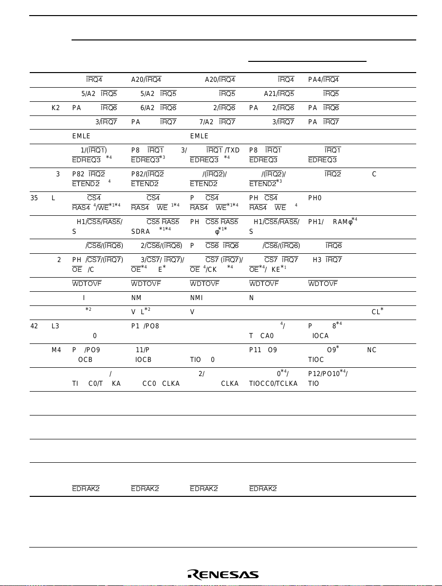
Section 1 Overview
Pin Name
Pin No.
LQFP
LGA
-144
-145 Mode 1
28 K4 A20/
IRQ4
29 J1 PA5/A21/
30 K2 PA6/A22/
31 J3 PA7/A23/
*
5
IRQ5
IRQ6
IRQ7
Mode 2
A20/
IRQ4
PA5/A21/
PA6/A22/
PA7/A23/
5
*
IRQ5
IRQ6
IRQ7
Mode 4 EXPE = 1 EXPE = 0
PA4/A20/
IRQ4
PA5/A21/
IRQ5
PA6/A22/
IRQ6
PA7/A23/
IRQ7
Mode 7
PA4/A20/
PA5/A21/
PA6/A22/
PA7/A23/
IRQ4
IRQ5
IRQ6
IRQ7
PA4/
PA5/
PA6/
PA7/
IRQ4
IRQ5
IRQ6
IRQ7
32 K1 EMLE EMLE EMLE EMLE EMLE
33 L2 P81/(
34 K3 P82/(
35 L1 PH0/
36 M1 PH1/
37 N2 PH2/
38 M2 PH3/
39 M3
IRQ1
)/TXD3/
P81/(
IRQ1
)/TXD3/
P81/(
IRQ1
)/TXD3/
P81/(
IRQ1
)/TXD3/
P81/(
EDREQ3
IRQ2
ETEND2
CS4
*
RAS4
CS5/RAS5
SDRAMφ
CS6/(IRQ6
CS7/(IRQ7
4
*
OE
/CKE
4
*3*
*3*
/
4
/
WE
*
1*4
EDREQ3
)/
P82/(
4
ETEND2
PH0/
4
*1*
RAS4
/
PH1/
SDRAMφ
)PH2/
)/
PH3/
4
1
*
*
OE
*3*
IRQ2
*3*
CS4
/
4
*
/
WE
CS5/RAS5
*
CS6/(IRQ6
CS7/(IRQ7
4
*
/CKE
1*4
*
4
)/
4
*1*
1
*
4
/
)PH2/
)/
4
EDREQ3
P82/(
IRQ2
ETEND2
PH0/
CS4
*
RAS4
PH1/
CS5/RAS5
SDRAMφ
CS6/(IRQ6
PH3/
CS7/(IRQ7
4
*
OE
/CKE
4
*3*
*3*
/
4
/
WE
*
1*4
EDREQ3
)/
P82/(
4
ETEND2
PH0/
4
*1*
RAS4
/
PH1/
SDRAMφ
)PH2/
)/
PH3/
4
1
*
*
OE
IRQ2
*3*
CS4
4
*
/
WE
CS5/RAS5
CS6/(IRQ6
CS7/(IRQ7
4
*
/CKE
*3*
/
*
4
)/
4
4
*1*
1*4
4
1
*
*
IRQ1
EDREQ3
P82/(
IRQ2
PH0 NC
/
PH1/SDRAMφ
)PH2/(
IRQ6
)/
PH3/(
IRQ7
WDTOVF WDTOVF WDTOVF WDTOVF WDTOVF
*3*
40 N1 NMI NMI NMI NMI NMI Vcc
2
41 N3 VCL
*
42 L3 P10/PO8
TIOCA0
43 M4 P11/PO9
TIOCB0
44 L4 P12/PO10
TIOCC0/TCLKA
45 N4 P13/PO11
TIOCD0/TCLKB
46 M5 P14/PO12
TIOCA1
47 L5 P15/PO13
TIOCB1/TCLKC
48 M6
P16/PO14
TIOCA2/
EDRAK2
4
*
/
4
*
/
4
*
/
4
*
/
4
*
/
4
*
/
4
*
/
3
*
2
*
VCL
4
*
P10/PO8
/
TIOCA0
P11/PO9
/
4
*
TIOCB0
4
P12/PO10
*
/
TIOCC0/TCLKA
4
P13/PO11
*
/
TIOCD0/TCLKB
4
P14/PO12
*
/
TIOCA1
4
P15/PO13
*
TIOCB1/TCLKC
4
P16/PO14
TIOCA2/
EDRAK2
*
/
3
*
2
*
VCL
4
*
P10/PO8
/
TIOCA0
P11/PO9
/
4
*
TIOCB0
4
P12/PO10
*
/
TIOCC0/TCLKA
4
P13/PO11
*
/
TIOCD0/TCLKB
4
P14/PO12
*
/
TIOCA1
4
P15/PO13
*
/
TIOCB1/TCLKC
4
P16/PO14
TIOCA2/
EDRAK2
*
/
3
*
2
*
VCL
4
*
P10/PO8
/
TIOCA0
P11/PO9
/
4
*
TIOCB0
4
P12/PO10
*
/
TIOCC0/TCLKA
4
P13/PO11
*
/
TIOCD0/TCLKB
4
P14/PO12
*
/
TIOCA1
4
P15/PO13
*
/
TIOCB1/TCLKC
4
P16/PO14
TIOCA2/
EDRAK2
*
/
3
*
2
*
VCL
*
P10/PO8
TIOCA0
*
P11/PO9
TIOCB0
P12/PO10
TIOCC0/TCLKA
P13/PO11
TIOCD0/TCLKB
P14/PO12
TIOCA1
P15/PO13
TIOCB1/TCLKC
P16/PO14
TIOCA2/
Flash Memory
Programmer
Mode
NC
NC
NC
NC
)/TXD3/
NC
4
)NC
4
*
NC
)NC
)NC
NC
VCL
4
/
NC
4
/
NC
4
*
/
NC
4
*
/
NC
4
*
/
NC
4
*
/
NC
4
*
NC
/
2
*
Rev. 5.00 Nov 18, 2005 page 15 of 1156
REJ09B0109-0500
Page 78
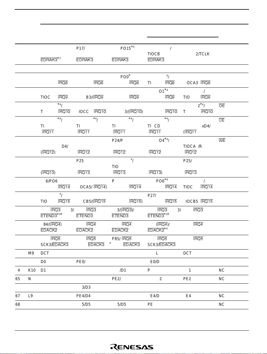
Section 1 Overview
Pin Name
Pin No.
4
*
/
3
Mode 7
4
P17/PO15
TIOCB2/TCLKD/
EDRAK3
*
/
3
*
P17/PO15
TIOCB2/TCLKD
LQFP
LGA
-144
-145 Mode 1
49 N5
5
*
4
P17/PO15
TIOCB2/TCLKD/
EDRAK3
*
/
3
*
5
*
Mode 2
P17/PO15
TIOCB2/TCLKD/
EDRAK3
4
*
/
3
*
Mode 4 EXPE = 1 EXPE = 0
P17/PO15
TIOCB2/TCLKD/
*
EDRAK3
50 K5 Vss Vss Vss Vss Vss Vss
51 L6
P20/PO0
TIOCA3/(
52 M7
P21/PO1
TIOCB3/(
53 N6
P22/PO2
TIOCC3/(
54 K6 P23/PO3
TIOCD3/TxD4/
IRQ11
(
55 K7
P24/PO4
TIOCA4/RxD4/
IRQ12
(
56 K8 P25/PO5
TIOCB4/
IRQ13
(
57 N7 P26/PO6
TIOCA5/(
58 M8 P27/PO7
TIOCB5/(
59 L7 P83/(
IRQ3
ETEND3
60 K9 P84/(
IRQ4
EDACK2
61 N8 P85/(
SCK3/
IRQ5
EDACK3
)
)
)
*3*
*
4
*
/
IRQ8
4
*
/
IRQ9
4
*
/
IRQ10
4
*
/
4
*
/
4
*
/
4
*
/
IRQ14
4
*
/
IRQ15
)/RxD3/
4
)/
4
)/
P20/PO0
TIOCA3/(
)
P21/PO1
)
TIOCB3/(
P22/PO2
)
TIOCC3/(
P23/PO3
TIOCD3/TxD4/
(
P24/PO4
TIOCA4/RxD4/
(
P25/PO5
TIOCB4/
(
P26/PO6
)
TIOCA5/(
P27/PO7
)
TIOCB5/(
P83/(
ETEND3
P84/(
EDACK2
P85/(
4
*3*
SCK3/
IRQ11
IRQ12
IRQ13
4
*
IRQ8
4
*
IRQ9
4
*
IRQ10
4
*
)
4
*
)
4
*
)
4
*
IRQ14
4
*
IRQ15
IRQ3
)/RxD3/
*3*
IRQ4
)/
4
*
IRQ5
)/
EDACK3
/
)
/
)
/
/
/
/
/
/
4
*3*
P20/PO0
TIOCA3/(
P21/PO1
TIOCB3/(
P22/PO2
)
TIOCC3/(
P23/PO3
TIOCD3/TxD4/
IRQ11
(
P24/PO4
TIOCA4/RxD4/
IRQ12
(
P25/PO5
TIOCB4/
IRQ13
(
P26/PO6
)
TIOCA5/(
P27/PO7
)
TIOCB5/(
P83/(
IRQ3
ETEND3
P84/(
IRQ4
EDACK2
P85/(
IRQ5
4
SCK3/
4
*
/
IRQ8
4
*
/
IRQ9
4
*
/
IRQ10
4
*
/
)
4
*
/
)
4
*
/
)
4
*
/
IRQ14
4
*
/
IRQ15
)/RxD3/
4
*3*
)/
4
*
)/
EDACK3
P20/PO0
TIOCA3/(
)
P21/PO1
)
TIOCB3/(
P22/PO2
)
TIOCC3/(
P23/PO3
TIOCD3/TxD4/
IRQ11
(
P24/PO4
TIOCA4/RxD4/
IRQ12
(
P25/PO5
TIOCB4/
IRQ13
(
P26/PO6
)
TIOCA5/(
P27/PO7
)
TIOCB5/(
P83/(
ETEND3
P84/(
EDACK2
P85/(
4
*3*
SCK3/
4
*
/
IRQ8
4
*
/
IRQ9
4
*
/
IRQ10
4
*
/
)
4
*
/
)
4
*
/
)
4
*
/
IRQ14
4
*
/
IRQ15
IRQ3
)/RxD3/
*3*
IRQ4
)/
4
*
IRQ5
)/
EDACK3
)
)
)
)
)
4
*3*
*
P20/PO0
TIOCA3/(
P21/PO1
TIOCB3/(
P22/PO2
TIOCC3/(
P23/PO3
IRQ8
*
IRQ9
*
IRQ10
*
TIOCD3/TxD4/
IRQ11
)
(
*
P24/PO4
TIOCA4/RxD4/
IRQ12
)
(
*
P25/PO5
TIOCB4/
IRQ13
)
(
*
P26/PO6
TIOCA5/(
P27/PO7
TIOCB5/(
P83/(
P84/(
P85/(
4
SCK3
IRQ14
*
IRQ15
IRQ3
IRQ4
IRQ5
62 M9 DCTL DCTL DCTL DCTL DCTL NC
63 L8 D0 PE0/D0 PE0/D0 PE0/D0 PE0 NC
64 K10 D1 PE1/D1 PE1/D1 PE1/D1 PE1 NC
65 N9 D2 PE2/D2 PE2/D2 PE2/D2 PE2 NC
66 M10 D3 PE3/D3 PE3/D3 PE3/D3 PE3 NC
67 L9 D4 PE4/D4 PE4/D4 PE4/D4 PE4 NC
68 N10 D5 PE5/D5 PE5/D5 PE5/D5 PE5 NC
Flash Memory
Programmer
Mode
4
*
NC
/
4
NC
/
)
4
NC
/
)
4
OE
/
)
4
/
CE
4
WE
/
4
/
Vss
4
NC
/
)
4
NC
/
)
)/RxD3 NC
)NC
)/
NC
Rev. 5.00 Nov 18, 2005 page 16 of 1156
REJ09B0109-0500
Page 79
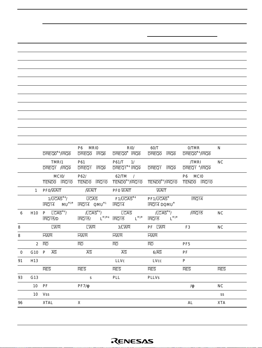
Section 1 Overview
Pin Name
Pin No.
LQFP
-144
LGA
-145 Mode 1
5
*
Mode 2
5
*
Mode 4 EXPE = 1 EXPE = 0
Mode 7
69 M11 D6 PE6/D6 PE6/D6 PE6/D6 PE6 NC
70 L10 Vss Vss Vss Vss Vss Vss
71 N11 D7 PE7/D7 PE7/D7 PE7/D7 PE7 NC
72 N12 Vcc Vcc Vcc Vcc Vcc Vcc
73M13D8D8D8D8PD0I/O0
74N13D9D9D9D9PD1I/O1
75 L12 D10 D10 D10 D10 PD2 I/O2
76 M12 D11 D11 D11 D11 PD3 I/O3
77 L11 D12 D12 D12 D12 PD4 I/O4
78 L13 D13 D13 D13 D13 PD5 I/O5
79 K12 D14 D14 D14 D14 PD6 I/O6
80 K11 D15 D15 D15 D15 PD7 I/O7
81 J12 P60/TMRI0/
82 K13 P61/TMRI1/
83 J10 P62/TMCI0/
84 J11 PF0/
85 H12 PF1/
86 H10 PF2/
87 J13 PF3/
88 H11
89 G12
90 G10 PF6/
4
*
DREQ0
4
*
DREQ1
4
*
TEND0
/
WAIT
UCAS
IRQ14
/DQMU
LCAS
IRQ15
/DQML
LWR
HWR HWR HWR HWR
RD RD RD RD
AS
/
/
IRQ8
IRQ9
IRQ10
4
*
/
4
*
/
*
1*4
*
1*4
P60/TMRI0/
4
*
DREQ0
P61/TMRI1/
4
*
DREQ1
P62/TMCI0/
4
*
TEND0
/
PF0/
WAIT
PF1/
UCAS
IRQ14
/DQMU
PF2/
LCAS
IRQ15
/DQML
PF3/
LWR
PF6/
AS
/
IRQ8
/
IRQ9
IRQ10
4
*
/
4
*
/
1*4
*
1*4
*
P60/TMRI0/
4
*
DREQ0
/
P61/TMRI1/
4
*
DREQ1
/
P62/TMCI0/
4
*
TEND0
/
PF0/
WAIT
PF1/
UCAS
IRQ14
/DQMU
PF2/
LCAS
IRQ15
/DQML
PF3/
LWR
PF6/
AS
IRQ8
IRQ9
IRQ10
4
*
/
4
*
/
*
1*4
*
1*4
P60/TMRI0/
4
*
DREQ0
P61/TMRI1/
4
*
DREQ1
P62/TMCI0/
4
*
TEND0
PF0/
WAIT
PF1/
UCAS
IRQ14
/DQMU
PF2/
LCAS
IRQ15
/DQML
PF3/
LWR
PF6/
AS
/
IRQ8
/
IRQ9
/
IRQ10
4
*
4
*
/
P60/TMRI0/
DREQ0
P61/TMRI1/
DREQ1
P62/TMCI0/
TEND0
PF0 NC
/
PF1/
IRQ14
1*4
*
PF2/
IRQ15
1*4
*
PF3 NC
PF4 NC
PF5 NC
PF6 NC
4
*
/
4
*
/
4
*
/
91 H13 PLLVcc PLLVcc PLLVcc PLLVcc PLLVcc Vcc
92 F12
RES RES RES RES RES RES
93 G13 PLLVss PLLVss PLLVss PLLVss PLLVss Vss
94 F10 PF7/φ PF7/φ PF7/φ PF7/φ PF7/φ NC
95 E10 Vss Vss Vss Vss Vss Vss
96 F13 XTAL XTAL XTAL XTAL XTAL XTAL
Flash Memory
Programmer
Mode
NC
IRQ8
NC
IRQ9
NC
IRQ10
NC
NC
Rev. 5.00 Nov 18, 2005 page 17 of 1156
REJ09B0109-0500
Page 80

Section 1 Overview
Pin Name
Pin No.
LQFP
-144
LGA
-145 Mode 1
5
*
Mode 2
5
*
Mode 4 EXPE = 1 EXPE = 0
Mode 7
97 E13 EXTAL EXTAL EXTAL EXTAL EXTAL EXTAL
98 F11 Vcc Vcc Vcc Vcc Vcc Vcc
99 D12 Vcc Vcc Vcc Vcc Vcc Vcc
100G11NCNCNCNCNCNC
101E12NCNCNCNCNCNC
102 E11 Vss Vss Vss Vss Vss Vss
103 D13
104 D10 P63/TMCI1/
105 C12 P64/TMO0/
106 C13 P65/TMO1/
107 D11 PG0/
108 B13 PG1/
109 A12
110 A13
STBY STBY STBY STBY STBY
TEND1
DACK0
DACK1
PG2/
RAS2
PG3/
RAS3
CS0
CS1
CS2
*
CS3
*
*
*
*
4
/
4
/
4
/I
RQ11
4
/
IRQ12
4
/
IRQ13
/
RAS
/
CAS
*
*1*
4
4
P63/TMCI1/
4
*
TEND1
/I
P64/TMO0/
4
*
DACK0
/
P65/TMO1/
4
*
DACK1
/
PG0/
CS0
PG1/
CS1
PG2/
CS2
/
4
*
RAS2
/
RAS
PG3/
CS3
/
4
*
RAS3
/
CAS
RQ11
IRQ12
IRQ13
*
*1*
4
4
P63/TMCI1/
4
*
TEND1
P64/TMO0/
4
*
DACK0
P65/TMO1/
4
*
DACK1
PG0/
CS0
PG1/
CS1
PG2/
CS2
4
*
RAS2
/
RAS
PG3/
CS3
4
*
RAS3
/
CAS
/I
RQ11
/
IRQ12
/
IRQ13
/
/
*
*1*
4
4
P63/TMCI1/
4
*
TEND1
/I
P64/TMO0/
4
*
DACK0
/
P65/TMO1/
4
*
DACK1
/
PG0/
CS0
PG1/
CS1
PG2/
CS2
4
*
RAS2
/
RAS
PG3/
CS3
4
*
RAS3
/
CAS
RQ11
IRQ12
IRQ13
/
*
/
*1*
P63/TMCI1/
TEND1
P64/TMO0/
DACK0
P65/TMO1/
DACK1
PG0 NC
PG1 NC
PG2 NC
4
PG3 NC
4
4
*
/I
4
*
/
4
*
/
111 B11 AVcc AVcc AVcc AVcc AVcc Vcc
112 B12 Vref Vref Vref Vref Vref NC
113 A11 P40/AN0 P40/AN0 P40/AN0 P40/AN0 P40/AN0 NC
114 C11 P41/AN1 P41/AN1 P41/AN1 P41/AN1 P41/AN1 NC
115 B10 P42/AN2 P42/AN2 P42/AN2 P42/AN2 P42/AN2 NC
116 C10 P43/AN3 P43/AN3 P43/AN3 P43/AN3 P43/AN3 NC
117 A10 P44/AN4 P44/AN4 P44/AN4 P44/AN4 P44/AN4 NC
118 B9 P45/AN5 P45/AN5 P45/AN5 P45/AN5 P45/AN5 NC
119 C9 P46/AN6/DA0
120 B8 P47/AN7/DA1
3
*
P46/AN6/DA0
3
*
P47/AN7/DA1
3
*
P46/AN6/DA0
3
*
P47/AN7/DA1
3
*
P46/AN6/DA0
3
*
P47/AN7/DA1
3
*
P46/AN6/DA0
3
*
P47/AN7/DA1
121 A9 P90/AN8 P90/AN8 P90/AN8 P90/AN8 P90/AN8 NC
122 D9 P91/AN9 P91/AN9 P91/AN9 P91/AN9 P91/AN9 NC
123 C8 P92/AN10 P92/AN10 P92/AN10 P92/AN10 P92/AN10 NC
124 B7 P93/AN11 P93/AN11 P93/AN11 P93/AN11 P93/AN11 NC
RQ11
IRQ12
IRQ13
*
*
Flash Memory
Programmer
Mode
Vcc
NC
NC
NC
3
NC
3
NC
Rev. 5.00 Nov 18, 2005 page 18 of 1156
REJ09B0109-0500
Page 81

Section 1 Overview
Pin Name
Pin No.
LQFP
-144
LGA
-145 Mode 1
5
*
Mode 2
5
*
Mode 4 EXPE = 1 EXPE = 0
Mode 7
Flash Memory
Programmer
Mode
125 A8 P94/AN12/DA2 P94/AN12/DA2 P94/AN12/DA2 P94/AN12/DA2 P94/AN12/DA2 NC
126 D8 P95/AN13/DA3 P95/AN13/DA3 P95/AN13/DA3 P95/AN13/DA3 P95/AN13/DA3 NC
127 D7 P96/AN14/DA4
128 D6 P97/AN15/DA5
3*4
*
P96/AN14/DA4
3*4
*
P97/AN15/DA5
3*4
*
P96/AN14/DA4
3*4
*
P97/AN15/DA5
3*4
*
P96/AN14/DA4
3*4
*
P97/AN15/DA5
3*4
*
P96/AN14/DA4
3*4
*
P97/AN15/DA5
3*4
*
NC
3*4
*
NC
129 A7 AVss AVss AVss AVss AVss Vss
130 B6 PG4/
131 C7 PG5/
132 D5 PG6/
133 A6 P50/TxD2/
134 B5 P51/RxD2/
135 C6 P52/SCK2/
136 D4 P53/
137 A5
138 B4
BREQO
BACK
BREQ
IRQ0
IRQ1
IRQ2
ADTRG
/
IRQ3
P35/SCK1/SCL0/
4
/(CKE)
1
*
*
OE
)
(
P34/SCK0/
SCK4/SDA0
PG4/
BREQO
PG5/
BACK
PG6/
BREQ
P50/TxD2/
P51/RxD2/
P52/SCK2/
P53/
ADTRG
IRQ3
P35/SCK1/SCL0/
4
4
*
*
OE
)
(
P34/SCK0/
SCK4/SDA0
IRQ0
IRQ1
/(CKE)
IRQ2
/
*
4
1
*
PG4/
BREQO
PG5/
BACK
PG6/
BREQ
P50/TxD2/
P51/RxD2/
P52/SCK2/
P53/
ADTRG
IRQ0
IRQ1
IRQ2
/
IRQ3
P35/SCK1/SCL0/
4
1
*
)
/(CKE)
*
(
OE
P34/SCK0/
SCK4/SDA0
PG4/
BREQO
PG5/
BACK
PG6/
BREQ
P50/TxD2/
P51/RxD2/
P52/SCK2/
P53/
ADTRG
IRQ3
P35/SCK1/SCL0/
4
4
*
*
OE
)
(
P34/SCK0/
SCK4/SDA0
IRQ0
IRQ1
/(CKE)
PG4 NC
PG5 NC
PG6 NC
P50/TxD2/
P51/RxD2/
IRQ2
P52/SCK2/
/
P53/
IRQ3
P35/SCK1/SCL0 NC
4
1
*
*
P34/SCK0/
SCK4/SDA0
ADTRG
IRQ0
IRQ1
IRQ2
/
Vss
Vss
Vcc
NC
NC
139 C5 P33/RxD1/SCL1 P33/RxD1/SCL1 P33/RxD1/SCL1 P33/RxD1/SCL1 P33/RxD1/SCL1 NC
140 A4 P32/RxD0/
IrRxD/SDA1
P32/RxD0/
IrRxD/SDA1
P32/RxD0/
IrRxD/SDA1
P32/RxD0/
IrRxD/SDA1
P32/RxD0/
IrRxD/SDA1
Vcc
141 B3 P31/TxD1 P31/TxD1 P31/TxD1 P31/TxD1 P31/TxD1 NC
142 C4 P30/TxD0/IrTxD P30/TxD0/IrTxD P30/TxD0/IrTxD P30/TxD0/IrTxD P30/TxD0/IrTxD NC
143 A3 MD0 MD0 MD0 MD0 MD0 Vss
144 A2 MD1 MD1 MD1 MD1 MD1 Vss
145 E5 NC NC NC NC NC NC
Notes: 1. Not available for the H8S/2378 Group.
2. These pins are Vcc pins in the H8S/2377, H8S/2377R, H8S/2376, H8S/2375,
H8S/2375R, H8S/2373, and H8S/2373R.
3. Not available for the H8S/2375 and H8S/2375R.
4. Not available for the H8S/2376.
5. Only modes 1 and 2 may be used on ROM-less versions.
Rev. 5.00 Nov 18, 2005 page 19 of 1156
REJ09B0109-0500
Page 82

Section 1 Overview
1.3.3 Pin Functions
Table 1.2 Pin Functions
H8S/2378
H8S/2377R
Type Symbol
Power V
CC
V
SS
PLLV
PLLV
VCL
(LQFP
-144)
4, 41, 72,
98, 99
2, 10, 18,
25, 50, 70,
95, 102
91 H13 91 91 91 Input Power supply pin for
CC
93 G13 93 93 93 Input Ground pin for the
SS
3
*
41 N3 Output
H8S/2378
(LGA-145)
B2, N12,
F11, D12
A1, E2,
F4, H1,
K5, L10,
E10, E11
Pin No.
H8S/2377
H8S/2377R
4, 41, 72,
98, 99
2, 10, 18,
25, 50, 70,
95, 102
H8S/23 76
4, 41,
72, 98,
99
2, 10,
18,
25, 50,
70,
95, 102
H8S/2375
H8S/2373
H8S/2375R
H8S/2373R
4, 41, 72,
98, 99
2, 10, 18,
25, 50, 70,
95, 102
I/O Function
Input For connection to
the power supply.
pins should be
V
CC
connec te d t o the
system power
supply.
Input For connection to
ground . V
SS
pins
should be
connec te d t o the
system power
supply (0 V).
the on-chi p PLL
oscillator.
on-chip PL L
oscillator.
This pin must not be
connec te d t o the
system power
supply and should
be connected V
pin via 0.1-µF
(recommended
value)
capacitor (place it
close to pin).
SS
Rev. 5.00 Nov 18, 2005 page 20 of 1156
REJ09B0109-0500
Page 83

Section 1 Overview
Pin No.
H8S/2378
H8S/2377R
Type Symbol
Clock XTAL 96 F13 96 96 96 Input For connection to a
EXTAL 97 E13 97 97 97 Input For connection to a
φ 94 F10 94 94 94 Output Supplies the system
SDRAMφ
1*4
*
(LQFP
-144)
36 M1 36 36 Output
H8S/2378
(LGA-145)
H8S/2377
H8S/2377R
H8S/23 76
H8S/2375
H8S/2373
H8S/2375R
H8S/2373R
I/O Function
crystal oscillator.
See section 23,
Clock Pulse
Generator, for
typical connection
diagrams for a
crystal resonator
and external cloc k
input.
crystal oscillator.
The EXTAL pin can
also input an
external c l ock. See
section 23, Clock
Pulse Generator, for
typical connection
diagrams for a
crystal resonator
and external cloc k
input.
clock to external
devices.
When a synchronous DRAM is
connected, this pin
is connected to the
CLK pin of the
synchronous
DRAM. For details,
refer to section 6,
Bus Controller
(BSC).
Rev. 5.00 Nov 18, 2005 page 21 of 1156
REJ09B0109-0500
Page 84

Section 1 Overview
Type Symbol
Operating
mode
control
System
control
MD2
MD1
MD0
DCTL
RES
STBY
1
*
Pin No.
H8S/2378
H8S/2377R
(LQFP
-144)
1, 144,
143
62 M9 62 62 62 Input
92 F12 92 92 92 Input
103 D13 103 103 103 Input When this pin is
H8S/2378
(LGA-145)
B1, A2, A3 1, 144,
H8S/2377
H8S/2377R
143
H8S/23 76
1, 144,
143
H8S/2375
H8S/2373
H8S/2375R
H8S/2373R
1, 144,
143
I/O Function
Input These pins set the
operating mode.
These pins should
not be chan ged
while the MCU is
operating.
When this pin is
driven high for the
H8S/2378R Group,
SDRAMφ dedicated
to the synchron ous
DRAM is output.
When not using the
synchronous DRAM
interface or for th e
H8S/2378 Group,
drive this pin low.
The level of this pin
must not be
change d during
operation.
Reset pin. When
this pin is driven
low, the chip is
reset.
driven low, a
transition is made to
hardware standby
mode.
Rev. 5.00 Nov 18, 2005 page 22 of 1156
REJ09B0109-0500
Page 85

Type Symbol
System
control
EMLE 32 K1 32 32 32 Input On-chip Emulator
H8S/2378
H8S/2377R
(LQFP
-144)
H8S/2378
(LGA-145)
Pin No.
H8S/2377
H8S/2377R
H8S/23 76
H8S/2375
H8S/2373
H8S/2375R
H8S/2373R
Section 1 Overview
I/O Function
Enable Pin
When the on-chip
emulator in the
H8S/2378,
H8S/2377,
H8S/2377R, or
H8S/2378R is used,
this pin shoul d be
fixed hig h . At thi s
time, pins P53, PG4
to PG6, and
WDTOVF
exclusively for the
on-chip emulator ,
therefore, the
corresponding pin
functions of thos e
pins are n ot
available.
When the on-chip
emulator is not used
or the H8S/2375,
H8S/2376,
H8S/2375R,
H8S/2373, or
H8S/2373R is used,
this pin shoul d be
fixed low.
For details, refer to
E10A Em ulator
User’s Manual.
are
Rev. 5.00 Nov 18, 2005 page 23 of 1156
REJ09B0109-0500
Page 86

Section 1 Overview
H8S/2378
H8S/2377R
Type Symbol
Address
bus
Data bus D15 to D0 80 to 73,
Bus control
A23 to A0 31 to 26,
CS7
CS0
AS
RD
(LQFP
-144)
24 to 19,
17 to 11,
9 to 5
71,
69 to 63
to
38 to 35,
110 to 107
90 G10 90 90 90 Output
89 G12 89 89 89 Output When this pin is low,
H8S/2378
(LGA-145)
J3, K2, J1,
K4, H3,
J2, J4, G3,
H2, G1,
H4, G4,
F1, G2,
F3, E4,
E1, F2,
E3, D1,
D3, D2,
C3, C1
K11, K12,
L13, L11,
M12, L12,
N13, M13,
N11, M11,
N10, L9,
M10, N9,
K10, L8
M2, N2,
M1, L1,
A13, A12,
B13, D11
Pin No.
H8S/2377
H8S/2377R
31 to 26,
24 to 19,
17 to 11,
9 to 5
80 to 73,
71,
69 to 63
38 to 35,
110 to 107
H8S/23 76
31 to 26,
24 to 19,
17 to 11,
9 to 5
80 to 73,
71,
69 to 63
38 to 35,
110 to
107
H8S/2375
H8S/2373
H8S/2375R
H8S/2373R
31 to 26,
24 to 19,
17 to 11,
9 to 5
80 to 73,
71,
69 to 63
38 to 35,
110 to 107
I/O Function
Output These pins output
an address.
Input/
These pins
output
constitute a
bidirect ional data
bus.
Output Signals that select
division areas 7 to 0
in the external
address sp ace
When this pin is low,
it indicates that
address o utput on
the address bus is
valid.
it indicates that the
external a ddress
space is being read.
Rev. 5.00 Nov 18, 2005 page 24 of 1156
REJ09B0109-0500
Page 87

Type Symbol
Bus control
HWR
LWR
BREQ
BREQO
BACK
Section 1 Overview
Pin No.
H8S/2378
H8S/2377R
(LQFP
-144)
88 H11 88 88 88 Output Strobe signal
87 J13 87 87 87 Output Strobe signal
132 D5 132 132 132 Input The external b us
130 B6 130 130 130 Output
131 C7 131 131 131 Output Indicates the bus is
H8S/2378
(LGA-145)
H8S/2377
H8S/2377R
H8S/23 76
H8S/2375
H8S/2373
H8S/2375R
H8S/2373R
I/O Function
indicating that
external a ddress
space is to be
written, and the
upper half (D15 to
D8) of the d at a bus
is enabled.
Write enable signal
for a ccessing the
DRAM space.
indicating that
external a ddress
space is to be
written, and the
lower half (D7 to
D0) of the d at a bus
is enabled.
master requests the
bus to this LSI.
External bus
request signa l whe n
the internal bus
master ac c es ses
the external spac e
in extern al b us
release state.
released to the
external bus master.
Rev. 5.00 Nov 18, 2005 page 25 of 1156
REJ09B0109-0500
Page 88

Section 1 Overview
Type Symbol
4
Bus control
UCAS
LCAS
DQMU
DQML
*
*
4
*1*
*1*
Pin No.
H8S/2378
H8S/2377R
(LQFP
-144)
H8S/2378
(LGA-145)
H8S/2377
H8S/2377R
H8S/23 76
H8S/2375
H8S/2373
H8S/2375R
H8S/2373R
I/O Function
85 H12 85 85 Output Upper column
address strobe
signal for accessing
the 16-bit DRAM
space.
Column address
strobe signal for
accessing the 8-bit
DRAM space.
86 H10 86 86 Output Lower col umn
address strobe
signal for accessing
the 16-bit DRAM
space.
4
85 H12 85 85 Output Upper data mask
enable signal for 16bit synchron ous
DRAM for accessing
the 16-bit
synchronous DRAM
space.
Data mask enable
signal for accessing
the 8-bi t
synchronous DRAM
space.
4
86 H10 86 86 Output
Lower-data mask
enable signal for
accessing the 16-bit
synchronous DRAM
interface space.
Rev. 5.00 Nov 18, 2005 page 26 of 1156
REJ09B0109-0500
Page 89

Type Symbol
4
Bus control
RAS
RAS2
RAS3
RAS5
RAS
CAS
*1*
WE
*
*
*
*
*1*
*1*
WAIT
Section 1 Overview
Pin No.
H8S/2378
H8S/2377R
(LQFP
-144)
/
109, 110,
4
35, 36
4
to
4
4
109 A12 109 109 Output Row address strobe
4
110 A13 110 110 Outp ut Column address
4
35 L1 35 35 Output Write enable signal
H8S/2378
(LGA-145)
A12,
A13,
L1,
M1
H8S/2377
H8S/2377R
109, 110,
35, 36
H8S/23 76
109, 110,
84 J11 84 84 84 Input Requests insertion
H8S/2375
H8S/2373
H8S/2375R
H8S/2373R
35, 36
I/O Function
Output Row address strobe
signal for the
synchronous DRAM
interface.
RAS
signal is a row
address strobe
signal when areas 2
to 5 are set to the
continuous DRAM
space.
signal for the
synchronous DRAM
of the synchronous
DRAM interface.
strobe signal for the
synchronous DRAM
of the synchronous
DRAM interface.
for the synch ronous
DRAM of the
synchronous DRAM
interface.
of a wait state in the
bus cycle when
accessing exter n al
3-stat e a ddress
space.
Rev. 5.00 Nov 18, 2005 page 27 of 1156
REJ09B0109-0500
Page 90

Section 1 Overview
Type Symbol
4
Bus control
Interrupt
signals
*
OE
4
*
(OE)
1*4
*
CKE
*1*
(CKE)
NMI 40 N1 40 40 40 Input
IRQ15
to
IRQ0
(
IRQ15
) to
IRQ0
)
(
H8S/2378
H8S/2377R
(LQFP
-144)
38,
137
38,
4
137
86, 85,
106 to
104,
83 to 81,
31 to 28,
136 to 133
58 to 51,
38, 37,
61 to 59,
34, 33, 3
H8S/2378
(LGA-145)
M2,
A5
M2,
A5
H10, H12,
C13, C12,
D10, J10,
K13, J12,
J3, K2, J1,
K4, D4,
C6, B5, A6
M8, N7,
K8, K7,
K6, N6,
M7, L6,
M2, N2,
N8, K9,
L7, K3, L2,
C2
Pin No.
H8S/2377
H8S/2377R
38,
137
38,
137
86, 85,
106 to
104,
83 to 81,
31 to 28,
136 to 133
58 to 51,
38, 37,
61 to 59,
34, 33, 3
H8S/2375
H8S/2373
H8S/2375R
H8S/23 76
H8S/2373R
38,
137
38,
137
86, 85,
106 to
104,
83 to 81,
31 to 28,
86, 85,
106 to 104,
83 to 81,
31 to 28,
136 to 133
136 to
133
58 to 51,
38, 37,
61 to 59,
34, 33, 3
58 to 51,
38, 37,
61 to 59,
34, 33, 3
I/O Function
Output Output enable
signal for DRAM
interface space.
The output pins of
OE
and (OE) are
selected by the port
function control
register 2 (PFCR2)
of port 3.
Output Clock enable signal
of the synchronous
DRAM interface
space.
The output pins of
CKE
CKE and (
) are
selected by the port
function control
register 2 (PFCR2)
of port 3.
Nonmaskable
interrupt request
pin. Fix high when
not used.
These pins request
Input
a maskable
interrupt.
The input pins of
IRQn
and (
IRQn
)
are selected by the
IRQ pin select
register (ITSR) of
the interrupt
controller.
(n = 0 to 15)
Rev. 5.00 Nov 18, 2005 page 28 of 1156
REJ09B0109-0500
Page 91

Type Symbol
DMA
controller
(DMAC)
*
4
DREQ1
DREQ0
TEND1
TEND0
DACK1
DACK0
EXDMA
controller
(EXDMAC)
2*4
*
EDREQ3,
EDREQ2
ETEND3,
ETEND2
EDACK3,
EDACK2
EDRAK3,
EDRAK2
16-bit timer
pulse unit
(TPU)
TCLKA
TCLKB
TCLKC
TCLKD
TIOCA0
TIOCB0
TIOCC0
TIOCD0
H8S/2378
H8S/2377R
(LQFP
-144)
82,
81
104,
83
106,
105
33,
3
59,
34
61,
60
49,
48
44,
45,
47,
49
42,
43,
44,
45
H8S/2378
(LGA-145)
K13,
J12
D10,
J10
C13,
C12
L2,
C2
L7,
K3
N8,
K9
N5,
M6
L4,
N4,
L5,
N5
L3,
M4,
L4,
N4
Pin No.
H8S/2377
H8S/2377R H8S/2376
82,
82,
81
104,
104,
83
106,
106,
105
33,
Input These signals
3
59,
Output These signals
34
61,
Output EXDMAC single
60
49,
Output These signals notify
48
44,
45,
47,
49
42,
43,
44,
45
44,
45,
47,
49
42,
43,
44,
45
Section 1 Overview
H8S/2375
H8S/2373
H8S/2375R
H8S/2373R I/O Function
Input These signals
81
83
105
44,
45,
47,
49
42,
43,
44,
45
request DMAC
activation.
Output These signals
indicate the end of
DMAC data transfer.
Output DMAC single
address transfer
acknowledge
signals.
request EXDMAC
activation.
indicate the end of
EXDMAC data
transfer.
address transfer
acknowledge
signals.
an external device
of acceptance and
start of execution of
a DMA transfer
request.
Input External clock input
pins of the timer.
Input/
TGRA_0 to
output
TGRD_0 input
capture input/output
compare output/
PWM output pins.
Rev. 5.00 Nov 18, 2005 page 29 of 1156
REJ09B0109-0500
Page 92

Section 1 Overview
Type Symbol
16-bit timer
pulse unit
(TPU)
Programmable
pulse
generator
(PPG)
8-bit timer
(TMR)
*
TIOCA1
TIOCB1
TIOCA2
TIOCB2
TIOCA3
TIOCB3
TIOCC3
TIOCD3
TIOCA4
TIOCB4
TIOCA5,
TIOCB5
PO15 to
PO0
4
TMO0
TMO1
TMCI0
TMCI1
TMRI0
TMRI1
H8S/2378
H8S/2377R
(LQFP
-144)
46,
47
48,
49
51,
52,
53,
54
55,
56
57,
58
49 to 42,
58 to 51
105,
106
83,
104
82,
81
H8S/2378
(LGA-145)
M5,
L5
M6,
N5
L6,
M7,
N6,
K6
K7,
K8
N7,
M8
N5, M6,
L5, M5,
N4, L4,
M4, L3,
M8, N7,
K8, K7,
K6, N6,
M7, L6
C12,
C13
J10,
D10
K13,
J12
Pin No.
H8S/2377
H8S/2377R H8S/2376
46,
47
48,
49
51,
52,
53,
54
55,
56
57,
58
49 to 42,
46,
47
48,
49
51,
52,
53,
54
55,
56
57,
58
58 to 51
105,
106
83,
104
82,
81
105,
106
83,
104
82,
81
H8S/2375
H8S/2373
H8S/2375R
H8S/2373R I/O Function
46,
47
Input/
output
TGRA_1 and
TGRB_1 input
capture input/output
compare output/
PWM output pins.
48,
49
Input/
output
TGRA_2 and
TGRB_2 input
capture input/output
compare output/
PWM output pins.
Input/
51,
52,
53,
54
TGRA_3 to
output
TGRD_3 input
capture input/output
compare output/
PWM output pins.
55,
56
Input/
output
TGRA_4 and
TGRB_4 input
capture input/output
compare output/
PWM output pins.
57,
58
Input/
output
TGRA_5 and
TGRB_5 input
capture input/output
compare output/
PWM output pins.
49 to 42,
Output Pulse output pins.
58 to 51
105,
106
Output Waveform output
pins with output
compare function.
83,
104
82,
81
Input External event input
pins.
Input Counter reset input
pins.
Rev. 5.00 Nov 18, 2005 page 30 of 1156
REJ09B0109-0500
Page 93
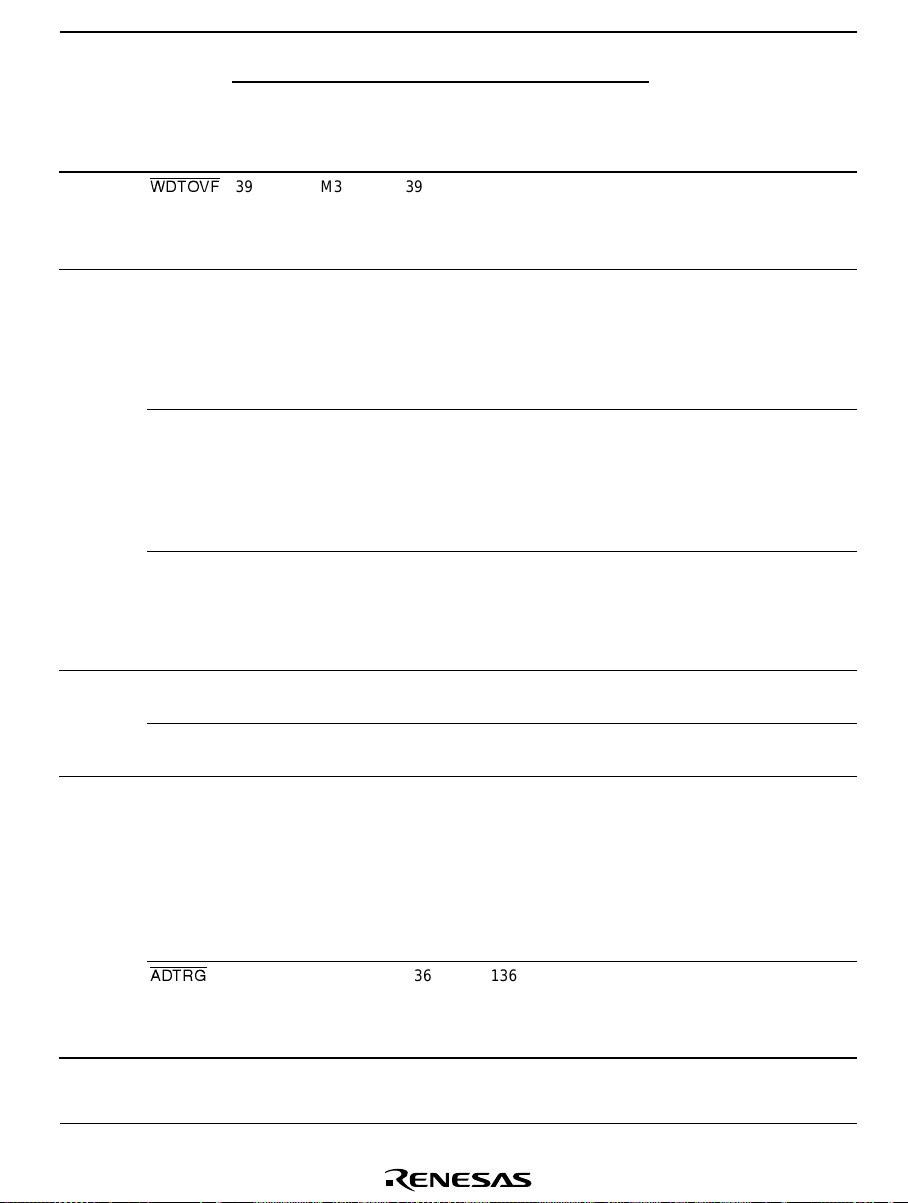
Type Symbol
Watchdog
timer
(WDT)
Serial
communication
interface
(SCI)/smart
card
interface
(SCI_0
with IrDA
function)
I2C bus
interface 2
(IIC2)
A/D
converter
WDTOVF
TxD4
TxD3
TxD2
TxD1
TxD0/
IrTxD
RxD4
RxD3
RxD2
RxD1
RxD0/
IrRxD
SCK4
SCK3
SCK2
SCK1
SCK0
SCL1
SCL0
SDA1
SDA0
AN15 to
AN0
ADTRG
Section 1 Overview
Pin No.
H8S/2378
H8S/2377R
(LQFP
-144)
39 M 3 39 39 39 Outp ut Coun ter overflow
54,
33,
133,
141,
142
55,
59,
134,
139,
140
138,
61,
135,
137,
138
139,
137
140,
138
128 to 113
136 D4 136 136 136 Input
H8S/2378
(LGA-145)
K6,
L2,
A6,
B3,
C4
K7,
L7,
B5,
C5,
A4
B4,
N8,
C6,
A5,
B4
C5,
A5
A4,
B4
D6, D7,
D8, A8,
B7, C8,
D9, A9,
B8, C9,
B9, A10,
C10, B10,
C11, A11
H8S/2377
H8S/2377R
54,
33,
133,
141,
142
55,
59,
134,
139,
140
138,
61,
135,
137,
138
139,
137
140,
138
128 to 113
H8S/23 76
54,
33,
133,
141,
142
55,
59,
134,
139,
140
138,
61,
135,
137,
138
139,
137
140,
138
128 to
113
H8S/2375
H8S/2373
H8S/2375R
H8S/2373R
54,
33,
133,
141,
142
55,
59,
134,
139,
140
138,
61,
135,
137,
138
139,
137
140,
138
128 to 113 Input
I/O Function
Output Data output pins.
Input Data input pins.
Input/
output
Input/
output
Input/
output
signal output pin in
watchdog time r
mode.
Clock input /output
pins.
I2C clock input/
output pin s.
2
C data input/ output
I
pins.
Analog input pins for
the A/D converter .
Pin for input of an
external tr i gger to
start A/D
conversion.
Rev. 5.00 Nov 18, 2005 page 31 of 1156
REJ09B0109-0500
Page 94

Section 1 Overview
Type Symbol
4
*
DA5
converter
A/D
converter,
D/A
converter
4
*
DA4
DA3 126 D8 126 126 126
DA2 125 A8 125 125 125
DA1 120 B8 120
DA0 119 C9 119
AV
CC
AV
SS
Vref 112 B12 112 112 112 Input The reference
Pin No.
H8S/2378
H8S/2377R
(LQFP
-144)
H8S/2378
(LGA-145)
H8S/2377
H8S/2377R H8S/2376
128 D6 OutputD/A
127 D7
H8S/2375
H8S/2373
H8S/2375R
H8S/2373R I/O Function
Analog output pins
for the D/A
converter.
111 B11 111 111 111 Input The analog power-
supply pin for the
A/D converter and
D/A converter.
When the A/D
converter and D/A
converter are not
used, this pin should
be connected to the
system power
supply (+3 V).
129 A7 129 129 129 Input The ground pin for
the A/D converter
and D/A converter.
This pin should be
connected to the
system power
supply (0 V).
voltage input pin for
the A/D converter
and D/A converter.
When the A/D
converter and D/A
converter are not
used, this pin should
be connected to the
system power
supply (+3 V).
Rev. 5.00 Nov 18, 2005 page 32 of 1156
REJ09B0109-0500
Page 95

Type Symbol
I/O ports P17 to
P10
P27 to
P20
P35 to
P30
P47 to
P40
P53 to
P50
P65 to
P60
P85 to
P80
P97 to
P90
PA7 to
PA0
PB7 to
PB0
PC7 to
PC0
H8S/2378
H8S/2377R
(LQFP
-144)
49 to 42 N5, M6,
58 to 51 M8, N7,
137 to 142 A5, B4,
120 to 113 B8, C9,
136 to 133
106 to
104,
83 to 81
61 to 59,
34, 33, 3
128 to 121
31 to 26,
24, 23
22 to 19,
17 to 14
13 to 11,
9 to 5
H8S/2378
(LGA-145)
L5, M5,
N4, L4,
M4, L3
K8, K7,
K6, N6,
M7, L6
C5, A4,
B3, C4
B9, A10,
C10, B10,
C11, A11
D4, C6,
B5, A6
C13, C12,
D10, J10,
K13, J12
N8, K9,
L7, K3, L2,
C2
D6, D7,
D8, A8,
B7, C8,
D9, A9
J3, K2, J1,
K4, H3,
J2, J4, G3
H2, G1,
H4, G4,
F1, G2,
F3, E4
E1, F2,
E3, D1,
D3, D2,
C3, C1
Pin No.
H8S/2375
H8S/2373
H8S/2377
H8S/2377R
49 to 42 49 to 42 49 to 42 Input/
58 to 51 58 to 51 58 to 51 Input/
137 to 142 137 to
120 to 113 120 to
136 to 133
106 to
104,
83 to 81
61 to 59,
34, 33, 3
128 to 121
31 to 26,
24, 23
22 to 19,
17 to 14
13 to 11,
9 to 5
H8S/23 76
142
113
136 to
133
106 to
104,
83 to 81
61 to 59,
34, 33, 3
128 to
121
31 to 26,
24, 23
22 to 19,
17 to 14
13 to 11,
9 to 5
H8S/2375R
H8S/2373R
137 to 142 Input/
120 to 113 Input Eight-bit input pins.
136 to 133
106 to 104,
83 to 81
61 to 59,
34, 33, 3
128 to 121 Input Eight-bit input pins.
31 to 26,
24, 23
22 to 19,
17 to 14
13 to 11,
9 to 5
I/O Function
output
output
output
Input/
output
Input/
output
Input/
output
Input/
output
Input/
output
Input/
output
Section 1 Overview
Eight-bit input/
output pin s.
Eight-bit input/
output pin s.
Six-bit input/output
pins.
Four-bit input/output
pins.
Six-bit input/output
pins.
Six-bit input/output
pins.
Eight-bit input/
output pin s.
Eight-bit input/
output pin s.
Eight-bit input/
output pin s.
Rev. 5.00 Nov 18, 2005 page 33 of 1156
REJ09B0109-0500
Page 96

Section 1 Overview
Pin No.
H8S/2378
H8S/2377R
Type Symbol
I/O ports PD7 to
PD0
PE7 to
PE0
PF7 to
PF0
PG6 to
PG0
PH3 to
PH0
(LQFP
-144)
80 to 73 K11, K12,
71,
69 to 63
94,
90 to 84
132 to
130,
110 to 107
38 to 35
H8S/2378
(LGA-145)
L13, L11,
M12, L12,
N13, M13
N11, M11,
N10, L9,
M10, N9,
K10, L8
F10, G10,
G12, H11,
J13, H10,
H12, J11
D5, C7,
B6, A13,
A12, B13,
D11
M2, N2,
M1, L1
H8S/2377
H8S/2377R
80 to 73 80 to 73 80 to 73 Input/
71,
69 to 63
94,
90 to 84
132 to
130,
110 to 107
38 to 35 38 to 35 38 to 35
Notes: 1. Not available for the H8S/2378 Group.
2. Not available for the H8S/2375, H8S/2375R, H8S/2373, and H8S/2373R.
3. Available only for the H8S/2378 and H8S/2378R.
4. Not available for the H8S/2376.
H8S/23 76
71,
69 to 63
94,
90 to 84
132 to
130,
110 to
107
H8S/2375
H8S/2373
H8S/2375R
H8S/2373R
71,
69 to 63
94,
90 to 84
132 to 130,
110 to 107
I/O Function
Eight-bit input/
output
output pin s.
Input/
Eight-bit input/
output
output pin s.
Input/
Eight-bit input/
output
output pin s.
Input/
Seven-bit input/
output
output pin s.
Input/
Four-bit input/output
output
pins.
Rev. 5.00 Nov 18, 2005 page 34 of 1156
REJ09B0109-0500
Page 97

Section 2 CPU
Section 2 CPU
The H8S/2000 CPU is a high-speed central processing unit with an internal 32-bit architecture that
is upward-compatible with the H8/300 and H8/300H CPUs. The H8S/2000 CPU has sixteen 16-bit
general registers, can address a 16-Mbyte linear address space, and is ideal for realtime control.
This section describes the H8S/2000 CPU. The usable modes and address spaces differ depending
on the product. For details on each product, refer to section 3, MCU Operating Modes.
2.1 Features
• Upward-comp at ib ilit y with H8/300 and H8/300H CPUs
Can execute H8/300 and H8/300H CPU object programs
• General-reg i ster arch ite ctu re
Sixteen 16-bit general registers also usable as sixteen 8-bit registers or eight 32-bit registers
• Sixty-five basic instructions
8/16/32-bit arithm etic and log i c instruc tions
Multiply and divide instructions
Powerful bit-manipulation instructions
• Eight addressing modes
Register direct [Rn]
Register indirect [@ERn]
Register indirect with displacement [@(d:16,ERn) or @(d:32,ERn)]
Register indirect with post-increment or pre-decrement [@ERn+ or @–ERn]
Absol ute address [@aa: 8, @a a:16, @aa:24, or @aa:32]
Immediate [#xx:8, #xx:16, or #xx:32]
Program-counter relative [@(d:8,PC) or @(d:16,PC)]
Memory indirect [@@aa:8]
• 16-Mbyte address space
Program: 16 Mbytes
Data: 16 Mbytes
• High-speed operation
All frequently-used instructions are executed in one or two states
8/16/32-bit register-register add/subtract: 1 state
8 × 8-bit register-register multiply: 12 states (MULXU.B), 13 states (MULXS.B)
16 ÷ 8-bit register-register divide: 12 states (DIVXU.B)
CPUS211A_000020020400
Rev. 5.00 Nov 18, 2005 page 35 of 1156
REJ09B0109-0500
Page 98

Section 2 CPU
16 × 16-bit register-register multiply: 20 states (MULXU.W), 21 states (MULXS.W)
32 ÷ 16-bit register-register divide: 20 states (DIVXU.W)
• Two CPU operating modes
Normal mode
*
Advanced mode
Note: * For this LSI, normal mode is not available.
• Power-down state
Transition to power-down state by SLEEP instruction
Selectable CPU clock speed
2.1.1 Differences between H8S/2600 CPU and H8S/2000 CPU
The differences between the H8S/2600 CPU and the H8S/2000 CPU are as shown below.
• Register configuration
The MAC register is supported only by the H8S/2600 CPU.
• Basic instructions
The four instructions MAC, CLRMAC, LDMAC, and STMAC are supported only by the
H8S/2600 CPU.
• The number of execution states of the MULXU and MULXS instructions
Execution States
Instruction Mnemonic H8S/2600 H8S/2000
MULXU MULXU.B Rs, Rd 3 12
MULXU.W Rs, ERd 4 20
MULXS MULXS.B Rs, Rd 4 13
MULXS.W Rs, ERd 5 21
In addition, there are differences in address space, CCR and EXR register functions, power-down
modes, etc., depending on the model.
Rev. 5.00 Nov 18, 2005 page 36 of 1156
REJ09B0109-0500
Page 99

Section 2 CPU
2.1.2 Differences from H8/300 CPU
In comparison to the H8/300 CPU, the H8S/2000 CPU has the following enhancements.
• More general registers and control registers
Eight 16-bit extended registers, and one 8-bit and two 32-bit control registers, have been
added.
• Expanded address space
Normal mode suppo r ts the same 64- k by te address space as the H8 /300 CPU.
Advanced mode supports a maximum 16-Mbyte address space.
• Enhanced addressing
The addressing modes have been enhanced to make effective use of the 16-Mbyte address
space.
• Enhanced instructions
Addressing modes of bit-manipulation instructions have been enhanced.
Signed multiply and divide instructions have been added.
Two-bit shift and two-bit rotate instructions have been added.
Instructions for saving and restoring multiple registers have been added.
A test and set instruction has been added.
• Higher speed
Basic instructions are executed twice as fast.
2.1.3 Differences from H8/300H CPU
In comparison to the H8/300H CPU, the H8S/2000 CPU has the following enhancements.
• Additional control register
One 8-bit control register has been added.
• Enhanced instructions
Addressing modes of bit-manipulation instructions have been enhanced.
Two-bit shift and two-bit rotate instructions have been added.
Instructions for saving and restoring multiple registers have been added.
A test and set instruction has been added.
• Higher speed
Basic instructions are executed twice as fast.
Rev. 5.00 Nov 18, 2005 page 37 of 1156
REJ09B0109-0500
Page 100

Section 2 CPU
2.2 CPU Operating Modes
The H8S/2000 CPU has two operating modes: normal and advanced. Normal mode supports a
maximum 64-kbyte address space. Advanced mode supports a maximum 16-Mbyte address space.
The mode is selected by the LSI's mode pins.
2.2.1 Normal Mode
The exception vector table and stack have the same structure as in the H8/300 CPU in normal
mode.
• Address space
Linear access to a maximum address space of 64 kbytes is possible.
• Extended registers (En)
The extended registers (E0 to E7) can be used as 16-bit registers, or as the upper 16-bit
segments of 32-bit registers.
When extended register En is used as a 16-bit register it can contain any value, even when the
corresponding general register (Rn) is used as an address register. (If general register Rn is
referenced in the register indirect addressing mode with pre-decrement (@–Rn) or postincrement (@Rn+) and a carry or borrow occurs, the value in the corresponding extended
register (En) will be affected.)
• Instruction se t
All instructions and addressing modes can be used. Only the lower 16 bits of effective
addresses (EA) are valid.
• Exception vector table and memory indirect branch addresses
In normal mode, the top area starting at H'0000 is allocated to the exception vector table. One
branch address is stored per 16 bits. The exception vector table in normal mode is shown in
figure 2.1. For details of the exception vector table, see section 4, Exception Handling.
The memory indirect addressing mode (@@aa:8) employed in the JMP and JSR instructions
uses an 8-bit absolute address included in the instruction code to specify a memory operand
that contains a branch address. In normal mode, the operand is a 16-bit (word) operand,
providing a 16-bit branch address. Branch addresses can be stored in the top area from H'0000
to H'00FF. Note that this area is also used for the exception vector table.
Rev. 5.00 Nov 18, 2005 page 38 of 1156
REJ09B0109-0500
 Loading...