

Page 1

Contents
General………………………………………………………………………………1
Brief Introduction…………………………………………………………………….2
Circuit Description…………………………………………………………………..3
Software Specifications……………………………………………………………..9
Adjustment Description……………………………………………………………14
Disassembly for Repair……………………………………………………………18
Exploded View……………………………………………………………………..19
RPV516 Parts List…………………………………………………………………20
RPU416 Parts List…………………………………………………………………26
Parts List 2…………………………………………………………………………33
Packing……………………………………………………………………………..34
RPV516 Level Diagram…………………………………………………………...35
RPU416 Level Diagram………………………………………………………...…36
RPV516 PC Board View………………………………………………………….37
RPU416 PC Board View………………………………………………………….39
RPV516 Block Diagram…………………………………………………………...41
RPU416 Block Diagram…………………………………………………………..42
RPV516 Schematic Diagram……………………………………………………..43
RPU416 Schematic Diagram……………………………………………………..44
Specifications………………………………………………………………………45
Page 2

Page 3

RPV516/RPU416 General
General
Manual Scope
This manual is intended for use by experienced technicians familiar with similar types of communication
equipment. It contains all service information required for the equipment described and is current as of
the printing data.
User Safety Information
The following precautions are recommended for personnel safety:
z DO NOT transmit until all RF connectors are verified secure and any open connectors are properly
terminated.
z SHUT OFF and do not operate this equipment near electrical blasting caps or in an explosive
atmosphere.
z When in vehicles with an airbag, do not place a portable radio in the area over an airbag or in the
airbag deployment area.
z Do not expose the radio to direct sunlight for a long time nor place it close to a heating source.
z Do not use any portable radio with a damaged antenna. If a damaged antenna comes into contact
with your skin, a minor burn may result.
z When transmitting with a portable radio, hold the radio in a vertical position with its microphone
about 5 centimeters away from your mouth.
z If you wear a portable radio on your body, be sure to keep the antenna at least 2.5 centimeters away
from your head or body when transmitting.
z This equipment should be serviced by a qualified technician only.
- 1 -
Page 4
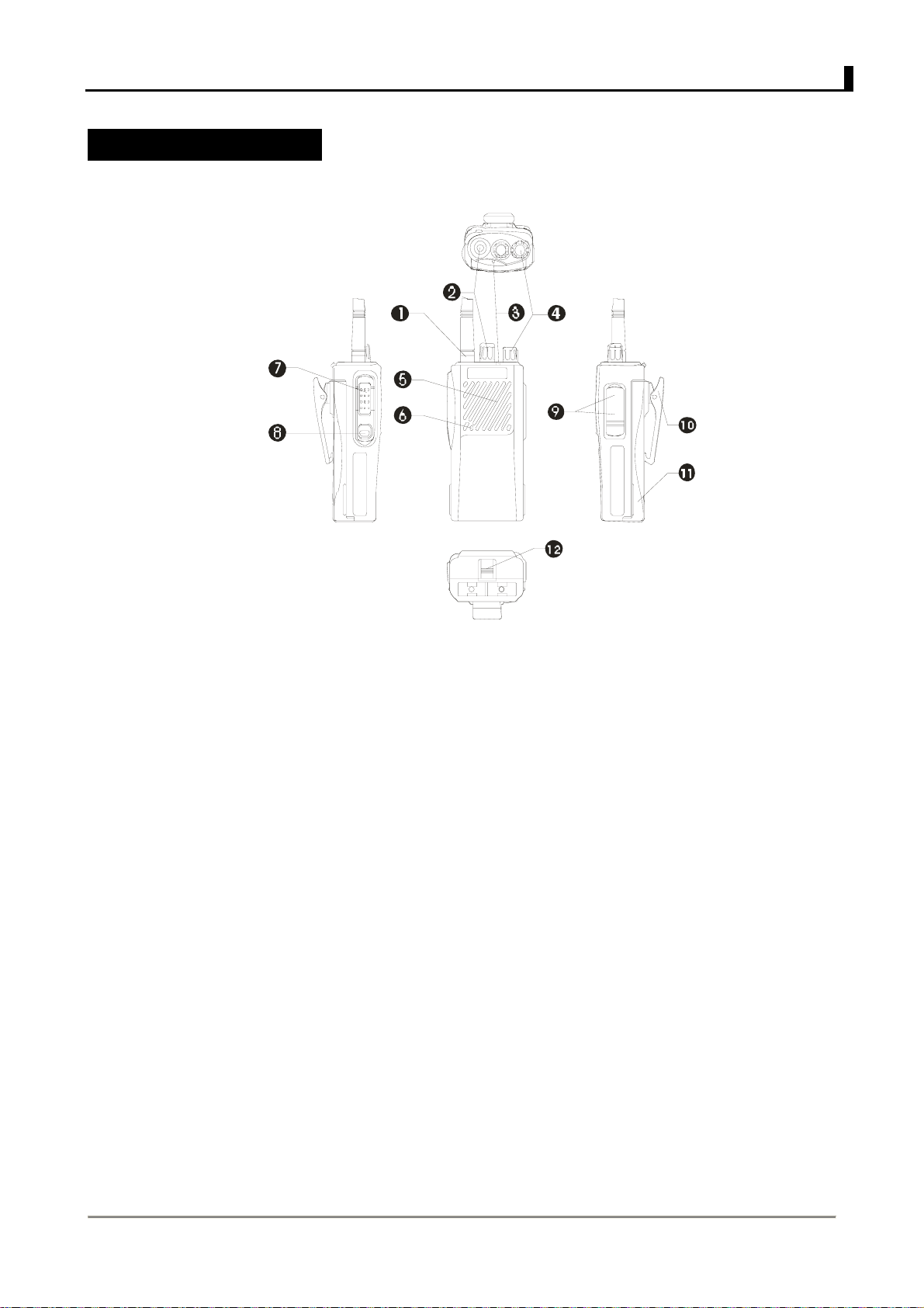
Brief Introduction
RPV516/RPU416 Brief Introduction
1. Mode
User mode: Turn on the power to enter the mode.
PC mode:Set and adjust radio data with PC software or programmer in this mode.
2. Parts description:
(1) Antenna
(2) Channel (frequency) selector knob
Turn the knob to choose channel from 1 to16 (Channel 16 can be set by the dealer as scan
function).
(3) LED indicator
Red LED glows while transmitting; green LED glows while receiving; red LED flashes when the
battery voltage is lower than the preset while transmitting.
(4) Power /Volume control knob
Turn the knob clockwise to turn on the power; turn the knob counter clockwise to turn off the power.
After the power is turned on, turn the knob to adjust the volume level.
(5) Speaker
(6) Microphone
(7) PTT (push to talk)
To transmit, hold down PTT and speak into the microphone; to receive, release PTT.
(8) Monitor key
Press the key to open squelch; release to close squelch.
(9) Speaker/microphone jack
(10) Belt clip
(11) Battery
- 2 -
Page 5
RPV516/RPU416 Circuit Description
Circuit Description
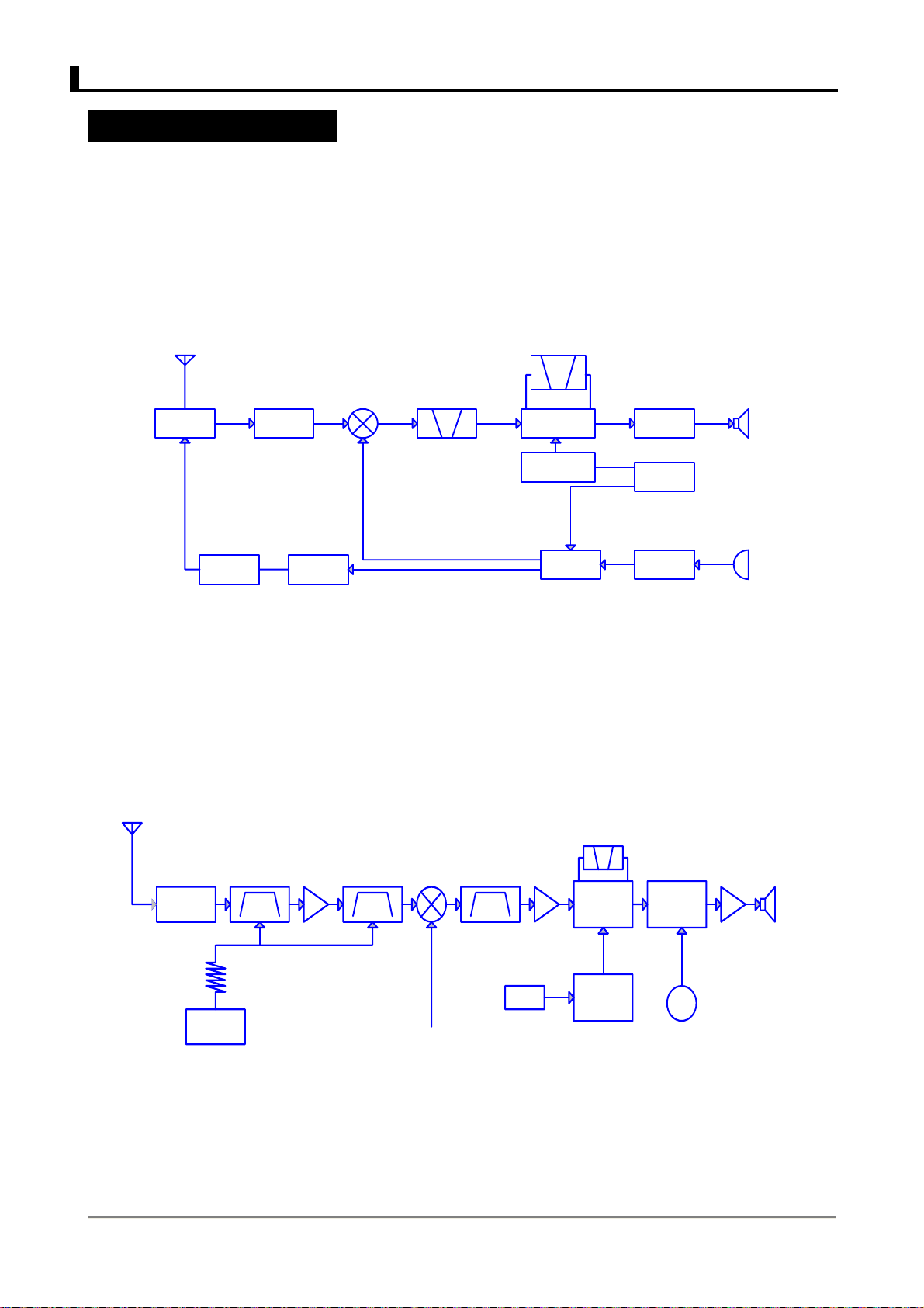
1. Frequency configuration
The receiver utilizes double conversion superheterodyne. The first IF is 38.85MHz and the second IF
is 450KHz. The first local oscillator signal is supplied by PLL circuit.
The PLL circuit in the transmitter generates the necessary frequencies. Fig.1 shows the frequencies.
RPV516 frequency range: RPV516 A: 150MHz—174MHz
RPU416 frequency range: RPU416 B: 400MHz—420MHz
RPU416 A: 450MHz—470MHz
ANT
ANTSW
MCF
RF
AMP AMP
38.85MHz
CF
450KHz
IF
SYSTEM
X3
multiply
AF
TCXO 12.8MHz
SP
CC
B
PA
AMP
TX
AMP
RX
TX
VCO
MICPLL
AMP
MIC
Fig. 1. Frequency configuration
2. Receiver
The receiver employs double conversion superheterodyne.
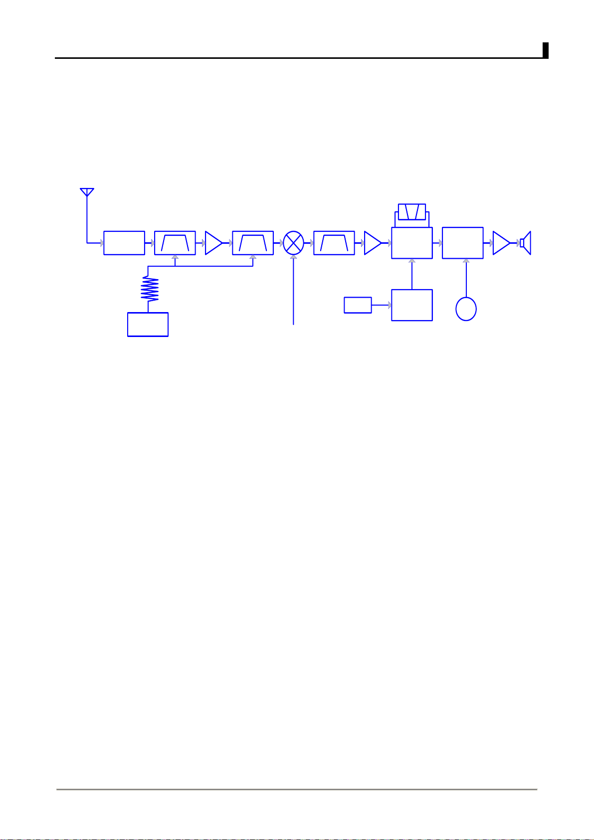
1-a) Front end RF amplifier (RPV516)
The input signal of antenna is applied to an RF amplifier (Q203) after passing through a
transmit/receive switch circuit and a 3-grade low pass filter. The amplified signal is filtered through a
band pass filter (a 3-grade LC filter) to eliminate unwanted signal before it is applied to the first mixer.
The voltage of varactor is provided by MPU (IC403). (See Fig. 2-a)
ANT
CF200
D102
D103
BPF
L208-L210
RF AMP
Q203
BPF
L214L215
MIXER
Q202
MCF
XF200
IF AMP
Q201
IF.MIX
IC200
AF AMP
LPF.HPF
IC300
TUNE
X3
APC
B
IC403
MCU
1st Local OSC
(PLL)
TCXO
multiply
Q1
Fig. 2-a. Receiver section configuration
AF PA AMP
IC302
SP
WIDE/NARROW SW
Q303
B
CC
B
- 3 -
Page 6
RPV516/RPU416 Circuit Description
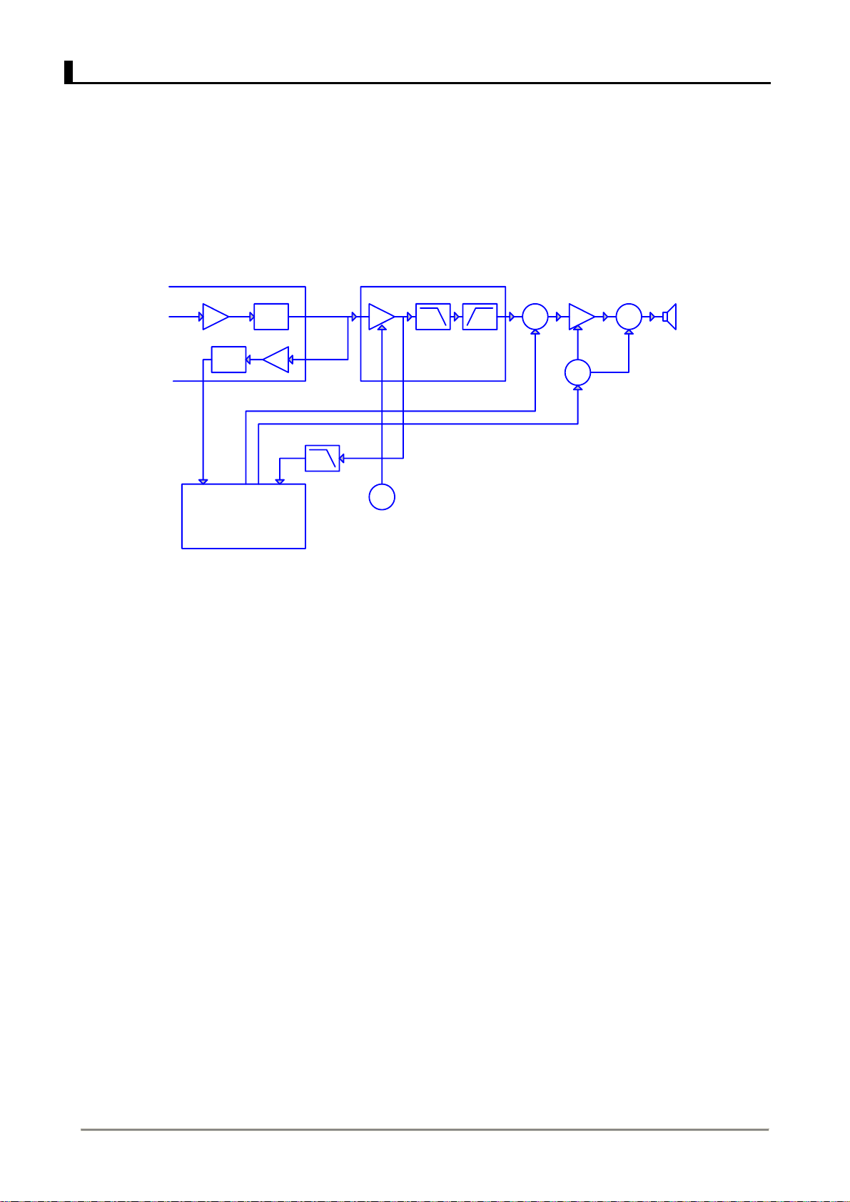
1-b) Front end RF amplifier (RPU416)
The input signal of antenna is applied to an RF amplifier (Q203) after passing through a
transmit/receive switch circuit and a 3-grade low pass filter. The amplified signal is filtered through a
band pass filter (a 3-grade LC filter) to eliminate unwanted signal before it is applied to the first mixer.
The voltage of varactor is provided by MPU (IC403). (See Fig. 2-b)
ANT
CF200
D102
D103 Q203
B
L208-L211
TUNE
APC
IC403
MCU
RF AMPBPF
BPF
L214-L215
MIXER
Q202
1st Local OSC
(PLL)
MCF
XF201
IF AMP
Q201
IF.MIX
IC200
X3
multiplyTCXO
Q1
AF AMP
LPF.HPF
IC300
AF PA AMP
IC302
WIDE/NARROW SW
Q303
Fig. 2-b. Receiver section configuration
2) First mixer
The signal from the RF amplifier is heterodyned with the first local oscillator signal from the PLL
frequency synthesizer circuit at the first mixer (Q202) to create a 38.85 MHz first IF (intermediate
frequency) signal. The first IF signal is then applied to two monolithic crystal filters (MCFS: XF200) to
further remove spurious signal.
3) IF amplifier
The first IF signal is amplified by Q201, and then enters IC200 (IF processing IC). The signal is
heterodyned again with a second local oscillator signal within IC200 to create a 450KHz second IF
signal. The second IF signal is then fed through a 450KHz ceramic filter (CF200) to further eliminate
unwanted signals before it is amplified and FM detected in IC200.
4) AF amplifier
The recovered AF signal obtained from IC200 is amplified by IC300 (1/4), filtered by the IC300
low-pass filter (2/4) and IC300 high-pass filter (4/4), and de-emphasized by R303 and C306. The
processed AF signal is then passed to a WIDE/NARROW switch (Q303) and its output is applied to
an AF volume control and is amplified to a sufficient level to drive a loud speaker by an AF power
amplifier (IC302).
CC
SP
B
- 4 -
Page 7
RPV516/RPU416 Circuit Description
5) Squelch
Part of the AF signal from IC200 re-enters IC200, and the noise component is amplified and rectified
by a filter and an amplifier to produce a DC voltage corresponding to the noise level.
The DC signal is injected to the analog port of the microprocessor (IC403). IC403 compares the
voltage with the preset value and determines whether to output sounds from the speaker. IC403
sends a high level signal to the MUTE and AFCO lines and turns IC302 on through Q302, Q304,
Q305, Q306 and Q307. (See Fig.3)
FM IF IC200
IF AMP DET
DET HPF
BUSY
MUTE
IC403
MPU
AMP
AFCO
IC301
LPF
562676
TI
IC 300
AF AMP LPF HPF
Q15
W/N SW
Q302SWIC302
AF/PF AMP
Q307
SW
Q304.Q305.Q306
SW
SP
Fig. 3. AF amplifier and squelch
6) Receiving signaling
CTCSS/CDCSS
IC200 output signal is filtered by 300Hz low-pass filter (IC301) and the filtered signal is input to the
microprocessor (IC403). IC403 determines whether the CTCSS or CDCSS matches the preset value,
and controls the MUTE and AFCO and the speaker sounds output according to the squelch results.
TTS
IC200 output signal is filtered by IC8 and then applied to the microprocessor (IC403). IC403 compares
TTS with the preset value and controls MUTE and AFCO and speaker output according to squelch
results.
3. PLL frequency synthesizer
PLL circuit generates the first local oscillator signal for reception and the RF signal for transmission.
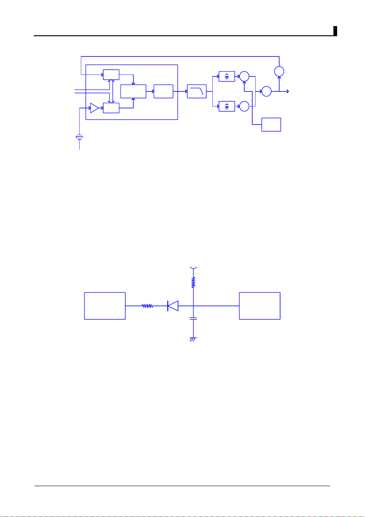
1) PLL
The frequency step of the PLL circuit is 2.5 or 6.25KHz. A 12.8MHz reference oscillator signal is
divided at IC1 by a mixed counter to produce 2.5 or 6.25KHz reference frequency. The voltage
controlled oscillator (VCO) output signal is buffer amplified by Q6, and then divided in IC1 by a
dual-module programmable counter. The divided signal is compared in phase with the 2.5 or 6.25KHz
reference signal in the phase comparator in IC1. The output signal from the phase comparator is
filtered through a low-pass filter and passed to the VCO to control the oscillator frequency. (See Fig. 4
of Next Page)
- 5 -
Page 8
C
PLL DATA
REF OSC
PLL IC IC1
5KHz/6.25KHz
I/N
COMPARATOR
I/M
5KHz/6.25KHz
PHASE
CHARGE
PUMP
RPV516/RPU416 Circuit Description
D2.4Q4TX VCO
LPF
D1.3Q3RX VCO
Q6
BUFF AMP
Q5.7
T/R SW
Q2
RF AMP
DD
C
B
12.8MHz
B
Fig. 4. PLL circuit
2) VCO
The operating frequency is generated by Q4 in transmit mode and Q3 in receive mode. The oscillator
frequency is controlled by applying the VCO control voltage, obtained from the phase comparator, to
the varactor diodes (D2 and D4 in transmit mode and D1 and D3 in receive mode). The T/R pin is set
high in receive mode causing Q5 and Q7 to turn Q4 off, and turn Q3 on. The T/R pin is set low in
transmit mode. The outputs from Q3 and Q4 are amplified by Q6 and sent to the buffer amplifiers.
3) Unlock Detector
If a low level signal appears at the LD pin of IC1, an unlock condition occurs, and the DC voltage
obtained from D7, R6, and C1 causes the voltage applied to the UL pin of the microprocessor to go
low. When the microprocessor detects this condition, the transmitter is disabled, ignoring the
push-to-talk switch input signal. (See Fig. 5)
5C
R6
IC1
D7
LD
IC403
UL
PLL IC
C1
MPU
Fig. 5. Unlock detector circuit
4. Transmitter
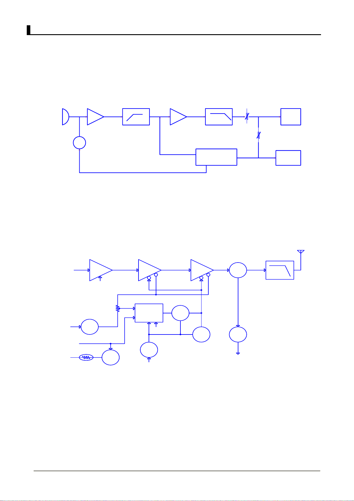
1) Transmit audio
The modulation signal from the microphone is amplified by IC500 (1/2), and then passes through a
pre-emphasis circuit and a 300Hz low-pass filter (Q501 and Q502). The resulting signal goes to the
VCO for direct FM modulation. (See Fig. 6)
2) CTCSS/CDCSS encoder
A necessary signal for CTCSS/CDCSS encoding is generated by IC403 and FM-modulated to the PLL
reference signal. Since the reference OSC does not modulate the loop characteristic frequency or
higher, modulation is performed at the VCO side by adjusting the balance. (See Fig. 6)
- 6 -
Page 9
RPV516/RPU416 Circuit Description
ANT
3) TTS encoder
The necessary signal for TTS encoding is generated by IC403. The signal is sent to IC500 (1/2), and
then applied to 3KHz low-pass filter (Q501 and Q502). The resulting signal is applied to VCO for direct
modulation (See fig. 6).
MIC
IC500(1/2)
MIC
AMP
Q503
SW
PREEMPHASIS
IC500(1/2)
TTS
IDC
Q501.502
LPF
(SPATTER FILTER)
IC403
TTS
MUTE
TO
CTCSS/CDCSS
VR501
MAX
DEV
VR500
BALANCE
D5.Q4
VCO
X1.IC1
PEFERENCE
OSC
Fig. 6. Transmit audio CTCSS/CDCSS
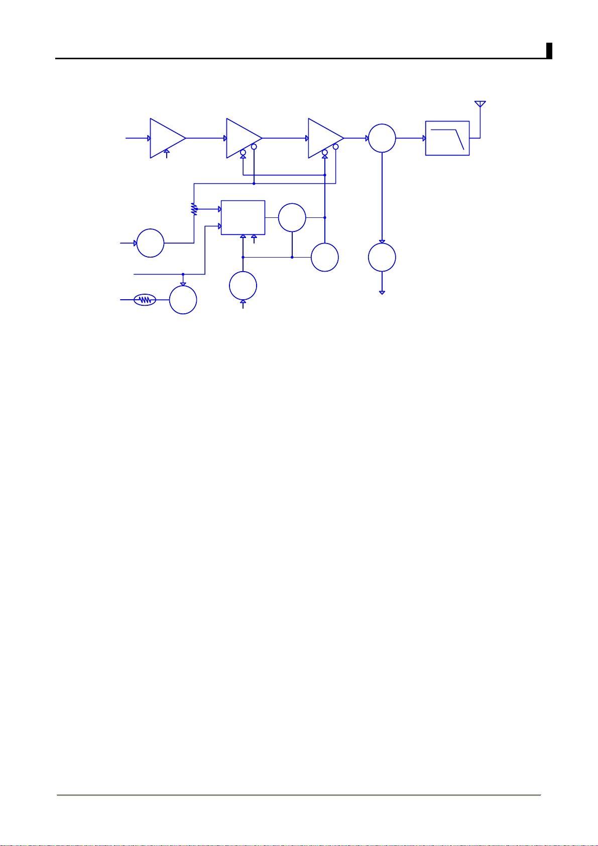
4-a) RF amplifier (RPV516)
The RF signal obtained from the VCO buffer amplifier Q100 is amplified by Q101 and Q102. This
amplified signal is passed to the power amplifier, Q102 and Q105, which consists of a 2-stage FET
amplifier and is capable of producing up to 4.5W of RF power (See Fig. 7-a).
AMP
Q103.Q104
B SW
TH100
Q101
5T
DET
SW
Q107
D
C
B
B
APC
5T
A
DRIVE AMP
Q102
APC
IC100
5T
5T
Q108
SW
Q109
SW
FINAL AMP
Q105
Q106
SW
ANT SW
D101 LPF
ANT SW
D102.103
RX
Title
Number RevisionSize
Fig. 7-a. APC system
4-b) RF amplifier (RPU416)
The RF signal obtained from the VCO buffer amplifier Q100 is amplified by Q101 and Q102. This
amplified signal is passed to the power amplifier, Q105 and Q107, which consists of a 2-stage FET
amplifier and is capable of producing up to 4W of RF power (See Fig. 7-b)
- 7 -
Page 10
RPV516/RPU416 Circuit Description
ANT
AMP
D
C
Q101.102
5T
DET
Q103.Q104
B SW
DRIVE AMP
Q105
APC
IC100
Q109
SW
FINAL AMP
Q107
ANT SW
D101 LPF
B
B
APC
TH102
5T
A
SW
Q110
5T
Q108
SW
5T
Q106
SW
RX
ANT SW
D102.103
Title
Number RevisionSize
Fig. 7-b. APC system
5) ANT switch and LPF
The RF amplifier output signal is passed through a low-pass filter network to filter the second
harmonic components and then applied to a transmit/receive switching circuit before it is passed to
the antenna terminal. The transmit/receive switching circuit is comprised of D101, D102 and D103.
D102 and D103 is turned on (conductive) in transmit mode and off (isolated) in receive mode.
6) APC
The automatic power control (APC) circuit stabilizes the transmitter output power at a predetermined
level by sensing the drain current of the final amplifier Field Effect Transistor (FET). The voltage
comparison circuit compares the voltage obtained from the above drain current with a reference
voltage which is set using the microprocessor. The APC voltage is proportional to the difference
between the sensed voltage and the reference voltage output from IC100 (1/2). This output voltage
controls the gate of the FET power amplifier, which keeps the transmitter output power be varied by
the microprocessor which in turn changes the reference voltage and hence, the output power.
7) Temperature protection circuit
When the thermistor (TH102) reaches about 80℃, the protection circuit turns on Q110 to protect
transmitting final amplifier (Q107).
5. Power supply
A 5V reference power supply [5M] for the control circuit is derived from an internal battery. This
reference power supply is used to provide a 5V supply in transmit mode [5T], a 5V supply in receive
mode [5R], and a 5V supply common in both modes [5C] based on the control signal sent from the
microprocessor.
6. Control system
The IC403 CPU operates at 7.37MHz. This oscillator has a circuit that shifts the frequency according
to the EEPROM data.
- 8 -
Page 11

RPV516/RPU416 Software Specifications
Software Specifications
Ⅰ.Specifications:
1. Use mechanical knob to choose from 16 channels.
Frequency: VHF: 150~174MHz UHF: 400~420MHz UHF: 450~470MHz
2. Monitor
3. Auto power saving
4. Audio alarm
5. Auto squelch control (1~9 level)
6. Timing
7. Channel spacing 25KHz/12.5KHz (Wide/Narrow)
8. CTCSS, CDCSS and TTS encode
9. CTCSS, CDCSS and TTS decode
10. Busy channel lockout
11. Clock frequency offset
12. Scan
13. PC mode
14. PC adjusting mode
15. Wired clone
16. Manual adjusting mode
Ⅱ.Description:
1. User mode: conventional communications mode
2. PC mode:
The following parameters can be set by using external programmer or PC programming
software:
(1) Receive frequency & Transmit frequency
(2) Receive signaling & Transmit signaling
(3) Busy channel lockout
(4) Clock frequency offset
(5) TOT
(6) Squelch level
(7) Power saving
(8) Audio alarm
(9) Channel spacing 25KHz/12.5KHz(Wide/Narrow)
(10) Monitor mode
(11) Scan mode
(12) Scan revert channel
(13) Priority scan channel
3. PC adjusting mode:
The following parameters can be set by using external programmer or PC programming
software:
(1) Transmit power output
(2) Low battery warning level
(3) Squelch level (level 9 and level 3)
(4) CTCSS deviation (Wide/Narrow).
(5) CDCSS deviation (Wide/Narrow).
(6) Receive sensitivity(at low、center、high frequency)
- 9 -
Page 12

PV516/RPU416 Software Specifications
4. Wired Clone:
Turning on the power while holding down MONI, the radio enters wired clone mode after 2 seconds.
Press PTT, red LED blinks, and cloning begins; when cloning is completed, red LED goes out.
5. Model set mode:
(1) Complete the two SELF points (short circuit) on PCB, and turn on the power, two “Beeps” are
sounded.
(2) Set channel selector knob to corresponding position (1-16) according to the model (see initial
data table)
(3) Press [PTT] while holding down [MONI] to set the model. Channel data and settings are
initialized.
(4) Turn off the power, and disconnect the two SELF points on PCB to end the model settings. E.g.
RPV516A, its No. is 2, to initialize its model and channel data: short out the two SELF points
on PCB , and turn on the power, set the channel selector knob at CH2, and then press PTT
while holding down MONI, channel data of CH1,CH2,CH3 and CH4 is initialized as the
corresponding data of No.2. The receive and transmit frequencies of channel 5-14 are same
as channel 1, and the tone of CH5 and CH10 is 67.0Hz; CH6 and CH11 is 151.4Hz; CH7 and
CH12 is 250.3Hz; the code of CH8 and CH13 is 423(CDCSS); CH9 and CH14 is
-423(CDCSS). Channel 1-9 are wide, Channel 10-14 are Narrow. Turn off the power after
reset, disconnecting the two SELF points and restart the power to use the radio.
(5) Remarks:
The old data (frequency, CTCSS/CDCSS, channel function settings) will be deleted once the
new model is set, and part of functions will also be changed. Therefore, do not make this
operation unless it’s very necessary, such as changing the EEPROM, etc.
- 10 -
Page 13

(6) Initial data table:
Initial
No. model Frequency (MHz)
1 136.000~149.995 140.000 +38.85 143.100 143.100 143.000 143.100 136.000 136.100 149.975 149.900
2 RPV516A 150.000~173.995 150.000 +38.85 162.100 162.100 162.000 162.100 150.000 150.100 173.975 173.900
3 RPU416B 400.000~419.995 410.000 -38.85 410.100 410.100 410.000 410.100 400.000 400.100 419.975 419.900
4 RPU416A 450.000~469.995 450.000 -38.85 460.100 460.100 460.000 460.100 450.000 450.100 469.975 469.900
5 350.000~369.995 360.000 -38.85 360.100 360.100 360.000 360.100 350.000 350.100 369.975 369.900
6 370.000~389.995 380.000 -38.85 380.100 380.100 380.000 380.100 370.000 370.100 389.975 389.900
7 220.000~239.995 230.000 -38.85 230.100 230.100 230.000 230.100 220.000 220.100 239.975 239.900
8 240.000~259.995 250.000 -38.85 250.100 250.100 250.000 250.100 240.000 240.100 259.975 259.900
9 406.000~429.995 410.000 -38.85 418.100 418.100 418.000 418.100 406.000 406.100 429.975 429.900
144.000~147.995 145.000 +38.85 146.100 146.100 146.000 146.100 144.000 144.100 147.975 147.900
11 336.000~367.995 350.000 -38.85 352.100 352.100 352.000 352.100 336.000 336.100 367.975 367.900
12 268.000~395.995 380.000 -38.85 382.100 382.100 382.000 382.100 268.000 268.100 395.975 395.900
13 430.000~439.995 430.000 -38.85 435.100 435.100 435.000 435.100 430.000 430.100 439.975 439.900
14 438.000~449.995 440.000 -38.85 444.100 444.100 444.000 444.100 438.000 438.100 449.975 449.900
15 465.000~494.995 480.000 -38.85 480.100 480.100 480.000 480.100 465.000 465.100 494.975 494.900
16 490.000~519.995 500.000 -38.85 505.100 505.100 505.000 505.100 490.000 490.100 519.975 519.900
frequency
(MHz)
IF (MHz)
Tx(MHz) Rx(MHz) Tx(MHz) Rx(MHz) Tx(MHz) Rx(MHz) Tx(MHz) Rx(MHz)
1CH 2CH(center) 3CH(low) 4CH(high)
Initialization data of channel 1-4 is in the above table CH1-CH4, the adjusting settings are reset to initial data. Tx and Rx frequencies of CH5~CH14 are the
same with CH1. The tone of CH5 and CH10 is 67.0Hz; the tone of CH6 and CH11 is 151.4Hz; the tone of CH7 and CH12 is 250.3Hz; the code of CH8 and
CH13 is 423(CDCSS); the code of CH9 and CH14 is -423(CDCSS). CH1~CH9 are Wide, CH10~CH14 are Narrow.
- 11 -
Page 14
RPV516/RPU416 Software Specifications
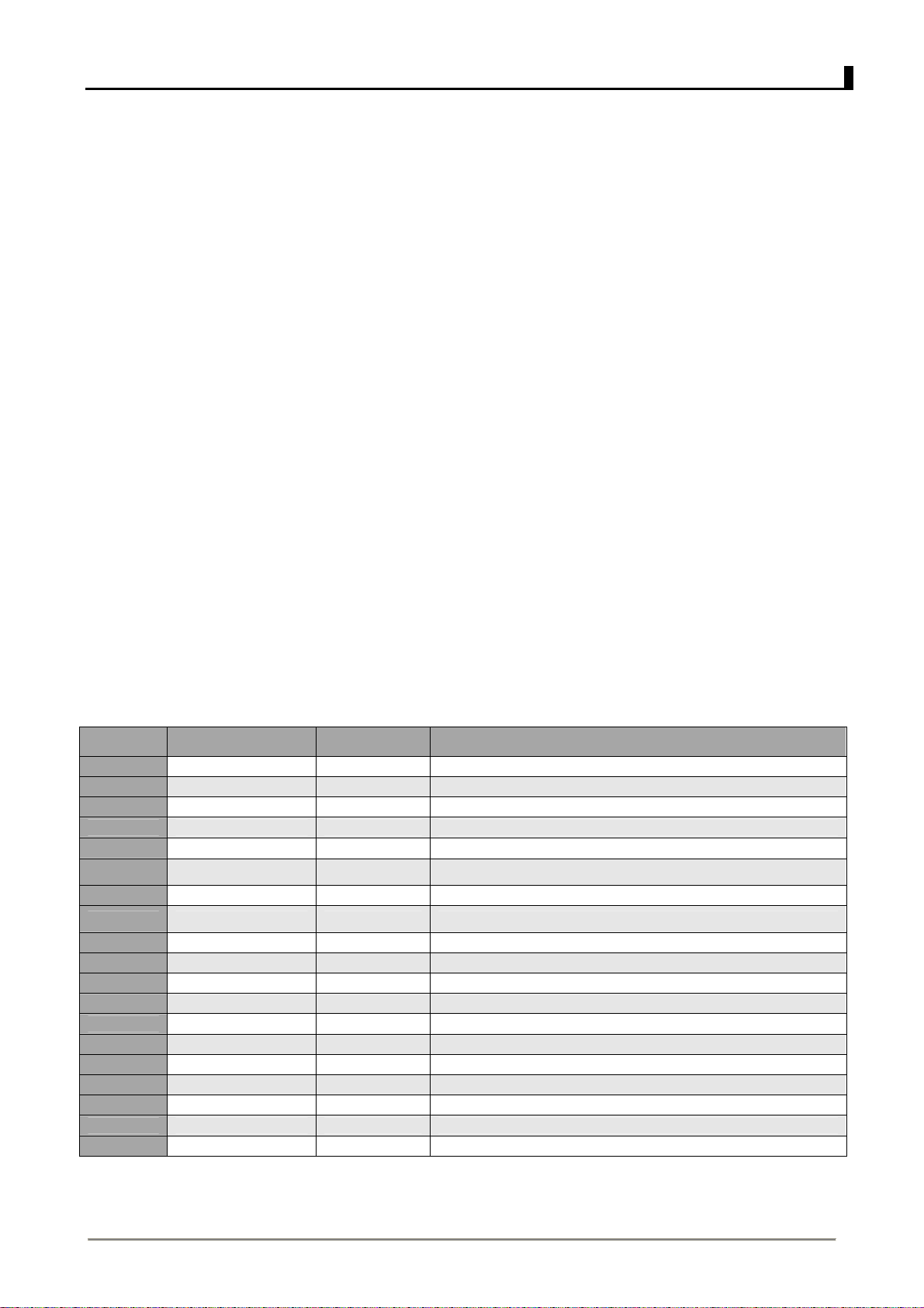
6. Manual Adjust Mode:
Turn on the power while pressing PTT and MONI simultaneously,the radio enters manual adjust
mode after 3 seconds. Choose the settings by turning the channel selector knob to CH1-CH12
position; use PTT (upwards) or MONI (downwards) to adjust (Note: MIC jack shouldn’t be
connected with external cable while adjusting), CH1-CH12 positions are defined as follows:
(1) TTS deviation
(2) Transmit power output
(3) Low battery warning level
(4) Receive sensitivity (adjust at center frequency)
(5) Receive sensitivity (adjust at low frequency)
(6) Receive sensitivity (adjust at high frequency)
(7) Squelch level (level 9)
(8) Squelch level (level 3)
(9) CTCSS deviation (Wide)
(10) CTCSS deviation (Narrow)
(11) CDCSS deviation (Wide)
(12) CDCSS deviation (Narrow)
CH13-CH16 are used for adjusting transmitter and receiver. Press PTT to transmit; Press
MONI to choose wide or narrow, one Beep means Narrow, two Beeps mean Wide. CH13~
CH 16 are defined as follows:
(13) Center frequency (difference between transmit and receive frequency is 0.1MHz).
(14) Lowest frequency (difference between transmit and receive frequency is 0.1MHz).
(15) Highest frequency (difference between transmit and receive frequency is -0.075MHz).
(16) Center frequency: transmit with 250.3Hz CTCSS tone (difference between transmit and
receive frequency is 0.1MHz).
Note:
To enable or disable manual adjust mode: short out the two SELF points, turn on the power, and the
manual adjust mode is enabled; press [PTT], manual adjust mode is disabled. This mode is
suggested to be disabled after the adjustment is completed.
III. CPU:
CPU control M38034M4
Pin No. Port name I/O Function
1 TI I CTCSS/CDCSS input
2 BUSY I Input busy signal
3 BATT I Detect battery voltage
4 NC I NC
5 TO O Output CTCSS/CDCSS
6 BEEP O Beep output
7 2TN I TTS input
8 ENC0 I Input encode
9 ENC1 I Input encode
10 ENC2 I Input encode
11 ENC3 I Input encode
12 NC I NC
13 PTT I [PTT] input, connect with RXD
14 TXD O RS-232C output
15 RXD I RS-232C input
16 MONI I [MONI] input
17 SELF I Self-Program L: set up model
18 CNVSS I Connect VSS
19 RST I Reset input
- 11 -
- 12 -
Page 15
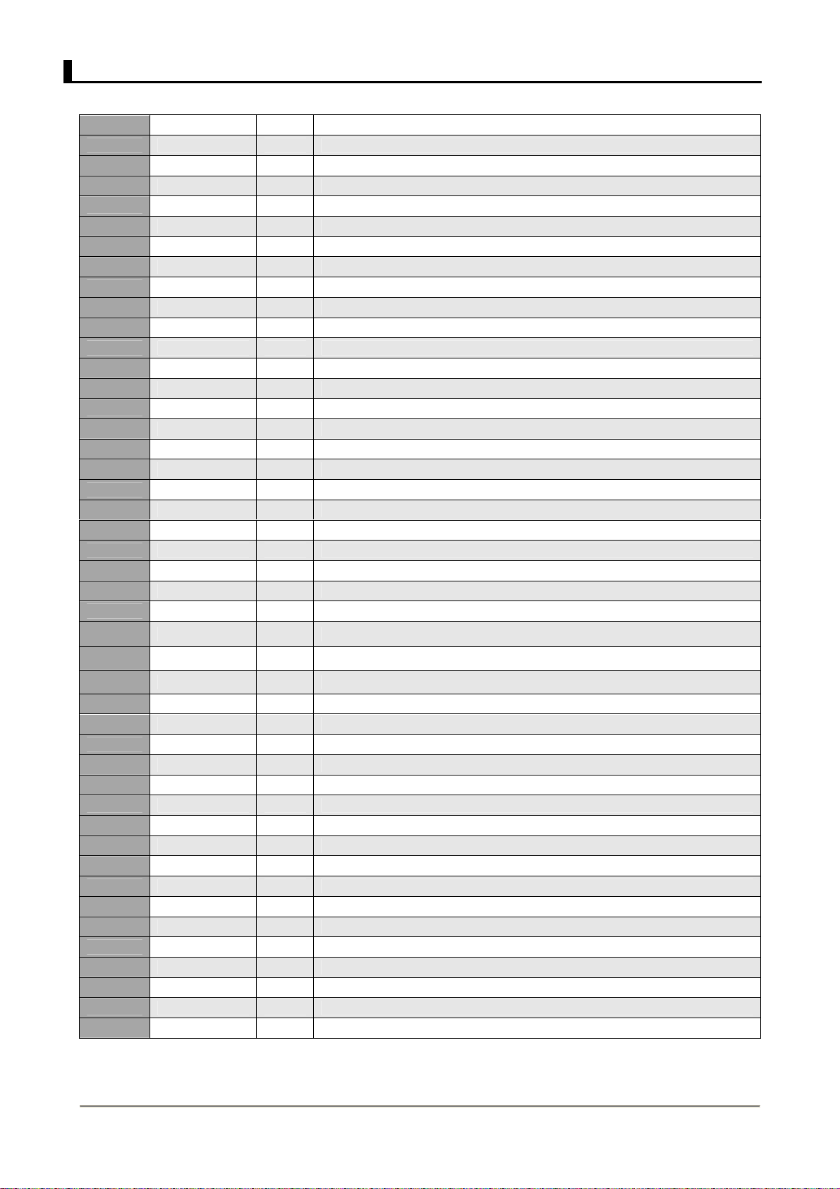
RPV516/RPU416 Software Specifications
20 INT0 I Power detection
21 NC I NC
22 XIN I Oscillator (7.3728MHz)
23 XOUT O Oscillator
24 VSS I Grounding
25 SHIFT O Clock frequency shift H: unlock
26 PABC O MOS FET power H: unlock
27 WNRC O Audio reference sensitivity L: narrow
28 WNTC O Max deviation control H: narrow
29 NC I NC
30 SDA I/O EEPROM data cable
31 SCL O EEPROM clock cable
32 UL I PLL unlock detector L: unlock
33 DT O Common data output
34 CK O Common clock output
35 LE O PLL IC H: lock up
36 5MC O Power control except CPU and EEPROM L: unlock
37 AFCO O AF amplifier H: unlock
38 RX O TX/RX VCO H: receive
39 GLED O Green light control H: light
40 RLED O Red light control H: light
41 SAVE O Power saving control H: power saving OFF
42 MUTE O mute control H: mic squelch L: AF squelch
43 5RC O Receiver power control L: unlock
44 5TC O Transmitter power control H: unlock
45 NC I NC
46 NC I NC
47 NC I NC
48 NC I NC
49 NC I NC
50 NC I NC
51 NC I NC
52 NC I NC
53 NC I NC
54 NC I NC
55 2TO O TTS output
56 APC O TX: APC output RX: BPF tune output
57 VCC I CPU power supply 5V
58 VREF I Connect with VCC
59 AVSS I Connect with VSS
60 NC I NC
61 NC I NC
62 NC I NC
63 NC I NC
64 TIBI I CTCSS/CDCSS exterior circuit central point input
- 13 -
Page 16
RPV516/RPU416 Adjustment Description
Adjustment Description
Program RPV516/RPU416 by using programmer or PC software, or by manual adjustment. Now explain
how to adjust RPV516/RPU416 in manual adjust mode (refer to “software descriptions” for the manual
adjust mode and model set).
Ⅰ. Instruments:
1. Communication analyzer 1 set
2. Spectrum analyzer 1 set
3. 3A/10V power source 1 set
4. Digital Voltmeter 1 set
5. 3A Ammeter 1 set
Ⅱ. Adjustment:
1.Initialization:
It is necessary to initialize the radio because there is no useful data in EEPROM after it’s
assembled. Short out the SELF points on PCB, turn on the power and two beeps sound, place the
channel selector knob at CH2 [RPV516A], CH3 [RPU416 B] or CH4 [RPU416A], then press [PTT]
while holding [MONI], the channel data and function settings are initialized. Please refer to the
chapter “software descriptions”.
2. Adjustment:
The adjustment of RPV516/RPU416, some are adjusted in user mode, some are in manual adjust
mode. Turn on the power, the radio enters the user mode. While pressing PTT and MONI
simultaneously, turn on the radio,the radio enters the manual adjust mode in 3 seconds. (Refer to
the manual adjust mode in chapter of “software descriptions”).
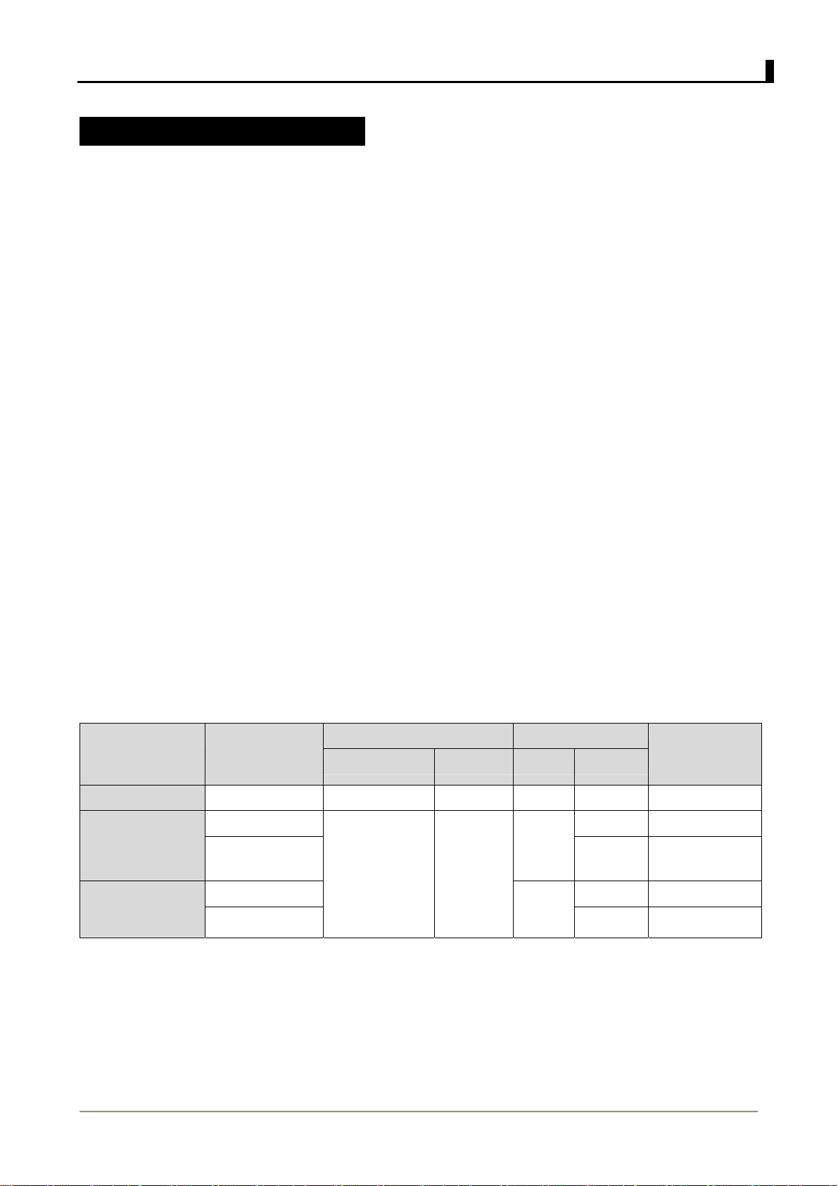
VCO Section:
Measurement Adjustment
Item Condition
1.Setting Power 7.5V
1.CH: TX HIGH 3.7V±0.1V
2.Transmit VCO lock
voltage
3.Receive VCO lock
voltage
2.CH: TX LOW
1.CH: RX HIGH 3.7V±0.1V
2.CH: RX LOW
Test equipment Terminal Part Method
Digital Voltmeter CV
TC1
TC2
Check
Check
Specifications/Re
marks
RPV516>0.7V
RPU416>1V
RPV516>0.7V
RPU416>1V
Note:
Whether VCO is unlocked can be checked in manual adjust mode. (Signal can be transmitted in manual
mode regardless of the VCO locked or unlocked).
- 14 -
Page 17
RPV516/RPU416 Adjustment Description
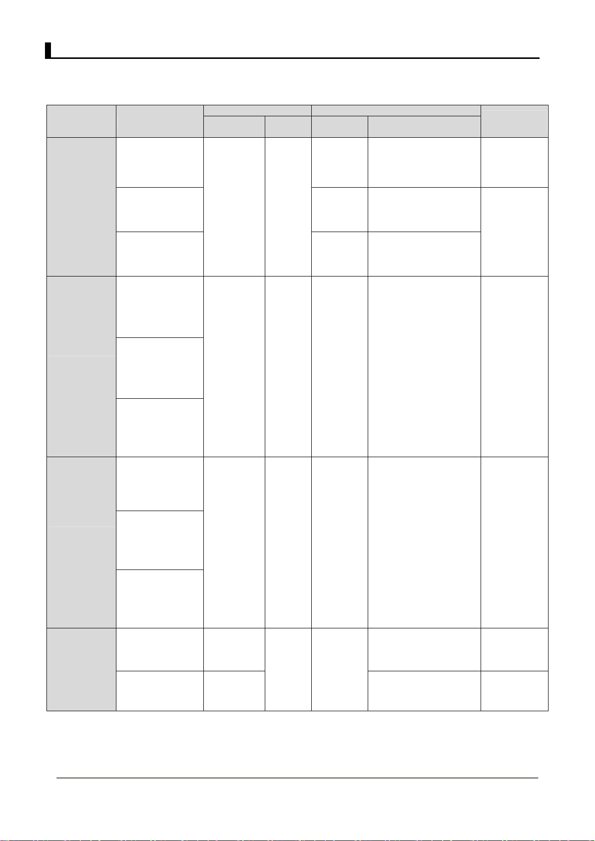
Adjust the receiver section: (in manual adjust mode)
Item Condition
1. CH:RX Center
Turn to channel 4 in
manual mode.
4. RF amplifier
BPF
5.Sensitivity
(Wide)
2. CH: RX Low Turn
to channel 5 in
manual mode.
3.CH:RX High 3Turn
to channel 6 in
manual mode
1. CH: RX Center.
Turn to channel 13 in
manual mode.
Channel spacing:
Wide
2. CH: RX Center
Turn to channel 14 in
manual mode.
Channel spacing:
Wide
3. CH: RX Center
Turn to channel 15 in
manual mode.
Channel spacing:
Wide
Measurement Adjustment
Test
equipment
Spectrum
analyzer
Communication analyzer
SSG output :
-118dBm
MOD:1KHz
DEV:±3KHz
FILTER:
0.3-3.4KHz
Terminal Parts Method
TC201
TC202
(RPU416)
TC203
(RPU416)
PTT
ANT. TP2
ANT SP Check
(upwards)
MONI
(downwards)
PTT
(upwards)
MONI
(downwards)
Adjust the waveform to the
top, and the top is flat, the
bandwidth is about 10MHz,
the sign of RX central
frequency is at the middle
of the waveform.
Adjust the waveform to the
top, the sign of RX low
frequency is on the left of
the waveform top.
Adjust the waveform to the
top; the sign of RX high
frequency is on the right of
the waveform top.
Specifications/
Remarks
SINAD: 12dB
or higher
6. Sensitivity
(Narrow)
7. Squelch
1. CH: RX center
Turn to channel 13 in
manual mode.
Channel spacing:
narrow
2. CH: RX center
Turn to channel 14 in
manual mode.
Channel spacing:
narrow
3. CH: RX center
Turn to channel 15 in
manual mode.
Channel spacing :
narrow
1.CH: RX center
Turn to channel 7 in
manual mode
2. CH: RX center.
Turn to channel 8 in
manual mode.
Communication analyzer
SSG output:
-116dBm
MOD:1KHz
DEV:±1.5KHz
FILTER:
0.3-3.4KHz
Communication analyzer
SSG output :
-117dBm
Communication analyzer
SSG output :
-125dBm
ANT SP Check
Level 9
Level 3
ANT SP
PTT
(upwards)
MONI
(downwards)
Adjust to close the squelch.
Adjust to close the squelch.
SINAD: 12dB or
higher
Adjust squelch
level 9
Adjust squelch
level 3
- 15 -
Page 18
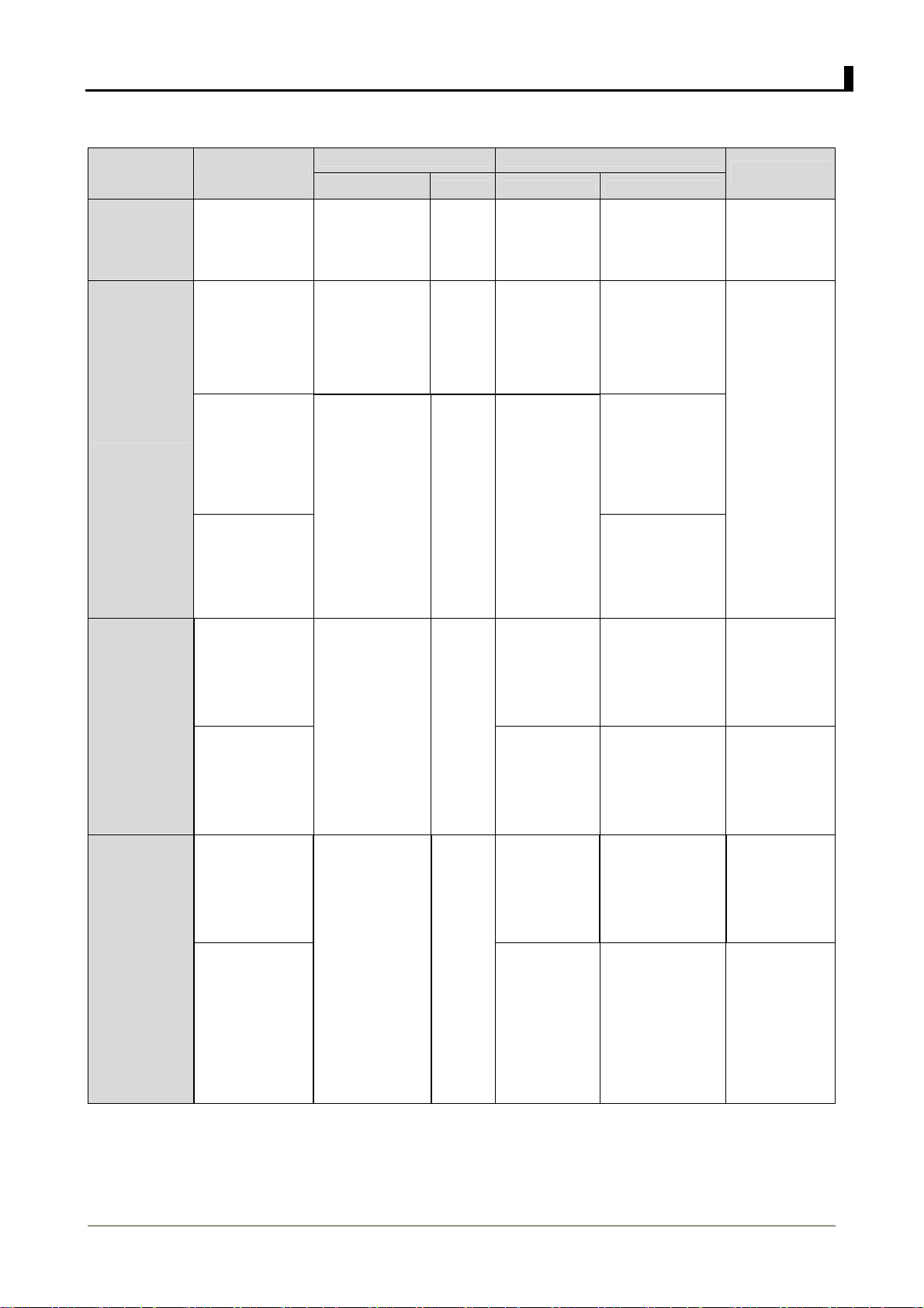
Adjust the transmitter section:
Item Condition
RPV516/RPU416 Adjustment Description
Measurement Adjustment
Test
equipment
Terminal Parts Method
Specifications
/Remarks
8.Transmit
frequency
9. Power
10. Max
Deviation
CH: TX Center
Turn to channel
1 in manual
mode.
1.CH:TX Center
Turn to channel
2 in manual
mode.
2.CH: TX Low
Turn to channel 3
Press PTT
3.CH:TX High
Turn to channel 4
Press PTT
1. CH: TX Center
Turn to channel
13 in manual
mode. Channel
spacing: wide
Press PTT
.
2. CH: TX Center
Turn to channel
13 in manual
mode. Channel
spacing: narrow
Press PTT
Communication
analyzer
Communication
analyzer
Ammeter
Communication
analyzer
LPF:15KHz
AF:1KHz
120mV
ANT VR1
PTT
ANT
ANT
MIC
(upwards)
MONI
(downwards)
VR501
Adjust it to center
frequency
Adjust it to:
4.0 W≤Po≤4.8W
(RPV516)
3.7 W≤Po≤4.7W
(RPU416)
I≤1.6A
Adjust it to:
4.0 W≤Po≤4.8 W
(RPV516)
3.7 W≤Po≤4.7 W
(RPU416)
I≤1.6A
Adjust it to:
4.0 W≤Po≤4.8 W
(RPV516)
3.7 W≤Po≤4.7 W
(RPU416)
I≤1.6A
Adjust deviation to:
4.2KHz±100Hz
Check:
1.8KHz-2.2KHz
Error<150Hz
Wide
Narrow
11.MICSENS
1. CH: TX Center
Turn to channel
13 in manual
mode. Channel
spacing: wide
Press PTT
2. CH: TX Center
Turn to channel
13 in manual
mode.
Channel spacing:
narrow
Press PTT
Communication
analyzer
FILTER:
0.3-3.4KHz
AF:1KHz
+12mV
ANT
MIC
- 16 -
VR501
Check:
2.2KHz-3.6KHz
Check:
1.1KHz-1.8KHz
Wide
Narrow
Page 19

RPV516/RPU416 Adjustment Description
Item Condition
1.CH:TX center,
turn to channel 9
in manual mode
12.CDCSS/
CTCSS
13.CTCSS
Deviation
14.CDCSS
Deviation
2. CH: TX Center
Turn to channel 16
in manual mode.
Press PTT.
1. CH: TX Center
Turn to channel 9
in manual mode.
2. CH: TX Center
Turn to channel 10
in manual mode.
1. CH: TX Center
Turn to channel 11
in manual mode.
2. CH: TX Center
Turn to channel 12
in manual mode.
Measurement Adjustment
Test
equipment
Communication
analyzer LPF:
300Hz
Communication
analyzer
LPF:300Hz
Terminal Parts Method
ANT VR500
PTT
ANT
(upwards)
MONI
(downwards)
Adjust VR500,
deviation tested on
condition 1 and
condition 2 are
consistent, the
difference≤20Hz
Adjust dev. to:
0.75KHz±50Hz
Adjust dev.
to:0.35KHz±50Hz
Adjust dev. to:
0.75KHz±50Hz
Adjust dev. to:
0.35KHz±50Hz
Specifications
/Remarks
67.0Hz
CTCSS
250.3Hz
CTCSS
Wide
Narrow
Wide
Narrow
15.Low
Battery
level
Turn to channel 3
in manual mode.
Adjust the power
supply voltage at
5.8V
16. TTS
deviation
Note:
In manual adjust mode, when channel selector knob is positioned at channel 1-channel12, MIC jack can’t connect with
external cables. After adjustment is completed, complete the two SELF points (short circuit),the radio enters model set
mode,then press PTT to disable the manual adjust mode.
CH: TX Center
Turn to channel 1
in manual mode.
Digital voltmeter
Communication
analyzer
LPF:15KHz
PTT
(upwards)
MONI
(downwards)
PTT
(upwards)
MONI
(downwards)
Adjust the level to
make the LED flash.
Adjust the dev. to:
3KHz±100Hz
Wide
- 17 -
Page 20
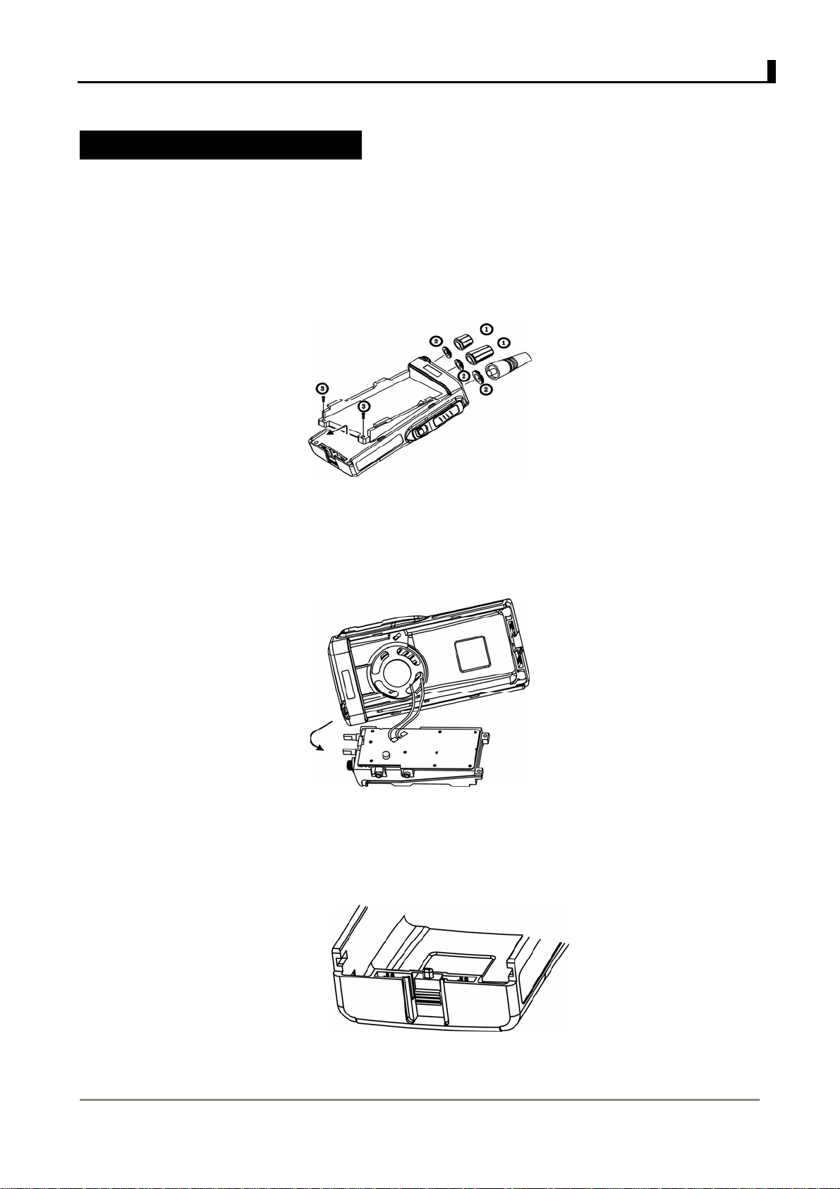
RPV516/RPU416 Disassembly for Repair
Disassembly for Repair
Separating the front cover assembly from the chassis
1. Remove the two knobs ① and three ring nuts ②.
2. Remove the two screws ③.
3. Expand the right and left sides of the bottom of the front cover assembly,lift the chassis, and remove
it from the front cover assembly.
4. Taking care not to cut the wire assembly connecting the speaker and chassis, separate the chassis
and the front cover assembly.
Removing the lever
Raise the lever on the bottom of the case, insert a small flat screwdriver into the space between the case
and lever, open the case carefully and lift the lever off.
Note: Do not force to separate the cover from the lever.
- 18 -
Page 21
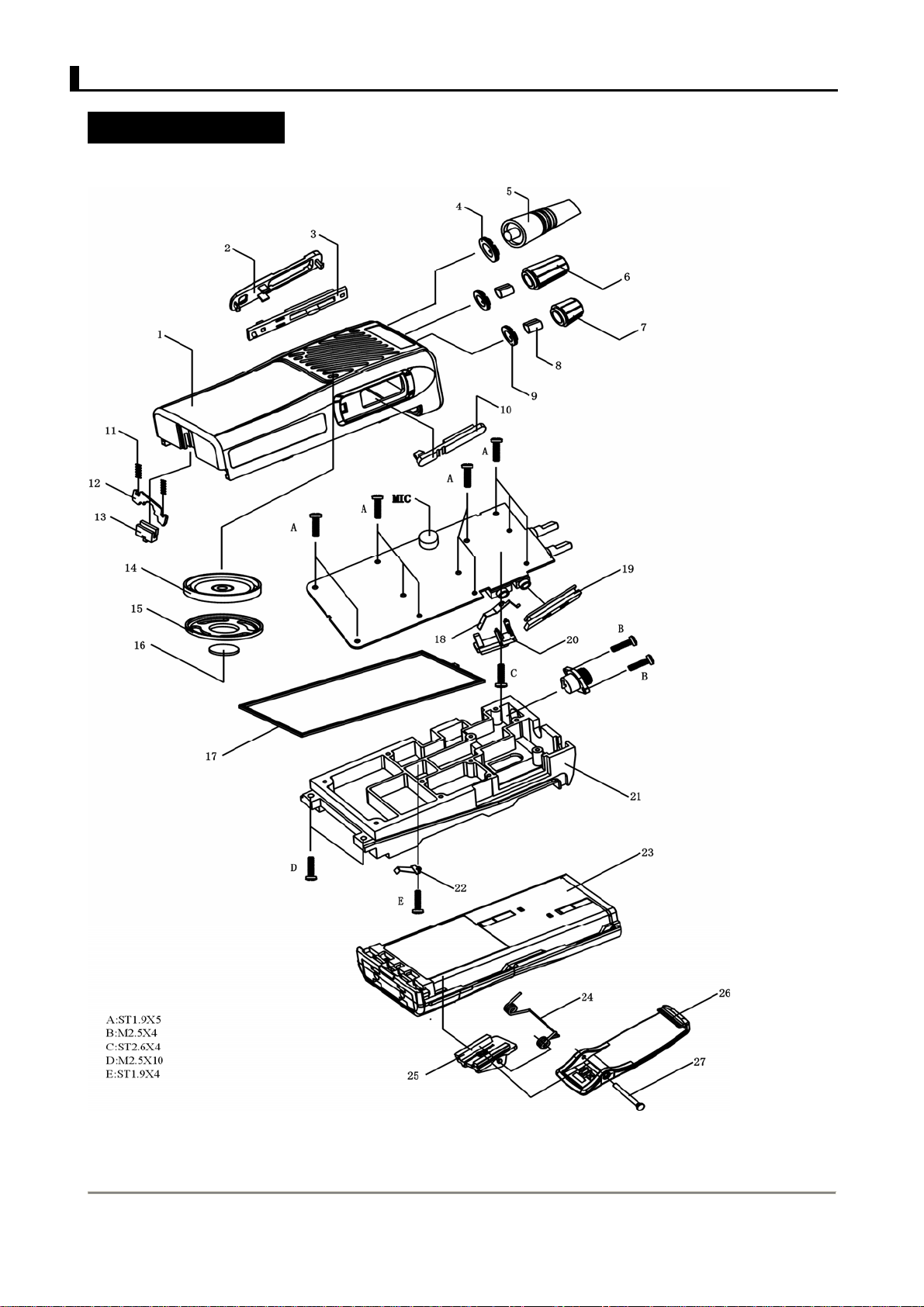
RPV516/RPU416 Exploded View
Exploded View
- 19 -
Page 22
RPV516 parts List
r
RPV516 Parts List
Ref. No. Material Code Description Address Destination Ref. No. Material Cod e Description Address Destination
1 1509103A front cover R25 1036812 680 B2F
2 1509105A bezel (ptt) R26 01034722 4.7K B2G
3 1609205A button(ptt) R27 01031022 1K B1F
4 1409302A
5 1509106A knob(enc) R29 01030002 0 B2C
6 1509107A knob(vol) R30 01033312 330 B2B
7 14013110 inner liner(knob) R100 01033322 3.3K B2F
8 14013190
9 1509102A panel(top) R101 01031232 12K B2F
10 1509104A water-resistant cap R102 01032212 220 B2F
11 14063080 spring R104 01031012 100 B2G
12 14063090 metal piece R106 01033322 3.3K B3F
13 15061090 latch (battery release) R108 01031522 1.5K B3F
14 1609203S speaker washer R109 01031002 10 B3G
15 13090020 speaker R110 01033312 330 B3F
16 16092020 MIC washer R112 01031802 18 B3F
17 1609206S
18 14063101
19 1609207S shroud(SP/MIC plug) R117 01034702 47 B3H
20 15061140
21 16094050 washer (holder) R119 01034722 4.7K T2J
22 14093100 socket (antenna) R120 01033322 3.3K B3G
23 1409309S
24 14063071 cathode piece R122 01036812 680 T2J
25 19090041 battery R124 01035612 560 T2H
26 14093060 spring(belt clip) R125 01033322 3.3K T2H
27 15091050 holder(belt clip) R126 01036812 680 T2J
28 15091040 belt clip R127 01032712 270 B4J
29 14093050 pin R128 01032712 270 B4J
R1 01031531 150K B1C R131 01050002 0.5 T2J
R2 01031022 1K B1C R132 01050002 0.5 T2J
R3 01031002 10 B2D R133 01031541 150K T1I
R4 01031022 1K B3D R134 01031541 150K T1I
R5 01030002 0 B1C R135 01031541 150K T1I
R6 01031022 1K T5C R136 01031541 150K T1I
R7 01030002 0 B1C R137 01031541 150K T1I
R8 01033342 330K B3D R138 01031541 150K T1I
R9 01036812 680 B1C R140 01031032 10K T2I
R10 01031512 150 B1D R141 01034732 47K T1I
R11 01034732 47K B3B R142 01031052 1M T2I
R12 01033932 39K B3B
R13 01031512 150 B1D R144 01033312 330 T2H
R14 01031012 100 B3D R145 01031842 180K T1I
R15 01031032 10K B1D R146 01031042 100K T1H
R16 01036832 68K B2E R147 01033312 330 B3F
R17 01031042 100K B2E R148 01033312 330 B3G
R18 01032712 270 B1F R200 01031002 10 B5C
R19 01034732 47K B2E R201 01033922 3.9K B3B
R20 01031022 1K B2D R202 01031842 180K B4B
R21 01031042 100K B2D R203 01033322 3.3K B4B
R22 01032712 270 B1E R204 01033322 3.3K B4B
R23 01031241 120K B2F R205 01038212 820 B5B
R24 01031042 100K B1F R206 01031842 180K B4B
nut (antenna base)
nut (switch)
(SPK/MIC ) R103 01031022 1K B2F
(battery release) R105 01033322 3.3K B3F
(battery release) R107 01033922 3.9K B3F
water-resistant ring
anode connecto
(battery)
holder(anode piece)
aluminum chassis
(battery) R123 01030002 0 B4I
R28 01030002 0 B1D
R114 01031541 150K B3G
R115 01034732 47K B3G
R116 01034702 47 B3G
R118 01030002 0 B3G
R121 01034732 47K B3G
R130 01050002 0.5 T2J
R143 01030002 0 T1H
- 20 -
Page 23
RPV516 Parts List
Ref. No. Material Code Description Address Destination Ref. No. Material Code Description Address Destination
R207 01031042 100K B5B R339 01038222 8.2K T1D
R208 01036842 680K B5C R340 01031241 120K B1B
R209 01032722 2.7K B5C R341 01031042 100K T1F
R210 01032212 220 B5C R400 01033342 330K T2B
R211 01034712 470 B3E R401 01031042 100K T4C
R212 01033302 33 B3E R402 01032212 220 B2K
R213 01030002 0 B5E R403 01031812 180 B2K
R214 01031032 10K B3E R404 01030002 0 T2B
R215 01034702 47 B3E R405 01031022 1K T4B
R216 01032222 2.2K B3E R406 01032222 2.2K B2J
R217 01030002 0 B3E R407 01031022 1K T2A
R220 01032222 2.2K B3E R408 01031042 100K T2A
R222 01030002 0 B4E R409 01031022 1K T3B
R223 01031012 100 B3E R410 01038222 8.2K B2K
R225 01031022 1K B3E R411 01032241 220K T2A
R226 01031042 100K B4E R412 01031002 10 T3B
R228 01034702 47 B5E R413 01031022 1K T2D
R229 01034712 470 B5E R414 01034732 47K T4K
R230 01031042 100K B5F R415 01034732 47K T4K
R231 01031512 150 B5F R416 01034722 4.7K T4C
R232 01030002 0 B5F R417 01031002 10 T4K
R233 01032241 220K B4F R418 01032222 2.2K T2C
R235 01031042 100K B4F R419 01030002 0 B2I
R237 01031042 100K B4F R420 01031022 1K B2I
R238 01031042 100K B4H R421 01034732 47K T4J
R239 01031042 100K B4H R422 01032722 2.7K B2H
R240 01030002 0 B4H R423 01034732 47K T4J
R300 01039131 91K B1B R424 01033322 3.3K B2I
R301 01035621 5.6K B3B R425 01033322 3.3K B2I
R302 01035621 5.6K B3B R426 01038222 8.2K B2K
R303 01033322 3.3K B2B R427 01031022 1K B2H
R304 01031052 1M B3B R428 01032722 2.7K B2H
R305 01031832 18K B2A R429 01038212 820 B2H
R306 01031241 120K B3A R430 01031012 100 T4J
R307 01034732 47K B2A R431 01030002 0 T4J
R308 01031032 10K B3A R432 01031032 10K B2H
R309 01034741 470K B3B R433 01031531 15K B2H
R310 01030002 0 T2F R434 01031531 15K B1H
R311 01030002 0 B3A R435 01031032 10K B2H
R312 01031232 12K B2B R500 01034722 4.7K T2C
R313 01033932 39K B3A
R314 01034741 470K B1B R502 01038232 82K T5C
R315 01033941 390K B1A R503 01036822 6.8K T2D
R316 01032241 270K B3A R504 01032232 22K T2D
R317 01032241 270K B2B R505 01036822 6.8K T2D
R318 01031842 180K B4A R506 01038212 820 T3E
R320 01034732 47K B3B R507 01034722 4.7K T4C
R321 01032232 22K B1B R508 01031022 1K T3E
R322 01032241 220K B2A R509 01031241 120K T2C
R323 01031042 100K B4A R510 01033322 3.3K T3E
R324 01035621 5.6K B1B R511 01031032 10K T3F
R325 01031042 100K B4A R512 01031852 1.8M T3E
R326 01035621 5.6K B1A R513 01031531 15K T2C
R327 01030002 0 T2E R514 01033332 33K T3E
R328 01031022 1K B1A R515 01033332 33K T3F
R329 01030002 0 B2A R516 01031032 10K T3F
R330 01034732 47K T2D R517 01031852 1.8M T3F
R331 01032222 2.2K T1E R518 01031541 150K T2C
R332 01031512 150 T1E R519 01033332 33K T3F
R333 01034741 470K T1F R520 01033332 33K T3F
R334 01031002 10 T2F R521 01033322 3.3K T3F
R335 01035632 56K T2F R522 01031822 1.8K T3F
R336 01033332 33K T2F R523 01036822 6.8K T3F
R338 01034732 47K B2A R524 01035132 51K T3F
R501 01034722 4.7K T2C
- 21 -
Page 24
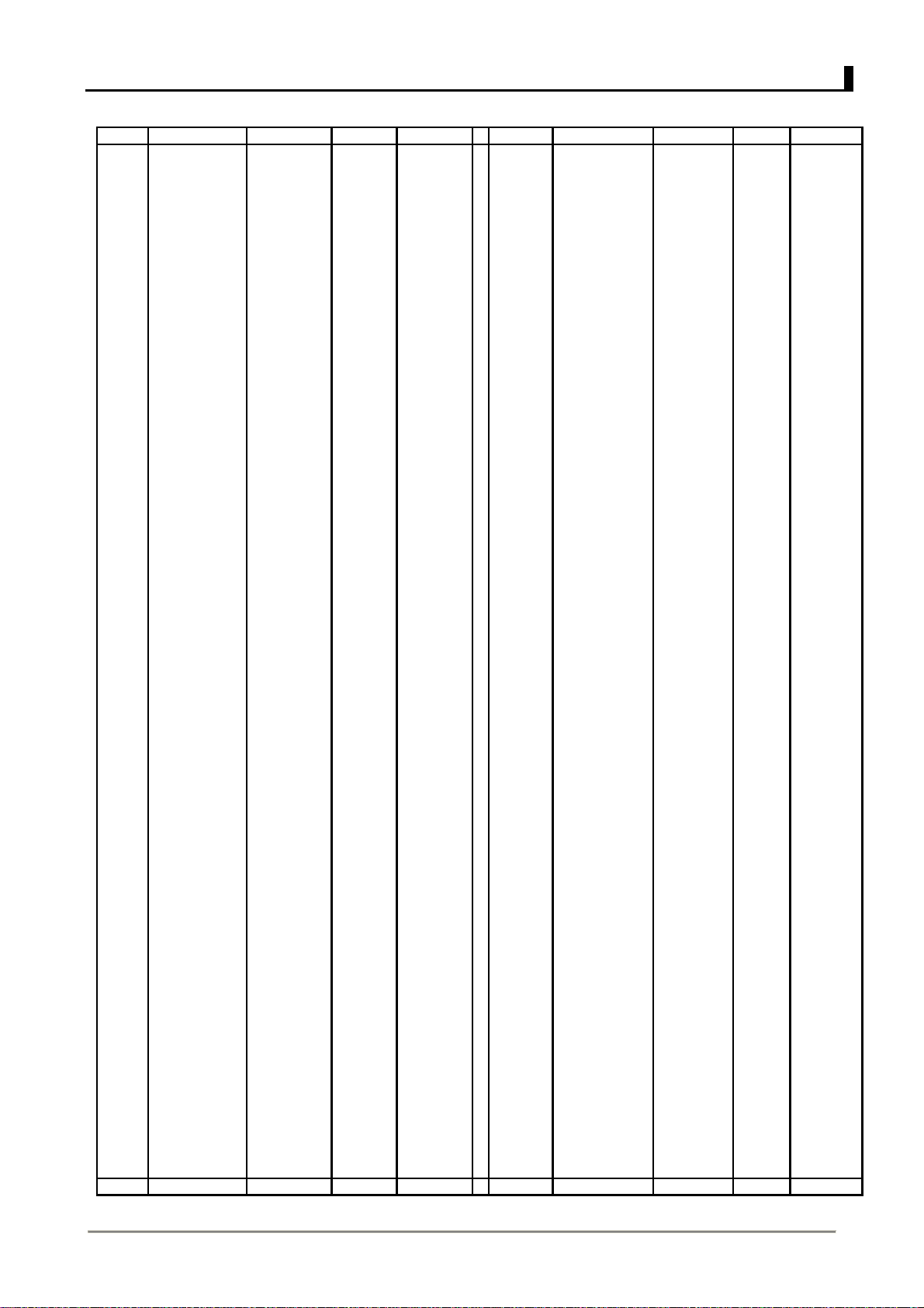
RPV516 Parts List
Ref. No. Material Code Description Address Destination Ref. No. Material Code Description Address Destination
R525 01031522 1.5K T4G C35 0203080B 8pF B1F
R526 01031531 15K T3G C35 0203060B 6pF B1F
R527 01031531 15K T3G C36 02031802 18pF B1F
R528 01037542 750K T4G C37 0203050B 5pF B2F
R529 01031832 18K T4G C38 02031802 18pF B1E
R530 01031012 100 T4H C39 02031033
R531 01030002 0 T2G C40 02031023 1000pF B1F
R532 01038212 820 T4H C41 02031023 1000pF B1E
R533 01031042 100K T4I C42 02031033
R534 01031822 1.8K T5H C43 02030R5B 0.5pF B2F
R535 01034712 470 T5H C44 02030R5B 0.5pF B2F
R536 01031022 1K T5J C45 02031023 1000pF B2F
R537 01031012 100 T5I C46 02031023 1000pF B2F
R538 01031012 100 T5H C47 02033302 33pF B2F
R539 01030002 0 T5H C48 02031000 10pF B2D
R540 01050002 0 T5B C49 02031023 1000pF B2F
R541 01034722 4.7K T5C C50 T0606475
R542 01030002 0 T3G C51 02036802 68pF B4C
R548 01033322 3.3K T2D C52 02031023 1000pF B2B
C53 02031043
C100 02031502 15pF B2F
CP1 014D102A 1K×4 B1C C101 02031023 1000pF B2F
C102 02031023 1000pF B2F
C103 02033302 33pF B3F
TH100 0140473B B3H C103 02032202 22pF B3F
TH500 0139222B T2C C104 02031023 1000pF B3F
C105 02031023 1000pF B3F
C106 02031023 1000pF B3G
VR1 0122683H T2C C107 02031023 1000pF B3G
VR500 0122683H T2D C108 0203120G 12pF B3F
VR501 0122153H T3E C109 02031023 1000pF B3G
C110 02031043
C111 02031023 1000pF B3G
C1 02031043
C2 02031012 100pF B1B C113 02032002 20pF B3G
C3 02031012 100pF B2B C114 02031023 1000pF B3G
C4 02031043
C5 T0606475
C6 02031012 100pF B1C C118 02031023 1000pF B3G
C7 02031023 1000pF B2C C119 02031023 1000pF B3H
C8 02052243
C9 02031000 10pF B2D C121 0206105Z
C10 02034702 47pF B3D C123 02031033
C12 02052243
C14 02031000 10pF B2D C125 02031043
C15 T0610685
C16 02036802 68pF B4D C127 T0610685
C17 02033313 330pF B3D C128 02031802 18pF B4I
C18 T0606684
C19 02031033
C20 02031033
C23 T0606106
C24 02036813 680pF B1D C131 02031023 1000pF B3I
C25 02034713 470pF B1C C132 02034713 470pF T1I
C26 02031212 120pF B4C C133 02031023 1000pF B4J
C27 02031023 1000pF B2B C134 02031012 100pF T1I
C28 02033302 33pF B4C C135 02033302 33pF B4I
C29 02031023 1000pF B2E C135 02032702 27pF B4I
C30 02031023 1000pF B2E C136 02034702 47pF B4I
C31 02031023 1000pF B1G C136 02033902 39pF B4I
C32 02031012 100pF B2E C137 02031023 1000pF B4I
C33 02033902 39pF B1G C138 0203120G 12pF B4J
0.1μF
0.1μF
4.7μF
0.22μF
0.22μF
6.8μF
0.68μF
0.01μF
0.01
μ
10μF
F
B1C C112 02031023 1000pF T2J
B2D C115 02031023 1000pF T3J
B2D C116 02031023 1000pF B3G
B1C C120 02031023 1000pF B3I
B1C C124 02031023 1000pF B3I
B1D C126 02035602 56pF B4I
B1D C128 02031502 15pF B4I
B3D C129 02031502 15pF B4I
B3D C129 0203090B 9pF B4I
B1B C130 02031023 1000pF T2H
0.01μF
0.01μF
4.7μF
0.1μF
0.1μF
1μF
0.01μF
0.1μF
6.8μF
- 22 -
B1E
B1F
B2G
B2B
B3G
B3J
B3I
B3I
T2G
Page 25
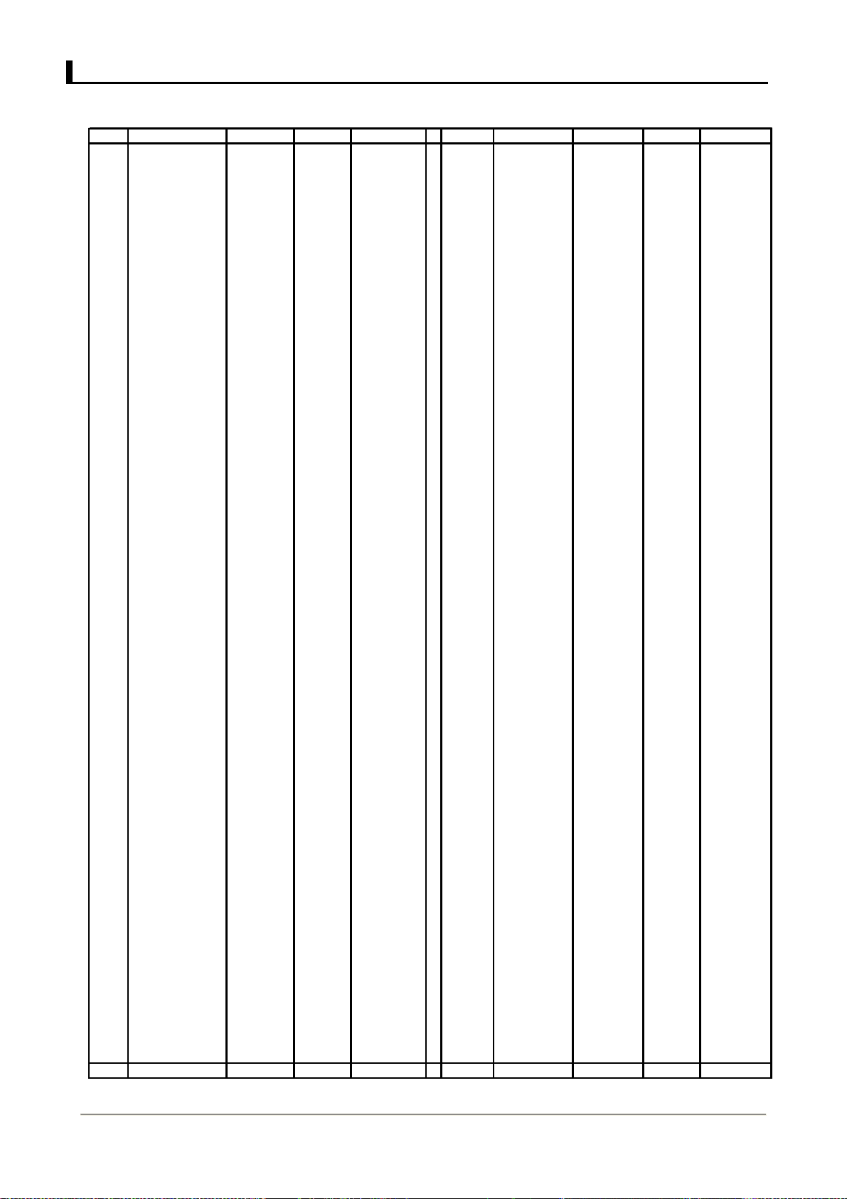
RPV516 Parts List
Ref. No.Material Code Description Address Destination Ref. No. Material Code Description Address Destination
C139 02031023 1000pF T2I
C255 02031602 16pF B4G
C140 0203080B 8pF B4J C256 02031023 1000pF B5B
C141 02034713 470pF T2I C257 02031R5B 1.5pF B4H
C142 02032202 22pF B4J
C143 0203080B 8pF B3I C259 02032002 20pF B4H
C144 0203080B 8pF B4J C260 02031023 1000pF B4H
C146 02032002 20pF B4J C261 0203120G 12pF B4H
C300 02038223 8200pF B2B
C147 0203080B 8pF B4K C301 02031833
C302 02031043
C200 T0606106
C201 02031033
C202 02031000 10pF B4B C305 02031033
C203 02034713 470pF B4B
C204 02034723 4700pF B4B C306 02034733
C205 02032212 220pF B4B C307 T0606106
C206 02032212 220pF B4B C308 02035623 5600pF B3A
C207 02031043
C208 02038202 82pF B5B C311 T0504225
C209 02031043
C210 02031033
C211 02031043
C212 02031502 15pF B5C C316 02031033
C213 02031043
C214 02031033
C215 02031000 10pF B4D C320 02033333
C216 0203020B 2pF B4D C321 02033333
C217 02031033
C218 02031023 1000pF B3E C327 02031043
C219 02031502 15pF B3E C330 02031012 100pF T1E
C220 02031023 1000pF B3E C331 02054743
C221 02031033
C222 0203060B 8pF B3E C333 0203474Z
C223 0203020B 2pF B5D C335 02034733
C224 02031043
C225 02031043
C233 0203060B 6pF B3E C338 02035602 56pF B4A
C234 02033002 30pF B3E C400 02031043
C235 02031043
C236 02031023 1000pF B3E C403 02031023 1000pF T2B
C237 0203060B 6pF B4E C404 02031023 1000pF T2B
C238 02032002 20pF B4E C406 02031023 1000pF B2K
C239 02031023 1000pF B4E C407 02031023 1000pF T4A
C241 0203050B 5pF B5G C409 0203030B 3pF T3B
C243 0203020B 2pF B4E C410 02031023 1000pF T4A
C245 02031023 1000pF B4F C411 02034713 470pF T2A
C246 02031023 1000pF B5E C412 02031000 10pF T3B
C247 02032002 20pF B5F C413 02031023 1000pF T3D
C248 0203080B 8pF B5E C415 02031000 10pF T3B
C249 02031023 1000pF B5E C416 02031023 1000pF T5A
C250 02031023 1000pF B5F C417 0206105Z
C251 02031023 1000pF B4F C418 02031033
C252 02031802 18pF B4F C421 02031033
C253 02031023 1000pF B4E C422 02031033
C254 02031R5B 1.5pF B4G
10μF
0.01μF
0.1μF
0.1μF
0.01μF
0.1μF
0.1μF
0.01μF
0.01μF
0.01μF
0.1μF
0.1μF
0.1μF
B4B C303 02031043
B4B C304 T0606106
B4B C309 02031033
B5B C312 02031033
B5B C313 02051053
B5B C314 02031023 1000pF B4A
B5B C318 02033333
B5C C319 02034733
B4E C322 02051043
B4D C332 T0606106
C334 02032212 220pF T2F
B5D C336 02031033
B5B C337 T2006107
B3E C402 02031023 1000pF B2K
C408 T0606106
C414 02031023 1000pF T5B
C420 02031033
0.018μF
0.1μF
0.1μF
10μF
0.01μF
0.047μF
10μF
0.01μF
2.2μF
0.01μF
1μ F
0.01μF
0.033μ
0.047μF
0.033μF
0.033μF
0.1μF
0.1μF
0.47μF
10μF
0.47μF
0.047μF
0.01μF
100μF
0.1μF
10μF
1μ F
0.01μF
0.01μF
0.01μF
0.01μF
B3B
B1B
B3B
B3A
B2B
B2B
B2A
B1B
B4A
B1B
B3B
B1B
B4B
F
B4A
B1A
B1A
B1A
T2E
T2E
T1E
T1E
T2F
T1F
T2G
T2B
T4A
T5A
T4K
T4K
B2I
T4J
- 23 -
Page 26
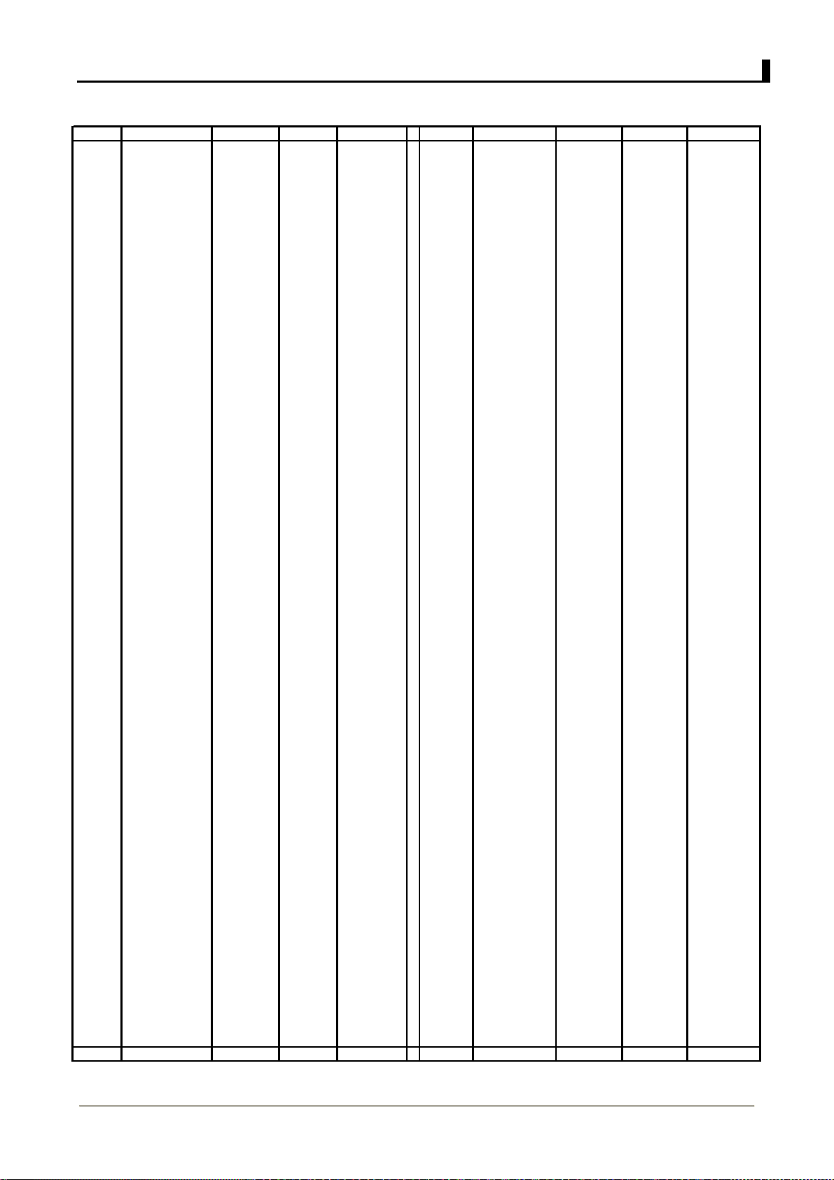
RPV516 Parts List
Ref. No. Material Code Description Address Destination Ref. No. Material Code Description Address Destination
C423 02031033 1000pF B2H L17 03202210 220nH B4C
C424 02051053
C425 02031033
C427 02031023 1000pF B2H L101 03186800 68nH B3G
C429 02051053
C430 02051053
C500 02032733
C501 02032733
C502 02033923 3900pF T5C L107 03023300 33nH B3H
C503 02033333
C504 T0606475
C505 02051053
C506 02034713 470pF T3G L112 03083220
C507 T0504225
C508 02031033
C509 02033323 3300pF T3E L115 03193560 6T B4J
C510 02038213 820pF T3E L117 03193550 5T B4J
C511 02034733
C512 02033323 3300pF T3F L200 03085610
C513 02036813 680pF T3F L201 03088210
C514 02034733
C515 02031033
C516 02031000 10pF T3F L203 03215600 56nH B5E
C517 02031023 1000pF T3F L204 03087510 0.75uH B4E
C518 02032233
C519 T0606475
C520 02032233
C521 02031023 1000pF T4G L209 03215600 56nH B4G
C522 02051043
C523 T0504225
C524 02032733
C525 02031043
C526 02034713 470pF T4H L214 03215600 56nH B4E
C527 T0606106
C528 02031023 1000pF B2J L400 03182210
C529 02051023 1000pF T5I L401 0312601S T4B
C530 02032212 220pF T5J L402 03182210
C531 02032212 220pF T5I L403 03182210
C532 02034713 470pF B5H L500 0312602S T4I
C533 02031043
1μF
0.01μF
1μ F
1μ F
0.027μ F
0.027μ F
0.033μ F
4.7μF
1μ F
2.2μF
0.01μF
0.047μ F
0.047μF
0.01μF
0.022μ
4.7μF
0.022μ F
0.1μF
2.2μF
0.027μ F
0.1μF
10μ F
0.1μF
B2J
T4J L100 03188200 82nH B2G
B3H L102 0312601S B3F
B2J L103 03182700 27nH B3G
T2C L104 03081020
T2C L105 0313221S B3H
L108 03193550 5T B3I
T5C L109 0313600S B3I
T2B L110 03190530 3T B3I
T3E L111 03193540 4T B4I
T3E L113 03193570 7T B4I
T3E L114 03193550 5T B4J
T3F L118 03021020
T3F L202 03202210 220nH B3E
T3E
T4G
F
T3G L208 03215600 56nH B4G
T4G
T4G
T5H L210 03214700 47nH B4H
T4G L211 03183300 33nH B4F
T4I
T5H L215 03085610
T2C L501 0313221S B2J
L502 0313221S T5I
1μ H
2.2μH
1μ H
0.56μH
0.82μH
0.56μH
0.22μH
0.22μH
0.22μH
B3H
B4J
T2J
B3E
B3E
B3E
T3D
T3D
T3B
TC1 022Z06A0 10pF B1E
TC2 022Z06A0 6pF B1G IC1 071511P0 B2C
TC201 022Z10A0 10pF B4G IC100 072904V0 T2I
IC200 07311360 B4B
IC300 072902V0 B2A
L1 0312601S B2D IC301 072904V0 B4A
L2 03081020
L4 03184710
L5 03185610
L6 03066820
L7 0312601S B1D
L8 03066820
L9 03066820
L10 03032300 23nH B1F
L11 03033300 33nH B2E Q1 05025108 B3D
L12 03181010 100nH B2F Q2 05025108 B2D
L13 03184700 47nH B2E Q3 06011875 B1F
L14 0312601S B1E Q4 06011875 B2E
L15 03066820
L16 03202210 220nH B4C Q6 05025108 B2F
1μH
0.47μH
0.56μH
6.8μH
6.8μH
6.8μH
6.8μH
B2D IC302 077368F0 T2E
B3D IC400 079140NR T2B
B3D IC401 0724C080 T5B
B2E IC402 075VL45C T2B
IC403 07380342 T3C
B2E IC404 0781350H T5A
B1G IC500 072100V0 T3G
B1G Q5 06002430 B1E
- 24 -
Page 27
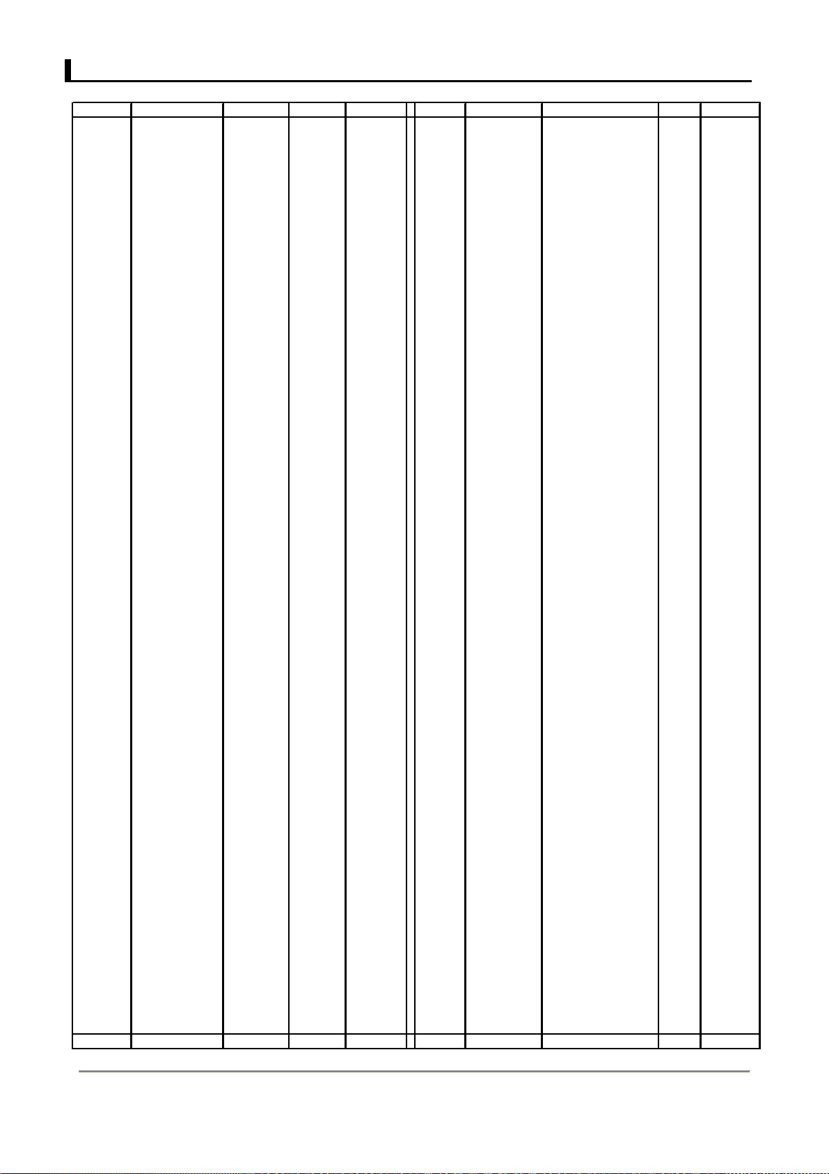
RPV516 Parts List
Ref. No. Material Code Description Address D estination Ref. No. M aterial Code Description A ddress Destination
Q7 0508UMC4 B1F X400 10073728 7.3728MHz T3A
Q8 05024617 B2F
Q100 05025108 B2F
Q101 05024988 B3G XF200 11388500 38.85MHz B4D
Q102 06013475 B3G
Q103 06011824 T2J
Q104 05107170 T2J CF200 1145000F 450kHz B4C
Q105 06013476 B3H
Q106 06011824 T2H
Q107 0506114T T2H CD200 12450001 450kHz B5A
Q108 0506114E T2G
Q109 0506144E T2H
Q200 0505114E B5B F500 0903A32V 3.0A/32V T5J
Q201 05024649 B5C
Q202 06023200 B3E
Q203 06023200 B4F S402 19060020 SKHLLB B5I
Q300 05024617 B1B S403 19060020 SKHLLB B5G
Q302 06011824 B1A
Q303 0505144E B2A
Q304 0506144E T1D MIC500 13090010 WM-54BT T1H
Q305 05001362 T2E
Q306 0506144E T1F
Q307 06011588 T2F SP 13090020
Q400 0506114E B2K
Q401 0506114E B2K
Q402 0505114Y T4B J500 08021030 B1I
Q403 0506144E T3B J501 08021010 B1H
Q404 0508UMG3 B2I
Q405 0509672T B2H VR401 19090010 B1K
Q406A 05105910 B2I
Q406B 05105910 B2I S401 19090030 B3K
Q407 0508UMG3 B2I
Q408 0505123J B2J CN100
Q500 06011824 T3G CN500
Q501 05024617 T3E W 500 20020801
Q502 05024617 T3F W 501 20020800
Q503 05024919 T4H
Q504 0505143Z T4C
D1 04012830 B2E
D2 04012830 B2E
D3 04012830 B1G
D4 04012830 B1G
D5 04022140 B1E
D6 04072S11 B2F
D7 04072S11 B1C
D8 04103R00 B2B
D100 0407S077 B3F
D101 04077700 B4I
D102 0407S077 B4I
D103 0407S077 B4I
D200 0407S077 B3F
D201 0411350B B4E
D202 0411350B B5F
D203 0411350B B4F
D204 0411350B B4H
D205 0411350B B4H
D400 0402190R T4K
D401 0402190G T4K
D500 04003720 T4G
D501 04032220 T4H
D502 04151540 B2K
R600 01034732 47K T1A
R601 01031032 10K T2A
R602 01036842 680K T1A
R603 01031032 10K T2A
R604 01035621 5.6K T2A
R605 01031032 10K T2A
R606 01034732 47K T2B
R607 01033932 39K T2B
R608 01031022 1K T1A
R701 01031032 10K T4H
R702 01031032 10K T4H
R703 01031022 1K T4I
C600 02031043 0.1u T1B
C601 T0616475 4.7uF T2A
C602 02031023 1000p T2A
C603 02031043 0.1u T2A
C604 02031233 0.012u T2A
C605 02031012 10 0p T1A
C606 02031233 0.012u T2A
C701 02033923 3900p T4H
C702 02033333 0.033u T4H
C703 02031033 0.01uF T4I
C704 02036823 6800p T4H
C54 02031043 0.1u T2C
4Ω 0.5W
antenna socket
power electrode
wire ASTVR1 Φ0.35red
wire ASTVR1 Φ0.35black
T1K
B2J
T5I
T5I
X1 10128CXO 12.8MHz B3C
- 25 -
IC 8
077501FU
T1B
Page 28
RPU416 Parts List
RPU416 Parts List
Ref. No. Material code Description Address Destin ation Ref. No. Material code Descri ption Address Destination
1 1509103A f ront cov er R27 01033312 330 B1F
2 1509105A bezel (ptt) R 28 01032202 22 B1F
3 1609205A button(ptt) R 29 01030002 0 B2C
4 1409302A
5 1509106A knob(enc) R 31 01031012 100 B2F
6 1509107A knob(v ol) R32 01034722 4.7K B2F
7 14013110 inner liner(knob) R33 01031022 1K B1F
8 14013190
9 1509102A panel(top) R 35 01033312 330 B2B
10 1509104A water-resistant c ap (SPK/MIC ) R100 01033322 3.3K B2E
11 14063080 spring(battery release) R101 01035621 5.6K B2E
12 14063090 metal piece(battery release) R 102 01032712 270 B2E
13 15061090 latch (battery release) R103 01033322 3.3K B2E
14 1609203S speaker washer R104 01031002 10 B2F
15 13090020 speaker R 105 01033322 3.3K B2E
16 16092020 MIC washer R106 01033322 3.3K B3F
17 1609206S
18 14063101
19 1609207S shroud(SP/MIC plug) R109 01032202 22 B3F
20 15061140
21 16094050 washer (holder) R111 01032202 22 B3G
22 14093100 socket (antenna) R 112 01031522 1.5K B3F
23 1409309S
24 14063071 cathode piece(battery ) R 115 01031002 10 B3F
25 19090041 battery R 117 01034732 47K B3G
26 14093060 spring(belt clip) R117 01031242 120K B3G
27 15091050 holder(belt clip) R118 01034732 47K B3G
28 15091040 belt clip R 119 01034722 4.7K T2J
29 14093050 pin R120 01030002 0 B3G
R1 01031022 1K T5C R 122 01036812 680 T2J
R2 01031022 1K B1C R123 01050002 0 B4I
R3 01031002 10 B2D R124 01036812 680 T2J
R4 01031022 1K B3D R125 01031832 18K B3G
R5 01035612 560 B1C R 125 01034732 47K B3G
R6 01031541 150K B1C R126 01034732 47K B3H
R7 01035612 560 B1C R 127 01030002 0 B3H
R8 01033342 330K B3D R128 01034702 47 B3H
R9 01032722 2.7K B1C R 130 01050002 0.5 T2J
R10 01032222 2.2K B1D R 131 01050002 0.5 T2J
R11 01034732 47K B3B R132 01050002 0.5 T2J
R12 01033932 39K B3B R133 01031541 150K T1I
R13 01030002 0 B1D R134 01031541 150K T1I
R14 01031012 100 B3D R 135 01031541 150K T1I
R15 01031032 10K B1D R136 01031541 150K T1I
R16 01034732 47K B2E R137 01031541 150K T1I
R18 01031042 100K B2E R138 01031541 150K T1I
R19 01031012 100 B2E R139 01032712 270 B4J
R20 01031022 1K B2D R140 01031032 10K T2I
R21 01031042 100K B2D R141 01034732 47K T1I
R22 01034732 47K B1E R142 01031052 1M T2I
R23 01033922 3.9K B1E
R23 01036822 6.8K B1E
R24 01034722 4.7K B1E
R24 01038222 8.2K B1E
R25 01031512 150 B1F
R25 01031012 100 B1F
R26 01031012 100 B1F R153 01033322 3.3K T2H
R27 01032712 270 B1F
nut (antenna base)
nut (switc h)
water-resis tant ring
anode connector(battery )
holder(anode piece)
aluminum chassis
RPU416B
RPU416A
RPU416B
RPU416A
RPU416B
RPU416A
RPU416B
R30 01031241 120K B2F
R34 01031042 100K B1F
R107 01034732 47K B3F
R108 01033312 330 B3F
R110 01036812 680 B3F
R113 01033312 330 B3G
R121 01034702 47 B3G
R143 01030002 0 T1H
R144 01032222 2.2K T2H
R145 01031842 180K T1I
R146 01031042 100K T1H
R147 01030002 0 B4I
R152 01033912 390 T2H
R154 01032712 270 B4J
RPU416A
RPU416B
RPU416A
RPU416B
RPU416A
RPU416A
- 26 -
Page 29
RPU416 Parts List
Ref. No. Material code Description Address Destination Ref. No. Material code Description Address Destination
R200 01031002 10 B5C R330 01034732 47K T2D
R201 01033922 3.9K B3B R331 01032222 2.2K T1E
R202 01031842 180K B4B R332 01031512 150 T1E
R203 01033322 3.3K B4B R333 01034741 470K T1F
R204 01033322 3.3K B4B R334 01031002 10 T2F
R205 01038212 820 B5B R335 01035632 56K T2F
R206 01031842 180K B4B R336 01033332 33K T2F
R207 01031042 100K B5B R338 01034732 47K B2A
R208 01036842 680K B5C R339 01038222 8.2K T1D
R209 01032722 2.7K B5C R340 01031241 120K B1B
R210 01034712 470 B5C R341 01031042 100K T1F
R211 01034712 470 B3E R342 01034722 4.7K T4C
R212 01034702 47 B3E R400 01033342 330K T2B
R213 01030002 0 B3E R401 01031042 100K T4C
R214 01031032 10K B3E R402 01032212 220 B2K
R215 01032212 220 B3E R403 01031812 180 B2K
R216 01034722 4.7K B3E
R216 01031222 2.2K B3E
R217 01030002 0 B3E R406 01032222 2.2K B2J
R218 01031012 100 B5E R407 01031022 1K T2A
R219 01033322 3.3K B5E R408 01031042 100K T2A
R220 01031512 150 B5F
R220 01032212 220 B5F
R221 01032241 220K B4E R411 01032241 220K T2A
R222 01031022 1K B3E R412 01031002 10 T3B
R223 01031042 100K B4E R413 01031022 1K T2D
R224 01030002 0 B4F R414 01034732 47K T4K
R225 01030002 0 B5F R415 01034732 47K T4K
R226 01032222 2.2K B3E R416 01034722 4.7K T4C
R227 01030002 0 B5H R417 01031002 10 T4K
R228 01031042 100K B5E R418 01032222 2.2K T2C
R230 01031042 100K B4E R419 01030002 0 B2I
R231 01031042 100K B4G R420 01031022 1K B2I
R232 01031042 100K B4H
R233 01030002 0 B3E R422 01032722 2.7K B2H
R300 01039131 91K B1B R423 01034732 47K T4J
R301 01035621 5.6K B3B R424 01033322 3.3K B2I
R302 01035621 5.6K B3B R425 01033322 3.3K B2I
R303 01033322 3.3K B3B R426 01038222 8.2K B2K
R304 01031052 1M B3B R427 01031022 1K B2H
R305 01031832 18K B2A R428 01032722 2.7K B2H
R306 01031241 120K B3A R429 01038212 820 B2H
R307 01034732 47K B2A R430 01031012 100 T4J
R308 01031032 10K B3A R431 01030002 0 T4J
R309 01034741 470K B3B R432 01031032 10K B2H
R310 01050002 0 T1F R433 01031531 15K B2H
R311 01050002 0 B3A R434 01031531 15K B1H
R312 01031232 12K B2B R435 01031032 10K B2H
R313 01031032 10K B3A
R314 01034741 470K B2A R501 01034722 4.7K T2C
R315 01033941 390K B2A R502 01038232 82K T5C
R316 01032741 270K B3A R503 01034732 47K T2D
R317 01032741 270K B2B R503 01036832 68K T2D
R318 01031842 180K B4A R504 01036832 68K T2D
R320 01034732 47K B3B R504 01033332 33K T2D
R321 01032232 22K B1B R505 01031241 120K T2D
R322 01032241 220K B2A R505 01031541 150K T2D
R323 01031042 100K B4A R506 01031032 10K T3E
R324 01035621 5.6K B1B R506 01032232 22K T3E
R325 01031042 100K B4A R507 01034732 47K T3E
R326 01035621 5.6K B1A R508 01035621 5.6K T3E
R327 01030002 0 T2E R509 01031241 120K T2C
R328 01031022 1K B1A R510 01033322 3.3K T3E
R329 01030002 0 B2A R511 01031032 10K T3F
RPU416B
RPU416A
RPU416B
RPU416A
RPU416B
- 27 -
R404 01030002 0 T2B
R405 01031022 1K T4B
R409 01031022 1K T3B
R410 01038222 8.2K B2K
R421 01034732 47K T4J
R500 01034722 4.7K T2C
RPU416B
RPU416A
RPU416B
RPU416A
RPU416B
RPU416A
RPU416B
RPU416A
Page 30
RPU416 Parts List
Ref. No. Material code Description Address Destination Ref. No. Material code Description Address Destination
R512 01031852 1.8M T3E C18 02031043
R513 01034732 47K T2C
R513 01033332 33K T2C
R514 01033332 33K T3E C23 T0606106
R515 01033332 33K T3F C24 02031033
R516 01031032 10K T3F C25 02034713 470pF B1D
R517 01031852 1.8M T3F C26 02031212 120pF B4C
R518 01031032 10K T2C
R518 01036822 6.8K T2C
R519 01033332 33K T3F C29 0203020B 2pF B1D
R520 01033332 33K T3F C30 02031023 1000pF B1F
R521 01033322 3.3K T3F C31 02031012 100pF B2E
R522 01031822 1.8K T3F C34 02031802 18pF B1G
R523 01036822 6.8K T3F C35 0203080B 8pF B2E
R524 01035132 51K T3F C35 0203070B 7pF B2E
R525 01031522 1.5K T4G C36 0203070B 7pF B1E
R526 01031531 15K T3G C36 0203080B 8pF B1E
R527 01031531 15K T3G C37 02033002 30pF B1G
R528 01037542 750K T4G C37 02033302 33pF B1G
R529 01031832 18K T4G C38 0203060B 6pF B1G
R530 01031012 100 T4H C38 0203050B 5pF B1G
R531 01030002 0 T2G C39 02031000 10pF B2F
R532 01038212 820 T4H C39 0203080B 8pF B2F
R533 01031042 100K T4I C40 02030R5B 0.5pF B1E
R534 01031822 1.8K T5H C41 0203050B 5pF B1E
R535 01034712 470 T5H C41 0203040B 4pF B1E
R536 01031022 1K T5J C42 0203120G 12pF B2F
R537 01031012 100 T5I C42 02031000 10pF B2F
R538 01031012 100 T5H C43 02031023 1000pF B1F
R539 01030002 0 T5H C44 0203070B 7pF B1F
R540 01050002 0 T5B C44 0203040B 4pF B1F
R541 01034722 4.7K T5C C45 02031000 10pF B1F
R542 01030002 0 T3G C45 0203080B 8pF B1F
R543 01030002 0 T3E C46 02034713 470pF B1E
R548 01033322 3.3K T2D C47 0203010B 1pF B2F
CP1 014D102A 1K×4 B1C C51 02036802 68pF B4C
TH102 0140473B 47K B3H C54 0203030B 3pF B2D
TH500 0139222B 2.2K T2C C55 02034713 470pF B2F
TH501 0139222B 2.2K T3E C56 T0606475
VR1 0122683H 68K T2C C100 02032202 22pF B2E
VR500 0122473H 47K T2D C101 02034713 470pF B2E
VR501 0122473H 47K T3E C102 02034713 470pF B2F
C1 02031043
C2 02031012 100pF B1B C106 02034713 470pF B3F
C3 02031012 100pF B2B C107 02034713 470pF B3F
C4 02031043
C5 T0606475
C6 02031012 100pF B1C C110 02034713 470pF B3G
C7 02034713 470pF B2C C111 0203060B 6pF B3F
C9 02031000 10pF B2D C112 02034713 470pF T2J
C10 02034702 47pF B3D C113 02031043
C12 02031043
C14 02031000 10pF B2D C115 02034713 470pF T3J
C15 T1616105
C16 02036802 68pF B4D C118 02032702 27pF B3G
C17 02033313 330pF B3D C119 02031023 1000pF B3G
0.1
μF
0.1μF
4.7μF
0.1μF
1μF
B1C C105 0203060B 6pF B2E
B2D C108 0203070B 7pF B3F
B2D C109 02034713 470pF B3G
B1C C114 02034713 470pF B3G
B1D C116 02031023 1000pF B3G
RPU416B
RPU416A
RPU416B
RPU416A
C19 02031033
C20 02031033
C27 02034713 470pF B2B
C28 02033302 33pF B4C
C48 02034713 470pF B1F
C49 02030R5B 0.5pF B1F
C52 02034713 470pF B2F
C53 0203060B 6pF B2F
C57 02034713 470pF B2B
C58 02031043
C103 02034713 470pF B2E
C104 02031043
0.1μF
0.01μF
0.01μF
10μF
0.01μF
4.7μF
0.1μF
0.1μF
0.1μF
B1D
B3D
B3D
B2B
B2E
RPU416B
RPU416A
RPU416B
RPU416A
RPU416B
RPU416A
RPU416B
RPU416A
RPU416B
RPU416A
RPU416B
RPU416A
RPU416B
RPU416A
RPU416B
RPU416A
RPU416B
RPU416A
B2F
B3B
B2F
B3G
- 28 -
Page 31
RPU416 Parts List
Ref. No. Material code Description Address Destination Ref. No. Material code Description Address Destination
C120 02034713 470pF B3G C222 0203050B 5pF B3E
C121 02034713 470pF B3G C223 0203020B 2pF B5D
C123 02031023 1000pF B3H C224 02034713 470pF B3E
C125 02034713 470pF B3I C226 02030R5B 0.5pF B5E
C126 02051053
C127 T0610685
C128 02031033
C129 02034713 470pF B3I C229 02034713 470pF B5E
C130 02052202 22pF B4I C231 02034713 470pF B5F
C131 02031043
C132 02034713 470pF T1I C233 02030R3B 0.3pF B4G
C134 02031012 100pF T1I C234 02030R3B 0.3pF B5H
C135 0203010B 1pF B4I C235 02035R6B 5.6pF B5H
C136 0203070B 7pF B4I
C136 0203080B 8pF B4I
C138 02034713 470pF B4I
C138 02031013 100pF B4I
C139 02034713 470pF T2I C238 02030R5B 0.5pF B4E
C140 0203010B 1pF B4I
C141 02034713 470pF T2I C239 0203040B 4pF B4E
C142 0203050B 5pF B4I
C142 0203030B 3pF B4I
C143 02034713 470pF B4J C252 0203070B 7pF B4F
C144 0203020B 2pF B4I C252 02034R7B 4.7pF B4F
C145 02034713 470pF B4J C253 02034713 470pF B4E
C147 02031R5B 1.5pF B5J
C147 0203010B 1pF B5J
C148 0203010B 1pF B5J
C149 0203010B 1pF B4J C256 02031043
C150 0203040B 4pF B4J
C150 0203050B 5pF B4J
C151 0203020B 2pF B4J
C151 02031R5B 1.5pF B4J
C153 0203040B 4pF B4J
C153 0203030B 3pF B4J
C154 0203020B 2pF B4K
C154 0203010B 1pF B4K
C155 02031R5B 1.5pF B4K
C156 02031043
C157 02034713 470pF B3F C303 02031043
C165 02034713 470pF T2H C304 T0606106
C200 T0606106
C201 02031033
C202 02031000 10pF B4B C307 T0606106
C203 02034713 470pF B4B C308 02035623 5600pF B3A
C204 02034723 4700pF B4B C309 02031033
C205 02032212 220pF B4B C311 T0610225
C206 02032212 220pF B4B C312 02031033
C207 02031043
C208 02038202 82pF B5B C314 02031023 1000pF B4A
C209 02031043
C210 02031033
C211 02031043
C212 02033302 33pF B5C C321 02033333
C213 02031043
C214 02031033
C215 02031302 13pF B4D C330 02031012 100pF T1E
C217 02031033
C218 02034713 470pF B3E C332 T0606106
C219 0203150G 15pF B3E C333 02034743
C220 02031033
C221 02031033
C222 0203060B 6pF B3E
1μF
6.8μF
0.01μF
0.1μF
0.1μF
10μF
0.01μF
0.1μF
0.1μF
0.01μF
0.1μF
0.1μF
0.01μF
0.01μF
0.01μF
0.01μF
B3J C227 0203150G 15pF B5E
T2G C227 02031000 10pF B5E
B3I C228 0203080B 8pF B5E
B3I C232 02034713 470pF B4E
RPU416B
RPU416A
RPU416B
RPU416A
RPU416B
RPU416B
RPU416A
RPU416B
RPU416A
RPU416A
RPU416B
RPU416A
RPU416B
RPU416A
RPU416B
RPU416A
RPU416B
RPU416A
RPU416A
B3F C302 02031043
B4B C305 02031033
B4B C306 02034733
B4B C313 02051053
B5B C316 02031033
B5C C318 02033333
B5B C320 02033333
B5B C322 02051043
B5C C327 02031043
B4E C331 02054743
B4E C334 02032212 220pF T2F
B4D C335 02034733
RPU416B
C235 0203030B 3pF B5H
C236 0203010B 1pF B4H
C236 0203030B 3pF B4H
C237 02034713 470pF B4E
C239 0203070B 7pF B4E
C241 02031R5B 1.5pF B3E
C241 0203060B 6pF B3E
C254 02034713 470pF B4G
C255 0203060B 6pF B4G
C255 02033R6B 3.6pF B4G
0.1μF
C257 02034713 470pF B5E
C258 02031043
C259 0203070B 7pF B5E
C259 0203040B 4pF B5E
C260 0203030B 3pF B4H
C261 0203040B 4pF B5H
C300 02038223 8200pF B3B
C301 02031833
C319 02034733
C336 02031033
0.1μF
0.018μF
0.1μF
0.1μF
10μF
0.01μF
0.047μF
10μF
0.01μF
2.2μF
0.01μF
1μF
0.01μF
0.033μF
0.047μF
0.033μF
0.033μF
0.1μF
0.1μF
0.47μF
10μF
0.47μF
0.047μF
0.01μF
B5B
B5D
B3B
B1B
B3B
B3A
B2B
B2B
B2A
B1B
B4A
B1B
B3B
B1B
B4B
B4A
B1A
B1A
B1A
T2E
T2E
T1E
T1E
T2F
T1F
RPU416A
RPU416B
RPU416A
RPU416B
RPU416A
RPU416B
RPU416A
RPU416B
RPU416A
RPU416B
RPU416A
RPU416B
RPU416A
RPU416B
RPU416A
RPU416B
RPU416A
RPU416B
- 29 -
Page 32
RPU416 Parts List
Ref. No. Material code Description A ddress Destination R ef. No. Material code Description Address D estination
C337 T2006107
C338 02035602 56pF B4A TC2 022Z10A 0 10pF B1G
C400 02031043
C402 02034713 470pF B2K T C202 022Z06A0 6pF B4F
C403 02034713 470pF T2B TC203 022Z06A0 6pF B4G
C404 02034713 470pF T2B
C406 02034713 470pF B2K
C407 02031023 1000pF T4A L1 0312601S B2D
C408 T0606106
C409 0203030B 3pF T3B L4 03184710
C410 02034713 470pF T4A L5 03185610
C411 02034713 470pF T2A L6 03181800 18nH B1D
C412 02031000 10pF T3B L7 0312601S B2D
C413 02031023 1000pF T3D L8 03181010 100nH B1F
C414 02034713 470pF T5B L9 03063320
C415 02031000 10pF T3B L10 0312601S B 1E
C416 02034713 470pF T5A L11 03063320
C417 0206105Z
C418 02031033
C420 02031033
C421 02031033
C422 02031033
C423 02033333
C424 02051053
C425 02031033
C427 02034713 470pF B2H L18 03184700 47nH B4C
C429 02051053
C430 02051053
C500 02032733
C501 02032733
C502 02033923 3900pF T5C L101 03181800 18nH B3F
C503 02033333
C504 T0606475
C505 02051053
C506 02034713 470pF T3G L105 0313221S B3H
C507 T0504225
C508 02031033
C509 02033323 3300pF T3E L109 03202210 220nH B4J
C510 02036812 680pF T3E L110 03193540 4T B4I
C511 02034733
C512 02033323 3300pF T 3F L113 03193550 5T B4J
C513 02036812 680pF T 3F L113 03193540 4T B4J
C514 02034733
C515 02031033
C516 02031000 10pF T3F L118 03021020
C517 02034713 470pF T 3F L119 03183N3S 3.3nH B3G
C518 02032233
C519 T0606475
C520 02032233
C521 02031023 1000pF T4G L201 03085610
C522 02051043
C523 T0504225
C524 02032733
C525 02031043
C526 02034713 470pF T4H L207 03183900 39nH B5F
C527 T0606106
C528 02034713 470pF B2J L209 03193530 3T B4G
C529 02054713 470pF T5I L210 03193530 3T B5H
C530 02032212 220pF T5J L211 03193530 3T B4H
C531 02032212 220pF T5I L214 03193530 3T B4E
C532 02034713 470pF B5H L400 03182210
TC1 022Z10A0 10pF B1E
100μF
0.1μF
10μF
1μF
0.01μF
0.01μF
0.01μF
0.01μF
0.033μF
1μF
0.01μF
1μF
1μF
0.027μF
0.027μF
0.033μF
4.7μF
1μF
2.2μF
0.01μF
0.047μF
0.047μF
0.01μF
0.022μF
4.7μF
0.022μF
0.1μF
2.2μF
0.027μF
0.1μF
10μF
T2G TC1 022Z06A0 6pF B1E
T2B TC 201 022Z06A0 6pF B5E
T4A L2 03081020
T5B L12 03181010 100nH B1G
T4K L13 03032700 27nH B1G
T4K L13 03032300 23nH B1G
B2I L14 03032700 27nH B 1E
T4J L14 03032300 23nH B1E
B2H L15 03181010 100nH B2F
B2J L16 03202210 220nH B 4C
T4J L17 03202210 220nH B 4C
B3H L19 0312601S B 2F
B2J L20 03063320
T2C L21 03182200 22nH B 2F
T2C L100 03182200 22nH B2E
T5C L102 03181500 15nH B3G
T2B L103 0312601S B3F
T3E L104 03081020
T3E L106 03193580 8T B3I
T3E L107 0313600S B3I
T3F L112 03193540 4T B4J
T3F L114 03193540 4T B4J
T3E L114 03193530 3T B4J
T4G L119 03182N2S 2.2nH B3G
T3G L120 03222N7S 2.7nH B3H
T4G L200 03083310
T4G L202 03182200 22nH B3E
T5H L203 03193530 3T B5E
T4G L204 03193530 3T B 5E
T4I L206 03181800 18nH B5E
T5H L208 03193530 3T B4F
L401 0312601S T4B
L402 03182210
RPU416B
L403 03182210
1μH
0.47μH
0.56μH
3.3μH
3.3μH
3.3μH
1μH
1μH
0.33μH
0.56μH
0.22μH
0.22μH
0.22μH
B2D
B3D
B3D
B2E
B2E
B2F
B3H
T2J
B3E
B3E
T3D
T3D
T3B
RPU416A
RPU416B
RPU416A
RPU416B
RPU416A
RPU416A
RPU416B
RPU416A
RPU416B
RPU416A
RPU416B
RPU416A
RPU416B
- 30 -
Page 33
RPU416 Parts List
Ref. No. Material code Description Address Destination Ref. No. Material code Description Address Destination
L500 0312601S T4I D1 04072376 B1F
L501 0313221S B2J D2 04072376 B2E
L502 0313221S T5I D3 04072376 B1F
D4 04072376 B2E
D5 04022140 B1E
IC1 071511P0 B2C D5 04073600 B1E
IC100 072904V0 T2I D6 04072S11 B2F
IC200 07311360 B4B D7 04072S11 B1C
IC300 072902V0 B2A D8 04103R00 B2B
IC301 072904V0 B4A D100 0407S077 B3E
IC302 077368F0 T2E D101 04077700 B4J
IC400 079140NR T2B D102 0407S077 B4I
IC401 0724C080 T5B D103 0407S077 B4I
IC402 075VL45C T2B D200 0407S077 B3E
IC403 07380342 T3C
IC404 0781350H T5A D202 0411350B B4G
IC500 072100V0 T3G D203 0411350B B5E
Q1 05025108 B3D D401 0402190G T4K
Q2 05025108 B2D D500 04003720 T4G
Q3 05045080 B1G D501 04032220 T4H
Q4 05024226 B1F D502 04151540 B2K
Q5 06002430 B1F
Q6 05025108 B2F
Q7 0508UMC4 B1F X1 10128CXO 12.8MHz B3C
Q8 05024617 B2F
Q100 05025108 B2E
Q101 05025108 B3F X400 10073728 7.3728MHz T3A
Q102 05024988 B3G
Q103 06011824 T2J
Q104 05107170 T2J XF201 11388500 38.85MHz B4D
Q105 06013475 B3G
Q106 06011824 T2H
Q107 06013476 B3H CF200 1145000F 450kHz B4C
Q108 0506114E T2G
Q109 0506144E T2H
Q110 0506114T T2H CD200 12450001 450kHz B5A
Q200 0505114E B5B
Q201 05024649 B5C
Q202 06023200 B3E F500 0903A32V 3.0A/32V T5J
Q203 06023200 B4F
Q300 05024617 B1B
Q302 06011824 B1A S402 19060020 SKHLLB B5I
Q303 0505144E B2A S403 19060020 SKHLLB B5G
Q304 0506144E T1D
Q305 05001362 T2E MIC500 13090010 T1H
Q306 0506144E T1F
Q307 06011588 T2F
Q400 0506114E B2K SP 13090020
Q401 0506114E B2K
Q402 0505114Y T4B
Q403 0506144E T3B J500 08021030 B1I
Q404 0508UMG3 B2I J501 08021010 B1H
Q405 0509672T B2H
Q406A 05105910 B2I
Q406B 05105910 B2I VR401 19090010 B1K
Q407 0508UMG3 B2I
Q408 0505123J B2J
Q500 06011824 T3G S401 19090030 B3K
Q501 05024617 T3E
Q502 05024617 T3F
Q503 05024919 T4H CN100 antenna socket T1K
Q504 0505143Z T4C CN500 power electrode B2J
D201 0411350B B4F
D204 0411350B HVC350B B4H
D400 0402190R T4K
4Ω 0.5W
- 31 -
RPU416B
RPU416A
RPU416B
Page 34
RPU416 Parts List
Ref. No. Material code Description Address Destination Ref. No. Material code Description Address Destination
W500 20020801
W501 20020800
R600 01034732 47K T1A C603 02031043 0.1u T2A
R601 01031032 10K T2A C604 02031233 0.012u T2A
R602 01036842 680K T1A C605 02031012 100p T1A
R603 01031032 10K T2A C606 02031233 0.012u T2A
R604 01035621 5.6K T2A C701 02033923 3900p T4H
R605 01031032 10K T2A C702 02033333 0.033u T4H
R606 01034732 47K T2B C703 02031033 0.01uF T4I
R607 01033932 39K T2B C704 02036823 6800p T4H
R608 01031022 1K T1A C59 02031043 0.1u T2C
R701 01031032 10K T4H C533 02032212 220p T3F
R702 01031032 10K T4H
R703 01031022 1K T4I IC8
wire ASTVR1 Φ0.35red
wire ASTVR1 Φ0.35black
T5I
T5I
C600 02031043 0.1u T1B
C601 T0616475 4.7uF T2A
C602 02031023 1000p T2A
077501FU
T1B
- 32 -
Page 35
RPV516/RPU416 Part List 2
Part List 2
No. Material Name
1 Front case (main unit)
2 Cover (PTT key)
3 PTT key
4 Nut (Antenna pedestal)
5 Antenna
6 Encoder knob
7 Knob (vol)
8 Inner liner knob
9 Nut (Switch)
10 Cover (Microphone)
11 Spring (Battery release)
12 Metal piece (Battery release)
13 Latch (Battery release)
14 Washer (SP)
15 Speaker
16 Washer (Microphone)
17 Waterproof ring (Aluminum chassis)
18 Battery connector (positive)
19 Waterproof rubber gasket (Jack)
20 Plus connector supporter
21 Aluminum chassis
22 Battery connector (negative)
23 Battery
24 Spring (belt clip)
25 Holder (belt clip)
26 Belt clip
27 Shaft
- 33 -
Page 36
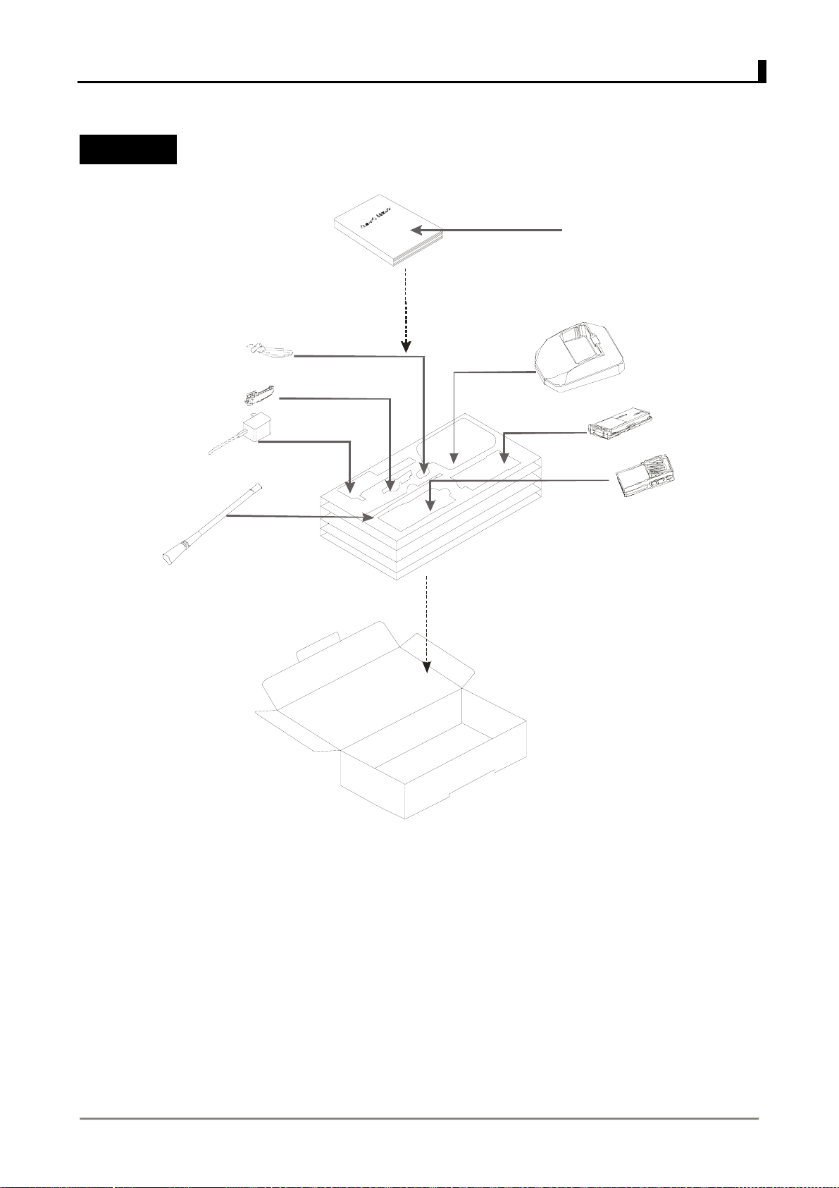
Packing
RPV516/RPU416 Packing
Owner's Manual
Belt Clip
Adapter
Antenna
Portable Strip
Gift Box
Ch arg er
Battery
Main Unit
- 34 -
Page 37
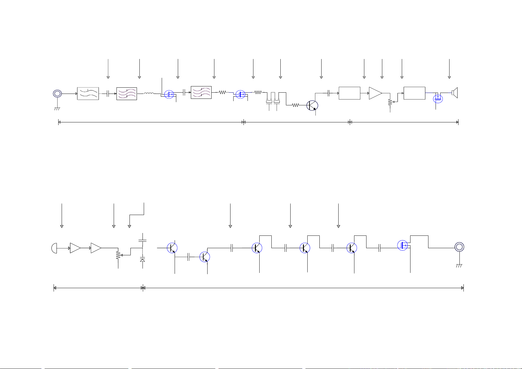
q
Rx Section
ANT
Tx Section
12mVrmS 390mVrms 120mVrms
MIC
RPV516 Level Diagram
-106.5dBm
XF200
R210
-103dBm 1018mVrms
Q201
0.44Vrms 0.8Vrms
Q101
C104
C212
Q102
175mVrms
VR
C116
23.5mVrms
AF 1kHz
0.63Vrms
Q307
SPIC302IC300IC200
4.5W
Q105 ANT
L114
-116.5dBm
C137
-113dBm
L208
L221
center
RF IF 38.85MHz
-98dBm
5R
Q203
L203,L214
-103dBm
R217
Q202
1st Local
0.1Vrms
-104dBm
R211
SSG output level for obtaining 12dB/SINAD when injected to each point Modulate the AF level with a frequency of 1KHz and deviation of 1.5KHz(Narrow),
through a 470pF coupling capacitor. 3KHz (Wide). Then take the signal from the signal generator When the AF output
Measure the 1
IC500
st
Local level on a RF VTVM. has been adjusted to 0.63Vrms with the AF vol.
0.16Vrms
C34
Q4
C100
Q100
Q6
VR501
AF VTVM
Measure the audio frequency on an AF VTVM and radio frequency on a RF VTVM at high impedance . Set the MIC input to obtain a modulation factor of 60% with the transmit
uency at center and a modulation frequency of 1KHz.
fre
D5
RF VTVM
- 34 -
- 35 -
Page 38
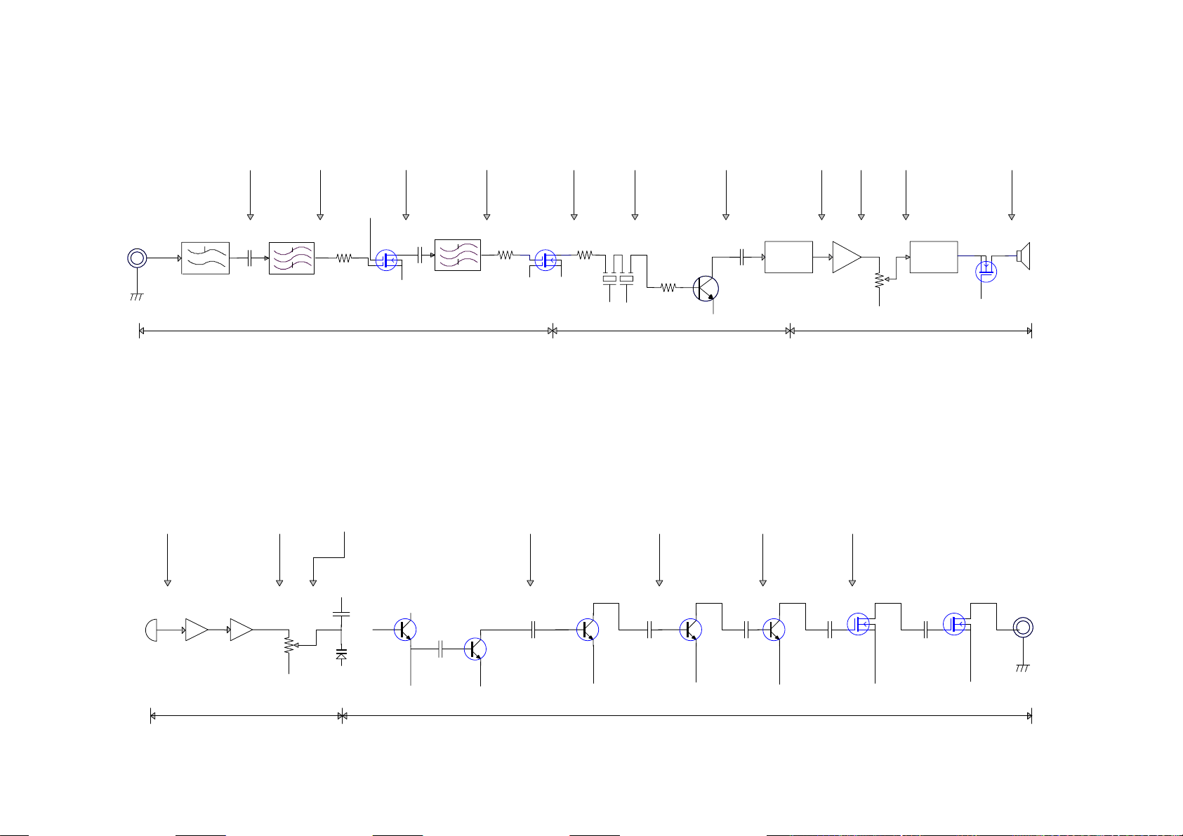
Rx Section
RPU416 Level Diagram
Tx Section
-106.5dBm
XF201
R210
-103dBm 1018mVrms
Q201
C212
175mVrms
VR
23.5mVrms
Q307
AF 1kHz
ANT
L112
-116.5dBm
C145
5R
Q203
-98dBm
-103dBm
R217
L203,L214
-113dBm
L208
R224
center
RF IF 38.85MHz
Q202
1st Local
0.1Vrms
-104dBm
R211
SSG output level for obtaining 12dB/SINAD when injected to each point Modulate the AF level with a frequency of 1KHz and deviation of 1.5KHz
through a 470pF coupling capacitor. (Narrow), 3KHz (Wide). Then take the signal from the signal generator
Measure the 1
Measure the audio frequency on an AF VTVM and radio frequency on a RF VTVM at high impedance. Set the MIC input to obtain a modulation factor of 60%
with the transmit frequency at center and a modulation frequency of 1KHz.
16mVrmS 430mVrms 310mVrms
st
Local level on a RF VTVM. when the AF output has been adjusted to 0.63Vrms with the AF vol.
0.15Vrms
0.44Vrms 0.8Vrms
0.62Vrms
Q100
- 35 -
- 34 -
C106
Q101
RF VTVM
Q102
Q105 ANT
C114
C119
Q107
MIC
IC500
C40
VR501
AF VTVM
Measure the audio frequency on an AF VTVM and radio frequency on a RF VTVM at high impedance. Set the MIC input to obtain a modulation factor of 60% with the transmit
frequency at center and a modulation frequency of 1KHz.
D5
Q4
C100
Q6
0.63Vrms
SPIC302IC300IC200
4W
- 36 -
Page 39
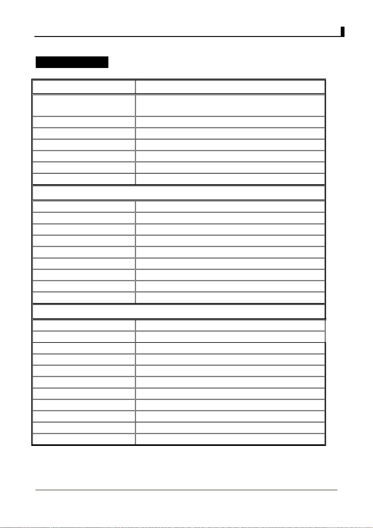
Specifications
RPV516/RPU416 Specifications
Item
Frequency range
Channel 16
Channel spacing 25KHz / 12.5KHz
Antenna impedance 50Ω
Microphone impedance 2KΩ
Operating voltage 7.5V DC
Frequency stability ±2.5×10⁻⁶
RPV516 A: 150MHz~174MHz
RPU416B: 400MHz~420MHz RPU416A: 450MHz~470MHz
Specification
Transmitter
Carrier power 4.0W
Modulation sensitivity 12±3mV
Modulation distortion ≤5%
Modulation limiting ≤5KHz / 2.5KHz
Audio response
RF Spurious emissions(Under 1 GHz) -36dBm
Adjacent channel power -70 dB / -60dB
(From 6 dB/oct. Pre-emphasis)│±3dB│
Receiver
Reference sensitivity Preceding 0.28μV or 0.35μV
Audio squelch sensitivity ≤0.4μV
Audio frequency power 500mW
Audio distortion ≤7%
Bandwidth ≥│±7 KHz│
Audio response
Co-channel rejection ≥-8 dB
Blocking ≥85dB
Adjacent channel selectivity ≥65 dB / 60dB
Spurious response rejection ≥60 d B
Intermodulation rejection ≥60 d B
(From 6 dB/oct. de-emphasis) -8dB + 2dB
The specifications may be different according to customers’ requirements
36 –
- 45 -
445
 Loading...