Software
◢ Standard Generic Attribute Profile (GATT)
◢ Android APP source code support
◢ Apple iOS APP source code support
◢ Control easily by AT commands
◢ Firmware upgrade over the UART interface
Certifications to Be Approved
◢ FCC CFR47 Part 15 (US)
Highlights
◢ Bluetooth v4.0 with Bluetooth Low Energy
(Bluetooth Smart)
◢ High-Performance and Low-Power TI CC2541
industry-standard chip
◢ Designed with PCB integrated antenna,
suitable for SMT
◢ Metal cover against EMI interference
◢ Transmitting, Receiving, Wake-up by only 2 UART pins
◢ Bluetooth Peer-to-Peer (P2P) Connection
Applications
◢ Smart phone/Tablet accessories
◢ Remote monitoring and control
◢ Indoor positioning
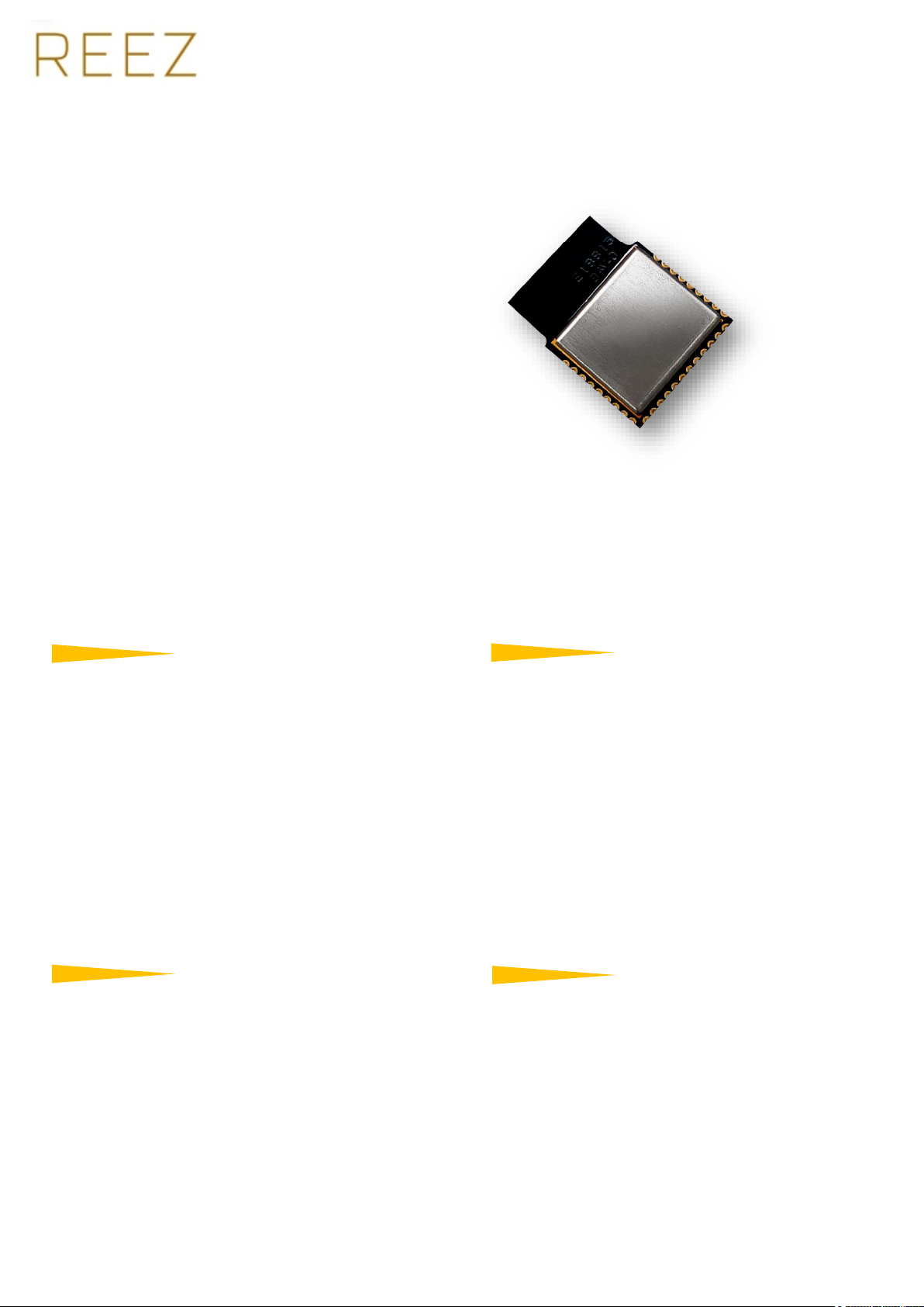
E-1100A
2.4GHz Bluetooth
Low Energy Module
with Integrated Antenna
Data Sheet
Specification
Item
Min.
Typical
Max.
Unit
Condition
Operation Voltage
2 3.6
V
VDD
RF Output Power
-23 0 0
dBm
Power Status A
8.5
mA
UART function is available
BLE is broadcasting
Power Status B
8.4
mA
UART function is available
No BLE broadcast
Power Status C
0.5
mA
UART function is sleeping
BLE is broadcasting
Power Status D
1
uA
UART function is sleeping
No BLE broadcast
Wake Up Time
30
ms
From Power Status C/D to A/B
Baud Rate
9600
57600
bps
RF Frequency Range
2379
2496
MHz
Communication Range
10 M
Open Space
Operating Temperature
-40
25
+85
˚C
Antenna
Embedded PCB Antenna
Dimensions
16.7mm*13mm*2.2mm
Weight
0.8 g
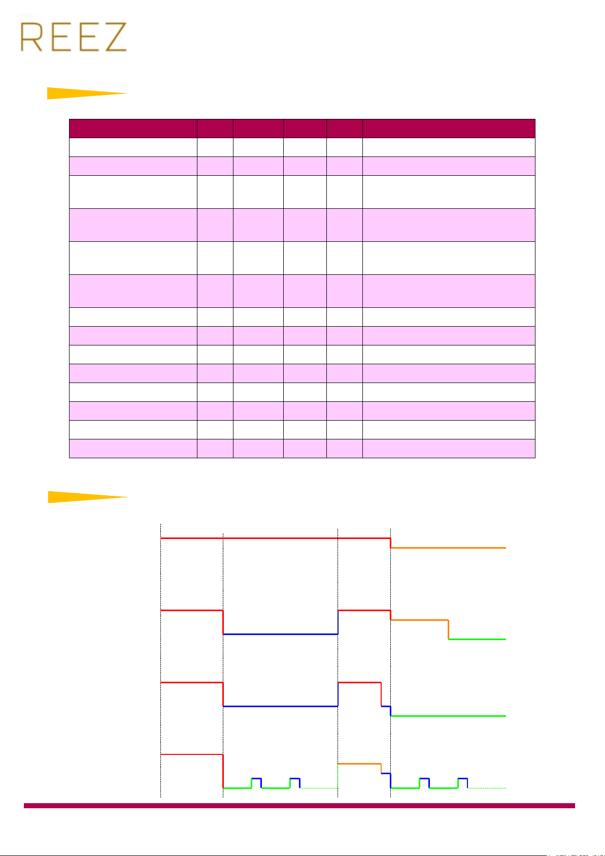
RYB070I RESET AT+PWMODE=1
Broadcast
UART FUNCTION
POWER STATUS A 8.5mA
POWER STATUS B 8.4mA
POWER STATUS C 0.5mA
UART FUNCTION
Broadcast
UART FUNCTION
UART FUNCTION
AT+PWMODE=3
AT+PWMODE=2
AT+CFUN=0
Broadcast
UART FUNCTION
AT+PWMODE=4,001,030
Broadcast
Broadcast
POWER STATUS D 1uA
Broadcast
30sec
1Sec
Broadcast
1Sec
30sec
Broadcast
circle
UART FUNCTION
AT+PWMODE=2
POWER STATUS A 8.5mA
POWER STATUS B 8.4mA
POWER STATUS C 0.5mA
POWER STATUS D 1uA
POWER STATUS A 8.5mA
POWER STATUS B 8.4mA
POWER STATUS C 0.5mA
POWER STATUS D 1uA
POWER STATUS A 8.5mA
POWER STATUS B 8.4mA
POWER STATUS C 0.5mA
POWER STATUS D 1uA
RXD TRIGGER
5sec
30sec
1Sec 1Sec
30sec
circle
5sec
1Sec
Function
Function
Function
Function
Available Power Mode and Power Consumption Status
2
Wake Up UART Functions
Ux
RYB070I
NC
5
NC
14
TXD
8
RESET_N
4
NC11NC12NC
13
VDD
29
GND
16
VDD
3
NC
6
GND
2
RXD
7
NC
10
NC
28
NC
9
GND
30
GND
15
NC17NC18NC19NC20NC
21
NC
27
NC
26
NC
25
NC
24
NC
23
NC
22
RF(External Antenna Version Used)
1
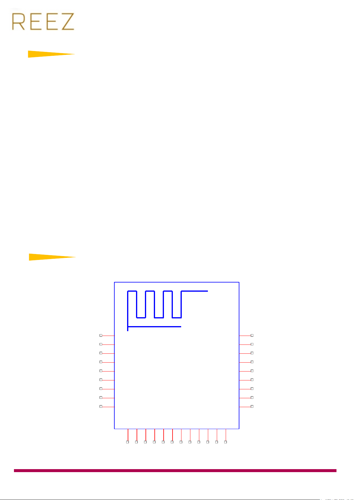
When E-1100A is on Power Status C or Power Status D, users could use pin7 RXD to wake up the UART
function. It will need some time to work normally after leaving low energy mode. In the process of
waking up the UART function, the AT command may not be recognized by E-1100A, so the data of
former bytes may be garbled. Users just need to send the commands again.
When E-1100A is on PWMODE =2 / 3 / 4, the status will be as follows after trigger by the RXD (pin7):
PWMODE =2 : E-1100A will become PWMODE =1 from PWMODE =2.
Send PWMODE =2 commands again to get back to power saving status.
PWMODE =3 : E-1100A will become Power Status A. It will return to Power Status C if there's no any
communication on UART after 5 seconds.
PWMODE =4 : E-1100A will become Power Status A, but will still do BLE broadcast and sleep on
schedule as the setting. When it is on Power Status A, it will leave PWMODE=4 after
sending PWMODE=1.
Pin Description
3

Pin
Name
I/O
Condition
1
RF External Antenna Version Used
2
GND
-
Ground
3
VDD
I
Power Supply
4
RESET_N
I
Low Reset
5
NC - Leave Unconnected.
6
NC - Leave Unconnected.
7
RXD
I
UART Data Input
8
TXD
O
UART Data Output
9
NC - Leave Unconnected.
10
NC - Leave Unconnected.
11
NC - Leave Unconnected.
12
NC - Leave Unconnected.
13
NC - Leave Unconnected.
14
NC - Leave Unconnected.
15
GND
-
Ground
16
GND
-
Ground
17
NC - Leave Unconnected.
18
NC - Leave Unconnected.
19
NC - Leave Unconnected.
20
NC - Leave Unconnected.
21
NC - Leave Unconnected.
22
NC - Leave Unconnected.
23
NC - Leave Unconnected.
24
NC - Leave Unconnected.
25
NC - Leave Unconnected.
26
NC - Leave Unconnected.
27
NC - Leave Unconnected.
28
NC - Leave Unconnected.
29
VDD
I
Power Supply
30
GND
-
Ground
4
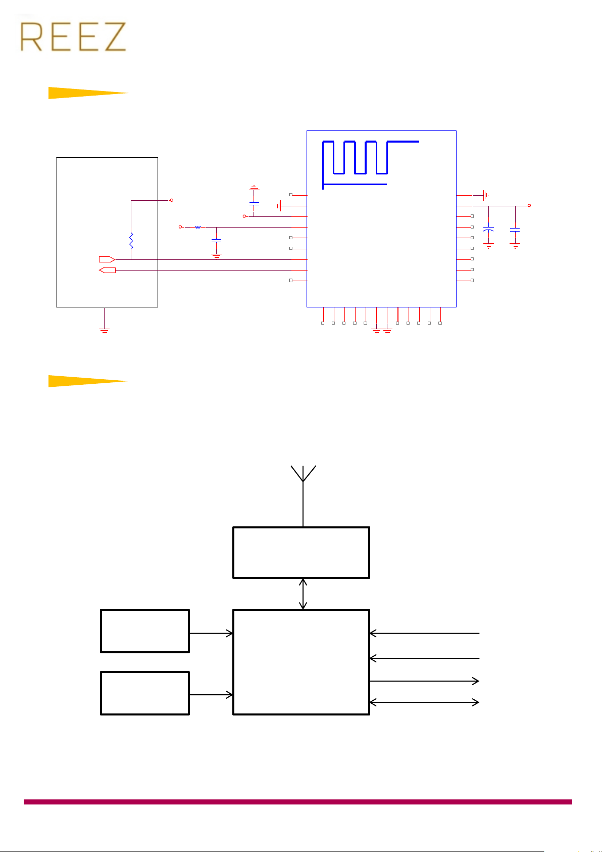
Application Circuit
RESET_N
RXD
RXD
TXD
Processor
C4
1nF
U1
RYB070I
NC
5
NC
14
TXD
8
RESET_N
4
NC11NC12NC
13
VDD
29
GND
16
VDD
3
NC
6
GND
2
RXD
7
NC
10
NC
28
NC
9
GND
30
GND15NC17NC18NC19NC20NC
21
NC
27
NC
26
NC
25
NC
24
NC
23
NC
22
RF(External Antenna Version Used)
1
+
C2
22uF
R
VDD
VDD
R1
10K
C1
0.1uF
C3
0.1uF
TXD
VDD
VDD
TI CC2541
BLE SOC
32768Hz
Crystal
32MHz
Crystal
RF Match Schematic
RESET
TXD
RXD
19 GPIO
Block Diagram
5
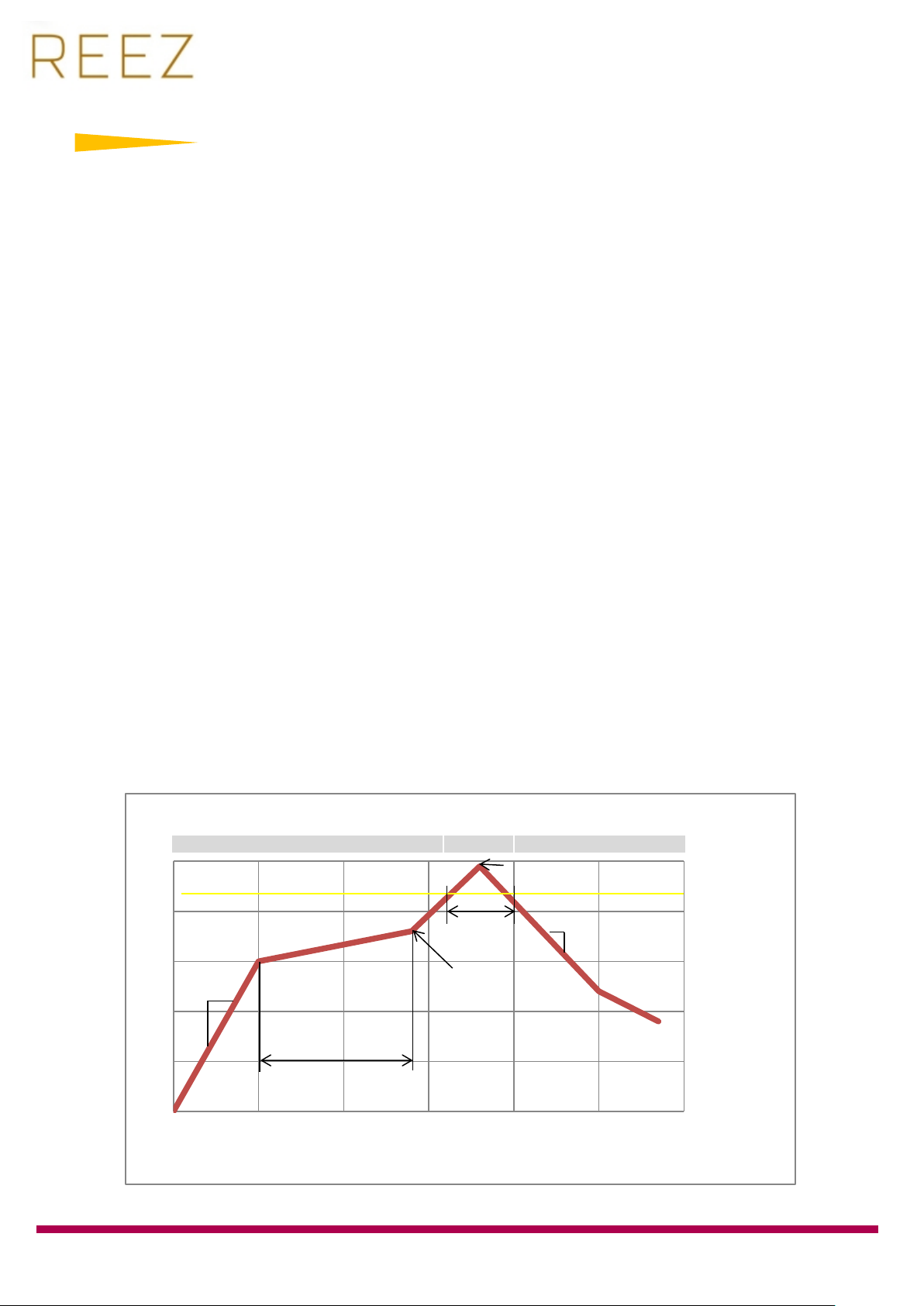
Reflow Soldering
0
50
100
150
200
250
0 50 100 150 200 250 300
座標軸標題
Y 值
Y 值
[°C]
217
Max 3°C/s
Liquidus temperature
60-120s
End Temp
150-200°C
40-60s
Max 4°C/s
Typical Leadfree
Soldering Profile
Preheat
Heating
Cooling
Elapsed Time
Recommended soldering profile
Peak Temp245°C
Consider the "IPC-7530 Guidelines for temperature profiling for mass soldering (reflow and wave)
processes, published 2001.
Preheat phase
Initial heating of component leads and balls. Residual humidity will be dried out. Please note that
this preheat phase will not replace prior baking procedures.
◢ Temperature rise rate: max. 3 °C/s If the temperature rise is too rapid in the preheat phase it may
cause excessive slumping.
◢ Time: 60 - 120 s If the preheat is insufficient, rather large solder balls tend to be generated.
Conversely, if performed excessively, fine balls and large balls will be generated in clusters.
◢ End Temperature: 150 - 200 °C If the temperature is too low, non-melting tends to be caused in
areas containing large heat capacity.
Heating/ Reflow phase
The temperature rises above the liquidus temperature of 217°C. Avoid a sudden rise in temperature
as the slump of the paste could become worse.
◢ Limit time above 217 °C liquidus temperature: 40 - 60 s
◢ Peak reflow temperature: 245 °C
Cooling phase
A controlled cooling avoids negative metallurgical effects (solder becomes more brittle) of the
solder and possible mechanical tensions in the products. Controlled cooling helps to achieve bright
solder fillets with a good shape and low contact angle.
◢ Temperature fall rate: max 4 °C/s To avoid falling off, the REEZ E-1100A module should be placed
on the topside of the motherboard during soldering.
6

Dimensions
5.6±0.1
11.6±0.2
0.7±0.1
0.8±0.1
1.4±0.1
13.0±0.3
0.6±0.1
1.1±0.1
5.2±0.1
13.0±0.3
16.7±0.3
10.4±0.2
0.7±0.1
0.8±0.1
1.4±0.1
16.7±0.3
Unit : mm
7

Layout Footprint Recommendations
Top layer
Anti copper area
Bottom layer
Copper area
1.0±0.1
16.7±0.3
0.8±0.1
0.5±0.1
1.0±0.1
13.0±0.3
1.0±0.1
0.7±0.1
Anti cooper area
Unit : mm
8

AT Command
Syntax
Response
AT
+OK
Syntax
Response
AT+RESET
+RESET!
Syntax
Response
AT+NAME=<name>
<name> at most 20 ASCII characters
Example: set the broadcast name
as“REYAX_BLE_RYB070I”
AT+NAME= REYAX_BLE_RYB070I
* It will work after sending
AT+RESET
or
pressing RESET bottom.
+OK
AT+NAME?
+NAME= REYAX_BLE_RYB070I
Syntax
Response
AT+ATTR=<attribute>
<attribute> at most 20 ASCII characters
Example: set the device name
as“REYAX_BLE_RYB070I”
AT+ATTR= REYAX_BLE_RYB070I
* It will work after sending
AT+RESET
or
pressing RESET bottom.
* Some iOS APP use this name to recognize
the Bluetooth device.
+OK
AT+ATTR?
+ATTR= REYAX_BLE_RYB070I
It is required to key in “enter” or “\r\n” in the end of all AT Commands.
Add“ ? ”in the end of the commands to ask the current setting value.
1. AT to test if the module responds
2. Software RESET
3. AT+NAME to set the broadcast name
4. AT+ATTR to set the device name
9

5. AT+CRFOP to set the RF output power
Syntax
Response
AT+CRFOP=<power>
<power> range 1 to 3
1:0dBm (default)
2:-6dBm
3:-23dBm
Example: set the output power as -6dBm
AT+CRFOP=2
+OK
AT+CRFOP?
+CRFOP=2
Syntax
Response
AT+CFUN=<Advertising>
<Advertising> is the switch of BLE broadcast
0:BLE broadcast off
1:BLE broadcast on (default)
Example: set the BLE broadcast off
AT+CFUN=0
+OK
AT+CFUN?
+CFUN=0
Syntax
Response
AT+CNE=<Connect>
<Connect> set the BLE can be connected or
not
0:Reject other Bluetooth devices connecting.
1:Accept other Bluetooth devices connecting
(default)
Example:Reject other Bluetooth devices
connecting
AT+CNE=0
+RESET!
AT+CNE=0
+RESET!
6. AT+CFUN to set the BLE broadcast (Advertising) ON/OFF
7. AT+CNE to set the BLE can be connected or not
10

8. AT+PWMODE to set the power mode
Syntax
Response
AT+PWMODE=<mode>
<mode> is the power saving mode
1:Power Saving Mode 1 (default)
2:Power Saving Mode 2
3:Power Saving Mode 3
4:Power Saving Mode 4 (Only in Peripheral mode)
Example: use Power Saving Mode 3
AT+PWMODE=3
+OK
AT+PWMODE?
+ PWMODE=3
Users could set the cycle time to switch the BLE broadcast ON/OFF in Power Saving Mode 4.
AT+PWMODE=4<,time of BLE broadcast ON>,<time of BLE broadcast OFF>
(Unit of time: Second)
The second must be three-digit number.
The minimum is 1 second, the maximum is 600 seconds. (001~600)
Example: Setting the BLE broadcast cycle time as ON for 3 seconds and OFF for 5 seconds.
AT+PWMODE=4,003,005
If users don't set the parameter of time, the default is:
ON for 5 seconds and OFF for 10 seconds.
Syntax
Response
AT+CONNECT?
+CONNECT=0 (unconnected)
+CONNECT=1 (connecting)
9. AT+CONNECT? to inquire the connection status
11

10. AT+IPR to set the UART baud rate
Syntax
Response
AT+IPR=<rate>
<rate> is the UART baud rate
4:9600 (default)
5:19200
6:38400
7:57600
Example: set the baud rate as 57600, it will
memorize the setting and reset the module.
AT+IPR=7
+OK
AT+IPR?
+IPR=7
Syntax
Response
AT+ADDR?
+ADDR=123456ABCDEF
Syntax
Response
AT+ENTER=<state>
<state> is whether needed to key in ENTER
(0x0D
0x0A)
in the end of the commands.
0:no need
1:needed (default)
Example: setting there’s no need to key in
ENTER
(0x0D 0x0A)
in the end of the commands,
it will memorize the setting and reset the
module.
AT+ENTER=0
+OK
AT+ENTER?
+ENTER=0
11. AT+ADDR to inquire MAC address
12. AT+ENTER to set if needed to key in ENTER
(0x0D 0x0A)
in the end of the commands
12

13. AT+AUE to set if the module follows the Connection Parameter Update Request automatically
Syntax
Response
AT+AUE =<0/1>
<0/1> is the switch of this function
0 : Not to follow automatically (default)
1 : Following automatically
Example: Setting the module not to follow
the Connection Parameter Update
Request automatically, it will memorize the
setting and reset the module.
AT+AUE=0
* Setting the module follow the Connection
Parameter Update Request may cause the
BLE connection unstable in iOS.
+OK
AT+AUE?
+AUE=0
Syntax
Response
AT+CGMS?
+CGMS=RYB070I_56312E34
Syntax
Response
AT+ROLE=<role>
<role> is Peripheral or Central
0:Peripheral (default)
1:Central
Example: set the role as Central, it will
memorize the setting and reset the module.
AT+ROLE=1
+OK
AT+ROLE?
+ROLE=1
14. AT+CGMS? to inquire the firmware version
15. AT+ROLE to set the role as Peripheral or Central
13

16. AT+SCAN to scan the Peripherals near by the Central
Syntax
Response
AT+SCAN
+<MAC>,<rssi>
+Found <Quantity>
+<NO.>:<MAC>
<MAC> MAC address
<rssi> output power of Peripherals: -xxdBm
<Quantity> quantity of found Peripherals;
the maximum is 8.
<NO.> item number of Peripherals: 1~8
+123456ABCDEF,-79dBm
+1237F3AB54CA,-60dBm
+Found 2
+1:123456ABCDEF
+2:1237F3AB54CA
Syntax
Response
AT+CON=<MAC>
<MAC> MAC address
Example: the Central connect to the Peripheral
whose MAC address is 123456ABCDEF
AT+CON=123456ABCDEF
+Connected
17. AT+CON The Central connect to a Peripheral by MAC address
14

18. AT+CONT The Central connect to a Peripheral by the item number from AT+SCAN
Syntax
Response
AT+CONT=<NO.>
<NO.> the item number of the Peripherals: 1~8
Example: the Central connect to the Peripheral
whose item number is 2 from AT+SCAN
AT+CONT=2
+Connected
Syntax
Response
AT+DISCON
+Disconnected
Syntax
Response
After RESET
+READY
+ENTER=1
+ROLE=0
The data has been transmitted
+>>>>>
BLE is connecting
++++++
BLE is unconnected
+-----
19. AT+DISCON to disconnect the Peripheral from the Central
20. Other response messages
* Our Company is not responsible for any technical malfunction or other problems if users modify the
module by themselves.
15

Transmission Data Size
[1] The maximum transmission data size from E-1100A to smartphones APP is as follows:
When AT+ENTER=1 (default), it is needed to add
the maximum data size is 18 bytes each time.
When setting AT+ENTER=0, it is no need to add
the maximum data size is 20 bytes each time.
[2] The maximum transmission data size from smartphone APP to E-1100A is 20 bytes each time.
0x0D 0x0A
0x0D 0x0A
(2 bytes) in the end of each data, so
(2 bytes) in the end of each data, so
16

Certifications
2AMMC-E-1100A
FCC Statement:
This device complies with part 15 of the FCC Rules. Operation is subject to the following two conditions:
(1) This device may not cause harmful interference, and
(2) this device must accept any interference received, including interference that may cause undesired operation.
NOTE: This equipment has been tested and found to comply with the limits for a Class B digital device, pursuant to part 15 of the FCC
Rules. These limits are designed to provide reasonable protection against harmful interference in a residential installation.
This equipment generates, uses and can radiate radio frequency energy and, if not installed and used in accordance with the
instructions, may cause harmful interference to radio communications. However, there is no guarantee that interference will not
occur in a particular installation.
If this equipment does cause harmful interference to radio or television reception, which can be determined by turning the
equipment off and on, the user is encouraged to try to correct the interference by one or more of the following measures:
—Reorient or relocate the receiving antenna.
—Increase the separation between the equipment and receiver.
—Connect the equipment into an outlet on a circuit different from that to which the receiver is connected.
—Consult the dealer or an experienced radio/TV technician for help.
Changes or modifications not expressly approved by the party responsible for compliance could void the user’s authority to operate
the equipment.
LABEL OF THE END PRODUCT:
The final end product must be labeled in a visible area with the following " Contains TX FCC ID : 2AMMC-E-1100A ". If the size of the
end product is larger than 8x10cm, then the following FCC part 15.19 statement has to also be available on the label: This device
complies with Part 15 of FCC rules. Operation is subject to the following two conditions: (1) this device may not cause harmful
interference
and (2) this device must accept any interference received, including interference that may cause undesired operation.
17
 Loading...