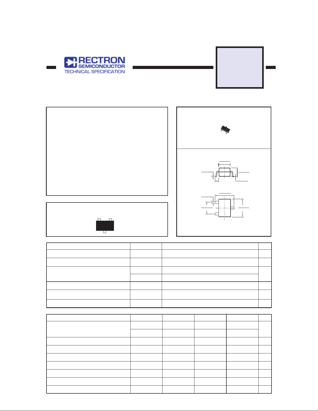
SOT-323 DIGITAL TRANSISTORS
TRANSISTORS(PNP)
FEATURES
Built-in bias resistors enable the configuration of an inverter
*
circuit without connecting external input resistors.(see equivalent circuit).
The bias resistors consist of thin-film resistors with co-
*
mplete isolation to allow negative biasing of the input.
They also have the advantage of almost completely Eliminating parasitic effects.
Only the on/off conditions need to be set for operation mark-
*
ing device design easy.
MECHANICAL DATA
* Case: Molded plastic
* Epoxy: UL 94V-O rate flame retardant
* Lead: MIL-STD-202E method 208C guaranteed
* Mounting position: Any
* Weight: 0.006 gram
MAXIMUM RATINGS AND ELECTRICAL CHARACTERISTICS
Ratings at 25OC ambient temperature unless otherwise specified.
MAXIMUM RATINGES ( @ TA = 25oC unless otherwise noted )
Supply voltage
Input voltage
Output current
Power dissipation
Junction temperature
Storage temperature
ELECTRICAL CHARACTERISTICS ( @ TA = 25oC unless otherwise noted )
CHARACTERISTICS SYMBOL UNITS
Input voltage (VCC= -5V, IO= -100mA)
Input voltage (VO= -0.3V, IO= -2mA)
Output voltage (IO /
= -10mA / -0.5mA)
II
Input current (VI= -5V)
Output current (VCC= -50V,VI= 0)
DC current gain (VO= -5V,IO= -5mA)
Input resistance
Resistance ratio
Transistion frequency (VO= -10V,IO= 5mA, f= 100MHz)
NOTE: "Fully ROHS compliant", "100% Sn plating (Pb-free)".
RATINGS
(2)
(1)
(1) IN
(2) GND
(3)
(3) OUT
SYMBOL
V
CC
V
IN
I
O
IC(MAX)
Pd
Tj
Tstg
V
I(off)
V
I(on)
V
o(on)
I
I
I
o(off)
G
I
R
1
R2 / R
1
f
T
DTA144EUA
0.053(1.35)
0.045(1.15)
0.006(0.15)
0.003(0.08)
REF 0.021(0.53)
0.096(2.45)
0.016(0.40)
0.008(0.20)
0.055(1.40)
0.047(1.20)
0.085(2.15)
1
2
Dimensions in inches and (millimeters)
LIMITS
-50
-40~+10
-30
-100
200
150
-55 ~150
MIN
-
-3
-
TYP
-
-
-
- - -0.18
-
68
32.9
0.8 1.2
-
-
47 61.1
1
- 250 -
0.004(0.10)
0.000(0.00)
3
0.043(1.10)
0.035(0.90)
0.087(2.20)
0.079(2.00)
MAX
-0.5
-0.3
-0.5
-
-
SOT-323
UNITS
MHz
V
V
mA
mW
o
C
o
C
V
V
mA
mA
-
KW
-
2006-3

RATING AND CHARACTERISTICS CURVES (DTA144EUA)
-100
-50
-20
-10
-5
-2
INPUT VOLTAGE, (V)
-1
I(on),
V
-500m
-200m
-100m
-100m -200m -500m
1K
500
200
100
50
20
10
, DC CURRENT GAIN
i
G
5
2
1
-100m -200m -500m
VO= -0.3V
Ta=-40OC
25OC
100OC
-1m -2m -5m -10m -20m -50m -100m
I
OUTPUT CURRENT, (A) V
Ta= 100OC
25OC
-40OC
O,
VO= -5V
Figure1 Input voltage vs. output current
(ON Characteristics)
-1m -2m -5m -10m -20m -50m -100m
I
OUTPUT CURRENT, (A) IO, OUTPUT CURRENT, (A)
Figure3 DC current gain vs. output current
O,
-10m
VCC= -5V
-5m
-2m
Ta= 100OC
-1m
-500m
-200m
-100m
-50m
-20m
OUTPUT CURRENT, (A)
O,
I
-10m
-5m
-2m
-1m
0
-1
-500m
-200m
-100m
-50m
-20m
-10m
CUTPUT VOLTAGE, (V)
-5m
O(on),
V
-2m
-1m
-100m -200m -500m
25OC
-40OC
-0.5 -1.0 -1.5 -2.0 -2.5 -3.0
INPUT VOLTAGE, (V)
Figure2 Output current vs input voltage
I(off),
(OFF Characteristics)
Ta= 100OC
25OC
-40OC
-1m -2m -5m -10m -20m -50m -100m
Figure4 Output voltage vs. output current
IO / II= 20
R
1
IN
R
2
IN
GND(+)
OUT
GND(+)
OUT
Figure5 Equivalent circuit
 Loading...