


ADL}OO/ADAI2OO
Userts Manual
Real
IISSOO99000011 aanndd AASS99110000 CCeerrttiiffiieedd
Time
"Accessing
Devices,
the Analog
Inc.
World',,

ADLaOO/ADA12OO
Userts
Manual
ffi
REAL
State
TIME
820 North
Post
College, Pennsylvania
Phone: (8141234A087
FAX:
University Drive
Office Box
(81a)
DEVICES,
234-5218
INC.
906
16804
USA

Published
Real
Time Devices,Inc.
820 N.
University Dr.
P.O.
Box
State College,
by
906
PA 16804
USA
Copyright @ 1992
by Real Time
All rights
Printed
in
Devices,Inc.
reserved
U.S.A.
Rev.A 9234

Table
of
Contents
INTRODUCTION
Digital-to-Analog
What Comes
Applications
CHAPTER 1
Factory-Configured
P3 - Analog
-
P4
Analog
-
P5
DMA
P6 - DMA
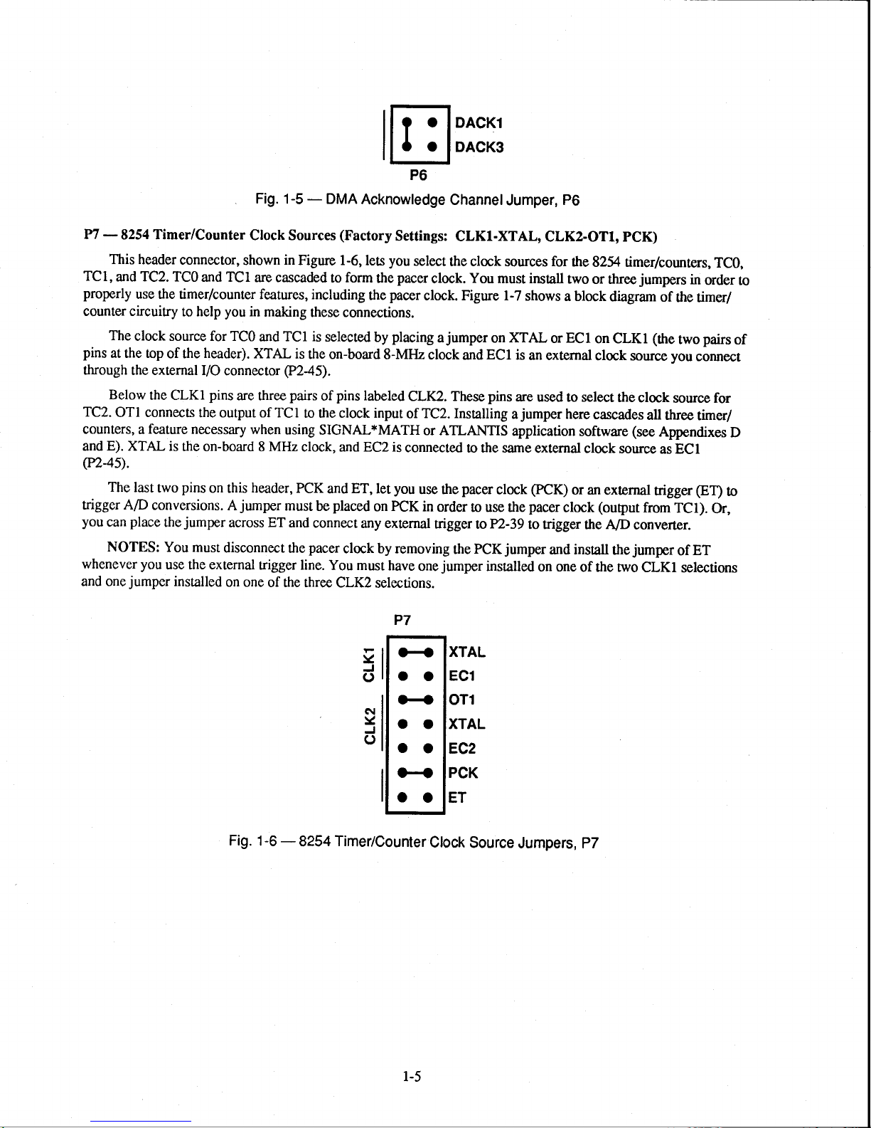
-8254
P7
-
P8
Intemrpt
-
P9
DAC
-
P10
Pl I
Plz
Sl - Base
Pull-up/Pull-down
-
-
DAC
A/D
A/D
Conversion
With Your
Software
-
BOARD
Input
Input
Request
Acknowledge
Timer/Counrer
Source
I
Output Voltage Range
2
Output Volrage
Data
Converter
Address
Resistors
(ADA1200
Toolkit
and
SBTTINGS
Switch and Jumper
Voltage Range
Voltage Polarity
Channel
Channel
Clock Sources
and Channel
Word Bit
State Set
Status,/External
(Facory
on
(Facrory
(Factory
(Factory
Range
Setting:
Digital
I/O
(Factory
(Facory
(Facory
Only)...........
Settings
Setring: t0
(Facory
(Factory
Gate
300 hex
Seuing:
Setting:
Lines.....
Disabled).....
Sening: Disabled)
@acory
Setting:
Seuing:
Sening: +5
Setting: +/-)
2 Monitor
(268
Volrs)......
+/-)
..............
Serings:
Jumpers
-5
+5
to
o
.............
@actory
decimal)
CLKI-XTAL,
on OT2
volts)
-5
volts)............
Setting: EOC
.................
& G;
..........
CLK2-OT1,
Inremrpt
(A/D
Chs
Converter
..........................t-3
............i4
...............1-3
.......................
.....................14
pCK)
...................1-5
Disabled)
.....................
Status))
..............1_9
14
........... 14
......14
......... l-6
.........1_7
......1_g
l_g
....... l-9
.......1_10
i-l
CHAPTER 2
Connecting
Connecting
Connecting
Connecting
Running
CHAPTER
D/A
Converte
Di$tal I/O, Programmable
_
BOARD
Analog
the
Trigger
the
the Analog
Timer/Counters
the
the 1200DIAG
-
3
HARDWARE
INSTALLATION
Input Pins
In
Trigger
and
Outpurs
Diagnostics
Peripheral Interface
Out
(ADAI200
and Digital
Prrogram
DESCRIPTION
pins,
Cascading
Only)...........
...............
VO
...........
8oards.........
2-l
............24
..............24
..................2-s
..................2_5
...................2_s
.............3-1
.................3_5

CHAPTER 4 - BOARD
OPERATION AND
PROGRAMMING
BA +
0: Read
BA + l:
BA + 2:
BA + 4:
BA +
5: PPI
BA +
6: PPI Port
BA +
7:
BA +
8:
BA +
9:
BA+
l0:
BA+
11:
BA + 12:
BA
+ 13:
BA +
14:
BA +
15:
Clearing
Initializing
Enabling
Enabling
Conversion Modes/Triggering
Starting
Monitoring
Reading
Programming
Sntus/Srart
Read A/D Data/Update DAC
(Write
Reset
PPI Port A - Digital
Port
B
C
PPI
8255
SZl4TimerlCounrer0
8254 Timer/Countor I
8254Timer/Counr€r2(ReadAMrite)
S254ConrolWord(WriteOnly)...........
D/A
D/A
D/A
D/A
and Setting Bits
an A/D
the
Conrol Word
Converter 1 LSB: ADA1200
Converter 1 MSB: ADAI200
Converter
Converter
Disabling
and
Disabling
and
Conversion
Conversion
Converted Data
the Pacer
Convert
Only) ..........
-
Channel8oard
-
Digital
2 LSB: ADAI200
2 MSB: ADA12200
in
the
Intemrprs
Status
Clock
(Readl'\Mrire)
Outputs
(ReadAMrire)
VO
Functions
(Readflilrire)
VO
(Write
Only) ...........
(ReadAMrite)
(Read/lMri9
Extemal
............
Trigger
............
Done
@MA
..................
(Read/Write)
................
(Readflilrite)
Select
................
(Wrire
Only) ..........
(Wrire
Only) ...........
(Wrire
Only)
..........
(Write
Only) ...........
.....
or End-of-Convert)
.........44
...........44
...........44
...............4-5
..................4-5
................4-5
.......................4-5
...............4-7
...............4-7
.............4-7
.......4-7
......4-g
.........................4-g
......4-g
.......................4-g
....................4-12
......4-12
.....................4-12
..........,.....4-13
......................4-13
...4-13
...............4-14
8259 Programmable
Intemrpt
End-of-Interrupt
What
Using
Writing
Saving
Restoring
Common
Choosing
Allocating
Calculating
Setting
The
DMA
Programming
Programming
Mask Register
Exactly
Intemrpts in Your
Interrupt
an
the startup
the
Interrupt Mistakes
DMA
a
DMA Buffer
a
the
the DMA Page Register...................
DMA
Mask
Single
Intemrpt
(IMR)
(EOI)
Command
llappens When
Programs..........
Service
Intemrpt
Startup
Channel
Page
Register
DMA
the
the 1200 for DMA.....
Mask Register (IMR)
IMR
and Interrupt
and Offset
Controller
Controller
..........
Intemrpt
an
Routine (ISR)
of a Buffer
Occurs?
Vector
and
Intemrpt
vector
.................4-16
......................4-16
......4-16
.....................4-16
................4-16
.............4-17
..........4-tg
.....4-lg
...............4-19
..................4-19
...................4-19
............4-20
............4-2t
................4-Zz
.....4-23
.,4-23

Monitoring for DMA Done............
Common
D/A
Conversions
DMA Problems
(ADA1200
...............
Only)
.....4-23
....4-24
........4-2,4
Example Programs
Single Convert
DMA Flow Diagram
Interrupts Flow Diagram
D/A
Conversion
Flow Diagrams
and
Flow Diagram
(Figure
(Figure
Flow Diagram
4-5)..............
CHAPTER 5 _ CALIBRATION
APPENDIX A - 12OO
APPENDIX B - P2
APPENDIX
APPENDIX D
APPENDIX E
APPENDIX F
C - COMPONENT
_
_
-
SPECIFICATIONS
CONNECTOR PIN ASSIGNMENTS
CONFIGURING THE
CONFIGURING
WARRANTY
(Figure
44)
4-6)
.............
(Figure
4-7).
......
DATA
SHEETS
12OO FOR
THE 12OO
.............
....
SIGNAL
MATH
FOR ATLANTIS.........
......4-27
.....................4-29
..............4-30
........4-3I
..........4-32
A-l
.........8-1
D-1
.......E.T.
F-1
ul

iv

LIST
ILLUSTRATIONS
OF
l-l
t-2
t-3
T4
1-5
r-6
r-7
t-8
r-9
l-10
l-l I
t-12
l-13
l-t4
l-15
1-16
t-17
l-18
2-r
2-2
2-3
3-1
3-2
4-I
4-2
4-3
4-4
4-5
4-6
+-t
5-1
Board Layout
Analog Input
Analog Input
DMA Request
DMA
Acknowledge
&254Timer/Counter
8254 Timer/Counter
Intemrpt
Pulling Down
DAC
I
DAC 2
A/D Data
A/D
Converter
Base Address
Pull-up/Pull-down
Adding Pull-ups
Gain Circuiny
Diagram
n
Connector Pin Assignmens
UO
Analog Input
Cascading
ADI200/ADA1200
S2l4TimerlCounter
A/D
Conversion Timing
Pacer
Clock
8254Timer/Counter
Single Conversion Flow Diagram
DMA Flow Diagram
Interrupts Flow
D/A
Conversion Flow
Showing Factory-Configured
Voltage Range
Voltage Polarity
Channel Jumper, P5
Channel Jumper, P6................
Clock Source
Circuit Block Diagram
Channel Jumper,
Intemrpt Request
the
Voltage
Output
Output Voltage Range
Word Bit
for Removal
Two
Block
State Set Jumper, Pll
StatuslExternal
Switch, Sl ................
Resistor
Pull-downs
and
Formulas
and
Connections
Boards for
Block
Circuit
Diagram
Circuit Block Diagram
Diagram
Jumper, P3
Jumper, P4
P8
...............
Range
Jumper,
Jumper, P10
Gate
Circuitry....
for
Calculating
of Solder Short
............
Simultaneous
Diagram
Block
Diagram, All
.................
Diagram
(ADA1200
to
Settings...................
...............
................
Jumpers, P7................
.....................
Line
............
P9
................
..............
2 Monitor
Digital
...........
.............
Diagram
Modes....
Jumper, P12..............
Lines
VO
Gain
and f ............
Sampling
Only)...........
..................
...................14
................14
.....................14
..................1-5
................1-6
......................1-z
................1-8
................1-8
........... l-9
...........1-9
......................1-9
.............. l-l
.............1-12
..................1-13
........................24
.................2-6
.....................3-3
.....................4-12
...........4-15
.......................4-Zg
....................4-31
1-3
........1-5
........1-6
I
..... 1-14
.........2-3
........34
......4-25
.......4-32


INTRODUCTION


The ADl200
high-speed, high-performance
a
computer, each
.
16
single-ended analog input
.
l2-bit,5 microsecond
.
15, tl0,
.
Resistor
.
Three
.
.
.
'
.
.
.
The following
functions
board
conversion
DMA
transfer,
Trigger
16 TTL/CMOS
Three l6-bit
Two 12-bit
+5, +10,
Turtro Pascal,
setup
in
is included in
is
described in
ADA1200
and
1200
series
board features:
analog+o-digital
+10 volt
or 0 to
configurable
and trigger out for
timer/counters
digital-to-analog
+5,
0 to
Turbo
paragraphs
gain,
modes,
8255-based
or 0 to
C, and BASIC
Chapter
Chapter
Advanced
data
acquisition
channels,
input
range,
external
digital
(two
cascaded
output
+10
volt
analog output range
briefly
describe
3, Hardware
l, Board
Indusrial
converter
triggering or cascading
I/O
lines which
channels
source code; diagnostics
Operation,and
Settings.
Contol
and control
pacer
for
with
major
the
boards turn
system.
with 125 kl{z
can
be configured with
clock),
dedicated
(ADA1200
functions
Chapter 4 , Board
your
IBM
PC/XT/AT
Installed
boards,
grounds (ADA1200
program.
of the
within a
throughput,
pull-up
only),
A more
board.
Operation
single
pull-down
or
only),
detailed
and
or compatible into
expansion
Programming.Tlte
slot in
resisrors,
discussion
the
of board
Analog-to-Di
The
analog-to-digital
into
l2-bit
The
analog
unipolar range
provided
can
customize the
A,/D
are controlled
through
microprocessor
channel
memory.
through the
the
The
converted data
is
gital
digital data words which
input voltage
+ l0 volts.
of 0 to
inputs.
at the
input
conversions are
through software,
I/O
connector.
or by using
DMA
jumper
transfer
chosen by
In
the
processor.
Digital-to-Analog
The
digiral-to-analog
with individually
programmed
Data is
write
single
jumper-selectable
into
operation. Access
Conversion
(AlD)
circuitry
range
The
The high-perforrnance
gain.
performed
by an
can be Eansferred
direct memory
settings
mode,
Conversion
(D/A)
circuitry
D/A
the
converter
ttrrough
receives
can tien be
jumper-selectable
is
is
board
in
on
you
factory
A,/D
5 microseconds,
on-board
through
access
the board. The
make
can
(ADA1200
on the ADA1200
ranges
oulput
and a conversion
DMA is not
up to 16
read
converter
pacer
ttre
@MA).
continuous
single-ended
and/or transferred
for
bipolar
-5
set for
supports
and the maximum
clock,
or by an external
PC
data bus to PC memory in
The mode
PC
data bus is
Onty)
features
-5
of
+5
to
available.
volts,
is
analog
pc
to
ranges
of
+5 volts.
to
transfers
-10
automatically
Overvoltage
resistor
throughput rate
of transfer is
used to
directly o
independent
two
+10 volts,
to
inputs
and
converts
memory.
-5
+5 volts
to
configurable
trigger brought
software-selectable
read
and/or
PC
0 to +5 volts,
triggered for
or
protection
gain
is
125 kllz.
one
of two ways:
transfer
memory
l2-bit
analog
a
channel
onto the
-10
to
to
circuiry
data
wittrout
output
or 0
inpus
these
+10
volts,
or a
+35
volts
is
so that
Conversions
board
by using
and the DMA
pC
o
going
channels
+10 volts.
to
through
a
you
the
8254 Timer/Counter
An
timing and
clock. The
programmable
8254
counting
third is
functions.
available
interval
Two
for
counting
of the timerrcounters
timer
contains
applications,
three l6-bit,
are cascaded
or it can
i-3
8-MHz
be cascaded
timer/counters
and
can be used internally
to
the other
to
support
two
a wide range
for
timer/counters.
the
of
pacer

Digital
or
the on-board
resistors
VO
The
1200 has 16 TTL/CMOS-compatible
signals
to sense switch closures, trigger digital
included
are
programmable peripheral
8255
on the board.
digital I/O lines which
interface
Installation
events, or
procedures
activate
chip. Pads for installing
given
are
can be directly interfaced
solid-state
near
relays.
and activating
end
the
ofChapter l,Board
These lines
with external
provided
are
pull-up
pull-down
or
Settings.
devices
by
What
(814)
Board
hardware
for help
Application
SIGNAL*MATH
ATLANTIS
high level
NOTEBOOK/XE,
Programmer's
Hardware
Comes With
You
receive
.
ADl200
.
Software
.
User's
If
any item is missing
234-8087. If
the following items in
or
and diagnostics diskette
manual
Accessories
In
addition
in
Our
to
accessories.
choosing the
Software
custom application software
for real-time monitoring and
interfaces
Toolkit
Accessories
Your Board
ADAI200 interface
or damaged,
you
require
the items included in
Call
and Drivers
for integrated
between the 1200
LTICONTROL. rtdlinx
and
provides
service outside
your
items to
best
local
distributor
support
packages
dara acquisition
routines with
your
board
with
please
your
data
and
package:
1200
Turbo Pascal, Turbo
call Real Time Devices'
the U.S., contact
package,
1200
or our
your
board's application.
provide
and sophisticated
acquisition. rtdlinx
custom or third
source
documented source
and BASIC
C,
Customer
your
local disnibutor.
Real Time Devices
main
office for more information
excellent data acquisition
digital signal
rtdlinx/ablinx
and
party
software,
code
is
available
code
for
for
offers a
including
a one-time fee.
cuslom
source
code
Service Department
full line
about these
and analysis
processing
drivers
LABTECH
progrcmming.
of software
support.
and analysis,
provide
NOTEBOOK,
Our Pascal
at
and
accessories and
Use
or
full-featured
and C
Hardware
input
channel
boards,
prototype/terminal
XB50
boards
for simplified
assembly for
OP
series
accessories
your
on
extemal
1200
optoisolated digiual
testing and debugging
interfacing.
Using This Manual
This
manual is intended
enough
complex
can customize
When You
information
contact,
eastern
include
problem.
detail about the board and
applications.
the example software or
Need
This
manual and the example
properly
to
Technical
our
daylight time, or send a
your
company's
We
Help
Support
for
1200 include
the
16
to
differential
input
boards,
for
board
assume that
use all of the board's features.
name and address,
easy signal
you
help
to
Department,
FAX requesting
install your
its functions
you
write your
programs
already have
(814)
your
MX32
the
or
32 single-ended
the
access and
prototype
of
new
so
that
own
in
the software
234-8087,
assistance to
name,
analog input
input
channels,
T516
temperature sensor
prototype
circuitry, and
board and
you
can
an understanding
applications
package
you
If
during
your
telephone
development,
get
enjoy
programs.
have
any
regular
(814)
234-52L8.
maximum
included
problems
expansion
MR
board,
XP50
twisted
it
running
use of
of data
acquisition
with
installing
business hours,
When
number,
and
which
board
series
the
EX-XT
ttre
pair
quickly,
its
your
sending a
a brief description
can
mechanical
TB50
terminal
and EX-AT
wire flat ribbon
while
also
features
board
or
even
principles
provide
using ttris board,
eastern
FAX
expand a single
relay
output
board and
extender
cable
providing
in
most
the
and that
enough
sandard
request,
of the
you
time or
please

CHAPTER
1
The AD1200
settings
1200 is
factory
of this
easy-to-follow
computer.
the
associated
lines
near
C36,
circuiuy is
you
can change
factory-configured
settings are
chapter. Should you
Note
that by installing
PPI
8255
to be
the
Also
you
and
pads,
pulled
end of this
note
that
can add your
described
and
ADA1200
if
necessary
with
listed
and
instructions
resistor
soldering
you
can
up
or
chapter.
by
jumpers
configure
pulled
installing
own
at the
boards have
for
the most
shown
need
before
down. This
resistor
end
on
to
change these
you
packs
in
the
components
configurable
of this chapter.
jumper
your
application.
often
a diagram in
install
the
16
the board
at three locations
desired
available
procedure
RL,
at
and
used settings.
the
settings,
locations
digital
is
R2,
gain.
BOARD
switch
The
The
beginning
use
these
in your
around
in
the
VO
explained
TR4,
and
gain
The
SETTINGS

Fa
bo:
exl
avl

P3 - Analog
This header
jumper
the
15,110,
is installed
and 0 to
Input
Voltage
connector,
on
+10
volts.
(Factory
Range
shown in Figure
20V,
then
P4
can only be
Fig.1-2 - Analog
Setting:
1-2,
sets
10 Votts)
the analog input voltage
for
set
l-l
taol
t-l
cro
N
Input
bipolar
P3
Voltage
(+/-).
Range
range
for 10
The inpur ranges
Jumper, P3
or 20 volts.
allowed
by the 1200
Note
that if
are
P4 - Analog
This header
(+/-).
Note
that
allowed
P5 - DMA
DMA
disabled
DMA
by the 1200
This header
request
(umper
channel,
Input
connector,
if
the
are
Request
connector,
(DRQ),
line
in
a sored
channel
Voltage Polarity
shown in Figure
jumper
on P3 is installed
+10,
15,
Fig. 1-3
Channel
contention will result,
(Factory
shown in Figure
must
be set
position).
(Factory
and 0 to
-Analog
to the same
Note
Setting: +/-)
1-3,
sets the
on 20V,
+10
volts.
Input Voltage
Setting: Disabled)
14,
lets
that if
causing
analog
then P4
you
select
channel
any other
as
erratic
input voltage
can only
Polarity
channel 1 or 3 for DMA
DACK
the
device in
operation.
your
DRQl
polarity
for
be set
Jumper,
line
on
system is
DR03
for
bipolar
p4
P6.
The factory
already
unipolar
(+/).
The
transfers.
setting is
using
(+)
or bipolar
inpur
ranges
This line,
DMA
your
selected
the
Fig. 1-4
P6 - DMA
This
DMA
DMA
selected
Acknowledge
header
connector,
acknowledge
disabled
DMA
line
(umper
channel,
Channel
shown
(DACK),
in
a stored
channel
in
must
position).
contention will
-
DMA
(Factory
Figure
l-5, lets
be
set to the
Note
P5
Request
Setting:
you
same
that if
result,
causing
ChannelJumper,
Disabled)
select
channel
any
other
erratic
T4
channel I
or 3
as the DRQ
device in
operation.
for
line
your
p5
DMA
transfers.
p5.
on
system is
The
factory
already
This
setting
using
line,
your
the
is
DACKl
-8254
YI
This
TCl,
properly
counter circuitry
The
pins
through
Below
TC2.
counters, a feature necessary
and E). XTAL
Timer/Counter
header
connector,
and TC2. TCO
use the timer/counter
clock source for TCO
at the top
the external I/O
the CLKI
OTI connects
and TCI
to help
header).
of the
pins
the output of TCI
is
the on-board 8 MHz
Clock Sources
shown
you
in
connector
are three
(n4r.
The
last
trigger AID
you
whenever you
and one
place
can
NOTES:
jumper
pins
two
conversions.
the
You
use the external
on this header, PCK
A
jumper
must
disconnect
installed
on one
jumper
across ET and
Fig.
1-5 - DMA
(Factory
in
Figure l-6,
are cascaded
features, including
making
TCI is
and
XTAL
e245).
when
using
must
the
trigger line.
of the three
to form
these connections.
selected
is
the on-board
pairs
pins
of
to the clock input
SIGNAL*MATH
clock, and EC2 is
and
placed
be
connect
pacer
clock by removing
You must
CLK2
tr
P6
Acknowledge
Settings:
you
lets
the
labeled
ET,
any external
select
pacer
the
by
8-MIIZ
let
on
selections.
clock.
pacer
clock. Figure l-7
placing
clock and
CLK2. These
TC2. Installing
of
or ATLANTIS
connected
you
use the
PCK
in order
have
one
DACK3
ChannelJumper, P6
CLKI-XTAL,
the clock
jumper
a
pacer
trigger toY2-39
the
jumper
sources
You
must install
shows
on XTAL
ECI
is
an external
pins
are
jumper
a
application
to the same
clock
to use the
PCK
installed
pacer
to trigger
jumper
used to select
external clock
(PCK)
on one
CLK2-OTI, PCK)
for
the
8254 timerlcounters,
diagram
the
(see
source
external
(output
A/D
converter.
jumper
the
jumpers
clock
all three
from
CLKI
two
or three
a block
ECI
or
and install
on CLK1
clock source
here
cascades
software
or an
clock
the
of the npo
TC0,
in
order to
of
the
timer/
(the
Appendixes
as ECI
trigger
pairs
two
you
connect
source for
timer/
(ET)
TCI).
Or,
ET
of
selections
of
D
to
Fig.
1-6
-8254
P7
Y
o
(\|
Y
o
IH
Timer/Counter
Clock
XTAL
EC1
oTl
XTAL
EC2
PCK
ET
Source
Jumpers,
p7
l-5

t-;;;------'l
8254
TO A/D
TRIGG
ER
1 200
I/O
CONNECTOR
P8 - Interrupt
This
header
interrupt
you
1-8b shows
channels,
must install
intenupt
TIMER/
COUNTER
2
Source
and
connector,
(highest
IRQ2
jumper
a
vertically
source
P8
CLK
GATE
Ar ri
Fig.
1-7
Channet
shown in
priority
OT2
connected
-8254
(Factory
Figure
channel)
across
Timer/Counter
Setting:
1-8, lets
you
through
the desired
IRQ
tro IRQ3.
XTAL
EC1
oTl
XTAL
EC2
F8
o-_8
Circuit Block
Jumpers
connect
IRQT
any one
(lowest
channel. Figure
on
P8
MHz
MHz
OT2 &
four
of
priority
1-8a
ptt{ ggl1pl66gp
PIN
Diagram
Interrupt
G;
intemrpt
channel).
shows
the
EXT CLK
EXT GATE
I
I
ozl
T/C
EXT
T/C
sources
To
facory
1
1x
OUT
I
GATE
2
OUT
2
Channels
to
any
activate
a channel,
setting;
Disabled)
of six
Figure
Fig.
Factory Setting
On
the
intemtpt
A/D
source
end-of-convert
1-8a:
right
side
of the header,
is
chosen
(EOC),
placing
by
DMA
or2
ET
EOC
DMA
IRQT
IRQ6
IRQ5
IRQ4
IRQ3
IRQ2
G
Fig.
you
done
1-8
can
jumper
a
(DMA),
Fig.
OT2
-
Interrupt
select
across
extemal
1-8b:
Interrupt
Connected
ChannelJumper,
any
one
of four
the
desired
rigger
l-6
Source
to lRe3
signal
pair
of.pins.
@T),
sources
and
rhe outpur
or2
ET
EOC
DMA
IRQT
IRQ6
IRQ5
lR04
IRQ3
IRQ2
G
pg
generate
to
The intemrpt
of timer/counter 2 (OT2).
an intemrpt.
sources
available
An
are
the

jumpered,
When
high-impedance
of a
intemrpt request
buffer is
bit 2 in
returns
circuit. Because
boards
board's
installed.
enabled,
the status word
IRQ
the
which
share the same
IRQ
status bit.
NOTE:
The
When
rest
line
the bottom
tri-state
low
line
forcing
(I/O
low,
disabling
intemrpt
the
you
use multiple
should be disconnected.
pair
of
driver which
whenever
the output high
address location
intemrpts
the
request
IRQ
channel. You
tri-state
line is
boards that
pins
on P8, labeled
carries
are not
generating
and
BA +
buffer,
driven low
can tell
share
Whenever
G, connects
the intemrpt
active.
0). After
and
the same interrupt,
you
request
Whenever
an intemrpL
the
pulling
only
by the
which
board issued
operate
a I kilohm
signal. This
intemrpt
an
You
can monitor
intemrpt
has
the ouput low
pull-down
only
a
single board,
pull-down
pull-down
request
been
serviced,
again. Figure
resistor, you
the intemlpt
one board
the
G
resistor
resistor
is
made,
the interupt
the reset
l-9 shows
can have
request
jumper
by
should
have
should be installed-
to the
output
drives
tle
the tri-state
strtus
through
command
this
two
or more
monitoring
jumper
the G
each
-
P9
DAC
This
+10
volts.
or
rightmost
or Xl.
When
possible
four
to be
set the
1
Output Voltage
header
connector,
jumpers
Two
jumpers
select the range,
jumper
a
combinations of
same
as
INT
SOURGE
Fig.
1-9
Range
shown in
must
be installed,
is on
the X2 multiplier pins,
jumper
Pl0.
-
(Factory
Figure
bipolar
settings,
Pulling
Setting:
l-10,
one
to select
(15)
or unipolar
and
Down
sets
the
the
Interrupt
the
-5
+5
to
the output voltage
the range
(5).
The
range
values
diagram
shows
g"
Request
volts)
range for
and one
twoleftmost
become
the factory
IRO STATUS
INTERRUPT
Line
DAC
to select
jumpers
+10
and 10. The
setting.
1
at 0 to +5,
the multiplier.
select
the multiplier,
table
below shows
This header
+5,
0 to
The
two
does not
+10,
X2
the
have
Voltage Range
-5
to
+5 volts
0 to
+5 volts
-1
0 to
+10 volts
0 to
+10 volts
x2
OFF
OFF
ON
ON
Jumpers (Left
x1
ON
ON
OFF
OFF
t-7
to Blght)
r5
ON
OFF
ON
OFF
5
OFF
ON
OFF
ON

P9
:II:
DACl
P10 - DAC
This header
+10
volts.
or
rightmost
or
four
to be set
jumpers
Xl.
When
possible
the same as P9.
2
Output Voltage
connector, shown
jumpers
Two
select
jumper
a
combinations of
must
the range,
is on the X2 multiplier
Voltage Range
and
-5
to +5 volts
to
0
-1
to
0
0 to +10 volts
Fig.
1-10
Range
in Figure
be installed,
brpolar
jumper
Polarity
+5 volts
volls
+10
-
DAC 1
(Factory
l-l
one
(15)
pins,
settings,
OFF
OFF
x2x1+5
Output Voltage
Setting:
l,
sets the
to select
or unipolar
the
and
the diagram
+5
output
the
(5).
range
Jumpers
x2
ON
ON
P10
OFF
OFF
-5
to
range
The
values
shows
x1
ON
ON
DAC2
5
Range
volts)
voltage
(Left
Jumper, P9
range for
and one to select
leftmost
two
become
+10
factory
the
to Right)
r5
ON
OFF
ON
OFF
DAC 2
jumpers
and
setting. This
at 0 to
multiplier.
the
select the multiplier,
10.
The table
5
OFF
ON
OFF
ON
+5,
The
below
header
+5,
0
+10,
to
two
X2
shows
the
does not have
-
Pll
AID
state
explains
A/D Data
This header
data
as the most,
word.
this
Word
connector,
This
significant
in more
Fig. 1-11
Bit State
header ensures
detail. NOTE:
Set P4
Set
in Figure
shown
bit of the
to
the same
Fig.1-12
-
DAC
2
Output Vottage
(Factory
that ttrese four
12-bit
Pll
and
polarityl
-AlD
Setting:
l-12,
A/D
converted
P4
must
Data
:II:
x2x1r5
+/-)
sets
the state
topmost
be set
Word
Bit
5
Range
of the
bits
are set at 0 for
data for
bipolar
the same for
+l-
Pl1
State
Set Jumper,
Jumper,
unused four
unipolar
conversions.
proper
pl0
bits in
the 8-bit
conversions and
Chapter
board
operation.
p11
MSB
4,
BA +
of ttre l6-bit
at
the same
1,
l-8

-
Plz
input
provides
conversion stafis,
of this status signal.
A/D
Converter
This
header
connector,
of timer/counter
a direct read
then
StatudExternal
shown
in Figure
2
to be
available for monitoring
of
t"1D
the
goes
converter's
high
when
Gate 2 Monitor
l-13, les
availability
the
conversion
(Factory
you
select either
at bit
3 of ttre
for
starting
is
completed.
Oor
o(,
ut uJ
Setting: EOC
the A,/D
status word
convenions.
Chapter
converter
(BA
This
provides
4
(A/D
+
0).
line
a
Converter
status
or
the
The
A/D
goes
low
more
detailed
Status))
external
converter
when
a
explanation
gate
status
-
Base
S1
One of
your
computer's
to use I/O
To
one of
32 starting
your
for
in Table
values.
When
you
DIP
Make
the switches
set
the
switch set for
Fig. 1-13
Address
the
address locations
avoid
system,
l-2.The
sure that
base address for
(Factory
most
common
I/O
space is
problem,
tttis
addresses
you
can select
table
are
a base address
-
already
already
the 1200 has
in
shows
ttre swirch
you
verify
pulled
forward,
your
A/D
Converter
Setting:
causes
used
the computer's
a different
the
board, record
of
300 hex
hex
300
failure
of
occupied
by another
an easily
base
settings
order
of the
they
are OPEN,
(768
Status/External
(768
decimat))
you
when
by internal
VO.
address
and
switch numbers
the
decimal).
are flust
I/O
device,
accessible
Should
value
contention results
five-position
the
simply
their
corresponding
or set
in
the
and
facory
by
logic
to
rable
Gate 2 Monitor
your
rying
other
sening
setting
on
ttre swirch
1,
inside
board is
peripherals.
and the
DIP
swirch,
of
300
the switches
decimal
as
and hexadecimal (in parentheses)
(l
through
labeled
ttre
on
back cover.
Jumper,
When
hex
the DIp
P12
address
the 1200
board
does not
51, which
(76g
decimal)
to
any one
5) before
swirch
Figure
contention.
board
work.
you
lets
of
l-14
select
be
unsuitabie
values
the
setting
package.
shows
Some
of
attempts
any
listed
*rem.
When
the
Fig. 1-14
-
Base
l-9
Address
Switch,
51

Base Address
sn
s28
su
s60
576
s92
608
6U
640
6s6
672
(Hex)
tQ00)
(2ro)
|
t(220)
tQ30)
(240)
|
tQs0)
tQ60)
tQ70)
(280)
|
(290)
|
t
QA0)
(2B0)
/
tQC0)
tQm)
t(2E0)
(2F0)
|
1=open
Decimal/
688
704
720
736
7s2
0=closed,
Table 1-2-
Swltch
54321
00000
00001
00010
00011
00100
00101
00110
00111
01000
01001
01010
01011
01100
01101
01110
0ltll
Base Address
Setting
Decimal/
Swltch Settlngs,
Base Address
(Hex)
(300)
768
/
784
tQr0)
(320)
8oo
/
-816
(330)
/
(340)
832
|
(350)
848
/
(360)
864
/
(370)
880
/
(380)
896
/
en
tQn)
(3A0)
928
/
9M
t(380)
(3C0)
960
/
976
tQrn)
9e2
t(3E0)
(3F0)
1008
/
S1
Switch Settlng
5432'l
10000
10001
10010
10011
10100
10101
10110
10111
11000
ll00l
11010
ll0ll
11100
11101
11110
11111
Pull-up/Pull-down
The
interfaced
lines,
and
and
connect
up for
connection
lines
down for connection
lines
controlling
during
lines
to
motors
To
locations
Figure
After
the
three-hole
+5V)
on the other end.
C
Upper. Figure l-15
(middle
and
the G
no
resistors.
programmable
8255
with
external devices. These lines
four Port
the few moments
operate erratically.
not
will
use the
near
1- l5
shows a blowup
the
pin
of tlre three) and the V
pin.
C Upper
pull-up
pull-up/pull-down
the 8255, labeled PA, PCL,
resistor
pads
Figure l-16
pull-down
or
to switches.
them are
switch
on before the
packs
on ttre board
The
shows ttrese
Resistors
lines.
relays
to
high. The Port
before the board
By
of the
are installed,
middle hole is
shows
on
peripheral
(The
resistors
This
will
which
pulling
these lines
8255 is initialized.
feature, you
PA, PCL,
below the resistor
pads.
pin.
For
Port
A
Digital
inrerface provides
eight lines
pull
control urning motors
A line.s
is first initialized.
and PCH.
you
common. PA
To
lines with
VO Lines
are divided
Port
of
for
any or all
line
the
operate
pull-downs,
high
of the
down, when
must first
PA
PCH
and
must
connect
packs.
as
pull-ups,
pull-ups,
16 TTI/CMOS
into
B
of these three
when
8255 automatically
ins0all
akes a lGpin
resistor
They
is for Port
solder
compatible
groups:
three
are used
the switch
on
This
can cause the external
the data acquisition
10 kilohm resistor packs
pack
into
them
are labeled
A, PCL is for
solder
jumper
a
Port C lower
eight
for internal
groups
and off.
locations.
ttre circuit
a
of lines.
is
disconnected.
These
power
pack,
and
(for
G
jumper
wire
berween
with pull-downs,
wire
digiral
VO
Port A lines,
board functions.)
You may
motors
up as inputs,
system is first
PCL
and
pull-ups
as
ground)
Port
C
between
tlre common
four
you
Or,
turn on when
which
devices connected
in
any
or all of
PCH
pull-downs.
or
on one
Lower,
and
the
and
lines
which
port
C
You
can insall
want
hrned
take 6-pin
Port
pull
to
may
want
the digitat
can
on, the
the three
end and V
pCH
is for
common
pin
(middle
C Upper with
can
Lower
lines
to
float
high
to these
packs.
Locate
(for
port
pin
pin)
be
pull
l-10

i5ffieEiEggstr
S$FE;EEEHH
:E:
H
"lJ"f
oooo
oooooo
oor oo
oo*
oo
oooooo
oooo
Fig. 1-15
-
ffiL,L
gfrlgg
;ffi];E,f,sp
ffi:-*:WI
oooooo
oooooooo
oo
oo.
33
oooooooo
Pull-up/Pull-down
Resistor
*'
oooooo
oo
oo
33
Circuitry

8255
PORT
A
J
(PA0-7)
1
(
PoRT
c
(PAo.3)
C
r
1
[
T
LOWER
PORT
l'l^::;
1
(
Resistor
Thel200
i:l,Hr[[
The
resisror
located
in
your
capacitor
formula
::l#:ffled
the
formula
input
As
shown
in
at
for
Fig.
Configurable
has
resitor
H#:,T,fr:"
configurable
the
upper
tt'"*
in
Figure
signal
c36
in
setting
in
Figure
on
is
a
slowly
order
the
frequencv
the
bottom
1-17'
1'77
-
1-16
Gain
configurable
up
gain
-o'tiehi;;'#,i;
ca;;ilor
crranging
,oredu":
asolder
'
side
the
boaio
is
n""
is given
of
Adding
gain
derived
one
itp*
short
ne
puil-ups
b
c11om1ze.
ror
gain
a
by
cii
p-"lo"a
i.
;;;""
il;qu€ncy
in
ttre
must
boarJ
uno
putt_downs
and
gain
the
or
on.ifi-'ffi;r
adding
resislors
board:The;e;i;r^
,o
do
nor
range
oiagram.
be
Hg*
removed
errJ7r
sening
Rl
n"iv""
need
,;;;;*
and
in
i-rirn"*,
from
a'D;i;ic1. rig*
to
Digitat
for
a
,n"
ro
and-R2,
-o
Jrr
turn
trre
trimpot
trimpotiombin"
low-pass
"oo
it
at
reduce
lJ;;;;l#itry
board
to
t/O
-lpecific
input
.r,i,inrri
TR4,
filrering
a.higher
ttre
noise
activate
l-18
shows
Lines
apprication.
and
to
B@, you
on'your
the gain
rie
Note
w'r
operate
capacibr
,"t
rhe
in
the
may
input
is
circuiry.
rocation
that
when
onry
c36,
gain,
gain
wanr
configured.
all
as
shown
circuit.
to
signar.
This
or
*re
add
The
at
If
a

ol
lo
OI IO
Remove Solder Short
Between These 2 Pads
Bottom Slde of
Board
on
'{:1"
El
lFl ^
oHo
lf l
-.olJ:id6615-ooo#gj
ooooooooooo
iooooooooooq*
oooo
oooooo
OOr
oo.B
oooooo
oooo
*r*(f,
OO
oo
Fig.
1-18 - Diagram
HEtr;EiEiESEi
@
k&,ffF'EP
oooooo
oooooooo
oo oo
oor oo
*.
33
oooooooo
lor Rernovalof
33
oooooo
Solder Short

CHAPTER
2
The 12ffi
ible
computer. It
chapter
After you
nections, you
board
diagnostics
verify
to
tells
that
you
is
easy to install
can
step-by-step how
have
can
your
placed
be
installed
your
turn
program
board is
in your
in
any
to install
the board
system
included
working.
on and run
IBM
PC/XT/AT
slot,
short or
and connect
and made
your
on
BOARD
full-size.
all
of
1200DIAG
the
example
INSTALLATION
or
compat-
This
the
board.
your
con-
software
disk


Board Installation
Keep
the board
hold
bag,
the board at the edges and do
Before installing
factory
settings and
Chapter l. Note that
To install
1. Turn
2. Remove
how
to do
in its
the board
how
incompatible
the board:
OFF the
power
the top cover of the computer housing
this).
3. Select any unused short or
4. Touch
the
metal
antistatic bag.
Holding
5.
the board
connector in the
After
6.
computer's
carefully
positioning
bus connector,
NOTE: Do not force
Wiggling
7. After
The
the board
the board is installed,
board is now ready
antistatic bag until
your
in
change
to
them.
jumper
your
to
computer.
you
are
not
touch the
computer,
you
If
need
settings can
ready
components or connectors.
check the
to
change any settings,
result
(refer
housing
its
by
full-size
of the computer to discharge
edges, orient
expansion
it
so that its
slot and remove
bottom of the selected expansion
the board
gently
the board
exerting
or
secure the slot
to be connected
in
and evenly
into
the
much
too
the expansion
press
If
slot.
the board
pressure
bracket
via
the external
install
to
jumper
in
unpredictable board operation and
your
m
your
in
il
computer.
and swirch settings. Chapter 1 reviews
owner's
slot bracket.
the
refer to
the appropriate insEuctions
manual
any static buildup and then
card edge
connector lines
@us)
slot.
slot, so that the card edge
down
on the board until
does
can resultln
place
inlo
back
connector at the rear
VO
not
slide
damage to the board or to
and
into
put
the cover
it is
place,
When removing
erratic
you
if
not
do
remove
up with
already know
ttre board from
the expansion
connector is resting
secured in
remove
ttre slot.
it
and try again.
the computer.
of
your
your
computer.
back on
panel
it from
the
the
in
response.
its
slot
on
the
computer.
External
Figure 2-l
VO
Connections
shows the 1200's P2UO
connector
AOUTT
AOUT2
Ail
LOG GI{O
TRIGGER IN
EXT GATE
TRIGGEB OUT
EXT CLK
+12
VOLTS
.r2
volTs
pinout.
AINI
AIN2
AIN3
AIN'
atil5
atil6
AINT
AIN8
PA7
PA5
PA5
PA'
PA3
PA2
PAI
PAO
1
Refer
to this diagram as
AIN9
AINlO
AINIl
AINl2
AINI3
AINl'
AINIs
AINl6
AIIALOG GND
ANALOG OND
ANALOO GND
PC7
PC6
PC5
POI
PC3
PC2
PCt
PC0
OIGITAL GND
T/C OUT r
T/C
OUT 2
EXT GATE 2
+5
VOLTS
DIOITAL
OND
you
make
your
I/O
connections.
Fig.2-1 - PZ
VO
Connector Pin
2-3
Assignments

Connecting
the Analog Input Pins
Connect the high
connect
the
side
low
made.
NOTE: It is
good
Failure to do so may
SIGNAL
souRcE
1
SIGNAL
jouRcE
1 5
side of the
o an
practice
analog
ANALOG
to connect
GND
affect the accuracy
7
'
|
our(
Inno
I
a
a
ourJ
I
'
[
(GNc
a
a
a
input
to
(pins
all unused
your
of
I 200
I'O
CONNECTOR
P2
I
I
PIN,I
one of
the analog input
18
and 2A-22
channels to
results.
channels, AINI
onP2). Figure 2-2
ground,
as shown in
AIN
I
a
.
a
AtN t5
ilux
OUT
OUT
+
.
through
shows how
following
the
+
AIN16,
rhese
connections
diagrams.
and
are
Connecting the
1200
The
Trigger
board
has
based on external events,
configuration. By
conversion
to set each board for
NOTE: When
tainty is
too
configuration,
sampling
(see
uncertainty is reduced
you
If
Chapter
cascading
at the same
a different
cascading
geat
for
your
the boards
apply
an external
1). The
board is
time
nanoseconds.
In
and Trigger
an external
or
so that two
(or
two
(sampling
base
boards, the
application,
not
are
cascaded,
to less
trigger
triggered on
PIN
16
PIN
22
Fig.2-2
trigger input
more)
uncertainty
address
you
-
Pins,
Out
more
or
boards
(see
sampling
can connect
rather
but
Analog
Cascading
(P2-39)
boards
as shown
is
less
Chapter l),
uncertainty
driven
than 5 nanoseconds.
to the
board's
the
nigger in
positive
Input
and
output
can
be cascaded
in Figure
ttran
or system
the trigger
by the same
pin,
edge
of the
AIN I5
Connections
Boards
(Y243)
and run
2-3,
they
nanoseconds).
50
contention
is
less
than
signal to
trigger
note
that
a
pulse
and
so
that conversions
synchronously
can
be triggered
you
When
will result.
nanoseconds.
50
the rigger input
pulse
at the same
jumper
the
should
pulse
duration
can
in
to
cascade
If
this
of each
instaued
be
should
be started
"master/slave"
a
start an A/D
boards,
level
time,
be sure
of
uncer-
board. In
and
the
on ET
this
on
be at least
p7
100
24

BOARD T1
(MASTER)
BOARO T2
(SLAVE)
Connecting
For
each of the two D/A
orP2-19)
F2-17
Connecting
For
all
of these connections,
appropriate
signal
2-3
-
the Analog
Fig.
Outputs
outputs,
and connect
the
the Timer/Counters
the
pin
on the P2 I/O
Cascading Two
(ADA1200
connect
low
side of the
and Digital
high
connector
Only)
the high
UO
side
of an
and the low
Boards
side
device
external
to
of the
an
side
TRIGGER
TRIGGER
OUT
IN
for
Simultaneous
device
ANALOG
signal
source or
is
connected to
receiving
(P2-tS
GND
destination
any
Sampling
the
output
orp2-20).
device is
DIGITAL
to the AOUT
connected
GND.
channel
to
the
Running
Now
that
program,
also use
1200DIAG,
this
the I200DIAG
your
board is ready
is included
program
to make
Diagnostics
you
to
use,
your
with
sure
that
your
example
curent
Program
will want
software
base
to try it
out. An
help
to
address setting
2-5
easy-to-use,
you
verify
does not
menu-driven
your
board's
contend
operation.
with
another
diagnostics
you
device.
can


CHAPTER
3
This
major
digital
intemrpts.
able
chapter
circuits
lines. This
VO
describes
are the A/D,
chapter
the features
the D/A,
also
the timer/counters,
describes the hardware-select-
HARDWARE
of the 1200 hardware.
The
and the
DESCRIPTION


The 1200
I/O lines. Figure
major circuits
board
and
has four major
3-1 shows the
hardware-selectable
circuits,
block diagtam
the
of ttre board. This
intemrpts.
A/D,
the
(ADA1200
D/A
chapter describes the hardware
only),
the timer/counters,
and
which
rhe digitat
makes
up the
A/D
Conversion
The1200
channels. The following
Analog Inputs
The
configurable
circiutry is
A/D
Converter
The
microseconds,
5
and-hold
A/D
conversion function
design
Conversions are initiated
board
through
modes
performs
input
gain
described in
AD678
amplifier, a 72-bit
give you
are described in
Circuitry
voltage
lets
12-bit
for
a maximum
accurate results.
I/O
the
conneclor. An
Fig.
3-1 - AD1200/ADA1
analog-to-digital
paragraphs
range is
you
amplify lower level
Chapter 1.
successive
A/D
on a single
Chapter 4, Board
describe
jumper-selectable
Overvoltage
approximation A/D
throughput rate
converter,
chip. Irs low-power
through
software
on-board
conversions
ttre A/D
a 5-volt reference,
Operation
on up to 16
circuitry.
-5
for
signals
(internally
pacer
to
protection
convert€r
200
of
clock
and
to
more
kHz
CMOS logic
Programming.
200
single-ended
+5 volts,
closely match
+35
to
volts
accurately
for
the
a clock,
riggered)
can be
used to control
Block Diagram
software-selectable
-10
+10 volts,
to
provided
is
digitizes
converter alone. The
and a
digitat
combined
or by using
or 0 to +10 volts.
the board's input
at the inputs.
dynamic
interface
with a high-precision,
an extemal
the conversion
ranges.
input voltages
AD678
contains
provide
to
trigger
rate.
analog input
Resistor
gain
This
in
a
sample-
a complete
low-noise
brought
onto
Conversion
the
3-3

Data
Transfer
The
converted
microprocessor
They
da0a
managed
The maximum
polling
use
directly
by
into
the
throughput
data
can be tansfened through
or
by using
and intemtpts
the PC's
DMA
memory,
controller as a background
rate
memory
direct
determine
to
the 1200 is 125
of
access
one byte
the PC
(DMA).
when
data has
at a time,
function
kHz.
data bus
Data
to
bus
transfers
been acquired
with minimal
of
PC, letting
the
PC
memory in
take
and is ready for
processor
use of
you
one of
processor
more
time. DMA
operate at
two ways:
transfer.
higher
by using
time to
e*ecute.
places
DMA
transfers
are
throughput
the
rates.
D/A
Converters
Two
independent
ated by two l2-bit
volts.
The
110 volt
2.44 millivolts,
D/A
range has
and
Timer/Counters
An8254
timing
pacer
the
counting
circuiry.
Each
programmed
Chapter
Mode
Mode
Mode
Mode
programmable
and
counting functions.
clock. The
applications,
timer/counter
as binary
4.
The
command
0 Event
I
Hardware-Retriggerable
2
Rate
3
Square Wave
!-trui------l
(ADA1200
l2-bitanalog
Only)
output
channels
converters with independent
resolution
a
of
4.88
the 0 to +5 volt range has
interval
Two of
pacer
is described
clock
or cascade it to TCO
has
two inputs,
BCD
or
down counten
word
also
Counter
(Intemrpt
provides
timer
the timer/counters,
in
and TCI
in
CLK
you
lets
set
on Terminal
One-Shot
Generator
Mode
TRIGGER
TITER/
COUI{TER
CLK
0
GATE
OUT
are included
jumper-selectable
millivolts,
a resolution
of 1.22
three 16-bit,
TCO
Chapter
and
by writing
4. You
for
timing
GATE
the
up the mode
Count)
TO
A/D
XTAL
EC1
on the ADAI200. The
output ranges
+5
the
and 0 to
millivolts.
MHz
8
and TCl,
can use
timer/counters
are cascaded
the
applications.
in,
and
one output,
appropriate
of operation.
F-
datato
The
8 MHz
of
+10
volt ranges
remaining
Figure
3-2 shows
timer/counter
the command
programmable
six
1200
I/O CONNECTOR
?2
I
I
I
analog
outputs
+5,
+10,
0 to +5,
have
resolution
a
to support
so that
timer/counter,
a wide range
they
can
TC2,
the timer/counter
OUT.
They
word,
modes
EXT CLK
gener-
are
orb to +10
be
used for
for
can be
as
described
are:
of
of
in
L----__-__.;
Fig.
3-2 - 8254 Timer/Gounter
CLK
2
Circuit
Block
Diagram
prr{
gglrnrecen
rt*
o11116
EXT GATE
er1l
1
rN
.,

Mode 4
Mode
These modes
Software-Triggered
5 Hardware Triggered
are
detailed
in
*re
Strobe
Strobe
8254
(Retriggerable)
Data
Sheet, reprinted from Intel
in Appendix
C.
Digital
The
CMOS compatible
Group A - Port A
Group B
Port
is not
available for
Mode
read from
Mode
shaking
Mode
through Port
These
Programmable
VO,
programmable
----
Port
A
Port
and
0 - Basic input/output.
the specified
-
I
Strobed input/output.
signals.
-
2
Strobed
modes
Interrupts
The
1200
has four
output
of timer/counter
is
completed.
completed. The
changes
reaches
how
to
The DMA
external
states from
0. Chapter 1
program
intemrpts.
Peripheral
peripheral
has
chip
(8
lines)
(8
B
lines)
are
C
available
your
use. You
bidirectional input/output.
A. Handshaking
are detailed in
jumper-selectable
2. The
done is
trigger at
low
high.
to
you
tells
interface
24 digital
port.
end-of+onvert
how
I/O
Port
and
Port
and
at the external I/O
can use
Lets
I-es
is
the 8255 Data
used in
the
VO
Or, the
to set the
Interface
is
@PI)
lines
C
Upper
C Lower
the
you
use
you
similar
intemrpt
the DMA mode
connector
output of
jumpers
used for
divided into
(4
(4
16 lines
simple input
transfer IIO
I*ts
Mode
to
Sheet, reprinted
sources:
signal
can
can
timer/counter
digital
goups
two
lines);
lines).
connector,
Ports
of
you
1.
be used
to
be used
on the intemrpt
p2. port
A
and C in
and
output operation for
data from Port A in
communicate
from Intel
end-of-convert,
interrupt
to
generate
an
generate
to
2
cangenerate
functions.
VO
12 lines
of
B is
one of these
bidirectionally
in Appendix
DMA
the computer
intemtpt
an
header
connector P7,
This high-performanceTlLl
each:
dedicated
conjunction
whenever
intemrpt
an intemrpt
to on-board
three
porL
a
wittr
C.
done, the
when
a DMA
whenever
PPI
operating
Data
is
wittr
strobes
an external
external
whenever
and
trigger,
an A/D
transfer is
the
Chapter 4
written
rhe count
functions
modes:
to or
or hand-
device
and
convenion
nigger line
describes
and
the
3-5


CHAPTER
4
This
chapter shows
board. It
description
flow
included
this chapter. These
and BASIC, include
programming.
provides
of
diagrams to aid
on the disk in
a complete
programming
programs,
BOARD
you
how
operations
you
source
programming.
in
your
board
code
OPERATION AND
program
to
description
package
written in Turbo
to simplify
and use
of the
and
operating
The
are
your
VO
example
listed
Turbo
C,
PROGRAMMING
your
1200
map,
a detailed
modes,
at the end
applications
and
programs
Pascal,
of
4-l


Defining
the
VO Map
The I/O map
consecutive
scribed in
Chapter l, Board
S 1 is factory
in
I/O map.
the
Reglster
Read
for
I/O port
set
at 300
Description
Status/Start
Read Data/Update
Reset
Reserved
8255 PPI
8255
PPI
Port A
Port
B
(Ghannel/Board
8255
PPI
Port
C
8255 PPlControlWord
S2S4TimerlCounter
(Used
for
pacer
8254Timer/Counter
(Used
8254
(Available
pacer
for
Timer/Counter
for external
S254TimerlCounter
ControlWord
D/A Converter
(ADA1200
D/A
Converter
(ADA1200
D/A Converter
(ADA1200
D/A
Converter
(ADA1200
*
=
BA
Base
1
only)
1 MSB
only)
2
only)
2 MSB
only)
Address
the ADl200
locations. The
Settings.
(768
hex
Convert
DACs
decimal). The following
Read
Read converted
first, then MSB
Not used
Not used
Read
Functions)
Read
Read Port
Not used
0
clock)
Read count
1
clock)
Read
2
use)
Read count
Not
LSB
Not
Nol
LSB
Not
Not used
ADA1200
and
base address
This
switch can
."Table
/t-1
Read
slatus word
Port A dighal
Port B bits
C digital
count value
value
used
used
used
used
is
shown in Table 4-1
(designated
as
BA)
can
be accessed without removing
sections describe
--ADl200/ADA1200
Function
Start A/D conversion
Simultaneously
data,
LSB
input lines
input lines
value
DAC 1 and
(ADA1200
Resets
ready
Not used
Program
lines
Program
trigger
Program
lines
Program
Load count
Load count
Load count
Program
Program
Program
Program
Program
below. As
be selected
shown, the
using
the board from
register
the
t/O Map
Write Function
update
DAC2
only)
board so that
to start A/D
Port A
channel;
enable,
Port C digital
PPI configuration
counter
DAC1
DAC1
DAC2 LSB
DAC2
conversions
digitaloutput
external
IRQ enable
register
register
register
mode
LSB
MSB
MSB
board
DIP
contenrs
it is
output
occupies
switch S I as
the computer.
of each
address
Address'
(Declmal)
BA+0
BA+
1
BA+
2
BA+3
BA+4
BA+5
BA+6
BA+7
BA+
8
BA+9
BA+
10
BA
+ 1'l
BA+
12
BA+
13
BA+
14
BA+
15
16
de-
used
4-3

BA +
complete and does not
conversions. The DMA
IRQ
shows the status of either
the
and then
progress,
for
Read
0:
A read
status
setting ofjumper P12.
channel scanning.
A
write
provides
goes
bit
goes
high
this line
stafrs
StatudStart
the five
go
high
as soon as the
goes
low.
A/D
an
Convert
status bits
low
until
done bit
when
an
A/D
the
Unlike
At
this time,
conversion
(ReadlWrite)
defined below.
the data is read,
goes
high
when
intemrpt
converter
the
conversion is
has
status signal
EOC
slatus
the analog input
(data
written is
The
useful
you
occuned
at bit
completed.
in
are
and stays
or
0, the A/D
irrelevant).
end-of-convert
information
the DMA mode
the external
When
channel can
when
high
until a
gate
converter
input has
the
be changed,
goes
bit
and
high
using external
DMA
the
reset
command is
input
for
timer/counter
goes
s[atus
been sampled
allowing maximum
when
a conversion
triggering
transfer
sent
low when
and
is
to
start
is
complete.
(BA
+ 2).
2,
depending
a conversion
a conversion
throughput
is in
The
D3
on
starts
BA +
1: Read
Two
successive reads
If
a conversion
on P4
and Pl I
bit
the
A/D
of the
converted
D7
A/D Data/Update
provide
is srarted
are set for
converted
data. When P4
LSB
before this
bipolar
data
Oit
and
D7
Bir 7
D6 D5
A/D
CONVERTER
o=convertinS
1=notconverting
EXT
monitors
DAC
Outputs
the LSB first,
is read
data
conversions,
I l). This
Pl1
D6
Bir
is necessary
for
are set
D5
6 Bit s
D4
GATE
2 Status
externalgate
(ReadAilrite)
followed
from
the
ttre data
word's four
to
unipolar
D4
Bit 4
D3 D2
Starus
2line
IRQ
Status
0=NolRQ
1=
IRQ
by ttre MSB, for
previous
provide
conversions,
conversion,
most
the correct
D3
Bir 3
these
D2
Bit 2
D1
| |
| |
I I
|
I
significant
|
DMA
=
0
DMA not done
1 = DMAdone
A/D
each
the data will
twos complement
top four
D1
Bir 1
DO
End-ol
l-of-Convert
O=no
no
1=cor
conversion
Done
conversion,
be lost.
bits match
bits
are 0.
DO
Bit 0
EOC
done
as
defined
jumpers
When
t}re most
representation
signifiiant
below.
of
MSB
A write
either channel has
BA
+ 2: Reset
Resets
writing
read,
BA
+
simultaneously
(Write
internal
to
this address
resers
3: Reserved
the
DRQ
D7
Bit 11
not been
Only)
registers
clears
IRQ registers,
and
D6
Bit 11
starts
a D/A
updated
so that
the board. A reset
D5
Bit 11
conversion
since the last
and
is
command
rosets
ttre board
D4
Bir
11
in
both DACs
conversion,
ready
to start
sets the internal
(clears)
the DMA
AA
D3
Bir 11
the output
conversions.
D2
Bir 10
(data
done
D1
Bit
written
ofthe corresponding
is
The
data
pointer
byte
bit, BA +
DO
9 Bit
irrelevant).
I
written is
to read
0, bit l.
DAC
If
ttre
data written
will not
irrelevant;
the LSB
on
change.
the
act
the next
to
of

BA + 4: PPI Port
Transfers
transfers data
A
through
the 8-bit Port A
from
P2
to an
A - Digital
the external device, ttrrough V2,andino
extemal
device.
VO
digital
(Read/Write)
input
and
digital output
data between the
PPI Port A;
a write transfers
board and an external
the written
device. A read
from
data
Port
BA +
the current settings.
PPI Port B
5:
Programs
the analog
D7
IRQ
Enabl
Enable
0 = IRQ disabled
1 = IRQ enabled
External Trigger
BA +
between the board
Port
BA + 7:
PPI Port
6:
Transfers
C; a write
8255
the
two
Sansfers the written
PPI
-
ChanneVBoard
input
channel,
Functions
and enables the IRQ
D6 D5 D4
Enable
0 = Disabled
1 = Enabled
C - Digital UO
4-bit Port
and an extemal device. A read
Control Word
(Read/Write)
C digital
from Port
daa
(Write
input
Only)
and digital
(ReadAVrite)
Select
D3 D2
output
transfers
C through P2
data frrom
and external trigger.
D1 DO
Analog lnput
Channel Select
0000 = channel
0001 = channel
0010 = channel 3
=channel4
0011
01 00 = channel 5
=
0101
01 10 = channel
0111
data
to an external device.
channel 6
=channelS
groups
the external
@ort
Reading
1
2
7
C Upper and Port
device, through Y2,
register
this
=
1000
channel
=
1001
channel
1010=channelll
=channel
1011
1100=channel
=
1 101
channel
1110=channel
=channel
1111
you
shows
9
10
12
13
14
15
16
C Lower)
andino PPI
that
When
bit 7 of this word is
Port B
is a Mode
Mode
1 = active
0 output
D7 D6
Set
F,"s
l,
set to
port,
as shown below
i
rde Seler
1",
=
t,
mode
=
mode
=
mode I
is:
I
I
I
I
I
I
I
I
I
fr"rl
programs
a write
D5 D4
>t
t
ttre PPI
=
(X
Port
A
0 = output
1 = input
configuration. The PPI
don't care).
D3
D2 D1
| |
I I
| |
I
I
I
|
I
Mode SelEct
0=mode0
1=mode1
L-
must
DO
PortC
o=oul
1=inp
Port
B
=
o
outPut
1 = inpur
-__o3t_tJ
programmed
be
t C
Lower
output
input
so
-l

The
which
table below shows
Port B
set
as an input
Group
A Group
the control
cannot be used on the 1200.
8255
words
for
Port
l/O Flow Direction
the
B
possible
16
Mode 0 Port
and ControlWords, Mode
combinations. The
VO
0
ControlWord
control
words
Port C
Port A
Output Output
Output
Output
Output Output
Output Input Output
Output
Output lnput Input
Output Input Input
Input Output Output
Inpul Output
Input Output
Input Output
lnput Input
Input lnput
lnput Input
Input Input
Upper
Output Output
Output
Input
Port B
Output
Input
Input Input
Output
Output
Inpul
Input
Output
Outpul
Input
lnput
Port
C
Lower
Output
Input
Output
Output
Input
Output
lnpul
Output
Input
Output
Input
Output
lnput
Output
Input
Binary
10000000
10000001
10000010
10000011
10001000
10001001
10001010
10001011
10010000
10010001
10010010
10010011
10011000
10011001
10011010
10011011
Decimal
128
129
130
131
136
137
138
139
144
145
146
147
152
153
154
155
Hex
80
81
82
83
88
89
8A
8B
90
91
92
93
98
99
9A
9B
When bit 7 of $e PPI
SeUResel
Function
0 = active
conrol word is
D7
set
D6 D5
Bit
set to
0, a write
D4
4-6
can be
D3
used to
individually
D2 D1
Bit
Select
000 = PCo
=
001
Pc1
010 = PC2
011 = PC3
100 = Pc4
=
101
PC5
=
110
PC6
=PC7
111
program
the
Port
DO
Blt
Blt
Sel
Set/Reset
0=sel
0=selbitto0
1=setbittol
C
lines.

For
example,
and 3 are 0
if
(this
selects PC0);
you
want
Port
to set
and bit 0
C bit 0 to
(this
is
1
l,
sets
you
PCO
would
l). The
to
set
up the control
conrrol word
word
is
set up
so that
like
bit 7
rhis:
is
0; bits
l,
2,
Sets PCO
(written
BA + 8: 8254 Timer/Counter
the count is loaded.
as
BA + 9: 8254
A read
the count is loaded. This
as
+ 10:
BA
A read
the
as
+ 11:
BA
Accesses
to 1:
to BA
+7)
SeUReset
Functlon
A
read
shows the count
Timer/Counter
shows the count in
8254 Timer/Counter 2
shows
the count
is loaded.
count
8254 Control Word
the
8254 control
D7 D6 D5 D4
Blr
in
This
counter
counter
in
This
counter can be cascaded
X = don't
(ReadAVrite)
0
the
counter,
is
1(ReadMrite)
the counter,
is
(Read/Write)
the
counter,
(Write
register
and a write loads
cascaded
and a write loads
cascaded
and a write loads
Only)
directly
to
care
with TCI
with
TCO
TCO
to
control the
D3 D2
Bit Select
000 = PCO
the counter witl
to form
to
the 32-bit on-board
the counter with
form
fte 32-bit on-board
the counter with a
and TCI
three timer/counters.
it
or
can be used
D1
Set PCO
new value.
a
pacer
new value.
a
pacer
new
value.
independently.
DO
Counting
clock.
Counting
clock.
Counting begins
begins as
begins as
as
soon
soon
soon
Counter Selec
00 = Counter 0
01 = Counter 1
10 = Counter
11 = read
2
back setting
D7 D6
Select
0
D5
D4
Read/Load
=
latching
00
=
read/load
01
10 = read/load
=
read/load
11
D3
operalion
LSB
only
MSB only
LSB, then
D2 D1
MSB
DO
BCD/Binary
=
0
binary
1=BCD
Counter
Counter Mode
000 = Mode 0, evenl
001 = Mode 1,
010 = Mode 2, rate
01 1 = Mode 3, square
=
100
Mode
=
101
Mode
Select
count
programmable
generator
4,
software-lriggered
5, hardware-triggered
1-shot
wave rate
generator
strobe
strobe
4-7

BA + 12: D/A
Programs
Converter
DACI
the
l
LSB
LSB:
(eight
ADA1200
bia).
(Write
Onty)
BA + 13: D/A
Programs
BA + 14: D/A
hograms
BA + 15: D/A
Programs
DAC LSB
DAC MSB
Converter
DACI MSB
the
Converter
DAC2"LSB
the
Converter
DAC2 MSB
the
l MSB:
2 LSB:
2 MSB:
ADA1200
(four
ADA1200
(eight
ADA1200
(four
D7 D6
Bir 7
D7
Bit 6 Bit
D6 D5
X
(Write
into
bits)
bis).
bits) into D0
D0
(Write
(Write
D5 D4
5 Bit 4
Onty)
through D3; Dzt
Only)
Only)
ttuough D3;
D,l
D3
Bir 3
D4
D3
Bit 11
through D7
through
D7
D2 D1
Bir 2 Bit 1
D2 D1
Bir 10 Bir I
inelevant.
ae
inelevanl
arc
DO
Bit 0
DO
Bit I
4-8

Programming
the
1200
This
section
through the
included with the board
in
tions
this section use decimal values
The 1200 is
ports
were
gives you
major 1200
programmed
defined
in
programming
and the
previous
the
course assembly language,
and write
to
I/O
ports
using some
Language
BASIC Data
Turbo C
Turbo Pascal
Assembly mov
In
addition to
operations that
discussed in
operator
used to
is
used to retrieve
retrieve
being able
you
might
not normally
this section, with
the most
significant
general
some
information
functions.
programming
unless otherwise
by writing
to and reading from
section. Most high-level
make it very
easy
popular programming
Data = inportb(Address)
Data := Port[Address]
in al, dx
read/write
to
use
an example
the least
significant
(MSB).
byte
about
These
descriptions
flow
diagrams
specified.
read/write
to
languages.
REad
=
INP(Address)
dx, Address
the I/O
your programming.
in
of how
byte
on the 1200,
[nrts
each is
used with Pascal,
(LSB)
programming
will help
at the end of this
the correct
languages
these
such as BASIC,
pors.
The
OUT Address,
outportb(Address,
Port[Address]
mov
mov al, Data
out
you
The
table
of a two-byte
and the 1200
you
as
chapter. All
port
VO
locations
table
below shows
Write
dx, Address
dx, al
must
be able
below shows
BASIC.
C, and
word,
and the integer
board,
and then
you
use the example
of the
on the
Pascal,
C,
you
Data
Data)
:=
Data
perform
o
you
some
Note
division
walks
programs
program
descrip-
board. These
and
C++, and
how
read
to
variety
a
that
of
of
the operators
the modulus
operator is
you
I/O
of
from
Language
Pascal
BASIC
Many
compilers have functions
Pascal
inport
and
Clearing
When
Port
uses
for
and Setting Bits in
you
other bits. You
binary
operators.
To
clear a single
Example:
(223
c
a:=
a=bMODc
for 8-bit
a 16-bit read.
clear
can
Using AND
=255
V
V=VAND223
OUT PortAddress,
port
or set
one or more
preserve
bit in
a
Clear bit 5
-X),
and then write
=
INP
operations
Be
a
the
and
port,
(PortAddress)
Modulus
2,=bo/oC
MOD
b MOD
MOD
that
can
sure to use
Port
bits
status
of all bits
OR, single
AND
the current value
port.
in
a
Read
the
c
read/write
PortW
and
only
port,
in
a
or
in
resulting
V
Integer
a=b/c
a:=bDlVc
(backslash)
\
a=b\c
eittrer
for 16
8-bit
operations
you
you
do not
multiple
the
current value
value
Divlsion
DIV
8 or 16
bits,
must
wish
bits
can
of
the
to
the
bia
Turbo
C uses
with
be careful
to
change by
be easily
port
with
of the
port.
In BASIC,
AND
&
a=b&c
AND
a:=bANDc
AND
a=bANDc
from/to
the
that
the
porr,
an
inportb
1200!
you
do not
proper
cleared in
value
b,
AND itwith223
ttris is
a=blc
a:=bORc
a=bORc
port.
I/O
For
for
an 8-bit read
change
example, Turbo
the satus
use of the AND
one operation.
where
b = /JJ
programmed
OR
I
OR
OR
and
-
ofa
2tat.
as:
of
OR
port
the
4-9

To
set a single bit
Example:
write
in
Set bit 3 in
resulting value
the
V
:: Poqt
V
:= V OR 8;
Port
[PortAddress]
port,
a
OR the curent value
port.
a
to
the
[PortAddress] ,.
Read
port.
of the
in
the current value
In
Pascal,
:=
ttris is
V;
port
with
tle
port,
of the
programmed
value
OR
as:
where
b,
it
with 8
b
(8
=
2h,.
=
23),
and then
Setting or clearing more
AND the
Note
individual
individually
set
step
culrent
that the bits do not have
Example:
(171
as:
To
set
Example:
(168
is
Often,
using the
operation is done.
value
=
255 - 22 - 2n - ?i),
v
v=v&171;
outportb
multiple
bits to be set. Note
=
23 +
programmed
mov
in
or al, 168
out
assigning a
or use a
method
than one bit at a
port
of the
Clearbits2,4,and6inaport.Readinthecunentvalueoftheport,ANDitwithlTl
=
inportb(pbrt_address)
in
bits
a
Set
bis 3, 5, and 7 in
25 + 27),
as:
dx, PortAddress
aI,
dx, a1
range
faster
method
shown above for
with
to be consecutive.
and
(port_address,
port,
OR the current
that the bits to be
and then write the resulting
dx
of bits
of first
the
then
a
is
a mixture
clearing
setting
value
write
is
time
accomplished
where
b,
the resulting value
;
v)
;
value
of
set do not have
port.
Read
in
value
of setting
all the
multiple
bits in
b = 255
the
the current
and
bits
just
as
-
(the
sum of
to tre
port
with the
to be consecutive.
value
back
o the
clearing operations. You
in
range
the
port.
The
a
following
To
easily.
the
port.
In
C, this
value
b, where
port,
of the
port.
In
assembly language,
then setting
example
clear multiple
values
of
the bits to
programmed
is
b = the
OR it with
can
set or clear
only those
shows how
in
bits
a
be cleared).
sum
of the
168
this
each
bits that must
this
port,
bit
be
two-
Example:
port
with 40,
Assign
and
clear bis 3,4,
and finally write
=
v
inportb
v=vCL99;
]"io]'Jotf,o..-"oo.."",
A final note:
have
a better intuition. For instance,
of the methods
to clear
port,
This
and we can't
being set. A
functions.
a bit that
you
simply
works fine
Now
that
Don't
shown
above,
is
already
need
!o read in
if
is not
bit 5
say for sure what happens
you
problem
know
how
similar
bits
3,4, and 5
and 5 by
the resulting value
(port_address),.
be intimidated
you
if
DON'T!
clear or set a bit
already set. But,
happens
to clear
the
Addition
port,
when
and set
port
in
a
to 101
ANDing
them with
v),.
by
ttre binary
are
tempted
and
subtraction may
is
that
already
(25)
add32
to
bits 6 and7,but
you
bits,
to that value,
what happens
use
subtraction
we
(bits
3 and
199. Then
back
operators AND
to use
ready
are
4-10
port
to the
addition and subtraction
set. For
we
example,
and
when
bit 5 rt already
can
say
to
clear a bit in
look
to
5 set, bit 4 cleared). First,
set bits
In
and
seem logical,
then
for
at ttre
3 and 5 by
programmed
is
C, this
OR and try
but they will not
you
might
write
ttre
set?
sure
that bit
place
programming
ORing them
to use operators
to set and clear
think that
resulting value
Birs
0
5 ends up
of
method
the
steps
read
in
the
as:
for which
bits in
work if
to set
bit 5 of
back to
to 4 will
be unaffected
cleared instead
shown
for
1200
the
place
you
a
port.
the
of
above.
board
you
try

A"/D Conversions
The following paragraphs
information
gums
about
at the end
the
of ttris
to the base address.
.
Initializing
The
DMA
and
the
eight
Port B lines
enable.
8255
Port B is
you
walk
through the
conversion modes is
chapter and in
our example
PPI
of the 8255 PPI
programmed
at
programming
presented
in
programs
control
the channel
I/O
address location
steps for
this section. You
included
with
selection,
BA +
5:
performing
follow
can
A,/D
these
the board. In
programmable
IRQ,
conversions.
steps on
this discussion,
and
the flow
BA
external
Detailed
dia-
refers
nigger
To
use
port.
output
.
Clearing
good
It is
port
located
power-up,
contains no
IRQ Enabl
0 = IRQ
1 = IRQ
disabled
enabled
External
Port B for
This is
these control functions,
done by writing
the Board
at
it is
practice
BA +
a
Z.The
good
to sta$
idea
unwanted data.
D7
D6 D5
Enable
;abled
rabled
Trigger Enable
0 = Disabled
1 = Enabled
this
D7
D6 D5
your program
value you
actual
to
take an AlD reading
D4
the
8255
data to the PPI
D4
by reseuing
write
to this
and
D3 D2
must
be initialized
control word
D3 D2
1200
the
port
is irelevanl
throw it
away to make
so
at
address BA +
VO
board. You
After resetting
D1
Analog
Channel
0000
0001
0010=channel3
0010=channel3
0011
01 00 = channel
0101
01 10
0111
that
D1
can do this
DO
lnput
Select
=
channel 1
=
channel
2
=channel4
5
=
channel
=
channel
6
7
=channelS
Port
B is
set up
(X
7
DO
by writing
=
the board
sure the
converter is initialized
=
1 000
channel
=
1001
channel
1010=channel
=
1011
channel
=
1't 00
channel
=
1 101
channel
1110=channel
1111=channel16
as a Mode
9
10
11
12
13
14
15
0
don't care):
to
the RESET
following
and
.
Selecting
table below
To
a Channel
select
a conversion
shows
you
channel,
how
to determine
x x
Channel
1
I
2
3
4
5
b
7
t'
cH3
0
0
0 0
0 0
0
0
cH2
0
0
1
1
1
1
you
must
the
assign values
bit settings.
x
x
cH1 cH0
0
0
1
I
0
1
0
a
I
0
0
I
1
1
0
1
to bits
cH3
4-11
0 through 3 in
cH2
Channel
I
10
11 1
12
13
14
15
16 I
cHl
cH3
1
1
1
{
I
1
1
the
PPI
cH0
cH2
0
0
0
0
I
1
1
Port B
cH1
port
at BA
BA+5
cH0
0
0
1 0
1
0
0
1
1 1
+
5. The
0
1
1
0
t
I
0

.
Enabling and Disabling
Any
conversions.
.
Enabling
Any
.
Conversion Modes/Triggering
you
time
time
use the external trigger
and Disabling Interrupts
you
use intemrpts,
the
External
ttris bit at
Trigger
or the
port
pacer
BA +
clock,
5 must
this
bit at
be set
port
high
BA
+ 5 must
to enable
be set high
the IRQ
to enable A/D
circuitry.
The 1200 has
This
section describes
Internal
initiated
conversions
can be
writing
by
used as a trigger
End-of-Convert
(Eoc)
three
vs. External
value
a
initiated
are
Trigger
Data
Read
riggering
the converSion modes.
by applying a
source.
(conversion)
Triggering.
to the START
In
With internal
high
you
fact,
COI.{VERT
TTL
can use tle
l{-
Fig. 4-1 - A/D
modes.
5
Conversion
Figure
triggering
port
signal
to the extemal TRIGGER
timer/counter
--+
psec
Timing
at
4-1
BA +
shows ttre
(also
called software
0 on the
outputs as
|
Diagram,
timing diagram for
triggering),
board. Wittr
a trigger source.
external
pin (VZ-39).
IN
Alt Modes
A/D
conversions.
conversions
triggering,
Any TTL
are
signal
4-r2

Software trigger. In
port,
COI.MRT
This
key is
time a
is
BA
the easiest
pressed
every five seconds.
BASIC.
this mode,
+
0. The
of all
on
the
See the
qpecified
active
a single
channel
riggering modes. It
keyboard,
SOFITRIG
sample
sample
is
the one
can
with
progam
channel
be
each
is
sampled
specified
in
used in a wide variety
iteration
in
of a loop,
C and Pascal
whenever a value
or
and
Port
watch
the
the PPI
is
port.
B
of applications,
the system
SINGLE
sample
written
such
as sample
clock
program
to
and
the
START
sample
in
every
-
Pacer
Clock.
you
PCK
chore of
program
must
jumper
is
This
monioring
P?
on
the ideal
External Trigger.In
mode
This
progam
sample
.
Starting
Software
you
value
Externally
rigger
are stailed
.
Monitoring
The A/D
in
bit
the
is
in
A/D
an
riggered
write is
triggered
Conversion
conversion
STATUS
transition from low
memory.
DMA
is ready
back
The
EOC line
transfer. When
to read.
low
to
The EOC
until the next
In
mode,
this
pacer.clock-to
the
must
the
implemented
be
mode
pacer
installed
for filling
clock
mode,
this
when
C and Pascal.
Conversion
single
conversions are
irrelevanL
single
by the lrst
For
conversions
pulse
Status
slatus
can be monitored
port
at BA +
to high.
This
is
available
ttre EOC
line
goes
stays
conversion
conversions
run
are continuously performed
at the
to use the
an array
with
to determine when
a single conversion
an
external device is
start€d
single
conversions,
multiple
and
present
(DMA
0. When
tells
you
after
Done
doing
when
for monitoring
from low o high,
high following
is
complete.
clock.
(see
the
desired rate
pacer
data. Triggering
to sample.
See
is initiated
used to
by writing
you
must
conversions
the extemal
detennine
ro the
write
niggered
trigger has
or End-of-Convert)
through
DMA
the
the DMA
transfers, you
DMA
transfer is
conversion
rhe
status
A/D
a convenion
converter
until
pacer
the
at
pacer
clock
is
automatic, so
MULTI
the
rising
by the
when
clock rate.
discussion
your program
sample
edge
of an
to sample.
START COI\IaERT
port
to ttris
been
to initiate
by the
enabled.
pacer
done flag or through
will
want to moniror
complete
when
and
data has
performing
single conversions
has completed
the data
has
been read.
To
use this mode,
later
in
this
chapter). The
is
spared
rhe
program
extemal
port
every
clock
in
See
the EXTTRIG
ar BA +
conversion.
through
pascal.
C and
riggerpulse.
0. The
the
external
the end-of-convert (EOC)
DMA
the
been
its
conversion
placed
Then
done flag
in
thi
not
and
the
the line
goes
for a
F€'s
using
data
.
Reading
the
Converted
Two successive
defined in the
VO
MSB.
The output
Bipolar
value
formula
For
-10
codes
conversions
read,
you
is
is simple: for values greater
example, if
volts,
depending
and their input voltage
map
code
must
your
Data
reads
and
are
port
of
BA +
section
at
the beginning
resolution
the
in
twos complement form,
fhst
convert
the
than}M7,
output is
your
on
you
2048,
binary range.
values
are
provide
I
the LSB
of this
chapter.
of the conversion
and
unipolar
result
to
subtract
values
For
given
for
straight
you
binary
must
4096:
2MB
of 2047
each range
and MSB
vary,
of the 12-bit AID
The
LSB
depending
conversions
and
then calculate the voltage.
subtract 4096
-
=
4W6
you
less,
or
in
the three
conversion
must always
on the
are
from
the
-2M8.
This
be
input volbge
straight
value
to
result
simply convert
tables which follow.
in
read
first,
followed
range
selected.
binary.
get
The
the
When
sign
conversion
corresponds
ttre result.
The
the format
by
a
bipolar
of
voltage.
the
-5
to
volts
key
digital
the
or
4-13

A/D
Blpolar
(+5V;
Cocle Table
twos
complement)
Input Voltage
+2.500
0 volts
-5.000
volts
volts
volts
volts
MSB0111
+4.998
-.00244
1 LSB = 2.44 millivolts
A/D Bipolar
(il
0V; twos
Input
Voltage
+9.995 volts MSB
+5.000 volts
0
volls
-.00488
-10.000
1 LSB = 4.88 millivolts
volts
volts
Output Code
1111 1111LSB
0100
0000 0000 0000
1111 1111 1111
1000
0000
0000
0000
0000
Code Tabte
complement)
Output Code
0111 1111 1111 LSB
0100
0000 0000 0000
1111 1111 1111
1000 0000
0000
0000
0000
.
Programming
Two
of
the tlree
pacer
board
must
have
The formulas
To
clock,
program
to calculate
Pacer
Divider 1 x Divider 2 = Clock
set the
Divider 1 x Divider
Pacer
the
l6-bit
shown in Figure
clock rate. To find
the
value
the
for making
clock
pacer
this calculation
frequency
clock frequency
Input
Voltage
+9.99756
+5.00000
0 volls
=
1
LSB
2.44
Clock
timer/counters in
4-2.
When
value
the
Divider
of
=
2=8MHzl1OO
(timer/Counter
I
are as
Clock
Source
Source
100 kHz
at
A/D
Unipolar
(0
to +10V;
volts
volts
millivolts
the 8254
you
want
you
must
follows:
Frequency/(Divider
Frequency/Pacer
using the
-->
kHz
Code
straight
MSB 1111
programmable
to use
load
0) and Divider
on-board
g y1127100
=
80
Output
1000
0000
tle
ino
Clock
Table
blnary)
Code
1111
1111
0000
0000
0000
0000
interval timer
pacer
clock
the
clock to
2
Climer/Counter
1 x Divider 2)
Frequency
8 MHz clock
kHz
LSB
are cascaded
for
continuous
produce
source,
to form
A,/D
conversions,
the desired rate,
1)
shown in
this equation
the on-
you
you
fint
rhe diagram.
becomes:
4-14

you
After
nator. The least
quotient,
Divider 2 equals
and
settings
After
you
when loading
To set up
1.
Select a
Program
2.
Program
3.
4.Load Divider
Load
5.
6. Load Divider
7. Load Divider
The
by enabling and
determine
is loaded
(using
the
you
calculate
the
Divider
pacer
clock starts running as soon as the last
value
the
common denominator
into
Divider 2. In
802, or
on-board 8
the decimal
the count into
pacer
clock on the
clock source
Timer/Counter 0 for Mode
Timer/Counter 1 for Mode 2
I LSB.
I MSB.
2 LSB.
2 MSB.
disabling
the extemal trigger.
of Divider I x Divider
is
the
our example above,
40. The
MHz
(fte
table below lists
clock source).
value
16-bit
the
1200,
8 MHz on-board
value
of each
counter.
follow
2
operation.
operation.
you
2,
is loaded
that
least
the
some
common
divider,
these steps:
clock or an
you
divider
is loaded. A,/D
then divide the result
into Divider l,
common denominator is
pacer
can convert the
extemal clock source).
and the result
frequencies
clock
result
conversions can
least
by the
of the
2, so Divider
and
to a hex value
be started
Pacer
common
division,
the counter
if
it is
and
Clock
denomi-
I
equals
easier
stopped
the
2,
for
Interrupts
.
What Is
An
execute another
where
Interrupts.ue
Keyboard
waste
of
used
and the
processor,
before
Interrupt?
an
interrupt
its
execution
activity
processor
processor
and the
it
was interrupted.
Pacer Clock
is
an event
routine.
Upon completion
was intemrpted.
very
handy for
good
is
a
example;
time for it
proceeds
processor gets
Other common devices
Fig.4-2 - Pacer
125kHz
1 00 kHz
50 kHz
10 kHz
1 kHz
100 Hz
that causes the
dealing with
your
do nothing
to
with
other tasks. Then,
keyboard
the
Divlder
decimal/
2
2t
2
2 |
2 t
2 |
processor
of tle
computer
while waiting
in
new
routine,
asynchronous
cannot
places
data,
that use intemrpts
Clock Block Diagram
1
(hex)
(0002)
t
(0002)
(0002)
|
(ooo2)
(00021
(ooo2)
your
computer
control is retumed
events
predict
for a keystroke
when
a keystroke
it in
memory,
declmal/
400 /
4000 |
40000 /
o temporarily halt is
(events
when
are modems,
that
you
to occur. Thus,
does occur,
and then returns
Divider
32
40 /
80 /
might
2
(hex)
(0020)
|
(0028)
(ooso)
(0190)
(0FA0)
(9c40)
to
the original routine
occur at
disk
less
press
the intemrpt
the
drives, and mice.
current
than regular
a key
and it
keyboard
to what it
process
scheme
'intemrpts'
was
at the
intervals).
would
doing
and
point
be
is
a
the
4-t5

1200
Your
you
can write software that
.
Interrupt Request Lines
board can
intemtpt
effectively
processor
the
deals with real
when a variety
world
events.
of conditions
arc
met.
By
using these intemrpts,
To
intempt request
which is handled
acknowledged
supersede
intemrpt
IRQ;
IRQ0
IRQs
the
board,
which IRQ lines
.
8259 Programmable Interrupt
The
To
use
the
end-of-interrupt
.
Interrupt
Each
for
IRQI,
interrupl
IMR is
different
allow
from
the one in
intemrpted
be
to
has
are used by the
IRQ3
by COM2,
responsible
chip
intemrpts,
Mask
in
bit
so on. If
and
If a bit is
programmed
peripheral
(IRQ)
lines.
PC's
by the
IRQ
that
progress
if
the
highest
the
are available in
you
Register
the interrupt mask register
clear
priority,
standard system resources.
IRQ4
for
need
to
(EOI)
command to the
(IMR)
is
a bit
(equal
through
IRQT
devices to
A
nansition from low
interrupt
and, if
another intemrpt
if it has
or
second
IRQI is
by COMI,
your
Controller
handling interrupt
know how
(equal
set
to 0), then
port
21H.
IRQ6
generate
controller.
to wait
request
second-highest,
and
system for
to read
8259.
(IMR)
1),
to
the corresponding
IRQ5
intemrps
to high
The intemrpt
is
until the
has
a higher
IRQ0
IRQ6
by
use
by tie 1200
requests
and set
contains
then
the
IRQ4
on
t}re same comput€r,
on
one of these
controller checks
progress,
already
the disk
in
the 8259's intemrpt
corresponding IRQ is
in
progress
onein
priority.
and
so on through IRQ?,
is
used
by the system timer,IRQ1
drives. Therefore, it
board.
the PC is
mask
the
IRQ
is
IRQ3
lines
is
done, This
priority
The
the 8259 Programmable
status of an IRQ line;
unmasked
rR02
the PC
generates
to see if intemtpts
it
decides if
mask
masked
and can
IRQl
the new
prioritizing
level is
based
which has
is imporranr
register
and it
generate
IRQO
bus has
interrupt,
an
request
allows an
on
the number
the lowest. Many
is
used by
for
Intemrpt
(IMR)
and how to
is
bit 0
for IRQ0,
will not
intemrpts. The
l/O
eight different
request
are to be
should
key-
the
you
know
!o
Controller.
send
bit 1 is
generate
an
Port 21H
of the
of
.
End-of-Interrupt
After
an
writing
.
What
intemrpt
intemrpt
active
sor.
CS and IP
intenupt
intemrpt vector
completed,
stack
.
Using lnterrupts in
is
often worth
often lead
value
the
Exactly
Understanding the sequence
handlers.
controller checks to
requested
or
The
curent code segment
are
vector
the CS,
and execution resumes from
Adding intenupts
!o a
(EOI)
intenupt
loaded from
the
system
service routine
20H
to
Happens
When
and
and
table
table, the
IP,
and flags that were
Your Programs
to
effort.
hang
Command
is
port
I/O
an
determines which
each entry is
processor
your
Note, however,
20H.
When
an
of events
intemrpt
if intemrpts
see
(CS),
instruction
a table that
begins
the
software is
requires
that
Interrupt
request
exists in
called
point
complete,
when
intemrpt
executing
pushed
not
that alttrough
reboot.
a
the
Occurs?
intemrpt
an
line is
driven high
are enabled
has
pointer
the lowest
intemrpt
an
on the
where
it was
as difficult
This
intemrpt
8259
is
for
that IRQ,
priority.
(IP),
and flags
1024
vector.
the
code located
stack when
intemrpted.
it
as
may
it is not
can
be
both
For
all bits:
0 = IRQ
1 = IRQ
that hard
unmasked
masked
controller must
riggered is necessary
peripheral
by a
and
The intemrpt
pushed
are
bytes of memory.
Once the new
at CS:IP. When
the intemrpt
seem,
and
to use inierrupts,
frusuating
(enabled)
(disabled)
device
then
checks
controller
on
This
CS
and
occurred
what
they
and time-consuming.
be notified.
properly
to
(such
as the 1200),
if
CI see
then intemtpts
the stack for
is refened
table
Ip
loaded
are
intemrpt
the
now popped
are
in
add
terms
the
smallest
This
is
write
other inremrpts
storage,
from
routine
of
misake
But,
by
done
software
the
proces-
the
and a
to as
the
the
is
from the
performance
will
after a
are
new
few
4-16

you'll get
tries,
following
ing
.
Writing
paragmphs,
intemrptprc$am
of
the bugs worked
study the INTRPTS
an Interrupt
out and
enjoy
development.
Service Routine
the benefits
source
(ISR)
properly
of
code included
executed intemrpts.
your
on
1200
program
In
disk for
addition
a better
reading
to
understand-
the
The first
routine
different
BEFORE
stack
1200
and write
popping
automatically
If
identify
to
important
one
you
must
other routine.
any
writing
works, such
NOTE:
registers and
There
functions
DOS
function
step
will
that
automatically
than standard routines
you
an end-of-intemrpt
registers you pushed
all the
pops
you
yourself
find
procedure
a
exception:
do
this
your
first ISR,
incrementing
as
you
If
using IRET
are a few
or
cannot
call itself.
what about when
is
being executed when
X is essentially
functions:ue
sure that
obvious
which write
be avoided in
The
floating
avoid
Note that
are writing
are ways
there
when
active
being
not
you
do not
which
library
to the screen,
your
problem
same
point (real)
the
your
ISR in
around
your
The second major
Spending long
spend too
hang
to a
periods
long
in
that requires
in
adding
intemrps
be executed
that
do anything
flags,
the
CS, and
intimidated
(function)
most
compilers
younelf.
It
Other than
can
call other functions
we recommend
global
a
are writing
an
instead
cautions
routines
you
that
In
typical
using intemrps?
intemrpt
an
called while
written
to support it.
call
any
routines
DOS
included
or check
ISR.
reentrancy
of
math in
problem
reentrancy
of
assembly
problem,
this
ISR is
called,
but
concern when
your
it may
your
of time in
ISR,
reboot.
a
your
to
software
each
you
write.
First,
else.-Second,
command
just
to the 8259
on entrance,
IP
that were
intemrpt
by
as an intemrpt
do not
this and
the
and
you
that
stick
variable.
ISR
using
assembly language, you
of RET.
must
consider
DOS
call
functions
programming,
you
Then,
occurs
it is
functions
the status
could have
and ttre int€rrupt
already
This is
active.
a complex
from
your
with
of
exists for many
your
ISR.
exists, no matter
language,
such
such
solutions
DOS
as
those which
writing your
ISR
may mean
be called
again
is
o write
time
intemrpt
an
on
entrance,
before
exiting
controller.
you
must
use
pushed
when
programming,
type
and will
auomatically
few
exceptions
procedures
when
in
to
the basics;
writing
from
within
this will not
a situation
routine
Such
a recntrancy
concept
within your
compiler
orread
use DOS functions.
the keyboard,
floating point
what
and many
floating
involve
are well
ISR
before
beyond
is
to make
that
other important
you
intemrpt
ttre
request
the
processor
your
ISR,.you
occurs
Finally,
IRET
tle
the
insfuction
intemrpt
take heart. Most
automatically
add
the end-of-intemrpt
discussed
your program
just
something
are responsible
your
ISR.
The most
ISR.
an
happen
because
such
as
makes
a call
attempt
you
and
ISR.
do
The
one wrinkle
and
any disk
emulators
programming
point
emulators
checking
to
the scope
it
as
short
as
interrupts
have
completed handling
service
routine
on the specified
registers
must
when
was
Pascal
add
these instructions
clear
exiting
and not
called.
should
the intemrpt
the ISR,
a
and
C compilers
command
you
below,
and it
DOS is not
in
this
can
write
can access
that will
pushing
for
convince
important
reentranq
of the way
DOS
your program.
DOS
to
function
is,
spells disaster
not
need
to
understand it
is
that,
unfortunately,
A rule
of
thumb is
routines
VO
as well, meaning you
language you
are
are not reentrant.
see if
any DOS functions
of this
discussion.
possible
in
terms
are
being ignored.
the first.run.
(ISR).
This
IRQ.
An ISR
pushed
be
status
in
addition
plain
RET.
allow
your
to
procedure;
to ttre
your
ISR
global
data. If
you
that it
popping
and
do not
use any
that is,
a DOS
is
written.
If DOS
because
function
X,
then function
DOS
Just make
that routines
use DOS
and
may have
using. Even
Of course,
are
of execution
Also,
This
often ieads
is
the
is
onto
the
of the
o
The
IRET
you
ISR,
with
just
like
you
But
it is
not
should
to
you
if
currently
time.
you
if
are
X
Your ISR
'
Push any
should have
processor
this structure:
registers
used in
you.
.
Put
the
body of
.
Clear the intemrpt
'
Issue
the EOI command
'
Pop
registers
all
your
routine
bit
on ttre 1200
pushed
here.
to the 8259 int€rrupt
on
entrance. Most
your
ISR.
by writing
C
Most
C and Pascal
value
any
controller
to
by
and Pascal
4-17
BA
+ 2.
writing
intenupt
intemrpt
20H
to
routines
routines
port
automatically
20H.
automatically
do
this for
do
you.
this for

In
The
C:
following
C and
Pascal
examples show
what
the shell
of
your
ISR
should
be like:
void interrupt
{
,/*
outportb(BaseAddress
outportb(jx2j,
)
In Pascal:
Procedure
begin
{
PortlBaseAddress
Port[$20]
ond.
.
Saving
vertor
in
bytes
function
vector.
vector
the
The
next step
that
intemrpt, vector
the
of memory
35H
The
9, and so
Before you
requesting
port
I/O
at
while
clearing a
paragraph
the
After
setting
Wiot
the startup IMR
vector
write,
provides
IRQI,
point
to
but this
it,
and
so on.
Your
Your
code
ISR;
code
:=
Startup Interrupt
after writing
you
will
be
using.
table which is
(Segment
(get
intenupt
vectors for
intemrpt
an
21H and
Thus,
on.
install
set the
the
your
while
bit enables
entrtled Interrupt
ttre bit, write
your
the
to
is
library
a bad
ISR. Again,
practice.
routine
fSR(void)
goes
0x20);
Interrupt;
goes
here. Do
+
920;
Mask Register
the ISR
The
IMR is
=
0,
Offset
vector).
Most
hardware
if
1200
the
ISR,
temporarily mask
you
are installing
bit that
them).
corresponds
The IMR is
Mask
new
the
saved
value
and
you
Instead,
for
setting
here. Do
+
2,
0);
not
2]
:=
0;
(IMR)
is
save
to
located
simply
an array
=
You
0).
C and
intemrpts
will
can read
Pascal
are
be using IRQ3, you
and initializing
to
ananged
to
I/O
(IMR)
port
Register
the intemrps
can
overwrite
use
either
intemrpt vector.
an
not
use
/*
/*
use
{
{
and Interrupt
the
startup
port
at
VO
of 256-bit
this
compilers
vec0ors
8 through
out the IRQ
your
IRQ
so
earlier
2ilt.
your
on
DOS
tRQ
ttre
appropriate
function
any DOS functions!
Clear 1200
Send EOr
any
DOS functions
Cfear 1200 interrupt
Send EOf
interrupt
command
conmand
Vector
state
of the interrupt mask
21H.
The
intemrpt vector
(a-byte)
value
pointers
directly,
provide
library
a
but
and
it
15, where IRQ0
should save the
you
will
your
ISR.
(remember,
that bit 0 is
in
this
chapter
temporarily
entry in
(set
25H
Remember
for IRQO,
value
be using. This
mask
To
setting a
the IRQ,
bit disables
bit I is for
for
help in
disabled,
vector
the
intemrpt vector)
vector
that
*/
*/
g2\g
to
!
l
}
to
8259
register
you
is
located
is
a better
routine
uses
intemrpt
of
and
will
in
practice
for
reading
vector
prevents
read
interrupts
IRel,
determining your
you
can
assign
table
with
or, if
8 is for IReO,
*/
}
the
intemrpt
be
using is located
ttre
fint 1024
to use DOS
value
the
8, IRel
vector
ttre IRe
in
uses
11.
from
the
current IMR
on that IRe
and
so on.
IRe's
ttre intemrpt
a
your
vector
memory
direct
compiler
9is
See
for
of
bit.
a
you
If
need to
mable interval
Finally,
.
Restoring
Before
were
in when
port
to I/O
vecfor),
interrupt
21H. Restore
or use
status of
program
to
the
generate
bit in
timer
clear
the Startup IMR
exiting
your progam,
your prog&m
the intemrpt
the library
your
routine
computer
the
source
interrupts, you
the IMR for
and Interrupt
you
stafied.
supplied
is
running.
your
of
IRQ
the
must. restore
To restore
vector
with
the
same
interrupts,
program
must
you
are
Vector
the intemrpt
the IMR,
was
that
your
saved
compiler.
after running
4-18
do
ttrat nexl
it
o
using. This
mask register
write
value
the
at
startup wittr
Performing
your
progam
For
in
run
enables
that was
example, if
proper
the
inremrprs
and intemrpt
either
these two
was
as it
mode
saved
DOS
steps will
before
you
are
using
and
at the
on rhe IRe.
vectors
your
when
function
f SH
guarantee
your program
program-
the
proper
to
the
pro$am
interrupt
Get
that
started
iate.
state they
started
gri

.
Common Interrupt
'
Remember
numbered
'
Two
and
0
of the most
forgetting
Mistakes
that hardware
intemrpts
through 7.
common mistakes when
to issue
the EOI
are numbered
command
writing
o the
8259 intemrpt
8 ttrrough
ISR
an
are forgetting
15,
even
though the corresponding
to clear
conroller before
the interrupt
exiting
the ISR.
tRes
satus
are
of the
1200
Data Transfers
Direct
Memory
processor
necessary
part
such
memory.
to
eral device.
the
as an intermediate.
hardware
of the BIOS
programming
The
following
The
There
process
is
the same.
The
following
l.
Choose a DMA
2.
Allocate
3. Calculate
4.
Set
the
5. Program
Program
6.
7.
Waitunril
Disable
8.
Each
step is
.
Choosing a DMA
There
are a number
DMA
either
the other
channel 1
by setting
sionally though,
uses the DMA
approach
to
try
determine
pinpoint
to
channel
Using DMA
Access
components
DOS,
or
leaving
can
be successfully
discussion
opposite
can also
are a few
st€ps
are
channel.
a buffer.
page
the
page
DMA
the DMA
generaring
device
DMA is
DMA.
detailed in
Channel
DMA
of
or DMA
jumpers
the
you
will have
you
problem
this
which DMA
(DMA)
transfers
Bypassing
for
accomplishing DMA.
you
with the
is
based on using
be done;
minor
differences, mostly
required
and
when using DMA:
offset
of
register.
controller.
data
complete.
$re following
channels available
channel
on P5
and
another
have
channel
peripheral
selected. This
is
to read the
each uses.
data
between
processor
the
task of
and efficiently
DMA
the
the DMA
the buffer.
(1200).
paragraphs.
on the PC
The
factory
3.
P6
as
described
device
will
certainly
documentation
a.peripheral
in
this way
programming
allows very fast
However,
software support for
the
achieved-
controller
controller
conceming
setting
in
(for
example,atapbackup
cause
to
can read
programming
for
use by
is DMA
Chapter
erratic results and
for
the
deviceand PC memory
transfer
DMA
DMA
get
controller
from
data
yourself.
peripheral
a
data from memory
DMA
the
peripheral
disabled. You
1; in most cases
peripheral
other
devices.
can
arbinarily
either
Bernoulli
or
can
be
devices in
without
rates.
All
is
not included
With
device
pass
and
controller,
The 1200
choose
choice
is fine.
drive)
hard
to detect.
your
using
PCs
a
and
it
to a
but
can
that
syst€m
the
conain
little
care,
write
periph-
genlral
in
use
one
Occa-
also
The
and
the
as
it
or
best
.
Allocating a DMA
When
using DMA,
1200
board. This
DMA
while
Pascal:
In
Var
-or-
Var
Buffer
is in
Buffer
Buffer
Buffer
you
must have
buffer
can
be either
progress.
:-
GetMem(10000)
The
Arrayt1..10000l
:
^Byte;
:
following
location
a
in memory
static or dynamically
code
examples
of Byte;
;
show how
4-19
where
the
allocated.
to allocate
static
{
tdynamic
DMA
Just
be
controller will
that its
sure
buffers
allocation
for
al-location
place
data from
location
will not
use with DMA.
}
l
the
change

In
C:
char Buffer[10000];
-or-
char
Buffer
*Buffer,'
=
calloc(10000,
In BASIC:
DIM BUFFER?
.
Calculating
Once
this
buffer. This is a little
scheme, while
scheme. Paged
block being
(page
1)
has
l0
The DMA
DMA
the
page
other
When DMA
page (for
is
offset
you
when
Most
compilers
structure,
most
the
then convert
the segment
the Page
you
have
you
memory
(one
64K
starts at
pages
byte 65536, the
memory.
of
controller
controller has
you
until
is started,
example,
automatically
programming
contain macros
but not
intuitive
the
way
that linear
and offset
a buffer
are
reprogram
start writing
(5OOO)
and Offset
ino
more
complex
probably
is
simply
page)
in length. The
can write
access
to only
it
DMA
the
at byte
incremented
these values
or
page
and
offset. Therefore,
of
doing this is
address
to
of a buffer.
Buffer
of a
which
place
to
than
it
sounds because
used to thinking
memory
third
to
that occupies
frst
page
(page
(or
read from)
page
64K of memory
to do
so.
controller is
page
512 of
so
next
the
byte will
is figuring
functions
that
to convert
page:offset
a
address,
/*
/*
your
data,
you
must
the DMA
your
about
computer's memory
contiguous, non-overlapping
(page
0) starts
2)
atbyte I3l072,and
only
programmed
3). Each
out, what
allow
you
must
page
one
at a
time. If
time
placed
be
the
corresponding
you
to directly
calculate
o
tlte segmenroffset
The
table
static
dynamic
inform
allocation
allocation
DMA
the
controller
first
at the
byre of memory,
so on. A
witlrout
being reprogrammed.
you program
place
data
at a specified
a byte of data is
in
next
the
memory
page
determine
page
the
address
number
your
of
controller
uses a
in
terms of a
blocks
compurer
it
to use
written
location.
and
offset are for
the segment
and
buffer to a linear
*/
*/
of
page:offset
segmentoffset
memory,
of
the
wirh
page
3,
offset into
by the
controller,
The
and
yourself.
offset
below shows functions/macros
location
the
memory
second
640K
of
This
means
it
cannot
a specified
problem
your
offset
address
for
determining
with
page
memory
that
use
the
for
buffer.
of
a data
probably
and
of
each
any
Language
c
Pascal
BASIC
you've
Once
linear
address.
page
The
number
remainder
determined
(Make
is
of that
division. Below
sure
quotient
the
the segment
you
store this result
of
the division
are
=
s
S:=
=
S
and
programming
some
Segment
FP-SEG
FP_SEG(&Bulfe0
seg
Seg13u11"r,
VARSEG
VARSEG(BUFFER)
offset, multiply
in a long
of the linear
the
integer,
address
examples
segment
or DWORD,
by 65536
for Pascal,
4-20
Offset
FP_OFF
o = FP_OFF(&Buffer)
CIs
O :=
O1s13utf.t;
VARPTR
=
o
VARPTR(BUFFER)
by 16
and add
or
the
and
the offset
results
the offset inro
C, and BASIC.
give
to
will
be meaningiess.y
the page
you
is
the
ttre

In Pascal:
Segment ::
Offset
Linear
Page := LinearAddress
PageOffset
In
C:
segn€nt
offset
linear_address
=
page
page_offset
SEG(Buffer),'
:= OFS(Buffer);
Address :=
:= LinearAddress MOD
=
FP_SEG(&Buffer)
=
FP_OFS
linear_address
=
l"j-near_address * 55536,.
In BASIC:
s = VARSEG(BUFFER)
O : VARPTR(BT]FT'ER)
LA=S*16+O
PAGE=INT(LAl55536)
POFT=LA-(PA@*65536)
Segrment
DfV
(eBuffer)
=
segrEnt * 16
,/
*
16
65535,.
;
,.
55536,'
+
65536,.
*
offset,.
Offset,-
I
get
get
{
calculate
t
deterrnine
{
address
determine
qet
1*
geL
1*
calculate
/*
deterrnine
/*
address
deterrnine
/*
segnent
offset
)
se$nent of buffer
offset
*/
buffer
of
buffer
of
linear address
a
page
corresponding
offset
a linear address
page
offset
into
buffer
of
corresponding
into
)
)
the
*/
*,/
the
)
paSe
*/
page
to this
)
to
this
*/
linear
linear
Beware!
a
buffer that
page
of
a buffer
the current
culrent
not,
this
will
almost always
You
controller from
!T [o reposition
solution is
.
Setting the DMA Page
Oddly enough,
to be
used
location
There is
'straddles'
memory
while
because the DMA
page,
it
does
page.
This
can be disasEous if
location
is
being
causes
must
check
to see
rying to write
the
buffer. However,
to use
dynamically
you
into
the DMA
of
register
this
one
big catch when using
page
a
boundary. A buffer straddles
anotier
part
controller
not
start writing
resides in
can
the
used by the
code
erratic behavior and
your
if
buffer sraddles
portion
to the
this can be
allocated
Register
do not inform
page
register
depends on
ttre
which
the
DMA Channel
page-based
the following page.
only write
next
to the
beginning
portion
of
an eventual
a
that continues
difficult when
memory.
DMA
conroller
is
sepante
DMA
channel
1
3
addresses. The DMA controller
page
a
page
to
one
page.
Instead, it
page
of the
your prograrn
system
page
boundary
on the next
using
directly
from
the
being
used.
Locatlon
boundary if one
The DMA
without
does
reprognmming. When
writing
starts
not
correspond
part
controller cannot
back at the first
or the operating system,
crash.
if it
and,
of the
DMA
of Page
83(131
does, take action
page
You
large
satic
page
controller,
Register
)
can
data
be used. Instead,
to
as
82(130)
cannot
write
of the buffer resides
properly
it reaches
byte
your
to
buffer. More
and writing
prevent
to
reduce
the size
strucnres,
of the buffer
and
often, the
you put
shown in
the table
properly
write
the end
of ttre
often
data
ttre
ttre
below.
in
one
to
such
than
to it
DMA
only
page
The
to
of
or
4-2r

.
The
DMA
Controller
The DMA
discussion on how it
DMA
connoller is
Note
that when
LSB frst,
you
If
channel
calculated
controller
write
to tle DMA
register
of whether
need
to this
are
to write
port
controller
you
followed
are using DMA
3, write
your page
your
for
to
transfer. Remember
controller
described
LSB
the
to
this
clears rhe flip-flop.
is
a complex chip
operates is
programmed
write
by rhe MSB.
buffer
below.
or
MSB will
port,
Address
beyond the
16-bit
channel l, write
offset and count
(see
discussion above).
should be equal
The clear
but it is
hex{decimal)
02/(02)
03(03)
06(06)
07t(o7)
0A/(1
oB(1
jct(12)
by writing
values
to any
ttrat
each digitized
byte
good
a
next
habit
be sent
0)
1)
that
occupies
scope
of
to the DMA
of these registers
your page
pors
to
Count indicates
(the
to
pointer
registers
to
o do
Channel
Channel
Channel
Channel
Single
Mode
Clear
the first
this manual;
registers
offset and
06H
and
sample
number
sets
an internal
that
so before
1 Page
1 Count
3 Page
3
Count
Mask
Register (write
Byte
Pointer
16
bytes
only
your
in
(such
as
count ro
07H. The
number
the
from
the 1200
of
samples x 2)
flip-flop
accept
both
programming
Register
(write
Offset
(write
2 bytes,
(write
CIfset
(write
2
Register
only)
Flip-Flop
PC's I/O
of the
relevant
page
Descrlption
bytes, LSB
information
PC.
The
table below lists
to the
Count
ports
02H
offset is simply
of bytes that
consiss
-
l. The
on the DMA
LSB
and MSB.
the DMA
2 bytes,
LSB
2 bytes,
(write
only)
port
is included
registers), you
and
03H; if
the
you
of 2 bytes,
single mask
conroller
Ordinarily,
conrroller.
firsl)
LSB
first)
first)
LSB
first)
space.
these
you
offset
want
so
the
register
Writing
A
complete
here.
The
registers.
must
write
are
using
you
that
the DMA
count
that
and mode
ttrat keeps
you
neue,
any
ttre
you
track
value
.
DMA
Single
The
DMA
(disable)
mask
DMA
controller
clearing
bil before
all
programmed
disaster
the mask
exiting
the data it
your
if
Mask Register
single
mask register
DMA
on
the
has
been
bit for
the DMA
your program
programmed
was
to transfer,
program
it will
has
is
used
DMA
channel
programmed
channel
for
if
or,
to transfer. If
resume
ended
and the
x x
to enable
you
will
and the 1200
you
are using.
some reason,
you
leave
transfers
the
buffer has
x
or disable
be
using while
has
sampling
DMA
next
be reallocated
x
DMA
programmed
been
You
should
is halted
enabled
time
data appears
x
Mask
0
1
on a specified
programming
to sample
manr:ally
before
and it has not
at the A/D
to another
82
=
unmask
=
mask
B1
Blt
DMA
the DMA
data,
disable
application.
DMA
ttre DMA
transferred
converter. This
BO
Channel
00
01
10
11
Select
=
Channet 0
=
e6snn"; 1
=
channel
=
Channel 3
channel.
controller.
you
can
by setting
controller
all
the
l/O
Port
2
you
should
After
enable
the mask
has
ransfened
dara it was
can spell
OAH
the
DMA
by
4-22

.
DMA Mode Register
The DMA mode register
are self explanatory; the read mode
automatically
should
single
transfer
transfer rate. The
sor can
s[afi
decrement
mode when
single transfer mode
care
0ake
ofother tasks.
over
its
offset
is
used to
it has
once
counter after
transferring
B7 B6 B5
tnsfer
.
Programming
program
To
1.
Clear the byte
2. Disable
3. Write the DMA
4.
Write the LSB
Write
5.
6. Write the LSB
7. Write the MSB
8. Enable
the
the DMA
DMA
MSB
the
DMA
Tran
00=
01
10
11=
DMA
pointer
on the
mode register
of the
of the
of the number
of the number
on the
Mode
=
=
3'?T'iii".o",'
=Uloi[
=
=
cascade I
Controller
controller, follow
flip-flop.
channel
page
offset
page
channel
parameters
set
cannot be used with
transferred the requested
each transfer;
The
data.
forces
the
for
ttre 1200. Autoinitialization
the default is increment. You
demand
DMA
controller
B4
autornrtiailzati
I
o = oisaute
I
l1=en"bl"
Counter
Offset
=
0
increment
1 = decrement
these
steps:
you
are using.
to choose the DMA
your
of
offset
of bytes to transfer.
of
bytes
you
buffer.
your
of
are using.
buffer.
to
transfer.
paramet€rs.
the DMA
number
mode
channel
of bytes.
transfers
to relinquish
B3 82 B1
on
Read/Vt/rite
01 = write
=
10
1s3!
you
will
Decrement
data o the
every
Channel
00 = Chan
01
10
11 = Chan
(not
used
be
using. The
allows
means
can use
PC
on demand
other cycle
BO
t
rnelSelect
Channel
=
66s1
Channel
=
Chan
Channel
Channel
with 1200)
read/write
the DMA
the DMA
either
the
for
so
that the
l/O
Port
0
1
2
3
bits
controller
conroller
demand
fastest
or
proces-
OBH
to
.
Programming
you
Once
procedure:
l.
Set up the 8255 PPI for
2.
Set
the timer/counters
up
Enable DMA
3.
4. Monitor
NOTE: If
plete.
Therefore, in
keep
faster
.
register
second
your program
sample
DMASTRM.
with
up
Monitoring for
There
the board's
than l25kHz,
are
(BA
+0).
way
to check
that DMA
C and Pascal
1200
the
have
set
up the DMA
and
external
DMA
done
the DMA
single
conversion
even
DMA Done
two ways
to
While DMA is
is
to use the DMA
is
progmms,
for DMA
controller,
Port
B
ourput.
for
the desired transfer
rigger.
bit.
is
set up in
transfer,
in
the demand mode,
monitor
done
the
you
rate. The
for
progress,
in
and any
polling
the
single transfer
can
DMA done.
done signal
actions can
you
the L2{J|.-
run
demand
may
The
the
bit
method in
progmm
must
rate.
mode,
each
arspeeds
mode
supports
give
unreliable
easiest
is
is
to
(0).
clear
generate
be
taken as needed.
the
When
an intemrpl
program
4-23
ttre 1200 for DMA.
DMA
up
to about
even higher
results.
poll
to
DMA is
named
transfer
the DMA
Both methods
DMA
takes
100
kIIz
transfer rates.
complete,
An intemrpt
and
The
following
two read
so
the
done
the
in
bit
the
can immediately
are
demonstrated
intemrpt
cycles
DMA
However,
the
1200
is
bit
set
method
steps list
to
com-
transfer
rates
status
(l).
The
notify
in
in
rate
the
this
can

.
Common
DMA
.
Make
sure
.
Check to be sure that
.
Remember
samples. This
'
you
If
terminate sampling
for,
be
.
lvlake
sure tlat
Problems
your
that
that
sure to disable
buffer
the number
is
because
the
board
is
large
enough to hold
your
buffer does not straddle
of bytes for the DMA
each sample
before the DMA
DMA
by setting the
is
not
is
running too
all
a
controller to
two bytes in
controller has
mask
bit in
fast
for DMA
of the
page
size.
the single
you program
data
boundary.
transfer
ransferred the number
mask register.
transfers.
is
equal to
the DMA
of bytes it was
twice
controller
the
to transfer.
number
programmed
of
D/A
Conversions
The
two D/A
range
DACZ
corresponding
+5, +10,
of
is identical,
(ADA1200
converters can
+5,
0 !o
with the
voltages
output
D/A Blr Welghr
(Max.
4095
Only)
individually
be
or 0 to +10 volts. DACI is
daa word'written to
for
the D/A
D/A
Converter
Output)
2048
1024
512
256
128
64
programmed
BA
converters.
Unlpolar
s2
16
8
4
to convert
programmed
+ 10.
The foltowing
Callbration
ldeal
Output Voltage
0to+5V
4998.8
2500.0
1250.0
62s.00
312.s0
1s6.250
78.125
39.063
19.5313
9.76s6
4.8828
12-bit
digital words
writing the 12-bit
by
tables list
Table
(in
mllllvolts)
digital
the key
0to+10V
9997.6
5000.0
2500.0
1250.0
digital codes
62s.00
312.s0
156.250
78.12s
39.063
19.5313
9.76s6
into a voltage
data word
to BA +
and
in
the
8.
2
1
0
2.4414
1.2207
0.0000
4-24
4.8828
2.4414
0.0000

D/A
Converter Blpolar
Catibratlon
Table
D/A Bit
4095
Welght
(Max.
2048
1024
512
256
128
64
32
16
8
4
2
1
0
Output)
ldeal
Output
*5V
+4997.6
0.0
-2500.0
-3750.0
-4375.0
-4687.5
-4843.8
-4921.9
-4960.9
-4980.5
-4990.2
-4995.1
-4997.6
-5000.0
Voltage
(ln
millivolts)
-10000.0
110 v
+9995.1
0.0
s000.0
-7500.0
-8750.0
-9375.0
-9687.s
-9843.8
-9921.9
-9960.9
-9980.s
-9990.2
-9995.1
Timer/Counters
4n8254
functions
and can be
timerhounter
programmable
such
as
used for the
circuitry.
frequency
pacer
interval
measurement,
clock.
provides
timer
event counting,
The remaining
three 16-bit,
timer/counter
TO
A/O
TRIGGER
intemrpts.
and
P7
CLK 2
MlIz
8
is
available
timer/counters for
Two
of the
timerrcounters
your
for
use. Figure
I
200
I/O CONNECTOR
P2
I
I
I
EXT CLK
I
I
I
I
I
etl
lrlext crre
timing
r
and counting
are cascaded
4-3
shows the
Fig. 4-3
-8254
Programmable
IntervalTimer
4-25
Circuit
Block
Diagram

Each
timer/counter has
programmed
the I/O map
One of
input
to TCO
Two
board
The
as binary
section
two clock sources,
TC2.
or
gate
sources are
pull-up
resistor
output from
at the beginning of this chapter.
The
automatically
timer/counter-l
available arTl9 2OI-JiI
functions.
inputs,
two
BCD
or
down counten
the on-board 8
diagram shows
available at
@.44),
where they
CLK
how
the I/O
pulls
the
is
available'at
can be used for intemlpt
in
and
GATE in,
writing
by
MHz
crystal
these
clock
connector
gate
high,
theT/C
and one
the appropriate
or the external
output, timer/counler OUT. They
data to the command
(P245)
clock
sources are connected to the
(VZ4l
enabling
andY246). When a
the timer/counter.
(Y242)'and
OUT1
pin
generation,
can be selected
timer/count€rs.
gate
is
disconnected,
timer/counter
A/D
as an
rigger,
word,
2's
can be
as
described in
as the
an on-
output is
for
or
clock
counting
The
timer/counters
following
paragraphs
Mode
While
the timer/counter
stays high
until a new Mode
Event
0,
briefly describe each
Counter
programmed
can
be
(Interrupt
counts down, the output is low,
0 control
Mode 1, Hardware-Retriggerable
following
and
real-time
one
repeated.
for
output
process
goes
the rising
then
a trigger
remains
Mode 2,
clock
pulse.
clock
This
Mode
3' Square
baud rate
goes
low for
repeats
Mode
4'
low for
Mode
5, Hardware
edge
goes
high
o begin
high
until
Rate
Generator. This mode functions
interrupt.
The
sequence
the one-shot
the clock
The
output
output
then
continues indefinitely.
Wave Mode.
generation.
The
remainder
the
output is
indefinitely.
Software-Triggered
clock
pulse
and then
one
Triggered
gate
of the
input.
again.
word is
One-Shot. The
pulse.
pulse
after tle next
initially
is
goes
high
Similar o
initially
of
counl The
the
Strobe.
goes
Strobe
When the
to operate in
mode.
Terminal
on
Count). This mode
and when
written
to the
The
output remains
rigger.
like
high,
and
again,
the timer/counter
Mode
2
except
high,
and when
timer/counter
The
output is initially
high
again.
Counting is
(Retriggerable).
initial
count has
one of
six
modes,
depending on
is typically used for
tlre count is
timer/counter.
output is initially high
low
until the count
a
divide-by-N
when
the count decrements to 1,
for
reloads
the
duty cycle
counter and
the
the count decrements
reloads
high.
and the
When
"figgered"
The
output is initially high.
expired,
the output
your
goes
it
low
complete,
and
reaches
is
typically
initial
count, and
output,
this mode
to one-half its initial
goes
output
initial
the
by
count expires,
writing
the initial
Counting
goes
low
for
application.
event
goes
high.
on
ttre clock
0,
used
the
output
the
high
one
clock
counting.
The
and tiren
generate
to
goes
process
is
typically
again. This
the output
count
is
riggered
pulse
The
output
pulse
goes
low
for
is
used
count,
by
and
high
a
the
Digital
The
VO
The 16
8255
digital input
PPl-based
lines
can
have
digital I/O
pull-up
lines
can be used
pull-down
or
to transfer
resistors
4-26
data
installed,
betrveen
the
as described
computer
in
Chapter l.
and external
devices.

Example Programs
and Flow
Diagrams
Included with
These
examples are written
program,
when
backups as
C and
board. In
H
I200.PNC
I200DIAG,
calibrating the
Before
using the
you
Pascal
These
defines
Analog-to-Digital:
SOFITRIG
EXTTRIG
MULTI
Timer/Counters:
TIMER
Digital
DIGITAL
Programs
programs
the
C directory,
the addresses
contains
VO:
the 1200 is a
which
board
software
need.
are
and
all of
set of example
in
C, Pascal,
is
especially
(Chapter
source
1200.H
INC
the
Demonstrates
Similar
Shows
A short
Simple
5).
included
code files
and 1200.INC
contains
procedures
to SOFTTRIG
how
program
program
programs
and BASIC.
helpful when
your
with
you
so that
contain
routines
the
needed
how
to fill
to
to use the
an anay with
demonstrating
that shows how
that
demonstrate the
Also
included is
you
are frst
board, make
can easily
called
implement
except
a backup copy
develop
all ttre functions needed
by the main
the main Pascal
software
ttrat an
rigger
external trigger is
data using
program
how
to
read
to
use of many of the
an easy-to-use
checking out
of the disk.
your
own
o
progams.
progams.
mode
for
a software trigger.
the
8254
and write
the
digiral
board's features.
menu-driven
your
board after installation
You
custom
acquiring data.
used.
software for
implement
In
the Pascal
for
use
lines.
VO
may
the main
as
a timer.
diagnostics
directory,
make
your
C
and
many
as
1200
programs.
Digital.to-Analog:
DAC
WAVES
Interrupts:
INTRPTS
INTSTRM
DMA:
DMA
DMASTRM
BASIC Programs
programs
These
board.
Analog-to-Digital:
SINGLE
EXTTRIG
SCAN
Shows
more
A
waveform
Shows
A complete
Demonstrates
written
be
Demonstrates how
rates can
are
code files
source
DemonsEates
Demonstrates how
Demonstrates
how
to
use t}re DACs.
complex
the
be obtained.
program
generator.
bare essentials
program
how
to disk
and
so that
how
how
Uses A/D
that shows how
required
showing
to use DMA
viewed
to use DMA
you
to
use the
to
use the
to
scan channels
intemrpt-based
with
can
single
external
channel 1 to monitor
to use the 8254
for
using
to
transfer acquired
included
the
for
disk
streaming. Very
easily
develop
convert,
trigger
to acquire
interrupts.
sreaming
data
VIEWDAT
your
own
internal
to acquire
trigger
data.
the ouput of DACI.
timer
and
to
disk.
to a memory
progam.
high
continuous
custom
data.
software
mode for
the DACs
buffer. Buffer
acquiring
as a
acquisition
your
for
can
1200
data.
4-27

Timer/Counters:
TIMER
Digital VO:
A
short
program
demonstrating
how
program
to
the
8254
for
use
as a timer.
DIGITAL
Digital-to-Analog:
DASCAN
DMA:
DMA
Simple
program
that
Demonstrates D/A
how to take samples
Shows
how
shows
conversion.
and
to read
and
write
transfer them to
the digital
PC memory
lines.
VO
using DMA.
4-28

Flow Diagrams
The following
functions.
sion
.
Single
This flow
you
time
value
the
you
take
These
Convert
send the
in
the
Flow
diagram
the PPI Port B
next
reading from
Program
Port B out
Clear
(Resel)
paragraphs provide
diagrams
Diagram
shows
Start Convert command. All
8255 PPI:
Registers
will help
you
register
a different channel
descriptions
you
(Figure
the
steps
+
@A
4-4)
for
5).
and flow
to build
Changing
your
taking
a single
of the
samples will
at a different
Change
Channel?
be taken
before
gain.
for
some
selected channel. A sample
on the same channel
each Start
diagrams
own custom applications
sample on a
value
this
1200's
of the
progftms.
Convert command
AID
and D/A
until
conver-
is
taken
you
change
is issued
each
lets
Start
Conversion
End-of-Conven
EOC = 1?
Fig.4-4
-
Single
Conversion
Flow
Diagram
Stop
Program
4-29

.
DMA Flow Diagram
This flow
You
can use
sampling
diagram shows
DMA
channel
interval.
(Figure
you
I or
4-5)
how
to take
samples
3 to transfer data
and transfer the
to the
computer's
data directly into the computer's memory.
memory.
The
pacer
clock
can be
used to set
the
Program
Clear
Program
desired
Program
8255 PPI:
Pod
B out
Registers
(Reset)
8254
TCO & TC1
transfer rates
DMA
Controller
for
Fig.4-5
Enable
ExternalTrigger
DMA
Stop Program
-
DMA &
Done = 1?
DMA Flow
Diagram
4-30

.Interrupts
Flow Diagram
(Figure
4-6)
This flow diagram
interrupts
in
discussion included
this chapter to develop
shows
intemrpt
an
you
how
earlier in
program
progam
to
ttris chapter. You
an intemrpt
your
for
routine for
can
use this diagram
1200.
your
in
1200. The
conjunction
diagram
with
parallels
the
detailed
the
text
Fig.
4-6 - Interrupts
4-31
Flow
Diagram

.
D/A
Conversion
This flow
conversion
Flow Diagram
diagram
is initiated
shows
each
you
how
time the
(Figure
to
high
byte
4-7)
generate
(MSB)
voltage
a
output through
is
witten to the D/A
D/A
the
converter.
converter
(ADAI200
only). A
Fig.4-7
-
D/A
Conversion
4-32
Flow
Diagram

CHAPTER
CALIBRATION
5
This
chapter tells
1200DIAG
package
A/D
and
convefter
you
calibration
trimpots
six
gain
and
how
to calibrate
program
the
on
offset and
the
included in
board. These
the
the
DlAX2 multiplier
1200
using the
example sofrware
trimpots calibrate
output.
the


This
chapter tells
(ADA1200
readings, you
necessary.
calibrate
only). All
Using the 1200DIAG
the
can check
board.
you
A/D
ttre
how
to calibrate
D/A
and
accuracy of
ranges
diagnostics
the A/D
are factory-calibrated
your
converter
conversions
program
is
a convenient way
using the
gain
offset
and
before shipping.
procedure
to monitor
and
the
Any
below,
D/A
converter
you
time
and
conversions
suspecr
make
adjustments
while
X2
multiplier
inaccurare
you
as
Calibration is
board. Power up
done with
the system
Required Equipment
The following
.
Precision
.
Digital Voltmeter:
.
Small Screwdriver
While
not
performing
(TR2
calibrations. Figure
and TR3 at left,
equipment
Voltage
required,
TR7
Source:
5-112
ttre I200DIAG
board installed
the
let
the
and
is
digis
(for
trimpot adjustment)
5-1
in middle,
board
required
-10
+10 volts
o
diagnostics
shows
and
your
in
circuitry stabilize
for
calibration:
progam
TR4,
layout
and TR6
the board
TRl,
system. You
for
15
(included
with
the trimpots located
right).
at
can access
minutes
with
before
example
the trimpots
software) is helpful
along ttre
at the
you
start
calibrating.
top
tE$
@
edge
edge
llufYto
ilil*ltg
)31J3
t;
ho
Effi
the
of
when
of the board
oooo
oooooo
Oq!
oo@s
oooooo
oooo
bh 6A
OO
cro
ct.
Feol limc
Fig.
Ocvios,
5-1
hE.
-
5-3
St
bCdteg€.
Board
pA
t6BOa lrSA
Layout
oooooo
oooooooo
oo
otrr
oo
gg
oooooooo
oooooo
82cs5
oo
oo
oo
66
o

A/D
Calibration
procedures
Two
brates the converter for
+10
(15,
and
volts).
Table
5-2
are used
Table
shows the ideal
to calibrate ttre AID
the unipolar range
5-1 shows the
ideal input voltage
voltage
for
(0
+10 volts),
to
each bit
converter
and
for
each
weight for
for
input voltage ranges.
all
weight
procedure
for the unipolar,
the second
bit
the
bipolar, twos complement ranges.
The
calibrates
procedure
fint
the
bipolarranges
straight
cali-
binary range,
Unipolar
offset adjustment"
adjustment,
up
and the
source to channel
Adjust
voltage
values
+10
to be
Calibration
Two
adjustments
and
for
a 0 to +10 volt
jumpers
Use
analog
trimpot
+9.49829
to
in
the
table. Note
volt input
linear,
and ensures
trimpot
on P4
input
l.
TR7
range.
are made
and the
other is
TR2
is
input range.
Pll
and
channel 1
voltage
Set the
until it flickers
volts,
and repeat
that the
This value
accurate
1111 1111 1111
1000
to calibrate+he
full
the
used
Before making
are
and set
value
is
calibration
scale,
gain
for
set
source
between the
the
used
adjustment.
for +.
it for
a
tD +1.22070
procedure,
used to adjust
because it is
results.
Table 5-1 - A/D
Unipolar,
A/D
Weight
Bit
0000
0000
AID
converter'for.the
gain,
or
gain
values
adjustrnent. Trimpot
This
these
adjustrnents,
of I while
miltvolts,
listed
this
rime adjusting TR2
the full
the maximum
Converter Bit
Stralght
ldeal
unipolar-range of 0
is
TR7
calibration
calibrating
in
the table
scale volrage
procedure
make
start
a conversion, and
value
that
sure
the board. Connect
at the top of the next
until
is not the ideal
which
at
the
the data flickers
the A,/D
Wetghts,
Binary
lnput Voltage (mlllivolts)
0 to
+10 Volts
+9997.6
+5000.0
+10
to
used
to
performed
is
jumper
read
full
converter is
vols.
One is
make
the offset
with
ttre
board
on P3
is
set for lOV
your precision
the resulting
page.
Next,
set the
between
scale value
for
guaranteed
the
voltage
data.
the
a
0 to
set
0100
0000 0000
0010
0000 0000
0001 0000 0000
0000
1000 0000
0000 0100 0000
0000
0010 0000
0000
0001 0000
0000
0000 1000
0000
0000 0100
0000
0000 0010
0000
0000 0001
0000
0000 0000
+2500.0
+1250.0
+625.00
+312.50
+156.250
+78.125
+39.063
+19.5313
+9.7656
+4.8828
+2.4414
+0.0000
54

Data Values for
Calibratlng
Unipolar
Offset
Input Voltage
10 Volt Range
(TR7)
=
+1.22070
mV
Input Voltage
(0
to
votts)
+10
Converter
(TR2)
Galn
=
+9.49829 V
A/D Converled
Bipolar
.
Bipolar
Two
Calibration
Range
Adjustments:
adjustments
are made
offset adjustment, and the other
adjustment, and trimpot TR2 is
junper
source
trimpot TR3 until
repeat
P3 is
on
Use analog
to channel
procedure,
the
for lOV
set
input
channel I
1.
Set the
it flickers
this time
and the
voltage
between the
Data Values for Calibrating
A/D Converted Data
0000 0000
Data
-5
to
+5
0000 0000
Volts
to calibrate the A/D
is
the full
used
and set
scale, or
gain
for
jumpers
it for
source to
adjustment. Before
P4
on
gain
a
4.99878 volts,
values listed
adjusting
TR2
until
Input Voltage =
Table
5-2 - A/D
Bipolar,
0000
0001
converter for
gain,
adjustmenr
the bipolar range
making
and Pl I
of
are set for +/-.
1 while
calibrating the board.
shrt a conversion,
in
the
table below.
the data flickers
between the values in
Bipolar 10 Vott
(TR3)
Oftset
-4.99878V
1000
0000
0000
1000
0000
0001
Converter Bit Weights,
Twos
Complement
1111 0011
1111
Trimpot
TR3 is
these adjustments,
and read
Next,
set
the
(-5
Range
to +5
Converter
lnput Voltage
0111 1111 1110
0111 111't
0011 0011
-5
of
to
used
+5 volts.
to
make
Connect
the
voltage
the
votts)
Galn
=
+4.99634V
1111
0010
is
One
make
the offset
sure
that the
your precision
resulting
tD
daia. Adjust
+4.99634 volts,
table.
(TR2)
the
voltage
and
A/D Bit Weight
1111 1111 1111
1000
0000 0000
0100 0000 0000
0010
0000 0000
0001 0000
0000
0000 1000 0000
0000
0100 0000
0000
0010 0000
0000
0001 0000
0000 0000
0000
1000
0000 0100
00000000 0010
0000
0000 0001
0000 0000
0000
ldeal
'5
to
+5
-5000.00
+2500.00
+1250.00
+625.00
+312.50
+156.25
+78.13
+39.06
+19.53
+9.77
+4.88
+2.44
Input Voltage
Volts
-2.44
0.00
(millivolts)
-10
to
+10
-4.88
-10000.00
+5000.00
+2500.00
+1250.00
+625.00
+312.50
+156.25
+78.13
+39.06
+19.53
+9.77
+4.88
0.00
Volts
5-5

.
Bipolar Range
To
adjust the
pins.
20V
output
Leave
matches
Adjustments:
P4
20-volt
and Pll
the table
bipolar
the
the data in
-10
+10
to
(-10
range
jumpers
below.
Volts
to +10 volts),
+/-.
at
Then,
change the
set the input
jumper
voltage
P3
on
so that it is insalled
+5.0000 volts
o
and
adjust TRI
across
until
the
the
D/A
Calibration
The D/A
describes
To
calibrate
and 5 on
value
digital
AOUTI
weight
and TR6 for AOUTZ
for
(ADA1200)
converter requires
the calibration
foir
X2(0
P9,
AOUTI,
2048. The ideal
unipolar ranges
orP10, AOUT2). Then,
D/A Bit
4095
Data Value
A/D
Converted Data
no
procedure
to
and
Table
(Max.
for
+10
or
DAC
output
until 5.0000
Table
5-3 - D/A
Weight
Output)
for Calibrating
calibration
the
+10
54
for
the
X2 multiplier
volts),
set the DAC
program
for
2048
volts
is read
lists
ttre ideal
Converter
Bipolar
atX2
20 Volt Range
lnput Voltage
Xl
ranges.
the corresponding D/A
(0
at the
output
(0
ranges
to
to
output voltage range
+10
volt range)
output.
voltages
Unipotar
ldeal Output
0to+5V
4998.8
Voltage
(-10
to
+10 volts)
TR1
=
+5.0000V
0100 0000
+5
and
Table
5-3
for
bipolar ranges.
0000
+5
volts).
to 0 to + 10
converter
is
5.0000
lists
ttre ideal
The followingparagraph
volts.
Catibration Tabte
(in
mlllivotts)
0to+10V
9997.6
volts
(iumpers
(DACI
or DAC2)
Adjust
output volrages
TR5
on X2
with
for
per
rhe
bir
2048
1024
512
256
'128
64
32
16
I
4
2
1
0
2500.0
12s0.0
625.00
312.50
156.2s0
78.125
39.063
19.5313
9.7656
4.8828
2.4414
1.2207
0.0000
5000.0
2500.0
1250.0
625.00
312.50
156.250
78.125
39.063
19.s313
9.7656
4.8828
2.4414
0.0000
5-6

Table
54 - D/A
Converter
Blpolar
Gallbrailon
Tabte
D/A Bit
4095
Weighl
(Max.
2048
1024
512
256
128
64
32
16
I
4
2
1
0
Output)
ldeal
Output
Voltage
15V
+4997.6
0.0
-2500.0
-3750.0
-437s.0
-4687.s
-4843.8
-4921.9
-4960.9
-4980.s
-4990.2
-4995.1
-4997.6 -999s.1
-5000.0
(ln
mlllivolts)
-10000.0
r10 v
+9995.1
0.0
-5000.0
-7500.0
-8750.0
-9375.0
-9687.s
-9843.8
-9921.9
-9960.9
-9980.s
-9990.2
5-'l

5-8

APPENDIX
A
12OO
SPECIFICATIONS
A-l

A-2

AD1200/ADA1200
Characteristics rypical @ 2so
lnterface
Switch-selectable base address,
Jumper-selectable interrupts
Analog lnput
16 single-ended inputs
Input impedance, each channel........
Gain.............
Input ranges
Guaranteed linearity
Overvoltage
Settling time
A/D Converter...............
Type ............
Resolution ..........12 bits
Linearity
Conversion
Throughput
Pacer Clock
(using
Range
Digital
D/A Converter
l/O
.............
Number of lines
Logic compatibility ............
High-fevel output
Low-level
High-level input voltage
Low-level input
Input
Input capacitance,
C(|N)@F=1MHz ................
Output
C(OUT)<@F=1MHz
Analog outputs
Resolution
Output ranges
Guaranteed
Relative accuracy......
Full-scale accuracy
Non-linearity.
Settling time
output
load currenl
capacitance,
Timer/Counters
Three 16-bit down counlers
programmable
6
Counter
Counter
Counter
input
outputs
gate
Miscellaneous lnputs/Outputs
t5 volts,112
Current
Requirements
140 mA
@
+5
c
mapped
l/O
& DMA
across
input ranges .....t5, t9.5, and
protection
=
(gain
speed
(ADA1200
linearity
.............
1) .....
..........
on-board
voltage .-0.3V, min;
I MHz clock) ...........
(Conf
voltage...................
voltage
..................
Only) ......AD7237
across
output ranges
channel
.................... resistor
.............i5, 110, or
...........
(2.214
ig u rable with optional
....................0 to
l/O
.....0 to +5, t5, or 0 to
.............>10 megohms
Successive
mV @ 10V;4.88
................5
..............9 minutes to 5
.............TTUCMOS
pull-up/pul
....................4.2V, min
..................0.45V, max
..2.2V,
+5, t5, and 0 to
.............11 bit,
..................10
...........
(2
operating
source
source..
ground
volts,
vohs; 32 mA
cascaded,
modes
(PC
+12
@
1 independent)
...........External
Available
........External
bus-sourced)
volts;
30 mA
@
externally; used
gate
-12
volts
clock
on-board
or always enabled
configurable
0 to +10 vohs
0 to +9.5 vohs
..135
Vdc
...5
approximation
mV @ 20V)
max
Fsec,
..AD678
bit,
.11
psec,
125 kHz
typ
typ
psec
CMOS
......................16
l-down resistors)
min; 5.5V, max
..................10
..,,......2 channels
82C55
max
0.8V,
............+10
t1
.t5
psec,
pA
pF
...12 bits
vohs
+10
vohs
+9.2
bit,
max
bits,
max
max
max
pF
.......20
cMos 82cs4
(8
MHz, max) or
8-MHz clock
as PC interrupts
A-3

Gonnector
50-pin
right angle
Size
Short
slot - 3.875'H x 5.25'W
shrouded header
(99mm
x 134mm)
A4

P2
CONNECTOR
APPENDIX
PIN
ASSIGNMENTS
B
B-l


AINl
AIN2
AIN3
AIN4
AIN5
AIN6
AINT
AINs
AOUTl
AOUT2
ANALOG
TRIGGER OUT
GND
PA7
PA6
PA5
PA4
PA3
PA2
PAl
PAO
TRIGGER IN
EXT
GATE
CLK
EXT
+12 VOLTS
.12
VOLTS
AIN9
AINlO
AIN11
AINl2
A1N13
Alltla
AIN15
AINl6
ANALOG GND
ouT
GATE
voLTs
GND
GND
GND
2
2
ANALOG
ANALOG
PC7
PC6
PCs
PC4
PC3
PC2
PCl
PC0
DIGITAL
1
T/C OUT 1
Ttc
EXT
+5
DIGITAL GND
P2
Connector


APPENDIX
C
COMPONENT DATA
SHEETS
c-l


lntef
82C54 Programmable
Data
Sheet
Interval Timer
Reprint

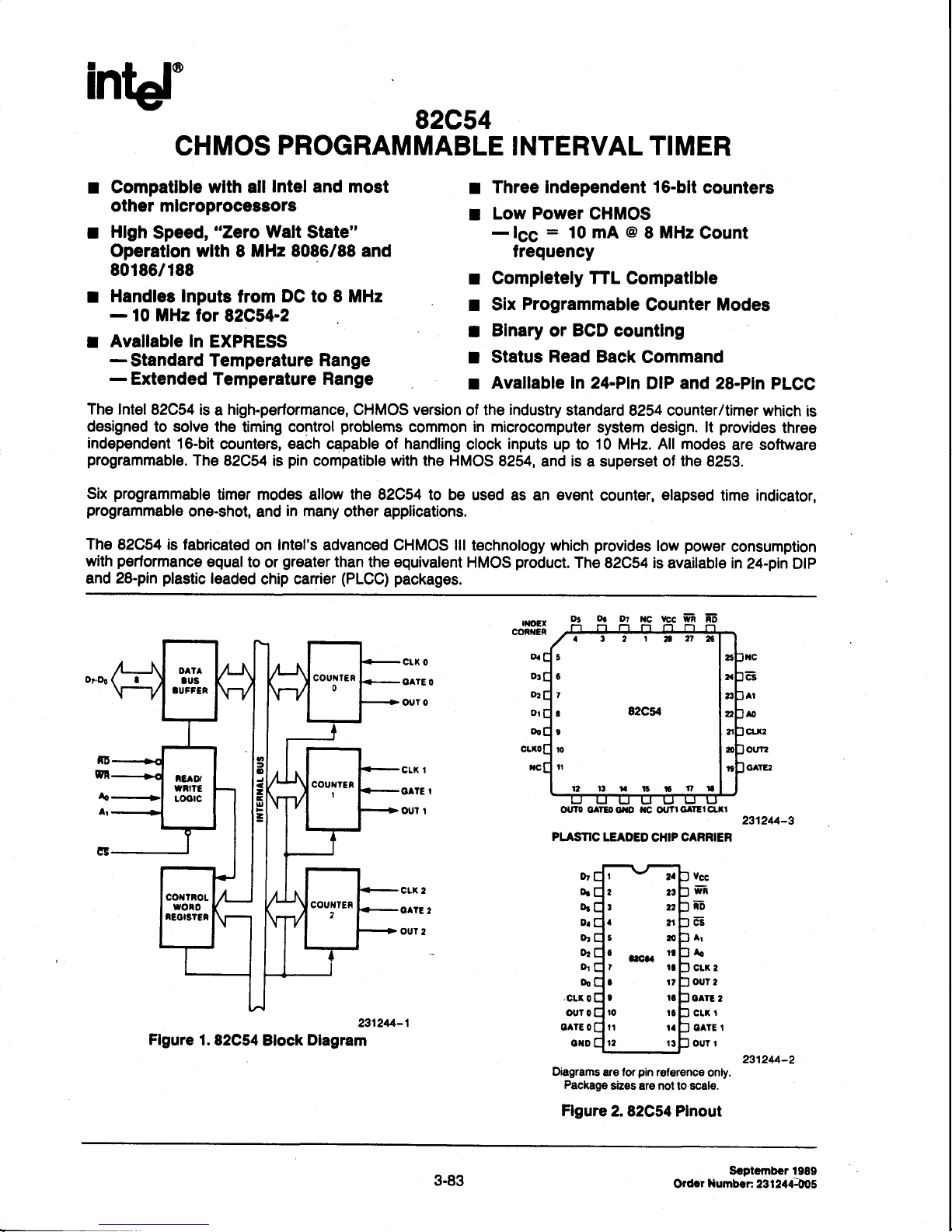
intel'
CHMOS
Compatlble wlth all
r
other mlcroprocessors
Hlgh
r
Speed,
"Zero
Operatlon wlth 8
80186/188
Handles Inputs
I
-
10 MHz for
Avallable In
r
-
Standard Temperature Range
-
Extended
The Intel
designed
independent
programmable.
Six
programmable
The
with
and 28-pin
82C54 is a high-performance, CHMOS version
solve
to
16-bit
programmable
82C54 is fabricated
performance
plastic
82C54-2
EXPRESS
Temperature
the
counters, each capable of handling
The
82C54 is
timer modes allow the 82C54 to
one-shot,
equalto
leaded
Intel
Walt
MHz 8086/88 and
from
timing
and
on
or
chip
82C54
PROGRAMMABLE
and most
State"
DC to 8 MHz
Range
control
pin
in
Intel's advanced CHMOS lll
greater
problems
common in microcomputer
compatible with th€ HMOS
be used
many
other applications.
than
the equivalent
carrier
(PLCC)
packages.
INTERVAL
Three Independent 16-blt
I
Low Power CHMOS
I
-
lcc : 10 mA
frequency
Completely
r
Programmable
Six
r
Blnary or BCD countlng
I
Status
I
Avallable In 24-Pln
I
industry
of the
inputs
clock
8254,
and
as an
technology which
HMOS
product.
TIMER
o
MHz
8
TTL
Compatlble
Counter
Read Back
standard
up to 10 MHz. All
is
a superset
6vsnt
The 82C54
Command
DIP and 28-Pln
8254 counter/timer
system
counter,
provides
design.
elaps€ct
low
is available in
Count
modes
of the
power
counters
Modes
PLCC
which
provides
lt
are software
8253.
time indicator,
consumption
24-pin
is
three
DIP
Flgure
1.82C54
Block
2312U-1
Dlagram
OIOCI
coiilEn
Oa
Dt
Or
Ot
DO
6
,
I
9
t0
lt
t2lt'.ts$?ll
oalEocaao xc
PLASNC
O,
Or
Or
D.
Dr
Ot
Dr
Oo
.cLx
0
out 0
OAIE O
or{D
Diagrams
Package
Ffgure
LEADED
I
2
3
a
5
t
I
a
c
t0
It
l2
ar€ lor
sizes
CAFRIER
CHIP
2a
tt
t2
21
20
rt
ra
rt
!3
rt
ta
'|l
pin
reterenc€ only.
not
ar6
to
Ycc
m
m
d-s
At
Aa
cLr 2
oul
OATC
cLx
CATE T
ouT t
scal€.
2.82C54 Plnout
c3
AI
AO
c|.x2
23124/--3
2
2
r
231244-2
3-83
Ordcr
scPtGmbor 1989
Numbcn
231244405
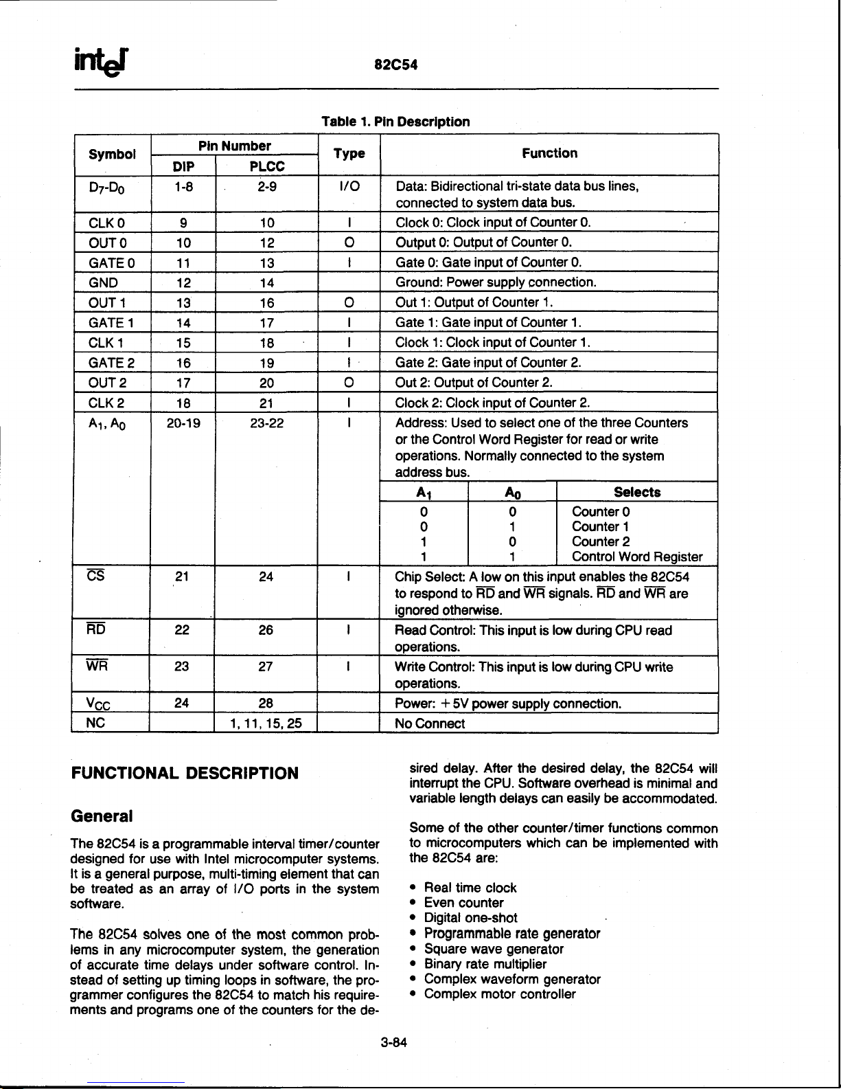
int€f
82C54
Symbol
Dz-Do
O 9
CLK
OUT O
GATE O 11 13
GND 12 14
1
OUT
1 14 17
GATE
1 15 18
CLK
GATE 2
2 17
OUT
2
CLK
Ar, Ao
G
m
WF
Vr:n
NC
Pln Number
DIP
1-8 2-9
PLCC
10 Clock
10 12
13 16
16
t9
20
18 21
20-19 23-22
z',|,
22
23
24
24
26
27
28 Power:
1, 11, 15,25
Table 1.
Pln Descrlption
Type
vo
o Output
o Out
I
o Out 2:
I
I
I
I
Function
Data: Bidirectionaltri-state
connected
Gate 0: Gate
Ground:
to system data
0: Clock
input of Counter 0.
0: Output of
input
Power
supply
Counter 0.
of
1: Outpui of Counter
Gate 1: Gate
Clock
2: Gate input
Gate
Clock 2: Clock
inout
1:
Clock
Output
of Counter
input
of
Gounter 2.
of
inout
Address: Used to select
the Control Word Register
or
operations.
Normally
data bus lines,
bus.
Counter 0.
connection.
1
Counter 1.
of
Counter 2.
of Counter
one
connected
address bus.
Ar Ao
0
0
1
1
Chip Select A low
to respond to FD
iqnored
Read
otherwise.
Control:
and
This
0
1
0
1
input enables
this
on
WFi signals. RD and WFlare
input is
low during
operations.
Write
Control: This input is
low
operations.
power
*
5V
supplv
connection.
No Connect
1.
2.
the three
of
for read
to the
Gounters
write
or
system
Selects
Counter
Counter
0
1
Counter 2
ControlWord
the 82C54
CPU
during GPU
Reqister
read
write
FUNCTIONAL
DESCRIPTION
General
The
82C54 is
designed for
generalpurpose,
It is
a
be treated as
software.
The
82C54 solves one
lems
in
any
of accurate
stead of setting up timing
grammer
ments
and
programmable
a
with Intel
use
multi-timing
an anay ol
microcomputer
time
delays under software control. In-
intervaltimer/counter
microcomputer systems.
element
ports
llO
the most
o{
system, the
loops in
software,
configures the 82C54 to match
programs
one of the counters for the
that
in the
system
common
generation
the
his require-
can
prob-
pro-
de-
sired delay.
intenupt
variable length
Some
to microcomputers
the 82C54
r
Realtime
o
Even
o
Digital
o
Programmable
.
Square wave
o
BinaU rate multiplier
o
Complex waveform
o
Complex motor
After
the
the CPU. Sottware overhead is minimal
delays can
the
of
other counter/timer
are:
clock
counter
one-shot
rate
generator
controller
desired
which can be implemented
delay, the 82C54
easily
be accommodated.
functions
common
generator
generator
will
and
with

intef
82C54
Block Dlagram
DATA
This
terface
BUS BUFFER
3-state, bi-directional, 8-bit butler
the 82C54 to the
system bus
is
used to in-
(see
Figure
3).
CONTROL WORD REGISTER
The
ControlWord
by the Read/Write Logic when
CPU then
data
interpreted
operation of
The Control Word
status
Command.
does a
is stored in the Control
information
ND
m
Register
write operation
Control
as a
the
Counters.
Register can
is
(see
Word Register
Word
available
Figure
4)
is
selected
Ar, Ao : 11.
to
82C54,
the
used to define
only be
with
written
the
Read-Back
lf
the
the
and is
the
to;
Flgure
3.
Buffer
Block
and Read/Wrlte
READ/WRITE
The
Read/Write
tem
bus and
functional
generates
blocks
one of the three
ter to
input
the
82C54
or
6; HE
been selected
read
be
tells
the 82C54
counters. A
that the CPU
initial
an
count. Both
and WH
from/written
by holding
Dlagram
LOGIC
Logic
accepts inputs from
control
of the 82C54.
counters
or the
into. A "low"
that
the CPl.l is
"low"
on
is writinq
FiD
anO
ignored
are
CS low.
231244-4
Showlng
Loglc
signals
Data
Functlons
for
A1 and As
Control
Word
on the FiD
reading
the
WH
input
either a Control
Wn-
unless
qualified
are
the
82C54
Bus
the
the
ReE
one
tells
sys-
other
select
of
the
Word
by
hai
Flgure
4. Block
Reglster
couNTER
These
three
tion,
so only
internal
in
The
may
The
is
termine
block
Figure
5.
Counters
operate
Control
part
not
how
Dlagram Showlng
and
Gounter
O, COUNTEB 1,
functional
blocks are identical
a single Counter will
diagram
fully
are
in a different
Word
Register is
the
of
Counter
the Counter
single
of
a
independent.
Mode.
itself,
operates.
231244-5
Control
Functlons
COUNTER
be
2
described.
counter
Each
shown
in the
but its
contents
Word
in
opera-
The
is
shown
Counter
figure;
de-
it
3-85

int€t
82C54
status
Internal
register,
Flgure 5.
The
latched, contains the
Word Register
flag.
count
Back
command.)
The
actual
ment").
lt is a 16-bit
and status
(See
detailed explanation of
counterls labelled CE
counter.
Dlagram of a Counter
Block
shown
current
in the Figure, when
contents
of the output and
(lor
presettable
synchronous down
231244-6
the Control
of
the Read-
"Counting
Ele-
null
CR and
in the
stored
Control
loaded
ferred to the
cleared
way,
byte
significant
Note that the
count
The Control
n,
side world
82C54
The 82C54
array of
the
Logic allows
from
when
if the
counts
is written,
GATE n,
SYSTEM
peripheral
fourth
the internal
CE simultaneously. CRy and CRl
the Counter
Gounter
(either
byte onty) the other
CE
Logic
and OUT n are
through the Control Logic.
is treated
control
is a
ming.
Basically, the
A1
address
select inputs
bus signals
derived directly
method.
select
of a decoder,
Or
such as an
t€ms.
later transferred
register
one
Both bytes
bus.
is
has
been
most
significant
to
at a
programmed.
programmed
byte
byte will
cannot be
written
into; whenever
it is written into the CR.
is
also shown
in
the diagram. CLK
connected to the
all
INTERFACE
by the systems
ports;three
l/O
register for MODE
A0, A1 connect
the
of
from the
address
it
can be connected to
Intel
software
are counters
The
CPU.
bus using a linear
8205
for
the CE.
The
time to be
trans-
are
ln
for
one
only or
least
be zero.
out-
as an
and
program-
to the
CS can be
the
output
larger
sys-
are
this
a
A9,
OLy and
"Output
"Most
OL1
are
Latch";
significant
the subscripts M and
byte" and
respectively. Both
just
the
called
CE,
but
unit and
low"
two
are
OL.
if
a suitable
latch€s.
8-bit
"Least
normally
OL stands
significant byte"
referred
These latches normally "fol-
Counter
Latch.Command is sent to the 82C54, the latches
present
to
count until
"following"
by the counter's Control Logic
bus. This
over the
cannot
the OL
Similarly,
and
is how the 16-bit Counter communicates
8-bit
read; whenever
be
is
that
there
(for "Count
CRg
relerred to as one unit
new
count
is written
read
the CE.
internal
read.
being
two
are
the
CPU
by
latch at a time
One
to
Note
bus.
8-bit
Register").
and
to the
that the CE itself
you
read
registers
Both
called
Counter, the
and
ddve the
the count,
called
are
CR.
iust
for
as
for
on€
the
L stand
to
"latch"
then return
is
enabled
internal
it is
GBtul
normally
When a
count
is
lo
Ar
Cl
.
coutttt
0r
r--:*
out olTC
cLt
Flgure 6.
DlD,
atcaa
corrtl:t
r-:+
'ot
t
oalc
crx'
'ot
82C54 System
couxt:i
l
otlE clx
231244-7
Intertace
3-86

intef
82C54
OPERATIONAL
DESCRIPTION
General
power-up,
Atter
The Mode,
undefined.
are
How each
programmed.
before
programmed.
it
can
the state
value,
count
Counter
Each
used.
be
of
and output
operates
Counter
Unused counters need not be
ControlWord Format
A1,A9:11 G:O
ffi:1
the 82C54 is
is
determined when it is
must
undefined.
of
Counters
all
programmed
be
WH:O
D7 D5 D5
scl
sc0 RW1 RWO
Programming
Counters
then
and
shown in Figure 7.
All Control Words are written
Register, which
ControlWord itself
programmed.
By contrast, initial
ters,
not the
puts
are used
into. The format
the ControlWord used.
Da
D3 D2
M2 M1
programmed
are
initial count. The
an
is
Control
to
of the initial
D1
MO BCD
the
82C54
by writing
selected
when
specifies
counts
select
are written
Word
Register.
the Counter
Ds
a ControlWord
control word format
into
the
Oontrol Word
41,
which
count is
:
11.
Ao
Counter is being
into
the Coun-
The
41, A9 in-
to
written
be
determined
is
The
by
-
SC
Select Counter:
scl
0 0
0 1
1 0
1
-
RW
RWl
NOTE:
compatibility
Read/Wrlte:
RWo
0
0
1
0
1
0
1 1
Don't
sco
Select Counter
Select
Counter
Select
Counter
1
Counter Latch Command
Operations)
Read/Write
Read/Write most
Read/Write least
most
then
bits
care
with
future
Read-Back
(See
least
significant
(X)
should
products.
Intel
Read
Operations)
significant
signilicant
significant
byte.
be 0 to insure
0
1
2
Command
(see
Read
byte only.
byte only.
first,
byte
Figure
7.
-
M
n2 Ml
0 0
0 0
X
x 1
1
1 0
BCD:
0
1
GontrolWord
MODE:
1
0
Binary Counter
Binary Coded Decimal
(4
Decades)
Format
MO
0
1
0
1
0
1
16-bits
Mode 0
Mode 1
Mode
Mode 3
Mode
Mode 5
(BCD)
Counter
2
4
3-87

iilef
82C54
Wrlte
The
flexible.
Operations
programming procedure
two conventions need
Only
bered:
1) For
written
2) The
specified
byte only, most
nificant
Since
the
Counters have
Ar, Ao inputs),
Counter it
ControlWord
LSB of count
Counter,
each
before
the initial
initial count must tollow
in
the Control Word
significant byte
byte and then most significant
Control Word Register
separate
and each Gontrol
applies to
-
-
MSBofcountControl Word
LSB of
MSB
of count-
Control
-
count - Counter 1
-
Word
LSBofcount-
MSB
of count
-
for
the Control
count
addresses
(SC0,
SC1
Counter 0
Counter 0
Gounter0
Counter 1
Gounter 1
Counter 2
Counter2
Counter
the 82C54 is very
to be remem-
Word must
written.
is
the count format
(least
significant
only, or
least
byte).
the three
and
(selected
Word
by
specifies
bits), no special
41 Ae
11
00
00
11
01
01
11
10
2
10
be
sig-
the
the
in-
struction
sequence
s€quence is required.
that follows th€
conventions
ceptable.
A new
any
grammed
as
must
initial
time without affecting
Mode in
described
follow
the
lf a Gounter
counts, the
must
following
not
transfer control
and second byte to another
into that
be
same Counter.
loaded with
ControlWord
Control Word
ControlWord
LSB
of count
MSB of countLSB of count
MSB
of countLSB of count
MSB of
count
may
count
way.
any
in
the Mode
programmed
programmed
is
precaution
Othenrise,
incorrect
an
-
Counter
-
Counter
-
Counter
-
Counter
Counter
-
Counter
Counter
-
Counter
-
Counter
be
Counting will
definitions.
between
routine
programming
Any
above
written
to
the
Counter's
a Counter
The new
count format.
read/write
to
applies:
writing
which
the
count.
A1
'l
2
1
1
1
0
1
2
2
1
1
0
1
0
0
0
0
0
is
ac-
at
pro-
be
atfected
count
two-byte
program
A
the first
also writes
Counter will
Ao
1
1
1
0
0
1
1
0
0
Control Word
Counter Word
Control Word
LSBofcountLSBofcountLSBofcountMSB
of count
MSB
of count - Counter
MSB
of count - Counter
-
Counter 0
-
Counter 1
-
Counter
Counter2
Counterl
Counter0
-
Counter
NOTE:
ln
four examples,
all
These
are only
Read
It is
without
ly
There
Operations
often desirable to read the
disturbing
in
done
are three
four
the 82C54.
counters
all
many
of
the
count
possible
counters: a simple read
2
0
1
2
possible
Figure
programming
8. A Few Poeslble
programmed
are
value
progress.
in
methods
for
operation,
A1 Ae
11
11
11
10
01
00
00
01
10
a Gounter
of
This is
reading
the
Counter
to read/writ€
saguenc€s.
Programmlng
form
easi-
which
input
using
the
wise,
when
ControlWord
-
ControlWord-
LSB
of
ControlWord
LSB
of count
MSB
of count-
count
-
-
-
LSB of countMSB
of count-
MSB
two-byt€
of count
counts.
-
Sequences
Latch Command,
Each is
explained
and the
below.
a simple read
is
selected
with the
of the selecied
either the
the
it is read,
GATE inpui
count may be
giving
Counter
Counter
Counter
Counter
Counter
Counter
Counter
Counter
Counter
Read-Back
The first
operation.
To read
A1,
Counter
an
must
external
or
process
in
the
undefined
A1 A6
1
11
11
0
1
01
2
11
0
00
1
01
10
2
0
00
10
2
Gommand.
method
the
A0 inputs,
be inhibited
logic.
of changing
result.
per-
is
to
Counter,
the
CLK
by
Other-
3-88

intef
82C54
COUNTER
The
second
mand".
to the
when
SCO, SC1
two
from
Like
Control
41,
Ao
bits select
other
bits,
a ControlWord.
Al,
AO:11;
D7
sc1
SC1,
D5
sc0
SCO
-
scl
0
0
1
1
-
D5,D4
X
NOTE:
Don't
with
-
don't
future
00
care
care
bits
Intel
LATCH
method
a Control
COMMANO
uses the
Word, this
Word
:
11.
Also like
one
D5
and D4,
6:0;
specify
RD-:1;
D5
0
counter
sco
0
1
0
1
Read-Back
designates
(X)
should
products.
"Gounter
command
Register,
which
a Control
of the three
distinguish
WF:O
Da D3
0tx
to be latched
Counter
0
1
2
Command
Counter
be 0 to insure
Latch
Latch
is
Word,
Counters,
this
command
D2 D1
X X
Command
compatibility
Com-
written
is
selected
the
but
Ds
X
gramming
serted between
Another
writes
example,
counts,
lf
a Counter is
counts,
must
and second
from
count will
READ.BACK
The
This
value,
OUT
ter(s).
The
command
ister
command
ting
their
operations
feature
of the
same Counter
if
the Counter
the following
'1.
Read
Write
2.
3. Read
4.
Write
following
the
not
transfer
byte to
that
same
read.
be
third
method
command
programmed
pin
and Null
and has
applies
corresponding
of other Counters
them.
of the
is
sequence
least
significant
new
least
significant
most
significant
new
most
programmed
precaution
control
another
Counter.
COMMAND
uses
the
allows
is written
the format
the
Mode,
Count
flag
into
to the
counters
bits DB,D2,D1
82C54
significant
between
shown in
is
that reads
may
programmed
be interleaved:
is
valid.
byte.
byte.
byte.
byte.
readlwrite
to
applies;
reading
routine
Otheruvise,
user
and
which
Read-Back
to
check the
current
the
of
selected
the
Control
Figure
selected
may
be
for
two
two-byte
program
A
the
reads
also
incorrect
an
command.
count
state
of the
coun-
Word
10.
by
:
1.
in-
and
for
byte
first
Reg-
The
set-
Figure
The
count
received.
by the
The
OL
This
:'9!
Multiple
latch
ter's
Commands
the
lf
a Counter
latched
Counter
will
Command
With
ing
Counter
bytes
read
9.
selected
at the time
This
CPU
count
returns
allows reading
the
fly"
Gounter
more
OL holds
Counter
again
Latch
be
the
was
either
to
the
is
must
one right
Counter
Counter's
(or
is
then
"following"
to
without
than
its
do not
in
is latched
before
Command
count
method,
programmed
programmed
be read. The
Latchlng
the
count is
until the
unlatched
the
atfecting
Latch
one
Counter.
count
affect
any way.
the
at the
issued.
the
after the
held
Command
output tatch
Counter
Counter
the
contents
Commands
until
and then,
count is read,
is
time the first
count must
format;
for
two
other; read
Latch
in
the latch
is reprogrammed).
automaticaliy
counting
counting
Each
it
is
read.
programmed
the
some
ignored.
specifically,
two
byte
bytes
do
oi the
be read
Format
(OL)
latches
Command
until it
element
progress.
in
miy
be
latched
Counter
time later,
the
The
count read
Counter
counts,
not
have
write
or
the
is
is read
and the
(CE).
Counters
used
to
Goun-
Latch
Mode
of
second
Latch
accord-
if
the
two
to be
pro-
or
A0,A1
D5: 0
Da:0
D3:
D2: 1
Dr: 1
Dg:
The
S_pgnter
COUNT
te(s).
lent
each
is held
grammed).
when
they
are issued
:11
D7
1 1
6TNT
:
Latch
:
Latch status
:
1
Select
=
Select
:
Select
Reserved
Figure
read-back
bit D5:0
This
to
several
counter
until it
read,
read.
are
Q$-O
count
counter
counter 1
counter
for luture
10.
Read-Back
command
output
single
counter
latched.
is
That
counter
but
other
lf multiple
to
the
FD:1
Da
SlTr-US
and
command
read
same
CNT2
ol selected
of selected
2
0
expansion;
may
latches
selecting
latch
Each
(or
is
counters
count read-back
counter
WF:o
CNT 1
CNTO
counter(s)
counter(s)
must
be 0
Command
be
(OL)
is functionally
commands,
counter's
the
automatically
remain
without
Format
used
to latch
by
the
desired
latched
counter
latched
setting
commands
reading
D1
0
multi-
the
Loun-
equiva_
one
for
count
is
repro-
unlatched
until
the
3-89

inbf
82C54
count,
which
read-back
but the first
all
will
be read
command
The read-back
information
status
ffifre
read;
that
The
D5
Mode
Word.
the
counter's
bit D4:0. Status
status
of a counter is
counter.
counter
through
status tormat
D0
exactly
as
OUTPUT
pin.
OUT
This
output via
some hardware
OUTPUT
Dz1:OutPinisl
0: OutPinis0
D5 1:
0
Ds-Do Counter
NULL
COUNT
written
into
happens
described
is loaded
read
before
new
is
to the
the
from
this
count
shown in Figure
NULL
COUNT
Null
count
:
Count
Flgure
bit DO
counter
counting
depends
in
the Mode
into
the
the
counter.
time, the
just
written.
are
is
the
count
was
issued.
command
may
of selected
is
contain
bit
the
written
D7
contains the
in
allows
software,
from
a system.
RWI
available
element
counting
for reading
Programmed
11.
Status Byte
indicates
register
(CE).
on
the Mode
Definitions,
lf
the
count value
The
12.
ignored;
i.e.,
the count
at the time the
also be used to latch
counter(s) by
must
be tatch6d
accessed
by a read from
shown in Figure 11.
counter's
programmed
the last Mode
cunent state
the
user to monitor the
possibly
Dl
RWO
M2 M1 MO
Mode
when
(CR)
The
of
the counter
but
element
count is latched
will not
operation
eliminating
(See
Figure
the last
has
been loaded
exact time this
untilthe
(CE),
it
can't
reflect
of Null Count
first
setting
to ue
Bits
Control
of
BCD
7)
count
and is
count
be
read
or
the
THIS
ACTION:
A. Write to the
word
B. Write to the
r"tot"i
C. New
into
ttl
have its null
counters
l2l
(least
count
the
Qn!
are unatfected.
f
tne counler is
significant
goes
control
register:ht
count
tcnitri
is loacled
count
+
(cH
cE
counter
count
byte thgn
to 1 when the
Flgure 12. NullCount
lf multiple
are
first
the status
read-back
Both
may
ffi
tionally
commands
ply
here
status read-back
counter(s)
first
lf
both
first read
status latch
performed
without
are ignored;
of the
command was
count
and
be latched
and SIAluS-
the same
at once, and the
Specifically,
also.
without
are ignored.
count
This is illustrated
and status
operation
i.e.,
counter
status
simultaneously
as
commands
any
status, regardless
next
one or two reads
counter
return
latched
programmed
is
latched
count.
count.
6E;.
specilied
set to 1. Null
programmed
by
most
second
operations
reading
the
status
the
at
issued.
of the
bits DS,D4:0.
issuing
two separate
above
if multipl€
are issued
intervening
of a counter
that
of
counter
of which
was latched
(depending
for
one or two
Subsequent
CAUSES:
Null
count= 1
Nullcount:1
Null
count=o
the
control
count bits
for
two-byte
significant
written.
byte is
Opera$on
of the
the
status,
that will
time
the
selected
by setting
rnis
discussions
count
to
reads,
in Figure
are
latched,
will
return
on whether
type counts)
reads
word
will
of other
counts
byte) null
counter(s)
all but the
be read
first
is
status
counter(s)
both
ii func-
read-back
ap-
and/or
the
same
all but
the
13.
the
latched
first. The
the
return
un-
Command
D7 D5
1 1
1
1
1
1
1
1 1
1 1
1
1 0
1 1
D5 Da
0 0
0
0
0
1 1
0
0
D3 D2
0 0
1
0
1 1
0
1
0
0 0 1
D1
1
0 0
0
0
0
Figure
D9
0 Read
back
Counter
Read
back
0 Read
0 Read
0 Read
back
back count
back
Counter
0 Read
back status
13. Read-Back
DescrlPtlon
count
0
status
status
count
1
Gommand
3-90
and
status
of
of Counter 1
of Counters
of Counter
and status
2
of
of Counter
Example
Count
for
Status
2, 1
status
2,
Count
Count
but not
1
Command
already latched
Results
and status latched
Counter 0
latched
latched
but not
latched
latched lor
status
for
for
Counter
for
ignored,
for
Counter
counter
1
Counter
Counter 1
2
status
Counter 1
1

inqef
cs RD WR
0
1
0
1
0
1
0
1
0
0
0
0 1
0
0
0
0
1
x
X
0 1
Flgure
14.
Ar
Ao
0
0
0
0
0 1
0 1
0
'l
1
1
1
1
0
0
1
1
X
X
0
1
0 Read
1
0
1
X
X
Read/Wrlte
Write
into
Counter
Write
into
Counter
Write
into
Counter
Write
ControlWord
from
Counter
Read
from
Counter
Read
from
Counter
No-Qperation
No-Operation
No-Operation
Operailons
Summary
0
1
2
0
1
2
(3-State)
(3-State)
(3-State)
82C54
goes
CLK
already
This
allows
ed
by^gottware.
+
lf
an
still
pulses
1
CLK
initial
be loaded
high,
OUT witt
pulse
is needed
been
the
counting
Again,
afier the
count
on the
done.
sequence
OUT
new
is written
next
CLK
go
high
to load
does
count
while
pulse.
N
CLK
the
Counter
to
be
go
not
ot tt
GATE
When
putses
synchroniz_
high
untit
N
is written.
:
0, it
will
GATE
tater;
no
as this
has
Mode
The
Definitions
following
operation
CLK PULSE:a
TRIGGER:
COUNTER
MODE
Mode
Control
remain
goes
new
0: INTERBUPT
0 is
typically
Word
low
high
and remains
Mode
ter.
GATE
counting.
After
a Counter,
CLK
count,
high
:
1
GATE
the
Control
the initial
pulse.
so for
until N +
written.
ll
a new
loaded
tinue
ten,
1)
Writing
low
2) Writing
count
on the
from
the
the
following
the first
immediately
the
be loaded
are
defined
of the 82C54.
rising
edge,
that
order,
rising
a
edge
put.
LOADTNG:
ON TERMTNAL
used for
is
written,
untilthe
Counter
high
0
Control
enables
Word
counting;
has
no
Word
etfect
and initial
count
CLK
1
CLK
is
written
pulse
count
putses
pulse
CLK
count.
This
an initial
next
new
happens:
byte
disabtes
(no
clock
second
on the
byte
next
for
use
in
describing
then
of
a Counter,s
of
a
the
transfer
the
CR
failing
a
Counter's
of a
count from
to
the
CE
the "Functional
tion")
COUNT
event
countinq.
OUT is initially
reaches
until
is
written
GATE
on
count
will
be
does
of
N,
after
to
the
and
lf
a two-byte
counting.
pulse
allows
pulse.
CLK
lo-w,
zero.
a new
count
into
:
0
OUT.
are
loaded
not
on the next
decrement
OUT
does
the initiat
Counter,
counting
count
OUT is
required).
the
new
the
edge,
in
CLK input.
GATE
in-
(refer
to
Descrip-
After
the
and will
OUT
then
or a
the
Coun-
disables
written
to
the
go
not
count
is
it
will
be
will
con.
is writ_
set
count
to
3-91
l"
l"l-l*l*
NOTE:
The
Following
Diagrams:
1.
Counters.
golllins
(LSB)
only.
2. The
counter
3.
CW
stands
control
word
4.
LSB
stands for
5.
Numbers
The
lower
The
upper number
the
counter
the
most
N
stands for
Vertical
lines
-l
|
l*
|
"
CW.l0
t!!rt
l-
l-
l- l3lt
Conventions
are_programmed
and for
signilicant
Reading/Writing
is
always
"Control
for
10,
of
hex is
"Least
below
number
diagrams
is
the
is the
is. programmed
byte
an undelined
show
transitions
Figure
*
I
|
!
I
l3
l:
Apply
selected (G
Word";
written
Significant
are
least
signiticant
most
to
cannot
count.
between
15.
Mode
I I I i
lt
I I
for
count
signilicani
Read/Write
be read.
l!
ll
To
binary
teast
CW
to the
Byte"
0
I
i?
lt
All
signiiicant
always
:
counter.
values.
byte.
count
s
lfflF[l
ls lr:l
l;
lt:l
231244-8
Mode
Timing
(not
low).
iO
mein"
of count.
byte.
Since
LSB
values.
BCD)
byte
a
only,

intef
HARDWARE
IIIODE
ONE-SHOT
OUT
pulse
and
QUT
pulse
After
Counter
Counter and
thus starting
will
tion.
remain
one-shot
same count
OUT.
shot
less the
Counter
shot
1:
be
will
following
remain
will
then
will
atter
writing
is
result
The one-shot
low
new count
ll a
pulse,
is loaded
pulse
the
armed.
in a
pulse
Counter
continues
RETRTGGERABLE
OUT
initially
for N CLK
high.
trigger
a
low
go
next
the Control
setting
to begin
the
until
high and
trigger.
Word and
trigger
A
OUT
low
the one-shot
one-shol
pulse
retriggerable,
is
pulses
repeated
be
can
remain
pulse.
into the counter.
written to
is
the current
is
the
one-shot
retriggered.
with the
the
until
go
will
the
Counter
high
results
the
on
An
N
CLK
after
without
GATE
Counter
is
In
count
new
new count
low on
one-shot
reaches
untilthe
initial
in
next
initial
cycles
hence
any
pulse,
zero.
count,
loading
pulse'
CLK
count
in dura'
OUT
trigger.
CLK
CLK
the
rewriting
etfect
no
has
a
during
not affected
case,
that
the one-
and
expires.
82C54
the
the
N
of
will
The
the
on
one-
unthe
MODE
This
typicially
rirpt.
2:
Mode
used
OUf
functions
generate a Real
to
initially
will
GENERATOR
RATE
has decremented
pulse.
ioads
Mode
indefinitely.
repeats
GATE
counting.
OUT
Counter
OUT
GATE
the
OUT
initial
the
is
2
every
:
1 enables
lf GATE
is set
with the
goes
then
count
periodic;
For an
N CLK
immediately.
high
initial count
N CLK
low
input
Counter.
N CLK
also.
Control
loaded on
Pulses afier
the
writing a
After
Counter
low
ooes
This allows
ien.
software
wili be
like a
be
1, OUT
to
goes
high again,
and
same
the
initial
cYcles.
counting;
goes
pulses
be
can
Counter
divide-by-N
When the
high.
goes
process
the
sequence
of
count
GATE
during
low
A trigger
the next CLK
on
after
to synchronize
used
Word and
next CLK
the
initial count
the
to be
counter.
inter'
Clock
Time
count
initial
for one
low
Counter
the
is repeated'
repeated
is
N, the
sequence
:
0 disables
an output
pulse,
reloads
pulse;
the trigger.
initial count,
pulse.
is
synchronized
lt is
CLK
re-
the
Thus
the
the
OUT
writ-
by
w-t
ctx
oArc
oul
WF
clx
oltE
our
9F
crx
Gltt
our
l- i.
xlr
I
Figure
ir I
16.
I
i : l3i:[lffl:
1
Mode
l3
231244-9
WF
cl(
oltt
out
WT
clx
o^lE
oul
il:
ll
ll
l-l:
l-
l,.l-
lElra
Cwrll
.Wr
cLx
GATE
our
l-1.1.1.1:
|
NOTE:
A GATE
terminal
transition
count.
should
Flgure
not occur
17. Mode
l3
LSl.5
l3i:
I
ll
ll lll:l3l
one clock
2
I
231244-'.lo
prior
to
3-92

inbf
82C54
Writing
the
cunent
ceived
of the
cunent
the
new
will
continue
new
count will
counting
MODE
Mode
3 is
Mode
3 is
of
OUT.
tial
count
der
of
the
above
is repeatad
results
cycles.
GATE
:
coulling.
set
high
trigger
reloads
the next
used
to
Atter
writing
Counter
allows
the
also.
Writing
the
ceived
of the
a new
current
after
cunent
Counter
next
CLK
new
count.
at the
end
Mode
3 is
Even
counts:
loaded
by two
expires
loaded
on
on
OUT
with
repeated
Odd
counts:
minus
one
pulse
and
ing
pires,
with
pulses
expires,
reloaded
process
pulses.
CLK
OUT
the
initial
decrement
OUT
with
is repeated
new
a
count
counting
after writing
a new
period,
count
cycle. In
3:
SQUARE
typically
similar
OUT
has
count.
the
on
from
the
loaded
be
mode
WAVE
used
to
Mode
wiil
initialty
expired,
Mode
indefinitely.
in
a sguare
1
enables
lf
GATE
wave
counting;
goes
immediately;
the
Counter
pulse.
CLK
synchronize
Thus
the
a Control
will
be loaded
Counter
to
count
while
counting
writing
a new
half-cycle
will
be loaded
pulse
and
counting
Otherwise,
of the
current
implemented
OUT
is initially
CLK
initial
pulse
CLK
value
count.
one
succeeding
changes
the
indefinitely.
OUT is
(an
then
goes
goes
the
initiaily
even
number)
is
decremenled
One
CLK
low
and the
count
minus
the
count
high
initial
count
indefinitely.
while
counting
sequence.
count
the
Counter
next
CLK
new
count.
at
the
2,
a COUNT
MODE
for
Baud
2
except
be high.
goes
OUT
3 is-periodic;
An
with
a
GATE
low
white
OUT
CLK
with
the
pulse
the
GATE
no
Counter
Word
and initial
on the
be
next
synchronized
counting
sequence.
count
of the
with
the
new
but
square
the
new
will
continue
count
lf
half-cycle.
as follows:
high.
The
and then
pulses.
and the
The
above
high.
is loaded
by two
gulse
after
Counter
one.
Succeeding
by
two.
again
and
minus
So for
does
not
lt
a
trigger
but
before
will
be
pulse
loaded
and
Othenvise,
end
of
the
of
1 is
qeneration.
rate
for
thJduty
When
hatf
low
for
the remain-
the
sequence
initial
count
period
of N CLK
=
0
is
tow,
is
required.
initial
count
disables
input
count,
pulse.
CLK
by
software
does
not
a
trigger
befo-r6
the
wave,
count
lrom
will
be loaded
initialcount
is
decremented
When
the
Counter
process
The
initiat
on one
on succeed_
the
count
is reloaded
When
the
the
Counter
one.
The
odd counts,
atfect
is
re-
the
end
with
counting
th6
current
illegal.
cycle
ina
ini_
of N
OUT
is
A
on
can
be
the
This
atfect
is
re-
end
the
on the
the
is
count
is re_
is
count
CLK
ex-
CLK
count
is
above
OUT
will
-1)/2
(N
m
ctl
orra
0t
9t
c!i
oAr:
our
9I
cu
olt:
oul
l-l.l*l.i:
NOTE:
A
GATE
l€rminal
IIODE
OUT
pirgq,
go
by writing
GATE
counting.
Atter
Counter
CLK
initial
N +
ff
loaded
tinue
ten,
high
new
a
the
pulse
1
from
4:
will
OUT
again.
:
writing
will
count
CLK
count
on the
following
be high
for
counts.
l:l :i:i
transition
count.
SOFTWARE
be initiaily
will
the initial
1
GATE
does
the
should
Flgure
high.
go
low
The
counting
count.
enables
counting;
has
no
a Control
be loaded
not
decrement
of N,
is
wriilen
next
new
OUT
after
GLK
count.
pulses
happens:
(N
+
1)/2
counts
Itl:l:
not
occur
one
18.
Mode
3
TRtccERED
When
the
for
one
CLK
s€quence
GATE
effect
on
OUT.
Word
and initial
on the
does
the
initial
during
pulse
lf
a
next
CLK
the
couni,
not
strobe
count
counting,
and
countiig
two-byte
and low
!l
l|
231244-11
prior
clock
to
STROBE
initiat
count
and
ex-
then
pulse
is,.triggered,,
:
O
disables
count,
pulse.
is
corjnt
the
This
so for
an
iow
until
written.
it
wilt
be
wiil
con_
is
writ
for
3-93
 Loading...