

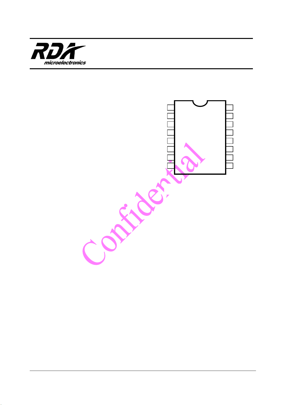
Figure1-1. RDA5807FP Top V i ew
RDA5807FP
1
2
3
4
5
6
7
8
16
15
14
13
12
11
10
9
GPIO2
GPIO3
GND
ROUT
LOUT
RCLK
VDD
GND
GPIO1
GND
RF GND
FMIN
GND
GND
SCLK
SDA
RDA5807FP
SINGLE-CHIP BROADCAST FM RADIO TUNER Rev.1.2–April.2012
1 General Description
The RDA5807FP series is the newest generation
single-chip broadcast FM stereo radio tuner with fully
integrated synthesizer, IF selectivity, RDS/RBDS and
MPX decoder. The tuner uses the CMOS process,
support multi-interface and require the least external
component. The package sizes is SOP16. It is
completely adjustment-free. All these make it very
suitable for portable devices.
The RDA5807FP series has a powerful low-IF digital
audio processor, this make it have optimum sound
quality with varying reception conditions.
The RDA5807FP series support frequency range is from 50MHz to 115MHz.
1.1 Features
CMOS single-chip fully-int egrated FM tune r
Low power consum ption
Total current consumption lower than 20mA at 3.0V
power supply when under norm al situati on
Support worl dwide fr equency band
50 -108 MHz
Support flex ible cha nnel spac ing mode
100KHz, 200KHz , 50KHz and 25K Hz
Support RDS/RBDS
Digital low-IF tuner
Image-reject dow n-converter
High perf ormanc e A/D c onverter
IF select ivity pe rformed intern ally
Fully integr ated dig ital fre quency sy nthesiz er
Fully integ rated on-ch ip RF and IF VCO
Fully integ rated on-ch ip loop filter
Autonomous s earch t uning
Support 32.768KHz crystal oscillator
Digital auto gain control (AGC)
Copyright © RDA Microelectronics Inc. 2006. All rights are reserved.
The information contained herein is the exclusive property of RDA and shall not be distributed, reproduced, or disclosed in whole or in
part without prior written permission of RDA.
Digital adaptive noise cancellation
Mono/stereo switch
Soft mute
High cut
Programmabl e de-emphas is (50/7 5 µs)
Receive signa l stre ngth indic ator ( RSSI) and SNR
Bass boost
Vol ume contr ol and mute
2
I
S digital output interf ace
Line-level anal og output voltage
32.768 KHz 12M,24M,13M,26M,19.2M,38.4MHz
Refe rence cl ock
Only support 2-w ire bus interfac e
Directly support 32Ω resistance loading
Integrated LD O regul ator
2.7 to 3.3 V operati on voltage
SOP16 package.

RDA Microelectronics, Inc. RDA5807NP FM Tuner V1.2
1.2 Applications
Cellular han dsets
MP3, MP4 play ers
Portable ra dios
PDAs, Notebook
The information contained herein is the exclusive property of RDA an d shall no t be di stributed, reproduced, or disclosed in whole or in
part without prior written permission of RDA.
Page 2 of 23

RDA Microelectronics, Inc. RDA5807NP FM Tuner V1.2
2 Table of Contents
1 General Description .................................................................................................................................... 1
1.1 Features ......................................................................................................................................... 1
1.2
Applications
2 Table of Contents ......................................................................................................................................... 3
3 Functional Description ................................................................................................................................ 4
3.1 FM Receiver .................................................................................................................................. 4
3.2 Synthesizer .................................................................................................................................... 4
3.3 Power Supply ................................................................................................................................ 4
3.4 RESET and Control Interface select ............................................................................................. 4
3.5 Control Interface ........................................................................................................................... 5
3.6 I
2
S Audio Data Interface ............................................................................................................... 5
3.7 GPIO Outputs ................................................................................................................................ 5
4 Electrical Characteristics ........................................................................................................................... 6
5 Receiver Characteristics ............................................................................................................................. 7
6 Serial Interface ............................................................................................................................................ 8
6.1 I
2
C Interface Timing ...................................................................................................................... 8
7 Register Definition ...................................................................................................................................... 9
8 Pins Description ......................................................................................................................................... 15
9 Application Diagram ................................................................................................................................. 17
9.1 RDA5807FP Common Application : ........................................................................................... 17
9.1.1 Bill of Materials: ......................................................................................................................... 17
10 Physical Dimension ................................................................................................................................... 18
11
PCB Land Pattern: ................................................................................................................................. 19
12 Change List ................................................................................................................................................ 22
Contact Information ......................................................................................................................................... 23
.................................................................................................................................... 2
The information contained herein is the exclusive property of RDA an d shall no t be di stributed, reproduced, or disclosed in whole or in
part without prior written permission of RDA.
Page 3 of 23
RDA Microelectronics, Inc. RDA5807NP FM Tuner V1.2
I
ADC
L
DAC
R
DAC
Q
ADC
+
-
Audio
DSP
Core
digital filter
MPX decoder
stereo/mono
audio
VCO
Synthesizer
GPIO
Interface
Bus
RSSI
SDIO
SCLK
MCU
GPIO
RDA5807FP
LOUT
ROUT
FMIN
RCLK
2.7-3.3V
32.768 KHz
VDD
LDO
Limiter
LNA
I
PGA
Q
PGA
RDS
/RBDS
3 Functional Description
Figure 3-1. RDA5807FP FM Tuner Block Diagram
3.1 FM Receiver
30 KHz.
The receiver uses a digital low-IF architecture that
3.2 Synthesizer
avoids the difficulties associated with direct
conversion while delivering lower solution cost
and reduces complexity, and integrates a low
noise amplifier (LNA) supporting the FM
broadcast band (50 to 115MHz), a multi-phase
image-reject mixer array, a programmable gain
The frequency synthesizer generates the local
oscillator signal whic h divide to multi-phase, then
be used to downconvert the RF input to a
constant low intermediate frequency (IF). The
synthesizer reference clock is 32.768 KHz.
control (PGA), a high resolution analog-to-digital
converters (ADCs), an audio DSP and a highfidelity digital-to-analog converters (DACs).
The synthesizer frequency is defined by bits
CHAN[9:0] with the range from 50MHz to
115MHz.
The limiter prevents overloading and limits the
amount of intermodulation products created by
strong adjacent channels.
The multi-phase mixer array down converts the
LNA output differential RF signal to low-IF, it also
has image-reject function and harmonic tones
3.3 Power Supply
rejection.
The RDA5807FP integrated one LDO which
The PGA amplifies the mixer output IF s ignal and
then digitized with ADCs.
The DSP core finishes t he channel se lection, FM
demodulation, stereo MPX decoder and output
audio signal. The MPX decoder can autonom ous
switch from stereo to mono to limit the output
noise.
The DACs convert digital audio signal to analog
and change the volum e at same tim e. The DACs
has low-pass feature and -3dB frequency is about
The information contained herein is the exclusive property of RDA an d shall no t be di stributed, reproduced, or disclosed in whole or in
part without prior written permission of RDA.
Page 4 of 23
supplies power to the chip. The external supply
voltage range is 2.7-3.3 V.
3.4 RESET and Control Interface select
The RDA5807FP is RESET itself When VDD is
Power up. And also support soft reset by trigger
02H BIT1 from 0 to 1. T he RDA5807FP only
support I
2
C control interface bus mode.
RDA Microelectronics, Inc. RDA5807NP FM Tuner V1.2
3.5 Control Interface
2
The RDA5807FP only supports I
C control
interface.
2
The I
Specification 2.1. It includes two pins: SCLK and
SDIO. A I
C interface is compliant to I2C Bus
2
C interf ace transfer begins with START
condition, a comm and byte and data bytes, each
byte has a follo wed AC K ( or N ACK) bit, a nd en ds
with STOP condition. The command byte includes
a 7-bit chip address (0010000b) and a R/W bit.
The ACK (or NACK) is always sent out by receiver.
When in write transfer, data bytes is written out
from MCU, and when in read transf er, data bytes
is read out from RDA5807FP. There is no visible
register address in I
2
C interface transfers. The I
2
C
interface has a f ixed s tart r egis ter address (0x02h
for write transfer and 0x0Ah for read transfer), and
an internal incremental address counter. If register
address meets the end of register file, 0x3Ah,
register address will wrap back to 0x00h. For write
transfer, MCU programs registers from register
0x02h high byte, then register 0x02h low byte,
then register 0x03h high b yte, til l the las t register.
RDA5807FP always gives out ACK after every
byte, and MCU gives out STOP condition when
register programming is finished. For read transfer,
after command byte from MCU, RDA5807FP
sends out register 0x0Ah high byte, then register
0x0Ah low byte, then reg ister 0x0Bh high byte, till
receives NACK from MCU. MCU gives out ACK
for data bytes besides last data byte. MCU gi ves
out NACK for last data byte, and then
RDA5807FP will return the bus to MCU, and MCU
will give out STOP condition.
2
3.6 I
S Audio Data Interface
The RDA5807FP supports I
Bus) audio interface. The interface is fully
compliant w ith I
2
S bus specification. When setting
I2SEN bit high, RDA5807FP will output SCK, WS,
SD signals from GPIO3, GPIO1, GPIO2 as I
2
S (Inter_IC Sound
2
S
master and transmitter, the sample rate is
48Kbps,44.1kbps,32kbps….. RDA5807FP also
support as I
2
S slaver mode and transmitter, the
sample rate is less than 100kbps.
3.7 GPIO Outputs
The RDA5807FP has three GPIOs. The function
of GPIOs could programmed with bits GPIO1[1:0],
GPIO2[1:0], GPIO3[1:0] and I2SEN.
If I2SEN is set to low, GPIO pins could be
programmed to output low or high or high-Z, or be
programmed to output interrupt and stereo
indicator with bits GPIO1[1:0], GPIO2[1:0],
GPIO3[1:0]. GPIO2 could be programmed to
output a low interru pt (interrupt will be gener ated
only with interrupt enable bit STCIEN is set to high)
when seek/tune proces s com pletes. GPIO3 could
be programmed to output stereo indicator bit ST.
Constant low, high or high-Z functionality is
available regardless of the state of VDD sup plies
or the ENABLE bit.
SCK
WS
LEFT CHANNEL
1 SCK
SD
MSB
LSB MSB
1 SCK
RIGHT CHANNEL
LSB
Figure 3-2 I2S Digital A udio Format
The information contained herein is the exclusive property of RDA an d shall no t be di stributed, reproduced, or disclosed in whole or in
part without prior written permission of RDA.
Page 5 of 23
RDA Microelectronics, Inc. RDA5807NP FM Tuner V1.2
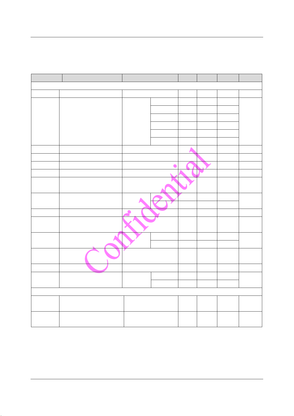
4 Electrical Characteristics
Table 4-1 DC Electrical Specification (Recommended O peration Conditions):
SYMBOL DESCRIPTION MIN TYP MAX UNIT
VDD
T
amb
V
IL
V
IH
V
TH
Table 4-2 DC Electrical Specification (Absolut e Maximum Ratings) :
SYMBOL DESCRIPTION MIN TYP MAX UNIT
T
amb
I
IN
V
IN
V
lna
Notes:
1. For Pin: SCLK, SDIO
Supply Voltage 2.7 3.0 3.3 V
Ambient Temperature
CMOS Low Level Input Voltage
CMOS High Level Input Voltage
CMOS Threshold Voltage
Ambient Temperature
Input Current
Input Voltage
(1)
(1)
VDD+0.3 V
LNA FM Input Level
-20 27 +75 ℃
0 0.3*VDD V
0.7*VDD VDD V
0.5*VDD V
-40 +90 °C
-10
+10 mA
-0.3
+10 dBm
Table 4-3 Power Consumption Specification
(VDD = 3.0V, TA = 25℃, unless otherwise specified)
SYMBOL DESCRIPTION CONDITION TYP UNIT
I
VDD
I
VDD
I
PD
Supply Current
Supply Current
Powerdown Current
Notes:
1. For strong input signal condition
2. For weak input signal condition
(1)
(2)
ENABLE=1
ENABLE=1
20 mA
21 mA
ENABLE=0 25
µA
The information contained herein is the exclusive property of RDA an d shall no t be di stributed, reproduced, or disclosed in whole or in
part without prior written permission of RDA.
Page 6 of 23
RDA Microelectronics, Inc. RDA5807NP FM Tuner V1.2
Input Common
5 Receiver Characteristics
Table 5-1 Receiv er Characteristics
(VDD = 3 V, TA = 25 °C, unless otherwise specified)
SYMBOL PARAMETER CONDITIONS MIN TYP MAX UNIT
General specifications
F
in
V Sensitivity
rf
IP3
in
α
am
S
200
S
400
FM Input Frequency Range
1,2,3
Input IP3
AM Suppression
4
80 - -
1,2
Adjacent Channel Selectivity
400KHz Selectivity
Audio L/R Output Voltage
V
; V
AFR
(Pins LOUT and ROUT)
AFL
Maximum Signal to Noise
S/N
α
SCS
Stereo Channel Separation
Ratio
1,2,3,5
Audio Output Loading
R
L
Resistance
Audio Total Harmonic
THD
Distortion
1,3,6
Audio Output L/R
α
AOI
R
BW
mute
audio
Imbalance
Mute Attenuation Ratio
Audio Response
1,6
1
1
Pins FMIN, LOUT, ROUT
Pins FMIN
V
com_rfin
Mode Voltage
Audio Output Common Mode
V
com
Notes:1. F
=65 to 115MHz; F
in
2. ∆f=22.5KHz; 3. B
5. P
=60dBUV; 6. ∆f=75KHz,fpilot=10% 7. Measured at V
RF
8. At LOUT and ROUT pins 9. Adjustable
Voltage
=1KHz; de-emphasis=75µs; MONO=1; L=R unless noted otherwise;
mod
AF
8
= 300Hz to 15KHz, RBW <=10Hz; 4. |f2-f1|>1MHz, f0=2xf1-f2, AGC disable, F
Adjust BAND Register 50 115 MHz
50MHz - 1.4 1.8
65MHz - 1.2 1.5
88MHz - 1.2 1.5
S/N=26dB
98MHz - 1.3 1.5
108MHz - 1.3 1.5
115MHz - 1.3 1.8
AGCD=1
m=0.3
60 - - dB
±200KHz 50 70 - dB
±400KHz 60 85 - dB
1,2
Volume [3:0] =1111 - 360 - mV
2
6
Stereo 53
Mono 55
57 55 -
35 - - dB
Single-ended 32 - - Ω
Volume[3:0]
=1111
R
load
R
load
Volume[3:0]=0000
1KHz=0dB
±3dB point
Low Freq High Freq - 14 -
- =1KΩ
0.15 0.2
- =32Ω 0.2 -
- - 0.05 dB
60 - - dB
9
100 -
0
1.0 1.05 1.1 V
=76 to 108MHz;
= 1 m V, f
EMF
RF
in
= 65 to 108MHz
µV EMF
dBµV
dB
%
Hz
V
The information contained herein is the exclusive property of RDA an d shall no t be di stributed, reproduced, or disclosed in whole or in
part without prior written permission of RDA.
Page 7 of 23

RDA Microelectronics, Inc. RDA5807NP FM Tuner V1.2
SCLK
SDIO
1-7 8 9 1-7 8
9
1-7 8 9
START
ACK
data high byteACKr/waddress
data low byte ACK STOP
t
su:sta
t
hd:sta
t
sp
START
t
su:sto
t
buf
t
su:datthd:dat
SCLK
SDIO
1-7 8 9
1-7 8
9
1-7 8 9
START
ACK
data high byteACKr/waddress
data low byte NACK STOP
t
sp
START
t
buf
t
su:sta
t
hd:sta
t
su:datthd:dat
t
su:sto
6 Serial Interface
2
6.1 I
C Interface Timing
Table 6-1 I
(VDD = 3.0 V, T
2
C Interface Timing Characteristics
= 25°C, unless otherwise specified)
A
PARAMETER SYMBOL TEST CONDITION MIN TYP MAX UNIT
SCLK Frequency
SCLK High Time
SCLK Low Time
Setup Time for START Condition
Hold Time for START Condition
Setup Time for STOP Condition
SDIO Input to SCLK↑ Setup t
SDIO Input to SCLK↓ Hold t
STOP to START Time
SDIO Output Fall Time
SDIO Input, SCLK Rise/Fall Time
Input Spike Suppression
SCLK, SDIO Capacitive Loading
Digital Input Pin Capacitance
t
f
t
t
t
su:sta
t
hd:sta
t
su:sto
su:dat
hd:dat
t
t
r:in /
t
C
scl
high
low
buf
f:out
sp
t
f:in
b
0 - 400 KHz
0.6 - -
1.3 - -
0.6 - -
0.6 - -
0.6 - -
100 - - ns
0 - 900 ns
1.3 - 20+0.1C 20+0.1C -
250 ns
b
300 ns
b
- - 50 ns
- - 50 pF
µs
µs
µs
µs
µs
µs
5 pF
Figure 6-1. I
2
C Interface Write Timing Diagram
Figure 6-2. I
The information contained herein is the exclusive property of RDA an d shall no t be di stributed, reproduced, or disclosed in whole or in
part without prior written permission of RDA.
2
C Interface Read Timing Diagram
Page 8 of 23

RDA Microelectronics, Inc. RDA5807NP FM Tuner V1.2
0 = Disabled; 1 = Bass boost enabled
℃ temperature. Only
0 = Seek down; 1 = Seek up
n the direction specified by
7 Register Definition
REG BITS NAME FUNCTION DEFAULT
00H 15:8 CHIPID[7:0]
02H 15 DHIZ
14 DMUTE
13 MONO
12 BASS
Chip ID.
Audio Output High-Z Disable.
0 = High impedance; 1 = Normal operation
Mute Disable.
0 = Mute; 1 = Normal operation
Mono Select.
0 = Stereo; 1 = Force mono
Bass Boost.
0x58
0
0
0
0
11 RCLK NON-CALIBRATE
MODE
0=RCLK clock is always supply
1=RCLK clock is not always supply when FM
work ( when 1, RDA5807FP can’t directly
support -20℃~70
suppory ±20℃ temperature swing from tune
point)
10 RCLK DIRECT INPUT MODE
9 SEEKUP
8 SEEK
7 SKMODE Seek Mode
6:4 CLK_MODE[2:0] 000=32.768kHz
3 RDS_EN RDS/RBDS enable
2 NEW_METHOD New Demodulate Method Enable, can improve
1 SOFT_RESET Soft reset.
1=RCLK clock use the directly input mode
Seek Up.
Seek.
0 = Disable stop seek; 1 = Enable
Seek begins i
SEEKUP and ends when a channel is found,
or the entire band has been searched.
The SEEK bit is set low and the STC bit is set
high when the seek operation completes.
0 = wrap at the upper or lower band limit and
continue seeking
1 = stop seeking at the upper or lower band
limit
001=12Mhz
101=24Mhz
010=13Mhz
110=26Mhz
011=19.2Mhz
111=38.4Mhz
If 1, rds/rbds enable
the receive sensitivity about 1dB.
If 0, not reset;
If 1, reset.
0
0
0
0
0
000
0
0
0
The information contained herein is the exclusive property of RDA an d shall no t be di stributed, reproduced, or disclosed in whole or in
part without prior written permission of RDA.
Page 9 of 23

RDA Microelectronics, Inc. RDA5807NP FM Tuner V1.2
is set high. The STC bit is set high when the
the tune operation completes..
REG BITS NAME FUNCTION DEFAULT
0 ENABLE
03H 15:6 CHAN[9:0]
5 DIRECT MODE
4 TUNE Tune
Power Up Enable.
0 = Disabled; 1 = Enabled
Channel Select.
BAND = 0
Frequency =
Channel Spacing (kHz) x CHAN+ 87.0 MHz
BAND = 1or 2
Frequency =
Channel Spacing (kHz) x CHAN + 76.0 MHz
BAND = 3
Frequency =
Channel Spacing (kHz) x CHAN + 65.0 MHz
CHAN is updated after a seek operation.
Directly Control Mode, Only used when test.
0 = Disable
1 = Enable
The tune operation begins when the TUNE bit
0
0x00
0
0
tune operation completes.
The tune bit is reset to low automatically when
3:2 BAND[1:0] Band Select.
00 = 87–108 MHz (US/Europe)
01 = 76–91 MHz (Japan)
10 = 76–108 MHz (world wide)
1
11
= 65 –76 MHz (East Europe) or 50-65MHz
1:0 SPACE[1:0] Channel Spacing .
00 = 100 kHz
01 = 200 kHz
10 = 50kHz
11 = 25KHz
04H 15 RSVD Reserved
14 STCIEN Seek/Tune Complete Interrupt Enable.
0 = Disable Interrupt
1 = Enable Interrupt
Setting STCIEN = 1 will generate a lo w pu lse on
GPIO2 when the interrupt occurs.
13:12 RSVD Reserved
11 DE
10 RSVD
9 SOFTMUTE_EN If 1, softmute enable
8 AFCD AFC disable.
De-emphasis.
0 = 75 µs; 1 = 50 µs
Reserved
If 0, afc work;
00
00
0
0
00
0
1
0
1
If 0x07h_bit<9> ( band )=1, 65-76MHz; =0, 50-76MHz
The information contained herein is the exclusive property of RDA an d shall no t be di stributed, reproduced, or disclosed in whole or in
part without prior written permission of RDA.
Page 10 of 23

RDA Microelectronics, Inc. RDA5807NP FM Tuner V1.2
If 1, enabled.
11 = High
10: FMIN
tput mute and output
11=open behind registers writing function
If 1, ws=0 ->l, ws=1 ->r.
REG BITS NAME FUNCTION DEFAULT
If 1, afc disabled.
7 RSVD Reserved
6 I2S_ENABLED I2S bus enable
If 0, disabled;
0
5:4 GPIO3[1:0]
3:2 GPIO2[1:0]
1:0 GPIO1[1:0]
05H 15 INT _MODE If 0, generate 5ms interrupt;
14:12 RSVD Reserved
11:8 SEEKTH[3:0]
7:6 LNA_PORT_SEL[1:0] LNA input port selection bit:
2
General Purpose I/O 3.
00 = High impedance
01 = Mono/Stereo indicator (ST)
10 = Low
11 = High
General Purpose I/O 2.
00 = High impedance
01 = Interrupt (INT)
10 = Low
General Purpose I/O 1.
00 = High impedance
01 = Reserved
10 = Low
11 = High
If 1, interrupt last until read reg0CH action
occurs.
Seek SNR threshold value
00
00
00
1
000
1000
10
5:4 RSVD
3:0 VOLUME[3:0]
06H 15 RSVD
14:13 OPEN_MODE[1:0]
12 I2S_MODE
11 SW_LR Ws relation to l/r channel.
10 SCLK_I_EDGE When I2S enable
2
This value is SNR threshold for seeking, and the default value 1000 is about 32dB SNR.
3 This function is open when I2S_Enabled=1.
The information contained herein is the exclusive property of RDA an d shall no t be di stributed, reproduced, or disclosed in whole or in
part without prior written permission of RDA.
3
3
3
Page 11 of 23
Resvered
DAC Gain Control Bits (V olume).
0000=min; 1111=max
Volume scale is logarithmic
When 0000, ou
impedance is very large
reserved
Open reserved register mode.
others: only open behind registers reading
function
If 0, master mode;
If 1, slave mode.
If 0, ws=0 ->r, ws=1 ->l;
If 0, use normal sclk internally;
00
1111
0
00
0
10
0

RDA Microelectronics, Inc. RDA5807NP FM Tuner V1.2
4'b1000: WS_STEP_48;
The seek fail flag is set when the seek
level greater than SEEKTH[5:0].
REG BITS NAME FUNCTION DEFAULT
If 1, inverte sclk internally.
9 DATA_SIGNED If 0, I2S output unsigned 16-bit audio data.
8 WS_I_EDGE If 0, use normal ws internally;
7:4 I2S_SW_CNT[4:0]
Only valid
in master mode
3 SW_O_EDGE If 1, invert ws output when as master.
2 SCLK_O_EDGE If 1 , invert sclk output when as master.
1 L_DELY If 1, L channel data delay 1T.
0 R_DELY If 1, R channel data delay 1T.
07H 15 RSVD Reserved 0
14:10 TH_SOFRBLEND[5:0] Threshold for noise soft blend setting, unit 2 dB 10000
9 65M_50M MODE V a lid when band[1:0] = 2’b11 (0x03H_bit<3:2>)
8 RSVD Reserved 0
7:2 SEEK_TH_OLD
1 SOFTBLEND_EN If 1, Softblend enable 1
0 FREQ_MODE If 1, then freq setting changed.
0AH 15 RDSR RDS ready
14 STC Seek/Tune Complete.
13 SF
3
0
If 1, I2S output signed 16-bit audio data.
3
0
If 1, inverte ws internally.
3
4'b0111: WS_STEP=44.1kbps;
0000
4'b0110: WS_STEP=32kbps;
4'b0101: WS_STEP=24kbps;
4'b0100: WS_STEP=22.05kbps;
4'b0011: WS_STEP=16kbps;
4'b0010: WS_STEP=12kbps;
4'b0001: WS_STEP=11.025kbps;
4'b0000: WS_STEP=8kbps;
3
3
3
3
0
0
0
0
1
1 = 65~76 MHz;
0 = 50~76 MHz.
4
000000
Seek threshold for old seek mode, Valid when
Seek_Mode=001
0
Freq = 76000(or 87000) kHz + freq_direct (08H)
kHz.
0
0 = No RDS/RBDS group ready(default)
1 = New RDS/RBDS group ready
0
0 = Not complete
1 = Complete
The seek/tune complete flag is set when the
seek or tune operation completes.
Seek Fail.
0 = Seek successful; 1 = Seek failure
0
12 RDSS RDS S ynchronization
4
0x20H_bit<14:12>, Seek_Mode register. Default value is 000; When = 001, will add the 5807SP seek mode.
The information contained herein is the exclusive property of RDA an d shall no t be di stributed, reproduced, or disclosed in whole or in
part without prior written permission of RDA.
operation fails to find a channel with an RSSI
0
0 = RDS decoder not synchronized(default)
Page 12 of 23

RDA Microelectronics, Inc. RDA5807NP FM Tuner V1.2
0 = no Block E has been found
Frequency = Channel Spacing (kHz) x
Frequency = Channel Spacing (kHz) x
g (kHz) x
seek operation.
Block Errors Level of RDS_DATA_0, and is
Block Errors Level of RDS_DATA_1, and is
(in RDS mode ) or E (in RBDS mode when
REG BITS NAME FUNCTION DEFAULT
1 = RDS decoder synchronized
Available only in RDS Verbose mode
11 BLK_E When RDS enable:
1 = Block E has been found
0
10 ST
9:0 READCHAN[9:0] Read Chann el.
0BH 15:9 RSSI[6:0] RSSI.
8 FM TRUE 1 = th e current ch annel is a station
7 FM_READY 1=ready
<6:5> reserved
<4> ABCD_E 1= the block id of register 0cH,0dH,0eH,0fH is E
<3:2> BLERA[1:0]
<1:0> BLERB[1:0]
Stereo Indicator.
0 = Mono; 1 = Stereo
Stereo indication is available on GPIO3 by
setting GPIO3[1:0] =01.
BAND = 0
READCHAN[9:0]+ 87.0 MHz
BAND = 1 or 2
READCHAN[9:0]+ 76.0 MHz
BAND = 3
Frequency = Channel Spacin
READCHAN[9:0]+ 65.0 MHz
READCHAN[9:0] is updated after a tune or
000000 = min
111111 = max
RSSI scale is logarithmic.
0 = the current channel is not a station
0=not ready
0= the block id of register 0cH, 0dH, 0eH,0fH is
A, B, C, D
always read as Errors Level of RDS BLOCK A
(in RDS mode) or BLOCK E (in RBDS mode
when ABCD_E flag is 1)
00= 0 errors requiring correction
01= 1~2 errors requiring correction
10= 3~5 errors requiring correction
11= 6+ errors or error in checkword, correction
not possible.
Available only in RDS Verbose mode
always read as Errors Level of RDS BLOCK B
1
8’h00
0
0
0
0
The information contained herein is the exclusive property of RDA an d shall no t be di stributed, reproduced, or disclosed in whole or in
part without prior written permission of RDA.
Page 13 of 23

RDA Microelectronics, Inc. RDA5807NP FM Tuner V1.2
BLOCK A ( in RDS mode) or BLOCK E (in
BLOCK B ( in RDS mode) or BLOCK E (in
BLOCK C ( in RDS mode) or BLOCK E (in
de) or BLOCK E (in
REG BITS NAME FUNCTION DEFAULT
ABCD_E flag is 1).
00= 0 errors requiring correction
01= 1~2 errors requiring correction
10= 3~5 errors requiring correction
11= 6+ errors or error in checkword, correction
not possible.
Available only in RDS Verbose mode
0CH <15:0> RDSA[15:0]
RBDS mode when ABCD_E flag is 1)
0DH <15:0> RDSB[15:0]
RBDS mode when ABCD_E flag is 1)
0EH <15:0> RDSC[15:0]
RBDS mode when ABCD_E flag is 1)
0FH <15:0> RDSD[15:0] BLOCK D ( in RDS mo
RBDS mode when ABCD_E flag is 1)
16’h5803
16’h5804
16’h5808
16’h5804
The information contained herein is the exclusive property of RDA an d shall no t be di stributed, reproduced, or disclosed in whole or in
part without prior written permission of RDA.
Page 14 of 23

RDA Microelectronics, Inc. RDA5807NP FM Tuner V1.2
RDS5807FP
SOP16
1
2
3
4
5
6
7
8
16
15
14
13
12
11
10
9
GPIO2
GPIO3
GND
ROUT
LOUT
RCLK
VDD
GND
GPIO1
GND
RF GND
FMIN
GND
GND
SCLK
SDA
8 Pins Description
Figure 8-1. RDA5807FP Top View
Table 8-1 RDA5807FP SOP16 Pins Description
SYMBOL PIN DESCRIPTION
GND 2, 5,6,11,14 Ground. Connect to ground plane on PCB
RF GND 3 RF Ground. Connect to RF ground plane to PCB
FMIN 4 FM single input
RCLK 9 32.768KHz reference clock input
VDD 10 Power supply
LOUT,ROUT 13,12 Right/Left audio output
SCLK 7 Clock input for serial control bus
SDA 8 Data input/output for serial control bus
GPIO1,GPIO2,GPIO3 1,16,15 General purpose input/output
The information contained herein is the exclusive property of RDA an d shall no t be di stributed, reproduced, or disclosed in whole or in
part without prior written permission of RDA.
Page 15 of 23

RDA Microelectronics, Inc. RDA5807NP FM Tuner V1.2
FMIN
FMs
MN1
Rload
50pF
RCLK
5M
20pF
6pF
INV
5M
0x02h_bit<10>
VDD
=1
=0
47K
S
in
S
out
MN1
SDIO\SCLK
GPIO1\2\3
in
Out
200K
VDD
Table 8-2 Interna l Pin C onfig ur ati on
SYMBOL PIN DESCRIPTION
FMIN 4
RCLK 9
SCLK/SDIO 7/8
GPIO1/GPIO2/GPIO3
1/16/15
The information contained herein is the exclusive property of RDA an d shall no t be di stributed, reproduced, or disclosed in whole or in
part without prior written permission of RDA.
Page 16 of 23

RDA Microelectronics, Inc. RDA5807NP FM Tuner V1.2
RDA5807FP
SOP16
GPIO1
GND
RF GND
FMIN
GND
GND
SCLK
SDA
GPIO2
GPIO3
GND
ROUT
LOUT
RCLK
VDD
GND
J1
C3 4.7uF
C4 4.7uF
32.768kHz
L1 100nH
C2 24pF
V1
C1
22nF
SCLK
SDA
F1 1.5K@100MHz
F2 1.5K@100MHz
U1
C7 100pF
ESD
9 Application Diagram
9.1 RDA5807FP Common Application :
Notes:
1. J1: Common 32Ω Resistance
Headphone;
2. V1: Power Supply (2.7~3.3V);
3. FM Choke (L1 and C2) for Audio
Common and LNA Input Common;
4. Place C1 Close to 5807NP pin10.
Figure 9-1. RDA5807FP FM Tuner Application Diagram (TCXO Application)
9.1.1 Bill of Materials:
COMPONENT VALUE DESCRIPTION SUPPLIER
U1 RDA5807FP
SOP16
J1 Common 32Ω Resistance Headphone
L1/C2 100nH/24pF LC Chock for FMIN Input Murata
C4,C5 125µF Audio AC Couple Capacitors Murata
Broadcast FM Radio Tuner RDA
C1 22nF Power Supply Bypass Capacitor Murata
C7 100pF AC Couple Capacitors Murata
ESD TVS
F1/F2 1.5K@100MHz FM Band Ferrite Murata
The information contained herein is the exclusive property of RDA an d shall no t be di stributed, reproduced, or disclosed in whole or in
part without prior written permission of RDA.
Page 17 of 23

RDA Microelectronics, Inc. RDA5807NP FM Tuner V1.2
10 Physical Dimension
Figure 10-1 illustrates the package details for the RDA5807FP. The package is lead-free and
RoHS-compliant.
The information contained herein is the exclusive property of RDA an d shall no t be di stributed, reproduced, or disclosed in whole or in
part without prior written permission of RDA.
Page 18 of 23

RDA Microelectronics, Inc. RDA5807NP FM Tuner V1.2
Figure 10-1. 16 PIN SOP PCB Land Patt er n
11 PCB Land Pattern:
Profile Feature Sn-Pb Eutectic Assembly Pb-Free Assembly
Average Ramp-Up Rate
to T
(T
Smax
Preheat
-Temperature Min (T
-Temperature Max (T
-Time (t
smin
to t
Time maintained above:
-Temperature (T
-Time (t
L
)
p
)
smax
L
Figure 11.Classification Reflow Profile
o
3
o
smin
smax
)
)
)
100
C
o
C
100
60-120 seconds
)
183
o
C
60-150seconds
o
3 C/second max.
C/second max.
o
150
C
o
C
200
60-180 seconds
o
217
C
60-150 seconds
Peak /Classification
Temperature(T
)
p
Time within 5 oC of actual
Peak Temperature (t
)
p
Ramp-Down Rate 6
Time 25
The information contained herein is the exclusive property of RDA an d shall no t be di stributed, reproduced, or disclosed in whole or in
part without prior written permission of RDA.
o
C to Peak
Page 19 of 23
See Table-II
10-30 seconds
o
6 minutes max.
See Table-III
20-40 seconds
o
6 C/second max.
C/seconds max.
8 minutes max.

RDA Microelectronics, Inc. RDA5807NP FM Tuner V1.2
Temperature
≥
<
≥
<
>
≥
Table-I Classification Reflow Profiles
Package Thickness Volume mm
<350
2.5mm 240 + 0/-5
2.5mm 225 + 0/-5
o
o
3
Volume mm
350
225 + 0/-5 C
225 + 0/-5 C
3
o
C
o
C
Table – II SnPb Eutectic Process – Package Peak Reflow Temperatures
Package
Thickness
Volume mm
350
<1.6mm 260 + 0
1.6mm – 2.5mm 260 + 0
2.5mm 250 + 0
3
Volume mm
350-2000
o
o
o
260 + 0 C *
250 + 0 C *
245 + 0 C *
3
Volume mm
2000
o
o
o
260 + 0 C *
245 + 0 C *
245 + 0 C *
o
o
o
C *
C *
C *
*Tolerance : The device manufacturer/supplier shall assure process compatibility up to and
including the stated classification temperature(this mean Peak reflow temperature + 0
example 260+ 0
o
C ) at the rated MSL Level.
o
Table – III Pb-free Process – Package Classification Reflow Temperatures
3
C. For
Note 1: All temperature refer topside of the package. Measured on the package body surface.
Note 2: The profiling tolerance is + 0
o
C, - X
o
C (based on machine variation
capability)whatever
is required to control the profile process but at no time will it exceed - 5
o
C. The
producer assures process compatibility at the peak reflow profile temperatures defined
in Table –III.
Note 3: Package volume excludes external terminals(balls, bumps, lands, leads) and/or non
integral heat sinks.
Note 4: The maximum component temperature reached during reflow depends on package the
thickness and volume. The use of convection reflow processes reduces the thermal
gradients between packages. However, thermal gradients due to differences in
thermal mass of SMD package may sill exist.
Note 5: Components intended for use in a “lead-free” assembly process shall be evaluated
using the “lead free” classification temperatures and profiles defined in Table-I II III
whether or not lead free.
The information contained herein is the exclusive property of RDA an d shall no t be di stributed, reproduced, or disclosed in whole or in
part without prior written permission of RDA.
Page 20 of 23

RDA Microelectronics, Inc. RDA5807NP FM Tuner V1.2
RoHS Compliant
The product does not contain lead, mercury, cadmium, hexavalent chromium, polybrominated biphenyls (PBB)
or polybrominated diphenyl ethers (PBDE), and are therefore considered RoHS com pli ant.
ESD Sensitivity
Integrated circuits are ESD sensitive and can be damaged by static electricity. Proper ESD
techniques should be used when handling these devices.
The information contained herein is the exclusive property of RDA an d shall no t be di stributed, reproduced, or disclosed in whole or in
part without prior written permission of RDA.
Page 21 of 23

RDA Microelectronics, Inc. RDA5807NP FM Tuner V1.2
12 Change List
REV DATE AUTHER CHANGE DESCRIPTION
V1.0 2011-07-18 Chun Zhao, Yanan Liu Original Draft.
The information contained herein is the exclusive property of RDA an d shall no t be di stributed, reproduced, or disclosed in whole or in
part without prior written permission of RDA.
Page 22 of 23

RDA Microelectronics, Inc. RDA5807NP FM Tuner V1.2
Contact Information
RDA Microelectronics (Shanghai), Inc.
Suite 1108 Block A , e-Wing Center, 113 Zhichun Road Haidian District, Beijing
Tel: 86-10-62635360
Fax: 86-10-82612663
Postal Code: 100086
Suite 302 Building 2, 690 Bibo Road Pudong District, Shanghai
Tel: 86-21-50271108
Fax: 86-21-50271099
Postal Code: 201203
Copyright © RDA Microelectronics Inc. 2006. All rights are reserved.
Reproduction in whole or in part is prohibited without the prior written consent of the copyright owner.
The information contained herein is the exclusive property of RDA an d shall no t be di stributed, reproduced, or disclosed in whole or in
part without prior written permission of RDA.
Page 23 of 23
 Loading...