
RS2640
SPECIFICATIONS (Subject to change without notice)
Line Voltage: 120vAC +/- 10% @ 60Hz
AMPLIFIER:
Power Bandwidth: 60-20,000 Hz
Frequency Response:
Main Channels: 60-16,000 Hz +0/-3dB
Hum, at Min Volume (unweighted): 1m Vrms @ 6 ohms
Muting Attenuation: 70 db
Signal to Noise:
Weighted: 65 db
Crosstalk: 50 db
Maximum Input: 2 Vrms
Power Output: 80W @ 10% THD
Headphone Output: 6 mW
AM RADIO PERFORMANCE
Tuning Range: 530-1710
Usable Sensitivity @ 20dB S/N: 600 uV/m
S/N: 40 db
Auto Stop Sensitivity @ 1kHz: 1000 mV/m
FM RADIO PERFORMANCE
Tuning Range: 87.5 – 107.9Mhz
Minimum Sensitivity: 26 dbf
Frequency Response: 100 – 10 KHz +/- 5 db
Stereo Separation @ 1kHz: 20 db
S/N Ratio stereo A-weighted: 55 dbf
Auto Stop Sensitivity @ 99MHz: 32 dbf
TAPE
Frequency Response: 63 – 8 kHz +/-5 db
S/N Ratio (Playback): 45 db
Channel Separation @1 kHz: 34 db
Wow & Flutter: 0.2%
CD
Frequency Response: 60 – 20,000 Hz +0/-3 db
S/N Ratio: 75 db
Eccentricity: 140 um
Vertical deviation: 780 mm
Page 1-3
RS2640 RS2640
DISASSEMBLY DISASSEMBLY
Cover Removal
Note: Perform all disassembly procedures in the order
presented. When reassembling, use the reverse
procedure. Make sure that all leads/wiring are
routed correctly when reassembling.
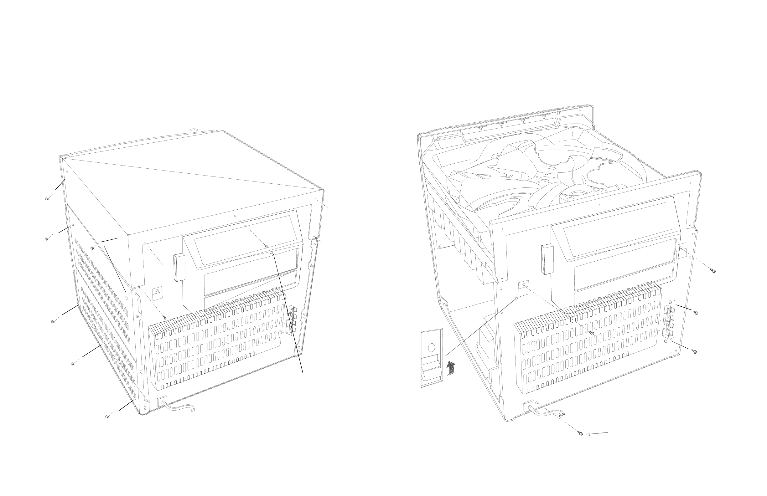
1. Remove the screw located on the backside of the unit as
shown in Figure 1. Remove seven (7) screws located on
the left and right side of the cover
2. Remove top panel by lifting upward from rear and
separating tabs from backside of front plate.
Back Panel Removal
1. Remove cover.
2. Remove thirteen (13) screws from the back of unit as
shown in Figure 2.
3. Lift CD tray to release tabs on back panel as shown in
Figure 2.
Fig. 1 Cover Removal
1/2 PAN HEAD SCREW
1 OF 5
Remove screws
Located on the Back of Unit.
Fig. 2 Back Panel Removal
Page 2-2Page 2-1
RS2640 RS2640
DISASSEMBLY DISASSEMBLY
CD Mechanism Removal
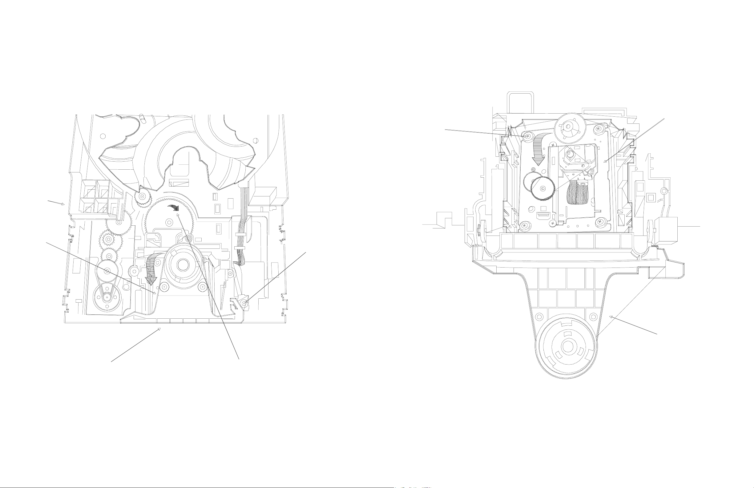
1. Plug unit in and extend the CD tray. While extended unplug the unit.
2. Remove top cover.
3. Remove side panels.
4. Remove the back panel
5. Remove one (1) screw from the CD Arm Stop as shown
in Figure 3.
CD Mechanism Removal (Cont’d)
7. Remove four (4) srews fron CD Mechanism Assembly
as shown in Figure 4.
8. Release one (1) wire from catch on bottom of CD Tray.
9. Release CD Mechanism Assembly from mount by pulling towards the rear and lifting gently.
Remove (4) screws
CD Tray
CD Mechanism Assembly
CD Arm
Rear of Unit
Remove (1) screw
CD Arm
Rotate Gear Clockwise
Fig. 3 CD Mechanism Removal
Fig. 4 CD Mechanism Removal
Page 2-3
Page 2-4

RS2640 RS2640
DISASSEMBLY DISASSEMBLY
CD Mechanism Removal (Cont’d)
10. Disconnect one (1) Ribon wire from CD Mechanism
Assembly as shown in Figure 5.
Risconnect Wire from
CD Mechanism Assembly
Fig. 5 CD Mechanism Removal
Page 2-5
Page 2-6

RS2640 RS2640
ALIGNMENT PROCEDURES
Operating Conditions
Unless otherwise noted, the following conditions must be
observed when aligning the RS2640:
1. Chassis must be operated from a 120VAC isolation
transformer, with line voltage set to 120VAC (±2.0V).
2. Set controls (Volume, Tone, Balance, etc.) to mid-range.
3. Procedures must be performed in the sequence given.
4. A 10X probe must be used for oscilloscope and frequency measurements.
5. Minimum warm-up time is 10 minutes
Required Test Equipment
Personal Computer: IBM or Compatible 486DX 66 meg
PC (or LAPTOP) with 16 MEG Memory, VGA Monitor, one
3 1/2” floppy drive, 540 Meg or larger hard drive, compatible mouse, one parallel port dedicated for service interface
box and one port for mouse, Windows 95, 4X CD ROM,
Printer and Sound Card.
Isolation Transformer:
Digital Voltmeter: Range .1V DC to 1000V DC, Accuracy: ±
.5%/
True “RMS” Voltmeter: Range: 01 to 1000 Volts ± .5% Ac-
curacy
DC Voltage Supply: Range: 0 to 50V, 2A—Well Filtered
Temperature Controlled Soldering Station: Grounded Tip
Type—Tip Temperature 500F to 800F Adjustable
Frequency Counter: Range: 50Hz to 100 MHz Sensitivity:
25mV to 5V. Equipped with Lo-Cap Probe (10:1 Attenuation)
AC Variac: Continuously Variable. Isolation Type Preferred
NTSC Video Signal Generator: Must provide 1V P-P Nega-
tive Sync, Video into 75-OHM input. Produce, standard NTSC
75% Saturated Color Bars with 100% White Window. (B&K
1249, or equivalent)
RF Signal Generator: 100 kHz to 150 MHz .1V RMS, Int.
Mod. 1KHz 30%
TAG001 Tuner Alignment Generator (stock # 215568) or
equivalent: Equivalent Generator must have RF output capa-
bilities for cable channels 1-125.
Cross Hatch Generator: Must have RF output.
S-Video Source: Must provide standard Y-C separated sig-
nal. SVHS output of VCR, DSS or DVD will suffice
Dual Trace, Delayed Sweep Oscilloscope: 25 MHz with
Channel invert capability. Sensitivity’ 5mV/cm Maximum
Sweep Rate: .1us/cm.
Hot Air Desoldering Station:
MTS TV Stereo Generator: Must produce L-R, L+R, SAP at
300 Hz, 1KHz, 8KHz(B&K 2009, or equivalent).
FM IF ALIGNMENT
Test Points:
Input: TP 001 TP001G (RFGND)
Output: TP 003 TP001G (AGND)
1. Connect an FM IF signal to TP004 (Pin 39 of UIC001)
and TP004G (IFGND) through a 1nF capacitor in series
with a 10K resistor.
2. Connect an Oscilloscope to the IF signal output at TP009
(Pin 10 of IC001) and TP009G (AGND) through a 4.7
uF capacitor.
3. Align TF006 to obtain a clear display on the oscilloscope
without any interference.
4. Ensure that the curve is not saturated.
5. Tune the set to 98.10 MHz
6. Apply an un-modulated mono RF signal at 98.10 MHz
with RF input level of 1 mV to TP001 and TP001G
(RFGND).
7. Connect a frequency counter to TP003 (Pin 33 of IC001)
thru a capacitor 0.1 uF
8. Check TP003 and align TF006 to get 10.7 MHz ± 10
KHz.
TUNER
SECTION
TP-004G
TP-009G
TP-004
TP-009
1 nF 10K
4.7uF
Figure 1.
IN
OUT
10.60
10.70
10.80
Figure 2.
ALIGNMENT PROCEDURES
FM OSCILLATOR AND RF ALIGNMENT
Test Points:
Input: TP001 TP001G (RFGND)
Output: TP007/TP008 TP009G (AGND)
Tuning(VT):TP002 TP009G (AGND)
1. Set frequency to 87.5 MHz.
Adjust FM Osc coil (L004) to obtain 1.0 to 1.05V at
TP002 (VT) and TP009G (AGND).
2. Set frequency to 108.10 MHz.
Adjust Vari-Cap (CV002) to obtain 7.0V ±0.5 at TP002
and TP009G (AGND).
3. Repeat steps 1 and 2 above until the band coverages falls
within the specified VT voltage.
4. Feed a FM RF signal to a matching balanced pad (50
ohm - 75 ohm) at TP 001 and TPR001G (RFGND).
5. Use the circuit in figure 3 to detect the signal from TP
007/008 and TP009G (AGND).
6. Set frequency to 90.10 MHz and adjust L003 until maximum amplitude is reached.
7. Set frequency to 106.10 MHz to see whether approximate amplitude is the same as in step 6.
8. Set frequency to 98.10 MHz and check for approximate
amplitude.
1.00V
DC Voltmeter
TUNER
TP-001G
TP-002
TP-001
TP-001G
TP-007/008
TP-009G
OSC ILLOSCOP E
4.7uF
FIGURE 3
IN OUT
FM STEREO ALIGNMENT
Test Points:
Input: TP001 TP001G (RFGND)
Output: TP005 TP010G (DGND)
TUNER SECTION
FM Signal Generator
TP-0 10
RV-001
TP-001
TP-001G
TP-006
TP- 005
FIGU RE 4
Frequenc y Counter
152.000kHz
98.10M Hz
1. Apply an un-modulated mono RF signal at 98.10 MHz
with RF input level of 1 mV to TP001 and TP001G
(RFGND).
2. Search to 98.10 MHz (Remove the VT probe during
search)
3. Connect a 10K from TP005 to TP010G (DGND).
4. Connect a frequency counter to TP005 (Pin 24 of IC001)
and TP010G (DGND), short TP010 (Pin 27 of IC001)
to TP010G (DGND, Pin 26 of IC001).
5. Check TP005 and align RV001 to get 152 KHz ± 1 KHz.
6. Apply a stereo 98.10 MHz signal to the set. Ensure the
Stereo indicator lights up. Signal strength must be less
than 32dB.
7. Remove the 10K resistor from TP005 and TP010G installed in step 3.
Page 3-2Page 3-1

RS2640 RS2640
ALIGNMENT PROCEDURES ALIGNMENT PROCEDURES
AM OSCILLATOR ALIGNMENT (MW)
Test Points:
Input: AM Antenna Loop TP001G (RFGND)
Output: TP007/TP008 TP009G (AGND)
Tuning(VT):TP002 TP009G (AGND)
1. Set frequency to 530 KHz .
2 Adjust MW Osc coil (TF003) to obtain 1.4 ± 0.05V at
TP 002 and TP009G.
3. Set frequency to 1710 KHz. Ensure the MW-VT at TP002
and TP009G is 8.0 ± 1 V
AM OSCILLATOR ALIGNMENT (LW)
Test Points:
Input: AM Antenna Loop TP001G (RFGND)
Output: TP007/TP008 TP009G (AGND)
Tuning(VT):TP002 TP009G (AGND)
1. Set frequency to 150 KHz.
2. Adjust MW Osc coil (TF003) to obtain 1.51 ±0.01V at
TP 002 and TP009G.
3. Set frequency to 283 KHz. Ensure the MW-VT at TP002
and TP009G is 4.6 ± 1V
AM IF AND AFC ALIGNMENT
Test Points:
Input: AM Antenna Loop TP001G (RFGND)
Output: TP011 TP004G (IFGND)
1. Connect an AM IF signal to AM OSC, TP012 (pin 6 of
IC001) and TP001G (RPGND).
2. Detect the output signal at TP009 (pin 10 of IC001) and
TP009G (AGND) as shown below in figure 5.
3. Adjust TF005 & TF008 until maximum amplitude is
reached
4. Send an un-modulated RF signal at 1000 KHz with RF
level of 100mV.
5. Tune the receiver to search up/down (remove the VT
probe during search). It will stop after acquiring this
signal.
6. Connect a frequency counter to TP011 (pin 36 of IC001)
and TP004G (IFGND) thru a capacitor 1uF
7. Check TP011 (pin 36 of IC001) and align TF007 to get
450 KHz ± 1 KHz.
AM RF ALIGNMENT (MW)
Test Points:
Input: AM Antenna Loop TP001G (RFGND)
Output: TP007/TP008 TP009G (AGND)
1. Apply a modulated (400 Hz) MW RF signal at 630 KHz
with low RF level of 300 uV.
2. Detect the signal from TP 007/008 and TP009G
(AGND). Adjust TF001 for the maximum amplitude.
AM RF ALIGNMENT (LW)
Test Points:
Input: AM Antenna Loop TP001G (RFGND)
Output: TP007/TP008 TP009G (AGND)
1. Apply a modulated (400 Hz) MW RF signal at 170 KHz
with low RF level of 300 uV.
2. Detect the signal from TP 007/008 and TP009G (AGND.
Adjust TF001 for the maximum amplitude.
MAIN BOARD TAPE ALIGNMENT
Alignment for the cassette portion should be done at the
semi - encased stage.
TUNER
TP012
TP004G
TP009
TP009G
445
AZIMUTH ALIGNMENT
1uF
4.7uF
FIGURE 5
IN
OUT
455
1. In tape transport 1, playback a test tape (TCC-153) freq.
10 KHz.
2. Connect the speaker outputs to a dual trace oscilloscope.
3. Adjust the azimuth screw at the tape head to obtain the
maximum amplitude on both channels. (Both channels
must be in phase).
TAPE SPEED ADJUSTMENT
1. Rewind the test tape (MTT-111 DN 3khz) until both the
spools on the left and right hubs are equal.
2. Connect the output to the WOW -FLUTTER METER.
3. Adjust the trimmer in the motor to obtain a playback
freq. of 3KHz ± 60 Hz.
RECORD BIAS OSCILLATOR ALIGNMENT
1. Place a tape inside the set. Ensure that the tape is not
450
record protected.
2. Select Tape mode and engage the Record button.
3. Monitor TP60 and TP60G (ground). Ensure that the
scope/meter does not have an activated low pass filter.
Adjust L302 & L303 to obtain a voltage of 12Vrms±5%.
Page 3-4Page 3-3
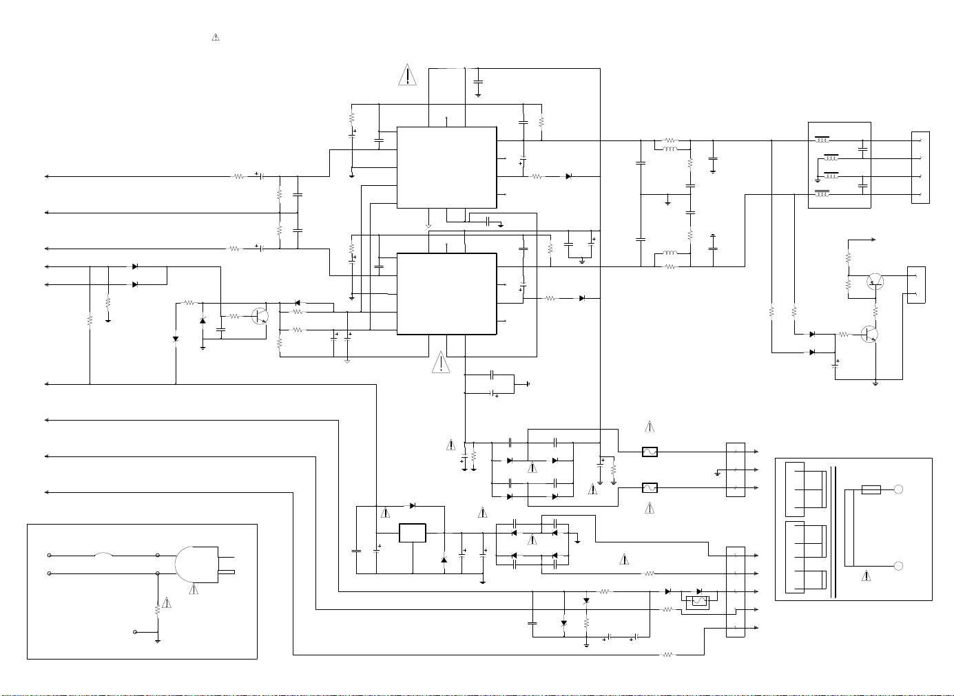
NOTES:
1. Unless otherwise specified:
A. All resistor values are in ohms
B. All Capacitor values are in uF
2. Voltages are positive with respect
to ground under no signal conditions
and volume control minimum
AUDIO_L
AGND
AUDIO_R
R512
6K8
1/16W
1N4148
1N4148
D515
D516
AMP_MUTE
H/P_IN
H/P_MUTE
1/16W
R511
10K
+10V
-30V
FIL+
FIL-
X883
X884
LIVE
JP881
NEUTRAL
R881
3M3
1/2W
X885
SHIELD_GND
On transformer BD
3. Replace transistors with type
specified from replacement parts list
4. * and indicates critical safety
components. Replace only with those
specified from replacement parts list
to maintain proper performances and
safety of this unit.
R502L
C502L
33K
1uF
1/16W
50V
R507L
100K
1/16W
R507R
100K
1/16W
C502R
R502R
1uF
33K
50V
1/16W
WARNING
SEE NOTE
R502
470
1/16W
D501
1/2W
2V4
D504
L
N
WARNING
SEE NOTE
R510
5V1
1K 1/16W
1/2W
100pF
C502
50V
L
N
KTC3875GR
Q501
1/16W
1N4148
D503
R525
33K
1/16W
R529
10K
1/16W
1K5
R532
C507L
470pF
50V
C507R
470pF
50V
10uF
C534
50V
R503L
1/16W
R503R
C509R
390
C509L
50V
1/16W
47uF
50V
4
AMPLIFIER\POWER SUPPLY SCHEMATIC
C518
100nF
111213
BOOT_LOADER
BUFFER_DRIVER
-VS
-PWVS +PWVS
8
111213
BOOT_LOADER
BUFFER_DRIVER
-VS
-PWVS +PWVS
8
-POWER_SUPPLY
C512
4700uF
50V
2200uF
C516
22uF
25V
AGND
BOOTSTRAP
CLIP_DET
15
BOOTSTRAP
CLIP_DET
15
100uF
50V
R530
1/2W
WARNING
SEE NOTE
C514
25V
63V
C501L
R501L
5pF
33k
50V
OUT
14
5 6
C524
100nF
63V
C501R
OUT
14
5 6
C520
100nF
1/16W
C537
22uF
25V
R505L
D501L
2K2
1N4148
1/16W
C533
1/16W
33k
R505R
2K2
1/16W
100nF
100uF
63V
50V
C539
D501R
1N4148
R501R
5pF
50V
C538
22uF
25V
63V
C505L
1NF
50V
C505R
1NF
50V
R510L
L501L
0.5uH
L501R
0.5uH
R510R
10
1/4W
C518L
10
1/4W
100nF
R512L
1/16W
16V
C518R
100nF
R512R
1/16W
C521L
330nF
50V
4R7
16V
4R7
C521R
330nF
50V
C540
+POWER_SUPPLY
C532
1N5402
D510
D512
100nF
50V
50V
C807
100nF
C526
100nF
100V
D506
C513
1N5402
4700uF
C528
WARNING
SEE NOTE
100nF
D508
WARNING
SEE NOTE
C531
50V
1N4001
1N4001
1.3W
D509
D511
27V
100V
1N5402
C530
100nF
50V
D820
100nF
50V
7.5V
1/2W
R885
50V
WARNING
SEE NOTE
220 1/2W
D819
10k
1/4W
R886 D821
C806
100uF
WARNING
SEE NOTE
F503
5S_5A_125V
US:
R531
4K7
1/2W
F504
5S_5A_125V
US:
WARNING
SEE NOTE
RF505
WARNING
1W
0.27
SEE NOTE
D822
1N4001
1N4001
R888
1 2
PF01
1
1/4W
C805
100uF
50V
50V
R889
1
1/4W
N/A
C525
100nF 100V
D505
4K7
1N5402
C527
100nF 100V
D507
C529
100nF
1N4001
1N4001
WARNING
SEE NOTE
7
IN-
+VS
C535
10uF
50V
C523
100nF
25V
C522L
1NF
50V
C522R
234
IN+
SGND
IC501
TDA7293
MUTE
STBY-GND
STBY
9 10
234
1NF
50V
9 10
WARNING
SEE NOTE
3
C515
22uF
16V
IN-
IN+
SGND
MUTE
STBY
OUT
D513
1N4148
IC503
KIA7812
GND
2
IN
1
7
+VS
IC502
TDA7293
STBY-GND
1
WARNING
SEE NOTE
1
D514
>25V
1/2W
WARNING
SEE NOTE
47uF
390
L502L
5uH
N801A
1 2 3
12345
N801B
JW3
JW2
JW1
JW04
JW05
JW06
JW07
JW08
R506L
22k
1/16W
1/16W
TO N801B TO N801A
2 3 4 51 321
L
L503L
R
L502R
5uH
R506R
22k
D502R
1N4148
D502L
1N4148
TRANSFORMER (EI76X50)
L503R
EU only
C519L
5uH
100nF 16V
5uH
C519R
100nF
R509
10
1/4W
R505
10K
1/16W
R503
10K
1/16W
KTC3875GR
Q503
C503
47uF
25V
FUSE INSIDE X`MER
WARNING
SEE NOTE
L OUTPUT
16V
R OUTPUT
+10V
KTA1273
Q502
R504
1K
1/4W
ON X'FORMER BD
FROM
BOARD
AC
NJ501
TO FAN
12
X883
X884
MAIN OUTPUT
1 2 3 4
N501
 Loading...