

Page 1
Communications Systems
RDR3600V
Service Manual
RCA Communications Systems
Page 2
Circuit Description
、 、 Frequencies constitute
一
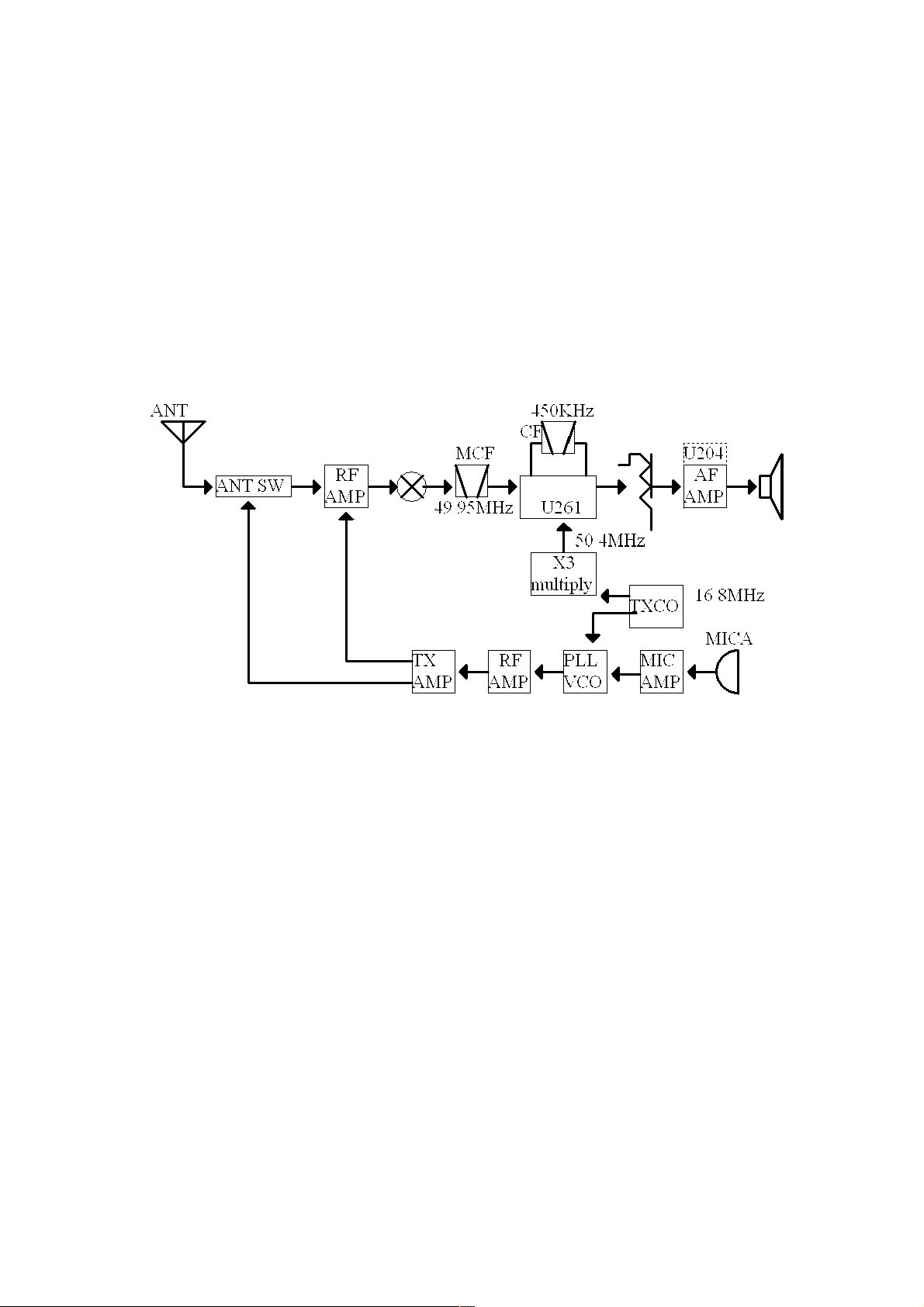
The receiver uses secondary frequency conversion. The first IF is 49.95 MHz and the second IF is
450 kHz. The first local oscillation signal is provided by the PLL circuit.
The PLL circuit generates the required transmit frequency
as picture 1 Frequency structu
、 Receiving department
二、
Frequency structure of receiving department as picture 2
re
Page 3
As picture 2 receiving department
1. The front-end (RF amplifier)
From the antenna signal into the transmit/receive switch diode circuits(D501,D503and D504)to
amplify.This signal passes through BPF (L508) and then enters mixing.These BPFs are adjusted by the
variable capacitors (D505, D506 and D512).The voltage of the input variable capacitor is adjusted by the
voltage output of the microprocessor (U301).
2. First
The signal of the front end is mixed with the first local oscillator signal generated by the PLL
circuit at Q1 to generate a firs
resulting signal is filtered by XF501
mixer
t intermediate frequency signal at a frequency of 49.95 MHz,and the
3. If amplifier circuit
The first intermediate frequency signal eliminates the signal of adjacent channel by crystal filter
(XF501) and amplifi
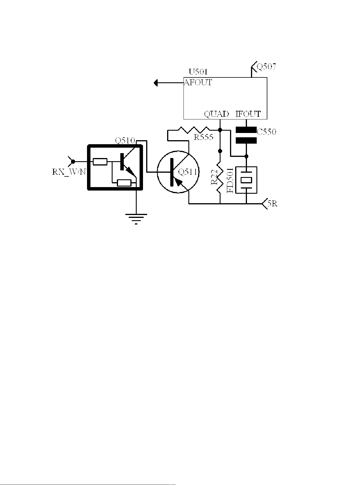
enters the intermediate frequency system chip (U501).The IF system chip provides a second mixer, a second
local oscillator signal, a limiting amplifier, a quadrature detector, and an RSSI (Received Signal Strength
Indicator).The second mixer mixes the first intermediate frequency signal with a second local oscillation
signal output of 50.8 MHz and generates a second intermediate frequency signal of 400 MHz.
The second intermediate frequency signal continues to cancel the signal of the adjacent channel through
the ceramic filter (CF501).The filtered second intermediate frequency signal is amplified by a limiting
amplifier and demodulated by a quadrature detector with a ceramic discriminator (FD501). The demodulated
signal enters the audio power circuit.
es the first frequency signal by the first intermediate frequency amplifier (Q507) and
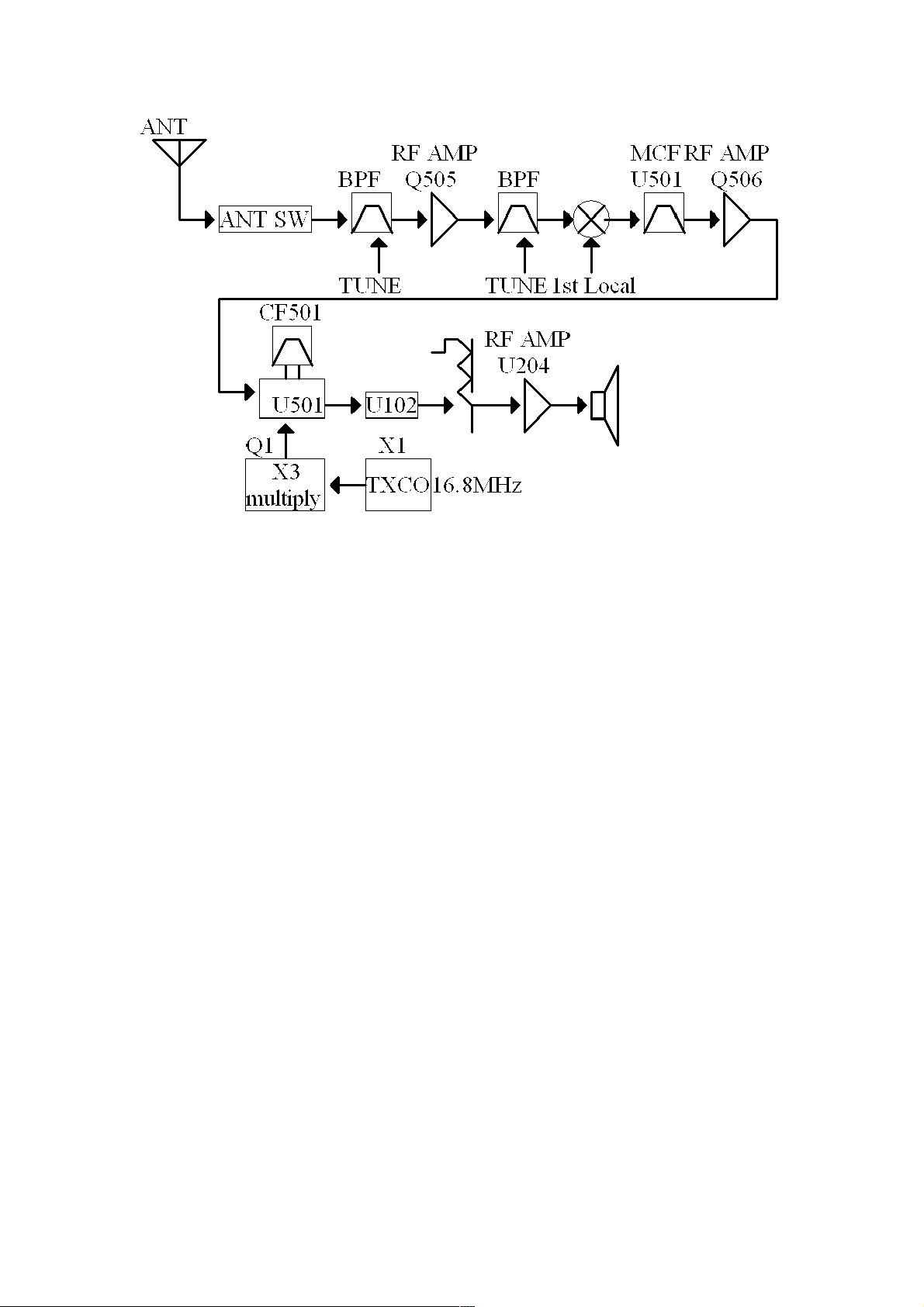
4. wide / narrow switching circuit
t the width and width of each channel by turning on the wide and narrow card switch.
Se
When receiving WIDE (low level) data, Q511 connected.
When receiving NARROW (high) data, Q511 is disconnected.
Q511 is turned on / off with wide / narrow data, the U501 detector output level changes
frequently, with a constant output level that maintains a wide or narrow signal process.
Page 4
as
picture 3 Wide / narrow switching ci
5. Audio amplifier circuit
rcuit
The demodulated signal from U501 is sent to the audio amplifier via U102.The signal is output by AF
volume control and amplified by audio power am
6. Sque
modified by the filter and amplifier to generate the DC voltage corresponding to the noise level.The DC
signal is sent to the analog port (U301) of the microprocessor via the U261. U301 determines whether to
output sound from the speaker by detecting whether the input voltage is higher or lower than the preset
value.When the sound is output from the speaker, U301 sends a high level signal to the SP MUTE line and
turns on the U561.(as picture 4)
lch
part of the AF signal output by the U601 enters the IC, and the noise component is amplified and
A
plifier (U204) to loudspeaker
Page 5
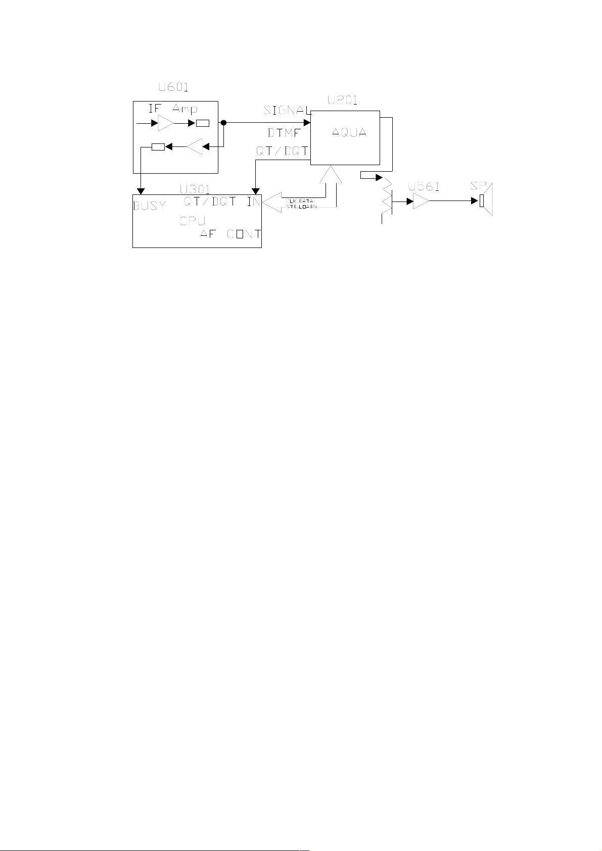
As picture 4 AFamplifier and squelch
7. Receive signaling
1) QT/DQT
The
signal output by U601 enters microprocess (U301) through U201. U301 Determines whether QT or DQT
matches the set value, and controls the SP MUTE and speaker output sound based on this result
2) MSK(Fleet Sync)
The MSK input signal from the FM IC is sent to U201. The signal is mediated in the MSK mediator on
U201. The mediated data is sent to the CPU for processing.
3) DTMF
U601 DTMF output signal to U201. The decoded data has CPU processing.
三、 、 PLL frequency synthesis
The PLL circuit generates the first oscillation signal for reception and the RF signal for emission.
1. PLL
The frequency step of the circuit 5 or 6.25KHz.The output signal of the reference oscillator (VCO) of 16.8MHz is
amplified by Q605 buffer, and then divided by a programmable dual module counter in U601.The frequency division
signals are compared in the corresponding comparators of the U601.The generated signal is filtered through a low-pass
filter and transmitted to the VCO to control the oscillator frequency. (as picture 5)
2. VCO
The frequency used is generated by the Q601 in the transmit mode and is generated by Q603 in the receiving mode.
The oscillation frequency is controlled by feeding the VCO control voltage obtained from the phase comparator to the
shell diode (D607 and D608 in the mode of transmission, D602 and D605 in the reception mode).When receiving, the RX
pin is set to high, so that the Q602 is connected. At launch, the TX pin is set to high, amplifying the Q602 and
transmitting it to the RF amplifier.
Page 6
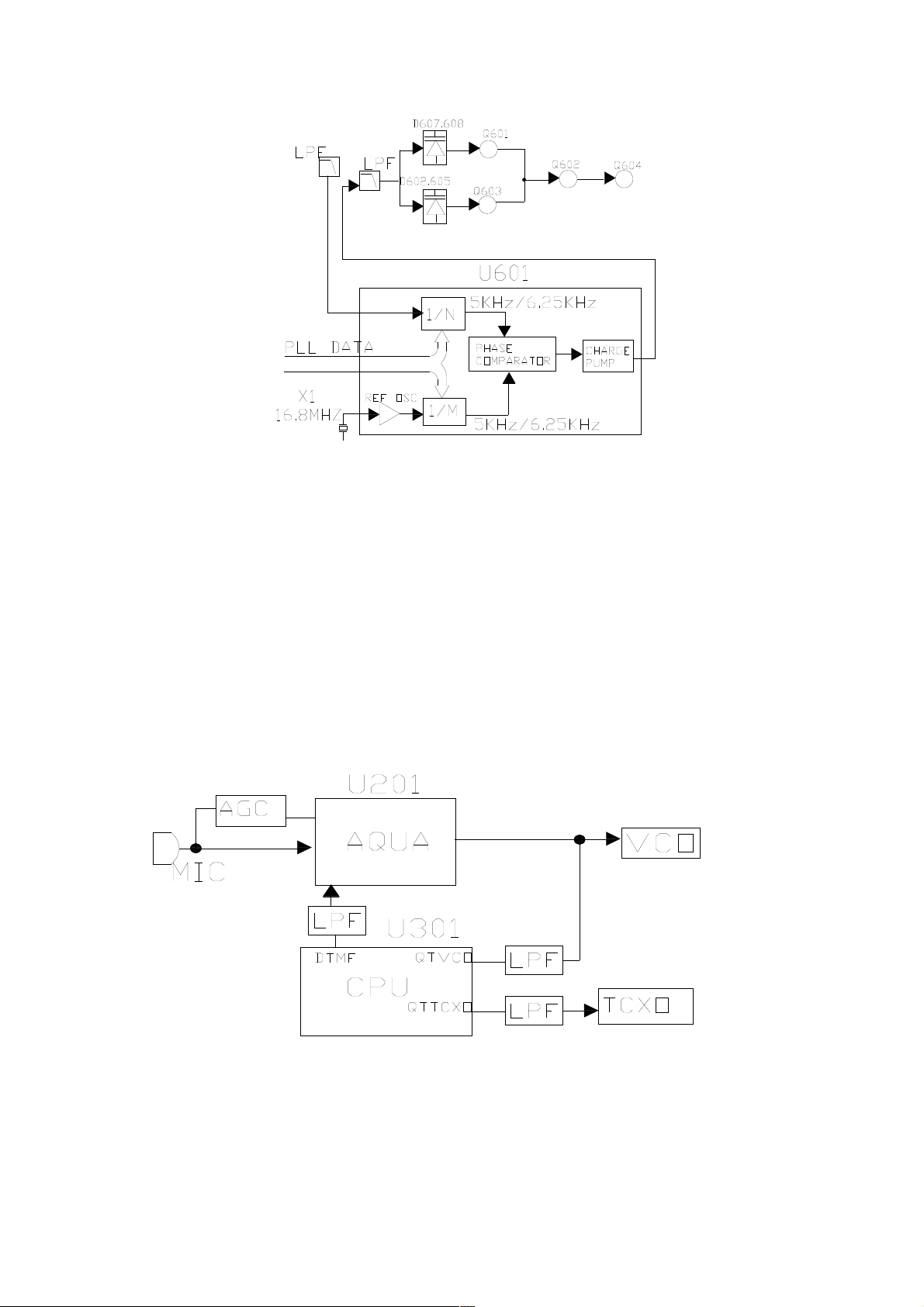
as picture 5 PLL Circuit
3. Lo
and D601 lowers the input voltage of the microprocessor. The microprocessor detects this condition
after the launch is disabled, ignoring the PTT switch input signal.
ss of lock detector
If the pulse signal appears on the PLD pin, a lockout occurs,The DC voltage obtained from C671, R623
4. Tra
nsmitter system
1) Microphone amplifier
he signal from the microphone passes through the U201. When the encoder is DTMF, the input signal of
T
the microphone is closed by U201. The signal is modulated by audio processing (U204), and then sent to VCO
modulation input.
as picture 6 Microphone amplifier
2) Drive and terminal amplifier
T
he signal from the VCO is amplified by the pre-driver amplifier (Q503) and the driver amplifier (Q502)
to 50mW.The output of the driver amplifier is amplified by the RF power amplifier (Q501) to 4.0W (1W at
low power). The RF power amplifier is composed of two MOSFETs. The output of the RF power amplifier is
connected by a harmonic filter (LPF) and an antenna switch ( D501) and sent to the antenna terminal.
Page 7
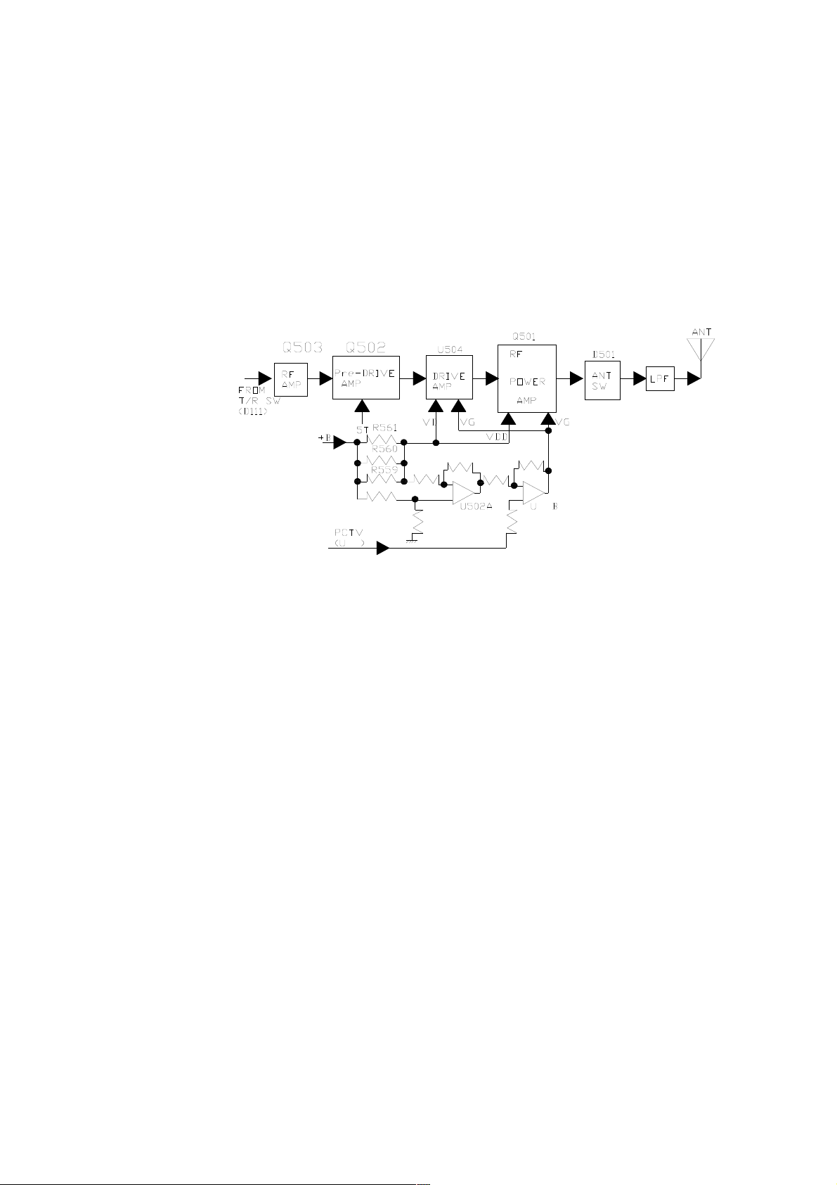
3) Automatic power control (APC) circuit
APC circuit monitors the current through the RF power amplifier (Q501) and keeps the current
The
stable. Changes in the current through the RF power amplifier cause the voltage drop of the R559, R560
and R561 to be sent to the differential amplifier U502A.U502B compares the output voltage of U502A from
the reference voltage of U301.U502B output voltage control RF power amplifier, drive amplifier, pre-drive
amplifier VG, so that the voltage remains the same.
High / low power changes are achieved by changing the reference voltage
502
301
as picture 7 Driver, terminal amplifier and APC ci
5. Po
wer Supply
The machine is powered by 3 5V power supplies to the microprocessor:5C,5R and 5T,At the same
time, when the power is switched on, a 3.3V keeps the output, although the 3.3V is often output,
but when the power is turned off, it is also turned off to prevent the microprocessor from
failure.
5C for the public 5V, in the non-power state to keep the output.
5R is the 5V used for reception and maintains output during reception.
5T is the 5V used for launch and remains output during launch.
rcuit
6. control circuit
Th
e control circuit is composed of microprocessor (U301) and external circuit. The main
functions of U301 are as follows:
a) a) According to the PTT input signal to convert and receive the state.
b) b) Read the system, group, frequency, and programming data from the memory circuit.
c) c) Send the frequency data to the PLL.
d) d) According to the squelch circuit output DC voltage to control the audio mute.
e) e) Control audio mute based on decoded data.
f) f) Launch Tone and programming data.
Page 8
1) Frequency offset circuit
The microprocessor (U301) operates under the 8MHz clock. The oscillator has a circuit that can be converted
to U308 frequency.
If the "Beat Shift" is set to ON, the beat tone can be avoided.
302
as picture 8 Frequency offset circuit
2) Battery low voltage warning
The battery voltage is monitored by the microprocessor and a warning
tone is issued when the warning voltage is lower than the warning
voltage
a) The warning light flashes when the battery voltage is below 6.8V.
b) In the launch, when the battery voltage is below 5.8V, the handset
is forbidden to launch.
c) When the battery voltage drops to less than 5.3V, the hand held
machine.
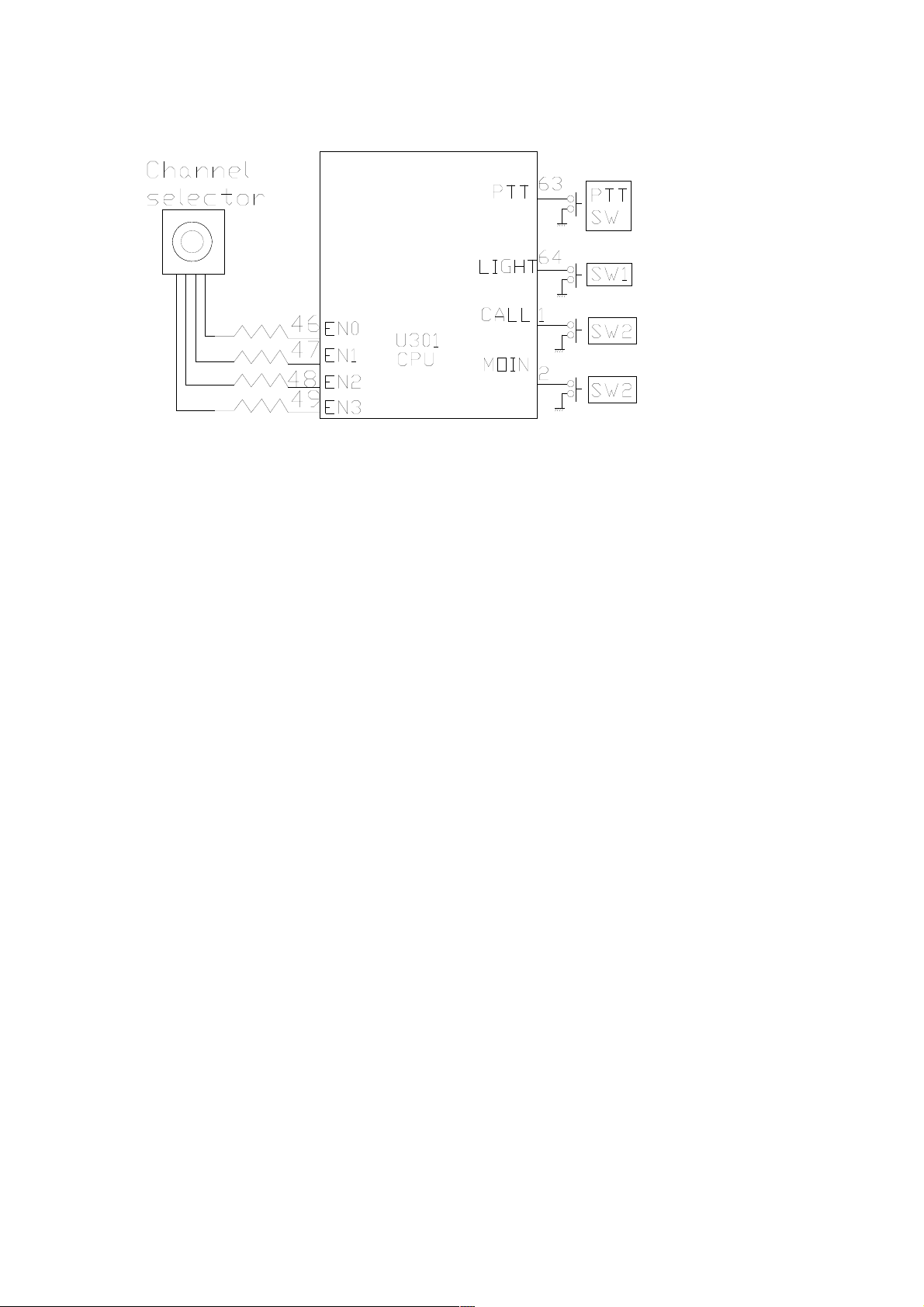
7. Control system
Key and Channel Selector Circuit:
The keys and channel selector signals are input directly to the microprocessor.
Page 9
Page 10

Pin definition
Each pin is assigned as shown in chart 1.
chart 1---CPU pin definition:
Pin Type Name
pin definition Description
1 O PE2 FLASH_CS
FLASH_SCLK/
2 O PE3
LCD_DB6
3 I PE4 FLASH_SDO
FLASH_SDI/
4 O PE5
LCD_DB7
5 O PE6 DMR_SLEEP
6 S VBAT VBAT
7 O PC13 TX_LED
8 O PC14 RX_LED
9 O PC15 LAMP
10 S VSS_5 VSS_5
11 S VDD_5 VDD_5
12 I OSC_IN OSC_IN
13 O OSC_OUT OSC_OUT
14 I RESET RESET
15 I PC0/EXTI0 TIME_SLOT_INTER
Connect the serial FLASH to the first foot CS
Connect serial FLASH sixth pin SCK, multiplexing
to
LCD_DB6
Connect serial FLASH second pin SO
Connect serial FLASH fifth foot SI, multiplexing
o LCD_DB7
t
Connect HR_C5000 forty-seventh pin POWERDOWN; high level effective.
Connect VDD with 0Ω resistor.
TX_LED control; active high.
RRX LED control; active high.
Key backlight control, active high
Connect VSSA.
Connect 3.3V.
Connect 8MHz crystal, 20pF capacitor ground.
With 0Ω resistor, connect 8MHz crystal, 20pF capacitor ground
Connect reset chip; active low. Reserved JTAG RESET
Connect to HR_C5000 at 48 feet TIME_SLOT_INTER
16 I PC1/EXTI1 SYS_INTER
17 I PC2/EXTI2 RF_TX_INTER
PC3/EXTI3/
18 I
RF_RX_INTER
AD123_IN13
19 S VDD VDD
20 S VSS VSS
21 S VREF+ VREF+
22 S VDDA VDDA
PA0/
23 I
MANDOWN
ADC123_IN0
PA1/
24 I
BATT
ADC123_IN1
PA2/
25 I
QT/DQT_IN
ADC123_IN2
PA3/
26 I
VOX
ADC123_IN3
27 S VSS_4 VSS_4
cess to HR_C5000 pin 49 SYS_INTER
Ac
C
onnect to HR_C5000 at 50 feet RF_TX_INTER
onnect HR_C5000 fifty-first foot RF_RX_INTER.
C
onnect 3.3V.
C
onnect VSSA
C
onnect 3.3V.
C
onnect 3.3V.
C
ANDOWN input;
M
attery voltage detection.
B
T/DQT input;
Q
VOX detection input
onnect VSSA
C
28 S VDD_4 VDD_4
29 O PA4/ APC/TV
onnect 3.3V.
C
Transmit power control and receive tuned D / A outputs
Page 11

DAC_OUT1
30 O
MOD2_BIAS
DAC_OUT2
PA6/
PA5/
31 I
POWER_DET
ADC12_IN6
32 O PA7 POWER_C
33 O PC4 RF_APC_SW
34 O PC5 5TC
PB0/
35 I
RSSI
ADC12_IN8
PB1/
36 I
BUSY
ADC12_IN9
BOOT1/
37 I/O PB2/BOOT1
FM_SW
38 O PE7 FM_MUTE
39 O PE8 VCOVCC_SW
40 O PE9 DMR_SW
41 O PE10 VOL_MAX
42 O PE11 MIC_SW
Co
ntrols the TCXO reference frequency D / A
output
wer switch input.
Po
wer on control; active high.
Po
RF amplifier switch control; active high.
power control, active high.
5T
SI detection input.
RS
USY detection
B
T
he default 10K resistor is grounded.
F
M receive channel mute control.
RXVCO / TXVCO power control.
MR receive IF path switch control
D
aximum volume control, active high.
M
I
nternal MIC mute control, high level INT_MIC.
43 I PE12 PTT_KEY
44 I PE13 ALARM_KEY
45 I PE14 ENCODE_IN0
46 I PE15 ENCODE_IN1
47 I PB10 ENCODE_IN2
48 I PB11 ENCODE_IN3
49 S VCAP_1 VCAP_1
50 S VDD_1 VDD_1
PB12/
51 O
DMR_CS
SPI2_NSS
PB13/
52 O
DMR_SCLK
SPI2_SCK
PB14/
53 I
DMR_SDO
SPI2_MISO
PB15/
54 O
DMR_SDI
SPI2_MOSI
55 I PD8 PLL_LD
56 O PD9 PLL_CS
57 O PD10 PLL_DAT
TT key input
P
larm key input
A
hannel coding input 0
C
hannel coding input 1
C
hannel coding input 2
C
hannel coding input 3
C
E
xternal capacitor to ground.
onnect 3.3V.
C
onnect to HR_C5000 at pin 58 U_CS.
C
C
onnect to HR_C5000 at pin 57 U_SCLK
onnect to HR_C5000 at pin 55 U_SDO
C
onnect to HR_C5000 at pin 56 U_SDI
C
LL lock detection, high when locked.
P
LL enable control
P
P
PLL_DAT output control
58 O PD11 PLL_CLK
LL_CLK clock pin
P
59 O PD12 LCD_RES LCD_RES
Page 12

60 O PD13 LCD_A0 LCD_A0
61 O PD14 LCD_CS1 LCD_CS1
62 O PD15 FL_C
Fast lock voltage output control, active high
63 O PC6/TIM8_CH1 FAST_LOCK
64 O PC7/TIM8_CH2 CTC/DCS_OUT
65 O PC8/TIM8_CH3 BEEP
66 O PC9 5RC
67 O PA8 SAVE
PA9/
串口TXD/
68 I/O
USART1_TX
PA10/
SELC
串口RXD/
69 I
USART1_RX
EXT_PTT
70 I/O PA11/USBDM USBD-
71 I/O PA12/USBDP USBD+
JTMS-SWDIO/
SWDIO/
72 I/O
PA13
WORN_SW
73 S VCAP_2 VCAP_2
74 S VSS_2 VSS_2
75 S VDD_2 VDD_2
Fast lock voltage output control, active high.
/ DCS PWM output to TCXO
CTC
/ ALARM / DTMF PWM output
BEEP
5R power control, active high.
5C power supply power control; active high.
Reserved Bootloader TX; Alternate external access control
input, then the first part of the external accessories.
Reserved Bootloader RX; multiplexed external
PTT input, external accessory pin 9.
USB data cable DM, then the external accessories 5 feet
USB data cable DP, access to external accessories 4 feet.
served JTAG interface.
Re
ternal capacitor to ground.
Ex
ound
Gr
nnect 3.3V.
Co
JTCK-SWCLK/
SWCLK/
76 I/O
PA14
MANDOWN_SW
PA15/
77 O
I2S_FS
I2S3_WS
PC10/
78 O
I2S_CK
I2S3_CK
PC11/
79 O
I2S_RX
I2S3ext_SD
PC12/
80 I
I2S_TX
I2S3_SD
81 I/O PD0 K2
82 I/O PD1 K3
83 I/O PD2 K4
84 I/O PD3 K5
85 I/O PD4 K6
86 I/O PD5 K7
87 I/O PD6 K8
88 O PD7 V_CS
served JTAG interface; multiplexed access
Re
to external accessories 12 feet.
Co
nnect to HR_C5000 pin 37 I2S_FS
C
nnect the HR_C5000 to the 36th foot I2S_CK
o
nnect HR_C5000 pin 34 I2S_RX
Co
nnect HR_C5000 to pin 35 I2S_TX
Co
Pr
ess key K2 to enter
ess key K3 to enter
Pr
ess key K4 to enter
Pr
Pr
ess key K5 to enter
Press key K6 to enter
Pr
ess key K7 to enter
Pr
ess key K8 to enter
Connect HR_C5000 to pin 44 V_CS
89 O
PB3/
SPI3_SCK
V_SCLK
Co
nnect the HR_C5000 to the 43rd pin V_SCLK
Page 13

90 I
PB4/
SPI3_MISO
V_SDO
nect HR_C5000 to pin 42 V_SDO
Con
91 O
V_SDI
SPI3_MOSI
92 O PB6 SELECT
93 O PB7 MODE
94 I BOOT0 BOOT0
PB8/
PB5/
95 O
SCL
I2C1_SCL
PB9/
96 O
SDA
I2C1_SDA
97 O PE0 K0
98 O PE1 K1
99 S VSS_3 VSS_3
100 S VDD_3 VDD_3
nect HR_C5000 to pin 41 V_SDI
Con
Internal external audio output selection, high level external.
Audio amplifier control, high level open.
The default 10K pull-down resistor is grounded.
nnect the chip to the third pin, an external
Co
pull-up resistor to 3.3V.
Connect the encryption chip pin 4, external
pull-up resistor to 3.3V.
Pre
ss key K0 to enter
ess key K1 to enter
Pr
round
G
onnect 3.3V.
C
Page 14

chart 2--- CPU pin Port definition:
Pin
Pin Type Name
definition
Exp
lain
23 I
MANDOWN
ADC123_IN0
PA1/
PA0/
24 I
BATT
ADC123_IN1
PA2/
25 I
QT/DQT_IN
ADC123_IN2
PA3/
26 I
VOX
ADC123_IN3
PA4/
29 O
APC/TV
DAC_OUT1
PA5/
30 O
MOD2_BIAS
DAC_OUT2
PA6/
31 I
POWER_DET
ADC12_IN6
32 O PA7 POWER_C
67 O PA8 SAVE
PA9/
串口TXD/
68 I/O
USART1_TX
PA10/
SELC
串口RXD/
69 I
USART1_RX
EXT_PTT
70 I/O PA11/USBDM USBD-
served) MANDOWN input;
(Re
Batt
ery voltage detection; the maximum input
voltage of 2.8v.
DQT input
QT/
VOX detection input
ansmit power control and receive tuned
Tr
D / A outputs
ontrols the TCXO reference frequency D /
C
A output
ower switch input, high level indicates
P
that the power is turned on.
ower on control; active high.
P
5
C power supply power control; active high.
Reserved Bootloader TX; Alternate external access control
input, then the first part of the external accessories.
Reserved Bootloader RX; multiplexed external PTT input,
external accessory pin 9.
SB data cable DM, then the external
U
accessories 5 feet.
71 I/O PA12/USBDP USBD+
JTMS-SWDIO/
SWDIO/
72 I/O
PA13
JTCK-SWCLK/
WORN_SW
SWCLK/
76 I/O
PA14
MANDOWN_SW
PA15/
77 O
I2S_FS
I2S3_WS
PB0/
35 I
RSSI
ADC12_IN8
PB1/
36 I
BUSY
ADC12_IN9
BOOT1/
37 I/O PB2/BOOT1
FM_SW
PB3/
89 O
V_SCLK
SPI3_SCK
USB data cable DP, access to external accessories 4
feet.
Reserved JTAG interface; multiplexed with external accessories
pin 2. Reserved wide and narrowband to receive volume switching,
Reserved JTAG interface; multiplexed access to external
accessories 12 feet. Reserved MANDOWN power switch, active
The default 10K resistor is grounded. Used as output port,
the default working state is 0, reduce power consumption.
Multiplexed for FM reception IF channel switch control;
C
onnect the HR_C5000 to the 43rd pin V_SCLK
high level for broadband.
high.
C
onnect to HR_C5000 pin 37 I2S_FS
SSI detection input
R
USY detection
B
active high.
Page 15

90 I
PB4/
SPI3_MISO
V_SDO
Connect HR_C5000 to pin 42 V_SDO
91 O
V_SDI
SPI3_MOSI
92 O PB6 SELECT
93 O PB7 MODE
PB8/
PB5/
95 O
SCL
I2C1_SCL
PB9/
96 O
SDA
I2C1_SDA
47 I PB10 ENCODE_IN2
48 I PB11 ENCODE_IN3
PB12/
51 O
DMR_CS
SPI2_NSS
PB13/
52 O
DMR_SCLK
SPI2_SCK
PB14/
53 I
DMR_SDO
SPI2_MISO
PB15/
54 O
DMR_SDI
SPI2_MOSI
15 I PC0/EXTI0 TIME_SLOT_INTER
Connect HR_C5000 to pin 41 V_SDI
Internal external audio output selection, high level external.
Audio amplifier control, high level open
Conn
ect the chip to the third pin, an external
pull-up resistor to 3.3V.
n
ect the encryption chip pin 4, external
Con
pull-up resistor to 3.3V.
Channel code input 2
Channel code input 3
ect the HR_C5000 58th U_CS, an external
Conn
pull-up resistor to 3.3V.
nect to HR_C5000 at pin 57 U_SCLK
Con
Co
nnect to HR_C5000 at pin 55 U_SDO
Co
nnect to HR_C5000 at pin 56 U_SDI
Connect to HR_C5000 at 48 feet TIME_SLOT_INTER
16 I PC1/EXTI1 SYS_INTER
17 I PC2/EXTI2 RF_TX_INTER
PC3/EXTI3/
18 I
RF_RX_INTER
AD123_IN13
33 O PC4 RF_APC_SW
34 O PC5 5TC
63 O PC6/TIM8_CH1 FAST_LOCK
64 O PC7/TIM8_CH2 CTC/DCS_OUT
65 O PC8/TIM8_CH3 BEEP
66 O PC9 5RC
PC10/
78 O
I2S_CK
I2S3_CK
PC11/
79 O
I2S_RX
I2S3ext_SD
PC12/
80 I
I2S_TX
I2S3_SD
7 O PC13 TX_LED
nnect to HR_C5000 pin 49 SYS_INTER
Co
Co
nnect to HR_C5000 at 50 feet RF_TX_INTER
Connect HR_C5000 pin 51 RF_RX_INTER. Reserved
fo
r 2T / 5T / DTMF input detection.
RF
amplifier switch control; active high.
5T
power control, active high.
st lock voltage PWM output
Fa
C / DCS PWM output to TCXO
CT
EP / ALARM / DTMF PWM output
BE
power control, active high.
5R
Co
nnect the HR_C5000 to the 36th foot I2S_CK
C
onnect HR_C5000 pin 34 I2S_RX
C
onnect HR_C5000 to pin 35 I2S_TX
X_LED control; active high.
T
8 O PC14 RX_LED
9 O PC15 LAMP
X LED control; active high.
R
ey backlight control, active high
K
Page 16

81 I/O PD0 K2
82 I/O PD1 K3
83 I/O PD2 K4
84 I/O PD3 K5
ss key K2 to enter
Pre
Pre
ss key K3 to enter
Pre
ss key K4 to enter
ss key K5 to enter
Pre
85 I/O PD4 K6
86 I/O PD5 K7
87 I/O PD6 K8
88 O PD7 V_CS
55 I PD8 PLL_LD
56 O PD9 PLL_CS
57 O PD10 PLL_DAT
58 O PD11 PLL_CLK
Pre
ss key K6 to enter
ss key K7 to enter
Pre
ss key K8 to enter
Pre
nect HR_C5000 to pin 44 V_CS
Con
PLL lock detection, high when locked.
PLL enable control
PLL_DAT output control
_CLK clock pin
PLL
59 O PD12 LCD_RES LCD_RES
60 O PD13 LCD_A0 LCD_A0
61 O PD14 LCD_CS1 LCD_CS1
62 O PD15 FL_C
97 O PE0 K0
98 O PE1 K1
1 O PE2 FLASH_CS
FLASH_SCLK/
2 O PE3
LCD_DB6
Fast lock voltage output control, active high.
ss key K0 to enter
Pre
ss key K1 to enter
Pre
Con
nect the serial FLASH to the first foot CS
nect the serial FLASH 6th SCK, multiplexed
Con
with LCD_DB6
3 I PE4 FLASH_SDO
FLASH_SDI/
4 O PE5
LCD_DB7
5 O PE6 DMR_SLEEP
38 O PE7 FM_MUTE
39 O PE8 VCOVCC_SW
40 O PE9 DMR_SW
41 O PE10 VOL_MAX
42 O PE11 MIC_SW
43 I PE12 PTT_KEY
44 I PE13 ALARM_KEY
45 I PE14 ENCODE_IN0
46 I PE15 ENCODE_IN1
Con
nect Serial Flash 2nd Foot SO
Connect the serial FLASH pin 5, multiplexed to
LCD_DB7
Connect HR_C5000 47th POWERDOWN; active
h
igh. External pull-up resistor to 3.3V.
FM receive channel mute control; active high.
RXVCO / TXVCO power control.
DMR receive IF channel switch control, active high.
Ma
ximum volume control, active high.
I
ternal MIC mute control, active high.
n
T key input
PT
arm key input
Al
annel code input 0
Ch
annel code input 1
Ch
Page 17

BOM
parameter
16.8MHz
1XTV16800CFA
3225
1
X601
1SR154-400
D1210
1
D402
1SS372
1SS372
3
D101 D114-115
29.4912MHz
1XTW29491CAA
3225
1
X201
2SA1586
2SA1586
1
Q105
2SC3356
SOT-23
4
Q503-504 Q601 Q603
PBR951
SOT-23
2
Q507 Q509
2SC4116 2SC4116 1 Q103
KTC4075
2SJ243
2SJ243
2
Q101 Q607
2SK1824
SOT-523
1
Q104
ELFY450H 450KHZ 1 CF501
LTWC450H
8MHz
1C208000BB0B
3225
1
X301
AD2736
SOT23-6
1
U401
SKY72310
SKY72310-S62LF
QFN-24
1
U601
SKRTLAE010
SKRTLAE010
ALARM-PX780
1
SW301
HR_V3000S/ALPU-MP
HR_V3000S/ALPU-MP
SOT23-6
1
U307
AT41511
AT41511
1
Q505
BATTERY-CON
CBC47S13D
CBC47S13D
1
J401
BLM21PG221S BLM21PG221S L0805 3 L201 L522 L545
PB201209-221
0P5
402
2
C608-609
100P 402 19
C152-159 C161 C525 C527 C580 C654 C656-659 C678
C681
102 402 19
C105-106 C108 C125 C233 C248 C256 C287 C314-315
C404 C410 C523 C555 C584 C594 C639 C649 C711
specification
Package
Quantity
Element bit number Additional information
Page 18

103 402 57
C102 C126 C131 C141-142 C144-145 C150 C162 C182
C185 C227 C237 C270 C272 C276 C278 C280 C282 C284
C312-313 C316-319 C339 C345 C420 C422 C424 C427
C430 C433 C436 C532 C534-537 C540 C544 C546 C557
C585 C597 C644 C646 C655 C672 C675 C694 C706 C713
C718 C722 C724
104 402 64
C115 C130 C133 C135 C160 C225-226 C230 C232 C235
C239-240 C252 C264 C267 C273-274 C285 C290 C305-307
C310-311 C320 C338 C346 C350 C360-362 C405-407 C413
C421 C428 C432 C435 C438 C520 C547-548 C551-552
C559 C571 C577 C583 C595-596 C610 C613 C615 C627
C630 C637-638 C663 C665 C676 C682 C690 C709
105 402 51
C114 C117-121 C129 C132 C134 C136-138 C146 C148-149
C163 C168 C180-181 C183-184 C190 C224 C238 C249-250
C258 C260 C269 C271 C279 C281 C283 C308 C337 C343-
344 C352 C412 C415-416 C419 C423 C666 C674 C680
C683 C685 C691 C710 C712
10P
4025C231 C514 C635-636 C716
123
402
1
C124
12P
402
4
C513 C541-542 C574
153
402
2
C332 C686
180P
402
1
C645
183
402
4
C139 C333 C336 C677
1P5
402
3
C614 C617 C631
220P 402 13
C101 C110 C128 C188 C241 C244 C259 C261 C553-554
C721 C723 C725
222
402
1
C123
223
4026C107 C112 C408 C549 C556 C109
22P
402
1
C529
27P
402
1
C579
270P
402
4
C263 C265-266 C268
120p
402
1
C550
2P
402
2
C515 C689
Page 19

332
402
4
C295-296 C640 C687
333
402
1
C257
33P
402
3
C518 C545 C647
392
402
1
C335
393
402
1
C127
3P
4026C509 C524 C697 C699 C660-661
470P 402 38
C113 C164-166 C172 C253 C401 C449 C521 C533 C538
C560-561 C563 C566 C570 C572-573 C578 C582 C598
C611-612 C616 C619 C628-629 C634 C662 C667 C669-670
C673 C684 C693 C704 C707 C719
473
402
2
C653 C705
47P
402
3
C147 C519 C643
56P
402
1
C708
5P
402
2
C517 C530
682P
402
2
C170-171
683
402
1
C122
68P
402
1
C648
6P
4025C510 C531 C568 C618 C632
7P
402
2
C539 C696
822
402
2
C140 C143
8P
402
4
C302-303 C516 C633
9P
402
3
C564 C698 C526
104
TC212P104M035A
C0805
2
C650 C652
10U/10V GRM21BR71A106KE51L C0805 4 C228 C236 C291 C451
GRM21BR61A106KE1
9L
2.2U/10V
GRM21BR71A225KE51L
C0805
1
C437
太诱
105
603
1
C692
10P
603
2
C606 C591
120P
603
1
C507
12P
603
2
C592 C625
15P
603
3
C587-588 C590
18P
603
2
C605 C624
1P5
603
1
C503
Page 20

27P
603
1
C589
2P
603
1
C505
39P
603
1
C607
3P
603
2
C501 C506
47P
603
2
C586 C626
4P
603
1
C621
68P
603
1
C593
6P
6035C502 C504 C601-602 C620
7P
603
1
C623
8P
603
1
C604
4.7U/10V GRM21BR71A475KE51L C0805 1 C664
GRM21BR61A475KA7
3L
22U/10V GRM31CR71A226ME15L C1206 6 C286 C409 C425 C441 C450 C599
钽电容(A)
10U/10V
TEESVP1A106M8R
C0805T
2
EC104 EC558
10uF/10V
TEESVP1A106M8R
C0805T4EC431 EC434 EC668 EC671
黑色钽电容
1uF/16V
TEESVP1C105M8R
C0805T
2
EC167-168
2.2uF/10V
TEESVP1A225M8R
C0805T
2
EC151 EC651
4.7uF/10V
TEESVP1A475M8R
C0805T
1
EC103
10uF/16V
TEESVA1C106K8R
C1206T
1
EC403
黑色钽电容
22uF/10V
TEESVA1C226K8R
C1206T
1
EC262
GRM31CR61A226KE19代
EXT_JACK
AXK5F20547YG
CON20
1
J102
KEYPAD_JACK
AXK6F20547YG
CON20
1
J101
49.95MHz
1D49910GQ9
7X5
1
XF501
KDS114E
D0603
4
D503-504 D510-511
KDS160E
D06035D403-404 D406-407 D601
BV08C
D04029D103-104 D106-107 D109-113
1SV278
D0603
1
D610
1SV305
D0603
8
D602-609
HVC350B
D0603
4
D505-507 D513
DTC144EE
SOT-523
9
Q102 Q201-203 Q206 Q301-302 Q402 Q510
CODE-SWITCH
ED10308O
ED08C030
1
SW302
3AFUSE F1206-F 1 F401
0466003.NRHF
Page 21

3.3uH MLF1608A3R3K 603 1 L601
CI160808-3R3K叠
470nH MLF1608AR47KT000 603 2 L514 L608
CI160808-R47K叠
560nH MLF1608DR56KT 603 2 L513 L607
CI160808-R56K叠
JTBM450CX24
CD-450KHZ
1
FD501
FMMT717
FMMT717A
1
Q401
PNP,SOT23
HR_C5000
QFP80-9
1
U201
1SS362
HSM88AS
1
D512
BA592
HVU131
1
D501
0R
6035L520 L547 L105 L546 L106
12nH
LQW18AN12NJ00D
603
2
L626-627
绕线
18nH LQW18AN18NJ00D 603 1 L602
HWI0603UC18NG绕
2.7nH MLG1608B2N7S 603 1 L523
CH160808-2N7S叠
22nH MLG1608B22NJ 603 6 L508 L518-519 L533 L617 L625
CH160808-22NJ叠
330nH
MLG1608SR33J
603
1
L609
叠层
330nH LQW18ANR33J00D 603 6 L614-616 L622-624
HWI0603UCR33J绕
33nH LQW18AN18NJ00D 603 2 L612 L620
HWI0603UC33NG绕
390nH LQW18ANR39J00D 603 2 L611 L619
HWI0603UCR39J绕
47nH LQW18AN47NJ00D 603 1 L515
HWI0603UC47NG绕
82nH MLG1608B82NJ 603 1 L509
CH160808-82NJ叠
1uH NL252018T-1R0J L2520 1 L501
NLV25T-1R0J模压
电感
10uH SWPA3012S100MT L3030 1 L404
SWPA3012S100MT
47uH SWPA3012S470MT L3030 1 L203
SWPA3012S470MT
BLM18AG601S BLM18AG601S 603 13
L101-104 L202 L208 L401 L528 L531 L603 L610 L630
L666
CB160808-601
10nH LQW2BHN10NJ03L L0805 1 L613
HWI0805UC10NG顺
绕白色
15nH LQW2BHN15NJ03L L0805 1 L621
HWI0805UC15NG顺
绕白色
1uH C2012C1R0J L0805 1 L521
HWI0805UC1R0J绕
220nH C2012CR22J L0805 1 L527
HWI0805UCR22J绕
2T
ER0.35×1.6×2
2T
1
L526
Page 22

3T
ER0.35×1.6×3
3T
3
L502 L504-505
4T
ER0.35×1.6×4
4T
1
L503
5T
EL0.31*1.2*5T
5T 4 L506-507 L511 L530 正绕平角
8T
ER0.35×1.6×8
8T
1
L524
GREEN
D0603
2
LED301-302
RED
D0603
1
LED303
RD01MUS2 RD01MUS2 SOT-89 1 Q502
RD01MUS1
RD07MUS2B
RD07MUS2B-T112
RD07MUS2B
1
Q501
3SK318
SC82AB
1
Q506
NJM2100V
SOP-8
1
U103
NJM2904V
SOP-8
2
U502 U603
2SC4617(S)
SOT-523
1
Q606
2SC5066(Y)
SOT-5234Q602 Q604-605 Q608
DTA143ZETL
SOT-523
1
Q511
PST9124
SOT-23-5
1
U303
0R
4026R160 R320 R334 R507 R565 R258
1.5M
402
2
R567 R702
100K 402 26
R107 R113-114 R118 R121 R128-129 R133 R151 R154
R244 R310 R402 R418 R501-503 R510 R513 R581 R599
R644-645 R650-651 R659
100R
402
9
R517-518 R571 R604 R614 R627 R629 R642-643
10K 402 30
R115 R117 R132 R135 R150 R231-234 R240 R259 R262
R266-268 R306 R311 R313 R321 R342 R360-361 R419
R422 R446 R631-632 R637-638 R652
10R
402
8
R229 R263 R269-270 R528 R609 R630 R634
120R
402
2
R603 R613
12K
402
1
R143
150K
402
3
R124 R138 R621
150K1%
402
4
R562 R564 R566 R701
15K
402
3
R335 R605 R549
15R
402
1
R537
180K
4026R126-127 R261 R265 R525 R606
180R
402
3
R314 R512 R635
Page 23

18K
402
3
R111 R134 R648
1K 402 29
R102 R153 R225 R236 R238 R253 R301 R308-309 R332333 R351-353 R355-358 R370 R391 R520 R530 R533 R535
R542 R545 R608 R628 R149
1K5
402
2
R411 R551
1K8
402
3
R108 R522 R555
1M
402
1
R141
2K2
4025R341 R406 R515 R526 R570
200K
402
1
R401
20K
402
2
R241 R552
220K
402
4
R131 R147 R243 R572
220R
402
1
R315
22K
4027R125 R148 R336 R340 R425 R539 R615
22R
402
4
R106 R120 R543 R548
270K
402
1
R145
270R
402
1
R568
27K
402
3
R524 R569 R703
2K7
402
1
R156
330K
402
2
R639 R527
330R
402
2
R508 R619
33K
402
1
R123
390K
402
1
R146
390R
402
2
R556 R595
3K3
402
2
R142 R305
3K9
402
1
R617
470K
4027R112 R136 R144 R155 R413-415
470R
4025R104 R521 R531 R640 R658
47K
402
11
R122 R312 R316-319 R354 R405 R408 R550 R574
47R
402
2
R516 R554
4K7 402 15
R338-339 R362-363 R412 R523 R541 R547 R588 R602
R612 R620 R623 R646 R680
560
402
2
R157-158
560K
402
2
R519 R641
Page 24

56K
402
2
R511 R514
56R
402
1
R636
5K6
4027R139-140 R505 R575 R601 R611 R616
68K
402
3
R137 R410 R622
6K8
402
2
R506 R546
750K
402
1
R529
820K
402
1
R116
820R
402
1
R152
82K
402
2
R130 R553
8K2
402
2
R536 R538
9K1
402
1
R649
0.39R
R1206
3
R559-561
STM32F405VGT6
LQFP100
1
U301
VOL-SWITCH
R08710NS
AEC15C7
1
SW401
GT3136
SSOP-N16
1
U501
TC75S51F
SOT-23-5
1
U203
TDA8547TS
SSOP-N20
1
U204
NJM2902V
SSOP14
2
U101-102
UMC4N
UMC4
4
U104 U503 U505 U604
W25Q80DVSIG
W25Q80DVSIG
1
U302
XBS104S13R-G XBS104S13R-G 1 D405
XBS053V15R-G
XC6204B332MR
SOT-23-5
1
U602
XC6204B502MR
SOT-23-5
4
U105 U404-406
XC6204B602MR
SOT-23-5
1
U402
L501 molded inductors (L1008)
Note:
L614 330NH Winding with blue, the other can be changed white plastic.
AMBE vocoder
Page 25

Page 26

Page 27

Page 28

Page 29

Q606x1Q606x2 Q606x3
Q606
H1x1
H1x2
H1x8
H1x3
H1
H1x7
H1x4
H1x6
H1x5
H1x9
S17
S13
S9
S10
S17x1
S17x2
LED1x1
LED1x2
LED1
S13x1
S13x2
S9x1
S9x2
LED3
S10x1
S10x2
LED3x1
LED3x2
S14
S5
S6
S14x1
S14x2
S5x1
S5x2
LED4
S6x1
S6x2
LED2x1
LED2
LED4x1
LED4x2
S16
LED2x2
S15
S1
S2
S16x1
S16x2
S15x1
S15x2
S1x1
S1x2
S2x1
S2x2
H2x1
H2x2
H2x8
H2x3
H2
H2x7
H2x4
H2x6
H2x5
H2x9
H3x1
H3x2
H3x8
H3x3
H3
H3x7
H3x4
H3x6
H3x5
H3x9
S11
S12
S11x1
S11x2
LED5
S12x1
S12x2
LED5x1
LED5x2
S7
S8
S7x1
S7x2
S8x1
S8x2
LED6x1
LED6
LED6x2
S3
S4
S3x1
S3x2
S4x1
S4x2
H4x1
H4x2
H4x8
H4x3
H4
H4x7
H4x4
H4x6
H4x5
H4x9
Page 30

J2
J2x1
R22x1R22x2
R23x1R23x2
R24x1R24x2
R22
R23
R24
J2x2
J2x3
J2x4
J2x5
R13x1R13x2
R14x1R14x2
R13
R14
J2x6
J2x7
J2x8
C9x1C9x2
C9
R16
J2x9
J2x10
C8x1C8x2
C8
R16x1 R16x2
J2x11
J2x12
C7x1C7x2
C6
C7
J2x13
C5
C6x1 C6x2
J2x14
J2x15
C5x1C5x2
C4
J2x16
J2x17
C3x1C3x2
C4x1C4x2
C2
C3
J2x18
C2x1C2x2
C1
C1x1C1x2
R25x2
R25
R26x2
R26
R25x1
Q606x1Q606x2 Q606x3
Q606
R26x1
H1x1
H1x2
H1x8
H1x3
H1
H1x7
H1x4
H1x6
H1x5
H1x9
C14x1
C14x2
C14
C13x1
C12x2
C12
U1x4 U1x5
C17x1
C13x2
C12x1
C17x2
C13
U1
C17
U2
R17x1
R17
R19x1
R19
R18x1
R18
R21x2
R21
R10x1
R10
R11x1
R11
R12x1
R12
U1x1U1x2U1x3
C10
C11
C10x1 C10x2
C11x1 C11x2
R15x1
R15x2
R15
C15x1
C15x2
C15
U2x4 U2x5
R20x1R20x2
R17x2
R20
R19x2
R18x2
C16
C16x1 C16x2
R21x1
R10x2
R11x2
R1
R12x2
U2x1U2x2U2x3
R1x1R1x2
R2x1R2x2
R2
R3
J1x1
R3x1R3x2
J1x2
J1x3
J1x4
R5x1R5x2
R4x1R4x2
R5
R6
R4
J1x5
J1x6
J1x7
J1x8
R6x1R6x2
R7
J1x9
J1x10J1x11
R7x1R7x2
R8x1R8x2
R8
R9
H2x3
H2
R9x1R9x2
H2x1
H2x2
H2x8
H2x7
H2x4
H2x6
H2x5
H2x9
H3x1
H3x2
H3x8
H3x3
H3
H3x7
H3x4
H3x6
H3x5
H3x9
J1
J1x12
J1x13
J1x14
J1x15
J1x16
J1x17
J1x18
J1x19
J1x20
H4x1
H4x2
H4x8
H4x3
H4
H4x7
H4x4
H4x6
H4x5
H4x9
Page 31

R25
R26
10R
10R
LCD
LCD
LCD1
C1
105
C2
105
C3
105
C4
105
C5
105
101112131415161718
C6
104
LCD_RES
LCD_A0
LCD_DB6
LCD_DB7
VDD
C7
104C8
NC
0R
R16
C9
105
123456789
LCD_CS1
LED11
BACKLIGHT
BACKLIGHT LED
R17
R18
390R
390R
LED12
BACKLIGHT
R19
390R
J1
123456789
AXK5F20347YG
K0K1K2K3K4K5K6K7K8
R24 1K
R23 1K
R22 1K
R14 1K
R13 1K
1011121314151617181920
LCD_CS1
LCD_RES
LCD_A0
LCD_DB6
LCD_DB7
+BAT7V5
1
U1
XC6204B332MR
5
C11
C10
4K7
R15
VIN2VSS
OUT4NC
C12
C13
C14
105
105
3
CE
105
10U/10V
103
1
VIN2VSS
U2
OUT4NC
XC6204B502MR
5
LAMP
C15
105
C16
R20
4K7
3
CE
C17
105
R21
22R
470P
R10
220R
GREEN
GREEN
LED1
LED2
R11
220R
GREEN
GREEN
LED3
LED4
R12
220R
GREEN
GREEN
LED5
LED6
R81KR9
R2
R1
1K
#
S4
9
S3
6
S2
3
S1
1K
S8
S7
S6
S5
R3
1K
0
8
5
2
S12
S11
S10
S9
R4
1K
*
7
4
1
S16
S15
S14
S13
S17
R-SHIFT
BACK
OK
MENU
L-SHIFT
R5
1K
R61KR7
1K
1K
9
9
9
9
8
123
8
123
8
123
8
123
6
7
H4
Hole
4 5
6
7
H3
Hole
4 5
6
7
H2
Hole
4 5
6
7
H1
Hole
4 5
Page 32

RDR3600-VHF-V5.2
2015-02-02
10P
20K
27P
15K
0R
9P
3P
3P
330K
1K8
120P
1K8
Page 33

RDR3600-VHF-V5.2
220K
2015-02-02
0R
0R
223P
0R
682P
682P
3K3
2
1K
Page 34

SW401
C409
C409
C409x2
C410
C410x2
C410
H10x1
H10x2
H10x8
C406
C406x2
C406
H10
H10x3
H10x7
H10
H8x3
H8
H6x3
H6
C450
H10x4
H10x6
H10x5
H10x9
L401
C450
C450x1 C450x2
R412x1R412x2
R412
C416
R412
C416x1
C416x2
C416
R425
U401x4U401x5U401x6
U401
U401
U401x1 U401x2 U401x3
C408
C408x1
C408
R411
R411x1
R411
D405
D405xA D405xK
D405
R410
C424
R410x1 R410x2
R410
L404
L404
L404x1 L404x2
C413
C413x2
C413
C425
C425
C425x1
C441
C441
C441x1
C427
C427x1
C427
C412
C412x1
C412x2
C412
R413x1R413x2
R413
U404x1
U404x2
U404x3
R413
U404
U404
U404x4
U404x5
EC431
R420
EC431x1
EC431x2
EC431
R420
C432
C432x1
C432x2
C430
C432
H8x1
H8x2
H8x8
H8
H8x7
H8x4
H8x6
H8x5
H8x9
C622x1C622x2
L621
C622
L621x1
L621
C622
C623
C623x1
C623x2
C623
C624
C621x1C621x2
C620x1C620x2
C624
C621
C620
C621
C620
C626
D602x1D602x2
D603x1D603x2
L620x1L620x2
L620
D603
D602
D602
D603
C625
L620
D605
D605x1
D605x2
D605
L619x1L619x2
D604
D604x1
D604x2
D604
L619
L619
C654x1
C654x2
C654
C654
R602
L611
C653
C653x1 C653x2
C653
C610
L612
L611
L611x1 L611x2
L612
L612x1 L612x2
C611
D609
D609x1
D609x2
D609
C602
C602x2
C602
D608
D608x1
D608x2
D608
C601
C601x2
C601
D607
D606
C603
C603
C603x1 C603x2
D606
D607
D606x1 D606x2
D607x1 D607x2
L613
H6x1
H6x2
H6x8
H6
H6x7
H6x4
H6x6
H6x5
H6x9
TP601
TP601
TP601x1
L666
R637x1
R637x2
R637
R637
L666
C652
C652x1
C652x2
C652
EC651
R660x1R660x2
R636
R660
R660
R636x1 R636x2
R636
EC651
R635
EC651x1 EC651x2
R635x1
R635x2
R635
C650
C650x1
C650x2
C650
C649
C649x1
C649x2
C649
C634
C634x1
C634x2
C634
C662x1C662x2
C662
R638
R638x1
R638x2
C662
R638
L601
L601x1
L601x2
L601
C635x1C635x2
C636
C636x1
C636x2
C636
C635
C635
C639
C639x1
C639x2
C639
X601
C638
C638x1
C638x2
C638
R627
C691
C691x1
C691x2
C691
H1
RDR3600-VHF-V5.2
SW301x6
SW301x7
SW401x6
SW401x7
SW401x1
SW401x2
SW401x3
SW401
SW401x4
SW401x5
Q401xC
C409x1
Q401
Q401
C410x1
Q402x1Q402x2
C406x1
Q402
Q402
C428
C428
C428x1 C428x2
D404
L401
D403
L401x1L401x2
D403
D404
D403x1 D403x2
D404x1 D404x2
R418
R418x1
R418x2
R418
R419
R419x1
R419x2
R419
R425x1 R425x2
R425
H9x1
H9x2
H9x8
H9
H9x3
H9x7
H9
H9x4
H9x6
H9x5
H9x9
C404
C407
C404x1 C404x2
C407x1 C407x2
C404
C407
Q401xE
EC403x1EC403x2
R405
R405
R405x1 R405x2
Q401xB
Q402x3
R406
F401
EC403
EC403
F401
R406
F401x1 F401x2
R406x1 R406x2
C401
C401
SW302x7
SW302
SW302
R559
R559
C401x1
C401x2
SW302x5
SW302x2
SW302x3 SW302x4
R560
R561
R560
R561
R559x1 R559x2
R560x1 R560x2
R561x1 R561x2
D402
C718
C719
C719x1
C719x2
C718x1
C718x2
C719
C718
H13
C408x2
R411x2
C424
C424x1 C424x2
J401
C413x1
C425x2
C441x2
C427x2
L102
C419
C419x2
C419
U406
R415
R415x1
R415
C415
C415
C415x1 C415x2
R420x1
R420x2
U405
C430
C430x1
C430x2
R414
R414x1
R414
L630
L630x1
L630
C627x1C627x2
C628x1C628x2
L621x2
C627
C628
C627
C628
R612
R612
R612x1 R612x2
R611
C624x1C624x2
Q603x1Q603x2
L622
L622
L622x1 L622x2
Q603
C626
C626x1
C626x2
R613x1R613x2
R613
R613
C625x1C625x2
L624x1L624x2
C625
L624
L624
C690
R606
R606x1
R606x2
C632x1C632x2
R606
C632
Q602x1Q602x2
C632
Q602x3
Q602
Q602
R602
R602x1
R602x2
R601
R601x1
R601x2
R601
C610
C610x1
C610x2
L615
C611
L615x2
C611x1
C611x2
L615
C604
C602x1
C604x2
C604
C605
C601x1
C605x1
C605
C608x1C608x2
C609x1C609x2
L613x1L613x2
C608
C609
L613
C608
R621
C609
D610
D610x1
D610
C694
C694x1
C694
L603
L666x1L666x2
L603x1
L603x2
L603
R631
R631x2
R609x1R609x2
R631
R609
C655
R609
C655x2
C655
C676
R628x1R628x2
C676x1
C676x2
C676
R628
C669
C659
R628
C669x1
C669x2
C669
U601x2
U601x3
U601x4
U601x5
U601x6
U601x7U601x8U601x9
U601
U601x10U601x11U601x12
U601x25
U601
U601x15
U601x16
U601x17
U601x13
U601x14
X601x3X601x4
R646
R646x1 R646x2
R646
X601
C640
C640x1
C640x2
C640
X601x1 X601x2
C643
C643x1
R627
R627x1
R627x2
C643
Q605
H1x1
H1x2
H1x8
H1
H1x3
H1x7
H1x4
H1x6
H1x5
H1x9
J401
J401x1
U105x1U105x2U105x3
C168
L102
C168
C168x1 C168x2
U105
U105
L102x1 L102x2
C419x1
U406x1U406x2U406x3
U406
R415x2
U405x1U405x2U405x3
R414x2
L630x2
R623
R611
R611x2
Q603
C631
C631x2
C631
C690x1C690x2
C690
C616
R610
R610
L615x1
C604x1
C605x2
R621
R621x1 R621x2
D610x2
C694x2
R658
R658
R631x1
C655x1
C659x1C659x2
C659
C693
C693
U601x1
U601x18
R634
R639
C643x2
R639
Q605x1Q605x2
Q605
U105x4 U105x5
C436x1C436x2
C437x1C437x2
C436
C436
C437
U406x4 U406x5
C437
C433x1C433x2
EC434x1EC434x2
EC434
C433
C433
U405
U405x4 U405x5
EC434
Q606x3
R623x1R623x2
C685
D601x1D601x2
Q606
R623
C670
Q606
C670
C670x1 C670x2
D601
C675
Q606x1
Q606x2
D601
C673
C673x1
C673x2
C674
C673
R611x1
C672
EC671
C672
C672x1 C672x2
EC671x1
EC671
U604x4U604x5
Q603x3
U604
U604
U604x1 U604x2 U604x3
L623
L623x1
L623x2
L623
C629
C630
C630
C629
C630x1 C630x2
C629x1 C629x2
R614
C631x1
R614x1
R614x2
R614
R608x1R608x2
R619x1R619x2
C615x1C615x2
R608
C615
R619
C619
R608
R619
C615
C616
C619
C616x1 C616x2
C619x1 C619x2
L625
R616
R616x1
R616x2
R610x1R610x2
R616
L617x1L617x2
L617
C618
C618x1
C618x2
Q604x1Q604x2
C618
L617
Q604
Q604
R617
R617x1
R617x2
R617
C617
C617x2
C617
Q601x1Q601x2
C614
C614x1
C614
Q601x3
Q601
L616
Q601
L616x1
L616
C607
C607x1
C607x2
C607
R603x1R603x2
C606
C606x1
C606x2
C606
R603
R603
R622
R622x1
R622x2
R622
L614
R620
R620x1
R620x2
R620
Q608x3
Q608
Q608
Q608x1 Q608x2
R659
R659x1
R659x2
R658x1
R658x2
C667
R659
C667x2
C667
EC668
L602x1L602x2
EC668x1
C661
C661
EC668
C689
C661x1 C661x2
C689
C689x1 C689x2
L602
C666
C666x2
C660x1
C660x2
C660
L602
C666
C660
C663
C663x1
C663x2
C663
C693x1
C693x2
R630
R630x1
R630x2
R630
U602x3
R632
R632x1
R632x2
R632
R643
R643x1
R643x2
R643
U602
U602
U602x4
C657
C657x1
C657x2
C657
C665
C658
C658x1
C658x2
C665
C658
U601x19 U601x20 U601x21 U601x22 U601x23 U601x24
R629
R629x1
R629x2
R629
C664
C664x2
C664
R642
R642x1
R642x2
R642
C637x1C637x2
C637
C656
R634
C637
C656
C656x1 C656x2
R634x1 R634x2
C688
C644x1C644x2
R640x1R640x2
R640
C644
L607
C644
R640
C648
C648
C648x1 C648x2
L607
C646
L607x1 L607x2
C646x1
C646x2
R639x1
R639x2
C646
L608
L633x1L633x2
Q605x3
L608x1
L608x2
L608
L633
C645
C645x1
C645x2
C645
L633
J401x2
J401x3
EC104x1EC104x2
EC104
EC104
R422x1R422x2
C438x1C438x2
R422
C438
C438
R422
C435x1C435x2
R421x1R421x2
R421
C435
C435
R421
H3x3
H3
C685
C685x1
C685x2
C675
C675x1
C675x2
C674
C674x1
C674x2
EC671x2
Q607xS
Q607xG
Q607
Q607
Q607xD
C684
C684
C684x1 C684x2
L625
L625x1 L625x2
C633
C633x1 C633x2
C633
Q604x3
C612x1C612x2
C617x1
C612
C612
C614x2
L616x2
R604
R604x1
R604x2
R604
L614x1L614x2
L614
C613
C613
C613x1 C613x2
H5x3
H5
C667x1
EC668x2
C666x1
U602x1
U602x2
U602x5
C665x1
C665x2
C664x1
C688
C688x1
C688x2
L609
L609
L609x1 L609x2
C647
C647x1 C647x2
C647
L524
L524
L524x2
C597
C597x1
C597
L545x1L545x2
L545
C599
L545
C598
C598x1
C596x1C596x2
C598
C596
C582
C596
C582x1
C582
L522
L521
C583
C583
C583x1 C583x2
L522
L522x1 L522x2
Q502
Q502
H3x1
H3x2
H3x8
H3
H3x7
L519
L519x1
H3x4
H5x2
H5x4
L519
H3x6
C571
C572
C571
C572
C571x1 C571x2
C572x1 C572x2
R545
H3x5
H5x1
H5
H5x5
R545x2
H3x9
R545
R543
R542
R542x2
R543
R543x1 R543x2
R542
L518
L518x1
L518
C570
C570
C570x1 C570x2
R539
R539x1 R539x2
R539
Q504
Q504x1
C564
C564x1 C564x2
C564
R537
R538
R537x1
R537x2
R538x1
R538x2
R537
R538
R536
C566
R541
C722
C566
C722
R541
C566x1 C566x2
C722x1 C722x2
R541x1 R541x2
D510
C696
C696x1
C696x2
C696
C697
C698
C697x1
C697x2
C697
L627
L627x1
L627
R652x1R652x2
C692
C687
R652
C687
C687x1 C687x2
R652
C692
C692x1 C692x2
U603x1U603x2U603x3U603x4
C681
R651
C681
R651
C681x1 C681x2
R651x1 R651x2
U603
C680
R649
C680x1 C680x2
C680
H5x8
H5x7
H5x6
H5x9
CF501x3CF501x4
CF501
CF501
U304x3
C341x1C341x2
U304x4
U304
C341
C341
U304
U304x5
R344
R343
R344x1
R344x2
R344
R343
Q504
R536
L627x2
SW301
SW302x8
SW302x6
SW302x1
D402
C500
C502
D402x1 D402x2
C594x1C594x2
C594
C594
H13x1
H13
H13x2
H13x8
H13x3
H13x4
H13x5
R556
H13x7
C595
C595
C595x1 C595x2
R595
H13x6
H13x9
C589
C589
C589x1 C589x2
C588
C588x1
C588x2
C588
C587
C587x1
C587x2
C587
C586
C586x1
C586x2
C586
Q501xD
Q501
L524x1
Q501
C597x2
C599
C599x1
C598x2
C582x2
L521
L521x2
Q502x2
L519x2
R546x1R546x2
R545x1
Q503
R546
R546
R542x1
C568x1C568x2
C568
L518x2
C568
L547
Q504x3
Q504x2
R680
R536x1
R536x2
D510
D510x1
D510x2
C698x1C698x2
C698
C699
L626
L626
L626x1 L626x2
R650
R650x2
R650
R648
R648x2
R648
R649x1 R649x2
R649
Q501xG
L523x1L523x2
C599x2
R554
R554
R554x1 R554x2
L523
L523
C581
C581
C581x1 C581x2
R552
R552
R552x1 R552x2
C580x1C580x2
L521x1
C580
C579
C580
C579
C579x1 C579x2
R549x1R549x2
R549
R549
L520
L520x1
L520x2
L520
Q502x3
C577
C577x1
C577x2
C577
R550
R551x1
R551x2
R550
R551
R550x1 R550x2
R551
L546
Q502x1
L546x1
L546x2
L546
C574x1C574x2
C575x1C575x2
Q503x3
C574
C575
C574
C575
Q503
C573
C573x1
C573x2
C573
Q503x1
Q503x2
R548
R548x1
R548x2
R548
L547x1L547x2
R547
R547
R547x1 R547x2
L547
C569
C569x1
C569x2
C569
C547
C531
C531x1
C531x2
C531
L528
C717
C717x1
C717x2
C717
L533
L533x1
L533x2
L533
C536
C716
C716x1
C716x2
C716
D511x1D511x2
R680
R680x1 R680x2
C724x1C724x2
D511
D511
C724
R588
R588x1 R588x2
R588
C724
C700
C700
C699
C700x1 C700x2
C699x1 C699x2
C683
C683x2
C683
L610
L610x1
L610x2
R650x1
L610
C682
C682x2
C682
C678x1C678x2
C678
U603
C678
U603x5 U603x6 U603x7 U603x8
R645
R645x2
R645
R615
R615x1
R615x2
R641
R615
C677
C677x1 C677x2
C677
C686
R605
C686x1
C686x2
C686
R605
EC558
R641x2
R641
R605x2
EC558
EC558x2
R648x1
H2
C500
C500x1
C500x2
C501x1C501x2
L502
C501
C502
C501
C502x1 C502x2
L502x1 L502x2
L502
C503
C503x1
C503x2
C503
C505
C505
L503
L503x1
L503x2
L503
D501
D501x1
D501
L527x1L527x2
C508x1C508x2
L527
L527
C508
C593
C593
C508
C593x1 C593x2
R556
R556x1
R556x2
C592
R595
R595x1
R595x2
C592x1
C592x2
C592
L526
L526x1 L526x2
L526
C590
C590x1
C590x2
C590
C591
C591x1
C591x2
C591
C563
H7x1
H7x2
H7x8
H7
H7x3
Q501xS
H7
H7x4
H7x6
H7x5
H7x9
C585
C585x1
C585x2
C585
R553
R553x1
R553x2
R553
R505x1R505x2
R575x1R575x2
R505
R575
C584
C584x1
C584x2
C584
R505
R575
C523
C519x1C519x2
C523x1
C523x2
C523
C578x1C578x2
C519
R508
C519
R508x1
R508x2
R508
C578
C578
C520x1C520x2
C521x1C521x2
L509
L509x2
L509
C520
C521
C520
C521
C561
C561x1
C561x2
C561
D507
D507x1
D507x2
D507
L511
L511x1 L511x2
L511
R503
R503x1
C560x1C560x2
R503
C560
C560
R504
R504x1
R504
TP501
TP501
C547
C547x1
C547x2
L515
L528
L515
L528x1
L528x2
L515x1 L515x2
C530
C536x1C536x2
C530x1
C530x2
C533x1C533x2
C530
R516
C533
C536
R516
R516x1 R516x2
C533
R514
R513
R513x2
C537x1C537x2
C538x1C538x2
R513
C537
C538
R515
C537
C538
R515x2
R515
L514
L513
L514
L514x1 L514x2
L513x1
L513x2
L513
C540
C540
C540x1 C540x2
R517
R517x1
R517x2
R517
XF501x4XF501x5
C541
C541x1
C541x2
C541
C683x1
C682x1
XF501
R644x1R644x2
R644
R644
R645x1
C548
C548x1
C548
R641x1
C333
C333
C333x1 C333x2
R521
R521x1
R521
R336
R605x1
R336x1
R336x2
R336
R528
R528x1
R528x2
R528
EC558x1
C557
C557
C557x1 C557x2
U501x1U501x2U501x3U501x4U501x5U501x6U501x7U501x8
U501
U501
R527
R523
R527x1
R527x2
C555x1C555x2
R523x1
C552x1C552x2
R527
R523
C555
C552
C555
U304x1
U304x2
U304x9
U304x8
U304x6
U304x7
R343x1
R343x2
C552
CF501x1 CF501x2
R345
R345x1
R345x2
C370x1C370x2
R345
C370
C342
C370
C369
C369x1
C369x2
C369
R346x1R346x2
R346
C340
R346
C340
C340x1 C340x2
C556x2
C556
C556
C554
C553
C554
C554x1 C554x2
C553x1 C553x2
C553
R524x1R524x2
R524
R525
R525x1
R525x2
R524
R525
R526
R526x1
R526x2
R526
R555
R555x1
R555x2
R555
Q511xE
C342x1C342x2
Q511
Q511xC
FD501
Q511
Q511xB
C342
Q510x1Q510x2
Q510x3
Q510
Q510
H2x1
H2
H2x2
H2x8
H2x3
H2x7
H2x4
H2x6
H2x5
H2x9
J501
J501
J501x1
C504
C504x1
C504x2
C504
C505x1C505x2
L504
L504x1 L504x2
L504
C507x1C507x2
C507
C507
D501x2
L505
C510
L506
R501x1
R501
R501
R502
C563
C563x1 C563x2
R502x2
R502
H7x7
R565
R565
R565x1 R565x2
Q505
L509x1
R581
R581x1
R581
L530
C524
C524
C524x1 C524x2
R503x2
C527
C527x1 C527x2
C527
R504x2
TP501x1
L512
C529
R514
R514x1 R514x2
Q506xG2
Q506
R513x1
Q506
R515x1
Q506xD
C539x1C539x2
C539
C539
R512
XF501
C542
C542x1
C542
C546
C548x2
C546x1
C546
R520
R520x2
R521x2
R520
L531
C534
C534
C534x1 C534x2
U501x10 U501x11 U501x12 U501x13 U501x14 U501x15 U501x16
U501x9
C550
C550x1
R523x2
C550
R522
C556x1
R522x2
R522
H11x1
H11x2
H11
C506x1C506x2
H11x3
C506
H11
H11x4
C506
H11x5
L505
L505x1 L505x2
C509
C509x1
C509x2
C509
D504
D504x1
D504x2
D504
D503
C510x1 C510x2
C510
D503x1
D503x2
D503
D505x1D505x2
L506
D505
D505
L506x1
L506x2
C514
R501x2
C514x1
C514x2
C514
C516
C515
R502x1
C515
C515x1 C515x2
C516x1
C516x2
C516
L507
L507x1
L507x2
L507
C517
C517x1 C517x2
C517
D506
D506
D506x1 D506x2
D512x3
D512
D512
D512x1 D512x2
L508
L508x1
L508x2
L508
C518
R506
C518
R506x1
R506x2
C518x1 C518x2
R506
Q505
Q505xB
Q505xE1
R507x1R507x2
R507
R507
Q505xC
Q505xE2
C525x1C525x2
D513
C525
C525
R581x2
D513x1
D513x2
D513
L530
L530x1
L530x2
C513
C513x1
C513x2
C513
C526
C526x1
C526x2
C526
D508x1D508x2
D508
D508
C528
C528x1
C528x2
C528
L512
L512x1
L512x2
C529
R511
C529x1
C529x2
R511x1
R511x2
R511
R510x1R510x2
Q506xG1
R510
R510
H4x1
H4x2
Q506xS
H4
H4x3
C535x1C535x2
R512
C535
C535
H4
R512x1 R512x2
H4x4
H4x5
XF501x3
XF501x1 XF501x2
XF501x6
Q507x1
Q507x2
C542x2
Q507
C546x2
Q507
R520x1
C545
Q507x3
C545x2
C545
U503x1U503x2U503x3
L531
L531x1
L531x2
U503
U503
C712
C712x1 C712x2
C712
C710x2
C710
C710
R533
R533x1
R533x2
C713
R533
C713x1 C713x2
C713
R531x2
R531
R531
C549
C549x1
C549x2
C549
R530
R530x1
R530
R535
R535x1
R535x2
R535
R529x1R529x2
C551
C551x1
C551x2
C551
Q509
R529
C709
R529
C709x1
C709x2
C709
Q509
Q509x1
C550x2
C559
R522x1
C559x1
C559x2
C559
FD501
FD501x1 FD501x2
H12x1
H12x2
H12x8
H12
H12x3
H12x7
H12
H12x4
H12x6
H12x5
H12x9
H11x8
H11x7
H11x6
H11x9
H4x8
H4x7
H4x6
H4x9
C543
C543
C543x1 C543x2
R518
R518x1 R518x2
R518
C544x1C544x2
C544
C544
R519
R519
R519x1 R519x2
C545x1
U503x4 U503x5
C710x1
C711x1C711x2
C711
C711
R531x1
R530x2
Q509x3
Q509x2
Page 35

RDR3600-VHF-V5.2
LED302x1LED302x2
LED303x1LED303x2
H2x1
H2x8
H2x7
H2x6
H2x5
TP502
TP502
TP502x1
J501x1
TP503
TP503
TP503x1
R702
R702x1
R702x2
R702
H11x1
R566
R566x1
R566x2
R566
H11x2
H11x8
H11x3
H11x7
H11x6
FPC301
H4x8
H4x7
H4x6
R229
C232x1C232x2
C232
C232
U302x3
U302x4U302x5
U302
U302x6
R355x1R355x2
R356x1R356x2
R355
R356
R355
R356
R361
R361x1
C305
C305x2
C303x1C303x2
C303
C303
X301x1X301x2
X301
X301
X301x3 X301x4
C302
C302x1
C302x2
C344
C344x2
C302
C338
C339
C338x1 C338x2
C338
C339
C339x1 C339x2
U303x5
U303
U303x1
U303x2
U502x2
U502x3
U502x4U502x5
H11
H11x4
H11x5
H11x9
U502
R572
R572x1R572x2
R572
FPC301x7
U502x6
U502x7
R599
R569
R569x1
R569x2
C707x1C707x2
R599x1R599x2
R569
C706
C707
C707
R574
R599
C706x1
C706x2
R574
R574x1 R574x2
C706
R333
R333x1
R333x2
R333
R332
R332x1
R332x2
R332
R353
R353x1
R353x2
R353
R352
R352x1
R352x2
R352
R351
R351x1
R351x2
R351
FPC301
C350x1C350x2
C350
R354
C350
R354
R354x1 R354x2
FPC301x1 FPC301x2 FPC301x3 FPC301x4 FPC301x5 FPC301x6
TP1
TP1
TP1x1
L203
L203
L203x1 L203x2
C284
C284x2
C281
C281x2
H4x1
C228
H4x2
C228x2
C227
C227x2
H4x3
C276
C276x2
H4
H4x4
H4x5
H4x9
C280
C280x2
C240
C240x1
C240x2
C240
C238
C238x2
R232
R232x1
R232x2
R229x1
R229x2
R232
R229
C233
C233x1
X201x4
C231
C231x2
X201
X201
R231
R231x1
X201x1
X201x2 X201x3
U302x1
U302x2
R321x1R321x2
R321
R363
R363
R321
R363x1 R363x2
C362
C362x1C362x2
C362
U302
U302x7
U302x8
R320
R320x1
R320x2
R320
U301x99
U301x100
U301x1U301x2U301x3U301x4U301x5U301x6U301x7U301x8U301x9
R361x2
R361
C305x1
C305
U301x10U301x11U301x12U301x13U301x14U301x15U301x16U301x17U301x18U301x19U301x20U301x21U301x22U301x23U301x24U301x25
C308
C308
C308x1 C308x2
R301x1R301x2
R301
R301
C344x1
C344
R342
R342x1 R342x2
R342
U303x4
U301x26
U301x27
R334x1R334x2
TP305
TP305x1
U303
R334
U303x3
R334
C306
TP305
C306x2
H12x1
H12x8
H12x7
H12x6
H12x5
SW301x4
H2x2
H2x3
H2
H2x4
H2x9
L501
L501x1
J501
R570
C704
R570x1
C704x1
C704x2
C704
R568
C705
R703
R568x1R568x2
R703x1
R703x2
R703
R564
R568
R564x1
R564x2
R564
R562
C708
R567
C708x1C708x2
U502x1
R567
C708
R567x1 R567x2
R701
R701x1
R701x2
R701
U502
C725
C532
C532x1
C532x2
C532
U505x4U505x5
U502x8
U505
R571x1R571x2
D523
R571
R571
D523x1
D523x2
H7x1
H7x8
H7x7
H7x6
H7x5
R241
R241x2
U203x4U203x5
R253
C250
R253x1 R253x2
R253
C250x1 C250x2
C250
U203
C253
C253x1 C253x2
C253
C252x1 C252x2
C252
C236
C235
C271
C235x1 C235x2
C271x1 C271x2
C235
C271
C236
C236x1 C236x2
C284x1
C284
U201x1U201x2U201x3U201x4U201x5U201x6U201x7U201x8U201x9
C281x1
C281
C228x1
C228
C227x1
C227
U201x10U201x11U201x12U201x13U201x14U201x15U201x16U201x17U201x18U201x19U201x20
C276x1
C276
C280x1
C280
C238x1
C238
C233x2
C233
C231x1
C231
R231x2
R231
TP401
TP401
TP401x1
R305x1
R305
C320
R362x1
C320x1
C320x2
R362
C320
U307x4U307x5U307x6
U307
U307x1 U307x2 U307x3
U301x92
U301x93
U301x94
U301x97
U301x98
U301x95
U301x96
U301
U301x28
U301x29
U301x32
U301x33
U301x34
U301x30
U301x31
C306x1
C306
R408x1R408x2
C422x1C422x2
C343x1C343x2
R408
C422
C343
C422
C343
H12x2
H12x3
H12
H12x4
H12x9
SW301x5
SW301x6
SW301x7
SW301
SW301
SW301x1
SW301x3
SW301x2
C316
C316x1
C316x2
C316
R316x1
R316x2
R316
R316
R317x1
R317x2
R317
C317
C317x1
C317x2
H13x7
R317
C317
H13x8
H13x6
L501x2
L501
R570x2
R570
C705x1C705x2
C705
C721
C721x1C721x2
C721
R562
R562x1 R562x2
C725x1
C725x2
C725
U505
U505x1 U505x2 U505x3
D523
H7x2
H7x3
H7
H7x4
H7x9
R240
R240x1
R240x2
R241x1
R241
U203
U203x1 U203x2 U203x3
R243
R243x1
R243x2
R243
C252
C244
C244x1
R238
R238x2
C278
C282
C278
C282
C278x1 C278x2
C282x1 C282x2
U201x76
U201x77
U201x78
U201x79
U201x80
U201x21
U201x22
U201x23
U201x24
U201x25
R305x2
R305
R306
R306
R306x1 R306x2
R362x2
R362
TP303
U307
U301x88
U301x89
U301x90
U301x91
U301x35
U301x36
U301x37
U301x38
R313x1R313x2
R313
R313
R408
R240
C249
C249
C249x1 C249x2
C248
C224
C224x1
C224x2
C224
R244
C248x1 C248x2
R244x1
R244x2
R244
C241
C241x1
C241x2
C244x2
C244
R236
R236x1
R236x2
R238x1
R238
C226
C225
C226
C226x1 C226x2
C225
C225x1 C225x2
U201x69
U201x70
U201x71
U201x72
U201x73
U201x74
U201x75
U201
U201x26
U201x27
U201x28
U201x29
U201x30
U201x31
U201x32
C273
C273x1C273x2
TP303
TP303x1
U301x82
U301x83
U301x84
U301x85
U301x86
U301x87
U301x39
U301x40
U301x41
U301x42
U301x43
U301x44
R312
R312x2
C346
C346x1
D112
R225
R225x1
R225x2
R225
C248
R227x1R227x2
C241
R226
R227
R226
R227
R226x1 R226x2
R236
C283
C269
C283
C283x1 C283x2
C269
C269x1 C269x2
U201x64
U201x65
U201x66
U201x67
U201x68
U201x33
U201x34
U201x35
U201x36
U201x37
R233
C273
R391
R391x1 R391x2
U301x77
U301x78
U301x79
U301x80
U301x81
U301x45
U301x46
U301x47
U301x48
U301x49
C360
R312x1
R312
C360
C360x1 C360x2
C346x2
C346
SW302x8
SW302x6
SW302x1
C723
C723x1C723x2
C723
H13x1
H13x2
H13x3
H13
H13x4
H13x5
H13x9
R118
R118x1
R118x2
C115x1
C115x2
EC151
EC151x2
Q102
Q102x1
Q102x2
Q102
Q102x3
R107x1
R107
C101
C101x1C101x2
Q101xD
C101
TP105
TP105x1
TP105
J102x17
J102x18
J102x19
J102x20
J102
J102x1
J102x2
J102x3
J102x4
D105
D104
D103
D105xA
C163
C163x2
D103
D104
D112
D103xA D103xK
D104xA D104xK
D112xA D112xK
C162
C162x2
D406
D406x1 D406x2
C449
C449x2
C451
C451x2
C230
C272
C279
C230x1 C230x2
C230
C272x1 C272x2
C272
C279
C279x1 C279x2
U201x61
U201x63
U201x62
U201x41 U201x42 U201x43 U201x44 U201x45 U201x46 U201x47 U201x48 U201x49 U201x50 U201x51 U201x52 U201x53 U201x54 U201x55 U201x56 U201x57 U201x58 U201x59 U201x60
U201
U201x38
U201x40
U201x39
C237
C311
R235
R235x1
R235x2
C311x1C311x2
R235
C234
C311
R233
C234x1
C234x2
R233x1 R233x2
C234
R390
R391
R390
R390x1 R390x2
TP301
TP301x1
C361
C361x1
TP301
TP304
U301x76
U301
U301x51 U301x52 U301x53 U301x54 U301x55 U301x56 U301x57 U301x58 U301x59 U301x60 U301x61 U301x62 U301x63 U301x64 U301x65 U301x66 U301x67 U301x68 U301x69 U301x70 U301x71 U301x72 U301x73 U301x74 U301x75
U301x50
R360x1R360x2
R360
R360
L104x1L104x2
C345
C345x1
C345x2
C345
L104
C307
C307x1
C307x2
L104
C307
C184
C184x1C184x2
C185x1C185x2
C185
C184
C185
R314x1R314x2
R314
R314
Q302
SW302x7
SW302x5
SW302
SW302x2
SW302x3 SW302x4
R319x1R319x2
R319
R318
R318x1
R318x2
R318
C318
C318x1
C318x2
C318
D101
D101x1D101x2
D101x3
D101
R118
R117
C114C115
C114x1
C114x2
R117x1
R117x2
C114
C115
R117
C113
R116
EC151x1
EC151
C113
R116
C113x1 C113x2
R116x1 R116x2
R102
R115x1
R115x2
R115
R115
R102x1R102x2
C112
C112x1
C112x2
C112
R102
C188x2
L103
C188
L103x1
L103x2
R107x2
L103
R107
C110
Q101
TP101
Q101xS
D113
Q101
D113
C110
D113xA D113xK
Q101xG
C110x1 C110x2
D111xA
D111xK
D111
D111
J102x12
J102x13
J102x14
J102x15
J102x16
J102
J102x10 J102x11
J102x5
J102x6
J102x7
J102x8
J102x9
TP103
TP104
TP103
TP104
TP103x1
TP104x1
D106
D105xK
D105
R106x1R106x2
R120x1R120x2
D106xAD106xK
R106
R120
C163x1
C163
R106
R120
D106
C162x1
C162
H3x1
H3x8
D407
H3x7
D406
D407
D407x1 D407x2
H3x6
C449x1
C449
H3x5
C451x1
C451
C290
C290x1 C290x2
C290
C291x1C291x2
L208x1L208x2
L208
C291
L208
C291
C310
C310x1
C310x2
C310
C239
C239x1
C239x2
C239
C274
C270
C270
C270x1 C270x2
C274x1
C274x2
C274
L202
L202x1
L202x2
L202
R350
R350x1
R350x2
R350
R234
R234x1
R234x2
R234
C237x1C237x2
C237
H5x1
H5x8
H5x7
C361x2
H5x6
C361
H5x5
TP304
TP304x1
R370x1
R370x2
R370
R370
R337
R337x1
R337x2
R337
C136
C136x1
C313
C313x1 C313x2
R304x1
R304x2
R304
R304
R358
R358x1
R358x2
R358
C312C313
C312x1C312x2
R310x1
R310x2
R310
R310
C312
R311
R311x1
R311x2
R311
R357
R357x1
R357x2
R357
L101
L101
L101x1 L101x2
R335
C332
R335x1 R335x2
R335
C332x1 C332x2
C332
C118
C118
C118x1 C118x2
R327
C325
R327x1 R327x2
R327
C325x1 C325x2
C325
C152x1C152x2
C152
C152
R309
R308
R309
R309x1 R309x2
R308x1 R308x2
R308
R338
C352x1C352x2
R338x1
R338x2
R338
C352
R339
C352
R339x1
R339x2
R339
C336
C335
R340x1
R340x2
C335x1C335x2
C336x1C336x2
R340
R340
C337
C335
C336
C337x1
C337x2
C337
R341
R341x1
R341x2
R341
LED301x1LED301x2
R315x1R315x2
R315
R315
Q302x1Q302x2
C319
R319
C319
C319x1 C319x2
L106
L106
L106x1 L106x2
U103x1U103x2U103x3U103x4
C188x1
TP101
TP101x1
C440
D107
D107xAD107xK
D107
H3x2
H3x3
H3
H3x4
H3x9
H5x2
H5x3
H5
H5x4
H5x9
C138
C138x2
R137
R137x2
C136x2
R135
R135x1 R135x2
R141
R141x2
C140
C134
C140x2
C134x1 C134x2
C134
U104x1U104x2U104x3
U104
C153x1C153x2
C154x1C154x2
C154
C153
C153
C314
C315
LED301
LED302
LED303
C314
C315
C314x1 C314x2
C315x1 C315x2
LED302
LED303
LED301
Q301x3
Q302x3
Q302
Q301
Q301x1
Q301x2
R263x1R263x2
Q301
H9x1
R263
R263
H9x2
H9x8
H9x7
H9x6
C129
C129x1
C102
C102x1
C188
L105
L105x1L105x2
L105
R178
R178x2
C440x1
R445
Q403x1Q403x2
C138x1
R137x1
R136
R136x2
C136
C135
C135x1
R134
R134x2
R135
R141x1
C140x1
U104x4 U104x5
C155x1C155x2
C155
C154
J101x19
J101x20
J101x1
J101x2
Q206x3
H9x3
Q206
H9
H9x4
Q206
Q206x1
Q206x2
H9x5
C256
H9x9
C256x1C256x2
C256
R401
R401x1
R401x2
R401
R402x1R402x2
C405x1C405x2
R259
R402
C405
R402
C405
C295
C259
L201
R261
L201
TP201
L201x1 L201x2
TP201
TP201x1
U204x20
C286x1C286x2
C287
C287
C287x1 C287x2
C286
C265x1
C265x2
C265
C265
C286
R269x1
R269x2
R269
R269
C264
C264x1
C264x2
C264
C263
C263x1
C263x2
C263
TP202
TP202x1
U204x1
TP202
Q203
Q203x1Q203x2
C190
R113
C130
C106
C129x2
C102x2
U103
R104
R178x1
C440x2
R445x2
C138
R137
R141
C140
U104
C155
J101x18
J101x3
C160
C130x1C130x2
C190x1C190x2
C129
C130
R113
C190
R113x1 R113x2
C102
C106
C106x1 C106x2
R157
R112
U103x5 U103x6 U103x7 U103x8
U103
C107
R114
R111
R111x1R111x2
R114x1R114x2
R111
R114
C111
EC103
C131
R151
C131x1
C131x2
C131
R104
R104x1 R104x2
R108
EC103
R108x1
R108x2
EC103x1 EC103x2
R108
C448
C448
R447
C448x1 C448x2
R447x1
R447x2
R447
U403x4U403x5
R178
U403
U403
U403x1 U403x2 U403x3
C440
R446
C423
R445x1
R446x1
R446x2
C423x1
C423x2
R445
R446
C423
Q403
Q403x3
Q403
U402x1
U402x2
U402x3
C420
C420
C420x1 C420x2
U402
U402
C421
C421x1 C421x2
C421
U402x4
U402x5
C326
R328x1R328x2
C326x1
C326x2
C326
R328
R328
U305x1U305x2U305x3
U305
R329x1
R329x2
R330x1R330x2
R329
R329
R330
C327
R330
C327x1
C327x2
C327
C137
C137x1
C137x2
C137
U102x1U102x2U102x3U102x4U102x5U102x6U102x7
R138
R138
R138x1 R138x2
R136x1
R136
C135x2
C135
R134x1
R134
R144
R140
R144x1
C139x1C139x2
R140x1
R140x2
R140
C139
R142
R139
C139
R142
R139x1
R139x2
R142x1 R142x2
R139
C117x1C117x2
C181x1C181x2
C182x1C182x2
C183x1C183x2
C181
C182
C183
C117
C117
C181
C182
C183
R132x1R132x2
R132
C148
R132
C148x1
C148x2
C148
C105x1C105x2
C156x1C156x2
C157x1C157x2
C158x1C158x2
C159x1C159x2
C161x1C161x2
C156
C159
C105
C157
C158
C161
C105
C156
C157
C158
C159
C161
J101x12
J101x13
J101x14
J101x15
J101x16
J101x17
J101
J101
J101x10 J101x11
J101x4
J101x5
J101x6
J101x7
J101x8
J101x9
SW401x6
SW401x7
SW401x1
SW401x2
SW401x3
SW401
C257x1C257x2
R249
R249x1 R249x2
R249
C257
R258
C257
R258
R258x1 R258x2
C260
C258
C260
C260x1 C260x2
C258x1 C258x2
C258
SW401x4
SW401x5
R262
R262x1
R262x2
R259x1
R259x2
R262
R259
C296x1
C296x2
C296
C295x1
C295x2
C259x2
R261x2
U204x19
U204x2
R268
Q203x3
Q203
R158
C160x1C160x2
C160
R157x2
C108
R112x1R112x2
R112
C109
C107x1C107x2
C107
C111x1
R151x2
C150
C150x2
U305x4 U305x5
R331x1R331x2
R331
U102
R144x2
R144
R145x1R145x2
R145
R145
R131x1R131x2
R131
R125
R125x1 R125x2
C122
C122x1
R126
R126x2
C296
C295
C261x1
C261x2
C259x1
C261
C261
C259
EC262
R261x1
R261
EC262x1 EC262x2
U204x15
U204x16
U204x17
U204x18
U204
U204x3
U204x4
U204x5
U204x6
TP203
D109
R268x1
R268x2
R268
C166
R158x1R158x2
C166x2
R158
D115x3
R157x1
R157
C108x1C108x2
D115x1
C108
C109x1C109x2
EC168x2
R156
C109
C111x2
C111
R156
R156x1 R156x2
R151x1
R151
R160
C150x1
R160x1
R160x2
C150
L303
L303x2
C324
C324x1
C324x2
C324
U305
C328
C328x1
C328x2
C328
U306x1U306x2U306x3
U306
R331
R150
R150x1
C142x1C142x2
C142
C143
C141
C142
C143
C141x1 C141x2
C143x1 C143x2
C128
C128x1
C128x2
C128
R130
R130x1
R130x2
R131
R130
R129
R129x1
R129x2
R129
C127
C127x1
C127x2
C127
C121
C121x1
C121x2
C121
R123
R123x1
R123x2
R123
C147x1C147x2
R124
C147
C147
R124
R125
R124x1 R124x2
C120
C120x1
C122x2
C122
C119
R126x1
C119x1
R126
H1x8
H1x7
H1x6
H10x8
R265
R265x1
R265x2
R265
EC262
H10x7
H10x6
U204x12
U204x13
U204x14
C285
C285
R266
R267
R267x1 R267x2
C285x1 C285x2
R266x1 R266x2
R266
Q201x3
Q202x3
Q202
Q202
Q201x1
Q202x1
Q202x2
Q201
U204
U204x7
U204x8
U204x9
U204x10 U204x11
TP203
TP203x1
C267
C266
C268
R270
D110
C266x1C266x2
C268x1C268x2
C267x1C267x2
D109
D109xA D109xK
C166x1
Q105xE
Q105
R160
U102x10 U102x11 U102x12 U102x13 U102x14
U102x8 U102x9
C141
C120x2
C119x2
H1x1
H1x5
D110
D110xA D110xK
C266
C268
C267
R270
R270x1 R270x2
C170
C171
C170x1
C170x2
C171x1
C171x2
C166
C170
C171
C172
C165
C164
D114x3
C164x1C164x2
C165x1C165x2
C172x1C172x2
D114D115
C164
C165
D114
D115
D114x1
D114x2
D115x2
EC167EC168
EC168x1
EC167x1
EC167x2
EC168
EC167
R152
Q105xB
Q103x1
Q103x2
R152
R152x1 R152x2
Q103
Q103
Q105
Q103x3
Q105xC
H8x8
H8x7
H8x6
L303x1
L303
C331
C331
C331x1 C331x2
U306
U306x4 U306x5
U101x14
U101x1
C120
C119
H6x8
H6x7
H6x6
C132
R150x2
R150
C149
C132
C132x1 C132x2
C149x1
C149x2
C149
R155
R148
R155x2
R148x1
R148x2
R148
C145
C145x1
C145x2
Q104x3
C145
Q104
R146x1R146x2
R147x1R147x2
Q104
Q104x1
Q104x2
U102
R146
R147
R146
R147
C146x1C146x2
R153x1R153x2
C146
R153
C144x1C144x2
R153
C144
R143
C144
R143
R149
R143x1 R143x2
R122x1R122x2
R122
R149x1
R149x2
C125
C125x2
U101x10
U101x11
U101x12
U101x13
U101x9
C126x1C126x2
C126
C126
U101
R128
R128
R128x1 R128x2
C124x1C124x2
U101
C124
C124
U101x2
U101x3
U101x4
U101x5
U101x6
U101x7 U101x8
R127x1R127x2
R127
C123x1C123x2
R127
R121
C133
C123
C180
C133
R121
R122
C123
C180
C180x1 C180x2
C133x1 C133x2
R121x1 R121x2
H1x2
H1x3
H1
H1x4
H1x9
H10x1
H10x2
H10x3
H10
H10x4
H10x5
H10x9
R267
Q201
Q201x2
TP204
TP204
TP204x1
C172
H8x1
H8x2
H8x3
H8
H8x4
H8x5
H8x9
H6x1
H6x2
H6x3
H6
H6x4
H6x5
H6x9
R155x1
R155
R154
R154
R154x1 R154x2
C146
R149
C125x1
C125
R133
R133
R133x1 R133x2
Page 36

SW301x4
SW301x6
SW301x1
L501
TP502
TP502x1
TP503
TP503x1
H11x1
H11x2
H11x8
H11x3
H11x7
H11
H11x4
H11x6
H11x5
H11x9
R572x1R572x2
TP312
TP312x1
R572
R574
R599
R574x1 R574x2
R599x1 R599x2
R333x1
TP306
TP306x1
R332x1
TP307
TP307x1
R353x1
TP308
TP308x1
R352x1
TP309
TP309x1
R351x1
TP310
TP310x1
C350x1C350x2
C350
TP311
TP311x1
H4x1
H4x2
H4x8
H4x3
H4x7
H4
H4x4
H4x6
H4x5
H4x9
C240x1
R232x2
R229x1
R229x2
R229
X201x4
C232x1C232x2
C232
X201x1
U302x4
U302x1
U302x2
U302x3
U302x5
U302x6
U302x7
U302x8
R320x1
R320x2
R320
R355x1R355x2
R356x1R356x2
R355
R356
R361x1
R361x2
R361
C305x1
C305x2
C303x1C303x2
C305
C303
C308
C308x1 C308x2
X301x1X301x2
R301x1R301x2
R301
X301
X301x3 X301x4
C302x1
C302x2
C344x1
C344x2
C302
C344
C338
R342
C339
C338x1 C338x2
R342x1 R342x2
C339x1 C339x2
U303x4
U303x5
TP305
TP305x1
U303
U303x1
U303x2
U303x3
L501x1 L501x2
J501
J501x1
C705x1
C705x2
C705
C704x1
C704x2
R570x1
R570x2
C704
R570
R568x1R568x2
R568
R564x1
R564x2
R566x1
R566x2
R564
R566
C708x1C708x2
U502x1
U502x2
U502x3
U502x4U502x5
R567
R562
C708
R567x1 R567x2
R562x1 R562x2
U502
C532x1
C532x2
C532
U505x4U505x5
U502x6
U502x7
U502x8
U505
U505x1 U505x2 U505x3
R569x1
R569x2
C707x1C707x2
R571x1R571x2
R569
C707
R571
Q508x3
C706x1
C706x2
C706
Q508
Q508x1 Q508x2
R333x2
R333
R332x2
R332
R353x2
R353
R352x2
R352
R351x2
R351
R354
R354x1 R354x2
L203x1 L203x2
C240x2
R232x1
X201x2 X201x3
U302
H7x1
H7x2
H7x8
H7x3
H7x7
H7
H7x4
H7x6
H7x5
H7x9
R241x1
R241x2
R241
U203x4U203x5
R253
C250
R253x1 R253x2
C250x1 C250x2
R243x2
C253
C252
C253x1 C253x2
C252x1 C252x2
TP1
TP1x1
C235
C271
C235x1 C235x2
C271x1 C271x2
C282
C236
C282x1 C282x2
C236x1 C236x2
L203
C284x2
C281x2
C228x2
C227x2
C276x2
C280x2
C240
C238x2
R232
C233x1
C231x2
R231x1
X201
R321x1R321x2
R363
R321
R363x1 R363x2
C362x1
C362x2
C362
C320x1
C320x2
C320
TP401
TP401x1
U301x100
U301x1U301x2U301x3U301x4U301x5U301x6U301x7U301x8U301x9
C284x1
C284
C281x1
C281
C228x1
C228
C227x1
C227
C276x1
C276
C280x1
C280
C238x1
C238
C233x2
C233
C231x1
C231
R231x2
R231
R362x1
U307x4U307x5U307x6
U301x96
U301x97
U301x98
U301x99
U301x95
U201x1U201x2U201x3U201x4U201x5U201x6U201x7U201x8U201x9
U201x10U201x11U201x12U201x13U201x14U201x15U201x16U201x17U201x18U201x19U201x20
R362x2
R362
U301x94
U201x78
U201x79
U201x80
U201x21
U201x22
U201x23
R305x1R305x2
R305
R306
R306x1 R306x2
U307
U307x1 U307x2 U307x3
U301x89
U301x90
U301x91
U301x92
U301x93
U301x10U301x11U301x12U301x13U301x14U301x15U301x16U301x17U301x18U301x19U301x20U301x21U301x22U301x23U301x24U301x25
U301x26
U301x27
U301x28
U301x29
U301x30
U301x31
U301x32
U301x33
U301x34
U301x35
U301x36
U301x37
C343x1
C343x2
C306x1
C306x2
R313x1R313x2
R408x1R408x2
C422x1C422x2
C343
C306
R408
C422
H2x1
H2x2
H2x8
H2x3
H2x7
H2
H2x4
H2x6
H2x5
H2x9
SW301x5
SW301x7
SW301
SW301x2
SW301x3
R240x1
R240x2
R240
C249
C249x1 C249x2
C224x1
C224x2
U203
U203x1 U203x2 U203x3
C224
C248x1 C248x2
R244x1
R244x2
R244
R243x1
R243
C241x1
C241x2
C244x1
C244x2
C244
R236x1
R236x2
R238x1
R238x2
R238
C226
C225
C278
C226x1 C226x2
C225x1 C225x2
C278x1 C278x2
U201x69
U201x70
U201x71
U201x72
U201x73
U201x74
U201x75
U201x76
U201x77
U201x24
U201x25
U201x26
U201x27
U201x28
U201x29
U201x30
U201x31
U201x32
C273x1C273x2
TP303
TP303x1
TP302
TP302x1
U301x82
U301x83
U301x84
U301x85
U301x86
U301x87
U301x88
U301x38
U301x39
U301x40
U301x41
U301x42
U301x43
U301x44
C346x1C346x2
R313
C346
R312x1 R312x2
SW302x8
C316x1
C316x2
C316
SW302x5
SW302x6
R316x1
R316x2
R316
R317x1
R317x2
R317
SW302x1
C317x1
R225x2
C248
R264x2
R227x1R227x2
C241
R227
R236
C269
C283x1 C283x2
C269x1 C269x2
U201x65
U201x66
U201x67
U201x68
U201x33
U201x34
U201x35
U201x36
C273
U301x79
U301x80
U301x81
U301x45
U301x46
U301x47
R312
SW302x2
C317x2
C317
C114x1
C114x2
C114
C113x1 C113x2
D101x3
R115x2
D101
C112x1
D101x1
D101x2
C110x2
R117x1R117x2
R118x1
R118x2
R118
R107x2
R117
C115x1
C115x2
C115
Q101xS
C151x1
C151x2
C151
C101x1
R225x1
R225
R264x1
R264
R226
R226x1 R226x2
C230
C272
C279
C283
C230x1 C230x2
C272x1 C272x2
C279x1 C279x2
C290x1
L208x1L208x2
U201x61
U201x62
U201x63
U201x64
U201x37
U201x38
U201x39
U201x40
R233
R233x1 R233x2
R390x1
U301x76
U301x77
U301x78
U301x48
U301x49
U301x50
C307x1C307x2
C307
C360
C360x1 C360x2
L208
C310x1
C239x1
C274x1
L202x2
R350x2
R234x2
U201x41 U201x42 U201x43 U201x44 U201x45 U201x46 U201x47 U201x48 U201x49 U201x50 U201x51 U201x52 U201x53 U201x54 U201x55 U201x56 U201x57 U201x58 U201x59 U201x60
U201
R235x1
R235x2
C237x1C237x2
C311x1C311x2
R235
C237
C311
C234x1
C234x2
C234
R390x2
R390
TP301
TP301x1
C361x1
C361x2
C361
TP304
TP304x1
R370x1
R370x2
R370
R337x1
R337x2
R337
R304x1
R304x2
R304
R358x1
R358x2
R358
R310x1
R310x2
R310
R311x1
R311x2
R311
R357x1
R357x2
R357
R335
C333
R335x1 R335x2
C333x1 C333x2
R336x1
R336x2
R336
C332x1
C332x2
C332
R327
C325
R327x1 R327x2
C325x1 C325x2
U301
U301x51 U301x52 U301x53 U301x54 U301x55 U301x56 U301x57 U301x58 U301x59 U301x60 U301x61 U301x62 U301x63 U301x64 U301x65 U301x66 U301x67 U301x68 U301x69 U301x70 U301x71 U301x72 U301x73 U301x74 U301x75
R328x1
R328x2
R328
C326x1
C326x2
C326
C336
R338
C336x1 C336x2
R338x1 R338x2
R360x1R360x2
C345x1C345x2
R339x1
R339x2
R339
R360
C345
C335x1
C335x2
C335
LED302x1LED302x2
LED303x1LED303x2
LED301x1LED301x2
R315x1R315x2
R314x1R314x2
R315
R314
Q302x1Q302x2
SW302x7
SW302
SW302x3 SW302x4
R319x1R319x2
C319
R319
C319x1 C319x2
R318x1
R318x2
R318
C318x1
C318x2
C318
C102x1
C102x2
C102
C129x1
C129x2
C129
U103x1U103x2U103x3U103x4
R116
C113
R116x1 R116x2
R115x1
R115
C112x2
C112
C110x1
C110
R107x1
Q102x3
R107
Q102
Q102x1 Q102x2
R102x1
R102x2
R102
Q101xG
Q101
Q101xD
TP105
TP105x1
C101x2
C101
D112xA
D112xK
D112
D111xA
D111xK
D111
H3x1
H3x2
H3x8
H3x3
H3x7
H3
H3x4
H3x6
H3x5
H3x9
C290x2
C290
C314
C315
C314x1 C314x2
C315x1 C315x2
LED302
LED303
LED301
Q301x3
Q302x3
Q302
Q301
Q301x1
Q301x2
R263x1R263x2
H9x1
R263
H9x2
H9x8
Q206x3
H9x3
H9x7
H9x6
H9x5
R249x1 R249x2
Q206
H9
H9x4
Q206x1
Q206x2
H9x9
C256x1C256x2
C256
R401x1
R401x2
R402x1R402x2
C405x1C405x2
R401
R259x1
R402
C405
C295x2
C259x2
R261x2
L201
L201x1 L201x2
U204x20
C286x1C286x2
C287
C287x1 C287x2
C286
U204x1
C263x1C263x2
C265x1C265x2
C264x1C264x2
R269x1R269x2
TP201
TP201x1
C265
C264
R269
C104x1
C104x2
C104
C130x1C130x2
C106x2
L102x1
L102x2
C130
R113
R114
R113x1 R113x2
R114x1 R114x2
J102x20
J102x1
J102x19
J102x2
R104x1
R104x2
R104
C103x1
C103x2
J102x15
J102x16
J102x17
J102x18
J102x3
J102x4
J102x5
J102x6
D103
D103xA D103xK
C131x1C131x2
C131
C103
J102x13
J102x14
J102x7
J102x8
D104
D104xA D104xK
D105xA D105xK
L102
C160x1
R157x2
R112x1R112x2
R112
U103x5 U103x6 U103x7 U103x8
U103
TP101
R111
R111x1 R111x2
TP101x1
R151x1
D113xA
D113xK
D113
C150x2
R108x1
R108x2
R108
J102x12
J102
J102x9
J102x10 J102x11
R120x1R120x2
TP102
R120
TP102x1
C162x1C162x2
C163x1C163x2
D105
D106
D106xA D106xK
C162
C163
SW401x6
SW401x7
SW401x1
SW401x2
SW401x3
R249
SW401x4
R259x2
C295x1
C259x1
R261x1
U204x18
U204x19
U204x2
U204x3
C263
C106x1
C106
C160x2
C160
R157x1
R157
C108x1C108x2
C108
C107x1C107x2
C107
R151x2
R151
C150x1
C150
R106x1R106x2
D107
D107xA D107xK
SW401
C257x1C257x2
R258
C257
R258x1 R258x2
SW401x5
C260
C258
C260x1 C260x2
C258x1 C258x2
R262x1
R262x2
R262
R259
C296x1
C296x2
C296
C295
C261x1
C261x2
C261
C259
C262
R265x1
R265x2
R265
R261
C262x1 C262x2
U204x12
U204x13
U204x14
U204x15
U204x16
U204x17
C285
C285x1 C285x2
Q202x3
Q202x1
U204
U204x4
U204x5
U204x6
U204x7
U204x8
U204x9
U204x10 U204x11
TP202
C266x1C266x2
C268x1C268x2
C267x1C267x2
TP202x1
D109
D109xA D109xK
C266
C268
C267
R270
R270x1 R270x2
C166x1
C166x2
C170x1
C171x1
C171x2
C166
C171
D115x3
C164x1C164x2
C165x1C165x2
C164
C165
D115
D114x1
D115x1
D115x2
C168x1
C168x2
C167x2
C168
Q103x1
Q103x2
Q105xB
Q105xE
R156
R156x1 R156x2
Q103
Q105
Q103x3
Q105xC
R160x1
R160x2
R160
R106
H10x1
H10x2
H10x8
H10x3
H10x7
H10
H10x4
H10x6
H10x5
H10x9
R267
R266
R267x1 R267x2
R266x1 R266x2
Q201x3
Q201
Q202
Q201x1
Q201x2
Q202x2
D110
D110xA D110xK
C170x2
C170
D114x3
C172x1C172x2
C172
D114
D114x2
C167x1
C167
R152
R152x1 R152x2
H8x1
H8x2
H8x8
H8x3
H8x7
H8
H8x4
H8x6
H8x5
H8x9
C291x1C291x2
C291
C310x2
C310
C239x2
C239
C270
C270x1 C270x2
C274x2
C274
L202x1
L202
R350x1
R350
R234x1
R234
R395x1
R395x2
R395
H5x1
H5x2
H5x8
H5x3
H5x7
H5
H5x4
H5x6
H5x5
H5x9
C138x1
C138x2
R137x1
R137x2
R136x2
C136x1
C136x2
C313
C313x1 C313x2
C136
C135x1
R134x2
R135
R135x1 R135x2
C312x1C312x2
C312
R141x1
R141x2
C134
C140x1
C140x2
C134x1 C134x2
L101
U104x1U104x2U104x3
L101x1 L101x2
C118x1
C118x2
U104x4 U104x5
C118
C155x1C155x2
C152x1C152x2
C153x1C153x2
C154x1C154x2
C155
C152
C153
C154
J101x19
J101x20
C352x1C352x2
C352
R340x1
R340x2
J101x1
J101x2
R340
C337x1
C337x2
C337
R341x1
R341x2
R341
R330x1R330x2
R330
U102x1U102x2U102x3U102x4U102x5U102x6U102x7
C138
R138
R138x1 R138x2
R137
R136x1
R136
C135x2
C135
R134x1
R134
C139x1C139x2
R140x1
R140x2
R140
R141
C139
R139x1
R139x2
C140
R139
C117x1C117x2
C148x1
U104
C117
C156x1C156x2
C157x1C157x2
C158x1C158x2
C159x1C159x2
C156
C157
C158
J101x12
J101x13
J101x14
J101x15
J101x16
J101x17
J101x18
J101x3
J101x4
J101x5
J101x6
J101x7
J101x8
J101x9
U305x1U305x2U305x3
R329x1
C327x2
C137x1
R142
R142x1 R142x2
C148x2
C159
J101x10 J101x11
L303x1
L303x2
L303
C324x1
C324x2
C324
U305
U305x4 U305x5
C328x1
C328x2
C331
C331x1 C331x2
C328
U306x1U306x2U306x3
R329x2
R331x1R331x2
R329
U306
R331
C327x1
U306x4 U306x5
C327
C137x2
C137
R144x1
R145x2
C148
R132x1R132x2
C161x1C161x2
C105x1C105x2
C161
J101
C149x1
R148x2
C145x2
U102x10 U102x11 U102x12 U102x13 U102x14
R146x1R146x2
U102
U102x8 U102x9
R146
C144x1C144x2
R144x2
C142x1C142x2
R144
C144
R143
C141
C142
C143
R145x1
R143x1 R143x2
C141x1 C141x2
C143x1 C143x2
R145
C128x1
C128x2
R131x1R131x2
C128
U101x12
U101x13
U101x14
R130x1
R130x2
R131
R132
R130
R129x1
R129x2
R129
C127x1
C127x2
C105
C127
C121x1
C121x2
C121
R123x1
R123x2
R123
C147x1C147x2
U101x1
U101x2
U101x3
C147
R124
R125
R124x1 R124x2
R125x1 R125x2
R122x1R122x2
C120x1
C120x2
C122x1
C122x2
C120
C122
R126x1
R126x2
C119x1
C119x2
R126
C119
H1x1
H1x2
H1x8
H1x3
H1x7
H1
H1x4
H1x6
H1x5
H1x9
H6x1
H6x2
H6x8
H6x3
H6x7
H6
H6x4
H6x6
H6x5
H6x9
C149x2
C149
C132x1C132x2
R155x1
R155x2
R148x1
R155
R148
C132
C145x1
Q104x3
C145
R147x1R147x2
Q104
R154
R154x1 R154x2
Q104x1
Q104x2
R147
R150
R150x1 R150x2
C146x1C146x2
R153x1R153x2
C146
R153
R149x1
R149x2
R149
C125x1
C125x2
C125
U101x9
U101x10
U101x11
C126x1C126x2
C126
R133
R133x1 R133x2
R128
R128x1 R128x2
C124x1C124x2
U101
C124
U101x4
U101x5
U101x6
U101x7 U101x8
R127x1R127x2
C123x1C123x2
R127
C123
C133
R121
R122
C133x1 C133x2
R121x1 R121x2
Page 37

SW401x6
SW401x7
H9x1
SW401x1
SW401x2
SW401x3
SW401
SW401x5
H9x2
H9x3
H9
H9x4
H9x5
SW401x4
H9x8
H9x6
H9x9
SW302x7
H9x7
SW302x5
SW302
SW302x2
SW302x3 SW302x4
SW301
SW302x8
SW302x6
SW302x1
J501
J501x1
SW301x6
SW301x7
H10x1
H10x2
H10x8
H10x3
H10x7
H10
H10x4
H10x6
H10x5
H10x9
H8x1
H8x2
H8x8
H8x3
H8x7
H8
H8x4
H8x6
H8x5
H8x9
H3x1
H3x2
H3x8
H3x3
H3x7
H3
H3x4
H3x6
H3x5
H3x9
H7x1
H7x2
H7x8
H7x3
H7x7
H7
H7x4
H7x6
H7x5
H7x9
H11x1
H11x2
H11x8
H11x3
H11x7
H11
H11x4
H11x6
H11x5
H11x9
H4x1
H4x2
H4x8
H4x3
H4x7
H4
H4x4
H4x6
H4x5
H4x9
H6x1
H6x2
H6x8
H6x3
H6x7
H6
H6x4
H6x6
H6x5
H6x9
H1x1
H1x2
H1x8
H1x3
H1x7
H1
H1x4
H1x6
H1x5
H1x9
H5x1
H5x2
H5x8
H5x3
H5x7
H5
H5x4
H5x6
H5x5
H5x9
H2x1
H2x2
H2x8
H2x3
H2x7
H2
H2x4
H2x6
H2x5
H2x9
Page 38

SW401x6
SW401x7
H9x1
SW401x1
SW401x2
SW401x3
SW401
SW401x5
H9x2
H9x3
H9
H9x4
H9x5
SW401x4
H9x8
H9x6
H9x9
SW302x7
H9x7
SW302x5
SW302
SW302x2
SW302x3 SW302x4
SW301
SW302x8
SW302x6
SW302x1
J501
J501x1
SW301x6
SW301x7
H10x1
H10x2
H10x8
H10x3
H10x7
H10
H10x4
H10x6
H10x5
H10x9
H8x1
H8x2
H8x8
H8x3
H8x7
H8
H8x4
H8x6
H8x5
H8x9
H3x1
H3x2
H3x8
H3x3
H3x7
H3
H3x4
H3x6
H3x5
H3x9
H7x1
H7x2
H7x8
H7x3
H7x7
H7
H7x4
H7x6
H7x5
H7x9
H11x1
H11x2
H11x8
H11x3
H11x7
H11
H11x4
H11x6
H11x5
H11x9
H4x1
H4x2
H4x8
H4x3
H4x7
H4
H4x4
H4x6
H4x5
H4x9
H6x1
H6x2
H6x8
H6x3
H6x7
H6
H6x4
H6x6
H6x5
H6x9
H1x1
H1x2
H1x8
H1x3
H1x7
H1
H1x4
H1x6
H1x5
H1x9
H5x1
H5x2
H5x8
H5x3
H5x7
H5
H5x4
H5x6
H5x5
H5x9
H2x1
H2x2
H2x8
H2x3
H2x7
H2
H2x4
H2x6
H2x5
H2x9
Page 39

SW401x6
SW401x7
H9x1
SW401x1
SW401x2
SW401x3
SW401
SW401x5
H9x2
H9x3
H9
H9x4
H9x5
SW401x4
H9x8
H9x6
H9x9
SW302x7
H9x7
SW302x5
SW302
SW302x2
SW302x3 SW302x4
SW301
SW302x8
SW302x6
SW302x1
J501
J501x1
SW301x6
SW301x7
H10x1
H10x2
H10x8
H10x3
H10x7
H10
H10x4
H10x6
H10x5
H10x9
H8x1
H8x2
H8x8
H8x3
H8x7
H8
H8x4
H8x6
H8x5
H8x9
H3x1
H3x2
H3x8
H3x3
H3x7
H3
H3x4
H3x6
H3x5
H3x9
H7x1
H7x2
H7x8
H7x3
H7x7
H7
H7x4
H7x6
H7x5
H7x9
H11x1
H11x2
H11x8
H11x3
H11x7
H11
H11x4
H11x6
H11x5
H11x9
H4x1
H4x2
H4x8
H4x3
H4x7
H4
H4x4
H4x6
H4x5
H4x9
H6x1
H6x2
H6x8
H6x3
H6x7
H6
H6x4
H6x6
H6x5
H6x9
H1x1
H1x2
H1x8
H1x3
H1x7
H1
H1x4
H1x6
H1x5
H1x9
H5x1
H5x2
H5x8
H5x3
H5x7
H5
H5x4
H5x6
H5x5
H5x9
H2x1
H2x2
H2x8
H2x3
H2x7
H2
H2x4
H2x6
H2x5
H2x9
Page 40

SW401x6
SW401x7
H9x1
SW401x1
SW401x2
SW401x3
SW401
SW401x5
H9x2
H9x3
H9
H9x4
H9x5
SW401x4
H9x8
H9x6
H9x9
SW302x7
H9x7
SW302x5
SW302
SW302x2
SW302x3 SW302x4
SW301
SW302x8
SW302x6
SW302x1
J501
J501x1
SW301x6
SW301x7
H10x1
H10x2
H10x8
H10x3
H10x7
H10
H10x4
H10x6
H10x5
H10x9
H8x1
H8x2
H8x8
H8x3
H8x7
H8
H8x4
H8x6
H8x5
H8x9
H3x1
H3x2
H3x8
H3x3
H3x7
H3
H3x4
H3x6
H3x5
H3x9
H7x1
H7x2
H7x8
H7x3
H7x7
H7
H7x4
H7x6
H7x5
H7x9
H11x1
H11x2
H11x8
H11x3
H11x7
H11
H11x4
H11x6
H11x5
H11x9
H4x1
H4x2
H4x8
H4x3
H4x7
H4
H4x4
H4x6
H4x5
H4x9
H6x1
H6x2
H6x8
H6x3
H6x7
H6
H6x4
H6x6
H6x5
H6x9
H1x1
H1x2
H1x8
H1x3
H1x7
H1
H1x4
H1x6
H1x5
H1x9
H5x1
H5x2
H5x8
H5x3
H5x7
H5
H5x4
H5x6
H5x5
H5x9
H2x1
H2x2
H2x8
H2x3
H2x7
H2
H2x4
H2x6
H2x5
H2x9
Page 41

SW401x6
SW401x7
H9x1
SW401x1
SW401x2
SW401x3
SW401
SW401x5
H9x2
H9x3
H9
H9x4
H9x5
SW401x4
H9x8
H9x6
H9x9
SW302x7
H9x7
SW302x5
SW302
SW302x2
SW302x3 SW302x4
SW301
SW302x8
SW302x6
SW302x1
J501
J501x1
SW301x6
SW301x7
H10x1
H10x2
H10x8
H10x3
H10x7
H10
H10x4
H10x6
H10x5
H10x9
H8x1
H8x2
H8x8
H8x3
H8x7
H8
H8x4
H8x6
H8x5
H8x9
H3x1
H3x2
H3x8
H3x3
H3x7
H3
H3x4
H3x6
H3x5
H3x9
H7x1
H7x2
H7x8
H7x3
H7x7
H7
H7x4
H7x6
H7x5
H7x9
H11x1
H11x2
H11x8
H11x3
H11x7
H11
H11x4
H11x6
H11x5
H11x9
H4x1
H4x2
H4x8
H4x3
H4x7
H4
H4x4
H4x6
H4x5
H4x9
H6x1
H6x2
H6x8
H6x3
H6x7
H6
H6x4
H6x6
H6x5
H6x9
H1x1
H1x2
H1x8
H1x3
H1x7
H1
H1x4
H1x6
H1x5
H1x9
H5x1
H5x2
H5x8
H5x3
H5x7
H5
H5x4
H5x6
H5x5
H5x9
H2x1
H2x2
H2x8
H2x3
H2x7
H2
H2x4
H2x6
H2x5
H2x9
Page 42

SW401x6
SW401x7
H9x1
SW401x1
SW401x2
SW401x3
SW401
SW401x5
H9x2
H9x3
H9
H9x4
H9x5
SW401x4
H9x8
H9x6
H9x9
SW302x7
H9x7
SW302x5
SW302
SW302x2
SW302x3 SW302x4
SW301
SW302x8
SW302x6
SW302x1
J501
J501x1
SW301x6
SW301x7
H10x1
H10x2
H10x8
H10x3
H10x7
H10
H10x4
H10x6
H10x5
H10x9
H8x1
H8x2
H8x8
H8x3
H8x7
H8
H8x4
H8x6
H8x5
H8x9
H3x1
H3x2
H3x8
H3x3
H3x7
H3
H3x4
H3x6
H3x5
H3x9
H7x1
H7x2
H7x8
H7x3
H7x7
H7
H7x4
H7x6
H7x5
H7x9
H11x1
H11x2
H11x8
H11x3
H11x7
H11
H11x4
H11x6
H11x5
H11x9
H4x1
H4x2
H4x8
H4x3
H4x7
H4
H4x4
H4x6
H4x5
H4x9
H6x1
H6x2
H6x8
H6x3
H6x7
H6
H6x4
H6x6
H6x5
H6x9
H1x1
H1x2
H1x8
H1x3
H1x7
H1
H1x4
H1x6
H1x5
H1x9
H5x1
H5x2
H5x8
H5x3
H5x7
H5
H5x4
H5x6
H5x5
H5x9
H2x1
H2x2
H2x8
H2x3
H2x7
H2
H2x4
H2x6
H2x5
H2x9
Page 43

SW401x6
SW401x7
H9x1
SW401x1
SW401x2
SW401x3
SW401
SW401x5
C409
C409x1
C409x2
H10x1
H10x2
H10x8
H10x3
H10x7
H10
H10x4
H10x6
H10x5
H10x9
C416x2
R412x1R412x2
C416
R412
D401x2
D401
U401x4U401x5U401x6
U401
D405xA D405xK
D405
D405x1 D405x2
L404
C425
C441
C412
R413x1R413x2
U404x2
U404x3
R413
U404
U404x4
C431x2
C431
C432
H8x1
H8x2
H8x8
H8x3
H8x7
H8
H8x4
H8x6
H8x5
H8x9
C622x1C622x2
L621x1
L621
C622
C623x2
C623
C620x1C620x2
C620
C621
D602x1D602x2
D603x1D603x2
D602
D603
L620
D605x2
D605
D604x2
D604
L619
L619x1 L619x2
C654x2
C654
L611x1L611x2
C653
C653x1 C653x2
L612
L611
D609x2
D609
D608x2
D608
D606
D607
D606x1 D606x2
D607x1 D607x2
H6x1
H6x2
H6x8
H6x3
H6x7
H6
H6x4
H6x6
H6x5
H6x9
C652x2
C652
R660
C651
C651x1 C651x2
R635
C650x2
C650
C649x2
C649
C634x1
C634
R638x1
R638
L601x2
L601
C635x1C635x2
C636x2
C636
C635
C639x2
C639
C638x2
C638
Q401xC
Q401
C410x1
C410x2
C410
C406x1
C406x2
C406
C428
D403
D404
D403x1 D403x2
D404x1 D404x2
R418
R419
C416x1
R425
R425x1 R425x2
D401x1
U401x1 U401x2 U401x3
C408x1
C408x2
C408
R411x1
R411x2
R411
R410
C424
R410x1 R410x2
C424x1 C424x2
J401
L404x1 L404x2
C413x1
C413x2
C413
C425x1
C425x2
C441x1
C441x2
C427x1
C427x2
C427
L401x1
L401
C412x1
C412x2
C419
C419x1 C419x2
U404x1
U406
R415
U404x5
C415
C415x1 C415x2
C431x1
R420x1
R420x2
R420
U405
C430x1
C430x2
C432x1
C432x2
C430
R414x1
R414
L630x1
L630
C627x1C627x2
C628x1C628x2
L621x2
C627
C628
R612
R612x1 R612x2
C624x1C624x2
C623x1
C621x1C621x2
L622
C624
L622x1 L622x2
Q603
C626x1
C626x2
C626
R613x1R613x2
R613
C625x1C625x2
L624x1L624x2
L620x1L620x2
C625
L624
C690
D605x1
R606x2
C632x1C632x2
R606
D604x1
Q602x1Q602x2
C632
C654x1
Q602
R602x1
R602x2
R602
R601x2
R601
C610x1
C610x2
C610
L612x1 L612x2
L615x2
C611x1
C611x2
L615
C611
D609x1
C602x1
C602x2
C604x2
C602
C604
D608x1
C601x1
C601x2
C605x1
C601
C605
C609x1C609x2
L613x1L613x2
C603
C603x1 C603x2
C608
C609
L613
D610x1
D610
TP601
TP601x1
L603x1
L603
R637
C652x1
R637x1 R637x2
R631x2
R609x1R609x2
R631
R609
C655x2
R660x1R660x2
C655
R636
R628x1R628x2
R636x1 R636x2
C676x1
C676x2
C676
C659
R628
C669x1
C669x2
R635x1
R635x2
C669
C650x1
U601x3
U601x4
U601x5
U601x6
U601x7U601x8U601x9
C649x1
U601x10U601x11U601x12
C634x2
U601
C662x1C662x2
U601x13
U601x14
U601x15
U601x16
R638x2
C662
X601x3X601x4
L601x1
R646
R646x1 R646x2
C636x1
C640x1
C640
C639x1
X601x1 X601x2
X601
C638x1
R627x1
R627x2
R627
C643x1
C643
H1x1
H1x2
H1x8
H1x3
H1x7
H1
H1x4
H1x6
H1x5
H1x9
H9x2
H9x3
H9
H9x4
H9x5
SW401x4
C404
C407
C404x1 C404x2
C407x1 C407x2
Q401xE
C403x1C403x2
R405
R405x1 R405x2
Q401xB
Q402x1Q402x2
Q402x3
C403
Q402
C428x1 C428x2
R418x2
R419x2
L401x2
U406x1U406x2U406x3
R415x1
R415x2
U405x1U405x2U405x3
R414x2
L630x2
R623
R611x2
R611
Q603x1Q603x2
C631
C690x1C690x2
C616
R606x1
R610
Q602x3
R601x1
L615x1
C604x1
C605x2
C608x1C608x2
R621
R621x1 R621x2
D610x2
L603x2
R631x1
C655x1
C659x1C659x2
U601x1
U601x2
U601x25
U601x17
U601x18
R634
C640x2
C643x2
R639
Q605
F401
R406
R406x1 R406x2
R418x1
R419x1
J401x1
J401x2
C439x1
C439x2
C439
C440x1
C440x2
C440
R623x1R623x2
R611x1
L623
C631x2
R608
C616x1 C616x2
R610x1R610x2
L617
Q601
C607
C606
R622
R620
L602
U601x19 U601x20 U601x21 U601x22 U601x23 U601x24
C637
R634x1 R634x2
C644
R639x1
Q605x1Q605x2
C438x1C438x2
C436x1C436x2
C437x1C437x2
C438
R422
C436
U406x4 U406x5
C437
C435x1C435x2
C433x1C433x2
C434x1C434x2
R421
C435
C433
U405x4 U405x5
C434
Q606x3
C685x2
C685
D601x1D601x2
Q606
C670
C670x1 C670x2
C675x2
C675
Q606x1
Q606x2
D601
C674x2
C673x1
C673x2
C674
C673
C672
C672x1 C672x2
C671x1
C671x2
C671
U604x4U604x5
Q603x3
Q607xS
U604
U604x1 U604x2 U604x3
Q607
C629x1
C629x2
L623x1
L623x2
C629
C630x1
C630x2
C630
C631x1
R614x1
R614x2
R614
R608x1R608x2
R619x1R619x2
C615x1C615x2
C619
R619
C615
C684
C619x1 C619x2
L625
L625x1 L625x2
R616x1
R616x2
R616
L617x1L617x2
C618x1
C618x2
Q604x1Q604x2
C618
C633
Q604x3
Q604
R617x1
R617x2
R617
C617x1
C617x2
C617
Q601x1Q601x2
C612
C614x1
C614x2
C614
Q601x3
L616x1
L616
R604x2
R604
C607x1
C607x2
R603x1R603x2
L614x1L614x2
C606x1
C606x2
C613
R603
R622x1
R622x2
L614
R620x1
R620x2
C661x1
C661x2
C661
C667x1
C667x2
L602x1L602x2
C667
C668x1
C668
C660x1
C660x2
C660
C666x1
C666x2
C666
C663x1
C663x2
C663
R630x1
R630x2
R630
U602x2
U602x3
R632x1
R632x2
R632
R643x1
R643x2
R643
U602
U602x4
C657x1
C657x2
C657
C665x1
C658x1
C658x2
C665
C658
R629x1
R629x2
R629
C664x2
C664
R642x1
R642x2
R642
C637x1C637x2
C656
C656x1 C656x2
C688x2
C688
C644x1C644x2
R640x1R640x2
C648
C648x1 C648x2
R640
L609
L607
L607x1 L607x2
C646x1
C646x2
R639x2
C646
Q605x3
L608x1
L608x2
L608
C647
C647x1 C647x2
C645x1
C645x2
C645
H9x8
H9x6
H9x9
C401
C685x1
C675x1
C674x1
Q607xD
C665x2
C688x1
L609x1 L609x2
SW302x7
H9x7
R559
F401x1 F401x2
C401x1
C401x2
SW302x5
SW302
SW302x2
SW302x3 SW302x4
R560
R561
R559x1 R559x2
R560x1 R560x2
R561x1 R561x2
D402
C719x1
C719x2
C718x1
C718x2
C719
C718
J401x3
L524x2
L524
R422x1R422x2
R421x1R421x2
H3
Q607xG
C684x1 C684x2
C633x1 C633x2
C612x1C612x2
L616x2
R604x1
C613x1 C613x2
H5
C668x2
U602x1
U602x5
C664x1
C599x1C599x2
L522
C599
L521
Q502
H3x1
H3x2
H3x8
H3x3
H3x7
C572x1
C572x2
C572
H3x4
H3x6
C571x1
C571x2
H3x5
C571
H3x9
R543
R543x1 R543x2
R542
L518x1
L518
R539
C570
C570x1 C570x2
C722x1C722x2
R538x1R538x2
C722
R538
R541
C566
R541x1 R541x2
C566x1 C566x2
C696x1
C696x2
C696
C697x1
C697x2
C697
L627x1
L627
R652x1R652x2
C687
R652
C692
C687x1 C687x2
C692x1 C692x2
C681
R651
C681x1 C681x2
R651x1 R651x2
U603
C680
H5x1
H5x2
H5x8
H5x3
H5x7
H5x4
H5x6
H5x5
H5x9
CF501x4GND
CF501xOUT
CF501
U304x3
U304x4
C341x1C341x2
C341
U304
U304x5
R344x1
R344
SW301
SW302x8
C500x1
C500x2
C500
SW302x6
SW302x1
C502
D402x1 D402x2
C594
C595
C589
C588x2
C588
C587x1
C587
C586x2
C586
L524x1
Q501
C598x1
C598x2
C598
C597x1
C597x2
C597
C596x1
C596x2
C596
C583
L522x1 L522x2
C582
L521x2
L519
R545x2
R545
R542x1
R542x2
L518x2
R539x1 R539x2
Q504
C564x1
C564
R537x1R537x2
R537
D510x1
D510
C698x1C698x2
C698
L627x2
R650
U603x1U603x2U603x3U603x4
R648
R649
C680x1 C680x2
R649x1 R649x2
L523x1L523x2
C583x1
C582x1
L519x1
R546
C568
Q504x1
R536
L626
R650x2
R554
C583x2
L523
C581
C581x1 C581x2
C582x2
R552
C580x1C580x2
L521x1
C580
C579
C579x1 C579x2
L520x1
L520x2
L520
Q502x3
C578x1
R549x1R549x2
C578
R550x2
C575
R549
Q502x2
C575x1 C575x2
R550
C577x1
R551x1
R551x2
C577
R551
Q502x1
C574x1
C574x2
C574
Q503x3
L519x2
R545x1
Q503
R546x1
R546x2
Q503x1
Q503x2
C568x1
C568x2
R547x1
R547x2
C573x1C573x2
R547
C573
R548
C569x1
C569x2
R548x1 R548x2
C569
Q504x3
C531x1
C531x2
C531
Q504x2
C717x1
C717x2
C717
C564x2
L533x1
L533x2
L533
R536x1R536x2
C716x1
C716x2
C716
D511x1D511x2
R680
R680x1 R680x2
C724x1C724x2
D511
D510x2
C724
R588
R588x1 R588x2
C700
C699
C700x1 C700x2
C699x1 C699x2
L626x1 L626x2
C683
L610x1
L610x2
R650x1
L610
C682
C678
U603x5 U603x6 U603x7 U603x8
R645
R615x1
R615x2
R648x1
R648x2
R615
R641
C677
C677x1 C677x2
C686x1
C686x2
R605x2
C686
R605
C558
C501x1C501x2
C501
C502x1 C502x2
L502x1 L502x2
L502
C503x1
C503x2
C503
C505x1C505x2
C505
L504
L503x1
L503x2
L503
C507
D501x1
D501x2
D501
L527x1L527x2
C594x1C594x2
C508x1C508x2
L527
C593
C508
C593x1 C593x2
R556x1
R556x2
R556
R595x1
R595x2
C595x1 C595x2
C592x1
C592x2
R595
C592
L526x1 L526x2
L526
C589x1 C589x2
C590x1
C590x2
C588x1
C590
C591x1
C591x2
C587x2
C591
R501
C563
C563x1 C563x2
C586x1
Q501x3
Q501x2
Q501x1
R554x1 R554x2
R552x1 R552x2
C578x2
R550x1
C577x2
C547
L528
C536
L514
C683x2
C682x2
C678x1C678x2
R645x2
R641x2
R605x1
C558x2
U501x1U501x2U501x3U501x4U501x5U501x6U501x7U501x8
R502
H7x1
H7x2
H7x8
H7x3
H7x7
H7
H7x4
H7x6
H7x5
H7x9
C562x1C562x2
R580
C562
L508x2
C585x1
C585x2
L508
C585
R553x1
R553x2
R553
R575x1R575x2
C584x1
C584x2
C584
R575
R505x1R505x2
C519x1C519x2
R505
Q505
C523x1
C523x2
C519
C523
R508x1
R508x2
R508
C520
C520x1 C520x2
L509x2
L509
C521x1
C521x2
C561x1
C561x2
R581
C521
C561
D507x1
D507x2
D507
L511x1 L511x2
L511
R503x1
R503x2
C560x1C560x2
R503
C560
R504x1
R504x2
R504
TP501
TP501x1
C547x1
C547x2
L515
L528x1
L528x2
L515x1 L515x2
C536x1C536x2
C530x1
C530x2
C533x1C533x2
C530
R516
R516x1 R516x2
C533
R514
R514x1 R514x2
R513x1
R513x2
C537x1C537x2
C538x1C538x2
R513
L514x1L514x2
C537
C538
R515x1
R515x2
R515
L513x1
L513x2
L513
C539
C540
C540x1 C540x2
R517x1
R517x2
R517
XF501x4XF501x5
C541x1
C541x2
C541
C683x1
C682x1
XF501
R644x1R644x2
R644
R645x1
C548x1
C548x2
C548
R641x1
R521x1
R521x2
R521
R528x1
R528x2
R528
C558x1
C534
C557
C557x1 C557x2
CF501x2GND
U501
R527x1
R527x2
C555x1C555x2
R523x1
R523x2
R527
R523
C555
C556x1
C556x2
C556
C554
C553
C554x1 C554x2
C553x1 C553x2
R524x1R524x2
R525x1
R525x2
R524
R525
R526x1
R526x2
R526
R555x1
R555x2
R555
Q511xE
Q511xC
FD501
Q511
Q511xB
Q510x1Q510x2
Q510x3
Q510
U308x1 U308x2 U308x3
R391x1
R391x2
R391
H2
R344x2
R343
U304x2
U304x6
R343x1
CF501xIN
R345x1
R345x2
R345
U304x1
C370
R346x1
R346x2
R346
U304x9
U304x8
C340x1C340x2
C369x1C369x2
C340
C369
U304x7
R343x2
C552x1C552x2
C552
C342x1C342x2
C370x1C370x2
C342
U308x4U308x5
U308
J501
J501x1
C504x1
C504x2
C504
L504x1 L504x2
H11x1
H11x2
C507x1C507x2
C506x1C506x2
H11x3
H11
H11x4
C506
H11x5
L505x1 L505x2
L505
C509x1
C509x2
C509
D504x1
D504x2
D504
C510
C510x1 C510x2
D503x1
D503x2
D503
D505x1D505x2
D505
L506x1
L506x2
L506
R501x1
R501x2
C514x1
C514x2
C514
C515
R502x1
R502x2
C515x1 C515x2
C516x1
C516x2
C516
L507x1
L507x2
L507
D506x1
D506x2
D506
C511
C511x1 C511x2
D512x1
D512x2
D512
L529x1
L529x2
L529
C512x1
C512x2
R580x1
R580x2
C512
R506x1R506x2
C517
C517x1 C517x2
R506
C518x1
C518x2
L508x1
C518
Q505xB
Q505xE1
R507x1R507x2
R507
Q505xC
Q505xE2
D513x1D513x2
L509x1
C525x1C525x2
C525
D513
R581x1
R581x2
L530x1
L530x2
L530
C513x1
C513x2
C513
C524
C526x1
C526x2
C524x1 C524x2
C526
D508x1D508x2
D508
C527
C527x1 C527x2
C528x1
C528x2
C528
L512x1
L512x2
L512
C529x1
C529x2
R511x1
R511x2
C529
R511
R510x1R510x2
Q506xG1
Q506xG2
R510
Q506
C539x1C539x2
C542
C546
R520
C534x1C534x2
L531
U501x10 U501x11 U501x12 U501x13 U501x14 U501x15 U501x16
U501x9
C550
R522
H4x1
H4x2
Q506xS
Q506xD
H4x3
C535x1C535x2
C535
R512
H4
R512x1 R512x2
H4x4
H4x5
XF501x3
XF501x1 XF501x2
XF501x6
Q507x1
Q507x2
C542x1
C542x2
C546x1
C546x2
Q507
R520x1
R520x2
Q507x3
C545x2
C545
U503x1U503x2U503x3
L531x1
L531x2
U503
C712
C712x1 C712x2
C710x2
C710
R533x1
R533x2
C713
R533
C713x1 C713x2
R531x2
R531
C549x1
C549x2
C549
R530x1
R530
R535x1
R535x2
R535
R529x1R529x2
C551x1
C551x2
C551
R529
C709x1
C709x2
C709
Q509
Q509x1
C550x1
C550x2
R522x1
R522x2
C559x1
C559x2
C559
C543
R518
C544
R519
C710x1
R531x1
R530x2
FD501x1 FD501x2
H2x1
H2x2
H2x8
H2x3
H2x7
H2x4
H2x6
H2x5
H2x9
H11x8
H11x7
H11x6
H11x9
H4x8
H4x7
H4x6
H4x9
C543x1 C543x2
R518x1 R518x2
C544x1C544x2
R519x1 R519x2
C545x1
U503x4 U503x5
C711x1C711x2
C711
Q509x3
Q509x2
SW301x6
SW301x7
Page 44

R131
220K
C126
103
C124
123
C147
47P
AF PROCESS CIRCUIT
C141
103
R145
270K
QT_DQT_IN
R142
3K3
C142
103
C143
822
10
R144
470K
9
C105
102
7
R143
12K
U102-C
R132
10K
U102-B
8
5C_A
3V3
1
C120
105
AGC_IN
MIC_5V
EC104
10U/10V
R124
150K
U101-A
R157
560
C130
+
104
R114
100K
R122
47K
2
3
C119
105
R112
470K
5
6
7
8
V+
B-IN
B+IN
BOUT
AOUT2A-IN3A+IN4GND
1
R123
33K
R121
100K
NJM2902V
C108
102
U103
NJM2100V
4
11
U101-E
C107
223
R111
18K
C121
105
C135
104
C109
273
R151
100K
AGND
L105
AF_OUT
5C_A
C181
C182
L103
R108
1K8
103
C110
220P
C131
103
C183
105
EXT_MIC
C148
105
C111
NC
C188
220P
L106
C150
104
0R
C180
105
TP101
MIC
105
1
BLM18AG601S
D113
BV08C
C117
105
AGC_OUT
0R
5
R107
100K
+
U104
UMC4N
Q101
2SJ243
R104
470R
EC103
4.7uF/10V
34
2
1
TP105
INT_MIC
1
INT_MIC
C101
220P
R102
1K
Q102
DTC144EE
SELC:H:INT_MIC;L:EXT_MIC
MIC_5V
L101
BLM18AG601S
C118
105
FM_SW
5C
SELC
BAT7V5
MIC_OUT
L102
BLM18AG601S
R127
180K
C123
222
XC6204B502MR
1
VIN
2
VSS
3
CE
C128 220P
R130
5K6
82K
C127
393
14
13
12
U101-D
C139
183
R140
5
6
C140
R141
822
1M
R148
22K
C144
103
R146
390K
C145
103
R147
220K
U102-D
12
13
R139
5K6
R129
100K
14
C132
105
R150
10K
C138
105
C149
105
8
U101-C
1
5C_A
U102-A
R138
150K
R155
470K
2SK1824
3
R153
C136
Q104
D
1K
10
9
3
2
R137
68K
105
S
R133
100K
C125
102
R135
10K
2
G
1
R154
100K
R136
470K
C134
105
C146
105
R128
100K
C137
105
R149
1K
R134
18K
U102-E
NJM2902V
4
11
7
U101-B
AF_OUT
5C_A
VOL_OUT
5
6
C133
104
C168
105
C106
102
U105
OUT
NC
R126
180K
5
4
C122
683
C160
104
C190
105
C102
103
R125
22K
R158
560
R113
100K
C129
105
J101
KEYPAD_JACK
1
2
3
4
5
6
7
8
9
10
11
12
13
14
15
16
17
18
19
20
1
2
3
4 5
C185
103
Hole
H1
9
C184
105
C152
100P
C153
100P
8
7
6
L104
BLM18AG601S
C154
C155
C156
100P
100P
100P
9
1
2
3
4 5
Hole
H2
C157
C158
100P
100P
1
8
2
3
7
6
4 5
C159
100P
Hole
H3
C161
100P
9
J102
EXT_JACK
LAMP
LCD_DB7
LCD_DB6
LCD_A0
LCD_RES
LCD_CS1
K8
K7
K6
K5
K4
K3
K2
K1
K0
8
1
2
7
3
6
4 5
Hole
2T/5T
LED_POW
1
2
3
4
5
6
7
8
9
10
11
12
13
14
15
16
17
18
19
20
9
H4
FM_MUTE
TP103
1
1
D-
R106 22R
D111 BV08C
D112 BV08C
1
8
2
3
7
6
4 5
TP104
D+
R120 22R
D107 BV08C
D109 BV08C
D110 BV08C
9
Hole
H5
INT_SPK+
INT_SPK-
NC
D104 BV08C
D105
D106 BV08C
8
1
2
7
3
6
4 5
R178
10R
EXT_MIC
INT_MIC
D103 BV08C
9
Hole
H6
VOX
SELC
SWDIO
USB_D+
USB_D-
EXT_SPK+
EXT_SPKEXT_PTT
SWCLK
8
7
6
MICPOW_SW
VOX
C115
+
EC151
2.2uF/10V
C162
103
104
USB_VCC
C163
105
9
1
2
3
4 5
Hole
H7
R117 10K
R118
100K
AGC_IN
8
1
2
7
3
6
4 5
C170
104
C171
104
D101
1SS372
9
Hole
H8
C114
105
C172
470P
D114
1SS372
C164
470P
C165
470P
D115
1SS372
C166
470P
8
7
6
R116
820K
C113 470P
R152
820R
+
EC167
1uF/16V
+
EC168
1uF/16V
R156
2K7
1
2
3
4 5
Hole
H9
R115
10K
9
C112
223
AGC_OUT
R160
0R
9
1
Q103
2SC4116
2 3
Q105
2SA1586
8
1
2
7
3
6
4 5
Hole
H10
1
2
3
4 5
Hole
H13
9
8
7
6
1
2
3
4 5
Hole
H11
8
7
6
9
8
7
6
1
2
3
4 5
Hole
H12
Shenzhen AnyRoad Technology Co.,Ltd.
Model:
Filename:
File NO.:
REV:
RDR3600-VHF-V5.20 PETER
RDR36000-MAIN BOARD
of
5.2
Page:
1 6
Designer:
Check:
Approve:
DATE:
2015.01.08
9
8
7
6
Page 45

L201
BLM21PG221S
1 2
BAT7V5
C291
10U/10V
C290
104
C276
103
C278
103
VOL_OUT
VOL_MAX
A3V3
C279
105
C269
105
C280
103
C256
C270
103
102
C281
105
Q206
DTC144EE
C282
103
C271
105
C273
104
C272
103
C283
105
C236
10U/10V
3V3
R263
1K
C274
104
R249
NC
C284
103
SW401
VOL-SWITCH
3
2
1
L208
BLM18AG601S
L202
BLM18AG601S
C235
104
R235
10K
C234
104
L203
47uH
5
4
C239
104
R234
10K
R258
2.2K
BAT+
3V3
A3V3
C240
104
R233
10K
MODE
1
9
12
66
67
76
79
32
53
69
64
77
80
18
17
16
19
39
45
38
POW_SW
SELECT
C237
103
C238 105
HPVCC
CDC_AVCC
PLL_VDD33
ADC_AVDD33_Q
ADC_AVDD33_I
DAC_AVDD33
DCDC_VDD33
VDD12
VDD12
ADC_AVDD12_I
ADC_AVDD12_Q
DCDC_VDD12
DCDC_SW
BCLK
LRCK
MCLK
ADCDAT
RESETN
DBIST_IN
TEST_MODE
C257
103
R266
10K
Q202
DTC144EE
11
7
6
MIC1_N
MIC2_N
MICBIAS
VSS123HPGND
VSS12
VSS12
52
33
21
R267
10K
DTC144EE
2T/5T/DTMF_OUT
MIC_OUT
20
8
5
MIC1_P
MIC2_P
46
VDD33
DACDAT
40
54
VDD33
DBIST_OUT
U201
HR_C5000
DCDC_VSS
ADC_AGND_Q
ADC_AGND_I
DAC_AVSS33
PLL_VSS33
78
41
65
68
73
13
C258
105
C260
105
Q201
C310
104
DMR_SLEEP
30
31
47
29
RTS
PWD
TX_RDY
STDBY_ENB
V_SCLK44V_CS59RF_RX_EN
V_SDO
V_SDI
43
42
C230
C295
332
R259
10K
R262
10K
C296
332
C311
104
27
28
25
26
24
MCBSP_FSX
MCBSP_FSR
MCBSP_TXD
MCBSP_CLKX
MCBSP_CLKR
PKT_RX_WAKE
RF_RX_INTER
RF_TX_INTER
TIME_SLOT_INTER
RF_TX_EN
ADC_VBG_Q
XTAL15CLKOUT62ADC_QVINN
60
61
14
104
C259
220P
C261
220P
22
23
DAC_IVOUT
MCBSP_RXD
DAC_QVOUT
LINEOUT
ADC_VBG_I
HPOUT
U_CS
U_SCLK
U_SDI
U_SDO
SYS_INTER
C_CS
C_SCLK
C_SDO
C_SDI
ADC_IVINP
ADC_IVINN
CDC_VREF
ADC_QVINP
63
R261
470K
R265
470K
C262
10uF/10V
75
74
10
C225 104
72
2
58
57
56
55
51
50
49
48
37
36
35
C226 104
34
70
71
4
17
16
14
15
5
4
6
2
7
9
R225 1K
R264
NC
C227
103
TDA8547TS
IN1IN1+
IN2IN2+
SVRR
MODE
SELECT
NC1
NC2
NC3
1
R238
1K
R236
1K
DMR_CS
DMR_SCLK
DMR_SDI
DMR_SDO
RF_RX_INTER
RF_TX_INTER
SYS_INTER
TIME_SLOT_INTER
I2S_FS
I2S_CK
I2S_TX
I2S_RX
IF_OUT
C228
10U/10V
U204
GND1
10
C244
220P
C241
220P
ADC_IN_N
GND2
VCC1
VCC2
OUT1-
OUT1+
OUT2+
OUT2-
NC4
NC5
C248
R227
NC
102
C224
105
R226
NC
20
11
18
3
8
13
12
19
R243
220K
R244
100K
3V3
C285
104
C266
MOD2
MOD1
C252
104
C263
33P
33P
C286
22uF/10V
R240
10K
1
2
3
C249
105
1
TP201
INT_SPK-
U203
TC75S51F
1
-V
3
R241
15K
C287
R269
10R
R270
10R
+V
4
102
DMR_VCC
5
4
C264
104
C267
104
C250
105
1
INT_SPK+
C253
470P
TP202
R253
1K
C265
INT_SPK-
33P
INT_SPK+
EXT_SPK+
C268
33P
EXT_SPK-
VOL_OUT
V_SDO
V_SDI
V_CS
V_SCLK
R231
10K
R232
10K
3V3
C231
10P
R229
10R
C233102
C232
104
29.4912MHz
4
VCC
3
OUT
X201
NC
GND
1
2
Page 46

SW301
ALARM_KEY
2T/5T/DTMF_OUT
3V3
R312
47K
VOL_OUT
C346
104
SWDIO
W/N_SW
BAT+
EXT_PTT
SELC
FM_SW
R341
2K2
R313
C352
NC
R358 1K
R357 1K
MIC_SW
VOL_MAX
DMR_SW
VCOVCC_SW
FM_MUTE
10K
RF_APC_SW
POW_DET
MOD2_BIAS
QT_DQT_IN
R337
1K
R370
NC
C337
105
CTC/DCS_OUT
BUSY
RSSI
5TC
POW_C
APC/TV
VOX
R340
ECN3
ECN2
ECN1
ECN0
PTT_KEY
TP304
JTAG_SWDIO
22K
C336
183
C333
183
R311
100K
1
3V3
R310
100K
R339
4K7
R336
69
68
48
47
46
45
44
43
42
41
40
39
38
37
36
35
34
33
32
31
30
29
26
25
72
22K
C335
392
3V3
PA10
PA9
PB11
PB10
PE15
PE14
PE13
PE12
PE11
PE10
PE9
PE8
PE7
PB2
PB1
PB0
PC5
PC4
PA7
PA6
PA5
PA4
PA3
PA2
PA13
R360
10K
R338
4K7
R335
C332
153
51
15K
DMR_SDI
PLL_LD
DMR_CS
DMR_SDO
DMR_SCLK
55
PB1252PB1353PB1454PB15
PA8
PC9
PC8
PC7
67
66
65
64
BEEP
5RC
SAVE
FAST_LOCK
PLL_DAT
PLL_CS
57
56
PD9
PD8
PD1058PD1159PD1260PD1361PD14
PC6
PD15
PA0_WKUP
PA1
63
62
24
MANDOWN
FL_C
BATT
LCD_RES
LCD_A0
PLL_CLK
LCD_CS1
104
C360
49
74
VSS_210VSS_527VSS_499VSS_3
VCAP_1
U301
STM32F405VGT6
VREF-
PC3
PC2
PC1
PC0
23
20
18
17
16
SYS_INTER
R350 NC
RF_TX_INTER
TIME_SLOT_INTER
2T/5T
X301
8MHz
RF_RX_INTER
C302
10P
VCAP_2
OSC_OUT
73
15
104
C361
R301 1K
OSC_IN
13
C303
10P
C343
C345
103
28
11
50
19
22
21
VDD
VDDA
PC15_OSC32_OUT
9
12
LAMP
VDD_4
VDD_5
VDD_1
VREF+
PC14_OSC32_IN
8
FLASH_SDO
FLASH_SDI
FLASH_SCK
TX_LED
RX_LED
R355 10R
LCD_DB6
LCD_DB7
JTAG_RESET
13
105
C344
105
6
75
100
VBAT
VDD_2
VDD_3
NRST
PE22PE33PE44PE57PC13_ANTI_TAMP
PE6
1
5
14
FLASH_CS
R356 10R
DMR_SLEEP
1
C339
103
TP305
C305
104
PA14
PA15
PC10
PC11
PC12
PD0
PD1
PD2
PD3
PD4
PD5
PD6
PD7
PB3
PB4
PB5
PB6
PB7
BOOT0
PB8
PB9
PE0
PE1
PA11
PA12
R361
10K
C306
104
TP301
JTAG_SWCLK
76
77
78
79
80
81
82
83
84
85
86
87
88
89
90
91
92
93
94
95
96
97
98
70
71
R342
10K
C307
104
1
R391 1K
R390 1K
SCL
SDA
R304
NC
5
4
3V3
C308
105
MANDOWN_SW
TP302
1
JTAG_TDI
C338
104
VCC
VEE1
VEE2
OUT
U303
PST9124
C312
103
SELECT
NC
C313
103
I2S_FS
I2S_CK
I2S_RX
I2S_TX
K2
K3
K4
K5
K6
K7
K8
V_CS
V_SCLK
V_SDO
V_SDI
MODE
K0
K1
USB_D-
USB_D+
1
2
3
3V3
SWCLK
3V3
R305
10K
R306
10K
TP303
1
BOOT0
FAST_LOCK
R327
NC
C325
NC
R328
NC
C326
NC
3V3
MANDOWN_SW
MANDOWN
C370
5C
1
2
3
4
5
6
7
FPC301
*
U308
NC
3 4
2
1
C342
NC
NC
R362
4K7
SDA
SCL
L303
NC
R395
NC
U305
NC
1
1
2
3
R330
NC
+V
-V
3
R329
NC
5
4
4
R333 1K
R332 1K
R353 1K
R352 1K
R351 1K
3V3
C340
NC
5
R345
NC
R363
4K7
ALPU-MP
4
SDA
3
SCL
2
GND
U307
VDD
RSTO
C324
NC
VPP
R331
NC
R354
47K
6
5
1
3V3
C328
NC
4
3
2
1
K8
K2
K1
K0
PTT_KEY
C350
104
VDA5DO-X
GND
VREF
DO-Y
TOUT
U304
NC
C362
104
FL
C327
NC
SCK
VDD
C341
NC
C331
NC
6
7
8
1
2
3
C369
NC
I/O5VCC
I/O
GND
SW
U306
NC
R346
NC
4
FL_C
R343
NC
R344
NC
R314
180R
C314
102
RX_LED TX_LED
DTC144EE
LED301
GREEN
Q301
LED302
GREEN
RED
LED303
R315
220R
Q302
DTC144EE
C315
102
SW302
CODE-SWITCH
2
G1
5
G23EC2
G0
7
EC0
EC1
EC3
8
3V3
R316
R317
R318
C317
103
47K
R319
C318
103
47K
C319
103
ECN0
ECN1
ECN2
ECN3
FLASH_CS
FLASH_SDO
FLASH_SCK
FLASH_SDI
W25Q80BVSI
1
CSN
2
SO
6
SCK
5
SI
U302
HOLDN
VCC
WPN
VSS
8
7
R320 0R
3
R321 10K
4
3V3
C320
104
47K
47K
6
1
4
G0
C316
103
Page 47

POWER CIRCUT
J401
BATTERY-CON
+
-
C439
105
R419
10K
R418
100K
+BAT7V5
C440
103
C422
103
R401
200K
R408
47K
R402
100K
BATT
C405
104
POW_C
POW_SW
POW_DET
BATT
L401
BLM18AG601S
1 2
C409
22uF/10V
C431
10uF/10V
BAT7V5
C428
104
C410
102
5C
C432
104
R420
NC
C406
104
D403
MA2S111
D404
MA2S111
BAT+
F401
C401
470P
3AFUSE
1 2
1SR154-400
D402
BAT7V5
C404
102
1 2
C403
10uF/16V
C412
105
C407
104
U404
XC6204B502MR
1
VIN
OUT
2
VSS
3
CE
NC
R405
47K
5
4
1
2
3
Q401
FMMT720
C430
103
R406
2K2
Q402
DTC144EE
C419
105
C416
105
C415
105
SAVE
R413
470K
U405
XC6204B502MR
1
VIN
OUT
2
VSS
3
CE
NC
5RC
R414
470K
U406
XC6204B502MR
1
VIN
OUT
2
VSS
3
CE
5TC
R415
470K
5
4
R412
4K7
2
5
4
5RC
NC
D401
MA2S111
IN
EN
GND
U401
AD2736
5
4
5TC
SW
BS
FB
SAVE
C433
103
C436
103
1
6
3
C408
103
D405
10U/10V
C437
10U/10V
L404
10uH
PESD5V0SIUV
C434
C424
220P
5T
5R
C435
C438
104
R425
22K
104
R411
1K5
R410
68K
R421
NC
R422
10K
TP401
3V3
1
C425
22uF/10V
3V3
C427
103
C441
22uF/10V
C413
104
Page 48

R541
4K7
C566
470P
C722
103
LO
R536
8K2
R537
15R
C570
470P
MA2S077
MA2S077
R538
8K2
D510
D511
C564
9P
C724
103
R542
1K
L518
22nH
R539
47K
R588
4K7
R521
470R
R543
22R
5T
C548
104
C568
6P
C569
Q504
2SC3356
C571
104
NC
RX_VCO
R545
1K
R546
6K8
R547
4K7
R548
22R
L519
22nH
Q503
2SC3356
C573
470P
470P
C574
12P
C577
C572
470P
C547
104
J501
1
ANTENNA
1
TP502
ANT
L501
NC
TP503
GND
1
1
C718
103
C504
6P
D504
C503
1P5
L503
4T
MA2S077
C719
470P
L505
3T
R561
C507
120P
0.39R
R560
0.39R
C506
2P
C509
1P
R559
0.39R
C505
2P
L504
3T
BAT+
12P
AOUT
A-IN
A+IN
GND
C593
R556
390R
R595
390R
U505
UMC4N
1
2
3
4
68P
L527
220nH
C708 56P
Q501
RD07MUS2B
C582
470P
C580
100P
C581
NC
C575
NC
R550
47K
RD01MUS2
R551
1K5
R549
22K
Q502
L522
L520
L521
1uH
C583
12
BLM21PG221S
0R
104
C579
33P
C578
470P
L533
27nH
RX_VCO
C530
C717
NC
C716
10P
5R
L528
BLM18AG601S
C531
6P
1 2
R516
47R
C536
103
5P
R510
100K
L523
3.9nH
C585
470P
L515
47nH
C533
470P
R513
100K
R554
47R
C584
102
1
R552
68K
R553
APC/TV
2 3
82K
C704
470P
L524
8T
R599
100K
C586
15P
C598
470P
R570
2K2
C587
NC
C597
103
C705
473
R574
47K
C588
15P
C596
104
R571
1K
C706
103
R572
C589
27P
NC
C590
22P
C599
22uF/10V
C532
103
R569
5K6
C707
470P
L526
2T
C591
6P
5T
Q508
DTC144EE
8
7
6
5
NJM2904V
C595
V+
BOUT
B-IN
B+IN
U502
C592
104
5
R568
270R
1
2
34
R567
2.2M
C594
102
D501
HVU131
R566
220K
C508
NC
RF_APC_SW
BAT+
R562
220K
R564
220K
C502
4P
C501
3P
L502
3T
C500
D503
MA2S077
NC
RSSI
BUSY
Q510
NC
R535 1K
R533 1K
5R
R528
10R
C534
103
10uF/10V
C558
C546
103
C549
223
R520
1K
Q507
PBR951
C551
104
2ND_LO
C557
103
Q511
NC
C545
33P
U501
NJM2591V
ELFY450G
R519
220K
CF501
C544
103
FD501
JTBM450CX24
R555
NC
C550
82P
13
14
15
16
MIXI
GND
NDET
NREC
XIN2XOUT3MIXOUT4VCC5IFI
1
12
RSSI
11
6
R522
3K9
9AF10
IFO
QUAD
DEC7FILO8FILI
C552
104
R518
100R
R527
750K
C555
102
C554
220P
C553
220P
C543
NC
C559
104
R525
180K
R526
3K3
R523
4K7
XF501
49.95MHz
1
5
450_IF
R524
27K
3
C542
18P
4
6
C556
472
2
C541
AF_OUT
C537
C538
103
470P
0.33uH
R517
330R
C540
3P
103
L514
0.56uH
L513
R515
2K2
C539
7P
R512
180R
R511
56K
Q506
3SK318
C535
103
DMR_VCC
U503
UMC4N
C711
C710
105
102
R531
470R
5
Q509
PBR951
C713
103
IF_OUT
C709
104
R529
150K
R530
1K
34
2
1
R514
56K
C529
100P
TP501
TP1
1
RX
1
RX
5R
L531
BLM18AG601S
C528
3P
12
R504
100K
C712
105
DMR_SW
D508
HVC350B
C560
470P
L512
4T
C527
3P
R503
100K
L511
4T
D507
HVC350B
C526
6P
C561
470P
C524
3P
R581
100K
L530
4T
D513
HVC350B
C525
100P
C513
6P
L509
220nH
C519 47P
Q505
AT41511
R507
0R
C523
102
R575
R506
5K6
5K6
R505
10K
C518
R508
100R
C520
104
33P
L508
22nH
C517
7P
C512
4P
C521
470P
5R
D512
HVC350B
R580
100K
L529
4T
C562
470P
C511
3P
C516
4P
R502
100K
D506
HVC350B
L507
4T
C515
3P
C563
470P
R501
100K
C510
4P
L506
4T
D505
HVC350B
C514
4P
Page 49

PLL_LD
PLL_DAT
PLL_CLK
PLL_CS
PLL3V3
C664
4.7uF/10V
R642 100R
R643 100R
R629 100R
PLL3V3
R627
100R
C638
104
MOD2
CTC/DCS_OUT
MOD2_BIAS
R634
10R
R630
10R
C639
102
C665
104
C662
470P
C655
103
L601
3.3uH
X601
16.8MHz
C640
332
C656
100P
4
1VC2
VCC
XC6204B332MR
5
OUT
4
NC
C663
104
R628
1K
C657
C658
100P
100P
3
OUT
GND
C678
100P
100K
R641
560K
R605
15K
U602
VIN
VSS
CE
C635
C636
10P
R631
10K
23
13
4
20
22
21
C634
470P
10P
R638
100R
C643
47P
R646
4K7
C686
153
100K
1
2
3
MOD
NC
PS
DATA
CLK
/CS
R615
22K
C637
104
1
VCC-CEL
OSC
9
2SC5066(Y)
C666
105
R632
7
11
19
NC
VDD
VCC-XTAL
U601
SKY72310
NC10XTALOUT
/OSC
8
17
C649
102
L607
560nH
R639
330K
Q605
C682
104
8
V+
7
BOUT
6
B-IN
5
B+IN
NJM2904V
C677
183
5C
C667
470P
L603
BLM18AG601S
R609
10R
10K
24
5
FVCO
MUX
VCC-CP
NC
NC
/FVCO
NC
CPOUT
NC
GND
18
12
C644
103
L608
470nH
C645
330P
C683
105
AOUT
A-IN
A+IN
GND
U603
R648
18K
C669
470P
2
15
C660
16
3
C659
100P
14
6
C650
104
R640
470R
C646
103
C647
33P
L610
BLM18AG601S
R651
100K
1
2
3
4
R649
PLL&VCO Circuit
5C
10uF/10V
C676
104
6P
R660
C648
33P
L609
220nH
9K1
C668
R635
47R
NC
2.2uF/10V
5C
5C
C681
100PR644
C680
105
L602
18nH
R652
4K7
R636
56R
C651
FL
C688
NC
R650 100KR645
C661
6P
R637
10K
2ND_LO
TP601
CV
1
C652
104
C687
332
C692
224
L630
BLM18AG601S
C685
105
FVCO
C654
100P
MOD1
C670
470P
MOD_VCO
C653
MOD_VCO
100P
D601
MA2S111
10uF/10V
L611
470nH
VCOVCC_SW
L619
470nH
R623
C671
D606
4K7
2SC4617(S)
R620
HVC376B
VCOVCC
D604
HVC376B
Q606
4K7
D610
ISV278
HVC376B
HVC376B
D607
C673
470P
C672
103
D609
D608
HVC376B
D605
3 4
2
1
HVC376B
HVC376B
R622
100K
L612
18nH
UMC4N
D603
D602
L620
18nH
HVC376B
VCOVCC
R621
150K
C601
5P
C602
5P
U604
C674
105
L613
8.2nH
C620
6P
C621
6P
5
L621
12nH
C675
103
C608
C609
C610
104
1P
1P
RXVCO_VCC
C627
104
Q607
2SJ243
RXVCO_VCC
R601
5K6
C611
R602
4K7
470P
L615
330nH
C604
6P
C605
22P
C607
C603
5P
C606
12P
47P
VCOVCC_SW:T:0V;R:3.3V
R611
5K6
L623
C628
470P
C622
7P
R612
C623
9P
4K7
C624
22P
C625
12P
L622
330nH
C626
68P
330nH
L616
330nH
Q601
2SC3356
R614
100R
Q603
2SC3356
R613
120R
R603
120R
R604
100R
L614
330nH
C614
1P5
FVCO
C629
470P
330nH
C612
470P
C631
1P5
L624
C617
5P
C630
104
C613
104
C690
104
C616
C632
6P
470P
C619
C615
L617
22nH
Q602
2SC5066(Y)
C700
7P
470P
R610
NC
R616
C618
6P
R617
R608
470R
R606
180K
LO
R680
4K7
5K6
3K9
104
C699
3P
L626
12nH
C698
9P
R619
330R
L625
22nH
Q604
2SC5066(Y)
C697
3P
L627
12nH
C684
470P
C633
C696
7P
8P
Page 50

AUDI PA
block diagram
U204
U601
U501
7TS
TDA854
10
SKY723
1V
NJM259
与相关电路的数
据交互可控制
VCO
FLASH
U201
MCU
PLC
00
HR_C50
LED
NEY&
U601
LCD
矩阵按键
2310
SKY7
LNA
LPF
H
TR SWITC
PA
提供 5V,3.3V 供电
O
DC-DC&LD
7.4V
POWER
Page 51

Main technical indexes
Part of the machine
Frequency Range
Number of channels (simplex)
Channel spacing
Antenna impedance
Microphone impedance
Horn impedance
Operating Voltage
F
requency error
Maximum frequency deviation
Lead power
Spurious emission
Intermodulation attenuation
Audio signal noise
Emission current
transmit
400-470(Mhz)
16
12.5kHz
50Ω
2kΩ
16Ω
7.4v
ter
±2.0kHz
≤2.5KHz
≤-60dB
-36dBm
>40dB
>45dB
≤1.7A
Receiver
Sensitivity
Co-channel suppression
Lead selection
Spurious response suppression
Intermodulation
block
Spurious radiation component
≤-116dbm
-8dB
≥60dB
>70dB
>65dB
>84dB
-57dBm
Page 52

Size: 133x61x35
Model: RDR3600
Page 53

Size: 222x61x35
M
o
del:
RDR3600
Page 54

PTT
Side Key 2 / Side Key 3
|以
Channel Selector
Power / Volume
Knob
↓
Antenna Connector
Speaker/ Microphone
cover
Size: 133x61x35
Model: RDR3600
Battery
Page 55

I
,
辙
"
翩
)
�
(
tf
'
I
阴雨-,
J
f
�{;}
-f
,·
Speaker
Microphone
i
“
enu
1 ,.?
ghl
4
pqrs
7
*
OK
)kl
5
8 tuv
Q CS
3 def
wxyz
9
#]
Size: 133x61x35
一
Battery Negative Pole
Battery Positive Pole
Model: RDR3600
 Loading...