
A-PDF MERGER DEMO
SERVICE MANUAL
FILE NO. SM-CTV-O-039A
COLOR TELEVISION
MODEL NO. MCR61TF30/MCR66R400
MCR68R420/MCR68TF800
CHASSIS NO. CH-10C5
Please read this manual carefully before service.

SERVICE MANUAL
TABLE OF CONTENTS
SAFETY INSTRUCTIONS AND MAINTENANCE........................................................... 1
X-Ray Radiation Precaution.........................................................................................1
Safety Precaution......................................................................................................... 1
Product Safety Notice .................................................................................................. 2
Maintenance ................................................................................................................2
KEY ICS AND ASSEMBLIES ......................................................................................... 3
BLOCK DIAGRAMS FOR CHASSIS .............................................................................. 4
Structure Block Diagram ..............................................................................................4
Block Diagram for Supply Voltage System................................................................... 5
Block Diagram for Remote Control Structrre................................................................ 6
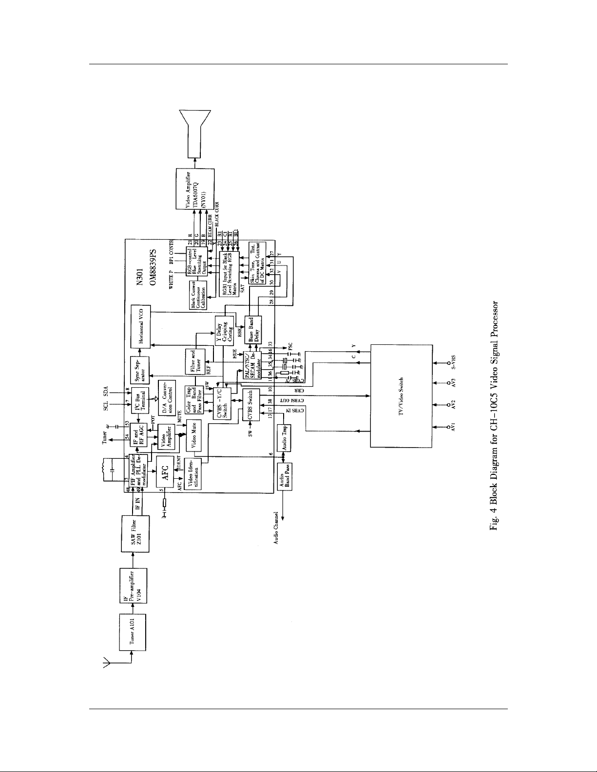
Block Diagram for Video Signal Processor ..................................................................7
SERVICE DATA .............................................................................................................................8
Technical Data of Key ICs ............................................................................................ 8
Service Data of Key ICs............................................................................................. 22
Waveforms of Key Points ........................................................................................... 28
ADJUSTMENTS............................................................................................................ 32
Set-up Adjustments.................................................................................................... 32
Circuit Adjustments .................................................................................................... 34
Service Mode and Bus Data ...................................................................................... 36
APPENDIX
1. Circuit Diagram
2. Final Wiring Diagram
3. Exploded View
4. Printed Circuit Board Diagrams
1

SERVICE MANUAL
SAFETY INSTRUCTIONS AND MAINTENANCE
WARNING: BEFORE SERVICING THIS CHASSIS, READ THE X-RAY RADIATION PRECAUTION ,
SAFETY PRECAUTION AND PRODUCT SAFETY NOTICE INSTRUCTIONS-BELOW.
X-RAY RADIATION PRECAUTION
1. The EHT must be checked every time the receiver is serviced to ensure that the CRT does not emit
X-ray radiation as result of excessive EHT voltage. The nominal EHT for this receiver is 29KV (for
25”TV) or 30KV (for 29”TV) at zero beam current (minimum brightness) operating at AC 120V. The
maximum EHT voltage permissible in any operating circumstances must not exceed 32KV (for
25”TV) or 33KV (for 29”TV). When checking the EHT, use the High Voltage Check procedure in this
manual using an accurate EHT voltmeter.
2. The only source of X-RAY radiation in this receiver is the CRT. To prevent X-ray radiation, the
replacement CRT must be identical to the original fitted as specified in the Parts List.
3. Some components used in this receiver have safety related characteristics preventing the CRT
from emitting X-ray radiation. For continued safety, replacement component should be made after
referring the PRODUCT SAFETY NOTICE below.
SAFETY PRECAUTION
1. The receiver has a nominal working EHT voltage of 29KV (for 25”TV) or 30KV (for 29”TV). Extreme
caution should be exercised when working on the receiver with the back removed.
1)
Do not attempt to service this receiver if you are not conversant with the precautions and procedures
for working on high voltage equipment.
2) When handling or working on the CRT, always discharge the anode to the receiver chassis before
removing the anode cap in case of electric shock.
3) The CRT, if broken, will violently expel glass fragments. Use shatterproof goggles and take extreme
care while handling.
4) Do not hold the CRT by the neck as this is a very dangerous practice.
2. It is essential that to maintain the safety of the customer all power cord forms be replaced exactly
as supplied from factory.
3. Voltage exists between the hot and cold ground when the TV is in operation. Install a separation
transformer during repairing or connecting to any testing equipment for the sake of safety. The
power of the separation transformer should exceed the rated overall power.
4. Replace blown fuses within the receiver with the fuse specified in the parts list.
5. When replacing wires or components to terminals or tags, wind the leads around the terminal
before soldering. When replacing safety components identified by the international hazard symbols
on the circuit diagram and parts list, it must be the company-approved type and must be mounted
as the original.
6. Keep wires away from high temperature components.
1

SERVICE MANUAL
PRODUCT SAFETY NOTICE
Many electrical and mechanical components in this chassis have special safety-related characteristics.
These characteristics are often passed unnoticed by a visual inspection and the X-ray radiation
protection afforded by them cannot necessarily be obtained by using replacements rated at higher
voltages or wattage, etc. Components which have these special safety characteristics in this manual
and its supplements are identified by the international hazard symbols in the circuit diagram and parts
list. Before replacing any of these components read the parts list in this manual carefully. Substitute
replacement components which do not have the same safety characteristics as specified in the parts
list may create X-ray radiation.
Safety Symbol Description
The lightning symbol in the triangle tells you that the voltage inside this product may be
strong enough to cause an electric shock. Extreme caution should be exercised when
working on the TV with the back removed.
This is an international hazard symbol, telling you that the components identified by the
symbol have special safety-related characteristics.
FDA This symbol tells you that the critical components identified by the FDA marking have
special safety-related characteristics.
UL This symbol tells you that the critical components identified by the UL marking have special
safety-related characteristics.
VDE This symbol tells you that the critical components identified by the VDE marking have
special safety-related characteristics
.
Maintenance
1. Place the TV set on a stable stand or base that is of adequate size and strength to prevent it from
being accidentally tipped over, pushed off, or pulled off. Do not place the set near or over a radiator
or heat register, or where it is exposed to direct sunlight.
2. Do not install the TV set in a place exposed to rain, water, excessive dust, mechanical vibrations or
impacts.
3. Allow enough space (at least 10cm) between the TV and wall or enclosures for proper ventilation.
4. Slots and openings in the cabinet should never be blocked by clothes or other objects.
5. Please power off the TV set and disconnect it from the wall immediately if any abnormal condition
are met, such as bad smell, belching smoke, sparkling, abnormal sound, no picture/sound/raster.
Hold the plug firmly when disconnecting the power cord.
6. Unplug the TV set from the wall outlet before cleaning or polishing it. Use a dry soft cloth for
cleaning the exterior of the TV set or CRT screen. Do not use liquid cleaners or aerosol cleaners.
2
SERVICE MANUAL
KEY ICS AND ASSEMBLIES
Table 1 Key ICs and Assemblies
Serial No. Position No. Model No. Function Description
1 N301 OM8839PS Small signal processor
2 N401 TDA8350Q Vertical output circuit
3 N852 LM317T Tri-terminal regulator
4 N601 TDA7057AQ Sound power amplifier
5 N001 LC86F3264AU-DIP Microcontroller
6 N002 AT24C04/AT24C08 EEPROM
7 NY01 TDA6107Q Video amplifier
8 DS01 HEF4053 Analog switch circuit
9 DS02 HEF4053 Analog switch circuit
10 N606 TDA9859 Audio processor
11 A101 TDQ-6F2M Tuner
Notes: AT24C04 (N002) is for MCR61TF30 only;
AT24C08 (N002) is for MCR66R400/MCR68R420/MCR68R800.
3
SERVICE MANUAL
BLOCK DIAGRAMS FOR CHASSIS
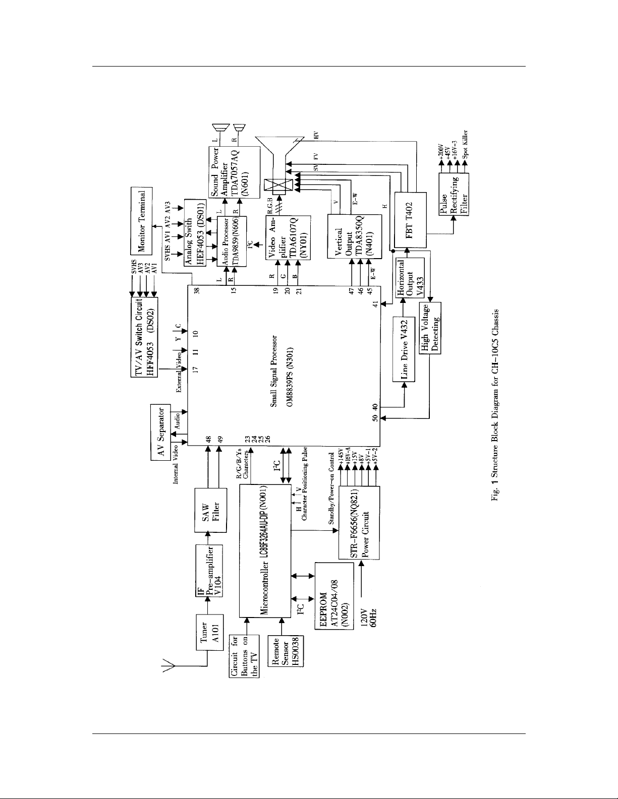
Structure Block Diagram
4
SERVICE MANUAL
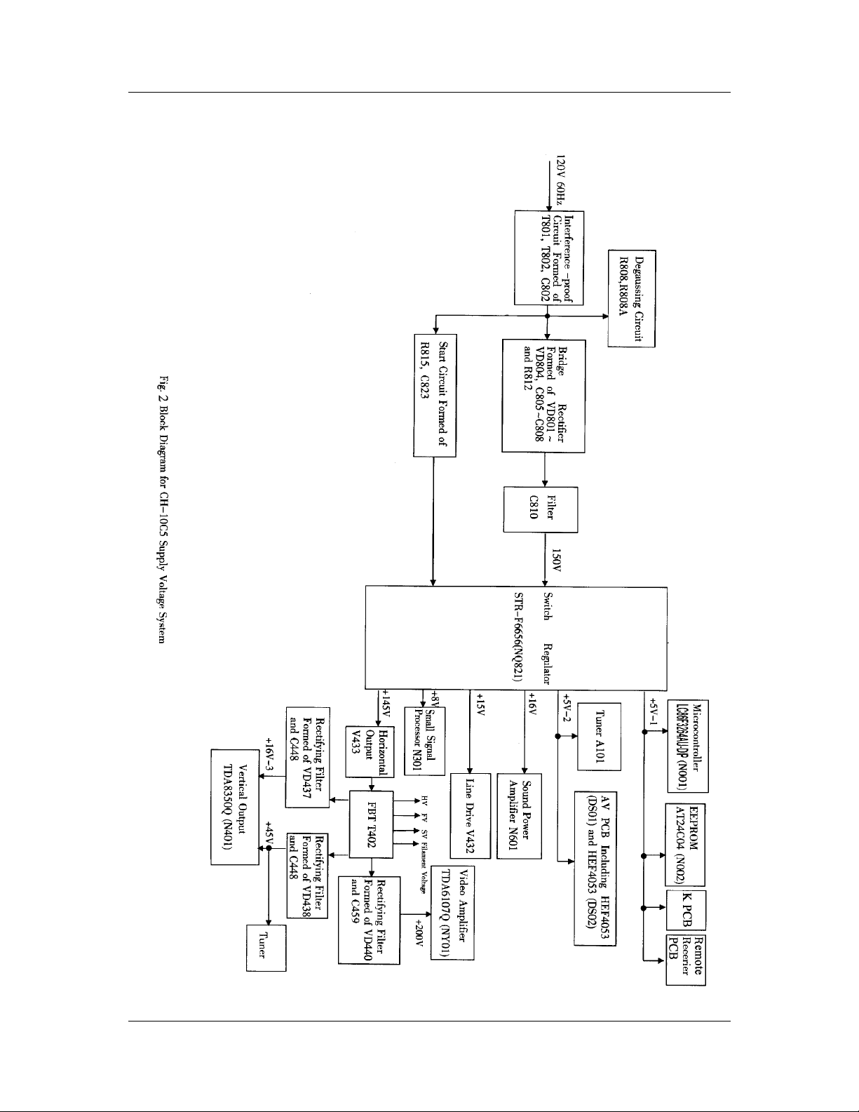
Block Diagram for Supply Voltage System
Fig.2 Block Diagram for CH-10C1(S) Supply Voltage System
5
SERVICE MANUAL
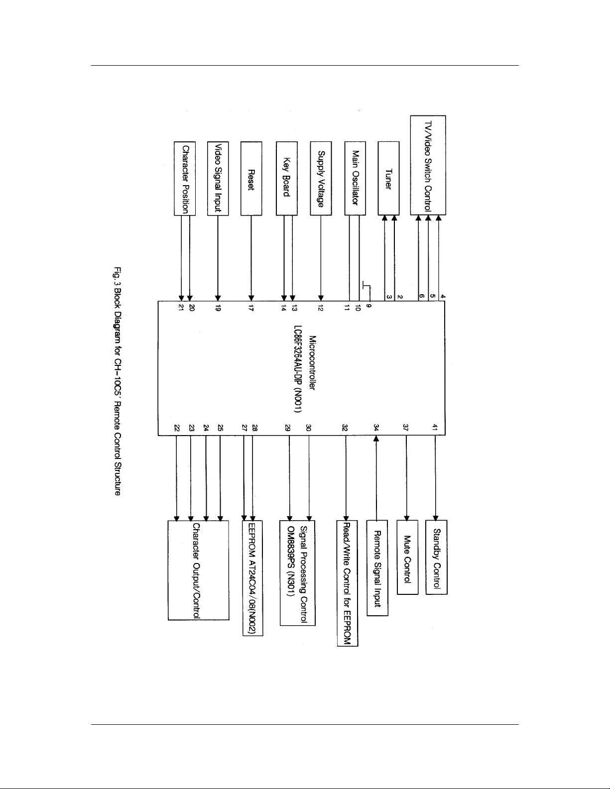
Black Diagram for Remote Control Structure
6
SERVICE MANUAL
Block Diagram for Video Signal Processor
7
SERVICE DATA
Technical Data of Key ICs
LC86F3264AU-DIP (N001)
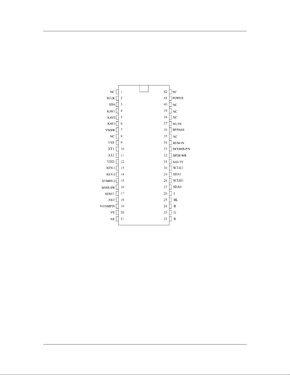
1. Terminal Assignment Layouts
SERVICE MANUAL
Fig. 5 LC86F3264AU-DIP DIP42S Terminal Assignment Layout
8
SERVICE MANUAL
2. Terminal Function
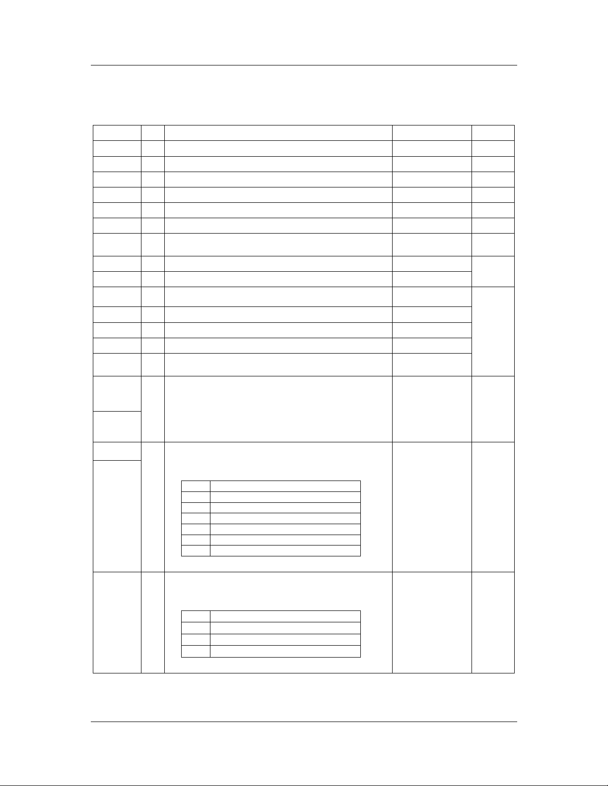
Table 2 Terminal Function Table
Terminal I/O Function Description Option Format
VSS - Negative power supply
XT1 1 Input terminal for crystal oscillation
XT2 O Output terminal for crystal oscillation
VDD - Positive power supply
RES I Reset terminal A
FILT O Charge-pump output terminal N
CVIN I
VS I
HS I
RO
GO
B O Blue (B) output terminal of RGB imagee
I O Intensity (I) output terminal of RGB image
RL O
Part 0
P00-P07
Port 1
P10-P17
Image signal input terminal
(available only in CH04T1002)
Vertical synchronization signal input terminal
Horizontal synchronization signal input terminal
Red (R) output terminal of RGB image
Green (R) output terminal of RGB image
Fast blanking control signal
Switch TV image and caption/OSD image signal
8-bit input/output port
Input/output can be specified in nibble unit
I/O
I/O
Other functions:
Hold release input
Internal input
8-bit input/output port
Each bit can be independently programmable
Other functions:
P10 SIO0 data output
P11 SIO0 data input/bus input/output
P12 SIO0 clock input/output
P13 PWM1 output
P14 PWM2 output
P15 PWM3 output
P17 Timer 1(PWM) output
Pull-up resistor
provided/not
provided
Output format
CMOS/Nch-OD
Output format
CMOS/Nch-OD
M
A
O
E
F
Port 6 I/O
4-bit input/output port
Each bit can be independently programmable
Other functions:
P60 IIC0 data input/output
P61 IIC0 clock output
P62 IIC1 data input/output
P63 IIC1 clock output
9

SERVICE MANUAL
Terminal I/O Function Description Option Format
4-bit input/output port
Port 7
I/O
P71-P73
Each bit can be independently programmable
Other functions:
INTO input/HOLD release input
P70
/Nch-Tr. output for watchdog timer
P71 INT1 input/HOLD release input
P72 INT2 input/timer 0 event input
INT3 input (noise rejection filter attached
P73
input)/timer 0 event input
Interrupt receiver format vector address
INTO
INT1
INT2
INT3
Rising Falling
yes
yes
yes
yes
yes
yes
yes
yes
Rising
/
Falling
no
no
yes
yes
H
levelLlevel
yes
yes
no
no
yes
yes
no
no
Vector
03H
0BH
13H
1BH
P70
W
P71-P73
V
Port 8
P83
P84-P87
Port options can be specified independently for each bit.
The programmable pull-up resistors are provided depending on whether CMOS or Nch-OD (Nch open
drain ) is selected as the port 1 option.
3. Refer to Table 3 about Functions and Data of the IC’s Each Pin.
I/O
1-bit input port
(P83 is set only in CH04T1002)
I
4-bit input/output port(P84-P87)
Each bit can be independently programmable
Other function:
AD converter input port
P83
B
P84-P87
X
10
SERVICE MANUAL
EEPROM AT24C04 (N002)
1. Features
Data EEPROM internally organized as 512
bytes and 32 pages×16 bytes
Low power CMOS
Vcc=2.7 to 5.5V operation
Two wire serial interface bus I
compatible
Filtered inputs for noise suppression with
Schmitt trigger
Clock frequency up to 400 kHz
High programming flexibility
-Internal programming voltage
-Self timed programming cycle including erase
-Byte-write and page-write programming
between 1 and 16 bytes
-Typical programming time 6 ms(<10ms) for up
to 16 bytes
High reliability
-Endurance 10
-Data retention 40 years
6
cycles
1)
1)
-ESD protection 4000 V on all pins
8 pin DIP/DSO packages
Available for extended temperature ranges
-Industrial -40 to +85
-Automotive -40 to +125
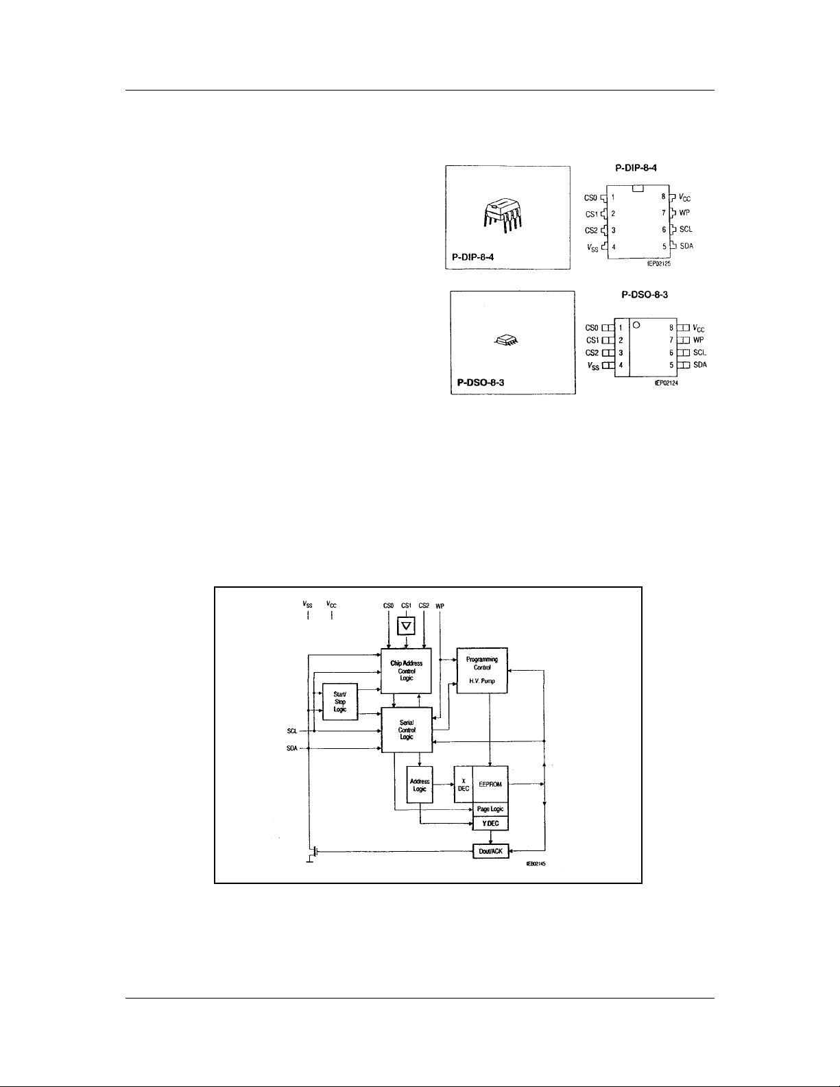
3. Block Diagram
2
C-Bus
2. Pin Configuration
Fig. 6
Fig. 7
4. Refer to Table 4 about Functions and Data of the IC’s Each Pin
11

SERVICE MANUAL
OM8839PS (N301)
I2C-bus Controlled PAL/NTSC/SECAM TV Processors
1. Features
The following features are available in all IC’s:
·Multi-standard vision IF circuit with an
alignment-free PLL demodulator without external
components
·Alignment-free multi-standard FM sound
demodulator (4.5 MHz to 6.5 MHz)
·Audio switch
·Flexible source selection with CVBS switch and
Y(CVBS)/C input so that a comb filter can be
applied
·Integrated chrominance trap circuit
·Integrated luminance delay line
·Asymmetrical peaking in the luminance channel
with a (defeatable) noise coring function
·Black stretching of non-standard CVBS or lumina-
nce signals
·Integrated chroma band-pass filter with switchable
centre frequency
·Dynamic skin tone control circuit
·Blue stretch circuit which offsets colours near
white towards blue
·RGB control circuit with “Continuous Cathode
Calibration” and white point adjustment
·Possibility to insert a“blue back” option when no
video signal is available
·Horizontal synchronization with two control loops
and alignment-free horizontal oscillator
·Vertical count-down circuit
·Vertical driver optimised for DC-coupled vertical
output stages
2
·I
C-bus control of various functions
2. General Description
The various versions of the TDA 884X/5X
series are I
2
processors which are intended to be applied in
PAL, NTSC, PAL/NTSC and multi-standard
television receivers. The N2 version is pin and
application compatible with the N1 version,
however, a new feature has been added which
makes the N2 more attractive. The IF PLL
demodulator has been replaced by an
alignment-free IF PLL demodulator with
internal VCO (no tuned circuit required). The
setting of the various frequencies (33.4, 33.9,
38, 38.9, 45.75 and 58.75 MHz) can be made
via the I
2
C-bus.
Because of this difference the N2 version is
compatible with the N1, however, N1 devices
cannot be used in an optimised N2 application.
Functionally the IC series is split up in 3
categories, viz:
·Versions intended to be used in economy TV
receivers with all basic functions (envelope:
S-DIP 56 and QFP 64)
·Versions with additional features like E-W
geometry control, H-V zoom function and
YUV interface which are intended for TV
receivers with 110° picture tubes (envelope:
S-DIP 56)
·Versions which have in addition a second
RGB input with saturation control and a
second CVBS output (envelope: QFP 64)
The various type numbers are given in the
table below.
C-bus controlled single chip TV
3. Survey of IC Types
Envelope S-DIP 56 QFP 64
TV receiver category Economy Mid/High end Economy Mid/High end
PAL only TDA 8840 TDA 8840H
PAL/NTS TDA 8841 TDA 8843 TDA 8841H
PAL/SECAM/NTSC TDA 8842 TDA 8844 TDA 8842H TDA 8854H
NTSC only TDA 8846/46A TDA 8847 TDA 8857H
12
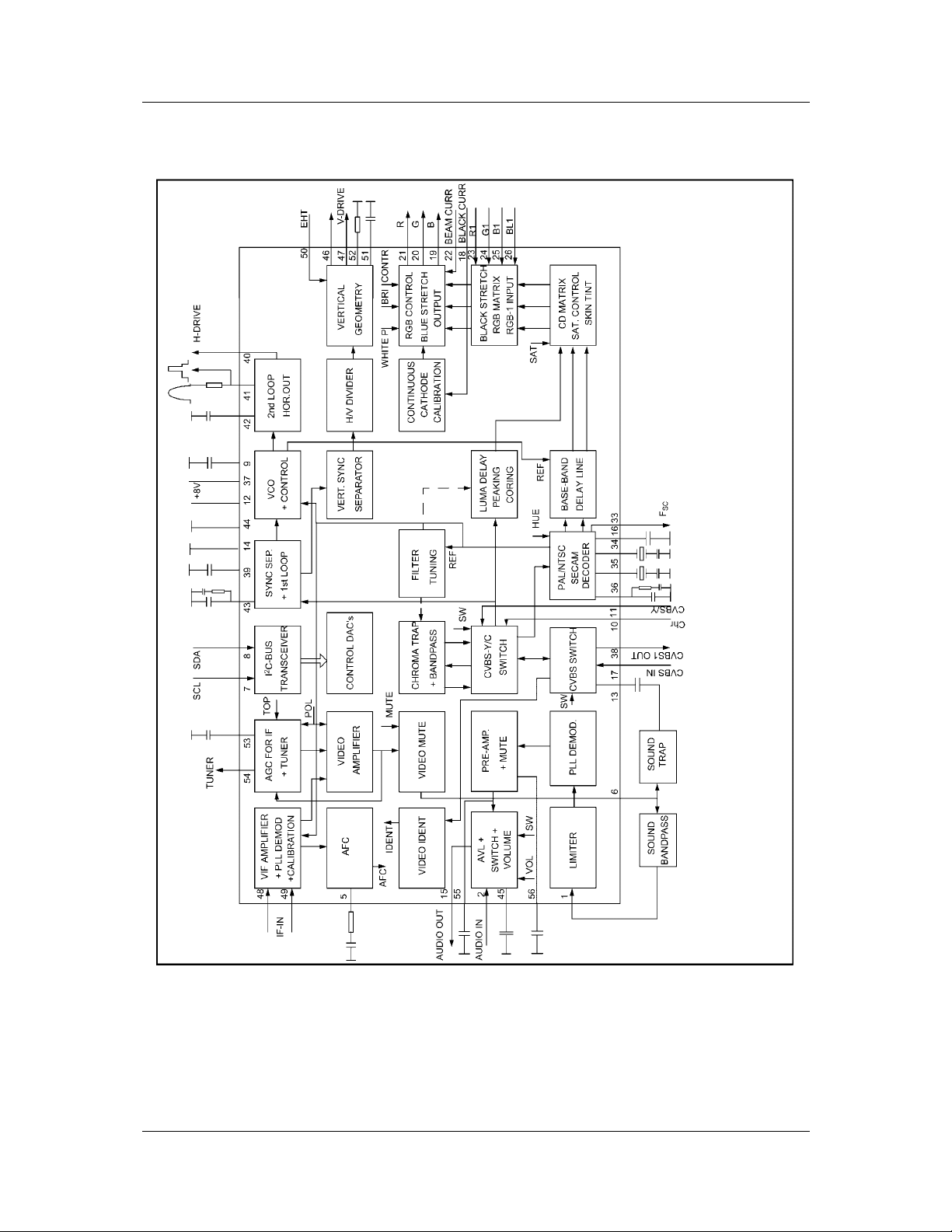
4. Block Diagram
SERVICE MANUAL
5. Refer to Table 5 about Functions and Data of the IC’s Each Pin.
13
Fig .8 Block Diagram “Economy Versions” (S-DIP 56 Envelope)
 Loading...