

Page 1

A-PDF MERGER DEMO
Page 2
Page 3
Page 4
Page 5
Page 6
Page 7
Page 8
Page 9
Page 10

Page 11

Page 12

Page 13

Page 14

Page 15

Page 16

Page 17

Page 18

Page 19

Page 20

Page 21

FP01
5A
120VAC
DP06
47V
RP06
LP02
To DeGauss
Circuit
RP05
DP22
TP22
RP28
TP23
RP25
RP30
2
DP01
4
3
CP24
1
RP27
RP23
RP21
RP31
DP26
CP23
Raw B+
156VDC
TP08
CP08
TP20
RP38
DP40
RP20
HOT COLD
LP03
3
8
9
5
16
14
15
13
10
11
12
DP80
CP80
NC
DP63
DP75
Reg B+UB
+33VE
DP85
+16VE
CP64
-12VE
CP76
DP31
DP30
16V
RP531
COLD
HOT COLD
IP01
13
3
2
2
1
RP54
4
HOT
IP50
Shunt
Reg
RP52
RP555
CP550
RP559
RP558
RP56
RP553
DP57
TP552
RegB+UB
Scan
Supply
RP53
TP553
RP556
ATC113 Power Supply
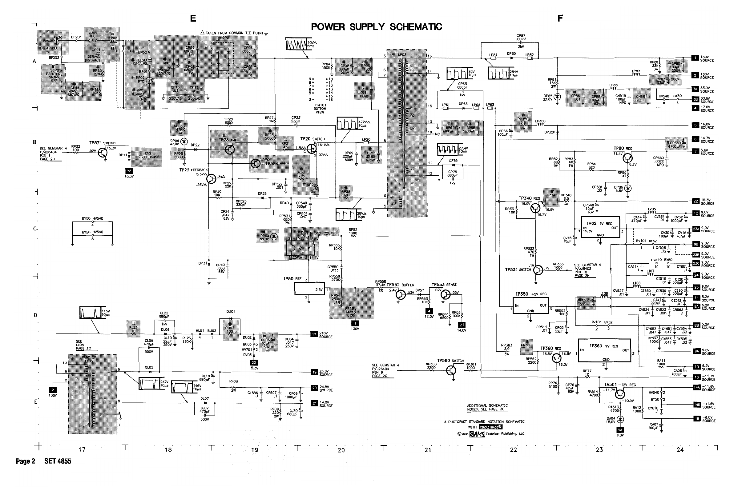
The standby supply is a high power, ZVS (Zero Voltage Switching) supply that minimizes
switching losses and radiated noise. ZVS refers to the ability of the supply causing the
voltage across the principal power output device, to reduce to near zero before the device
is switched on. Yet it has a slow enough time lag to allow the device to switch off
completely before any appreciable voltage is present across the device.
The MOSFET (TP20) begins conducting current when the gate voltage reaches the proper
turn on point. From that time, output current rises linearly due to the inductance of the
output transformer. However, once the gate voltage goes high, the drain voltage decreases
Page 9
Page 22

almost to zero volts. This eliminates much of the heat dissipation normally required of an
output device.
By reducing the switching losses to almost zero, the efficiency of the power supply is
greatly increased and the limiting of the switching voltages causes a substantial reduction
of switching noise.
Power Supply Operation
When AC is applied, DP01 converts the AC to approximately 156Vdc that is filtered by
CP08.
This “Raw B+” has two paths. First is through the transformer LP03 to the drain of TP20.
Second is through a series of resistors (RP27, 23, and 21) to the gate of TP20. As you
might guess this path is the start voltage for TP20.
With both drain and gate voltage TP20 conducts pulling the drain voltage to near zero,
collapsing the energy stored in LP03 winding pins 3, 8. This collapse causes voltage to be
induced into the secondary windings of LP03.
The winding on LP03 pins 9 and 5 is the secondary winding used for TP20 gate drive and
bias for TP22 and TP23. The pulse from this winding is sent to the anode and cathode of
DP26 and DP40 respectively. The positive bias is for the oscillator control circuit of TP22
and TP23. The negative bias is for IP01 and regulation. The un-rectified pulse provides
initial gate drive of TP20 via RP38, CP23, RP23, and RP21.
Oscillation occurs as TP20 turns on and off. TP22 and TP23 function as a latch circuit to
turn off TP20. As TP20 conducts, current is pulled through RP20. At some point the voltage
across RP20 increases till TP22 turns on. TP22 turns on pulling the base of TP23 lower
turning on TP23. With TP23 on, TP20 is turned off removing the voltage developed across
RP20 turning off TP22 and so on. The re-supply pulse and B+ through RP27 start the cycle
all over again.
Feedback is used to control the on time of TP20. The longer TP20 stays on, the more
current is developed in LP03. There are two feedback paths from the secondary side, the
+16V and the REG B+. Both voltages are required for proper regulation and run of the
power supply. IP50 shunt regulator controls the voltage across IP01 pins 1 and 2. As Reg
B+ goes up, IP50 becomes more resistive or open turning off IP01.
IP01 is used to couple the secondary to the primary. As the transistor in IP01 turns on
more, the less negative pin 4 becomes. This causes DP20’s emitter voltage to be more
positive. A more positive voltage on the emitter of TP22 means that the base voltage needs
to be more positive for it to turn on, there for TP20 stays on longer.
Page 10
Page 23

FP01
5A
120VAC
DP06
47V
RP06
LP02
To DeGauss
Circuit
RP05
DP22
TP22
21
RP28
TP23
RP25
RP30
DP01
4
3
CP24
RP27
RP23
RP21
RP31
DP26
CP23
Raw B+
156VDC
TP08
CP08
TP20
RP38
DP40
RP20
HOT COLD
LP03
3
8
9
5
16
14
15
13
10
11
12
DP80
CP80
NC
DP63
DP75
Reg B+UB
+33VE
DP85
+16VE
CP64
-12VE
CP76
HOT COLD
1
2
3
1
2
RP54
RP52
RP555
CP550
RP559
RP558
RP56
DP31
DP30
16V
RP531
IP01
3
4
HOT
COLD
IP50
Shunt
Reg
Key points about the ATC113 ZVS power supply:
• Stand-by operating frequency of 60 to 65KHz.
• RP20 over current protection.
• DP30 over voltage protection.
• TP552 and TP553 used for run mode current increase.
• If TP20 fails replace all active components on primary side.
• Run operating frequency of 40 to 50KHz.
Scan
Supply
RP553
RP53
DP57
TP553
RP556
TP552
RegB+UB
Page 11
Page 24

Power Supply Troubleshooting Tips
NOTE: Voltage readings taken at 90VAC input using a Vari-AC.
Regulation Problem:
IP01 (Photo-Coupler) can be by-passed by shorting pins 1 and 2 of IP01, and connecting a
10K potentiometer across pins 3 and 4. With the potentiometer set to 10K the Reg B+ is
aprox. +140Vdc. At 7.5K the Reg B+ was aprox. +100Vdc.
IP50 can also be checked with the same setup as in IP01. As the Reg B+ goes up IP50
conducts. Monitoring pin 3 of IP50 and with Reg B+ at +100Vdc pin 3 is aporx. +12.5Vdc.
As Reg B+ goes up IP50 will conduct and pin 3 will drop to +1.8Vdc. By using the 10K
potentiometer one can vary the Reg B+ and check all functions of feedback control.
Start-up Problem:
Unsolder the Drain of TP20 and turn on the Vari-AC. The gate voltage of TP20 should
measure +11.5Vdc. Anything less check for loads in the star-up circuit. Anything more
check for an open in OSC circuit and DP06 circuit.
Check for shorts on the secondary of LP03. Excessive load on the power supply will cause
it to shutdown and pulse.
Page 12
Page 25

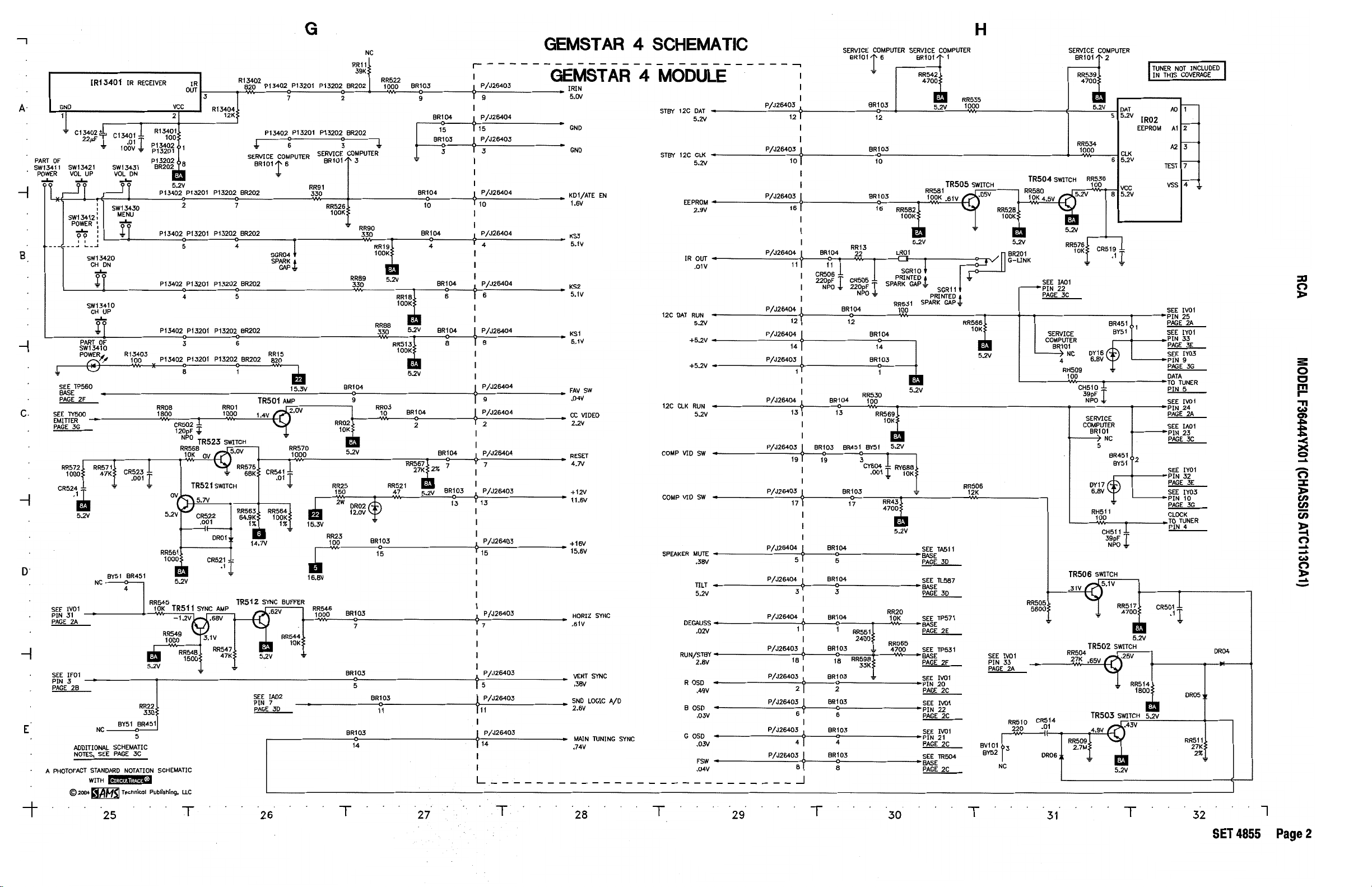
+5.2VE4
Gemstar 4
U26401
TR504
TR505
J26404
J26403
EEPROM Enable
8
5
IR02
6
4
Clock
I2C Stby
Data
BR103 BR104
ChipperCheck
Service Connector
BR101
BR202
Keyboard
1
1 2 3 4 5 6 7 8 9 10 11 12 13 14 151 2 3 4 5 6 7 8 9 10 11 12 13 14 15 16 17 18 19
to
IR
2
4
5
6
7
KS3
KS2
KS1
KD1
2
I
C Run
Data
Clock
+5.2VE
IR Out
ECO
Gemstar 4 and System Control
The Gemstar module is used to generate the electronic program guide (EPG) and control
the chassis. The main processing IC, for the EPG, is U26401. U26401 has two main
functions; in standby U26401 processes information for the EPG and user input, in the run
mode U26401 controls the different functions of the chassis. The two flat ribbon cables
that connect the Gem4 module to the chassis are BR103 and BR104.
Power for the module comes from the +5.2VE via pin 14 of BR104. The standby I2C bus
provides communications to the EEPROM (IR02) and the Chipper Check interface via
BR103 pins 10 and 12. The Run I2C bus on pins 12 and 13 of BR104 provide
communication to the tuner, video processing (IV01), video switching and audio processing
(IA01) and switching IC’s. PIP functions are also controlled by the run clock and data.
User input is via remote or keyboard. BR103 pin 9 is the IR input to the Gem4 module and
keyboard input is on pins 4, 6, 8, and 10 of BR104. These signals are processed by the
system control and commands are sent to the chassis via I2C bus on BR104 pins 12 and
13.
Page 6
Page 26

Troubleshooting the Gem4
1. With AC power applied to the set.
2. Check BR104-14 for +5.2VE
3. Voltage incorrect or missing, troubleshoot STBY power supply
4. Check BR103-10 and 12 (Clock & Data) for +5.0Vdc and 5Vp-p signal.
5. Signal present all the time troubleshoot main chassis and IR02.
6. Check BR104-4, 6, 8, and 10 for proper DC levels. Incorrect DC levels disconnect
BR202 and recheck.
7. Correct DC levels with BR202 disconnected troubleshoot keyboard.
8. Check for signal at BR104-12 and 13 when power button is pressed.
9. Clock and Data signal present when power is pressed troubleshoot the chassis.
10. Not present replace Gemstar module.
Start-up and Shutdown
3 Strikes and You’re Out Shutdown
The below error code table shows the different codes that can be thrown during the 3
strikes shutdown. The error codes can be viewed by accessing the service menu. Parameters 1, 2, and 3 are reserved for error codes. When viewing error codes for the first time it
is a good idea to reset all to zero and let the set go through the 3 strikes again. The new
error codes will indicate the first problem detected by the system control during start-up.
Error Code
(Dec)
00 No error code thrown
03 U26401 Gemstar Micro 12V Run fault
08
09
11
12
16
18
44
176
180
IV01 XRP event detected
IV01 Power on reset
IY03 F2PIP Power on reset
IA01 Stereo Decoder Power on reset
U26401 Gemstar Micro Run I2C clock or data clamped at logic state 0
U26401 Gemstar Micro Stand-by I2C clock or data clamped at logic state 0
IY03 F2PIP No acknowledge from device
IA01 Stereo Decoder No acknowledge from device
3-Line Comb No acknowledge from device
Device Condition
144
194
IY01 A/V Switch No acknowledge from device
Tuner No acknowledge from device
Page 7
Page 27

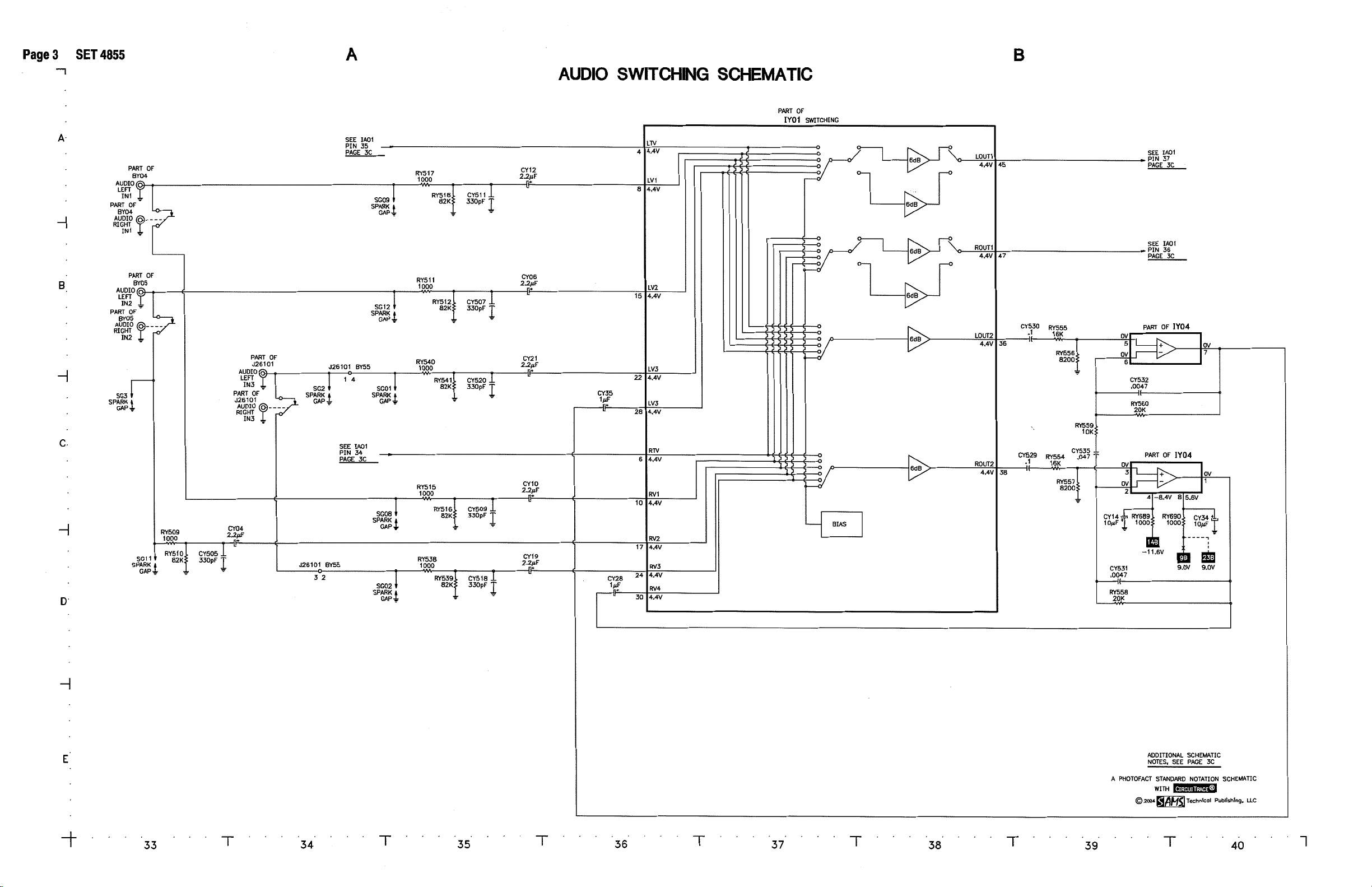
Y
Pr
Pb
XBox
Connector
BY51
XBox SW
3
1
BIAS
6
4
GND
5
BIAS
6
4
GND
5
VCC
Buffer
OUT
2
IY09
3
1
VCC
Buffer
OUT
2
IY07
3233
ClockData
16
Yin
IY01
Vcc
Yout
1
+5VE
Pb
BV101
40 +9VE
Pr
Pr
Pb
Y
Y
Chassis
CRT Board
R
14
G
15
IV01
43
16
44
47
IU01
B
BY52
7 41
I/O Board
Chassis
3
1
BIAS
6
4
GND
5
Buffer
VCC
IY08
OUT
2
IY03 PIP
BY50
ATC113 Y Pr Pb Path
The ATC113 is capable of two YPrPb inputs via conventional YPrPb cable and a special
cable connected to the V-Port (X-Box). Both inputs go three switch IC’s, IY09 for the Y
signal, IY07 for the Pr signal, and IY08 for the Pb signal. A voltage from the Gemstar
system control switches the three IC’s. BY51 pin 3 (XBOX SW) goes high approximately
3.1Vdc when the user selects V-Port input. When low, component input is selected. The Y
signal is further switched by IY01 (Audio / Video switch IC) and sent to the PIP processor or
comb filter. After PIP / Comb processing the Y signal along with Pr and Pb signals are sent
to connector BV101 and to the main chassis. All three signals are further processed by
IV01 and output as RGB to the CRT driver IU01.
I/O Module Troubleshooting
NOTE: Without the I/O module connected to the chassis the set will go through the 3-
strikes and you’re out shutdown.
The different I/O modules are board level troubleshooting. By checking the signals and
voltages to and from the I/O one can isolate down to board level. There are no set
procedures for this type of troubleshooting. Checking all signals and voltages on all
connectors is the only way to troubleshoot the I/O module. See service data for signal and
voltage requirements of each I/O.
Page 8
 Loading...