

Page 1
TO
E8
RED BIAS
VERTICAL
<21-B>
TO
E7
GRN BIAS
E5003
E5007
TP50
RED OUTPUT
194V
FOREWORD
This publication is intended to aid the technician in servicing the CTC195/197 television
chassis. It will explain the theory of operation, highlighting new and different circuits
associated with the digitally controlled chassis. The manual covers power supply,
horizontal and vertical deflection, video signal processing, and audio signal processing
theory of operation along with practical, proven troubleshooting methods. It is designed
to assist the technician to become more familiar with the chassis operation, increase
confidence and improve overall efficiency in servicing the product.
Note: This publication is intended to be used only as a training aid. It is not meant to
replace service data. Thomson Consumer Electronics Service Data for these instruments
contains specific information about parts, safety and alignment procedures and must be
consulted before performing any service. The information in this manual is as accurate
as possible at the time of publication. Circuit designs and drawings are subject to change
without notice.
SAFETY INFORMATION CAUTION
Safety information is contained in the appropriate Thomson Consumer Electronics Service
Data. All product safety requirements must be complied with prior to returning the
instrument to the consumer. Servicers who defeat safety features or fail to perform safety
checks may be liable for any resulting damages and may expose themselves and others to
possible injury.
All integrated circuits, all surface mounted devices, and many other
semiconductors are electrostatically sensitive and therefore require
special handling techniques.
Chipper Check® is a registered trademark of Thomson Consumer Electronics.
dbx® is a registered trademark of Carillon Electronics Corporation.
DSS® is a registered trademark of DirecTV, Inc., a unit of Hughes Electronics Corp.
TV Guide Plus+® is a registered trademark of Gemstar Development Corporation.
TV Guide® is a registered trademark of TV Guide Financial, Inc.
SRS®, the SRS symbol and Sound Retrieval System® are registered trademarks of
SRS Labs, Inc.
First Edition 9726 - First Printing
Copyright 1997 Thomson Consumer Electronics, Inc.
Trademark(s)® Registered Marca(s) Registrada(s)
Printed in U.S.A.
Prepared by
Thomson Consumer Electronics, Inc.
Technical Training Department
PO Box 1976
Indianapolis, Indiana 46206 U.S.A.
®
Page 2

Contents
General Features: ...............................................................................................................6
Technical Overview .......................................................................................................... 12
CTC195/197 “Main” Power Supply .............................................................................. 15
AC In and Degaussing ..........................................................................................................................15
Power Supply Operation .......................................................................................................................16
Secondary Supply Operation ................................................................................................................19
Troubleshooting ................................................................................................................ .................... 20
Auxiliary Power Supply Operation ............................................................................... 2 2
CTC195 Convergence Power Supply Overview ........................................................... 2 5
Power Supply Operation .......................................................................................................................26
Horizontal Deflection Overview..................................................................................... 30
Horizontal Circuits .......................................................................................................... 32
AFC and APC .......................................................................................................................................32
Horizontal Driver ..................................................................................................................................33
Horizontal Output .................................................................................................................................33
E/W Pin Correction & S-Correction (CTC197) ................................................................................... 35
E/W Pin Correction & S-Correction (CTC195) ................................................................................... 35
X-Ray Protection Circuit ......................................................................................................................36
Z-Axis Correction ................................................................................................................................. 37
Troubleshooting ................................................................................................................ .................... 38
Vertical Circuits................................................................................................................ 40
Half-Supply ........................................................................................................................................... 41
Troubleshooting ................................................................................................................ .................... 45
No Vertical Deflection .......................................................................................................................... 45
Scan Loss Detect & Shutdown Overview ............................................................................................46
Scan Loss Detect Operation.................................................................................................................. 47
System Control ................................................................................................................. 50
Overview ............................................................................................................................................... 50
Standby/AC Line Dropout Detector and Reset .................................................................................... 52
Reset, Recovery, Initialization and BrownOut ....................................................................................52
Software detection ................................................................................................................................ 52
+16V Standby........................................................................................................................................ 52
15 Second Timer ...................................................................................................................................53
POR ( Power Off Reset) .......................................................................................................................53
EEPROM and T4 Chip Power Control ............................................................................................... .54
Main Power Supply On/Off Control.....................................................................................................54
Power Down..........................................................................................................................................56
Batten Down the Hatches .....................................................................................................................56
Feature Auto Detection .........................................................................................................................58
Run Supply Detector............................................................................................................................. 58
Microprocessor Input Signals ...............................................................................................................59
Microprocessor Pin Assignments .........................................................................................................59
U13101 Pin Functions: .........................................................................................................................60
Page 3

IR Input.................................................................................................................................................. 66
OSD Circuit.......................................................................................................................................... 66
Service Menu ........................................................................................................................................67
Error Codes ...........................................................................................................................................68
Troubleshooting ................................................................................................................ .................... 70
I²C Bus................................................................................................................................................... 70
Main Tuner ....................................................................................................................... 7 5
Input Splitter.......................................................................................................................................... 76
Single Tuned Input Filtering................................................................................................................. 76
RF Amplifier .........................................................................................................................................76
RF Bandpass .......................................................................................................................................... 77
Mixer/Oscillator ....................................................................................................................................77
IF Bandpass ...........................................................................................................................................77
PLL / Frequency Synthesizer ................................................................................................................ 77
Bandswitching....................................................................................................................................... 78
Tuning ................................................................................................................................................... 78
Channel Selection .................................................................................................................................79
Software Control ................................................................................................................................... 80
EEPROM Requirements .......................................................................................................................81
IF Alignment ......................................................................................................................................... 81
IF DACS................................................................................................................................................81
Tuner Alignment ................................................................................................................................... 81
Troubleshooting ................................................................................................................ .................... 83
Electronic Alignment ............................................................................................................................ 83
RF Bandswitching.................................................................................................................................83
Channel Switching ................................................................................................................................85
No Tuning .............................................................................................................................................86
FPIP/2nd Tuner Overview .............................................................................................. 88
Video Input Switching .......................................................................................................................... 91
FPIP (U18100) Overview ..................................................................................................................... 92
FPIP Signal Switching .......................................................................................................................... 93
FPIP IC U18100 Pinout ........................................................................................................................ 96
Second Tuner (PIP) ............................................................................................................................... 98
PIP 2nd Tuner/IF.................................................................................................................................100
T4 Chip U16201.............................................................................................................. 101
T-Chip Overview ................................................................................................................................101
T4 Chip Bus Specifics ........................................................................................................................101
POR (Power-On Reset) Operation .....................................................................................................101
Bus Transceiver Reset.........................................................................................................................101
Transceiver Power Supply and Register Volatility............................................................................. 103
IF Processing .......................................................................................................................................103
Audio Detection ..................................................................................................................................103
CRT Management .............................................................................................................................. 103
Deflection Processing ......................................................................................................................... 103
Video Processing.................................................................................................................................103
Page 4

Video Processing ............................................................................................................. 104
Luma Processing .................................................................................................................................105
Chroma Processing ............................................................................................................................. 106
RGB Interface .....................................................................................................................................108
External RGB Input Processing..........................................................................................................108
RGB Output Section ...........................................................................................................................108
CRT Management ...............................................................................................................................109
Beam Current Limiting ....................................................................................................................... 109
CRT Drivers ........................................................................................................................................ 110
Automatic Kine Bias & Scan Velocity Modulation..................................................... 111
Scan Velocity Modulation................................................................................................................... 111
Automatic Kine Bias...........................................................................................................................112
AKB Operation ................................................................................................................................... 115
Start-up ................................................................................................................................................ 116
CTC195 AKB ..................................................................................................................................... 117
AKB and Color Temperature Alignment............................................................................................ 118
Audio Processing Overview .......................................................................................... 120
Audio Input/Switching Circuit............................................................................................................122
Balance Control ................................................................................................................................... 122
Volume Taper & Fletcher-Munson Network...................................................................................... 124
Audio Output Circuit ..........................................................................................................................125
AVR (Automatic Volume Reduction)................................................................................................ 127
SRS/Compressor Circuits.............................................................................................. 128
TV Guide Plus+ .............................................................................................................. 1 31
EPG Self-Diagnositcs ......................................................................................................................... 131
Menu’s ................................................................................................................................................. 132
Obtaining More Information...............................................................................................................132
Customizing The Channel Listing......................................................................................................132
One Touch Recording .........................................................................................................................132
Recording Options .............................................................................................................................. 132
Troubleshooting ................................................................................................................ .................. 132
Blank Screen .......................................................................................................................................132
No Sound, Picture Okay .....................................................................................................................133
Can’t Select Desired Channel .............................................................................................................133
Noisy Stereo Reception.......................................................................................................................133
No Picture, No Sound but TV is on.................................................................................................... 133
Sound Okay, Poor Picture ...................................................................................................................133
Black Box Appears on the Screen ......................................................................................................133
TV Guide Plus+ IR Controllers Not Working.................................................................................... 133
TV Guide Plus+ Cable Box Codes .....................................................................................................134
TV Guide Plus+ VCR Codes .............................................................................................................. 134
Page 5

PTV Digital Convergence Overview............................................................................ 13 6
Circuit Description..............................................................................................................................137
Digital Convergence Circuit ...............................................................................................................140
Convergence Yoke Drivers ....................................................................................................... .......... 142
Crosspoint Adjustments ......................................................................................................................144
Front Panel Service Mode..................................................................................................................145
Remote Control Service Functions............................................................................................... ...... 146
Convergence and Alignment Specifications ...................................................................................... 148
DigiCon Service .................................................................................................................................. 150
T-Chip Alignment ............................................................................................................................... 150
Banding ...............................................................................................................................................151
Digital Convergence Failure ...............................................................................................................152
CRT Replacement ...............................................................................................................................152
Digital Convergence IC ......................................................................................................................153
Convergence "Jumps" ......................................................................................................................... 153
Troubleshooting (General) .................................................................................................................. 154
Troubleshooting Geometry .................................................................................................................154
Troubleshooting Convergence............................................................................................................156
CRT Replacement ...............................................................................................................................156
EEPROM Replacement ...................................................................................................................... 161
Main EEPROM Replacement............................................................................................................. 161
DigiCon EEPROM Replacement ....................................................................................................... 161
DigiCon IC Replacement....................................................................................................................164
Red/Green/Blue CRT's........................................................................................................................ 165
Chipper Check Overview .............................................................................................. 166
Chipper Check Hardware.................................................................................................................... 167
Chipper Check Software .....................................................................................................................168
“Dead Set” Troubleshooting with Chipper Check ............................................................................. 169
Chipper Check Hookup ......................................................................................................................170
Chipper Check Operation ...................................................................................................................170
Diagnostic Function ............................................................................................................................170
Alignments Function ...........................................................................................................................171
Part Replaced Function ....................................................................................................................... 171
Page 6

6 Overview
General Features:
The CTC195/197 chassis is the latest in the Thomson Consumer Electronics line of
digitally controlled television receivers. It relies on microprocessor control to govern
the entire operation of the television, including consumer operation, system operation,
system monitoring and maintenance. The control circuits are not only responsible for
turning the set on and off, but also for aligning the different circuits such as deflection
and signal. Adjustments that were previously aligned with a potentiometer on other
chassis are now aligned digitally via the microprocessor with the values stored in the
EEPROM (Electrically Erasable Programmable Read Only Memory). The CTC197
will eventually replace a wide range of current TCE chassis', including the CTC169
and CTC176/177 series direct view chassis. Video and audio feature requirements
reflect a range of performance from previous core line products to midrange featured
sets. The basic feature package will include dBx stereo, 8 jack panel, and an on-screen
program guide.
Screen Sizes
The CTC197 covers direct view screen sizes from 27" to 35", measured diagonally.
The CTC195 will be used in PTV screen diagonal sizes from 46" to 61".
The projection television CTC195 chassis utilizes the CTC197 basic chassis plus
additional circuitry to adapt it for projection TV operation. The additional circuitry
consists of the "Digital Convergence" circuit board and it's own dedicated power
supply. The CTC195, unlike earlier PTV's that used analog convergence, uses the all
new "Digital Convergence" circuitry to provide near perfect convergence and linearity.
The CTC195 will replace previous PTV chassis CTC169, CTC178/188 and CTC187.
Video
The video performance of the CTC197 covers both low and mid levels. Models are
specified to include comb filter and S-VHS (where 600 LOR (Lines of Resolution) is
required) or non-comb filter without S-VHS (where 280 LOR is required). Auto
Color and AKB (Automatic Kine Bias) are basic for all chassis versions.
Tuning
CTC197 tuners incorporate the necessary specifications to follow normally accepted
cable TV tuning capabilities and will also meet the latest FCC "cable ready" requirments.
Channel tuning is also enhanced through a Fast Tune option.
Audio
CTC197 audio circuitry includes dBx stereo and is configured for both 1 watt and 5
watt output version. The CTC195 will add a 10 watt audio amplifier.
Page 7

The CTC197 contains a wide array of consumer selections and controls. Among them
are:
Sleep Timer
The sleep timer has four hour functionality and can be set in increments of fifteen
minutes. The OSD counts down time remaining when the sleep timer function is
enabled. The Sleep Time function also includes a descending audio taper automatically
implemented the last one minute of Sleep Timer operation.
On Screen Time and Channel Display
The On Screen Time and Channel features allows the current time and channel to be
displayed on screen. This feature can be programmed for continuous display through a
menu item (continuous display is not an option on PTV). This includes both AM and
PM selections. In cases where time has not been set, only the channel will be
displayed.
Factory Reset
Resets all consumer picture quality adjustments to one of three factory present conditions.
Auto Program
Overview 7
Automatically locates and enters into memory all active channels.
Commercial Skip
Commercial Skip is user implemented in thirty second increments up to four minutes
and then 60 second increments up to one hour. When CS times out, the programming
will return to the channel that was on screen when CS was initially entered. When CS
is enabled in two tuner PIP sets, the original channel will automatically appear in the
second tuner PIP. When CS times out, PIP is disabled.
Multilingual OSD
The CTC197 will support up to three customer-selectable OSD languages. Languages
will include: English, Spanish or Portuguese.
Alarm Timer
The Alarm Timer feature permits the user to set the TV to come on automatically at a
preset time every day. The TV will automatically turn off after two hours if no
other function is accessed by the consumer (i.e., volume, channel, etc.).
Parental Control
The parental control feature permits the user to engage a secondary scan list with more
limited channel choices. This may be used by parents to control the channel selection
capabilities of the set when they are not able to supervise program selection.
Page 8

8 Overview
Auto Tune (VCR/Cable/DSS Set-Up)
Auto select allows the user to select which channel or external input should automatically
be selected when the VCR1, VCR/LD or cable/DSS key is pressed on the remote.
Auto select set-up is accessible via on screen menu.
Channel Labeling
Channel labeling is permitted for no less than 28, four-character or 14, eight character
labels.
Channel Directory
The Channel Directory Feature permits up to 28 channels and their consumer input
labels to be displayed on-screen as an index. The channel directory presentation may
consist of more than one display screen.
TV Guide Plus+
Displays program title, length, elapsed time, program description, channel labeling and
EDS (Extended Data Service) broadcast early warning display in areas where the
system is broadcast. A menu item assisting in the selection of “Eastern Standard,
Central Western” standard time will be provided.
Closed Captioning
Field one and Field two of closed captioning are supported (CC1, CC2, CC3, CC4,
T1, T2, T3, T4). CCD enabling is through TV menu selection.
Color Temperature
A three position, user-selectable color temperature switch is available via the on screen
display system.
Interface
The CTC195/197 will support two levels of consumer feature operation. On select
chassis versions, the basic interface will be augmented with an ICON based "Fetch"
Menu. Highlighting and enabling a Fetch Icon automatically implements the set-up
menu of the feature or enables it. Fetch Menu items include: sleep timer, front panel
lockout, parental control, alarm timer, initial setup, and channel directory.
Mute
The Mute feature can be enabled via remote control or TV menu selection. Mute with
automatic CCD (Closed-Captioning) operation is consumer selectable via a menu
selection. When Mute and automatic CCD is selected the consumer CCD preference
will automatically be displayed. If no consumer preference has been noted, CC1 will
be selected. Text will not be permitted as an option.
Page 9

Front Panel Lock-Out
Front Panel Lock-Out disables the front TV access buttons. It can be enabled through
either the remote control or via menu option. Once enabled, the Front Panel
Lock-Out feature can be disabled through either remote command or by disconnecting
AC power to the set for more than sixty minutes.
Fast Track Tuning
The CTC197 will support, via the front panel or remote, a two speed tuning feature.
When the channel up/down key is depressed, the set will continuously select and tune
the next highest/lowest channel and displays it with OSD for 500 ms. If the channel up/
down key is held down for three or more seconds, the Fast Track Tuning feature is
enabled and the TV will select and tune the next highest/lowest channel at a more rapid
rate.
Cable Ready
Provides the channel capacity to provide the accepted “cable ready” standard.
FPIP
Overview 9
Basic Color PIP (FPIP) will be an optional feature on select chassis versions. PIP
features are similar to the CTC187 implementation including swap, and PIP continuous
move. Channel labeling will only be supported in the main picture. PIP can utilize Aux
1 (or S-VHS) as the second video source. Where a second source is not available,
both the big picture and small picture will be the same. Fast Track tuning is provided
for either small or large pix.
Two Tuner PIP
Two tuner PIP (T2FPIP) will be supported on select chassis versions. T2FPIP
features will be the same as those of FPIP but also include channel labeling of both
main and small PIP. Fast Track tuning is active for both small and large pix. The
CTC197 does not support separate main picture vs PIP color controls.
A/V Jack Panel
The jack panel will include two video inputs, one pair of left and right audio inputs and
an S-Video input jack. There will also be one pair of variable (hi-fi) left and right audio
outputs.
S-Video
Select CTC197 chassis will support S-Video with auto detection of the signal when
there is an active S-Video input. The S-Video input will replace Video Input 1.
Page 10
10 Overview
POWER
DVD
VCR1
VCR2
SAT
CABLE
AUDIO
TV
REVERSE
RECORD
INFO
VOL
MUTE
1
4
7
FAV INPUT
CLEAR
STOP
2
5
8
0
MENU
PLAY
CH+
CH-
SELECT
FORWARD
PAUSE
SKIP
VOL
GO BACK
3
6
9
ANTENNA
RESET
PIP
MOVE
SOUND
FETCH
CH CTRLSWAP
CRK70 Series Remote Control
Page 11

Comb Filter
A digital comb filter will be employed on select chassis versions. Comb filter versions
will also support consumer switchable video noise reduction.
No Signal Present
When the TV is placed in the S-Video or Video Input mode, and no signal is present, a
gray screen with the caption "No Signal Present" will be displayed.
dbx/SAP Audio
The CTC197 will support dbx/SAP. SAP (Separate Audio Programming) is a
selectable user feature that is specific to the channel selected. When Commercial Skip
is enabled while on a station broadcasting SAP programming, when the original channel
is retuned, SAP is re-enabled.
Audio Speaker Select
A menu option will permit the customer to turn internal speakers on or off.
Treble/Bass/Balance
Overview 11
The audio treble, bass and balance may be adjusted from the menu system.
SRS (Sound Retrieval System)
Basic SRS is supported via OSD. SRS audio is implemented through the internal
speakers. There is no external SRS speaker terminals.
Front Panel Controls
The front panel will provide Menu, Channel Up, Channel Down, Volume Up, Volume
Down and Power buttons.
Remote Use
The CTC197 uses the CRK70, CRK74, CRK83, & CRK84 remote controls.
Page 12

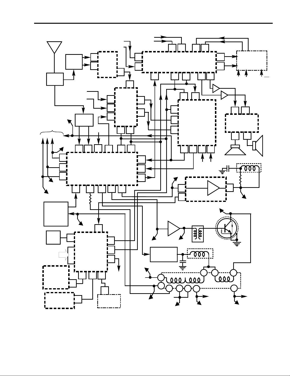
12 Overview
Technical Overview
The CTC197 was designed to provide a mid/high end replacement chassis for a broad
spectrum of TCE product line.
The CTC197 chassis begins with a bus controlled, tuner on board concept similar to
the CTC175/176/177 family and begins to expand on this base. The key developments
in the CTC197 are the T4 Chip, the FPIP IC, and a new Stereo IC.
The new T4 (U16201), used in part in the CTC185 chassis, allows more bus control of
adjustments and incorporates AKB (Automatic Kine Bias) and places the calculations
for AKB control with software.
The FPIP IC (U18100) is new to the CTC197 and allows bus control of PIP functions.
Although similar to the DPIP found in the CTC187, the FPIP also incorporates video
switching and a digital comb filter. A significant improvement over previous PIP IC
designs is that it requires no external memory. All RAM is internal to the IC.
The audio stereo decoder IC (U11600) allows bus control of the dBx decoder by the
I2C bus. The tone, volume and balance functions previously performed by a separate
IC, are now included in the stereo IC. In addition, two pairs of auxilliary line level
inputs are available. The IC also contains a "loop out/in" function to facilitate connection
of external processing circuitry such as SRS.
The SRS circuit used in the CTC197 was jointly developed by TCE and Hughes to
provide a lower cost version of the system used in the CTC169 and CTC179.
The tuner uses tuner-on-board technology. The design is very similar to the CTC179
with two exceptions. First, the tuner must meet new FCC Class B requirments. New
shielding was required to meet these specifications. Second, the main tuner uses the
combined PLL/DAC IC first used in the CTC185.
The PIP tuner is similar to the CTC179-2 chassis second tuner.
Signal processing will be familiar to the technician. IF/Video/Chroma processing is
again handled by the T-Chip and very similar to the CTC175/176/177 chassis. The T4
is the latest version. AFT changes from analog to I2C digital control. The 4.5 MHz trap
has been deleted from the IC. An external trap is now required.
The T4 also contains ACC (autoflesh/chroma autocolor control), black stretch, adaptive
coring and the low level AKB functions.
The microprocessor is an enhanced version of the ST9 series previously used in the
CTC187. New features include a new OSD to support the "Fetch" menu icons and an
EPG (Electronic Program Guide). The OSD is an anolog RGB system capable of 512
colors and 255 charactors. There also is increased ROM and RAM space.
The power supply is an isolating, variable frequency/variable pulse-width, switch mode
supply using a separate control IC and MOSFET switch. The design provides for
overcurrent and overvoltage protection. It can also be adapted over a wide range of
inputs (90-270 VAC).
Page 13
Overview 13
Ant
RF
Splitter
To CRT
Kine CBA
TP15105
TP15107
XRP
Protect
Q14901/
CR14901/
CR14902
IR
Pre-
Amp
Front
Panel
Key
Board
"Run" Reg
U14701
U27905
Main
EEPROM
U13102
Tuner
Aux-1 Vid In
Aux-2 Vid In
TP12704
YB/G/R
TP15103
30
R
31
G
B
32
XRP In
36
&
2nd
Main
Tuner
9
Y/C-Deflection
Beam
Sense
24
TP14901
IR In
5
System
6
Control
7
U13101
8
Std
by
19
3
5
D
5
6
AKB
10
AKB
T-Chip
U16201
28
"Run"
D
23
Aux-1 L In
Aux-1 R In
PIP IF
U27901
42
25
Vid
Out
E/W
Pin
17
34
V-In
Clk
D
SVM
D
13
3
TV Guide
Plus+
13
3
Video
Switch
8
U26901
Main
6
Vid In
D
2
44
D
H
V
Out
Out
15
22
4
3
49
To SVM
on Kine
CBA
10
PIP
Vid In
Clk
4
43
Clk
Aud
Decoder
Audio
(Aux-2)
36
35
13
14
38
Y
C
40
6
TP14101
Reg
B+
TP14303
L
W/B
R
Audio
17
TP14302
Pincushion
37
38
L
R
Stereo/SAP Decoder
U11600
Clk
D
9
10
27
D In
26
D Out
Main
51
Vid
PIP
1
Vid
Y
41
TP14502
U14501
Vert Out
1
V Pulse
3
H-Drive
Q14302/301
3
TP14301
U14801/
Q14802
C14805
3
8
5
13
10
+26V
TP14704
41
R
5
28
Clk
FPIP
Switch
U18100
C
39
S-Video
Out
T14301
6
42
L
39
40
R
L
6
Y
C
3
5
Ext
In
Q14401
Horz Out
6
T14401 IHVT
TP14703
C14504
H-Yoke
14
CRT V
L
Compressor
Data
Clk
From SysCtl
7
11
R
L
Audio Output
U11901
2
L
V-Yoke
5
TP14402
TP14501
21
9
TP14706
R
SRS/
CBA
Norm/En
U13101
4
+13V
SRS
R
Fig. 1-1 CTC195/197 Block Diagram
Page 14
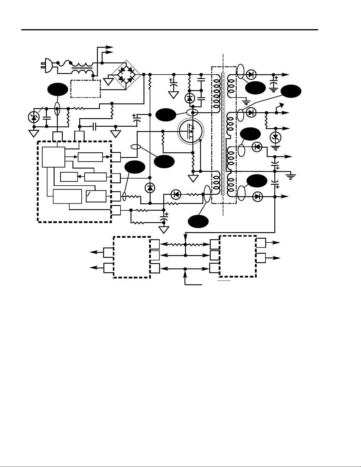
14 Main Power Supply (CTC195/197)
AC to PTV
F201
120VAC
WF51
CR108
3V
3
Control
Logic
Ref V
Ctl & Over
Load Amp
U14101
PWM Controller
L201
Degauss
Circuit
R145
R122
2
Output
C146
"V" Mon
0 Cross
Detect
Power Supply
CR210
R104
R146
C127
5
WF50
6
CR111
8
R105
1
R147
R149
C208
WF48
R111
WF49
CR102
Q101
R135
C147
R124
R148
WF52
"HOT!"
T101
Np
3
4
Nf
9
8
"HOT!"
"COLD!"
11
Ns1
13
Ns2
15
Ns3
16
12
10
Ns4
"COLD!"
WF56
WF54
CR113
WF53
CR116
CR106
CR107
+31V
(Stdby)
WF55
TP14101
+140V
(Stdby)
+33V
(Stdby)
CR133
33V
-12V
(Stdby)
+16V
(Stdby)
+5V
(Run)
+12V
(Run)
7
6
U14701
Main
Reg
Fig. 2-1 Main Power Supply
See Waveforms Page 21.
2
1
3
2
U27905
1
3
RUN/STBY
FPIP
Reg
(from Sys Ctl U13101-19)
7
6
+5V
(Run)
+12V
(Run)
Page 15

Main Power Supply (CTC195/197) 15
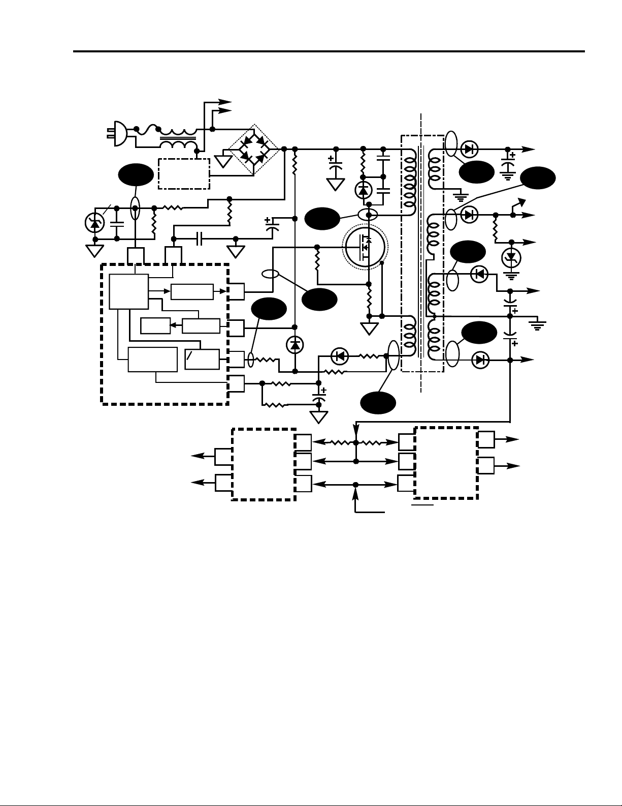
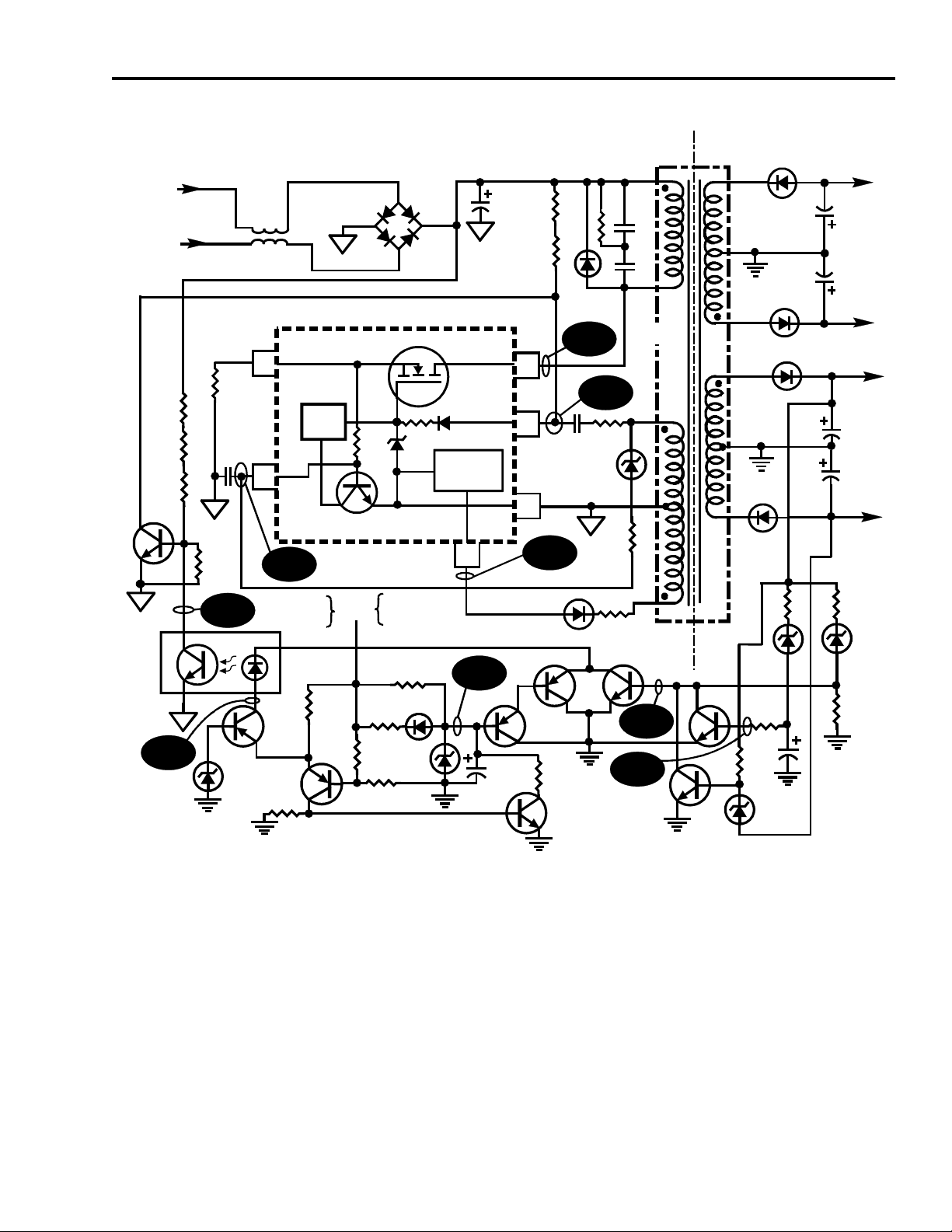
CTC195/197 “Main” Power Supply
The CTC195 and CTC197 main power supply is a variable frequency/variable
pulse width switch mode power supply (refer to Fig. 2-1). It uses a power supply
controller IC (U14101) that drives the power MOSFET, Q101. The CTC195 &
CTC197 are “cold” chassis and the electrical isolation between the power supply
and chassis is achieved using the ferrite core transformer, T101. Energy is stored
in the transformers primary winding during the power MOSFETS On time and is
transferred to the secondary windings when the MOSFET switches off (flyback
period). The transformer (T101) must expend all it’s stored energy before the
start of the next “On” period of the MOSFET. The power supply is self oscillating
and the frequency is dependent on the load and the AC line voltage. The
frequency can vary between 25kHz and 90 kHz. This supply uses “hot side”
regulation which means that there is no actual physical sampling of the secondary
voltages. The feedback winding (Nf) on the hot side of the transformer is tightly
coupled to the Reg B+ windings on the secondary. Voltage variations in Reg B+
are reflected back into the feedback winding (Nf). The regulator IC U14101 has
its own internal reference voltage. The power supply operates whenever it is
connected to the AC line and supplies current on demand up to its current output
limit. The maximum input power to the supply is 180 watts. A diagram of the
power supply is shown in Figure 2-1.
AC In and Degaussing
The AC input to the supply is passed through fuse F201 and then choke L201. It
then enters the bridge diode, CR210. C208 is the Raw B+ filter capacitor and the
unregulated voltage at this point is approximately 150VDC at 120VAC input.
The degaussing circuit is connected in the line via thermistor RT201 and degauss
relay K201. Power for the relay comes from the +12V RUN2 supply. The +12V
RUN2 supply is only present when the instrument is turned on. The relay K201 is
closed and current flows through the degauss coil and thermister RT201. This
heats the thermistor and reduces the current through the degauss coil. After
approximately 1.5 seconds the current through the thermistor falls enough that the
relay de-energizes allowing the relay to open, ending the degauss cycle.
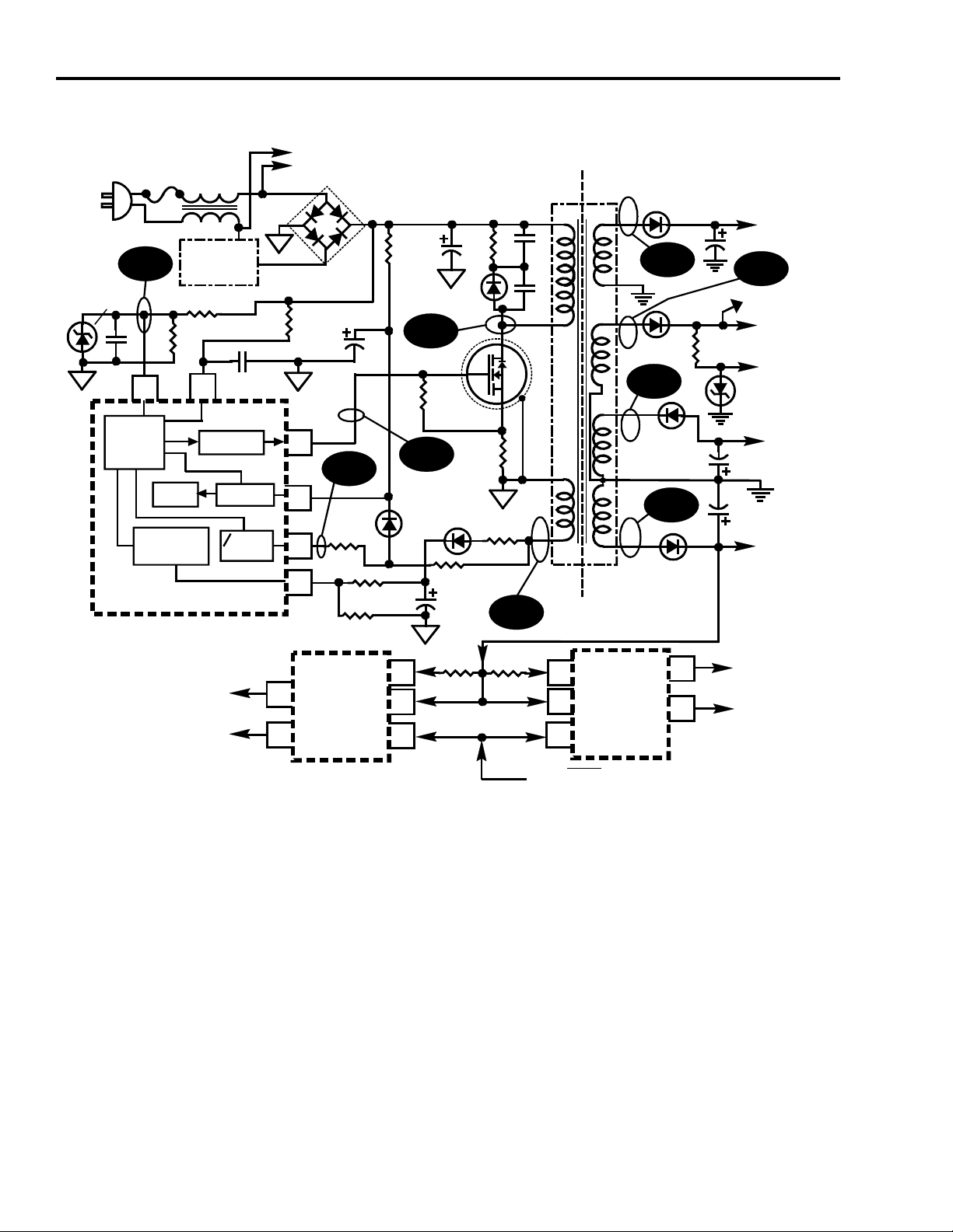
Page 16

16 Main Power Supply (CTC195/197)
Power Supply Operation
When the instrument is first plugged into an AC source, approximately 150VDC
Raw B+ is developed by the bridge rectifier diodes and the Raw B+ filter
capacitor C208. This is coupled through the primary winding (Np) of T101 (pin
3) and to the drain of the power MOSFET (Q101) via pin 4 of the transformer.
The source of the MOSFET is connected to ground through R124 (.22 ohm/2
watt). At the instant that the instrument is plugged in, the power supply is not
operating and IC U14101 needs a source of power to turn on Q101 the first time.
IC U14101 pin 6 (Vcc) receives B+ via resistor R104 which is connected to raw
B+.
With B+ applied to pin 6 of the regulator, U14101 outputs a voltage at pin 5 that
is applied to the gate of Q101. This turns the MOSFET (Q101) on for the first
time and results in a current flow through the primary (Np) of T101 and Q101.
The IC senses this current indirectly using a circuit consisting of C146 and R146.
One side of R146 is connected to Raw B+ while the other side is connected to
C146 to form a simple RC network. This network is connected to pin 2 of
U14101. This is the primary current sensing input. The capacitor is held in a
discharged state by pin 2 of IC U14101 until the gate of the MOSFET is turned on
at which time C146 is allowed to start charging. With the MOSFET turned on, the
current increases through it and the voltage on pin 2 of the IC also starts to
increase. When the voltage at pin 2 reaches approximately 3 volts, the IC shuts
off the drive to the MOSFET. At this point, the energy stored in the primary of
transformer (Np) is transferred to the secondary windings. At the same time, the
energy transfer is also coupled back into the feedback winding (Nf) between pins
8 and 9. The voltage developed at pin 8 of T101 is rectified by CR111 and filtered
by C127. This voltage is applied to pin 6 (Vcc) of U14101 and now serves as the
Run Vcc instead of the voltage across R104. The voltage across R104 is only
used during initial start-up. After all of the energy is depleted in the secondary
windings, the voltage at pin 8 of T101 starts to decay down to zero. This
decreasing voltage is applied to pin 8 of the IC through R105. This is the zero
crossing input to the IC. When this waveform goes through zero, it signals the
start of another cycle and the IC turns the power MOSFET back on. Current will
again start increasing through Q101 and the voltage on pin 2 of the IC starts
increasing again.
Once the power supply is operating, a method is needed to regulate the output
voltages. This is accomplished by the feedback input at pin 1 of IC U14101. The
winding on pins 8 and 9 of T101 serves three functions. As already explained, it
serves to power the IC and also serves as the zero crossing input to the IC. Its
third function is to provide voltage feedback information from the secondaries
back to the IC. The physical construction of the transformer is such that the
feedback winding is tightly coupled to the Reg B+ winding on the secondary. For
this reason, the voltage across the winding Nf closely follows the voltage
fluctuations on the secondary. This voltage is rectified by CR102 and filtered by
C147 where it is applied to a precision voltage divider. This divider is formed by
R147 and R149. The output of the divider is connected to pin 1 of the IC U14101.
If this voltage exceeds 400 mV, the IC terminates the drive signal to the MOSFET.
Page 17
F201
120VAC
WF51
CR108
3V
3
Control
Logic
Ref V
Ctl & Over
Load Amp
U14101
PWM Controller
L201
Degauss
Circuit
R145
R122
2
Output
C146
"V" Mon
0 Cross
Detect
AC to PTV
Power Supply
CR210
R146
C127
5
WF50
6
CR111
8
R105
1
R147
R149
R104
C208
WF48
WF49
R111
Q101
CR102
R135
C147
Main Power Supply (CTC195/197) 17
"HOT!"
T101
R124
8
R148
WF52
"COLD!"
CR116
Ns1
Ns2
Ns3
11
13
15
WF54
16
12
WF56
CR106
CR113
+31V
(Stdby)
WF55
TP14101
+140V
(Stdby)
+33V
(Stdby)
CR133
33V
-12V
(Stdby)
Np
3
4
Nf
9
WF53
Ns4
"COLD!""HOT!"
10
CR107
+16V
(Stdby)
+5V
(Run)
+12V
(Run)
2
U27905
1
3
RUN/STBY
FPIP
Reg
(from Sys Ctl U13101-19)
7
6
U14701
Main
Reg
2
1
3
Fig. 2-1 (Repeated) Main Power Supply
See Waveforms Page 21.
7
6
+5V
(Run)
+12V
(Run)
Page 18
18 Main Power Supply (CTC195/197)
AC to PTV
F201
120VAC
WF51
CR108
3V
3
Control
Logic
Ref V
Ctl & Over
Load Amp
U14101
PWM Controller
L201
Degauss
Circuit
R145
R122
2
Output
C146
"V" Mon
0 Cross
Detect
Power Supply
CR210
R104
R146
C127
5
WF50
6
CR111
8
R105
1
R147
R149
C208
WF48
R111
WF49
CR102
Q101
R124
R135
C147
R148
WF52
"HOT!"
T101
Np
3
4
Nf
9
8
"HOT!"
"COLD!"
11
Ns1
13
Ns2
15
Ns3
16
12
10
Ns4
"COLD!"
WF56
WF54
CR113
WF53
CR116
CR106
CR107
+31V
(Stdby)
WF55
TP14101
+140V
(Stdby)
+33V
(Stdby)
CR133
33V
-12V
(Stdby)
+16V
(Stdby)
+5V
(Run)
+12V
(Run)
7
6
U14701
Main
Reg
Fig. 2-1 (Repeated) Main Power Supply
See Waveforms Page 21.
2
1
3
2
U27905
1
3
RUN/STBY
FPIP
Reg
(from Sys Ctl U13101-19)
7
6
+5V
(Run)
+12V
(Run)
Page 19

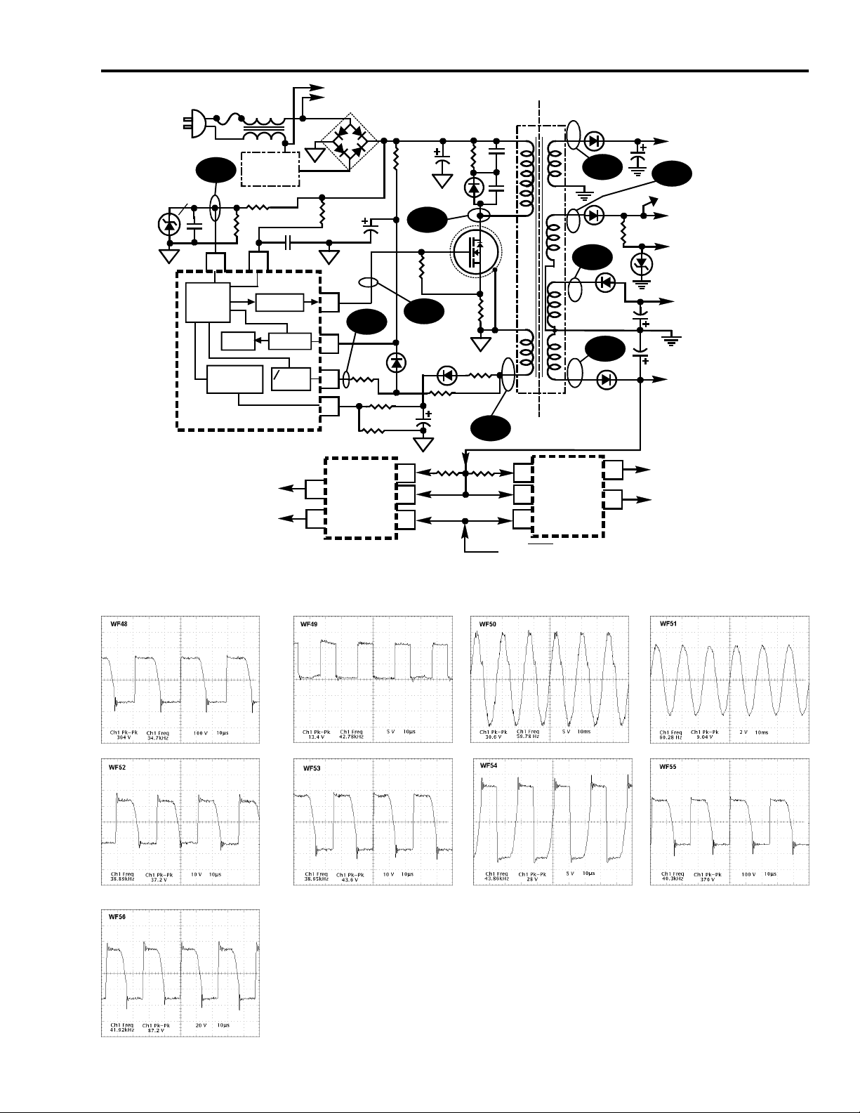
Main Power Supply (CTC195/197) 19
In this way the output drive signal from pin 5 of the IC is regulated so that 400mV
is maintained at pin 1 of the IC. The voltage divider is adjusted so that this
corresponds to the required Reg B+ (»140VDC).
There are two ways of turning off the MOSFET. First, by exceeding 400mV on
pin 1. Second, the voltage on pin 2 (primary current sense) exceeds 3 volts. Pin
1 senses the output voltage while pin 2 limits the maximum output current. If the
output load increases, then more energy must be stored in the primary of the
transformer. This requires the MOSFET be turned on longer. If it is on too long,
C146 on pin 2 charges above 3 volts and shuts off the drive to the MOSFET,
acting as overcurrent protection.
Now let’s take a look at some of the other components in the power supply. R145
and R122 form a voltage divider from raw B+. This voltage is applied to pin 3 on
the IC and forms a “Voltage In” monitor. If the voltage on pin 3 falls below
approximately 1.0 volt the supply shuts down. This is to protect against “Low
Line” voltages. The R/C/Diode network across pins 3 and 4 of T101 form a
snubber network to help dampen any ringing when Q101 turns on and off.
Secondary Supply Operation
The output voltages on the secondary side of the supply are +140, +16, -12, and
the audio supply which varies depending on which audio system in the unit. The
secondary supplies are operational as long as AC power is applied to the instrument.
Each of these voltages are provided by an individual winding on the transformer
with a single rectifier/filter combination.
A 33 volt low power supply for the tuner is derived from the +140V supply. This
supply is composed of a 33 volt zener diode and filter capacitors. A switchable
+12 and +5 volts are provided by regulator U14701. These are both derived from
the +16 volts. Pin 1 is the +16V input while pin 2 is the input for the +5V. The
+16V at pin 2 is passed through a resistor which drops the +16 down to a lower
value reducing the amount of dissipation in the IC. The outputs are filtered before
being sent to the respective circuits. A unique feature of the IC is that their
outputs are switchable (on or off) by a TTL control signal from the system control
circuit. The outputs of regulator IC can be turned off by pulling pin 3 low. IC
U27905 is the same type of regulator as U14701 but provides the supplies for the
FPIP module.
Page 20

20 Main Power Supply (CTC195/197)
Troubleshooting
Many of the malfunctions in the power supply can be quickly resolved with
simple resistance and voltage measurements. However step-by-step check lists
for some of the more common problems are provided below. One item in particular
deserves special attention. If the main supply is not running, first check for
presence of Raw B+. This can be checked at the +/- terminals of the Raw B+
capacitor C208. There should be approximately 150VDC at this point. If Raw
B+ is present, connect an oscilloscope to pin 6 of U14101. If you see a oscillating
or varying waveform of approximately 4.5 volts to 12 volts, then the IC is not
getting enough Vcc voltage to run. As C127 charges through R104, the voltage
on pin 6 of U14101 will rise, then fall when IC U14101 attempts to turn on.
At this point, it will begin to output pulses on pin 5 of the IC to turn on Q101. If
the supply does not start the voltage on pin 6 starts to decay and the IC turns off.
This process then repeats itself. The result is an oscillation on pin 6. The most
likely cause is an open CR111. If CR111 is shorted, the voltage on pin 6 would
be very low and there would be no oscillation. In any case, if the voltage is
oscillating on pin 6 then the supply is not starting or is trying to start but not
getting enough Vcc from pin 8 of the transformer to pin 6 on the IC.
Another important area that needs to be addressed is what happens to the power
supply during a heavy load or a short on one of the outputs. During heavy load the
voltage ramp on pin 2 of U14101 exceeds 3 volts and the supply shuts down in the
current limit mode. At this point the power supply then tries to restart and if the
load (or short) is still present, it shuts down again. This sequence repeats itself at
an interval of approximately 1/2 second. A large amount of current will be
flowing through the primary of the transformer as the supply tries to restart which
results in an audible “chirp”. If you hear this, suspect a short on one of the
secondaries such as a shorted horizontal output transistor, etc.
Symptom: Fuse Opens
Check for shorted Q101. If shorted, replace Q101 and check R124. If Q101 not
shorted, check CR210 (bridge rectifier) for short.
If fuse opens again, suspect U14101 and varify Q101.
Symptom: No Raw B+
Check fuse F14201. If open, replace and check Raw B+. If fuse OK, check for
output from bridge diodes (CR14210). If bridge OK, check surge resistor R14203.
Symptom: No Secondary Supplies
Check Raw B+. If Raw B+ not present, go to No Raw B+ check above.
If Raw B+ OK, use scope and check U14101-6 for oscillation. If oscillation
present check for open CR111 or R135. If oscillation not present go to step 3.
Is power supply “Chirping”? If yes, check for shorts on the secondary side of
supply. If no, check for shorted CR111 or shorted R135.
Page 21
F201
120VAC
WF51
CR108
3V
3
Control
Logic
Ref V
Ctl & Over
Load Amp
U14101
PWM Controller
L201
Degauss
Circuit
R145
R122
2
Output
C146
"V" Mon
0 Cross
Detect
AC to PTV
Power Supply
CR210
R146
C127
5
WF50
6
CR111
8
R105
1
R147
R149
R104
C208
WF48
WF49
R111
Q101
CR102
R135
C147
Main Power Supply (CTC195/197) 21
"HOT!"
"COLD!"
R124
R148
WF52
T101
Np
3
4
Nf
9
8
Ns1
Ns2
Ns3
Ns4
"COLD!""HOT!"
11
13
15
16
12
10
WF56
WF54
CR113
WF53
CR116
CR106
CR107
+31V
(Stdby)
WF55
TP14101
+140V
(Stdby)
+33V
(Stdby)
CR133
33V
-12V
(Stdby)
+16V
(Stdby)
2
1
3
RUN/STBY
U27905
FPIP
Reg
(from Sys Ctl U13101-19)
+5V
(Run)
+12V
(Run)
7
6
U14701
Main
Reg
2
1
3
Fig. 2-1 (Repeated) Main Power Supply
+5V
7
6
(Run)
+12V
(Run)
Main Power Supply Waveforms
Page 22

22 Main Power Supply (CTC195/197)
Auxiliary Power Supply Operation
The auxiliary power supplies on the Main CBA consist of three (3) regulator IC’s
U14104 (+7.5VDC), U18101 (3.3VDC) and U14601 (+5VDC). Series pass
transistor regulator Q11600 provides the +9.5VDC supply. U14104, U18101 and
Q11600 obtain their input voltages (+12V & +5V) from Main Regulator U14701.
These power supplies are only On when U14701 is power up, which occurs only
when the instrument is turned on. Regulator IC U14601 uses the +16VDC supply
from the Main Power supply and outputs the StandBy +5V for the microcomputer
and EEPROM. This power supply is always present whenever the instrument is
plugged into AC power.
Page 23

Main Power Supply (CTC195/197) 23
TP14103
+12V
6
U14701
Main
Reg
(Main Pwr Supply)
7
+5V
+16VDC Stdby
DeCoder PCB
(+12V)
(+16V)
TP14601
3
+10V Reg
+9.5V
Reg
C14715
C14714
U23902
Q11600
CR11600
CR14604
2
1
10V
3
1
Main PCB
U14104
+7.5 Reg
1
U18101
+3.3 Reg
U14601
+5 Reg
2
1
3
2
DeCoder PCB
3
2
+9.5VDC
(Run)
+7.5VDC
+3.3VDC
(Run)
+5VDC
C13163
+5VDC
+12VDC
+10VDC
(Run)
(Stdby)
(Stdby)
(Run)
(Stdby)
Fig. 2-2 Auxiliary Power Supply
Page 24
24 PTV Power Supply (CTC195)
120VAC
(From Main
Pwr Supply)
R0
R1
R2
Q700
4
3
WF62
R14
2W
.39
C05
WF61
U701
CR11
8.2V
Ω
T700
8
7
WF60
1
Q1
R26
U700
Amp
On/Off
Signal
2
Q2
CR717 thru
CR720
R3
+23V
R4
1.2K
R5
10K
R24
1K
R6
ZD1
TR3
From Digital
Convergence
PCB, CR200
R20
CR13
CR14
10V
10K
240K
TR1
D1
Error Det
(-40.5V Ref)
1
WF63
Q5
Q8
R22
C702
R3
11
4
3
WF59
Q3
C14
CR3
WF57
WF58
C700
CR5 R18
R25
R10
CR01
10V
R11
"HOT"
7
T701
1
"HOT"
Q4
WF64
WF65
5
2
3
Q7
Np
Nd1
Nd2
"COLD"
14
Ns1
12
9
Ns2
10
Ns3
11
13
Ns4
"COLD"
Q6
CR9
CR10
CR15
20V
R21
CR16
13V
CR7
CR8
-45VDC
+45VDC
+15VDC
-15VDC
CR12
13V
Figure 3-1 Digital Convergence Power Supply
See Waveforms Page 29.
Page 25

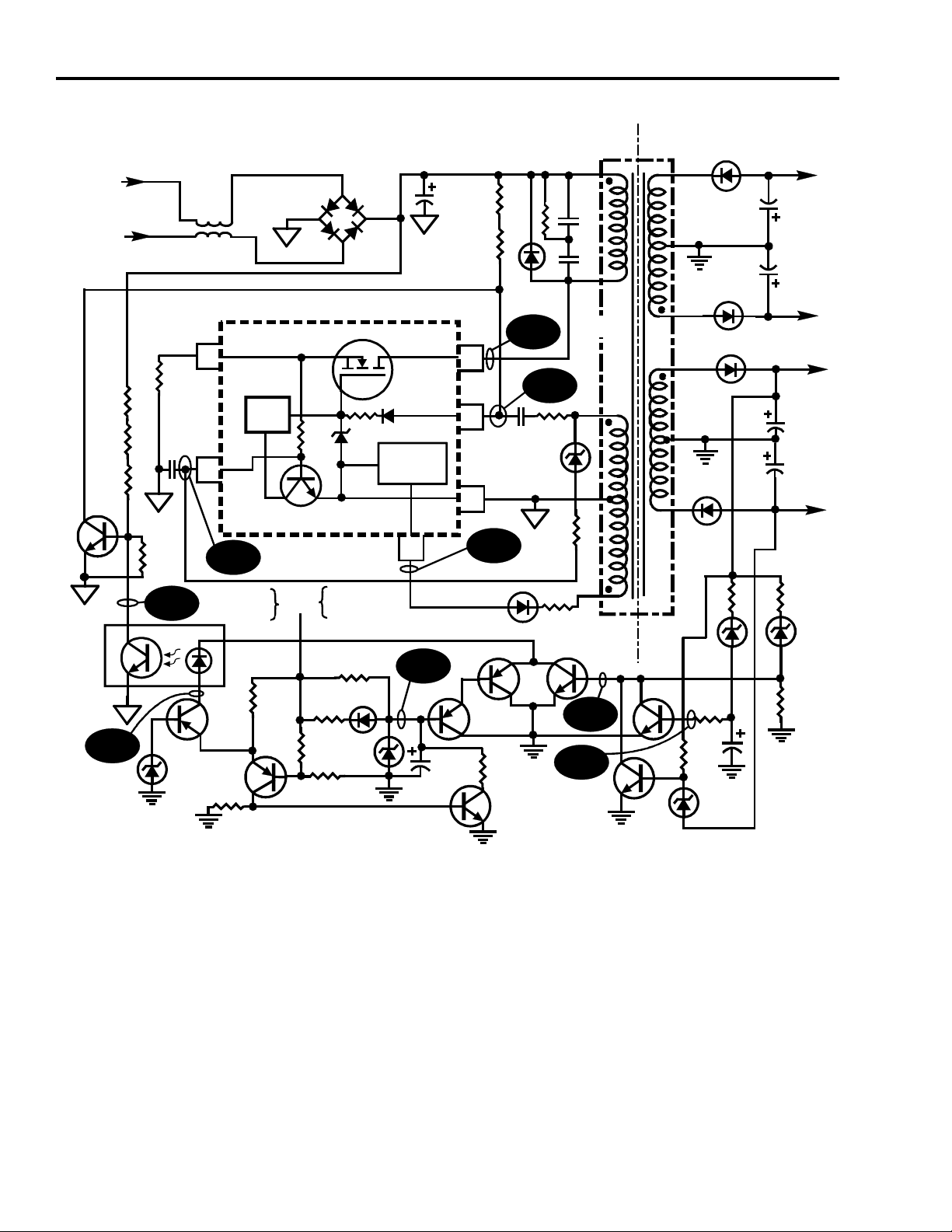
PTV Power Supply (CTC195) 25
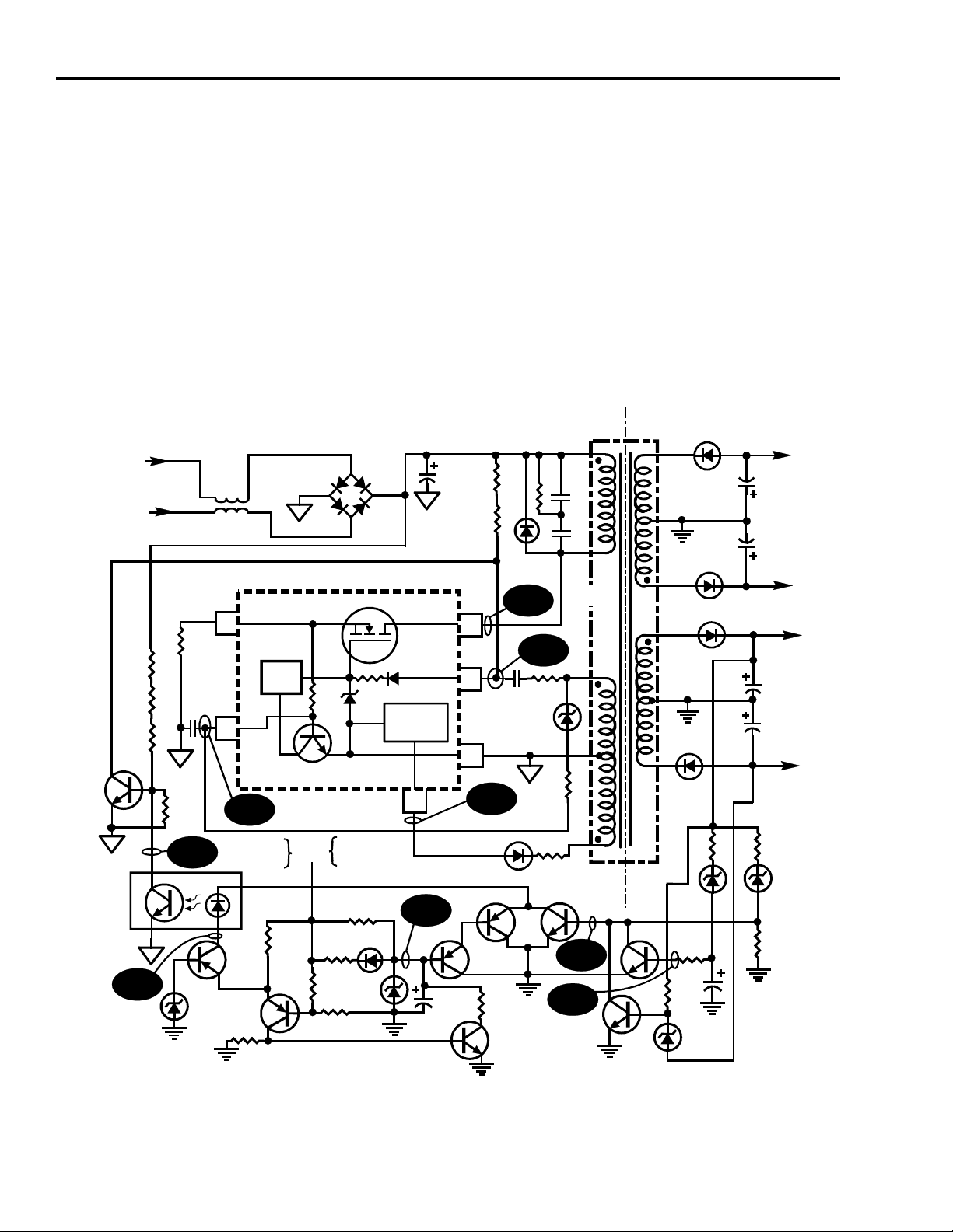
CTC195 Convergence Power Supply Overview
The convergence auxiliary power supply is a variable frequency-variable pulse
width switch mode power supply. AC power is supplied to the rectifier from the
main chassis. The Raw B+ for the PTV power supply is generated by a bridge
rectifier (CR717 thru CR720) and filtered by C702. With Raw B+ applied, the gate
of TR1 begins to charge up through R03 and R22. When the turn-on voltage of the
FET inside U700 (TR1) is reached, the FET begins conducting. With TR1
conducting, current flows through the primary (Np) of the transformer (T701), FET
(U700), and through the current sense resistor R14 (U700-8). The current flowing
through the primary winding causes a electromagnetic field to develop around the
winding of Np (pins 7 and 5). As the field around Np rises a voltage is induced into
winding Nd1 (pins 2 & 3). The voltage developed at pin 2 of T701 is coupled by
R10 and C700 to the gate of TR1 (U700-4). The polarity of this winding is such that
it generates a positive voltage which keeps TR1 conducting. When the current
through TR1 reaches the current limit threshold set by R14 and C05, TR1 is turned
off. When the FET (TR1) turns off, the magnetic field around the winding Np
collapses and the energy stored in the primary of the transformer is transferred to
the secondaries. As the field around Np collapse, a positive pulse is generated at
pin 2 of Nd1 that is applied to the gate of TR1 turning it on again. This will continue
for several cycles until stable oscillation is achieved.
The voltage developed across Nd2 rectified by CR5 and compared to an internal
reference of -40.5V (+/- .5V) at pin 1 of U700. Once operation begins, this
feedback winding controls the duty cycle of TR1. The Nd2 winding is responsible
for regulating the output voltages. The duty cycle of the power supply is altered so
that the voltage across Nd2 is maintained at -40.5V. The secondary supply voltage
windings (Ns1 through Ns4) are wound so they reflect any load changes on the
secondary back to winding Nd2.
During normal operation as the load on the power supply increases, the On time of
the FET increases. This increased On time causes higher currents to flow through
the FET and the primary winding of T701 (Np). When the voltage across R14
reaches approximately +.6V, TR3 (inside U700) turns on. This turns off the FET
and causes the output voltage to decrease. Zener diode CR01 and resistor R11 are
used to compensate for any fluctuations in line voltage that result in changes in the
Raw B+.
Page 26

26 PTV Power Supply (CTC195)
Power Supply Operation
As mentioned earlier, the power supply starts when the gate voltage of the FET (pin
4 of U700) is allowed to charge up thus turning on TR1. However, the power supply
only needs to run when the instrument is turned on. Transistor Q700 is responsible
for hold the gate of the FET low (OFF) until an On/Off signal is received from the
Digital Convergence CBA. When raw B+ is present, transistor Q700 is biased On
via R700, R701 and R702. With Q700 on, the gate of the FET is pulled low thus
preventing the power supply from starting. The On/Off signal is obtained from the
digital convergence board by rectifying the filament pulse and is approximately
+23V when the instrument is running. This On/Off signal voltage supplies the B+
to the emitter of Q1 via R4. This allows Q1 to turn on providing a current path
through the photo-diode. When the ON/OFF signal reaches approximately 16V,
Q1 allows current to flow through the photo-diode. Initially the current flowing
through the photo-diode of the opto-coupler is supplied by Q3 on the ground end
of the circuit. The components (Q5, C14 and R20) on the base of Q3 form a delay
circuit that that turns off Q3 after a short delay to allow the supply to start and
stabilize. When the +23V is present, capacitor C14 begins to charge up through
R20. As the base voltage of Q5 rises, Q5 turns off, thus turning off Q3 removing
the current path for the photo-diode. By this time the supply is up and running and
the current path for the photo-diode (ground end) is provided via Q4. This allows
the photo-transistor to remain on, keeping the base of Q700 grounded thus keeping
it turned Off. This allows the gate voltage of TR1 to rise and the power supply to
operate normally.
As mentioned earlier, the current path for the opto-coupler during normal operation
is provided by Q1 and Q4. Q4 is turned on only when the +15V and -15V supplies
are within a specific operating range. When an excessive load is put on the supply,
the supply goes into current limiting. In order not to damage the convergence
amplifiers, we need to turn off the supply whenever a major overload or overvoltage occurs. When the +15 of the -15 volt supply drops to approximately 13V
the transistor Q1 is turned off. Since Q3 is already off (after the initial startup delay)
the current path for the opto-coupler is removed. This causes the supply to
immediately turn off until the instrument is turned off and back on again. Monitoring
the +/- 45V is not required since a failure in the convergence amplifier causes a
large enough load on the supply that the current limiting circuit within U700 will
shut down the power supply. Q4 is biased on by the output of the secondary voltage
supplies. In this way the secondary output is monitored for overload on the supplies
or in the event that a supply is lost. Q4 monitors the +15V supplies for “Under 13V”
(CR12) and Q6 monitors for “Over 20V” via CR15. If the +15V secondary output
supply falls below 13V, Q4 turns off. If the +15V rises over 20V, Q6 turns on and
grounds the base of Q4, turning it off causing the power supply to shut down
because Q700 will turn back on. Q7 monitors the -15V supply via CR16. If the
-15V supply rises to -13V (supply falls) Q7 turns on grounding the base of Q4.
Whenever Q4 is turned off, this removes the current path for the photo-diode in
U700. This causes the photo-transistor in U700 to turn off allowing Q700 to turn
back on grounding the gate of the FET (TR1) thus shutting down the power supply.
Page 27
PTV Power Supply (CTC195) 27
120VAC
(From Main
Pwr Supply)
R0
R1
R2
Q700
4
3
WF62
R14
2W
.39
C05
WF61
U701
CR11
8.2V
T700
Ω
8
7
WF60
1
Q1
Q2
R26
CR717 thru
CR720
U700
Amp
On/Off
Signal
2
R4
1.2K
+23V
R5
10K
R3
TR3
From Digital
Convergence
PCB, CR200
R20
R24
1K
CR14
R6
10K
ZD1
240K
CR13
10V
TR1
D1
Error Det
(-40.5V Ref)
1
WF63
Q5
Q8
C702
Q3
C14
R22
R3
11
4
3
WF59
CR5
C700
R25
CR3
WF57
WF58
CR01
10V
R10
R11
R18
"HOT"
7
T701
Q4
WF64
WF65
5
2
3
1
Q7
Np
Nd1
Nd2
"COLD"
14
Ns1
12
9
Ns2
10
Ns3
11
13
Ns4
"COLD""HOT"
Q6
CR9
CR10
CR15
20V
R21
CR16
13V
CR7
CR8
-45VDC
+45VDC
+15VDC
-15VDC
CR12
13V
Figure 3-1 (Repeated) Digital Convergence Power Supply
See Waveforms Page 29.
Page 28
28 PTV Power Supply (CTC195)
The differential pair consiting of Q1 and Q2 alos control the turn off of the power
supply. When the On/Off voltage starts to fall, the comparator switches the current
to Q2 when the voltage falls below 16VDC. This allows current to flow into the
base of Q8, turning it on. This discharges the voltage on C14 readying it for the next
ON cycle. Since Q1 is off, current flow to the opto-coupler is stopped. With the
opto-coupler turned off, Q700 turns back on and shuts down the power supply.
Transistor Q2 is responsible for monitoring the +23 volts from the convergence
CBA. If the +23 volts starts to fall, Q2 turns on when the emitter falls below the
level that the base is biased at via R6 and R5. When Q2 turns on the emitter of Q1
is grounded, removing its B+ supply and turning it off. This instantly turns off the
opto-coupler U700. With the opto-coupler off, Q700 turns back on and shuts down
the power supply.
120VAC
(From Main
Pwr Supply)
R0
R1
R2
Q700
4
3
WF62
R14
2W
.39
C05
WF61
U701
CR11
8.2V
Ω
T700
8
7
WF60
1
Q1
R26
CR717 thru
CR720
U700
Amp
On/Off
Signal
2
Q2
R4
1.2K
10K
+23V
R5
R3
TR3
From Di gita l
Convergence
PCB, CR200
R20
R24
1K
CR14
R6
10K
ZD1
240K
CR13
10V
TR1
D1
Error Det
(-40.5V Ref)
1
WF63
Q5
Q8
C702
Q3
C14
R22
R3
11
4
3
WF59
CR5
C700
R25
CR3
WF57
WF58
CR01
10V
R10
R11
R18
"HOT"
7
T701
2
3
1
"HOT"
Q4
WF64
WF65
5
Q7
Np
Nd1
Nd2
"COLD"
14
Ns1
12
9
Ns2
10
Ns3
11
13
Ns4
"COLD"
Q6
CR9
CR10
CR15
20V
R21
CR16
13V
CR7
CR8
-45VDC
+45VDC
+15VDC
-15VDC
CR12
13V
Figure 3-1 (Repeated) Digital Convergence Power Supply
Page 29
PTV Power Supply (CTC195) 29
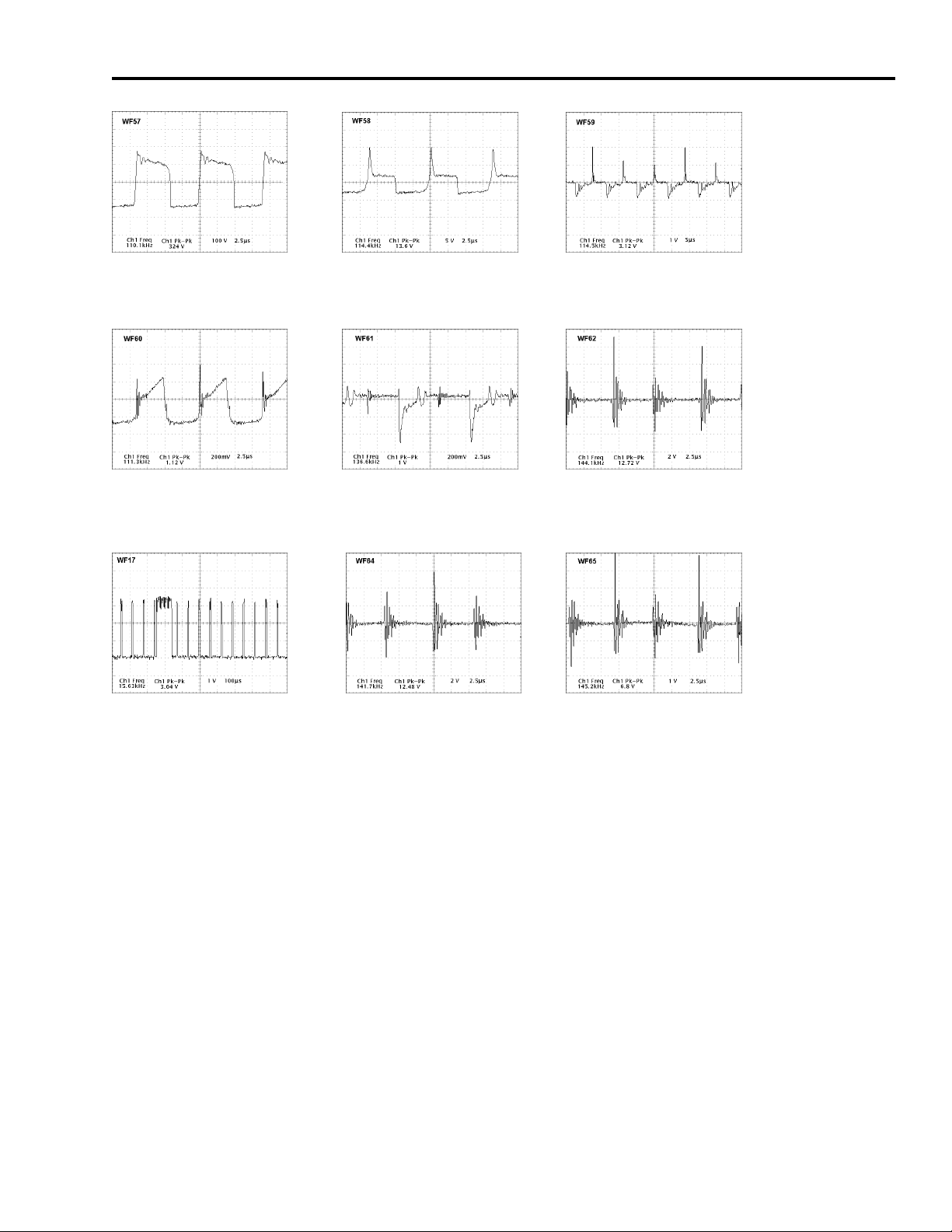
Convergence Power Supply Waveforms
Page 30

30 Horizontal Deflection
Horizontal Deflection Overview
The horizontal deflection system has two main functions in the CTC195/197 chassis.
First, it supplies the current for the horizontal yoke coils providing the energy necessary
to move the electron beam horizontally across the face of the picture tube. Second, it
provides a number of power supplies needed for operation of the chassis and picture
tube.
The horizontal yoke current is provided by a circuit consisting of a switch (HOT), the
primary inductance of the IHVT, a retrace capacitor, the trace capacitor (S-Shaping
capacitor), and the horizontal yoke coils.
The voltage supplies provided by the horizontal deflection system are derived from
secondary and tertiary windings on the IHVT. From the previous discussions of the
power supplies, they are used by the video amplifier, the tuner, the CRT, and the
vertical amplifier.
The low level signal processing circuits for the horizontal deflection system are contained
in the T4 Chip. These include the horizontal sync separator and a two-loop horizontal
AFPC system. The T4 allows bus control of several parameters associated with the
horizontal deflection system including horizontal drive pulse width, AFC Gain, Sync
Kill, and ON/OFF.
The XRP circuit in the CTC195/197 is similar to that of CTC179 and CTC185. A
peak detector sets a latch in the T4 Chip. The latch can then be reset only by I2C
communication.
The T4 Chip also generates the ramp waveform used to drive the vertical amplifier.
Bus-controlled vertical parameters include DC bias, amplitude, linearity, and
S-Correction. The same ramp that is used to generate the vertical driving waveform is
also used to create the parabola used for East-West pin correction. Bus controllable
parameters in East-West pin correction include bias (width), amplitude (pin), tilt, and
top and bottom corner. These same parameters are adjustable in both the CTC195
and CTC197. The CTC195 uses a slightly different method to achieve proper
adjustment due to the Digital Convergence system. Discussion on that is provided in
the Digital Convergence section of this manual.
East-West pincushion correction and horizontal width adjustment are provided by a
diode modulator for the direct view CRT assemblies that do not include yoke pin
correction. The modulator is driven by a linear pincushion driver. The parabola used to
develop the correction waveform is generated in the T4 Chip. The T4 provides bus
control of the horizontal width and pin amplitude as well as horizontal trap and corner
correction. In addition, a voltage developed across the high voltage return resistor is
summed at the pin driver to compensate for the decrease in width that occurs as the
high voltage increases with decreased beam current.
A new feature in the CTC197 chassis is the bus controlled Z-Axis correction. This will
allow Z-Axis correction via the remote control, making it much easier for the user than
prior back panel switches. This circuit is used in 32" and larger direct view instruments.
Page 31

Luma
In
Horizontal Deflection 31
Divide
by 16
On/Off
FlyBack
Pulse
38
23
Sync
Sep
H-Lock
Det
Phase
Det
Ramp
Gen
IC16201 T4-Chip
Loop
Filter
Phase
Det
32XH
VCO
Duty Cycle Ctl
Horz
Drive
Phase Ctl
Horz Drive Output
Figure 4-1 T4 Chip Low Level Horizontal Processing
The T4 Chip employs a two loop horizontal AFC system. The first loop is used to lock
an internal 1H (standard horizontal rate) clock to the incoming horizontal sync signal.
The second loop is used to lock the 1H clock to a feedback pulse derived from a
secondary winding on the IHVT. As with the other T-Chip versions, a horizontal-tovideo phase control is available via the I2C bus. The phase control can be used as a
horizontal centering control during instrument alignment.
XRP
Divide
by 2
POR
Horz
Out
22
The first loop employs a 32H (32 times the Horizontal Frequency) VCO referenced to
a 503 kHz ceramic resonator. To offset sync confusion caused by various copy
protection schemes, the T4 Chip provides a ±4 µsec window to capture sync and
ignore other pulses.
U16201 (T4-Chip) performs the low level horizontal processing. The functions
performed in U16201 are very similar to previous chassis. The horizontal processing
circuits contained in U16201 are:
• Horizontal Automatic Frequency Control (AFC)
• Horizontal Automatic Phase Control (APC)
• Horizontal Drive
• East West (EW) Pincushion Correction
• X-ray Protection
• Horizontal Vcc Standby Regulator
Page 32
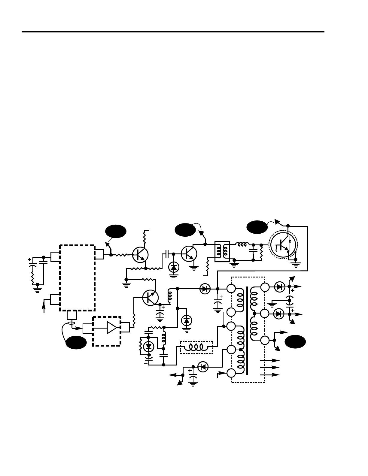
32 Horizontal Deflection
Horizontal Circuits
AFC and APC
The purpose of the AFC (Automatic Frequency Control) and APC (Automatic Phase
Control) is to maintain proper synchronization between the beginning of horizontal scan
and the incoming sync signal. The T4 Chip employs a “two-loop” approach to
accomplish this task. The first loop is the AFC and second loop is the APC. The AFC
phase locks the horizontal oscillator to the incoming sync signal frequency. The APC
locks the phase of the horizontal output to the phase of the horizontal oscillator. This
system is superior to previous designs because it is continuously adjustable for excellent
noise immunity in the presence of marginal input signals and can track rapid phase
changes in signals from VCR’s or similar devices. The external circuit at pin 21 of
U16201 is the loop filter for the phase lock loop (PLL) and is used to optimize the
frequency response of the AFC loop.
The APC loop is used to track out the phase errors due to variable delays in the
horizontal driver and output circuit. The APC has a two bit register (APC Gain) that
controls the gain of the APC loop. APC Gain, like AFC Gain, is preset at the factory
and cannot be adjusted by the service technician. The reference signal for this loop is a
flyback pulse applied to an RC network and input to U16201 pin 23.
Flyack
Pulse
21
23
AFC
TP14302
H-Out
T-Chip
Y/C
Deflection
U16201
E/W
Pin
17
WF38
3
WF36
22
U14801
Q14302
H-Amp
Q14802
C14805
7
CRT Driver Volt
+16V
H-Driver
TP14703
WF37
Q14301
CR14402
+150V
C14715
CR14800
H-Yoke
CR14702
TP14301
T14301
3
1
Reg B+
6
5
T14401
2
14
1
6
3
WF35
IHVT
Q14401
Horz Out
CR14701
10
9
CR14703
8
TP14402
TP14704
+26V
+13V
TP14706
Fil Pulse
WF33
TP14303
Focus
Anode HV
Screen
Figure 4-2, Horizontal Circuitry Block Diagram
Page 33

Horizontal Deflection 33
Horizontal Driver
The horizontal driver circuit serves as an interface between the low level horizontal
output of the T4 Chip and the high power horizontal output circuit. The driver operates
in a typical flyback configuration. Energy is stored in the driver transformer, T14301,
during the conduction cycle of Q14301. When Q14301 turns off, the stored energy is
dumped into the base of Q14401, the horizontal output transistor (HOT). A buffer
stage, Q14302, has been added between the horizontal driver, Q14301, and the
T4 Chip to reduce the amount of current that must be handled by the T4 Chip output
stage.
Horizontal Output
The horizontal output circuit generates the high current ramp waveform used to drive
the horizontal yoke. It also drives the flyback transformer, which in turn produces the
hi-voltage supplies necessary for picture tube operation. The supplies include hivoltage, focus supply, screen supply, cathode B+, and the heater voltage. Additional
secondary supplies are provided for use by the vertical amplifier.
Horizontal Waveforms
Page 34

34 Horizontal Deflection
Luma In
38 16
2H
Sync
Sep
X
X
E/W
Corner
Vert
Count
Down
Tilt
Σ
E/W
ALC In
Vert Blanking
Ramp
Gen
E/W
Ampli-
tude
"V" to "I"
Transform
"V" to "I"
Transform
E/W DC
E/W Pin
Correction
Linearity
S-
Correct
E/W Pin
Output
Vertical Output
Figure 4-3, T4 EW Pin Correction Processing
17
Vert Kill
Σ
Vert
DC
Vert
Size
Vert
Output
15
Horz from
T14301-6
Q14401
Horz Out
E/W Pin
Drive from
U14801-7 &
T-4 Chip
E/W Pin
Buffer
Q14802
C14405
CR14401
C14404
L14801
C14805
R14403
R14401
CR14402
L14402
C14403
C14715
CR14800
TP14402
T14401
2
14
H-Yoke
Figure 4-4, E/W Pin Correction Modulator and Components
(CTC197 Only)
Page 35

Horizontal Deflection 35
E/W Pin Correction & S-Correction (CTC197)
The horizontal processing circuits of the T4 contain provisions for geometry correction
including vertical linearity correction, vertical S-correction, and EW pin correction.
Horizontal linearity correction is provided by the linearity coil, L14402. The parallel
damping network consisting of C14405 are included to reduce ringing in the linearity
coil at the beginning of scan. S-correction is achieved inside the T4 Chip and further by
the S-capacitor, C14404. Another parallel network is added to the S-capacitor to
reduce further raster deformations. This network consists of C14401, R14401, and
C14403. EW pin correction is done by a diode modulator circuit. Figure 4-4 is a
simplified schematic which illustrates the principle of the diode modulator.
Note: EW pin correction is not needed in 25" and 27" IR sets. These sets use pin
corrected horizontal yokes.
Figure 4-4 shows the circuit arrangement of the diode modulator. The pin correction
circuit controls the voltage at the junction of L14801 and C14805. Since the amount of
horizontal scan is proportional to the voltage across the S-capacitor, C14404, the pin
circuit can control the amount of horizontal scan by controlling the voltage at the bottom
of C14404. The voltage at the top of C14404 is essentially held at reg B+. To achieve
pin correction, a vertical rate parabolic waveform is produced by the pin circuit and
applied to the S-capacitor, C14404. This, in turn, produces the desired modulation of
the horizontal scan. Another feature of the diode modulator is that it allows width
adjustment. This is achieved by varying the dc voltage at the bottom of the S-capacitor.
E/W Pin Correction & S-Correction (CTC195)
E/W Pin Correction and S-Correction are accomplished differently in the projection
chassis version CTC195 chassis. See the chapter on Digital Convergence for an
explanation of this circuit.
Page 36

36 Horizontal Deflection
T-Chip
Y/C-Deflection
Horz
Output
U16201
WF33
Filament
From IHVT
T14401-8
TP14303
22
To H-Amp
Q14302
WF36
24
XRP SW
Q14901
R14904
R14905
R14908
R14909
R14907
R14910
10V
CR14902
!
BC14901
CR14901
WF34
TP14901
Fig 4-5, XRP Block Diagram
X-Ray Protection Circuit
The X-Ray Protection (XRP) circuit used in the CTC197 is contained in the T4 Chip.
The input for XRP is pin 24 and is used to turn the Horizontal Drive Output on and off.
A reference voltage of 3 Volts ±12 mV (4%) is generated inside the T4 chip. The
reference voltage is produced by a bandgap reference, which is very stable even under
temperature differences. If the voltage at pin 24 exceeds the 3 volt reference, a latch is
set inside the T4 which inhibits, or turns off, the horizontal output circuit. This action
defeats the ability of the chassis to produce high voltage, thus eliminating an X-ray
threat.
The XRP detector voltage is produced by a secondary winding, pin 8, on the IHVT.
This output is designed to closely track high voltage. The pin 8 voltage is peak detected
by CR14901, thus producing a dc voltage proportional to the high voltage. This
voltage is applied to the precision resistor divider consisting of R14907 and R14908.
The values of the divider are carefully chosen to produce the correct XRP trip threshold
for each picture tube. If the voltage across R14907 becomes large enough, Q14901
turns on, allowing current to flow through R14905. When the current becomes large
enough, the voltage at R14905 exceeds the 3 volt level of the XRP comparator in the
T4 Chip and the XRP latch is set.
The only way to reset the XRP latch is by a transition of the T4 on/off register. To
restart the horizontal output after an XRP trip, it is necessary for the micro to send the
T4 an “off” command, then an “on” command. For a typical XRP trip, the micro will try
to restart the horizontal output after a short time delay of around 1.5 seconds without
user intervention. However, if the micro counts three of these attempted restarts within
a minute, the system shuts down and an error, 8 (XRP) will be logged. At this point it
is necessary for the customer to turn the set back on via the front panel or the remote.
Page 37

Horizontal Deflection 37
Z-Axis Correction
The Z-Axis correction circuit is used to counteract raster rotation when the picture tube
is oriented in a north or south direction. This is accomplished by adding a DC magnetic
field to counteract the Earth’s magnetic field.
On 32" screen sizes and larger, the CTC197 will use a microprocessor controlled
approach to Z-Axis correction. The microprocessor controlled approach is superior to
the back cover switch approach in several ways. First, it frees valuable space in the
back of the instrument since no manual adjustment is required. It also allows adjustment
to be performed from the front of the receiver making control much easier for the
service person or the customer. Also, since the control circuit utilizes an eight-bit D to
A, much finer resolution is possible. Linearity of the output and sensitivity to component
variations was improved by using the approach shown in the figure below.
Vert
1/2Sup
Tilt D/A
+26V
Run
7
3
U14275
Q14276
6
2
4
Q14275
Figure 4-6, Z-Axis Correction Circuit
J14275
1
2
Vert
1/2Sup
Page 38

38 Horizontal Deflection
Troubleshooting
Dead Set
A failure in the horizontal circuitry will most likely cause a dead set symptom.
1. Check the collector of Q14401 for +140 volts. If missing, check for a shorted
Q14401 and troubleshoot the power supply. If present, go to the next step.
2. Check for 7.6 volts on pin 20 of U16201. If it is not there, check the 12 volt
standby supply. If it is there go to the next step.
3. Check pin 22 of U16201 for horizontal drive pulses when the power button is
pressed. If no pulses are seen, see dead set troubleshooting in the “System
Control" section of this publication. If they are present, go to the next step.
4. Check for horizontal drive pulses on the emitter of Q14302 and the collector of
Q14301. If they are missing, check the corresponding stages. If they are present,
go to the next step.
5. Check the drive to signal to the base of the horizontal output transistor, Q14401. If
it is present, suspect a defective Q14401. If it is not, suspect a defective T14301
No Horizontal Sync
1. Make sure the problem is a horizontal sync problem by comparing the horizontal
drive signal to incoming video sync (one complete horizontal drive cycle begins and
ends with the horizontal sync in the video).
2. Check for the AFC feedback signal to pin 23 of U16201. If missing, trace it back
to T14401, the IHVT. If the signal is present, go to the next step.
4. Check the AFC filter voltage on pin 21 of U16201 with service data. If it is
incorrect, suspect the components off pin 21.
Page 39

Flyack
Pulse
21
23
AFC
TP14302
H-Out
T-Chip
Y/C
Deflection
U16201
E/W
Pin
17
WF38
3
WF36
22
U14801
Q14302
H-Amp
Q14802
C14805
7
CRT Driver Volt
+16V
H-Driver
TP14703
WF37
Q14301
CR14402
+150V
C14715
CR14800
H-Yoke
CR14702
TP14301
T14301
3
1
Reg B+
Horizontal Deflection 39
TP14402
WF35
6
5
Q14401
Horz Out
T14401
2
14
1
6
3
CR14701
10
9
CR14703
8
IHVT
TP14704
+26V
+13V
TP14706
Fil Pulse
WF33
TP14303
Focus
Anode HV
Screen
Figure 4-2 (Repeated), Horizontal Circuitry Block Diagram
Horizontal Waveforms
Page 40

40 Vertical
See Waveforms Page 44
V-Sync to
SysCtl
WF26
WFXX
Vert
Out
T-Chip
Y/C
Deflection
U16201
Vert
VCC
U13101-34
TP14502
15
R14508
+7.5
26
R14509
WF27
2
1
7
8
WF25
3
RN4501
TP14504
+13V
Q14501
V-Sync
6
4
5
C14502
3
1
7
R14519
R14517
R14518
6
U14501
Vert Out
WF24
1/2 Supply
R14515
2
4
5
TP14501
+13V
+26V
1.5
R14507
Figure 5-1, Vertical Deflection Circuit
Vert
Yoke
Vertical Circuits
The vertical circuit in the CTC195/197 is very similar to the CTC179/189 and
the earlier CTC177 vertical circuits. Like the earlier chassis, the output amplifier is DC coupled instead of capacitively AC coupled. The DC coupled circuit
has the advantages of fewer parts, lower cost and linearity becomes less dependent on electrolytic capacitor tolerance and aging. “S” correction, the tendency
of the horizontal lines to be spaced closer at different points in the screen, is
accomplished inside the T4-chip.
Because of DC coupling, the DC level of the vertical reference ramp from
U16201 pin 15 affects vertical centering. This allows vertical DC (vertical
centering) to be included in the digital alignments. By moving the vertical ramp
higher or lower around a DC voltage, vertical centering can be accomplished.
This also compensates for tolerances in the reference ramp DC voltage.
The vertical circuit acts as a voltage to current converter. It changes the vertical
rate DC ramp signal out of the T-Chip to a current ramp through the yoke to
deflect the electron beam from top to bottom on the CRT. Figure 5-4 shows a
typical output waveform from the T-Chip and other waveforms associated with
the vertical circuitry. The vertical output IC, U14501, is an inverting amplifier
that sinks current at pin 5 when pin 1 is high and sources current from pin 5 when
pin 1 is low. U14501 is supplied by the 26 volt run source from the main power
supply.
Page 41

Half-Supply
An important aspect of the vertical circuitry is the "half supply". It is connected
to the low side of the yoke and remains at approximately half of the 26 volt
supply. The supply is developed from a secondary winding of the IHVT and
CR14703. The 26 volt supply is taken from a portion of the same winding which
means the 26 volt and the 13 volt supply track each other. The purpose of the
half supply is to provide a reference voltage to the vertical circuitry, around
which yoke current is generated. The current through the yoke must travel in two
directions. First, during the active portion of scan, current flows in such a
direction to cause the beam to travel down the face of the CRT. During retrace,
the yoke must stop the downward travel of the beam and return it to the top of the
screen by reversing the yoke current. The beam travels down the screen in 1/60th
of second, but has to return to the top in much less time. The vertical circuitry
uses some tricks to accomplish the task.
Vertical 41
R14508 and R14509 limit the current in the yoke to keep the beam from
deflecting off the screen in the event U14501 might short to ground or to the 26
volt source. C14502 acts as a filter and with R14518 helps reduce the vertical
rate ripple current on the “half supply.” R14519, whose value is less than one
ohm, and R14502, (which is in parallel to provide finer adjustment), form a
current sense resistor that develops a voltage drop directly proportional to yoke
current. The half supply is input to pin 5 of RN4501 and through R14519 to pin
4 of RN4501. The bias voltage at RN4501 pin 5 goes out pin 6 to the vertical IC
noninverted input at U14501 pin 7. The bias voltage at RN4501 pin 4 goes out
pin 3 to the inverted input of the vertical IC, U14501 pin 1. The helps to cancel
any modulation of the half supply resulting from vertical rate current on
C14502. The quality of the canceling effect is determined by the match of the
resistors in RN4501. These are normally matched to within 0.5 percent.
Pin 15 of U16201 provides a 2 volt p-p vertical sawtooth to pins 1 and 2 of
RN4501. The average DC level of the ramp is approximately half the T-Chip
vertical supply voltage (7.6V) supplied to pin 26 (approximately 3.81 Vdc). The
ramp can be adjusted +/- 150mV via the Vertical DC Centering adjustment over
the I2C data bus using either the front panel service menu or Chipper Check. The
vertical ramp and the error signal superimposed on the half supply from the
current sense resistors, R14519 and R14502, are added together by the resistor
network, RN4501, and input to the inverting input pin 1 of U14501. The 7.6
volt supply is input to pin 7 of RN4501 where it is divided down to half Vcc. It
is then added to the error signal riding on the half supply from the current sense
resistors, output from pin 6 of RN4501 and applied to the non-inverting input pin
7 of U14501. The average DC voltage on pin 7 is approximately 9 volts during
normal operation.
Page 42

42 Vertical
pply
Following full trace, the input of U14501 at pin 1 is increasing, which causes the
output at pin 5 to decrease. As this input decreases, the output increases. When
the vertical ramp is at the bottom of the slope, pin 5 of U14501 sources current
from the 13 volt half supply through the yoke to the 26 volt supply, deflecting the
electron beam to the top of the screen. As trace begins, the ramp voltage on pin
1 climbs and the current source from pin 5 proportionally decreases, lowering the
voltage across the yoke, allowing the beam to lower towards the center of the
screen. When the voltage on pin 1 of U14501 reaches the same voltage as pin 7,
pin 5 is at approximately half the 26 volt supply. Because the low side of the
yoke is tied to the half supply, at this time there is no current through the yoke.
Without deflection current, the electron beam will be at the center of the screen.
As the voltage on pin 1 of U14501 rises higher than pin 7, pin 5 begins to sink
current. This causes the current to flow from the half supply, through the yoke to
pin 5. Because the current flow reverses, the beam is deflected towards the
bottom of the screen.
During retrace, the ramp resets causing the output of U14501 at pin 5 to go high,
deflecting the beam back up to the top of the screen. The extra current required
to deflect the beam from the bottom to the top of the screen is produced by
C14505. During scan time, the negative lead of C14505 is grounded through pin
3 of U14501 The positive lead is charged to +26 volts. At retrace, the flyback
generator switch inside U14501 connects pin 3 to pin 2 applying +26 volts to the
negative side of C14505. The charge stored on C14505 plus the 26 volts on the
negative terminal produce 52 volts on pin 6. The increased supply voltage
quickly retraces the beam to the top of the screen.
C14505 CR14501
6
U14501
Vert Out
3
1
7
Yoke Current Flow
Vertical Output
> +13 V
Figure 5-2, Vertical Output Current Flow
C14505 CR14501
+26V
2
4
5
R14511
C14506
+13V
1/2 Supply
Vert
Yoke
3
1
7
Yoke Current Flow
6
U14501
Vert Out
Vertical Output
< +13 V
+26V
R14511
2
4
5
C14506
+13V
1/2 Su
Vert
Yoke
Page 43

pply
Vertical size compensation with varying beam current is achieved via pin 28 of
U16201. The vertical output ramp at U16201 pin 15 will change about 1 percent
per volt change at pin 28. Pin 28 is nominally 6.1-7.3 volts during normal
operation. As beam current increases toward the beam limiter threshold, a point
is reached when the beam sense line will begin pulling down the voltage reference at pin 28. This causes a drop in the vertical reference ramp at U16201 pin
15 reducing vertical scan slightly. This prevents the picture from blooming
vertically during high beam current scenes.
U16201 pin 16 is the vertical ramp ALC (automatic level control) that maintains
the vertical ramp at a constant level, even if the vertical interval changes, as with
a nonstandard signal. C14501 and C14503 set the time constant of this amplitude regulating servo circuit. If the total capacitance were too small, vertical
linearity would be affected. In extreme cases, field-to-field vertical jitter might
be seen.
C14505 CR14501
Vertical 43
6
U14501
Vert Out
3
1
7
Retrace Voltage
> +52 V
2
4
5
+26V
R14511
C14506
+13V
1/2 Su
Figure 5-3, Vertical Output
Vert
Yoke
Page 44
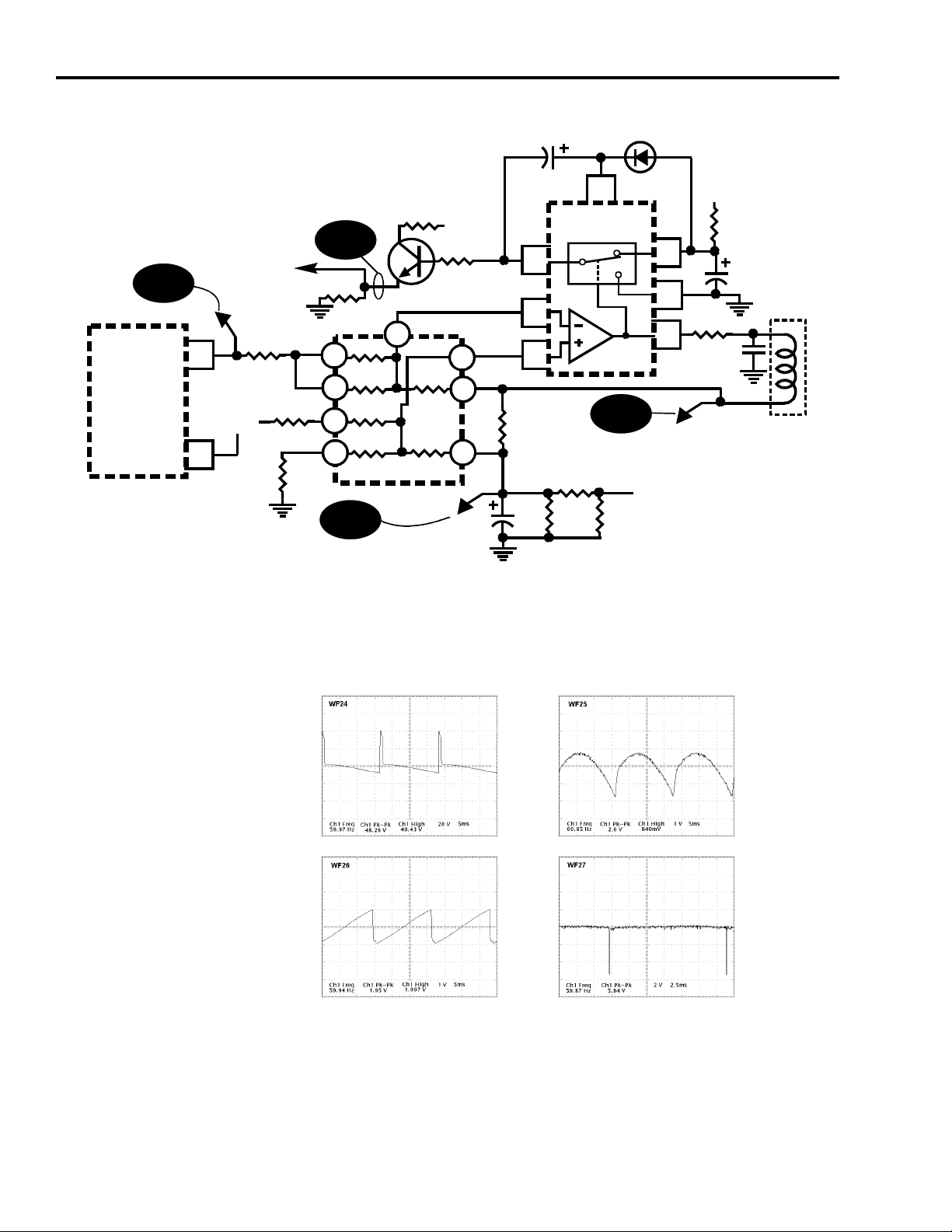
44 Vertical
WF26
WFXX
Vert
Out
T-Chip
Y/C
Deflection
U16201
Vert
VCC
6
7
R14517
U14501
Vert Out
2
4
5
WF24
TP14501
+13V
1/2 Supply
R14515
V-Sync to
U13101-34
15
+7.5
26
R14509
SysCtl
TP14502
R14508
WF27
2
1
7
8
WF25
+13V
3
Q14501
V-Sync
1
3
6
4
R14519
5
RN4501
TP14504
C14502
R14518
Figure 5-1, (Repeated), Vertical Deflection Circuit
+26V
1.5
R14507
Vert
Yoke
Figure 5-4, Vertical Circuit Waveforms
Page 45

Troubleshooting
The vertical circuit is direct DC coupled and does not rely on capacitors for Sshaping and feedback. As a result, vertical troubleshooting can be accomplished
with a digital volt meter and an oscilloscope.
Warning: Do not try to check the DC operation of U14501 by grounding
pin 1 or applying 26 volts. Damage to U14501 or any of the direct coupled
stages may result.
No Vertical Deflection
1. Check for the presence of the 26 volt supply on pin 6 of U14501. If it is not
present, suspect R14511 being open, possibly as the result of a shorted
U14501. If it is correct, go to the next step.
2. Check for the half supply of approximately 13 volts at TP14501 (vertical
yoke connector). If it is not there, check for an open R14519 or R14517. If it
is there, go to the next step.
3. Check for a 2 Vp-p vertical parabola on pin 1 of U14501. If it is not there,
check pin 15 of U16201 for a 2 Vp-p vertical ramp signal. If the ramp signal
is present, suspect a defective U14501. If it is not present, go to the next step.
Vertical 45
4. Check for 7.62 volts on pin 26 of U16201. If it is not there, troubleshoot the
main power supply. If the voltage is correct, check pin 16 of U16201 for
approximately 3.5 volts. If the voltage is wrong suspect a defective C14501,
C14503 or U16201.
Page 46

46 Vertical
Vertical Yokes (Series)
Vert
Yoke
Drive
R19019
R19007
R19013
R19026
PTV Power Supply PCB
R/G/B Video To
Cathode Drivers
Q15102/107/108
Grid 1 Volt
to Pix Tube
(28.5V)
CR15302
R19008
R19012
CR19010
8
2
3
4
C15302
Part of
Trnsfmr
T19001
Dynamic
Focus
CR19011-20V
R19051
R19020
R19016
1
1/2 U19001
PTV Kine PCB
(Video Line)
+250V
5
+23V
5
6
CR19003
4
1/2 U19001
7
Q15304
SW
+10V
Scan Loss Defeat
R19009
R/G/B Video
From Video
Circuits
TP19001
Q19004
Q19003
C15307
Filament Voltage
IHVT/ T14401-8
(34VP-P)
J19106
6
Q19013
Fil Volt (AC)
to PIX Tube
Heater
CR15305
J15102
77
6
Q15301
Amp
CR15303
30V
Q15302
Buff
+10V
CR15304
Q15305
Q15303
Scan Loss
Sw's
+10V
Figure 5-4, Scan Loss Detect & Shutdown Circuit
Scan Loss Detect & Shutdown Overview
The primary function of the Scan Loss Detect and Shutdown circuit is to detect
loss of scan. This is needed in order to protect the picture tubes and also to
protect the convergence yoke driver circuits in the event of a catastrophic failure
in the deflection circuits. This is accomplished almost instantaneously by the
circuits shown in Fig. 5-4 above. Both the horizontal and vertical are monitored
for "unscheduled" shutdowns failure. Horizontal is monitored by using the
filament heater voltage as an indicator. Vertical is monitored by comparing the
voltage across the vertical yoke to a reference voltage. If and when a failure
occurs two things happen, one: the video drive signals to the picture tubes are
muted and two: the Grid 1 voltage to the tubes are turned off.
Page 47

Scan Loss Detect Operation
The scan loss circuit in CTC195 instantly detects the loss of current in the
vertical deflection yokes and blanks the video. This is necessary to prevent
damage to the phosphor on the picture tube by the extreme energy of an undeflected
electron beam. The circuit in Figure 5-4 directly monitors the vertical yoke
current and provides various methods of removing the vertical yoke drive.
In previous PTV chassis the horizontal scan loss was measured indirectly. It was
measured by detecting the picture tube filament pulse. The filament pulse is
obtained from a separate winding on the flyback transformer that is coupled to
the winding that drives the horizontal yoke. Using this method there is a
possibility that vertical yoke scan current could be lost and its loss may not be
detected quickly enough to prevent damage.
The CTC195 detects horizontal yoke current by means of the dynamic focus
transformer T19001. The dynamic focus transformer is a current transformer
with the horizontal yoke current flowing in the primary (not shown). A small
secondary winding (pins 4-5) generates a voltage signal whenever the horizontal
yoke current is present. This signal is peak detected by CR19003 and filtered to
provide drive for transistor switch Q19003. Q19003 forms a logical AND with
vertical scan loss detection transistor (Q19004). With these two transistors on,
ground is appled to the base of Q15305 keeping it off
Vertical 47
The three vertical deflection yokes are wired in series. Two inputs provide the
connection back to the chassis. One side is connected to the vertical amplifier
output. The other side connects to ground through a current sensing resistor
(R19019). If vertical scan is lost, the scan loss comparator circuit (U19001-7)
outputs a Lo to the base of Q19004, allowing it to turn off. When Q19004 turns
off the ground is removed from the base of Q15305 and the pull-up B+ turns it
on. This in turn causes the video and Grid 1 voltage to be shutdown.
Vertical scan loss occurs when one or more vertical deflection yokes are unplugged or an open occurs due to the breaking of the series connection. When
the open occurs, it is important that the video is blanked quickly. Ideally
blanking would occur instantly when the next vertical scan is missed. In the
circuit the differential amplifier (U19001-1,2,3) amplifies the voltage across the
vertical sense resistor (R19019). The negative half of the output signal is clipped
because the negative power pin of the opamp is grounded and the amplifier
output can not go below ground. The output of amplifier (U19001-1,2,3) is a 2
volt peak sawtooth shaped pulse repeated at a 60 Hz rate. This pulse is applied to
the non-inverting input of integrating amplifier (U19001-5,6,7). The inverting
input of amplifier (U19001-5,6,7) is biased at approximately 1 volt. When ever
the non-inverting input exceeds 1 volt, once per vertical cycle, pin 7 integrates
positive (outputs a Hi). The integrating time constant is chosen to keep the worst
case minimum ripple voltage on pin 7 slightly above 1.2 volts when the integrator is pulsed at a 60Hz rate. Whenever pin 7 of U19001 is above approximately
1.2 volts, transistor Q19004 is turned on and if the horizontal detector Q19003 is
also on, video and Grid 1 voltage are enabled.
Page 48

48 Vertical
If vertical yoke current stops, there is no pulse signal to refresh the integrator
and pin 7 quickly falls below 1.2 volts and turns the video off. A feature of this
circuit is that it uses no electrolytic capacitors. Electrolytic capacitors deteriorate in value with heat and time. They are suitable for power filtering but not for
critical timing applications.
Previous projection TV’s detected vertical scan by measuring the AC voltage on
the “S” capacitor located on the main chassis. This is adequate to detect an open
of both inputs but fails to detect a problem with only the “S” cap and/or ground
end of the yoke string (J19101-3). This type of failure could occur because of a
fault with the “S” Cap and/or the ground path opens up in the feedback loop of
the vertical amplifier and the vertical output at the top of the series yoke string.
If this type of failure occurs a 60Hz 26V p-p square wave is passed through the
yokes to the AC scan loss detector and is interpreted incorrectly as a valid
vertical scan signal. A similar failure can occur but for a different reason.
Previously, only a current sense resistor (R19019) and a differential amplifier
(U19001-1,2,3) to produce a voltage that is proportional to the vertical yoke
current. If the feedback portion of the circuit opens, a 26 volt square wave
appears at the input of the op-amp (U19001-2). Ideally, the signal should be
rejected by the amplifier, however this doesn’t happen because of the high
impedance input characteristics, the amplifier can’t reject such a large signal.
The solution to this problem is to use a peak detector consisting of CR19010 and
zener diode CR19011. This circuit detects the loss of the “proper vertical
feedback” signal. During normal operation the voltage on the “S” cap (ground
side…J19101-3) has a 3VAC (60Hz) riding on 13VDC. The feedback loss
detector has a 20 volt zener diode (CR19011) between its peak detector CR19010
and its output transistor Q19013. In normal operation the output transistor
Q19013 is off. When the feedback loss detector sees the 26V p-p square wave
signal which in turn is rectified and filtered to provide approximately 26VDC.
This is enough to cause the zener CR19011 to conduct so that transistor Q19013
is turned on. The output transistor Q19013 turns On and transistor Q19003 turns
Off. This allows Q15305 to turn on shutting down video the Grid 1 voltage.
Page 49

Vertical 49
Vertical Yokes (Series)
Vert
Yoke
Drive
R19019
R19007
R19013
R19026
R19012
PTV Power Supply PCB
R/G/B Video To
Cathode Drivers
Q15102/107/108
Grid 1 Volt
to Pix Tube
(28.5V)
CR15302
CR19010
R19008
8
2
3
4
C15302
Part of
Trnsfmr
T19001
Dynamic
Focus
CR19011-20V
R19051
R19020
R19016
1
1/2 U19001
PTV Kine PCB
(Video Line)
+250V
+23V
5
6
5
CR19003
4
1/2 U19001
7
Q15304
SW
+10V
Scan Loss Defeat
R19009
R/G/B Video
From Video
Circuits
TP19001
Q19004
Q19003
C15307
Filament Voltage
IHVT/ T14401-8
(34VP-P)
J19106
6
Q19013
Fil Volt (AC)
to PIX Tube
Heater
CR15305
J15102
77
6
Q15301
Amp
CR15303
30V
Q15302
Buff
+10V
CR15304
Q15305
Q15303
Scan Loss
Sw's
+10V
Figure 5-4 (Repeated), Scan Loss Detect & Shutdown Circuit
Page 50

50 System Control
System Control
Overview
The CTC195/197 chassis is a digitally controlled television receiver. The system
control circuit governs the entire operation of the television. The control circuits are not
only responsible for turning the set on and off, but also for aligning the different circuits
such as deflection and signal. Adjustments that were aligned with a potentiometer on
other chassis are now aligned digitally via the microprocessor with the values stored in
the EEPROM (Electrically Erasable Programmable Read Only Memory). This means
the values stored may be changed by invoking the correct parameters for the EEPROM
to allow writing to it, then writing the new values. The EEPROM will hold all values
written to it even during and after loss of power. The EEPROM also stores certain user
settings. This ensures that these settings will not be lost during long power outages.
The CTC197 Control System is based on a single 8-bit ST9296 Microcomputer. The
micro has several new features over others used in the past. The new features include
an IR Preprocessor, Sync Presence Detector, Frequency Multiplier for the CPU
Clock, a UART, a Closed Captioning Decoder that can run without H and V from
Deflection (needed for TV Guide Plus+), 3 A/D inputs and an On-Screen-Display that
supports 3-bit D/A outputs (also needed for TV Guide Plus+).
The three I²C busses communicate with the majority of the digital devices. The three
busses are called the Standby, Run and GemStar (TV Guide Plus+) bus. The standby
bus is connected to the main EEPROM and the decoder interface microcomputer,
when present. The run bus is connected to the remainder of the I²C devices. The TV
Guide Plus+ bus will be connected to the TV Guide Plus+ module only. The Standby
and Run busses run at approximately 50 KHz while the TV Guide Plus+ bus runs at
about 100 KHz and will use clock stretching. The TV Guide Plus+ bus runs faster than
the main bus because full screens of display data are sent over the bus from the module
to the main chassis microprocessor. The standby bus is always active, while the run bus
is only active after power up. The TV Guide Plus+ bus can be activated via software
control without powering up the remainder of the chassis. This is to allow updates to
the TV Guide Plus+ material at any time via downloads from the source station.
The CTC195 chassis uses the same main chassis as the CTC197. However, additional
circuitry for PTV (Projection TeleVision) operations are added. These include; digital
convergence, higher power audio amplifiers, an additional power supply and various
CRT control circuitry. I²C bus control is provided for all circuitry.
The CTC197 main chassis devices that are controlled by the I²C bus are the main
EEPROM (U13102), Main Tuner PLL (U17501), Stereo Decoder (U11600), T4 Chip
(U16201), Audio Compressor (11501) and the Video Switch (U26901). Other
devices include the PIP EEPROM (U27903), PIP DAC (U27902), PIP PLL (U17401),
and FPIP (U18100). The optional TV Guide Plus+ module is also controlled via a
dedicated I²C bus. The CTC195 chassis has a Digital Convergence/Convergence
Power Supply board, and an Audio Board with I2C bus controlled devices. The Digital
Convergence microcontroller (U19501) and EEPROM are on a dedicated I2C bus.
Page 51

System Control 51
+12V
STBY
+12V
Gem
Star
PCB
Pwr Loss Mon
Q13501/503
+12V
21
+3.3V
6/14/22/32/40
U18100
Supply
1/2
U14701
& U27905
6
Out
3
4
+5V Run
+12V Run2
+16V Stby
Audio
Compress
U11501
D In
FPIP
D Out
Power
Reg
C
Out
27
28
26
7
3/5
13
14
37
38
39
51
17
D
C
+5V
19
Run/Stby
GemStar
GemStar
System
Control
U13101
Reset
15 Sec
Timer
12
11
Main
EEPROM
U13102
Stby
Data
Stby
Clk
ATE
EN
Run
Data
Run
Clk
PIP EEPROM
U27903
21
C
20
D
(CTC195 Only)
8
D
C
23
24
5
4
3
56
DC
Digi-Con
Micro
IC19501
+5v
28
Decoder
5
6
8
D
19
21
C
J13003
1
"Chipper Check"
6
D
3
C
4
9
Video
Switch
U26901
+5V
Interface
ROM
U23901
ATE
Service
Connector
PIP
DAC
U27902
1
+12V
D
2
4
C
+9.5v
9
10
+7.5V
44
43
19
18
+33V
19
18
D
Decoder
C
U11600
D
C
D
U17401
C
4
4
D
C
22
Stereo
20
3
T-Chip
U16201
PIP
PLL
9
9
Main
Tuner
PLL
U17501
+5V
"PTV ONLY"
19
C
D
18
6
5
Digi-Con
C
EEPROM
D
(CTC195 Only)
Figure 6-1, System Control Block Diagram
Page 52

52 System Control
Standby/AC Line Dropout Detector and Reset
The reset circuitry of the microprocessor monitors the standby +5 and +16 volt
supplies and warns the micro when a power failure may be occurring. Standby, when
used in this application, means that the supply is always on as long as the AC cord is
plugged in. These supplies are available at all times. This contrasts with the Run
supplies, which can only supply power when turned on by the micro. Pin 51 of U3101,
the main microprocessor, is normally held hi by the presence of the +5 Volt standby
power supply voltage. A simple voltage divider network consisting of R13504,
R13505, R13507 and R13510 keeps pin 51 high as long as there is +5 volts coming
from the standby supply. Q13503 is normally biased off when the standby +16V
supply is present. When the standby +16V supply drops to about +7.5V, Q13501
turns on which turns on Q13503 applying a LO to pin 51 of U13101. When this
occurs, the microprocessor disconnects the busses internally and proceeds to go into a
backup routine.
Reset, Recovery, Initialization and BrownOut
The reset circuitry of the control microcomputer monitors the +16V Standby Supply
and resets the microcomputer when the supply drops below roughly 6 volts, making
reliable operation of the microcomputer impossible. With the micro in reset, all the
local controls and the IR inputs are disabled. The RUN/STBY line will be switched to
low removing power to the T4 Chip and all Run regulators.
Software detection
The +16V standby supply is monitored by the microcomputer using an A/D to
determine if a reset condition is imminent, or brownout conditions are present. As the
+16V supply begins to drop, at approximately 12 volts, the micro will turn off the run
supplies and activate the “batten-down-the hatches” routine to save off chassis
operational conditions such as;
1) Current time
2) Current channel
3) On/Off state
4) Input source (Aux/SVideo)
5) Volume Setting
+16V Standby
The +16V Standby supply input is sampled directly by the micro on pin 39 via a 6-bit
A/D. This is used to verify that the supply is active and within regulation. Failure to
meet the level specification will result in a power cycle of the entire instrument using the
“batten down the hatches” routine which will save off the appropriate error code in the
EEPROM. In addition, this input is monitored to control the reset of the main micro
and provide a sense level for the TV Guide Plus+ module low power monitor. The
+16V power supply is designed not to allow a sag of <12 volts to occur. Any drop to
less than 12 volts will cause the micro to run through “batten down the hatches”.
Page 53

System Control 53
15 Second Timer
Once a shutdown condition occurs, a 15 second timer begins its countdown. This
circuit is shown in Figure 6-2 and are the components connected to pin 17. It assures
that the time-of-day is maintained until the timer input on pin 17 of the micro fails to
maintain a logic 1 condition. As indicated by the pin title, this normally happens about
15 seconds after a power failure. This enables the chassis to maintain the time-of-day
through minor power outages or brownouts that may dip below the minimum AC
supply tolerance for less than 15 seconds.
POR ( Power Off Reset)
Circuitry in the T4 chip detects when the standby-power voltage has dropped too low
and shuts off deflection, effectively shutting down the set. The output of the PORdetector is latched and may be read as a status bit over the serial bus by the
microcomputer. This POR latch is reset on the OFF-to-ON transition of the ON/OFF
control bit in the T-Chip. Therefore, if the detector is latched when the TV is ON, it is
necessary to send an OFF command followed by an ON command in order to again
start the instrument. If the standby voltage is still too low when the ON command is
received, the IC will stay in the OFF mode, and the process must be repeated.
3
Power
Supply
Reg
U14701
Out
6
+12V
5
Out
+5V
IR
RX
Run/Stby
19
1
2
+16V
Stby
7
System
Control
U13101
+5V Run
37
+12V Run2
38
39
+16V Stby
IR
36
IN
R13175
FSW
WF28
B OSD
G OSD
R OSD
Reset
15 Sec
Timer
17
R3309
25
C3308
26
27
28
51
C13144
L3101
C3303
To U16201-36
To U16201-35
WF05
Typical
+5V Stby
C13504
Q13503
R2701
R3190
NOTE:
& Green Circuit
Same as Red
+7.5V
Q12701
Q13501
To
U16201-33
Blue
To
U16201-34
TP12701
+16V
Stby
Figure 6-2, System Control Reset
Page 54

54 System Control
User Settings
During shutdown, all current user settings will be stored in EEPROM. Most
settings now are written to the EEPROM as they are changed, with no shadowing
of the EEPROM in RAM. It is no longer necessary to guarantee RAM retention
with this system configuration. The microprocessor has approximately 10ms to
allow any writes to the EEPROM in order to store the present condition of the TV.
EEPROM and T4 Chip Power Control
The microprocessor controls the power to the EEPROM (U13102) and T4-Chip
(U16201). After the microprocessor is reset, U13101 pin 20 goes LO turning on
Q13109. This supplies +5V to the EEPROM (U13102). The T4 Chip uses a +7.5
volt supply derived from the +12 Volt Run supply. A simple voltage divider
reduces the 12 volt to 7.5 volts. Although the 7.5 volt supply is labeled "Standby"
16V Standby
Internal Reset
(Micro)
Micro Internal Res et Active
0
0
Micro Wakes Up
Run/Standby
Speaker Mute
EEPROM Enable
Clock Speed
0
0
16 MHz
4 MHz
0
T0 T1 T2 T3 T4
Wait for Micro
to wake up
Wait for EEPROM
write to finish
EEPROM Disabled EEPROM Re-enabled Wait for 16MHz
clock to stabilize
Figure 6-3, Micro Reset Sequence
in the service literature, it is actually not active at all times. +7.6V to the T4 Chip
is available only when the run +12V supply comes up. The power control circuitry
of the microprocessor gives it the ability to turn off the power to the EEPROM and
T4 Chip in the event one of the devices locks up. Because the micro goes through a
power up sequence every time the instrument is turned on, the T4 Chip and
EEPROM are turned off and then back on each time the TV is turned on. This
resets the EEPROM and T4 Chip each time the TV is powered up.
Main Power Supply On/Off Control
The CTC195/197 chassis are turned on and off by controlling the main power
supply and the T4-Chip. When the power cord is first connected to AC, standby
supplies come up, Q13503 resets the micro by sending a HI to pin 51. Pin 20 then
goes HI applying power to the EEPROM. The microprocessor then checks the
EEPROM address for an acknowledgment. If the EEPROM is acknowledged, the
microprocessor waits for the next command. If there is no EEPROM
acknowledgment, the microprocessor continues to try to contact the EEPROM.
This can be seen on the oscilloscope as continuous data activity on the I2C data
line.
Page 55

Run/Stby
+12 V Run
+5.6 V Run
T-Chip Off/On
Video Blanking
Initialize IC's
Speaker Mute
Degaussing
Vertical Kill
OSD
Tuning
HiFi Line Mute
+16 V Standby
Supply
System Control 55
T0 T1 T2 T3 T4 T5 T6 T7
Figure 6-4, Micro Power Up Sequence
The timing diagram in Figure 6-4, while not being a good troubleshooting tool, can
be a useful learning tool if understood by the technician. Refer to it during the next
section.
With AC power already applied to the set, when the power button is pressed or a
remote control ON command is received, pin 20 goes momentarily LO resetting the
EEPROM. This makes certain it is a normal state. Immediately the +16 Volt Standby
Supply dips. This can be seen at the bottom of the chart during time periods T0-T2.
During this time, the video and audio mute lines are low so that no picture or sound can
be processed accidently by circuitry having some residual voltage supply remaining.
During time T0 the Run/Standby signal at pin 19 goes HI activating the +12 and +5.1
volt run supplies. These supplies ramp up during the remainder of T0 and T1. When
the +12 volt supply reaches about 90%, the micro assumes that the +7.5 volt supply
derived from it is stable enough to activate the T4 Chip which begins starting the
deflection circuits. After this, there is a short amount of time for the Run supplies to
completely stabilize before the I²C devices are initialized. This is also the time when
auto-detect is looking for features on the instrument and continues through time T4-T6.
When IC initialization begins, the micro also stops vertical deflection and degausses the
CRT.
Note that the Hi-Fi and Line outputs are muted normally and held in a non-muted state.
This is so that any power supply drop out will cause the line outputs to mute, reducing
the risk to high-power amplifiers that may be connected to them.
By the end of T6, circuit stability has been established. The OSD and tuner are allowed
to function. As soon as a channel is captured, the video blanking is turned off allowing
video to pass normally. When the high voltage supplies have reached their normal
operating voltages, a picture will appear on the CRT.
Page 56

56 System Control
Video Blanking
T4-Chip
Run/Standby
Speaker Mute
Volume Ramp
12 Volt Run
5 Volt Run
0
1
1
0
1
1
1
T0 T1 T2 T3 T4
Figure 6-5, Micro Power Down Sequence
Power Down
Figure 6-5 shows the normal power down sequence for the CTC195/197 chassis.
Again, this will not greatly aid in troubleshooting, but only in the technicians understanding
of what is happening during a normal power off event. It is always advantageous to
understand what is happening, before being able to pinpoint what is not happening.
The exact time frame involved is unimportant, only the sequence. When either the
power button is pressed or a remote control OFF command is received, the micro
immediately mutes the video. The volume level is reduced, then the speakers are muted
and the T4 chip is ordered to stop deflection. This all happens between T0 and shortly
into T2. During the remainder of T2 and T3, high voltage and deflection are shutting
down. At the beginning of T4 Run/Standby (pin 19 of U3101) is turned to Standby,
shutting down the 5 and 12 volt run supplies, shutting down the instrument.
Batten Down the Hatches
The batten down sequence is one of the most important for the technician to understand.
This is invoked during any problem sensed by the microprocessor and acts to save off
all settings and alignments, plus an error code to cue the technician as to the possible
cause of the failure. It's most important function is to shut down the set as normally as
possible during loss of incoming AC, whether long term or short term.
The batten down sequence will occur when the standby 16 volt supply drops to about
+9.5 volts during a power up cycle, or to about 2 volts below the reading of the standby
D/A on pin 39 of the microprocessor, U3101 1.5 seconds after power up or 1.5
seconds after power down.
Some power supply dip or surge is expected during start up and shut down, so 1.5
seconds was chosen to make certain any ringing or dipping of the supply had stabilized
before taking a reading that might lead to a batten down sequence, when the only thing
occurring was a normal power supply dip or surge during start-up or shut down.
Page 57

System Control 57
Figure 6-6 shows the timing during a typical batten down sequence. The "Power Fatal"
trigger is the +16 volt standby supply monitor on pin 39 of the microprocessor, U3101.
Anytime after the 1.5 second power on cycle, if the 16 volt standby supply falls below
approximately 9.5 volts the batten down sequence begins. The first actions are to
jettison all devices the drain the residual power supply. The speaker outputs, run
supplies, OSD display, Star Sight and any other circuit not necessary to saving
information to the EEPROM are cut loose. All instrument information is written to the
EEPROM during the next 10 milliseconds. After that, the EEPROM is disabled by pin
20 of the micro going HI. When this sequence is completed, two things may happen
depending upon the condition of the standby supply. The 15 second timer on pin 17
tells the micro how long the power has been disconnected. If it has been less than 15
seconds, the set is powered up with no loss of data, including the clock time. If it has
been greater than 15 seconds, the clock time is lost. When the EEPROM has stabilized
after T4, one more write containing device status after the batten down the hatches
routine started is written.
The microprocessor continuously monitors the +5 and +12 volt run supplies and can
write an error code when it detects the failure of either. This might not be extremely
valuable considering the set will not run without both supplies working. However, if
either supply drops out longer than 500 milliseconds, an error code will be logged. See
the error code list for the code explanations.
Power Fatal
(pin 39)
Speaker Mute
(Pin 50)
Run/Standby
(Pin 19)
OSD PLL
SS Low Power
(Pin 11)
SS Reset
(Pin 9)
EEPROM Disable
(Pin 20)
T0 T1 T2 T3 T4
2.3 mSec
10 mSec wait for
EEPROM writes to
finish
30 mSec EEPROM disabled
Figure 6-6, Micro Batten Down the Hatches Sequence
10 mSec wait for
EEPROM supply
to stabilize
Page 58

58 System Control
Feature Auto Detection
As with the CTC179/189, certain features of the CTC195/197 chassis family are auto
detected. The microprocessor checks for the appropriate hardware and if detected,
supports that feature. If not, it assumes that feature is not supported in the chassis and
runs without it. In these instances, the set will not shutdown, but will run minus the
feature. One example is the digital convergence board for the CTC195 projection sets.
If the convergence board is disconnected or malfunctioning, the micro will not receive
an acknowledgment and revert to a direct TV mode. Currently auto-detected features
include; TV Guide Plus+, MCR (Commercial Chassis), Digital Convergence on PTV's,
and 2 Tuner PIP.
Run Supply Detector
As previously discussed, the system control circuitry monitors the +5 and +12V run
supply directly from inputs to pins 37 and 38, once the set has been turned on. If for
any reason the run supply is not present when the set is initially turned on, the
microprocessor will abort the power on sequence and then try to restart the set. If
after three tries the run supply is not detected, the microprocessor places the TV in the
off mode. This is known as the "three strikes and your out" sequence. Pressing the
power button will restart the detection process. Remember there are only three error
code locations and that every start attempt will fill one of the locations. If the set is
restarted, the new error codes will overwrite the ones recorded during the previous
power up attempt.
The +16 volt supply is also directly monitored by pin 39 of the microprocessor. After
the 1.5 second delay at start up for the supply sag to recover, system control begins to
monitor the supply. If at any time the normal operating voltage drops farther than 2
volts, the micro will enter the batten down sequence.
A loss of horizontal deflection may cause the run supply detector to trip. Without
the load of the horizontal deflection circuitry, the 140 volt B+ starts to climb. The
power supply error amplifier, which monitors the +140 volt line for regulation,
shortens the duty cycle of the power supply to reduce the B+. However, the +12
volt supply is still fully loaded and consequently may slump to less than the required
voltage the microprocessor is looking for, causing the run detector to trip. This will
cause the microprocessor to log a run supply error code. In some cases, the +5
volt supply may also exhibit the same problem, but the +12 volt supply would be the
most likely suspect.
Page 59
System Control 59
Microprocessor Input Signals
Certain video and deflection signals are input to U13101. Selected video out is
buffered by Q13306 and applied to pin 13 for the closed caption decoder contained
within U13101. Video out of the T4 Chip is buffered by Q13101 and applied to pin 38
for tuning sync (see tuning algorithms for more information). Horizontal and vertical
deflection pulses are applied to U13101 pins 24 and 25 respectively to provide a
synchronization reference for correct positioning of the on screen display.
Microprocessor Pin Assignments
Understanding the role of the microprocessor in the operation of the instrument will
greatly assist the technician in any troubleshooting. Many of the outputs and inputs of
the micro are digital, which means they are either a logic 0 or 1. They can be measured
with a standard DVM as either a HI (2.5–5.0 volts) or a LO (< 2.5 volts). Activity on
data and clocks can be seen as in Figures 6-7 and 6-8. On an oscilloscope very little
detail can be distinguished, but the presence of activity is generally all that is needed to
be known. If the clock line is flat, there is probably micro trouble. If the data line is flat,
it first must be understood what communication should be taking place before assuming
that no activity means a defect.
Figure 6-7, Data Line Activity
Figure 6-8, Clock Line Activity
Page 60

60 System Control
Figure 6-9, U13101
Microprocessor Pinout
O
1
IF VC1
O
2
IF VC2
O
3
RUN I2C CLOCK
I/O
4
RUN I2C DATA
I/O
KD1/ATE ENABLE
5
I
6
KS1
I
KS2
7
I
8
KS3
O
PAL 50/60 HZ
9
I
2ND TUNER AFT
10
O
GEM LOW POWER
11
O
DI RESET
12
I/O
13
GEM I2C DATA
O
GEM I2C CLOCK
14
I
15
CC VIDEO
I
16
VDD2
I/O
15 SECOND TIMER
17
I
2ND TUNER SYNC
18
O
RUN/STANDBY
19
O
EEPROM ENABLE
20
I
MAIN TUNER H
21
I/O
DI BUS ENABLE
22
I/O
STANDBY I2C DATA
23
O
STANDBY I2C CLOCK
24
O
FAST SWITCH
25
O
BLUE OSD
26
O
GREEN OSD
27
O
RED OSD
28
U3101
FM STEREO
FM TUNED
DATA OUT
DATA IN
RESET I
RESET
SPEAKER MUTE
SVM
AVR
TILT D/A
SRS NORM/EN
DEGAUSS
CONTROL #2
CONTROL #1
OSC IN
VSS2
OSC OUT
+16 VOLT STANDBY A/D
+12 VOLT RUN A/D
+5 VOLT RUN A/D
HORIZ SYNC
VERT SYNC
FILTER OSD
VDDA
FILTER CPU
VSS1
VDD1
I
56
I
55
I/O
54
I/O
53
I
52
I
51
O
50
O
49
I
48
O
47
I/O
46
O
45
44
O
43
O
42
I
41
I
40
O
39
I
38
I
37
I
36
I
IR
35
I
34
I
33
I
32
I
31
I
I
30
I
29
U13101 Pin Functions:
The accompanying diagram describes the functions of the microprocessor, U3101.
The function is outlined briefly and whether the pin is an output, input, both, or power
supply or ground.
1. IF VC1: The IF_VC1 output of the microcomputer is an integrated pulse width
modulated digital to analog converter signal used to control the alignment of the IF
output stage of the main tuner. D/A Output.
2. IF VC2: The IF_VC2 output of the microcomputer is an integrated pulse width
modulated digital to analog converter signal used to control the alignment of the IF
output stage of the main tuner. D/A Output.
3. Run I2C CLOCK: The Run I²C CLK line is an output line which conforms to the
Philips I2C Bus Specification. The maximum clock rate is 100kHz. The Run I²C CLK
line is operational only when the receiver is in “Run” mode (Run mode is defined as
either the TV is on, the TV Guide+ timed download is active or the Decoder Interface
download is active).
Page 61

System Control 61
4. Run I2C DATA: The Run I²C Data line is an I/O line, which conforms to the Philips
I²C Bus Specification. The Run I²C CLK line is operational only when the receiver is in
“Run” mode (Run mode is defined as either the TV is on, the TV Guide Plus+ timed
download is active or the Decoder Interface download is active) .
5. KD1/ATE ENABLE: The KD1 line is configured as an output that switches
between logic 0 and 1 levels to detect key presses from the front panel assembly.
Following a Reset, the ATE_EN pin is read to determine if ATE mode has been
selected. ATE mode is enabled if the input is >3.78V, normal user mode is selected if
the line is <1.38V.
6. KS1: The KS1 line is one of three lines (KS1, KS2, KS3) configured as inputs to
detect front panel key presses. The lines are normally high (5V) and are pulled to
ground by a key closure.
7. KS2: The KS2 line is one of three lines (KS1, KS2, KS3) configured as inputs to
detect key presses. The lines are normally high (5V) and are pulled to ground by a key
closure.
8. KS3: The KS3 line is one of three lines (KS1, KS2, KS3) configured as inputs to
detect key presses. The lines are normally high (5V) and are pulled to ground by a key
closure.
9. PAL 50/60 HZ: The PAL_50/60HZ output line is used to control the mode of a
PAL module, when installed. A logic 1 indicates 50HZ mode.
10. 2ND TUNER AFT: The 2nd Tuner AFT is an input from the 2nd tuner IF. It is the
output of a comparator whose input is controlled by a bus controlled D/A IC. The 2nd
tuner AFT signal is used during channel tuning to determine the presence of AFT
crossover. The Channel Tuning for the 2nd tuner is controlled by the main micro.
Logic 1>3.8V, Logic 0<1.0V
11. GEM_LOW POWER: The TV Guide Plus+ Low Power Mode input is used to
tell the TV Guide Plus+ micro that the +5V supply used by the TV Guide Plus+ micro
will drop out within 50 msec. The TV Guide Plus+ micro will then properly power
down.
12. DI RESET: The DI Bus Reset is not used.
13. GEM_I2C DATA: The GEM I²C DATA line is an I/O line, which conforms to the
Philips I2C Bus Specification. The maximum clock rate is 100kHz. The GEM I²C Data
line is operational as long as the receiver is plugged in.
14. GEM_I2C_CLK: The GEM I²C CLK line is an output line, which conforms to the
Philips I2C Bus Specification. The maximum clock rate is 100kHz. The GEM_I²C_CLK
line is operational as long as the receiver is plugged in.
15. CC Video: CC Video is an input to the control system. The line contains 1.0Vpp (negative going sync) NTSC video. This is used to provide the Closed Caption signal
to the microprocessor for decoding into usable text.
CC Video input level 1.0Vp-p +/-.2V (from 100 IRE to -40 IRE sync tip)
Page 62

62 System Control
DC Level 2.5V nominal
16. VDD2: The microcomputer and EEPROM use the +5V_STBY1.
Input Level 5.0V +/-8%
Current Requirement 5mA min (Standby Mode), 70mA max (Run Mode)
Ripple 100mVp-p max.
17. 15 Second Timer: The 15 second timer determines whether time-of-day clock
information is discarded after a power dropout. If a dropout lasts longer than 15
seconds, the time-of-day information will be cleared. If it is less than 15 seconds, it will
be retained.
18. 2ND TUNER SYNC: The 2ND_TUN_SYNC input is horizontal sync from the
2nd tuner. The separated sync is sampled by the micro to determine the presence of
valid video during channel tuning.
Logic 1>3.8V (Sync active high), Logic 0 <1V
19. RUN/STANDBY: The RUN/STBY is a buffered output line used to turn on the
Run supplies. Run Mode is selected when the output is a logic 1.
Logic 1>3.5V, Logic 0 <.6V
20. EEPROM ENABLE: The EEPROM ENABLE output is used to control the
standby supplies going to the EEPROM. This line allows the EEPROM to be reset in
the event of an SCR latch.
21. MAIN TUNER H: The Main Tuner Low-Passed Video or "Main Tuner H" input
is baseband video (negative going sync) from the main tuner which will be separated by
a control system sync separator. The separated sync is sampled by the micro to
determine the presence of valid video during channel tuning.
Input Video 1Vp-p (sync tip to 100IRE white)
22. DI BUS ENABLE: The DI Bus Enable is not used.
23. STANDBY I2C DATA: The STBY I²C Data line is an I/O line, which conforms to
the Philips I2C Bus Specification. The maximum clock rate is 100kHz. The standby
I²C Data line is operational as long as the receiver is plugged in.
24. STANDBY I2C CLOCK: The STBY I²C CLK line is an output line, which
conforms to the Philips I2C Bus Specification. The maximum clock rate is 100kHz.
The standby I²C CLK line is operational as long as the receiver is plugged in.
25. Fast Switch (FSW): The fast switch line is the output of a 1-bit D/A. The output is
active high when OSD is present.
Logic 1; >2.7V (OSD active), Logic 0; <.4V (OSD not active)
Output Bandwidth 100HZ-7MHZ
26. Blue OSD: The blue on-screen display signal is the output of a 3-bit D/A. The pin
voltage is 1.0Vp-p (100IRE) and is divided down to 0.5Vp-p for roughly (70IRE)
OSD characters. Rise and fall times after the filter are nominally 70nsec.
Page 63

System Control 63
Output Bandwidth 100HZ-7MHZ
27. Green OSD: The green on-screen display signal is the output of a 3-bit D/A. The
pin voltage is 1.0Vp-p (100IRE) and is divided down to 0.5Vp-p for roughly (70IRE)
OSD characters. Rise and fall times after the filter are nominally 70nsec.
Output level 0.5Vp-p (for nominal 70 IRE OSD)
Output Bandwidth 100HZ-7MHZ
28. Red OSD: The red on-screen display signal is the output of a 3-bit D/A. The pin
voltage is 1.0Vp-p (100IRE) and is divided down to 0.5Vp-p for roughly (70IRE)
OSD characters. Rise and fall times after the filter are nominally 70nsec.
Output level 0.5Vp-p (for nominal 70 IRE OSD)
Output Bandwidth 100HZ-7MHZ
29. VDD1: +5V Standby Supply Voltage.
Input Level 5V +/- 8%
Current Requirement 100uA min20mA max
Ripple 100mVp-p max.
30. VSS1: Ground return path
31. Filter CPU: Filter used to keep various unwanted signals from interfering with
microprocessor functions
32. VDDA: +5V Standby Supply Voltage.
Input Level 5V +/- 8%
Current Requirement 100uA min to 20mA max
Ripple 100mVp-p max.
33. Filter OSD: Filter used to keep various unwanted signals from interfering with
microprocessor functions, in this case with OSD.
34. VERTICAL SYNC: The Vertical Sync input signal to the control system is used to
synchronize the OSD signal to vertical. Only the leading edge is used. The Vertical
Sync signal is used to blank the OSD during vertical retrace. An internal delay is used
in the main micro to insure that the leading edges of Vertical and Horizontal do not
overlap. A single value of the internal Vertical delay is intended for all chassis. A spike
filter, which ignores any glitch of < 2usec after an active edge is detected was added to
prevent double vertical pulses on PTV instruments.
Input Level 0-5.2V max DC (active high)
Logic 1 >3.5V (Vertical active)
Logic 0 <1.0V (Vertical not active)
Max variation in edge 32usec relative to video
35. Horiz Sync or "FBP": The FBP input signal to the control system is used to
synchronize the micro OSD to the flyback pulse. Only the leading edge is used. The
width of the Control Horizontal Sync signal derived from the Flyback Pulse is used to
Page 64

64 System Control
blank the OSD during horizontal retrace. The 5V level of the flyback waveform was
chosen to minimize OSD variation with flyback loading.
36. IR: The IR is the infrared input to the microcomputer accepting IR from the
Remote Control IR Receiver. The circuitry allows for a simultaneous 2nd IR receiver
on a separate FPA for use on consoles in addition to an IR input from the Smart Plug
interface which is used on commercial products.
37. +5.1V RUN A/D: The +5.1V Run supply input is sampled by a 6-bit A/D in the
micro and used to verify that the supply is active and within regulation. Failure to meet
the level specification will result in a power cycle of the entire instrument using the
“batten down the hatches” routine which will save off the appropriate error code is the
EEPROM.
Input Level 5.1V +/- 20%
Ripple 100mVp-p max.
38. +12V RUN A/D: The +12V RUN supply input is sampled by a 6-bit A/D in the
micro and used to verify that the supply is active and within regulation. Failure to meet
the level specification will result in a power cycle of the entire instrument using the
“batten down the hatches” routine which will save off the appropriate error code is the
EEPROM.
Input Level 12V +/- 20% (for valid 12V_RUN)
39. +16V STANDBY A/D: The +16V STANDBY supply input is sampled by a 6-bit
A/D in the micro and used to verify that the supply is active and within regulation.
Failure to meet the level specification will result in a power cycle of the entire instrument
using the “batten down the hatches” routine which will save off the appropriate error
code in the EEPROM. In addition, this input is sensed to control the reset of the main
micro and provide a sense level for the TV Guide Plus+ Low Power Monitor. Any
drop to less than 12 volts will cause the micro to run through “batten down the hatches”.
The 16V STBY is also used as a power supply for the TV Guide Plus+ module
Current Requirement @16V: 25mA typical 50mA max. The total TV Guide Plus+
requirement is 50mA typical, 100mA max for both the 5VSTBY and 16VSTBY
supplies.
40. OSC OUT: 4 MHz clock crystal
41. VSS2: Ground return path
42. OSC IN: 4 MHz clock crystal
43. CONTROL 1: The CTRL 1 output line is one of two audio/video control lines.
Logic 1>3.7V, Logic 0<0.4V
44. CONTROL 2: The CTRL 2 output line is one of two audio/video control lines.
Logic 1 >3.7V, Logic 0 <0.4V
45. DEGAUSS: The Degauss signal is a buffered output signal sent to operate the
degauss relay. Once a power-on sequence has been initiated and the power supplies
Page 65

System Control 65
reach a specified voltage, the Degauss line is held low (Degauss active) for approximately
1.5 seconds. Under normal conditions the Degauss line is high. The Degauss buffer
transistor is located in the Deflection area.
46. SRS NORM/EN: The SRS Normal/Enhanced output is used to switch the SRS
mode from normal (active high) or enhanced (active low). The SRS Norm/En line is
also used to auto-detect the SRS feature at power-up. Following a reset, the SRS
Norm/En line will be read as an input to determine if SRS is present. A logic 0 on the
input indicates that SRS is present.
47. TILT D/A: The Tilt_D/A output allows the user to compensate for the affects of the
earth’s magnetic field on the raster alignment. The Tilt D/A will allow a minimum of 64
customer adjustment points.
48. AVR: The AVR line is a digital input to the micro. A logic 1 indicates that the
average power being delivered to the speaker is in excess of the continuous rating of the
speaker. The micro senses this input and reduces the volume at a rate of 3 steps per
100msec until the AVR line is cleared. The micro will then increase the volume at a rate
of 1 step per 100 msec until the AVR line is set or the original volume setting is reached.
49. SVM: The SVM (scan velocity modulation) output is used to control SVM. SVM
will be turned off whenever the Sharpness control is reduced below the specified step.
A logic HI indicates SVM is active. In addition, SVM will be turned off whenever the
OSD is active to prevent ghosting.
50. SPEAKER_MUTE: The Speaker Mute output is used to force the power amp into
a low-power / muted mode.
51. RESET: The Reset is an input to the Control System providing a reference voltage
for sensing the level of the 16 Volt Standby Supply. It is normally 5.6 volts, obtained
from a zener reference used for the +5V STBY1 and +5V STBY2 supplies.
Reference Voltage: 5.6V +/- 8%, Ripple: 100 mV p-p.
52. RESET I Not used for normal instrument operation at this time.
53. DATA_IN: The Data In line is a UART input line to the micro. It will be used by
both the Comphone and MCR modules to communicate to the main micro. Comphone
and MCR are mutually exclusive features.
54. DATA_OUT: The Data Out line is the output from a UART in the micro. It will be
used by the MCR to communicate to the main micro. The Comphone On/Off output
line is used to activate the Comphone feature. A Logic 1 (high) indicates that the
Comphone IC is active. A Logic 0 indicates that the Comphone feature is in lowpower mode. The DATA_OUT line is auto-detected to determine the presence of
either the Comphone or MCR feature.
55. FM_TUNED:
The FM Tuned input is active high when an FM channel is present. The micro uses the
input state to control the tuning and OSD.
56. FM_STEREO: The FM Stereo input is active high a stereo FM channel is
present. The micro uses the input state to control the OSD.
Page 66

66 System Control
IR Input
Infrared remote signals are amplified by IR3401 and appear at U3101 pin 36 as 5 Vpp negative going data pulses. When no IR is received, the DC level at U3101 pin 36 is
5V. IR3401 is powered by the 5V standby supply. There is no power indicator LED
on the normal CTC197 chassis.
OSD Circuit
The CTC195/197 On Screen Display circuit consists of red, green and blue analog
signals from U3101 pins 28, 27 and 26 respectively. These signals along with the FSW
(fast switch) signal from pin 25 are sent to the T4 Chip through buffer transistors
Q12701, Q12703 and Q12702 and input to U16201 pins 34, 35 and 36. These on
screen display signals include the television user menus and also any closed caption
information. The FSW signal is also used by the T4 chip to turn off edge replacement
during the time interval OSD is active, preventing incoming video from appearing in the
OSD.
3
Power
Supply
Reg
U14701
Out
6
+12V
5
Out
+5V
IR
RX
Run/Stby
19
1
2
+16V
Stby
7
System
Control
U13101
37
+5V Run
+12V Run2
38
39
+16V Stby
IR
36
IN
R13175
FSW
WF28
B OSD
G OSD
R OSD
Reset
15 Sec
Timer
17
R3309
25
C3308
26
27
28
51
C13144
L3101
C3303
To U16201-36
To U16201-35
WF05
Typical
+5V Stby
C13504
Q13503
R2701
R3190
NOTE:
& Green Circuit
Same as Red
+7.5V
Q12701
Q13501
To
U16201-33
Blue
To
U16201-34
TP12701
+16V
Stby
Figure 6-10, OSD Output Buffer
Page 67

System Control 67
Service Menu
The CTC195/197 chassis has a more limited built-in service menu than the previous
CTC177/187 and CTC179/189 chassis. Only a few CRT setup alignments and picture
geometry adjustments are provided for internally.
All other alignments must be performed with a computer using Chipper Check™,
TCE's computer-based troubleshooting/alignment software.
To enter the on-board service menu, with the instrument on, press and hold the Menu
button. Then while continuing to hold the Menu button, press and release the Power
button. Then press and release the Volume + button. The instrument should immediately
display a one line menu on the screen. The decimal value on the left is the parameter
number and the decimal value on the right is the current value of that parameter. The
Channel-Up and Channel-Down buttons increment and decrement the parameter
number, while the Volume+ and Volume- buttons adjust the current value of that
parameter. When parameters are modified, the corresponding T4-Chip (or tuner)
registers and EEPROM locations are updated. The Power-On, Power-Off buttons on
the menu, or Power-Toggle button on the front panel exit service mode. The number
below and in the center is the software version number.
P 0 000 V 00
6.03
Figure 6-11, Service Menu Access
P 0 000 V 76
6.03
Page 68

68 System Control
Under normal conditions, a failure of an I2C device will prevent the TV from turning on.
Because a possible reason for needing service is a failed bus IC, the normal check for
acknowledge is disabled in the service mode. If an I2C device has failed, its address
will be stored in the error code area (see next section).
When the service mode is first turned on, the parameter will be 0. This 0 parameter is
used for security purposes to protect the factory alignments from inadvertent modification
by requiring a specific value be selected before other parameters may be accessed. If
channel up is pressed while in parameter 0, the service mode will be exited. One
security parameter must be selected before the service technician proceeds to any of
the main groups. Each parameter group will also have a prefix number displayed
between the P and parameter number used to tell the service technician which set of
parameters he is currently adjusting. To select the security parameter, while in
parameter 0, change the value (using volume up/down) to 76 or 80 for levels 0 or 1
respectively. These will be the only parameters available to the technician from the
front panel of the instrument. All other alignments or adjustments are only accessible
via the Chipper Check™ troubleshooting software and a PC.
Error Codes
Upon certain errors occurring in the chassis, an error code will be stored in the
EEPROM. This error code is displayed to the service technician as the value located at
parameter 0 01, 0 02 and 0 03. If a 0 is stored, there have been no errors. If there is
a nonzero value, however, the following table describes what error occurred. If
multiple errors occur, the first error is stored in 01, the second error is stored in 02 and
the last error to occur is stored in 03. Because only the last error location (03) is
incremented upon each additional error, the error codes should all be reset to 0 upon
completion of the service effort so that a three error code history will be available in the
future. The error code numbers are changed just like the other alignment parameters
If an IC error code is found that is the same as one in the table, then that device did not
acknowledge. For example, if the error code is 128, the Stereo Decoder (U11600)
did not acknowledge. If the error code is the same as any in the table, but incremented
by 1 (129) then the read register did not respond. The problem indicated is still the
Stereo Decoder.
Page 69

System Control 69
Error
Codes
(DEC)
0 All Power OK No Error Codes Thrown
2 All 5V Run Supply Micro 5.1V supply low
3 All 12V Run Supply Micro 12V supply low
8 All XRP U6201 XRP detected by T4
9 All T4 POR U6201 Power On Reset at T4
10 w/FPIP FPIP POR U8100 Power On Reset at FPIP
11 All Stereo Decoder POR U1600 Power On Reset at Stereo Decoder
12 All AVR Latched Micro AVR input to micro held low
16 All I2C Run bus Latched Micro
20 All Software Stack Overflow Micro Note Condition in which Occured
Chassis Error Device Condition
Run I2C cl ock or data line clamped
at logic 0
21 All FPIP/Vid Sw Mismatch Micro
22 A l l 4 Str ike s Your O ut M i c r o
44 w/FPIP FPIP Fault U8100 Failure to r eceive ACK from FPIP
56
64 w/2nd Tuner 2nd Tuner DAC bus fault U7902
102 All w/GemStar GemStar Fault GemStar
103 All w/GemStar GemStar Fault GemStar
128 All Stereo Demodulator U1600
130
134 All Video Matrix U6901
186 All T4 Chip U6201 Failure to receive ACK from T4
196 All Main Tuner PLL U7501
198 All Main Tuner DAC U7501
220
w/Digital
Convergence
w/Audio
Compressor
w/Decoder
Interfa ce
Di gita l C o nv e r ge nc e I 2 C
bus
Audio Compressor U1501
Interface Bus Fault Decoder Module
Vid Sw De tected but FPIP Doesn't
ACK on I2C bus
Code is thrown after 4th
uns uc ce s s f ul t r y to R e - S t art
Fail ure to receive ACK from
Di g ita l C o nv e r ge nc e Mo d ule
Failure to receive ACK from 2nd
Tuner D AC
GemStar module di d not ACK to
Sys Ctl Micr o
GemStar module di d not ACK to
Sys Ctl Micr o
Fail ure to receive ACK from
Stereo Demodulator
Failure to r eceive ACK from Audio
Compressor
Failure to r eceive ACK from Video
Matrix Switch
Failure to r eceive ACK from Main
Tuner P LL
Failure to r eceive ACK from Main
Tuner D AC
Failure of communicaions with
Decoder Interface Micro
Table 6-1, Error Code Table
Page 70

70 System Control
Other error codes may indicate a failure condition some other place in the chassis, such
as the power supply. It is important to understand how these error codes are detected
by the system control circuitry so they can be interpreted correctly and used accordingly.
Most of the error codes are self-explanatory. However some require additional
explanation
There are four power supply error codes – 1, 2, 3 and 4. They monitor the run supplies
for any voltages dipping below a preset level. A detailed explanation of the
microprocessors role in monitoring the power supplies and incoming AC power has
been given in previous discussions.
Unfortunately, any of the above failures will prevent the television from turning on,
making the error codes impossible to read via the service menu. These error codes can
only be checked by reading the EEPROM directly. This can be accomplished by using
the industry’s first color television computer based alignment software called “Chipper
Check™.” Chipper Check™ allows the service technician to perform digital alignments,
read the diagnostic error codes and check the hardware integrity of EEPROM. This
can literally reduce repair time by hours by accelerating the alignment process, preventing
unnecessary parts orders and by giving the technician a means of checking the EEPROM
even when the TV will not turn on. Chipper Check™ is now available. Contact TCE
Publications at (502) 491-8110 for more information.
Error code 4 is a Run Supply Momentary Dropout. This error code is logged when the
microprocessor realizes the power supply turned off for a moment but when checked
500 msec later, it was back on. This is detected by U3101 pin 37 and 38 by monitoring
the +5 and +12 volt run supplies.
Troubleshooting
The system control circuit controls every function of the TV. A failure in this circuit will
cause the entire TV to malfunction. Provided U13101, U13102, and U16201 are
functioning, the set can be forced to turn on in the service mode by holding down the
MENU button and pressing POWER and VOLUME UP in that order. Entering the
service menu and reading the error codes will lead the technician to the defective circuit
area. In some cases, the set will not be able to be forced on even in the service mode.
In these cases, the set will most likely try to start three times and then stop or remain
silent and do nothing at all. When the technician encounters this, the TCE troubleshooting
and alignment software, Chipper Check™, may be used to read the EEPROM error
codes to begin repair efforts.
I²C Bus
When the set is first plugged in, the Standby I²C data and clock lines (U13101 pins 23
& 24) will have about 50 milliseconds of 5 volt p-p data and clock. The pulses are at
approximately 50 kHz. After the initial data and clock activity are sent by the micro,
both the standby data and clock lines should go low and remain.
Before sending out an I²C command, the software checks that the lines are high. If
something is clamping the bus, the software will remove power from the EEPROM for
30 milliseconds and then attempt to send the command again. If the bus worked, the
micro will write an error code (bus latch) to the service menu location.
Page 71

System Control 71
When an attempt is made to turn the set on, the RUN/STANDBY line (U13101 pin 19)
will be set high and the T4 Chip will be toggled off, then an ON command will be sent.
The micro will check the Run Data and Clock lines the same as it did the Standby lines
before attempting to send the command. If the set does not turn on, check the level of
the of the Run Data and Clock lines at the time the RUN/STANDBY pin goes high.
The data line should have information within 40 milliseconds after the RUN/STANDBY
line goes high. If both do not go high, something is loading one of the lines. The micro
should have written the appropriate error code in the service menu location.
Three Strikes and You're Out
This is the term used to describe what the software does following the detection of an
I²C Bus error indicating hardware or software failure. Normally, the micro sends out
commands, then waits for an acknowledgment that the command was received. The
software attempts to re-send any commands when it does not receive that
acknowledgment. If the command is not acknowledged after the second attempt, the
"batten down the hatches" sequence is initiated. "Batten" stores off information to the
EEPROM and then removes power from the instrument. The software will then
attempt to restore power to the instrument. If the error is not corrected, the software
will repeat the "batten down the hatches" routine two more times before shutting the set
off again. The set must then be manually turned on for the "three strikes and you're out"
counter to be reset.
Dead Set - Degauss Relay Clicks
If the television tries to start three times and then stops (you can hear the clicking sound
of the Degauss relay energizing), this means the EEPROM (U13102) and T4 Chip
(U16201) are working (hardware is OK). Therefore the problem is most likely power
supply and/or deflection related. To isolate the fault, perform the following steps.
1. Check the +16 volt standby supply input at pin 39 for proper voltage. Also check
for a HI signal from the RUN/STANDBY pin 19.
2. Confirm proper power supply operation by checking the inputs to pins 37, 38 and
51. These are the +5.1 and +12 Volt Run supply voltages and the micro reset pin.
3. Apply normal AC and confirm that horizontal pulses are momentarily output at pin
22 of U16201, the T4 Chip, when the power button is pressed. If pulses are not
output suspect a defective U16201 or corrupt data in U13102. If pulses are
output, go to the next step.
4. Unsolder the collector of the horizontal output transistor, Q14401.
5. Press the power button so the set attempts to start. Before the third start attempt,
apply an external +16 volt supply to the cathode of CR14107. This will hold up the
+12 volt run supply satisfying the run detector at U13101 pin 38. Once the main
power supply comes up, the external supply can be removed. Confirm horizontal
drive pulses continue to be output at U16201 pin 22. This confirms a horizontal
deflection problem. See page 36 for horizontal deflection troubleshooting
procedures.
Page 72

72 System Control
Dead Set - No Clicking Relay
1. Press the power button and check for U13101 pin 19 to go HI (+5V). If it goes
2. Check U13101 pins 16, 29 and 32 for the +5V standby supply. Check pin 8 of
3. Check the reset signal on U13101 pin 51 for approximately 5 volts. If this pin is
4. Check U13101 pins 40 and 42 for ~ 4.5 Vp-p 4MHz sine-wave (using X10
5. Monitor U13101 pin 23 with an oscilloscope set at 10 msec/div when 120 V.A.C.
HI, check power supply regulator, U14701, and its associated circuitry in the
power supply on/off control circuitry. If they check OK, suspect a power supply
problem. See page 18 for power supply troubleshooting. If U13101 pin 19 does
not go HI, go to the next step.
U13102 for +5V standby supply. Check pins 3 and 20 of U16201 for the +7.6
volt supply. If all the supplies are present, go to the next step. If any of the standby
supplies are missing, check the respective +5V standby supply source and the
EEPROM / T4 Chip power control circuit.
LO, troubleshoot the reset circuitry. If this pin is HI, go to the next step.
probe). If it is not present, suspect a defective Y13101, C13106, C13107,
R13107 or U13101. If the oscillator is present, go to the next step.
is applied to the set. Check for the presence of momentary clock and data pulses
after the data line rises to 5 volts. If the data line goes HI and the pulses appear, go
to step 7.
6. If the data line does not go to +5 volts, unsolder pin 23 of U13101 and see if the
pad goes up to +5V. If it does, U13101 is most likely loading down the bus and is
defective. If it does not go up, check the +5V pull-up supply from R13327 and
check for a device loading down the data line. If the data line goes HI but the
negative going pulses do not appear, unsolder the clock line (U13101- pin 24) and
check for continuous pulses from pin 23. If the pulses do not appear, suspect a
problem with U13101. If the negative going pulses appear when power is first
applied or when the clock line is disconnected, go to the next step.
7. Reconnect the clock line if it was disconnected in the previous step. Press the
power button and look for data activity from the data line, U13101 pin 23. If data
pulses appear when the power button is pressed, go to the next step. If no pulses
appear, suspect a problem with the front panel or the keyboard drive and scan
lines.
8. Check pins 43 and 44 of the T4 Chip to see if the clock and data pulses are
present. If they are present, suspect a problem with U16201 or U13102.
Page 73

System Control 73
No Remote Control
Check for an idle voltage of 5V (logic HI) at pin 36. Press any IR button and check for
a series of 5V p-p pulses at pin 36 of U3101. If the pulses are not present, suspect a
defective IR13401 or a missing +5V standby supply to pin 2 of IR13401
NOTE: Some IR receivers may be oversensitive to fluorescent lighting. If pin 36
shows 5Vp-p of constant noise, remove the lighting and recheck. Also note that the
keyboard input has priority over the IR input. If a keyboard button is stuck, the IR
input will be ignored.
No Keyboard Operation
The keyboard drive line, pin 51 of U3101, should have a 5Vp-p square wave on it at all
times. The sense lines, pins 6, 7 and 8 should be at logic HI (5V). The Power,
Volume-up and Volume-down buttons will cause the respective sense lines to follow
the drive line. Menu, Channel-up and Channel-down will cause the sense lines to go
low (ground).
No OSD
While trying to display OSD, trace the red , green and blue OSD signals from U13101
pins 28, 27 and 26 to U16201 pins 34, 35 and 36 respectively. Also check for the
presence of horizontal and vertical sync at U13101 pins 34 and 35.
TECH
TIP
No Closed Caption Display
In the CTC195/197, the same circuitry that drives the closed caption circuitry also
drives the OSD. If there is OSD but no closed caption, check the video signal at
U13101 pin 15. If there is no OSD, troubleshoot the OSD circuitry.
XRP Shutdown
An XRP code (#8) in the service menu signifies that an error condition exists that may
cause the set to emit X-Rays. The XRP trip code is sent back to the micro from the
T4 Chip. The XRP circuitry must be examined.
POR (Power On Reset)
Several of the I²C devices have internal POR registers that indicate when the power
supply voltage has dropped below where the internal registers can guarantee reliable
data transfers. The micro reads this data as part of its Periodic Update routine. If a
supply has dropped below the set levels in any of the IC's, the set will be turned off and
then go into the "three strikes and you're out" routine. If the set does not start back up,
read the error codes with Chipper Check™ to determine which IC has generated the
POR.
Page 74

74 System Control
Run Bus Latch
This will occur when either the RUN Data or Clock lines are clamped to ground. This
could be caused by a circuit path short in the Data or Clock lines or the power supply
to the I²C device shorting to ground or pulled high. The error codes will indicate which
device to troubleshoot.
TECH
TIP
NOTE: Any IC connected to the I²C Bus must be fully powered to prevent
protection diodes, used to prevent ESD on the bus line, from clamping the bus.
Power Supply Error
The microprocessor monitors three supplies directly and one indirectly. They are the
+5, +12 and the +16 Volt Run supplies and indirectly the +7.5 Volt standby supply. If
the error codes indicate a Run supply error, the supplies can be checked at Regulator
U14701. Pin 7 is the +5V and Pin 6 is the +12V. The +7.6V Run supply can be
checked at pin 3 of regulator U14104.
Page 75

Tuner (Main) / IF 75
Main Tuner
The CTC 195/197 tuner continues to employ TOB (Tuner On Board) topography with
a zinc tuner wrap. It is a single conversion, electronically aligned tuner based on the
CTC 179/189 chassis family tuner. There will be two variations:
1) A single input tuner
2) A single input tuner with PIP RF output
The second tuner is not based on the CTC 197 but is a "cold" version of the CTC 185
tuner. There are many similarities between the two. Refer to the Second Tuner/IF
section of this manual for a further description of the circuitry.
The evolution in the CTC195/197 tuner is a result of the need for improved performance
electrically and in direct pickup immunity.
Changes made initially for the CTC195/197 include use of a PLL (Phase Locked
Loop) with DAC (Digital to Analog Converter) IC. Although this IC will cause an
increase in tuning time over the very fast CTC179/189 tuner, it will eliminate the need
for external RF DAC's.
A new splitter has been developed which will improve main tuner performance at the
expense of some PIP tuner noise figures. The newly developed UHF/VHF interface
has resulted in reduced manufacturing cost and improved performance.
The tuner can be separated into three distinct sections for discussion. First, the RF
stage which processes the incoming antenna or cable RF signal. This stage captures,
filters and amplifies the RF for further processing. Next, the mixer/oscillator converts
the different high frequency RF carriers to a single IF frequency for use by the
remainder of the television circuitry. The PLL IC controls the RF and mixer/oscillator
circuit. The PLL communicates with the main microprocessor for channel selection
information, then converts the digital information to analog voltages needed to tune the
RF and mixer/oscillator to the proper frequency.
RF Stage
INPUT
RF
AGC
RF
AMP
RF
BANDPASS
Mixer/Oscillator Stage
MIXER
OSCILLATOR
IF
OUT
PLL
Figure 7-1, Tuner Block Diagram
Page 76
76 Tuner (Main) / IF
Figure 7-2, RF Input Splitter
(Twin-Tuner Chassis Versions)
Input Splitter
Chassis variations with a single tuner will have only a VHF/UHF splitter to route those
frequencies to the proper RF amplifier. PIP chassis will use an input splitter to send a
reduced (7-9 dB) RF signal to the PIP tuner and pass the RF signal on to the main
VHF/UHF splitter. The splitter then routes the proper signals to one of two RF
amplifiers.
Single Tuned Input Filtering
Single tuned input filtering is a method of narrowing the RF bandwidth closer to the
specific channel selection. The narrowed signal is then input to the RF amplifier. This
reduces interference problems and increases the gain and AGC of the stage. The PLL
IC controls the frequency response curve of the input filter by using output voltages
from pins 6 and 14 to change the characteristics of the tank circuit and the RF amplifier.
Pin 6 is a variable DAC output voltage while pin 14 is a high or low voltage depending
upon the selected band. The chart in figure 7-3, shows the voltage selection for the
different RF bands and channels. The chart is a representation of tuning voltages for
off-air channel selection. Notice that as channel selection goes up through the VHF,
then the UHF bands, the tuning voltage on pin 6 rises until the first UHF channel
selection (14). At that point, the band switching on pin 14 goes from high to low and
the DAC output voltages go down and begin the tuning cycle again. This becomes the
beginning of the tuning cycle.
RF
IN
PIP
OUT
RF
OUT
U17501 Pin 6
Channel
21.2 VHIGH
67.8 V HIGH
74.5 V HIGH
13 6.9 V HIGH
14 5.1 V LOW
69 25.4 V LOW
(Single -tuned
Filter)
U17501 Pin 14
(Band Switching)
Figure 7-3, Input Band Filter Switching Chart
RF Amplifier
The CTC195/197 uses a single-stage dual-gate depletion type FET (Field Effect
Transistor). FET's are used in the first RF amplifier to provide the highest gain and
lowest noise. These FET's are voltage controlled devices that operate very similar to
vacuum tubes. When negative voltage is applied to the gate with respect to the source,
drain current is reduced. If the negative voltage is high enough, drain current is pinched
off completely. Positive voltage on the gate with respect to the source will increase
drain current.
Page 77

Tuner (Main) / IF 77
Both gates on the dual-gate MOSFET's affect drain current. In this chassis, the RF
input is on gate 1 and the AGC (Automatic Gain Control) is placed on gate 2. As the
AGC voltage increases (positive with respect to the source) drain current also increases.
When AGC voltage decreases drain current decreases. The AGC voltage is generated
from the T4 chip that is monitoring the IF signal level. If the IF signal level increases,
AGC voltage is reduced, lowering the gain of the RF amplifier. If the IF signal
decreases, AGC voltage increases raising the gain of the RF amplifier.
RF Bandpass
The CTC195/197 tuner uses a double-tuned bandpass filter after the RF amplifier to
further increase the signal selectivity and noise rejection of the RF stage of the tuner.
Using varactor and PIN diodes, the stage is "tuned" to the desired range of frequencies
by the output voltages of the PLL IC. Transformers provide impedance matching for
the remainder of the RF stage.
Mixer/Oscillator
U17701 comprises an entire mixer/oscillator network with very few external components.
The IC contains circuitry that performs traditional mixer/oscillator duties, heterodyning
the incoming RF signal against an internally generated frequency to always produce a
45.75 MHz IF signal. This IF is then sent to the T4 Chip for further processing and to
separate the video and audio IF signals.
IF Bandpass
To further filter the IF signal after it leaves the mixer/oscillator, there is an IF filter and
buffer transistor. The varactors are controlled by the U13101, the main microprocessor.
Generally, these are used to fine-tune the IF bandpass as measured by the T4 Chip.
PLL / Frequency Synthesizer
The PLL uses a Motorola PLL/DAC IC previously used in the CTC185. The PLL
section of the IC is similar to others. What is unique is that it contains three DAC's
(Digital-to-Analog Converters) for electronic alignment. The DAC's in the PLL/DAC IC
eliminate the need to use microprocessor or individual DAC's, with the exception of the
IF DAC's. The DAC's use higher voltage outputs than before capable of generating
proper RF filter voltages without the addition of discrete amplifiers.
The purpose of the PLL circuit is to process channel selection information from the
microprocessor, receive feedback from the mixer/oscillator and adjust the incoming RF
filters, the local oscillator and associated tank circuits to provide the proper tuner IF
output signal based on the channel selection. It also bandswitches the local oscillator
and RF circuits. It isolates the channel selection by first broadband tuning the
frequency response of the tuner to break the entire RF broadcast band into three
smaller bands, then retuning the input RF filter and double-tuned tank circuits to closely
define the channel and finally matching the local oscillator frequency to the incoming
channel carrier to provide the proper IF output frequency.
Page 78

78 Tuner (Main) / IF
Figure 7-4 is a block diagram of a basic PLL circuit. The voltage-controlled oscillator
(VCO) output is sampled by a phase/frequency comparator. The comparator compares
the sampled frequency against a reference signal provided by a stable crystal–controlled
oscillator. When the sampled frequency is not the same as the crystal–controlled
oscillator, an error signal is generated by the comparator. The error voltage corrects
the VCO until the two frequencies are identical again. The VCO will now stay locked
to the reference crystal oscillator.
VCO-Voltage
Controlled
Frequency
Sample
Xtal
Controlled
Oscillator
Ref
Freq
Oscillator
DC Volt
Control
Phase/Frequency
Comparator
Figure 7-4, Basic PLL Diagram
The PLL has three DAC and three bandswitching outputs. There are also several
inputs to monitor the local oscillator frequency. The bandswitch outputs are either high
(+12V or +5V) or low (0V) while the DAC outputs can vary between 0 and +33
volts.
Bandswitching
The bandswitch outputs are what determines the overall response of the tuner based
upon the channel selection. The three bandswitch outputs, pins 14, 15 and 17 select
between the VHF and UHF broadband components of the tuner. Pin 14 selects the
UHF or the VHF RF amplifier. Pin 15 selects the VHF or UHF mixer that is internal to
U17701. Pin 17 selects either the VHF or UHF local oscillator circuitry on and off.
Bandswitching is accomplished by using PIN diodes to switch in and out inductors and
capacitors to deermine the frequency range of the tuning circuitry. This filter network is
refined enough to easily narrow down the broadcast spectrum to isolate one channel in
less than 150 milliseconds.
The following charts show the PLL output pin voltages associated with band switching
and the channels in each of the three tuning bands. Notice that these bands do not
follow the standard off-air or cable band designations, but are based upon the linear
progression of the individual channels within the broadcast frequency range
Tuning
Fine tuning down to a single station is dependant upon the PLL open collector output
voltages from pins 6, 7 and 8 and the control of the RF filter voltages used to center the
RF frequency response curve over the desired channel. Pin 6 controls the frequency
response of the incoming single-tuned filter. Pin 7 controls the frequency response of
the primary coil of the double-tuned filter stage, while pin 8 controls the secondary.
Each of the lines provide different outputs depending upon the frequencies being tuned.
Page 79

Tuner (Main) / IF 79
U17501
Pin
14 BV/U Low Low High
15 BSX Low Low High
17 BS1/2 High Low High
Callo ut Ba nd 1 Ba nd 2 B a nd 3
Band
1 1- 6, 95- 99, 14- 17 2- 6 54-14 4 MHz
2 7-13, 18-50 7-13 144-384 MHz
3 51- 125 14-69 384-804 MHz
Channe ls
Cable Off-Air
Figure 7-6, Frequency Band
Figure 7-5, Band Switch Chart
Tuning of RF Amplifiers
In order to compress the amount of information stored in the EEPROM, only the exact
information required to tune a few channels, known as alignment channels, have been
chosen. Only the exact value needed to tune these channels are stored by the
EEPROM. When a channel selection is made, the microprocessor decides what band
it is in, then what two alignment values it lies between. It must then interpolate or
calculate the DAC values required to tune the channel. This information is then sent via
the I²C bus to the PLL IC, which changes the frequency response of the tuner for
proper channel reception. Because changing one alignment value may affect the
interpolation of many of the alignment channels, if any of the alignment values are
changed, every value must be checked.
Channel Selection
Fre q uenc y
Range
The microprocessor goes through a routine to effect channel selection. Although the
instruction routine is lengthy, it is accomplished in less than 150 milliseconds. First, all
information necessary to select the channel is retrieved from the EEPROM. This
includes the Local Oscillator data for the channel, the band switch information and the
upper and lower alignment channel DAC values for the frequency range that the channel
lies within. Now the actual electrical tuning of the RF receiver section may begin.
The LO and Band Switch information is delivered to the PLL IC and the PLL sets the
RF bandpass filters and the LO frequency to the desired values. Next, the interpolation
process begins. The correct DAC values for the specific channel selection are
calculated by the microprocessor and sent to the PLL IC which then sets the proper
voltages on the RF tuning filters to correctly center the tuner frequency response for the
selected channel.
For example, the microprocessor has a request (from the IR remote control or front
panel keyboard) to tune cable channel 53. First, the local oscillator frequency is
retrieved and sent to the PLL for output from pin 5, the loop filter. A feedback loop
insures the local oscillator remains on frequency. Then the bandswitches values are
retrieved and sent to the PLL and the outputs on pins 14, 15 and 17 are set. In this
case, channel 53 is within tuning band 3 so all three pins would be set high. Channel 53
lies between alignment channels 51 and 57, so the microprocessor must now calculate
the exact DAC values to send the PLL in order to place the proper voltages from the
DAC's on pins 6, 7 and 8. These voltages tune the RF stage to the exact channel
requested. The microprocessor may use any combination of adjacent frequencies to
interpolate the required channel values as long as the frequencies remain in the same
band.
Page 80

80 Tuner (Main) / IF
Ch an n el Band
2 1 57 55.25 101
3 1 63 61.25 107
6 1 85 83.25 129
98 1 11 1 109.25 155
14 1 123 121.25 167
17 1 141 139.25 185
18 2 147 145.25 191
13 2 213 211.25 257
29 2 255 253.25 299
35 2 291 289.25 335
41 2 327 325.25 371
45 2 351 349.25 395
48 2 369 367.25 413
50 2 381 379.25 425
51 3 387 385.25 431
57 3 423 421.25 467
60 3 441 439.25 485
64 3 465 463.25 509
68 3 489 487.25 533
76 3 537 535.25 581
83 3 579 577.25 623
88 3 609 601.25 653
93 3 639 637.25 683
105 3 681 679.25 125
1 10 3 71 1 709.25 755
1 15 3 741 739.25 785
120 3 771 769.25 815
123 3 789 787.25 833
125 3 801 799.25 845
Midr an ge
(MHz )
Pix
Carrier
(MHz )
Oscillator
Local
(MHz )
Figure 7-7, Tuner Alignment Channels
Software Control
The PLL/DAC IC is controlled from the micro over the I²C bus. Data is sent,
according to I²C bus specifications, in packets of two to five bytes with the first byte
being the address byte. There is a start condition at the beginning of an address byte
and a stop condition at the end of the data with an acknowledge condition at the end of
each byte.
Page 81

Tuner (Main) / IF 81
EEPROM Requirements
Since the tuner’s RF filters are electronically aligned, the alignment values need to be
stored in nonvolatile memory to be used only when tuning channels. This section lists
the data format and amount of memory required for alignment data storage in the
chassis EEPROM. Three bytes are needed for each alignment channel. There are 29
alignment channels which totals 87 bytes of memory. The segment of memory for
alignment data is stored in the order of frequency of the alignment channels. The lowest
3 bytes contain the lowest frequency alignment channel data and the highest 3 bytes
contain the highest frequency alignment channel data. The alignment values for a
second PIP tuner are different and therefore require a second set of storage locations.
The DAC values stored in the EEPROM and that show up on the Chipper Check tuner
alignment screen, return values from 0 to 63. The actual alignment values are -31 to
+31. The alignment values are translated before storing them in the EEPROM by
adding 31.
IF Alignment
The IF bandpass circuits are also voltage controlled, but not by the PLL. The IF
alignment voltages come directly from the microprocessor based on feedback from the
T4 Chip and the original IF alignment. The IF filters remove any remnants of the "sum"
frequencies created from the mixing of the incoming RF with the LO that might have
escaped from U11701, leaving only the "difference" frequency of 45.75 MHz. The
purpose is to improve adjacent channel selectivity. The values from the EEPROM for
the IF alignments are recovered and written to the two D/A ports on the microprocessor.
These values are the same for all channels, and no further adjustments beyond initial
setup are needed.
IF DACS
The D/A conversion for the IF alignment and filters is supplied by the microprocessor
on the main board and range from 0-12V.
Tuner Alignment
The purpose of the tuner alignment is to tell the microprocessor what the correct DAC
values for each of the 29 alignment channels are. Once these values are known, the
required values for any channel can be calculated using mathematical formulas. For
example, referring back to the previous discussion of a request to tune channel 53, we
will assume that the DAC output voltage for the primary of the double-tuned filter for
alignment channel 51 is 20 volts and alignment channel 57 is 25 volts. (These values
may not be exact. Always consult the service literature for more reliable voltage
references.) The microprocessor has memorized these values from the alignment
procedures. Using an internal formula, the microprocessor can now calculate the
voltage needed to tune channel 53, send that information in digital form to the PLL IC
which in turn will convert it to an analog voltage output from pin 7. The other PLL DAC
Page 82

82 Tuner (Main) / IF
y
outputs are similarly changed by microprocessor communication based upon the
channel selection. The microprocessor EEPROM also contains a table of the local
oscillator frequencies for every off-air and cable channel. This table allows the
microprocessor to send out a digital code that is interpreted by the PLL as the exact
LO frequency. This reference frequency is compared to a sample of the LO provided
by pins 1 and 2 of IC U17701, the Mixer/Oscillator. Any difference in the frequencies
results in an error correction output from PLL pin 2 which changes the LO frequency at
U17701 until the exact frequency, as determined by the reference provided by the 4
MHz Crystal and data from the microprocessor, is reached.
RF To
PIP
UHF/VHF
Splitter
Main/PIP
Splitter
UHF Single
Tuned
VHF Single
Tuned
6
ST
BV/U
U13101
S
stem
Control
2
14
BS1
RF IN
U17501 PLL
3
C
D
4
1
ANT
RF
Amp
RF
Amp
UHF
VHF
7
PRI
18
19
Double
Tuned
PRI/SEC
Double
Tuned
PRI/SEC
SEC
C
BS1/2
D
Loop Fltr
5
8
L01
L02
BSX
10
11
15
17
4
5
6
7
1
2
11
16
17
U17701
VHF/
UHF
Mixer
Osc
10
9
IF Filters
VC1 VC2
18
19
12
13
14
15
Q17503
+12V
Filter & IF IN
U16201-9/10
UHF Tank
Circuit
CR17701
VHF Tank
Circuit
CR17702
CR17703
IF
Amp
To SAW
Figure 7-8, Main Tuner Block Diagram
Page 83

Tuner (Main) / IF 83
Troubleshooting
The technician will be required to troubleshoot the CTC195/197 tuner down to the
component level. Past experience with the TOB technology is essential. A basic
knowledge of tuner theory, a good DVM and Chipper Check™ will enable the
technician to troubleshoot, repair and align the tuner.
For a review of tuner and TOB fundamentals refer to these previous TCE publications:
• T-CTC175/6/7-1,
• T-CTC177/187-TSG,
• T-CTC185-1
Electronic Alignment
After any component replacement the tuner must be checked for proper alignment and
if needed, realigned. Electronic alignment should begin with the lowest alignment
channel of each band and continue to the top channel. The bands should be aligned in
order. Preset all three RF filters to 0, input a signal at the midrange of the channel
frequency for the channel being aligned. Adjust the RF filter DAC for peak tuner gain
as measured at the proper test point.
For Band 1, the secondary DAC is aligned first, then the primary and last the single
tuned. For bands 2 and 3, the secondary DAC is aligned first followed by the single
tuned, then the primary. The single tuned DAC is then repeated.
RF Bandswitching
There are three bandswitching outputs from the PLL IC that affect the RF circuits and
the Mixer/Oscillator. The bandswitching charts shown in Figures 7-9 and 7-10 should
be the basis for troubleshooting in this area. Pin 14 of U17501, the PLL IC, controls
the RF amplifiers, switching the supply voltages off and on using a single transistor.
U17501
Pin
14 BV/U Low Low High
15 BSX Low Low High
17 BS1/2 High Low High
Callout B and 1 B and 2 B and 3
Figure 7-9, Band Switch Chart (Repeated)
Figure 7-10 shows typical voltages used by the PLL to switch between the three tuning
bands. Remember again, that these bands are not the traditional Low VHF, High VHF
and UHF/Cable bands, but are bands based on the frequencies of the channels. Refer
to Figure 7-7 in this chapter for the actual tuning bands and the channels located within
those bands. There are no alignment values or procedures associated with the
bandswitch circuitry.
Page 84
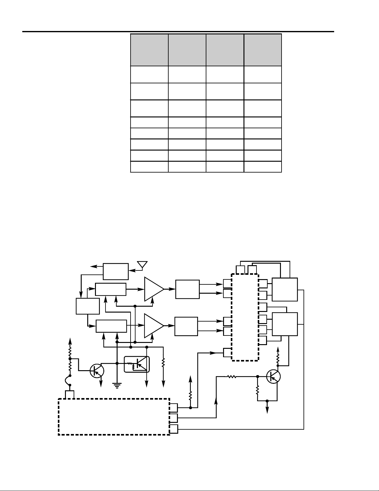
84 Tuner (Main) / IF
U17501 Pin
14
U17501 Pin
15
U17501 Pin
17
Cha nne l
Fre quenci e s
54-144
MHz
+11.7V +11.7V +0.3V
+0.1V +0.1V +4.8V
+11.7V +0.2V +11.7V
Cha nne l
Fre quenci e s
144-384
MHz
Cha nne l
Fre quenci e s
384-804
MHz
Q 1 7 5 0 4 B +11 .7 V +11 . 7 V +11 . 0 V
Q17504 C +0.4V +0.4V +11.7V
Q17505 C +0.1V +0.1V +11.7V
Q 1 7 5 0 3 B +11 .7 V +11 . 0 V +11 . 7 V
Q 1 7 5 0 3 C -11. 1V + 11 . 6 V - 11 . 1 V
Figure 7-10, Bandswitching Voltage Chart
There are two power supply voltages associated with band switching, the +12V and
+5V. If the +12V supply is inoperative, all bandswitching would cease. Since the PLL
depends on the +5V supply for power, if it were inoperative, bandswitching would cease.
However, if the +5V supply did not reach the PLL bandswitch circuits, the PLL would
still be operative, but the BSX line going to U17701, the Mixer/Oscillator would cease
switching. Providing all other circuitry is operative, the only symptom will be the tuners
inability to select band 3, and all associated channels.
RF To
PIP
UHF/VHF
Splitter
+12V
R17514
470
R17513
4700
14
BS1
BV/U
Q17504
U17501 PLL/DAC
Main/PIP
Splitter
UHF Single
Tuned
VHF Single
Tuned
+12V +12V
RF IN
Q17505
ANT
RF
Amp
RF
Amp
Loop Filter
UHF
VHF
-12V
BSX
BS1/2
R17516
6800
R17701
10K
15
17
5
Double
Tuned
Filter
Double
Tuned
Filter
+5V
4
5
U17701
6
7
11
R17510
10K
16
17
Mixer/
Osc
Q17503
R17511
100K
18
19
12
13
14
15
+12V
UHF Tank
Circuit
CR17701
VHF Tank
Circuit
CR17702
CR17703
-12V
R17512
100K
Figure 7-11, Band Switch Circuits
Page 85

Tuner (Main) / IF 85
Channel Switching
Troubleshooting the channel switching circuitry is straightforward and can be
accomplished by knowing the tuner voltages present during any channel selection. A
DVM (Digital VoltMeter) is all that is required to narrow list of possible component
failures.
RF To
PIP
UHF/VHF
Splitter
Main/PIP
Splitter
UHF Single
Tuned
VHF Single
Tuned
ST
U17501 PLL/DAC
RF IN
6
ANT
UHF
RF
Amp
VHF
RF
Amp
7
PRI
Loop Filter
Double
Tuned
Filter
Double
Tuned
Filter
SEC
17
16
4
5
U17701
18
19
UHF Tank
Circuit
CR17701
Mixer/
Osc
6
7
8
5
12
13
14
15
VHF Tank
Circuit
CR17702
CR17703
Figure 7-12, Channel Selection
PIN diodes and Varactors are used in the channel switching circuitry to shape the
frequency response of the tuner. If any of these diodes fail, the circuit that has the
failure will be unable to change frequency, resulting in locked or no tuning. Using a
DVM, the voltages coming from pins 6, 7 and 8 of U17501, the PLL IC, should be
checked first. If they are correct, follow the circuit path to the diodes. If the DC
voltage disappears at any time along the path, this will most likely be the cause of the
failure. In any event, the DC voltage path needs to be confirmed as operational before
any RF troubleshooting should be attempted. In most cases, component failure,
resulting in the loss of one or more DC voltages will be found. Capacitive diodes and
varactors for the CTC195/197 are normally replaced as a matched set. Consult the
service material for the chassis version for the latest information.
Page 86

86 Tuner (Main) / IF
No Tuning
The technician must further investigate a no tuning complaint before beginning
troubleshooting efforts to the component level. The following steps should assist in
those efforts.
1. Verify the on-screen display shows the channel change. If it does not, the problem lies
with system control, not the tuner.
2. There are four power supply voltages to the tuner. These are +12V, -12V, +33V and
+5V. These should all be confirmed to be OK.
3. Check the bandswitch voltages on pins 14, 15 and 17 of the PLL IC, U17501.
4. Check the output voltages of the bandswitching transistors.
5. Check the tuning voltages on pins 6, 7 and 8 of the PLL IC, U17501. Also note that if
a tuning voltage is "stuck" either high or low, there may be a problem in the PLL loop,
not the IC. Check the 4 MHz oscillator signal on the capacitor side of crystal Y17501.
Normal p-p voltage should be around 250 millivolts.
6. Monitor the LO voltage on pins 10 and 11 of the PLL IC. Normal operating voltage
will rise as channel selection goes up and lower when channel selection goes down.
7. Check the single tuned, and the primary and secondary double-tuned filter voltages at
the varactors.
8. Monitor the AGC voltage on the collector of Q32102, the ACG amplifier. Under no
signal conditions, it should be around +7.5 volts. If it is not, troubleshoot the AGC path.
9. Check the supply voltage to the RF amplifiers, Q17301 and Q17101. When they are
on, the supply should be 10 to 12 volts.
10. Check the IF supply voltages on the IF filter varactor diodes. The voltages should read
between 1.5 to 3.0 volts.
11. The oscillator tank circuit components may be checked using continuity readings with a
DVM.
Page 87

Tuner (Main) / IF 87
RF To
PIP
UHF/VHF
Splitter
Main/PIP
Splitter
UHF Single
Tuned
VHF Single
Tuned
6
ST
BV/U
U13101
System
Control
2
14
BS1
RF IN
U17501 PLL
3
C
D
4
1
ANT
RF
Amp
RF
Amp
UHF
VHF
7
PRI
18
19
Double
Tuned
PRI/SEC
Double
Tuned
PRI/SEC
SEC
C
BS1/2
D
Loop Fltr
5
8
L01
L02
BSX
10
11
15
17
4
5
6
7
1
2
11
16
17
U17701
VHF/
UHF
Mixer
Osc
10
9
IF Filters
VC1 VC2
18
19
12
13
14
15
Q17503
+12V
Filter & IF IN
U16201-9/10
UHF Tank
Circuit
CR17701
VHF Tank
Circuit
CR17702
CR17703
IF
Amp
To SAW
Figure 7-13 (Repeated), Tuner Block Diagram
Page 88

88 FPIP / 2nd Tuner
Main
Tuner
PIP
Tuner
Aux-1
Vid In
Aux-2
Vid In
WF01
Typical
System
Control
WF02
Typical
6
10
3
Vid-1
Vid-2
U26901
Video
8
Sw
C
WF04
Typical
34
Clk
2
C
4
Data
Bus
U13101
Figure 8-1, FPIP System Block Diagram
D
2
26
27
28
14
13
Ext.
S-Vid
In
B-OSD
G-OSD
R-OSD
WF00
Typical
51
1
5
28
27
26
FPIP
U18100
Vid-1
Vid-2
SV-C
SV-Y3
Clk
D-In
D-Out
WF08
Typical
To Kine Drv CBA
WF07
31
G
Data
43 44
32
B
38
40
30
R
Y
T-Chip
C
U16201
R-OSD
G-OSD
B-OSD
Clk
Typical
Y
41
39
C
34
35
36
WF06
Typical
WF05
WFXX
Typical
FPIP/2nd Tuner Overview
The FPIP circuitry is centered around the FPIP (Comb Filter/Pix-In-Pix) IC. This IC
is designed to be a 1-chip solution for the single moving picture-in-picture function. In
addition, it provides a digital comb filter for the main picture Y/C separation. The FPIP
contains analog switches to select from two composite or two component (S-Video)
sources from either the main picture or the small picture. The FPIP IC contains all A/
D’s, D/A’s, burst-locked clock, analog video switching, and RAM needed to perform
both the Pix-In-Pix and comb filter functions.
The FPIP IC can generate its own burst for timing references, if only a luma signal is
available. The PIP picture is cropped by 15% instead of compressed as in previous
PIP modules.
The design of the FPIP IC is intended to keep external components to a minimum. All
inputs are designed to accept industry standard 1 volt (p-p) video sources (a 20%
overhead is allowed), and all outputs are designed to provide industry standard 1 volt
outputs.
Page 89

FPIP / 2nd Tuner 89
In the following discussions, the larger on-screen picture will be referred to as the
"main" picture and the small window will be referred to as the "PIP" picture. The main
tuner will always be responsible for the main picture, while the PIP tuner will always be
responsible for the PIP window. If the two pictures are swapped, the main tuner will
retune to the PIP channel selection for the large screen presentation and the PIP tuner
will retune to the prior large screen channel selection and present it in the PIP window.
Page 90
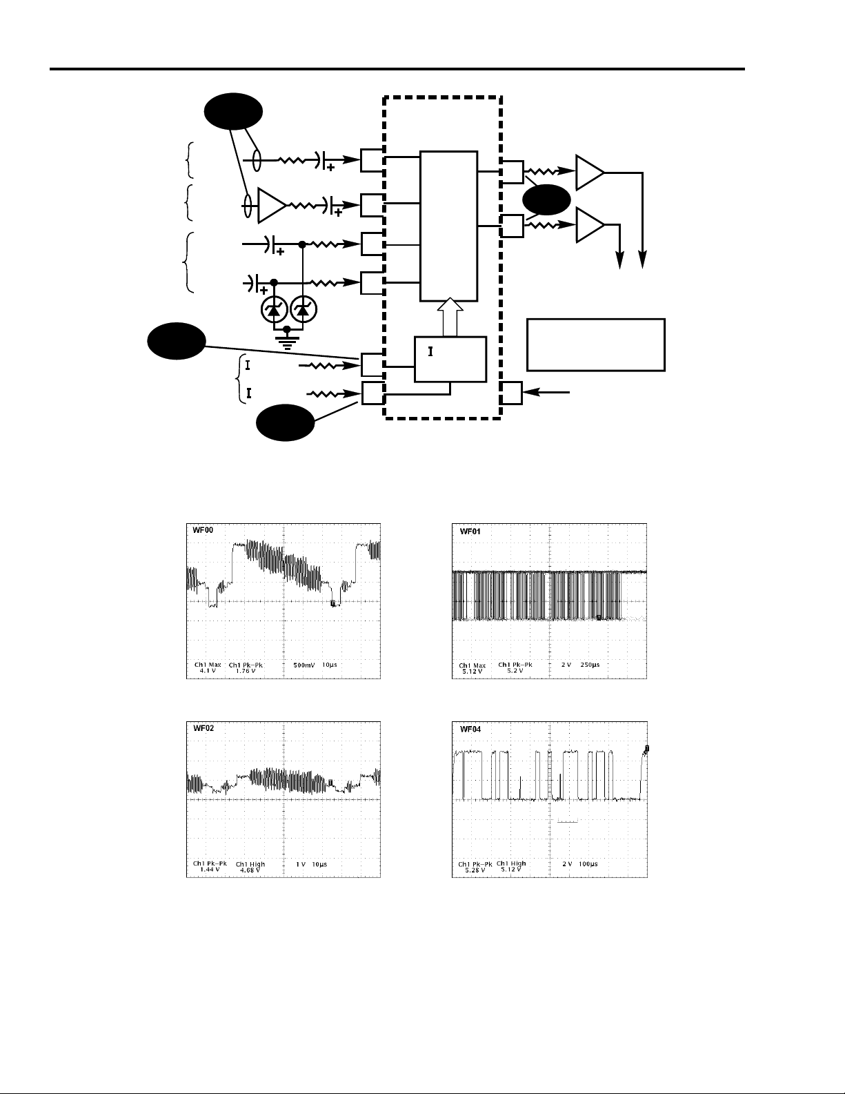
90 FPIP / 2nd Tuner
From
P26904-2
From
U16201-42
From
Aux Vid
Jacks
WF04
Typical
From Sys Ctl
U13101-4/3
WF02
Typical
PIP
Tuner
Vid In
Main
Tuner
Vid In
Aux 2
Vid In
Aux 1
Vid In
CR26902
+6.8V
Q12301
Buffer
2
C
Data
2
C
Clock
WF01
Typical
U26901
CR26901
+6.8V
10
6
8
3
2
4
Video
Switch
Switch
Matrix
2
Buss
C
Decoder
Vcc
Buffers Q26901
Q18109/Q18110
13
WF00
14
Q26902
Buffer
S-Video is input
Note:
directly to U18100,
FPIP Switching
9
Vid 2
To FPIP Switch
+12V Run
Figure 8-2, Video Input Switching
Vid 1
(51)
(1)
U18100
Page 91

FPIP / 2nd Tuner 91
Video Input Switching
Video input switching is accomplished via two integrated circuits. These are the
FPIP/Video Switching IC, U18100 and the Video Switch IC, U26901. The video
switch can have a maximum of eight inputs and six outputs. Only four inputs are used;
PIP Tuner Video at pin 10, Main Tuner Video at pin 6 and Aux 1 and Aux 2 at pins 3
and 8 respectively. Only two of the six outputs are currently used. Any of the four
inputs may be routed to either, or both of the outputs.
Zener diodes are attached to the aux inputs at pins 3 and 8 to prevent excessive video
input levels from damaging the IC. The internal switching matrix is controlled via the
I2C bus from the System Control Microprocessor, U13101, pins 3 and 4. The two
selected outputs exit the IC at pins 13 and 14. The composite video outputs are
buffered before they are applied to the FPIP Switching IC, U18100, at pins 1 and 51.
Although discussed later, it should be noted that the Video Switch IC has no provisions
for direct S-Video inputs. The S-Video signals are input directly to the FPIP IC,
U18100.
Page 92

92 FPIP / 2nd Tuner
WF00
Typical
Buffers
Q26902
Buffer
From Vid
Switch
U26901
Pin 13/14
From
S-Video
Jack
J26903
To/From
Sys Ctl
U13101
pin 3/4
Vid-1 In
Vid-2 In
WF19
Typical
S-Vid (Luma)
S-Vid (Chroma)
WF01
Typical
Clk
Data
WF04
Typical
Typical
+12V
Q18102
Buffer
Q26901
Q18109/110
WF18
Typical
Q18101
See Waveforms Page 94
51
1
3
5
28
27
26
WF10
Sync
V
Pulse
49
8Bit
D/A
Analog
Switch
(Main)
Analog
Switch
(PIP)
8Bit
A/D
2
C
Bus
Decoder
FB
Q18108
Luma
Y
Comb
Filter
8Bit
A/D
Y
Y
FSW
C
C
S-Vid
Switch
C
PIP
Process
10Bit
D/A
C
Y
U18100
FPIP Switch
Q18112/113
8Bit
D/A
43
Over-
Lay
Switch
C
8Bit
D/A
24
Buffers
WF09
Y
PIP
PIP
Y
C
47
45
30
C
39
Y
41
WF14
35
33
37
31
WF17
WF11
Q18107
FSW to
U16201-37
Q18104
Q18103
WF16
Chroma
WF13
WF12
PIP
Luma
WF15
PIP
Chroma
To Luma
Chroma
Process
U16201
Pin 38/40
Figure 8-3, FPIP Switching IC U18100
FPIP (U18100) Overview
The FPIP IC accomplishes most of the operation of the Pix-in-Pix function of the
CTC195/197. The FPIP contains analog switches, (to perform the swap and overlay
functions), A/D’s (Analog-to-Digital converters), D/A’s (Digital-to-Analog Converters),
a crystal clock, and digital circuits necessary to process and control the small overlay
picture.
The FPIP is divided into several sections; the PIP processor, clock, comb, analog and
I2C bus sections. The PIP Processor section includes the decode, encode and field
RAM subsections. The decode subsection takes a composite video waveform and
decodes it to Y, R-Y and B-Y for storage into the internal field memory. The encode
subsection which takes information stored in the internal field memory and encodes
chroma onto it, then outputs separate Y/C small picture signals which can be combined
to form a composite video signal for overlaying onto the main composite video signal.
The Burst Locked Clock section generates the clock signal for the system. The BLC is
locked to the color subcarrier of the main composite video signal. The analog section
converts between the analog and digital domain and performs video switching functions.
The bus section controls the FPIP functionality. Registers which hold control information
are distributed throughout the IC.
Page 93

FPIP / 2nd Tuner 93
FPIP Signal Switching
The FPIP IC serves as the center of the video switching circuits. The two selected
composite video signals from switching IC U26901 are input at pins 1 and 51(WF00)
after buffering. S-Video is input directly into U18100 at pins 3 (luma, WF19) and pin
5 (chroma, WF18). Once inside the IC, the S-Video luma and chroma signal are
combined to form a third composite signal. The three composite video input signals are
applied to two analog switch circuits within the IC. One is the “Main” picture analog
switch and the other is the “PIP” picture analog switch. The outputs of both analog
switches are applied to 8 bit A/D (analog-to-digital) converters. The uncombined SVideo input is applied to an S-Video switch.
The output of the analog switch processing the "main" signal is applied to an A/D
converter producing an 8 bit digital representation of the composite signal. From here,
the digital comb filter separates the luma and chroma information. After main picture
digital video is separated by the comb filter, the digital luma and chroma signals are
converted back to analog signals by an 8 bit (luma) and a 10 bit (chroma) D/A
converter. The luma signal then exits the IC at pin 49 (WF10), is buffered by Q18108,
and reenters the IC at pin 43 (WF09) where it is applied to the S-Video switch. The
selected main chroma signal exits the IC at pin 47 (WF11) for buffering and amplification
and reenters at pin 45 and is also applied to the S-Video switch.
The output of the PIP analog switch is also digitized and applied to a PIP processing
circuit that separates the luma and chroma signals and also a "Fast-Switch" signal
derived from the sync. The separate PIP luma and chroma signals are both converted
back to analog via two D/A converters. The analog PIP luma signal then exits the IC at
pin 33 (WF15), is buffered and reenters the IC at pin 35. The PIP luma is then applied
to the “Over-Lay” switch. The PIP chroma signal exits at pin 31 (WF16), is buffered
and reenters at pin 37. The PIP chroma signal is also applied to the overlay switch.
Remember the output of the Main Analog switch is processed by the digital comb filter
and always serves as the main picture except in the event that the S-Video signal is
selected as the main picture by the S-Video switch. The function of the S-Video switch
is to select between the output from the Main Analog switch and the S-Video input at
pins 3 and 5. The output of the S-Video switch always serves as the Main picture
video and is applied to the Overlay Switch. The PIP picture Y/C signals are also
applied to the Overlay switch. The Overlay switch combines the analog luma and
chroma (Y/C) signals of both the main pix and the PIP pix with the PIP signal overlaid
on top of the main picture. This signal is then output at pins 39 (luma, WF12) and 41
(chroma, WF14) where they are sent to the T4 Chip, U16201, pins 38 and 40 for
further processing.
Page 94
94 FPIP / 2nd Tuner
The FPIP Switch, U18100, is controlled via the I2C bus. However, the data line
from the microcomputer to IC U18100 is a two-way data communications line.
The data going to the IC (function and control information) is buffered by
Q18101 and input into pin 27 (WF04). The data coming out of the IC (status
information) exits the IC at pin 26 and is buffered by Q18102 before its sent
back to the System Control Microcomputer U13101. The I2C bus decoder in
U18100 is responsible for controlling all the switching circuits inside the IC
according to instructions from system control. For internal synchronization and
switching purposes, a vertical sync signal and a horizontal signal are combined
and input at pin 24 (WF17) of the IC.
Page 95

FPIP / 2nd Tuner 95
T
The PIP signal is sampled using a 4fc (Four times the clock frequency) clock locked to
the main picture burst. In order to avoid line to line jitter of the small picture overlaid
onto the main picture, the display of the small picture must be done using a 4fc clock
that is phase locked to the horizontal sync pulse of the display. While these two clock
signals have the same frequency, the phase of the two signals will be asynchronous with
respect to each other. The purpose of this circuit is to re-time the output samples.
Internally, FPIP does as much processing as possible using the input (or burst-locked)
clock. The PIP luma output D/A converter is clocked by the output (or line-locked)
clock. This circuit insures that data presented to the input of the PIP luma D/A will not
have distortion during the active video portion of the display. A Vertical Peaking circuit
takes the low pass filtered line difference signal (vertical detail) and processes it through
a nonlinear processing block and a gain stage. The gain is bus controllable (1, 0.75,
0.5, 0.25 and OFF). Vertical Peaking Gain is set to zero during vertical to preserve
Closed Captioned information.
From Vid
Switch
U26901
Pin 13/14
From
S-Video
Jack
J26903
o/From
Sys Ctl
U13101
pin 3/4
Vid-1 In
Vid-2 In
WF19
S-Vid (Luma)
S-Vid (Chroma)
WF01
Typical
Clk
Data
WF04
Typical
Typical
+12V
Q18102
Buffer
Q26901
Q18109/110
Buffers
Typical
WF18
Typical
Q18101
WF00
Typical
Q26902
Buffer
51
1
3
5
28
27
26
WF10
Sync
V
Pulse
49
8Bit
D/A
Analog
Switch
(Main)
Analog
Switch
(PIP)
8Bit
A/D
2
C
Bus
Decoder
FB
Q18108
Luma
C
Y
S-Vid
Switch
C
FSW
PIP
Process
10Bit
C
C
Y
Y
Comb
Filter
8Bit
A/D
Y
U18100
FPIP Switch
Q18112/113
D/A
8Bit
D/A
43
Over-
Lay
Switch
C
8Bit
D/A
Buffers
24
WF09
Y
PIP
PIP
Y
C
47
45
30
C
39
Y
41
WF14
35
33
37
31
WF17
WF11
Q18107
Q18103
WF16
Chroma
WF13
FSW to
U16201-37
To Luma
Chroma
Process
U16201
WF12
Q18104
PIP
Luma
WF15
PIP
Chroma
Pin 38/40
Figure 8-3, (Repeated) FPIP Switching IC U18100
Page 96

96 FPIP / 2nd Tuner
FPIP IC U18100 Pinout
The next pages contain a complete pin out diagram of
the FPIP IC and descriptions for the pin functions.
Pin Descriptions
1
CV_2
2
TEST6
3
SV1_Y
4
TEST0
5
SV1_C
6
VDD_AN
7
SV2_Y
8
VSS_AN
9
M_AD_BYP_T
10
M_AD_BYP_M
11
SV2_C
12
M_AD_BYP_B
13
M_AD_BYP
14
VDD_AD
15
VSS_AD
16
P_AD_BYP_T
17
P_AD_BYP_B
18
ANA_BIAS
19
ANA_FIL
20
VCXO_IN
21
VCXO_OUT
22
VDD_DIG
23
RESETn
24
MAIN_COMP_SYNC
25
GTE
26
IIC_DO
FPIP IC Pinouts
TEST1
CV_1
TEST2
COMB_YO
TEST3
COMB_CO
TEST4
SV_SW_CI
COMB_ADJ
SV_SW_YI
VSS_DA
Y_OUT
VDD-DA
C_OUT
PIP_Y_ADJ
OL_SW_CI
PIP_C_ADJ
OL_SW_YI
TEST5
PIP_YO
VDD_SRAM
PIP_CO
TEST7
VSS_DIG
IIC_C
IIC_DI
52
51
50
49
48
47
46
45
44
43
42
41
40
39
38
37
36
35
34
33
32
31
30
29
28
27
1 CV_2 One of the four Composite Video inputs
available as a source for either the Main Picture or
the PIP Picture
2 TEST 6 (Manufacturing Use Only)
3 SV1_YOne of the two S-Video Luminance inputs
available as a source of Luminance for either the
Main Picture or the PIP Picture
4 TEST 0 (Manufacturing Use Only)
5 SV1_C One of the two S-Video Chrominance
inputs available as a source of Chrominance for either
the Main Picture or the PIP Picture
6 VDD_AN Supply voltage, all analog blocks
(except A/Ds D/As and VCXO)
7 SV2_YOne of the two S-Video Luminance inputs
available as a source of Luminance for either the
Main Picture or the PIP Picture
8 VSS_AN Ground reference for pin 6, analog
9 M_AD_BYP_T Pin for bypass capacitor for
Main Picture A/D.
10 M_AD_BYP_M Pin for bypass capacitor for
Main Picture A/D.
11 SV2_C One of the two S-Video Chrominance
inputs available as a source of Chrominance for either
the Main Picture or the PIP Picture
12 M_AD_BYP_B Pin for bypass capacitor for
Main Picture A/D.
Page 97

FPIP / 2nd Tuner 97
13 M_AD_BYP Pin for bypass capacitor for Main
Picture A/D.
14 VDD_AD Supply voltage, analog (A/Ds and
VCXO)
15 VSS_AD Ground reference for pin 14, analog
16 P_AD_BYP_T Pin for bypass capacitor for
PIP A/D.
17 P_AD_BYP_B Pin for bypass capacitor for
PIP A/D.
18 ANA_BIAS Clock Generator Bias
19 ANA_FIL Clock Generator Bias Filter
20 VCXO_IN Timing Crystal Input
21 VCXO_OUT Timing Crystal Output
22 VDD_DIG Supply voltage, digital
23 RESETn Power-On Reset (active low)
24 MAIN_COMP_SYNC Composite Sync Input
35 OL_SW_YI Overlay switch Y input
36 PIP_C_ADJ Pin for bypass capacitor for PIP
Chrominance D/A Adjust D/A.
37 OL_SW_CI Overlay switch C input
38 PIP_Y_ADJ Pin for bypass capacitor for PIP
Luminance D/A Adjust D/A.
39 C_OUT Main Picture Chrominance with PIP
Picture Chrominance overlay output
40 VDD_DA Supply voltage, analog (D/As and
Sub-D/As)
41 Y_OUT Main Picture Luminance with PIP
Picture Luminance overlay output
42 VSS_DA Ground reference for pin 40, analog
43 SV_SW_YI S-Video switch Y input
44 COMB_ADJ Pin for bypass capacitor for
Comb D/A Adjust D/A. There is one adjustment D/
A for two Comb output D/A’s.
25 GTE Global Test Enable (Not used)
26 IIC_DO I2C bus data output
27 IIC_DI I2C bus data input
28 IIC_C I2C bus clock
29 VSS_DIG Ground reference, digital
30 TEST 7 (Manufacturing Use Only)
31 PIP_CO PIP Small Picture Chrominance
32 VDD_SRAMSupply voltage, digital
33 PIP_YO PIP Small Picture Luminance
34 TEST5 (Manufacturing Use Only)
45 SV_SW_CI S-Video switch C input
46 TEST 4 (Manufacturing Use Only)
47 COMB_CO Digital Line Comb Main Picture
Chrominance Output
48 TEST 3 (Manufacturing Use Only)
49 COMB_YO Digital Line Comb Main Picture
Luminance Output
50 TEST 2 (Manufacturing Use Only)
51 CV_1 One of the four Composite Video inputs
available as a source for either the Main Picture or
the PIP Picture
52 TEST 1 (Manufacturing Use Only)
Page 98
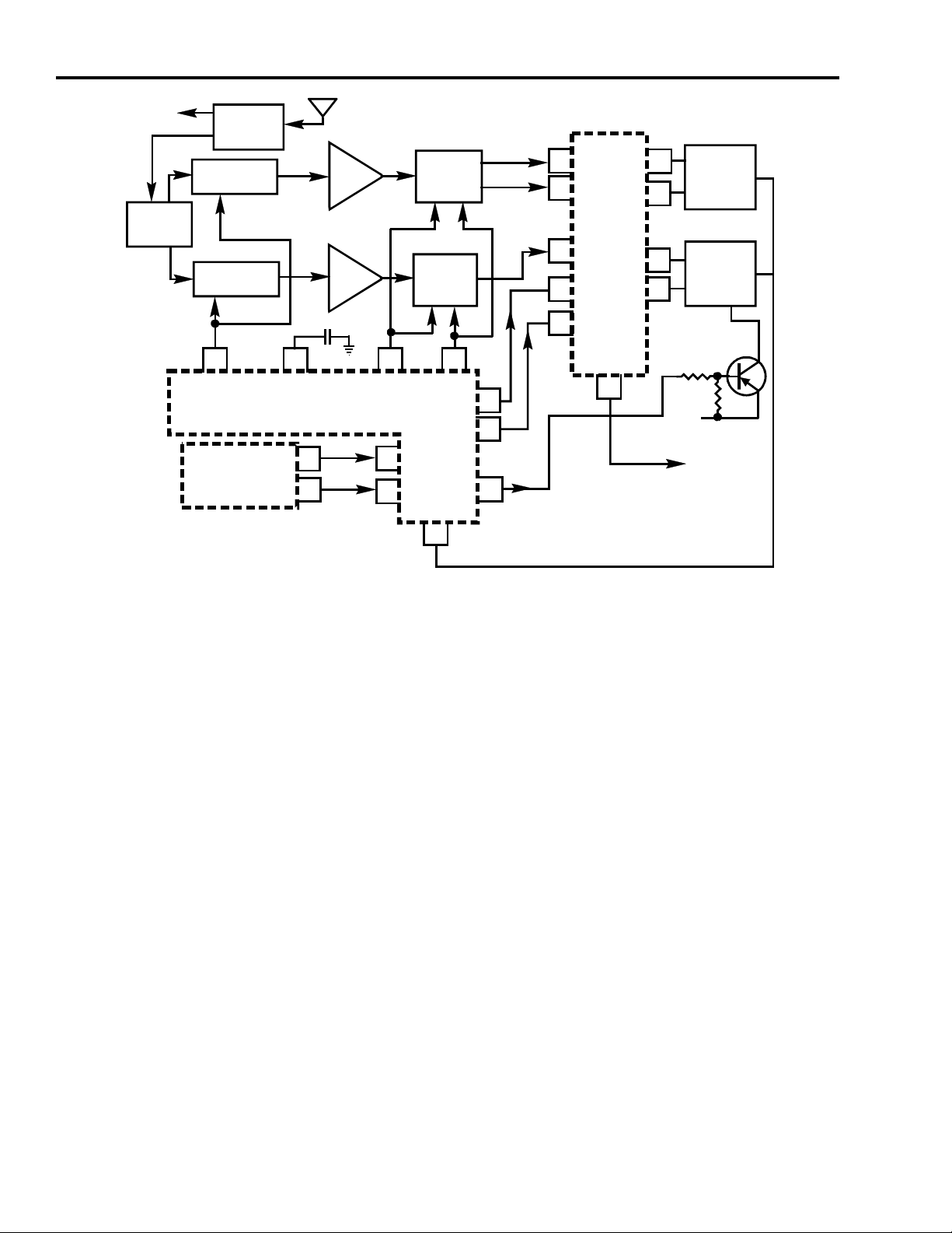
98 FPIP / 2nd Tuner
RF To
MAIN
UHF/VHF
Splitter
Main/PIP
Splitter
UHF Single
Tuned
VHF Single
Tuned
6
ST
U13101
System
Control
ANT
RF IN
10
L01
UHF
RF
Amp
RF
Amp
U17401 PLL
3
C
4
D
VHF
7
PRI SEC
18
19
Double
Tuned
PRI/SEC
Double
Tuned
PRI/SEC
C
D
Loop Fltr
5
8
BS1
BV/U
L02
BS1/2
14
11
17
12
10
4
7
2
U17301
VHF/
UHF
Mixer
Osc
IF
Out
1
14
16
9
11
UHF Tank
Circuit
CR17301
CR17304
VHF Tank
Circuit
CR17702
CR17703
Q17402
+12V
IF to
SAW
Filter
Figure 8-4 , Second Tuner
Second Tuner (PIP)
The second tuner, known as the PIP tuner, is very similar to the main tuner in the
CTC195 chassis. All functionality is identical to the main tuner. There is a separate
PIP EEPROM for the values required by the PIP tuner, IF and window alignments.
The tuner is capable of receiving off-air channels 2–69 and cable channels 01–125.
One difference is the front end of the tuner. Instead of dual control of the single-tuned
RF stage, the PIP tuner only has single control. Many of the input or output lines are
single-ended where the main tuner uses balanced lines. This means one side of the
signal is at ground potential. This makes signal transfers between the PIP module and
main chassis less prone to interference. The tank circuits on the VHF and UHF outputs
are also not as selective as the main tuner. In general, the picture quality needed in the
PIP window is not as great as that needed in the main window. That is why the main
window is always controlled by the main tuner. If the PIP and main windows are
swapped, the two tuners are retuned so that the PIP channel desired by the user, is
tuned by the main tuner and placed in the main window. The channel that was in the
main window is tuned by the PIP tuner and placed in the PIP window.
All alignments and troubleshooting efforts of the PIP Tuner are the same as for the main
tuner. The tuning bands are the same. The only differences are the alignment channels.
Figure 8-5 shows the table of alignment channels.
Page 99

FPIP / 2nd Tuner 99
Channel Band
2 1 57 55.25 101
6 1 85 83.25 129
98 1 111 109.25 155
15 1 129 127.25 173
17 1 141 139.25 185
18 2 147 145.25 191
9 2 189 187.25 233
29 2 255 253.25 299
39 2 315 313.25 359
46 2 357 355.25 401
50 2 381 379.25 425
M idrange
(M Hz)
Pix
Carrier
(M Hz)
Loca l
Os cilla to r
(M Hz)
51 3 387 385.25 431
61 3 447 445.25 491
75 3 531 529.25 575
101 3 657 655.25 701
114 3 735 733.25 779
122 3 783 781.25 827
125 3 801 799.25 845
Figure 8-5, Second Tuner Alignment Channels
Page 100

100 FPIP / 2nd Tuner
PIP 2nd Tuner/IF
Figure 8-6 is a block diagram of the PIP system with waveforms that may assist in
troubleshooting efforts. All waveforms were taken with a standard color bar input.
Ant
PIP IF
PIP
Tuner
(2nd)
EEPROM
U27903
Clk
6
From Sys Ctl
U13101-3/4 (Run)
1
Data
5
WF32
Typical
SAW
AGC
5
4
Q32101
WF01
Typical
WF04
Typical
3
4
Data
Clk
U27901 PIP IF
5
6
3
Amp
AGC
AGC
Delay
DAC0
Vid
IF
RF
20
9
U27902 D/A
Vid
Det
IF
AGC
VCO
19
11
DAC2
Converter
EQ
AFT
APC
DAC7
DAC6
WF31
Typical
13
10
16
15
Vid
Out
AFT
Out
2
U27904
3
4.5
MHz
Trap
WF29
Typical
Q27908
Buffer
Q27905
Sync
Sep
Q27906
1
2nd Tun
AFT
To System Control
U13101-10/18
Q27902
Sw
2nd Tun
Sync
Invert
PIP Vid To
Vid Switch
U26901-10
(J27901-1)
Buff/
Amps
Q27901
Q27903
Q27904
WF02
Typical
WF30
Typical
Figure 8-6 , 2nd Tuner/PIP IF Block Diagram
 Loading...