

Page 1
www.SteamPoweredRadio.Com
INSTRUCTIONS
BTE-108
E-1
Direct
FM
ES-27278
Quantity
1
2
See cable
*
of
crystals
and
Multiplex
-10B
ordered
. . .
..
ot
(N
OF
....
....
supplied
Exciter
FM
Unit
Crystal
Operating
of
Set
FCC
of
Set
Instruction
frequencies.
Unit
(Spare
Spare
Books
LIST
BTE
. . . . . . .
to be
Tubes
Tubes
Exciter
EQUIPMENT
...
co
. .
. .
be
27278)
. . . . . . . .
...
.
....
.........
..
ordered
..
Exciter (ES-
FM
Description
..
.
..
.
separately)
.........
-
..
.............
. . .
... ...
separatel
Reference
. . . .
....
...
.
.
....
.
. . .
....
y)
MI-34501
-34509*
MI
Ml-34510
IB- 30262-1
Description
ceramic, .01
feed
, ceramic, 5
or, ceramic, 2,200
ceramic,
1N34A
diode,
neon
amp
mount
shock
quantity
5-
*
Capacitor,
Capacitor,
Capacitor
Capacit
Capacitor,
Crystal
Lamp,
Fuse, 0.5
Mount,
minimum
thru
µf
- .00 l
µµf
µµf
10
shipped
µµf
.
RECOMMENDED SPARE PARTS
Symbol
Cl22,
Cll5,
4,
Cll
3,
Cll
6,
µf
Cl0
l32,
C
Ct69,
CI07,
l46
C
33,
Cl
l48
C
C214,
49, C
Cl
CRI0I,
DS!0l,
Fl0I,
Cl38, Cl40,
5,
l3
C
Cl80,
,
72
Cl
Cl27,
Cl20,
Ct50
47,
Ct
,
Cl56
Cl55,
Ct
Cl71,
Cl6
l60,
CR102, CR104
DS102
F102
,
77,
4
Cl4
4, C209, C211, C212
Ct8
Cl31,
Cl29,
Ct66
3, C207, C208,
Ct8
Cl26,
l24,
C
Cl52, Cl53, Cl57,
5,
Cl43,
C t34,
CI09,
30,
Cl
Cl44,
Cll0,
Quantity
5 73960
5 99177
5*
5*
2
5*
2 212327
Stock
77688
779
77865
59395
101857
57692
No
53
.
Page 2

www.SteamPoweredRadio.Com
E-2
0
)
••••••••
••••e ,,.. •
••••••••
••••••••
··~••11••
..
••-'••
~ 0
FIHAI.Mo'IP
c.,
T\IMllilt
0
92203
Figure
E-1.
BTE-108
FM
Multiplex Exciter
Page 3

www.SteamPoweredRadio.Com
TECHNICAL SUMMARY
E-3
ELECTRICAL CHARACTERISTICS
Type-of
F rt-quency Range
Power
Output
Frequency
Modulation
Carrier
Audio
Audio
Audio
Harmonil"
Fl\!
AM
Suh-carrier
Sub-carrier
Sub-carrier
Main-to-Sub-channel
Sub-to-Main-t·hannel
Power
Altitude
Ambient
Emission
Output
Impedance
Deviation
Capability
Frequenl"y
Input
Input
Frequency Response
Distortion
Noise
Level
Noise
Line
Slow
Voltage
Power
Crystal
Temperature
Stability
lmpedanl"e
Level
(referred
Level
(referred
Input
Level
Input
Impedance
Center
Frequency
Requirements
Variations
Consumption
Heaters
for
100'7,
mod
(100%
mod.)
00-15000
00-15000
(30%
Crosstalk
Crosstalk , .......
Range
to
to
..
l"ps)
I00
o/c, FM
carrier
mod
...
Range
......
. of
.
MECHANICAL SPECIFICATIONS
Overall
Weight
'Level
'Audio
curve.
"Distortion
measured
'
Subcarrier
if
required.
Dimensions
measured
frequenq
at
input
• response
includes
following a standard
modulation
(See
all
Subcarrier
. . .
(J
IO
I)
referred
harmonics
75
percentage
Modulation
using
to 75
up
µs
de-emphasis
can
400 cps
to
be
in
l"ps)
mod.) ....
voltage)
carrier)
. .... . .
. .
.. ..
tone
µs
pre-emphasis
30
kc/s
network.
brought
text.)
. . . . .
. . . . . . . . . .
.
and
is
to
50%
.....
....
. . . . .
'
Referen(e
by a 400
50- 15000 cps tones.
''Reference
by a 400 cps
kc/s)
by 30- 6000 cps tones.
on
main carrier.
F.,
88- 108
10
wall,
50
ohms
±
75
± 100
± 1000 cps max.
600/
+
10
±
I
db
0.
5%
-
Gs
- 50
5v
n1ax.~
10,000
.
,o
to
-
55 db'
- 65
240/208
±
5%
300
wa11s,
I
17
volts,
7500 ft .
-20
°C
Height
24½
"
80
lbs.
shall
be ± 7. 5 kc/s
cps
tone.
shall
be ± 75 kc
tone
. Sub-channel
mt-/,
k(/s
kc/s
150
ohms
± 2 db'm'
max.'
max."
db
max.
db
max.
ohms
67
kc/s
db
"
or
50-60
max
to
Main
min.
117 V,
Approx.
cps,
.
+45°C
Width
19"
deviation
channel
deviation
Subcarrier
single
phase
IO
walls
Depth
of
modulation
of
modulated
50/60
each
11"
the
suhcarrier
70%
the
main
JOO%
modulated
cps
by
carrier
( ± 7. 5
30%
Symbol
VlOl
V102
Vl03
Vl04
Vl0S
Vl06
V107
V108
Type
6AQ5
6AQ5
6AQ5
6CL6
5763
5763
6146
6AH6
Reactance
Reactance
Master
Oscillator
Subcarrier
Frequency
Frequency
Frequency
Power
Amplifier
Frequency
Function
Modulator
Modulator
Modulator
Tripler
Tripler
Doubler
Divider
and
(1/3)
TUBE
COMPLEMENT
Symbol
Vl09
VllO
Vlll
Vll2
Vll3
V114
V115
v116
Vll7
V118
Type
6AH6
6AH6
6AH6
6AU6
6AH6
12AT7
6AS6
2D21
OD3
lEPl
Frequency
Frequency
Frequency
Crystal
Crystal
Cathode
Off-Frequency
Off-Frequency
Voltage
Cathode
Divider
Divider
Divider
Oscillator
Frequency
Follower
Regulator
Ray
Function
Divider
Detector
Control
Tube
(1/4)
(1/4)
(1/5)
(1/5)
Page 4

www.SteamPoweredRadio.Com
E-4
DESCRIPTION
a frequency mod-
RCA BTE-10B, ES-27278,
The
ulated exciter which provides an r-f
any specified frequency in the 88 to 108
at
watts
compact
megacycle band.
subcarrier
a subcarrier
provide for
the main
to provide for various applications
such
authoriz!!d, stereophonic sound.
The
BTF-5B
replace the exciter units
mitters,
exciter
unit incorporates features which make it easy
adjust, easy to
All r-f multipliers,
ploy single-tuned circuits.
in a
generator.
the BTE-10B
power supplies and an oscilloscope
alignment.
The
conjunction with the BTX-1 A Subcarrier Gener-
fn
ator, will
rable
-noise ratio
co
of
programming
R-f
BTE-108 use relatively
cuits, thus simplifying
can be switched to read the
currents:
third
current;
The
citer simplifies
AFC
taneous checking
and
detector. Displays are in the
ures, with the advantages
can be observed easily. Checks can be
operation
way.
ther
o
modulator
FM
ckground
ba
as
BTE-10B
5KW
that
or
power
standard
BTE-10B
the main
to
the subcarrier will be somewhat limited when
multiplier
Modulator
multiplier
AFC
monitor
frequency dividers. A switch permits instan-
a check
without
type display requires no synchronization
This
adjustments.
The
stage which can be fed
generator
multiplexing
channel. Thus,
FM
of
output
maintain
cabinet rack
Employing
is
provide
and
the subcarrier separately.
control voltage;
of
such
one
music, and, if it
the exciter used in the RCA
is
Transmitter.
of
any ocher FM
of ten watts
nd
a
including
miniature
a self-contained unit
properl
when
subchannel
channel
FM
distortion.
power
and
broadband,
adjustment
cathode current; second
currents; PA cathode and
grid
oscilloscope
adjustment
adjus
and
the control action
disturbing
is
output
incorporates a
unit
the RCA
as
two subcarriers
or
designed especially
is
it
FM multiplex
of
should
can be used to
It
previous RCA FM trans-
smitters where an
tran
a
is
very reliable in operation.
output
the
exciter can be housed
The
together
and
tment
at
th
with
tubes
y adjusted,
perforn
regard
_with
frequency respon se
The
amplifier stages
single-tuned
built
. A
following
plate voltage.
and
incorporated
maintenance
ll
a
of
of
form
lock-in
the
of
AFC
of
I A to
BTX-
become
ate.
dequ
stage, em-
a subcarrier
throughout,
built-in
with
facilitate
co
and
compa-
ce
n
~a
signal-
co
of
n
-i
voltages a
in the
of
five dividers ,
the phase
of
Lissajous' fig-
divider
the
during
made
circuit in any
ten
from
on
The
co
used
the
or-
meter
nd
and
plate
ex
the
or
Power
The
-c
d
germanium
ments are
wave silicon rectifier.
All
a vertical chassis. Special hinge-type'
the bo
at
to be
components
supplies employ semiconductor rectifiers.
voltage regulated supply which furnishes
high
screen voltage utilizes a
and
plate
oscillator fila-
co
and
the
the
side.
employing
mounting
top
wiring
rectifier.
supplied
components
corners
ttom
swung
out
on
the
Modulator
by a d-c supply
the BTE-10B are
of
permit
access
for
underneath
CIRCUITS
the BTE-10B Exciter
A block
in Figure
which operates
two reactance
the main
the subcarrier; three frequency
output
the
the 88 to 108 me range; automatic frequency control
circuitry;
voltages
The
oscillator which operates
approximately five
desired
6AQ5
oscillator
pull, are inductively coupled to the place tank. R-f
voltages
out
90 degrees
Thus, one tube appears as a capacitive reactance and
other
the
oscillator tank.
ponent
audio voltage applied to the
the frequency
The
applied
by the
described in a later
The
6CL6, provides
the main r-f ca
s
on
to
deviation
Use
coupling
diagram
2.
channel;
stage to
and
for
master oscillator
output
reactance modulators
plate
the two
on
ase with respect to each other,
ph
of
out
appears
presented to the
mean frequency
to one grid.
automatic
third
part
ly a
of
the
of
circuit results in a highly linear operation
of
Circuits consist of: A master oscillator
carrier frequency;
the
I/18th
at
modulators
a
bring
power
these stages.
and
frequency.
and
,
of
as
The
the oscillator
of
frequency control circuit to be
paragraph.
reactance
for
rrier
the oscillator coil since the required
of
the r-f carrier
pushpull
of
provide
to
reactance
third
output
the
supplies to furnish a-c
a 6AQ5
is
at
me.
six
The
are
the grids, which
modulator
phase with the oscillator place.
an inductive reaccance across the
magnitude
tank
controlled
is
bias
This
modulator,
modulation
. This reactance tube
by
modulator
modulation
modulator
multipliers
frequency up to
a frequency between
depending
,
plates
connected to the
are
grids
the reactive com-
of
coil varies
tor
a
modul
varied accordingly.
is
by the bias voltage
voltage
an RCA
the subcarrier
of
the subcarrier
and
bridge
mounted
of
Hartley
of
are
180 degrees
and
the inductive
type
a full
pins
the chassis
circuit
and
shown
is
including
and
type
upon
the two
in push-
each
with
and
grids,
is supplied
Type
coupled
is
small.
is
on
for
for
d-c
the
is
the
on
Page 5

www.SteamPoweredRadio.Com
BTE-108 EXCITER CRYSTALS
E-5
Ml
No.*
Carrier
Frequency (
MC)
Crystal
Frequency
(KC)
Ml
No.*
34509-1 88.1 101.9676 34509-51
-2
·3
-4
-5
-6
-7
-8
·9
-10
-11
-12
-13
-14
-15
-16
·17
-18
-19
-20
-21
-22
-23
-24
-25
88.3 102.1991 -52
88
.5
88.7
88.9
102.4306
102.6620 -54
102.8935 -55
89.1 103.1250 -56
89
89
.5
89.7
89.9
90.1
.3
103.3565 -57
103.5880 -58
103.8194
104.0509
104.2824 -61
90.3 104.5139 -62 100.3
90.5
104.7454
90.7 104.9769 -64 100.7 116.5509
90.9
91.1
91.3
91.5
105.2083
105.4398 -66 101.1 117.0139
105.6713 -67
105.9028 -68
91.7 106.1343 -69
91.9
106.3657 -70
92.1 106.5972 -71
92
.3
92.5
106.8287
107.0602 -73 102.5
92.7 107.2917
92.9
107.5231 -75 102.9 119.0972
Carrier
Frequency (
98.1
98.3
-53 98.5
98.7
98.9
99
.1 114.6991
99.3
99.5
-59
-60
99.7
99.9
100.1
MC)
Crystal
Frequency
113.5417
113.7731
114.0046
114.2361
114.4676
114.9306
115.1620
115.3935
115.6250
115.8565
116.0880
-63 100.5 116.3194
-65
100.9
101.3
101.5
116.7824
117.2454
117.4769
101.7 117.7083
101.9 117.9383
102.1 118.1713
-72 102.3
118.4028
118.6343
-74 102.7
118.8657
(KC)
-26
-27
-28
-29
-30
-31
-32
-33
-34
-35
-36
-37
-38
-39
-40
-41
-42
-43
-44
-45
-46
-47
-48
-49
-50
93.1
93.3
93.5
93.7
93.9
94
.1 108.9120
94.3
94.5
94
.7
94.9
95.1
95.3
95.5
95.7 110.7639
95.9
107.7546 -76
107.9861 -77 103.3
108.2176
108.4491
108.6806
109.1435
-78
-79 103.7
-80
-81
-82
109.3750 -83
109.6065
109.
8380
-84
-85
110.0694 -86
110.3009
110.5324
-87 105.3
-88
-89 105.7 122.3380
110.9954 -90 105.9
96.1 . 111.2269 -91
96.3
96.5 111.6898
96.7
96.9
97.1
97.3
97.5
97.7 113.0787
97.9
111.4583
·92
·93
111.9213
112.1528
-94 106.7 123.4954
.95
112.3843 -96
112.6157 -97 107.3
112.
8472
-98
-99
113.3102
-100
103.1 119.3287
119.5602
103.5 119.7917
120.0231
103.9
120.2546
104.1 120.4861
104.3 120.7176
104.5 120.9491
104.7 121.1806
104.9
105.l
121.4120
121.6435
121.8750
105.5
122.1065
122.56~4
106.1 122.8009
106.3
106.5
106.9
123.0324
123.2639
123.7268
107.1 123.9583
124.1898
107.5
107.7
107.9
124.4213
124.6528
124.8843
• Suffixes 1
FCC
to
channel
100
designate
275, frequency 102.9 me.
channel
number.
Add
200
to
1uffix
to
get
FCC
channel
number,
e.g., Ml-34509-75
designates
Page 6

www.SteamPoweredRadio.Com
E-6
MODULATOR-OSCILLATOR
-,
7
CHANNEL
MAIN
AUDIO
INPUT
~---~
EMPHASIS
NETWORK
15,000
30 -
FROM
INPUT
SUBCARRIER
GENERATOR
30-67KC
'
I
I
I
I
6AU6
REFERENCE
I
CRYSTAL
I
I
lcARRIER
ON-OFF
I
LNTROL
PRE-
CPS
AFC
FREQ.
CONTROL
VOLTAGE
OSC
6AH6
DIVIDER
(1/5)
2D2I
OFFDETECTO
_ - -
FREQ
L
---
2-1N34A
DETECTOR
CATHODE
FOLLOWER
MIXER
6CL6
CARRIER
PHASE
l2AT7
6AS6
6AQ5
MOD
6AQ5
MOD
SUB-
MOD
6AH6
DIVIDER
3)
I/
(
6AH6
DIVIDER
/4)
(I
6AH6
DIVIDER
/4)
(i
6AH6
DIVIDER
5)
(I/
6AQ5
MASTER
osc
7
_J
I
I .-----.
5763
FREQ
TRIPLER
I
I
I
I
I
_L
I
I
I
I
I
I
I
I
5763
FREQ
TRIPLER
MULTIPLIER-PA
I
A
I
V
I
L
,--7
POWER SUPPLY
I
VDC
300
+
VDC
.3
+6
I
6 .3 VAC
I
L _
~~I
6146
DOUBLER1+----<
PA
._____,I
_J
I
I
I
_J
I
I
I
_J
I
RF
OUTPUT
88-108
I
I
I
I
MC
harmonic
low
very
with
reactance,
pure
a
almost
greatly
is
Moreover,
balances
Modulating
thus
main
the
reduced,
the
temperature
out
circuits
minimizing
channel°
pushpull
possibility
the
and
Figure
disto
loa
and
providing
modulator
s
and
y effectively
ver
are
subchannel,
rti
ding
better
upply
of
Block Diagram,
E-2.
on. Each
oscillator
the
of
AFC
utomatically
a
age changes.
volt
decoupled,
cross-talk
vice versa.
and
is
tube
action.
between
Exciter
FM
OB
BTE-1
Automatic Frequency
a
phase
an
control
automati
frequency
characterized
is
operation.
voltage
lock
derived
the
automatic
The
BTE-10B Exciter
dependable
of
develop
to
maintains
oscillator
actually
is
a
and
Control
control
A
between
signal.
.c phase
circuitry
long
by a
detector
phase
which establishes
a reference crystal
the
Thus
control
system which
the
of
record
used
is
and
system
Page 7

www.SteamPoweredRadio.Com
Cl98
E-7
INPUT
CONTROLLED
REFERENCE
FREQ
FREQ.
?JI
-
TO
REACTANCE
GRID
MOD
.
T
111
CONTROL
1N34A
1N34A
VOLTAGE
CI04
I
C 188
Cl89
Cl87
----
Rl68
~
+
Rl69
Rl70
+
-
Ll08
K IOI
1
CONTACTS
Figure E-3. Simplified Schematic,
achieves a stability precisely
crystal reference
the master oscillator signal
of
tions
the phase detector,
of
possible speed
circuit, the master oscillator frequency
must be reduced.
oscillator type dividers
Thus
240.
lowest audio frequency
± 100 kc deviation
within
precise frequency
an
the limits
limited pull-in
The
off-frequency circuit which extends the pull-in
± 400 kc
to
range
taneously provides a
possible off-frequency
and
Circuits
Figure
2.
sourcf.:.
the
of
This
maximum
the
of
linearity
of
control
(at
AFC
the
of
A small r-f
and
low
the
range
the final
safeguard
voltage
matching
confine
To
order
in
network
pass
accomplished in locked-
is
overall division
an
with
phase deviation
cps) is ± 58 degrees
(30
frequency),
final
the phase detector.
of
normally
is overcome by the use
frequency),
against
operation
system are
is fed
that
phase devia-
the
within
to
to exceed the
not
in
and
associated with
and
uncontrolled
.
diagrammed
the
from
of
the
swing
at
and
simul-
master
the
range
AFC
of
the
(at
well
of
in
Phase
OB
BTE-1
oscillator circuit to the divider chain where
divided by 240
that,
noted
be
modulation
± 20 cps.
to
through
ploying
same frequency, fed
the
obtained
reference crystal oscillator.
Operation
the simplified
diagram
lator
applied
10
Tl
90 degrees
but
signal
across the
by vector BA
across the
is reduced from a
cathode
a
two
by
Figure
of
exactly
is
its
to
Tl
and
applied
is
top
lower
Detector
a
to
the
at
the
From
follower
IN34A
dividing
the
of
diagram
4. Assuming
frequency,
on
the
,
grid
therefpre
11
of
out
Tl
to
half
Figure
in
half
It
kc.
25
20 to
of
range
same time, deviation
maximum
dividers, this voltage
a phase detector em-
to
diodes. A reference voltage
phase detector,
the
into
by five the frequency
phase detector
Figure
of
two
phase.
10,
the
of
represented by vector BC.
is
3,
that
no correction bias
with
signals applied
input
the same frequency
of
are
reference frequency
The
the voltage developed
and
secondary is represented
while
,
(a)
4
of
illustrated in
is
the
by
and
the master oscil-
the voltage
it
should
to
due
± 5 kc
fed
is
of
the
of
vector
is
is
to
Page 8

www.SteamPoweredRadio.Com
E-8
voltages are
two
These
phase.
of
degrees
signal
across its secondary
which
other
crystal rectifier
RI
E,
E,
Rl
Hence
R 169 to
should
signals
shown
is
Rl69
positil'e
R 169 will
correcting
lator
ships
negatii-e
tube
phase
stantaneously
High
filtered
C 188
out
to
pplied
a
is
90 degrees
is
voltage
The
two.
and
the
then
is
70)
E, respectively. Since
and
E, are equal,
and
70 will be equal
voltage
the
,
ground
If, however,
decrease,
and
in
greater
now
will be
correction
frequency
change
correcting
grid.
relationship
frequency
out
and
will
the
the
vector
their
Figure
the
C 189
4
than
greater
applied
be
frequency.
should
shown
as
any
Thus
corrected by a
components
the
of
and
magnitude
in
equal
controlled
The
the
and
11,
Tl
represented
is
phase
of
out
impressed across each
its associated
\'ector sum
d-c voltages across
the
and
as measured
zero.
be
frequency
relative
(b).
that
than
voltage
to
increase,
in
voltage
departure
between
control
choke
the
of
the
the
of
the
of
phase
relationships
the
Since
the
E,,
of
across R170
that
appearing
reactance
the
Accordingly,
the
Figure
applied
is
from
two signals
the
proper
the
of
voltage
L 108.
and
frequency
voltage
with
load
the series vol
from
of
magnitude
d-c
4
input
by
developed
vector
by
of
each
1N34A
(R169
magnitudes
69
RI
the
two
change
and
the
tube
the
if
and
reactance
the
90-degree
voltage
signals
capacitors
shown.
top
of
across
top
a
is
polarity
master oscillator
the
will
voltage
at
vector relation-
(c),
to
the
error
the
180
BD.
the
and
es
tag
of
and
of
input
as
E,
net
a
of
grid,
oscil-
net
in-
are
.
network
The
resistor R 168
and
98
CI
phase
the
difference
feeding
by
back to
then
both
in
The
the
to
grid;
out
C 187
tor
capacitor
master
automatically
in a
If
there
quency
changed.
detector
symmetrical
polarity
oscillator
To
developed,
the
of
T
at
0.1 kc will be
of
limit
the
causes
directions
amount
amplitude
in.
and
objectionable
is
(198
oscillator
paragraph.
later
signal
the
will be
of
However,
output,
change
to
toward
illustrate
take
master
which
111
capacitors
consisting
detector
that
small
a
reactance
master
the
at
frequency
of
of
to
der
_
or
audio
small
made
which
"hunting."
is
the
by
the
at
d-c
no
master
the
the
when
has a d-c
and
the
its
the
how
example
an
oscillator
0.1 kc low. A difference frequency
is
fed
of
control
extends
beyond
would
amount
tube
oscillator frequency to
the
signal
the
produce
frequency feedback, capaci-
and
switched
is
off-frequency
reactance
component
oscillator
beat
it
mean
correct
non-symmetrical
such as to
is
the
to
the
± 90
the
otherwise
beat
the
of
beat
This
grid.
difference frequency rate.
deviation
is
The
tube
frequency
not
is
component
frequency
frequency.
in
reactance
is
the
at
sufficient
paralleled
only
in
switching
detector
grid
and
will
locked in, is non-
which
produce
tube
(104, (187,
range
degree
reactance
is sinusoidal,
the
at
of
of
waveform
the
phase
imposed,
be
frequency
frequency
swing
proportional
with-
swing
larger
by a
when
done
is
described
mean
remain
phase
the
proper
the
master
the
frequency
a signal
grid,
of
tube
the
fre-
un-
is
and
A
----,1:EI
/ I
/ I
B
'
'
----~E2
C
/ I
/ I
'
,1
'
(a)
El
----~
- I
I
I
I
I
I
I
I
I
I
I
D
I
I
D
A
B
I
"
'
I
C C
-
'
-
,1
......
I
E2
~
A
B
........
_,,/
\
\
........
/
\
\
):
'
/I
\ I
El
I
I
I
I
D
',\I
......_~E2
Figure
E-4.
Phase
(b)
Detector
(c)
Signal Voltages
Page 9
www.SteamPoweredRadio.Com
E-9
master
the
the
The
the
of
junction
this
If
through
would
line
longer
no
The
Figure
frequency swings
and
its
approaches
increasingly slower,
produced.
of
is
frequency
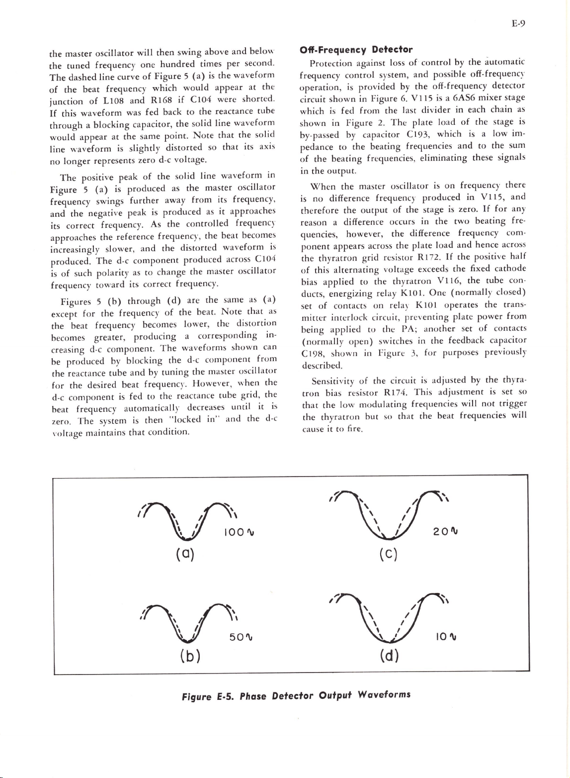
Figures 5
except
the
becomes
creasing d-c
be
the reactance
for
d-c
beat
zero.
voltage
oscillator
frequency
tuned
dashed
correct
produced
component
line curve
frequency
beat
L 108
of
waveform
blocking
a
appear
waveform
represents zero d-c voltage.
positive
(a)
5
negative peak
the
frequency. As
the
The
polarity
such
toward
the
for
beat frequency becomes lower, the
greater,
desired
the
frequency
system
The
maintains
will
hundred
one
Figure
of
which
68
RI
and
was fed back to
capacitor,
same
the
at
slightly
is
of
peak
produced
is
further
reference frequency,
and
componen
d-c
as to
correct
its
through
(b)
frequency
producing
component.
blocking
by
and
tube
frequency.
beat
fed to
is
automatically
then
is
that
the
point.
distorted
solid
the
as
away
produced
is
the
the
t
change
frequency.
d)
(
of
The
the
tuning
by
the
"locked
condition.
if
distorted
the
waveforms
reactance tube
swing
then
above
times
the
is
(a)
5
would
produced
a
appear
C 104 were
reactance cube
the
line
solid
chat
Note
so
waveform
line
master
the
its frequency,
from
it
as
lled frequency
contro
beat becomes
the
master
the
the
are
Note
beat.
corresponding
component
d-c
master
the
However,
decreases
in'"
below
and
second.
per
waveform
at
shorted.
waveform
solid
the
its axis
that
oscillator
approaches
waveform
CI
across
oscillator
same as (
chat as
distortion
shown
from
oscillator
when
grid,
until
the d-c
and
the
it
in
is
04
a)
in-
can
the
the
Off-Frequency Detector
Protection
frequency
operation,
circuit
which
shown
by-passed by capacitor
pedance
the
of
the
in
When
no difference frequency
is
therefore
reason a difference occurs in
quencies, however,
ponent
thyratron
the
this
of
applied
bias
ducts,
of
set
mitter
being
normally
(
C 198,
described.
Sensitivity
bias resistor
tron
the
is
that
thyratron
the
cause it to fire.
against loss
control
provided
is
in
shown
fed from
is
Figure
in
the
to
beating
output.
master oscillator
the
output
the
appears
grid
alternating
to
energizing
contacts on relay K
interlock
applied
open)
of
modulating
low
in Figure
shown
system,
by
6.
Figure
last
the
The
2.
CI
beating
frequencies,
across
the
circuit,
to the PA;
the circuit
but
frequencies
the
of
the
the
resistor R 172.
voltage
thyratron
KIOI.
relay
preventing
switches in
174.
R
that
so
automatic
the
control
of
and
the
15
VI
divider
plate
93, which
eliminating
produced
stage
difference frequency com-
plate
exceeds
10
another
for
3,
is
This
frequencies will
the
by
possible off-frequency
off-frequency
a 6AS6
is
in each chain
of
load
and
frequency there
on
is
zero.
is
two
the
and
load
the
If
the
16,
VI
(normally
One
operates
I
plate
set
feedback capacitor
the
purposes
adjusted
adjustment
beat frequencies will
detector
stage
mixer
the stage
a low im-
is
the
to
these signals
in V 115,
for
If
beating
hence across
positive
cathode
fixed
tube
the
closed)
trans-
the
from
power
contacts
of
previously
thyra-
the
by
set so
is
trigger
not
sum
and
half
con-
any
fre-
as
is
I \
I
:\
\ I
~
\ l
( 0)
'
V;
\
' I
\ l
(b)
Figure E-5.
'
100'\i
\
\
50'\,
Phase
(c)
(d)
Detector Output Waveforms
Page 10

www.SteamPoweredRadio.Com
E-10
V115
=
CONTROLLED
FREQ
.
REF
FREQ
Figure
Carefully
make certain
ing
shipment.
immediately
tion
company
may be recovered.
The
tainer,
separately.
only
external
and
connected
Reference
gram
of
wiring
A-C Power Line Connections
The
the
filament
operation
phase a-c lines.
unpack
that
reported
in
equipment
excepting
All
cables
should
this
book
to
be
used
primaries
transformer
from
no
Any
damages
order
is
tubes
internal
to
the
be
made
which
and
of
the
either
The
and
inspect
damage
or
to
RCA
that
lost
shipped
and
crystals
wiring
and
wiring
equipment
to
the
designates
the
proper
plate
transformer
(TI
14)
120-volt
equipment
has been
and
complete
is
C
193
V116
-
B+
E-6.
Simplified Schematic, Off-Frequency Detector
INSTALLATION
the
equipment
incurred
shortages
to
or
damaged
which
done
need
interconnection
connections.
are
or
is
shipped
should
the
transporta-
in
one
are
at
the factory,
be
prepared
at
installation.
the
cables
(TI
each
tapped
240-vo lt single-
with
to
dur-
be
material
con-
packed
diaand
13)
and
for
the
taps set
rnllllffled
care
are
Reference
diagram
for
110/
l'Olt
"Power
luad
The
in
by
near
should
TAL
for
must
made
and
making
to
disw1111ect
ten11i11al
The
a-c
Off-On"
switch
connections
the
overall
Tubes
should
reference
the
appropriate
be
I"
and
TO
FIL
TRANSF.
240-volt
011ly
to a 120-t·olt
be
taken
before
power
should
be
to
the
connections.
T
s
-I
(IIJl/
overload
switch,
( S 103)
of
schematic
be
to
the
inserted
"CRYSTAL
KIOI~
---s£l!
Tll2
use.
The
crystal heaters
a-c
source.
to
insure
that
proper
is
applied
made
table
Tramfor111er Primary
/ /
2-10
ll
2 ( black leads) f
2
of
T 113.
switch ( S 104) can be used
if
desired,
for
"Standby"
these circuit-breakers are
diagram.
inserted
type
number
sockets. Crystal
into
the
2."
co
the
/'()Ifs
in
their
designations
sockets
to
overall
and
connections
the
equipment.
is
wed,
ro111
the
plate
proper
Units
marked
Particular
schematic
d-c u,·er-
switching.
MI-34509
0:
UJ:,,:
I-
u
t: 0
::E
.J
(/)
0:
zW
<I'.
I-
0:
~
I-
11111st
Tap.1
b1:
S1tr1:
th
1:
120-
as
shown
sockets
printed
''CRYS-
b1:
a
Power
Taps
Line
to
be
Voltage:
Used:
TRANSFORMER PRIMARY TAPS
106 117
2-4
3-4
---------------
Tap C of
"AC
OVERLOAD"
Circuit
128
1-4
Breaker
208
197
3- 5 2- 5
I
I
"AC
Circuit
219 229
1
-5
3--6
Tap B of
OVERLOAD"
Breaker
240
2-6
251
1-6
Page 11

www.SteamPoweredRadio.Com
E-11
crystals
and
tubes
After
to
properly
equipment.
the
crystals heaters to reach
the
before
following
DSl0l
patterns
the
on
of
these displays may occur in indi-
from
nections are
applied
and
tubes
temperature
below.
the
Tune-Up Procedure
were
of
Indicators
crystal oven heaters
oscilloscope
The
obtained
an exciter unit.
sidered as typical
·iations
de,
are
made, a-c
Allow
the
DS102
and
on.
are
illustrated
built-in
These
patterns
those to be expected;
vidual units.
I.
"DS
\X
101
1
ith
··
the
and
equipment
102"
"DS
operating
extinguished,
the crystal heaters have reached
· switch to
(Sl06)
control
face
the
on
183)
(R
(S102)
to
(Reading
"OFF-FREQUENCY
76)
( R 1
the
the
adjust
CRO
"
"AFC-OFF"
Switch
INTENSITY"
appears
"FOCUS"
, switch
ture
With
,·ance
until a trace
Then
Switch meter-switch
voltage.
plate
check
and
Turn
66.)
and
54
LOCK
SENSITIVITY"
wise position.
switch to
CRO
Turn
2.
of
screw
of
Adjust
3.
Pattern
Set
4.
top
pattern.
CRT
.
top
should
loops.)
vertical size
master
the
frequency
screw
indicating
have
Adjust
size
factory)
Lissajous' figure
(
right-hand
maximum
operating
frequency. E.g., 88.1
master
brated
TI03
of
( fine)
Turn
5.
adjust
division
NOTE
ing
and
more.
division
Turn
6.
adjust
division
oscillator
receiver
to
adjustment
CRO-Switch to
T14
ratio
:
screw
possible
a
Too
racio.
CRO-Switch to
T105
ratio
frequency.
frequency meter. Use
or
make
to a mid-position.
stationary
a
for
/3.
1
of
high
Too
is all che
division
an
low
stationary
a
for
/4
1
of
Adjust
which
this
an
indunance
"XT
for
LI I 2
/8"
( I
Tl
of
a division
left-hand
five
top
pattern.
of
oscillator
is
corresponds
me
adjustment
"lST
Figure
See
inductance,
in,
way
racio
"2ND
(Figure
to 3 / I
15
1 /
Use
Lissajous' figure
means
Lissajous' figure
7
in place,
and
power
sufficient time
tune-up
light
will
m these pages
during
CRO
should
and
indicating
operating
"OFF"
position,
any
in
185) clockwise
(R
tube
the
of
proper
for
,.
should
extreme
to
DIV"
E
be between
"Vl07
AL
maximum
will be satis-
6"
obtain
to
ratio
loops
of
screw
Figure
See
approximate
the
to
final
the
of
18
to 4894 kc
grid-dipper,
bottom
setting
position
DIV"
7 b.
che adjusc-
when
frequency
low
a
or
4
I/
of
may resulc in a
position
DIV"
c).
all concan be
for
operating
procedure
when
tune-up
be con-
slight
indicators
that
temperaposition
ad-
18).
(VI
sharpness
" posirion
INTER
clock-
position .
horizontal
stationary
/5.
I
of
five
and
for
Tl09
a.
7
carrier
cali-
screw
top
the
and
and
or
/5
I
1/2
and
anq
CRO-Switch to
Turn
7.
stationary
a
for
division
Turn
8.
adjust
division
zontal
Turn
9.
square
A
senting
change
T!06
(Figure
1/4
of
ratio
CRO-Switch
TI
ratio
size
07 for
of
stationary
1/5
of
pattern
.
CRO-Switch to
medium
of
an unstacionary Lissajous' circle.
circle
the
of
adjust
ence between the reference sighal
signal.
both
signals
both
changing
make
03
TI
(T104
stationary
a
on
switch
adjust
peak
adjustment
Lissajous' circle.
"ON
to
1)
completely
a
addition
In
age
lt
vo
with
With
.
.
-
master
Tl03
point
oscillator
slowly in
where
in a slowly
variation
that
If
again
of
all dividers
nearly
a
starting
quency.
a slowly
If
10.
s,,itch
position
ING"
Tl03
slowly
switch (S
"jump"
Figure
tector
built-in
-
should
meter
and
( C 105) for
bottom
moving
IO
into
f.)
7
output
meter,
AFC"
give nearly zero readings.
position.
frequency differences
few cps can be observed
sensitive
more
A
11.
TUNING"
50 cps
at
connector
indication
modulation
a
of
L104 to
with
12
and
11
frequency. So,
switch in
CRO
the
be
fine
should
"AFC-OFF"
a
a
LATOR
applying
input
audio
maximum
for
centage
Tune
12.
meter
06"
VI
Steps
13.
oscillator
and
off
circle
the
with
03
TI
Then
throw
GRID
meter
(MlOI)
position.
with
position.
position
DIV"
"3RD
Lissajous' figure
.
d)
7
position
DIV"
"4TH
to
Lissajous' figure
Adjust
(
brightness
depends
somewhat
changing
TI08
.
e)
7
figure
"PHASE
should
the
on
Rotate
directions
agree
the
trying
in frequency
Lissajous' circle.
as you
sure
TI07)
-
circle
are still locked in.
cannot
higher
circle was
'VIOi
(SI02)
"l\lODULA
to '
indication
TOR
.
may be
Then
" position.
stationary
CRO
the
to
" position.
DET
be seen repre-
rate
The
frequency-differ-
divided
the
and
bottom
screw
to find
resulting
During
obtained,
be
or
frequency
lower fre-
change
obtained.
Vl02
&
GRID
resetting
Slight
switch
circle
to
"AFC"
required
The
circle now. (See
phase de -
the
maximum
for
can be observed also on the
on,
phase
the
(CI05)
and
),
the
switch in "
positions
both
AFC
With
detector
up
meter.
"MODU-
of
can be
t- 10
made
db
adjusting
modulation
meter
the
AFC
the
at
with
adjustment
approximately
101
(J
on
monitor.
maximum
meter
may
made
control
slightly
AFC
near-stationary by
indication
switch
(S102)
change
ld be switched
shou
on
DET"
top
"PHASE
knob
switch back
the
position
the
of
to
and
and
and
and
hori-
of
of
the
the
try
i-"
I
TUN
of
obtain
should
or
off,
to a
by
to the
C105
per-
the
of
"I
tn
master
tuning
can.
"AFC"
a
a
-
,
Page 12

www.SteamPoweredRadio.Com
E-12
. ( a J
"XT
Switch
AL
DIV."
Position:
f1 /SJ
( b J
"1st
Switch
DIV."
Position:
f1
/3
J
f c J
"2nd
Switch
DIV."
Position:
f1/4J
( d J
Switch
"3rd
NOTE:
frequency range. It is
adjusted
of
switch
turn
the
Start
number
end
of
TI07,
14.
meter
NOTE:
100 me.
15.
meter,
Tl04
so
their
lock-in
CRO-Switch
tuning
divider
turning
of
of
the
revolutions
and
TIIS
Tune
L105 to
switch
in
Remove
Tune
Cl37
meter
Position:
DIV."
revolutions
range.
to
that
they
screw
unlocks
screw
counted.
.
"l
e
V107"
C214
f1/4J
TI07
stay locked in
desirable
normally
range
. In
to
"1ST
on
top
(Lissajous'
to
the
until
Turn
screw
Repeat
maximum
position.
for
"PLATE
Figure
to
operate
order
DIV"
of
TI04
figure
right
it
unlocks
back
this for
indication
center
TUNING"
switch in "Ik V107"
E-7.
over a certain
have
TI04-TI07
in
the
to
assure
position.
to
the
left
gets "fuzzy")
and
observe
at
the
half
the
TI05,
frequencies
or
better
( e J
BTE-108
middle
this,
Now
until
the
other
number
Tl06,
of
meter;
above
to
dip
Switch
"4th
.
on
in "II'
Position:
DIV."
f1 /SJ
Oscilloscope
Vl07"
to
obtain
or
desired
mum
used in the
DC
of
plug
in
"POWER
16.
detector
graphs.
Then
(fJ
position.
proper
output,
output
Patterns
Adjust
grid
then
.
(If
a Micromatch
output
Switch
"PHASE
Cl39
"OUTPUT
current
in
retune C 13 7 for
transmission line, the developed
Position:
DET."
TUNING"
following
dip
or
Reflectometer
voltage may be fed into the exciter via
Tl05
and
indicated
OUTPUT"
Adjust
NOTE
to
assure
the
(V
116)
as
CAREFULLY:
sufficient pull-in
sensitvity
proceed with Steps 17, 18, 19
on
the meter,
position.)
described in
This
adjustment
range
of
of
the
,he
following
the
and
is
exciter.
meter
off-frequencr
important
20.
amplifier
or
maxi-
is
pin
8.
switch
para-
Page 13

www.SteamPoweredRadio.Com
E-13
"OFF-FREQUENCY INTERLOCK" Adjustment
16)
off-frequency
the
Sensitivity
controlled
INTERLOCK
the
in
can be
ment
50 cps
slightly
Using
input
An
quired.
energized, as observed by
is
the
of
cutout.
will be
a
If
method
Modulate
turn
and
is
K 10 I
clockwise
setting.
and
gized
of
setting
the
by
SENSITIVITY"
cathode
circuit
obtained
source,
tone
follows:
as
a 35-cycle tone,
signal
Turn
relay
The
correct
the
cps source
35
of
R 174 counter-clockwise
operation
bf
or
at
point
setting
using a 50-cycle
exciter
the
R 174 counter-clockwise to
energized.
until
Then
Note
101
K
set R 174
de-energized positions, which will be the
detector
"OFF-
the
of
potentiometer
this stage.
of
either
by use
although
of
the
modulate
approximately
listening
PA
the
of
which relay K
R 174.
for
available, an
not
is
source may be used.
tone
with
3G%
l
this setting.
de-energized,
is
halfway
between these ener-
the
the
(VI
FREQUENCY
(RI
Proper
adjust-
cps
35
a
methods
exciter I
db
n
relay KIO 1
until
closing
the
for
screen
or
plate
energized
1s
I
10
alternate
50-cycle tone,
where
point
the
turn
Then
noting
differ
30%.
is
R 174
1s
74)
or
re-
this
Set
17.
sition
burn-in
18.
the
Fina.II)',
adjustment.
action by
"OFF"
to
the
on
Retune
CRO-Switch
and
of
crystal
capacitors (
center
correct
control
(Sl0l}
control
relay K 101.
po
vent
tune
trimmer
signed
final frequency
NOTE:
adjustment
,han
.
19
possible to
20.
obtained
tuned
or
stage
Frequency
2 kc.
±
Reduce
prevent
Multiplex
with
maximum
for
maximum
for
Check
switching
slightly
and
Tl03.
of
top
03 to
TI
(S106} to
reduce
"INTENSITY"
pattern
the
the
using
"FREQUENCY
(205)
frequency.
approximately
rnn
also.
12
LI
of
"INTENSITY"
CRT
Operation.
multiplier
all
grid
power.
-frequen
"AFC
should
setting.
off
SWITCH"
the
proper
for
the
detuning
This
original
"PHASE
(Rl85)
.
station
frequency
ADJUSTMENT"
and
((205
be
Do
(206)
(
or
15
±
changed
noc
(Rl85)
to
(206
kc.)
slightly
change
as much as
will
"burn-in".
Best crosstalk will be
amplifier
and
following
the
current
in
cy
vernier
energize
DET"
to pre-
monitor
as-
the
vary
by
more
stages
operation
daily
In
heaters should be
power
application
short
observing
by
the exciter
The
the
in
sent
exciter
the
These
regular
exciter.
the
The
and
emphasis at
unit
in place
ator
Numbers
socket
the
resistors
of
warm-up
period,
the
the
on
is
oscillograms
INSTALLATION
desired
the
proper
for
oscilloscope
operation
pre-emphasis
,s
75
1
can be
removed
some
removed, an 18
is
pre-emphasis
the
of
can be
made
the
on
I.
IO
XZ
recommended
is
the
of
on
left
the
to
performance
patterns
air.
shown
section
adjustment
operation
patterns
without
it
if
point
other
db
in accordance
up
diagram
use
The
.
equipment,
continuously.
exciter,
and
can be checked
oscilloscope
the
on
tuning
the
with
this book repre-
of
various stages
the
of
the
of
may be observed
affecting
network
is
pad
network.
performance
a
is
desired to
system.
the
in
should
Such an attenu-
with
identify
of
the
5";~ tolerance,
±
the crystal
Then
allowing
procedure
system.
AFC
during
plug-in
apply
inserted
be
Figure
pins
octal
½
OPERATION
through
after
while
unit
pre
this
If
watt
a
of
of
8.
of
in
used
corporating
sh
half
stage
ing
the
remove
-
range
the
with
be
ould
is
it
If
the
of
should
procedure
Remove
I.
cover
the
3
5
If
doubler,
exciter
the
an
the
FM
amplifier,
44 to 54 mes.
of
previously
a frequency
in
made
necessary
providing
designed
exciter.
the
that
final frequency, modification
accordance
in
made
be
conversion coil.
the
using
exciter unit. Remove
the
from
power
all
enclosing
tube
6146
470
components
(V107}
of
.
470
150
exciter
frequency
to be
is
output
transmitters
this modification
one-
operate
with
the
on
output
the
of
foliow-
the
final stage,
in -
and
4
6
Output Frequency Conversion
A conversion coil
modify
exciter
the
to
(Ml-34501-2)
stage
last
the
supplied
1s
to
a
straig
with
ht
-
Figure E-8. Schematic,
18
Attenuator
db
Page 14

www.SteamPoweredRadio.Com
E-14
(L107)
choke
r-f
Unsolder
2.
through
plate
the
bracket
holding
install
sure all
and
½-inc
the
cover
ment
modification made,
10
Main
be set
generator
indicates
can
the
Put
3.
C 146
h clearance
cover
4. Reinsert tube V 107 in its socket,
in
and
15
and
NOTE
may be
ced
redu
more
required.
is
Carrier Deviation
Approximate
without
the
capacitor
component
then
plate
the
coil
new
mounting
mounting
such a way
in
in position.
is
This
place.
power
plate
watts.
an
In
:
replaced
power
availab
readily
deviation
a
the
and
amount
the
(Cl46),
be
coil
screws
between
emergency,
ou
and
mounting
(L106).
are
that
L107
now
can
should
No
.
le
to
back in place,
output
the
change
turned
(Ml-34501,
bracket
completes
power
by an RCA 2E26,
tput,
by
of
shown
subcarrier
of
using
monitor,
chart
remove
Remove
tight.
the
the
in
the
from
that
units
place.
bracket
gain
Item
there
and
be
RCA 6146
the
the
in
access to screws
this coil,
its place.
in
2)
Re-solder L107
will be
cover
the
install the
and
modification. Fila-
at
(YI07)
somew
tube
r
With
ections
applied.
will be
latte
in conn
Subcarrier
carrier
main
subcarrier
a
only
The
Figure
9.
voltage
necessary
feed-
hold
The
and
making
least
at
when
the
between
hat
be
can
chart
input
the
at
produce
to
indicated
As
frequencies
lower
of
selected.
same
tolerances
mended
with
so
multiplex
produce
nator
subcarrier.
should
mum
with
channel.
as well as
Therefore,
current
crosstalk.
frequencies.
the
main
above
The
or
2
by
is
with
remain
Proper
grid
minimum
main
that
a
into
BTE-lOB Exciter (J-102
the
of
required
the
on
require
carrier
a 32.5 kc, 2.6 volts will
At
channel
method
the
in
the
other
3
measuring
receiver
voltage
15
±
Using
the
setting
current
Detuning
subcarrier
L-104
following
the
deviation.
chart,
the
slightly
To
at
deviation.
order
reactance
6CL6 tubes.
relative
(with
0.1 to 0.2 volts
of
deviation
kc
several 6CL6 tubes this
same.
L-104
of
into
subcarrier
of
deviation
should
more
obtain
67 kc, 3.6 volts
approximate
is
25
±
of
tube
main
in
2nd
the
-cteviation
L-104 will increase crosstalk
be
tripler
higher
the
voitage
10 kc
±
a
percent.
V-104 be
method
One
subcarrier
program
the
of
BTE-
the
tripler)
the
of
to
set
stage
or
subcarrier
than
deviation
should
produce
subject to
and
is recom-
It
compared
of
voltage. A
should
off)
discrimi-
the
at
by
main
voltage
( maxi-
JOB
will coincide
the
of
carrier.
main
maximum
minimum
for
J-106)
the
be
the
doing
the
main
grid
chart
This
frequency
'°
0
.,
ii
0
8
n,
t----t----t-----11-----+---+----,.---t----+--------11------t
0
.,
I-
C
6
laJ
<
"
I-
..,
0
>
IIC
I&,(
2
a::
a::
~
ID
:)
.,,
0
indicates
deviation.
4
DEVIATION
amount
the
subcarrier
of
a
(MAIN
12
voltage
.,
CARRIER
necessar
20
SUBCARRIER)
BY
the
at
y
67KC
input
of
24
the
28
BTE-10B
32.5KC
8520017
Exciter
ICC
to
produce
a specific
Figure E-9. Main
Carrier
Deviation
by
Subcarrier
the
(Chartl
Page 15

www.SteamPoweredRadio.Com
Fig
UG
57
8/U
ADAPTOR
JIO3
ure
E-10. Connections for
M.
C.
TYPE
39OOil
JONES
573N4
Measuring
TO
PIN 8 P1O5
TO
PIN
Power
E-15
7 PIO5
Output
Subcarrier
To
47K
ohm, ½ watt
parallel
Use
of
The
With
required
replacement
Modulation
increase
to
Rl95
Control
exciter can be
normal
except a periodic check
of
same type.
Failure
failure
denced by
frequency
(Terminals
the PA
of
of
a tube
operation
detector
No. 5 and
stage
automatic
of
a defective tube,
will be
without
ment
sary to
for
Emergency
trol
automatic
be
or
restored
need
of
circuit
realign
tuning
Provision
should
warned
by
the
erratic
for
presented
Operation
is
made
tupes
frequency
of
the
monitor.
Tube
or
component
cases by
each
found
switch
in
the
of
{S106)
AFC
switching
its positions
identifying
may
circuits.
subcarrier
modulation
resistor
or
Rl97.
Tones
modulated
care, no
defective ones
frequency
or
other
of
the
circuit,
No. 6 of
the
transmitter.
proper
by
replacement
operation
readjustment.
components
the
exciter
is
following
under
for
maintaining
or
components
control
loss
of
control
performance
failure
the
meter
until
the
difficulty.
also be
helpful
percentage
should
be connected in
by
control
maintenance
of
all tubes
with
new tubes
control
component
relay K 10 I in
opening
)105)
If
failure
of
of
the
defective
However,
made,
it
will be neces-
the
INST
ALLA
frequency con-
associated
fail.
The
operator
by loss
of
the
carrier
can be
found
switch ( S 102)
an
abnormal
The
in
locating
, a
tones if
MAINTENANCE
should
due to
will be ev
the
that
the
if replace-
procedure
TI ON.
of
frequency
reading
oscilloscope
of
the
contacts
control
is
due
exciter
tube
with
will
carrier,
in some
through
trouble
be
and
the
the
i-
off-
to
the
is
desired.
the
into
exciter.
this
be
carrier
These
rang
e between 20 kc
one
of
the
With
point
, 30%
obt
ained.
If
the
master oscillator
frequency can be
control
tones,
and
subca
rrier
input
approximately
modulation
is
controlled
which
35
kc,
jacks
5 volts
of
the
main
functioning, the
lows, until such time as repairs can be
I. Remove the
trol tube
2.
in first
output
by
3.
the
Turn
Slowly
(V116).
one
frequ
frequency
Stability
such
that
quency to
periods
of
adjustment
CAUTION:
d-c
power
fore, care
more
the
fila111e11t.
remaining
the
direction
of
after
± I kc (
time
of
tha11
202
I "
OFF-FREQUENCY'
"AFC.OFF"
rotate
the
switch
top adjustment
and
then
the
(SI0I)
other
ency to its assigned value as indicated
monitor.
the
master
sufficient
at
. Possible
Tl03
top
The
supply
should
two
Otherwise,
warm-up
the
screw.
voltage of
will
1·ary
be
of
the
oscillator
it
final
frequency)
drift
can be corrected by
the
with
load. There-
take11
11ot
tubes
having
damage to
d-c bn1ted tubes or to C202 may
result.
Power
veniently by use
coupler
the
position,
nected to Pin
tive
Power
meter
terminal
Output
output
such as
switch
the
positive
No. 7 (ground)
to
Pin No. 8
Measurements
indications can be
of
the
meter
( M 101)
the
M.
C.
Jones
(SI02)
in
the
terminal
"POWER
of
of
of
P105 .
Micromatch.
the
PI05
Readings
are
generally
should
()106)
as
measured at
carrier
manually
made
to "
screw
to
bring
without
maintains
for
filament
to remo1 •e
d-c 011
obtained
and
a suitable
OUTPUT
meter
and
the nega-
obtained
be fed
on
output
as
:
. con-
OFF
of
AFC
tbe
With
is
in
the
will
fol-
".
Tl03
the
is
fre-
short
con-
"
con-
Page 16

www.SteamPoweredRadio.Com
E-16
type
the
Jones
upon
Type
573N4
and
will
M.
depend
C.
3900-ohm resistor in series
vide mid-scale
output.
Figure
whenever
application
is
Rl32.
not
tion
where
Connections
10.
parasitic
The
tube
where
Under
operated
be
R138-L113
power
such
desired,
Additional
will increase
S103 will be energized.
tuning
make
To
be placed across
reading
suppressor
V107
without
the
of
should
operated
is
maximum
may be removed.
may be
conditions,
r-f
plate
more
This
32.
RI
coupler
of
a
with
the
be
38-
Rl
possible
obtained
however,
used. \Y/ith an
UG57B/U
meter
the
made
13
as a
at
as
is
doubler.
meter
Ll
output
by
adaptor,
ten watts
shown
nor
shorting
V107
excitation. Lack
V107 to a
current
of
practical, a switch
switch will be closed
TYPICAL
will pro-
required
In
power
out
should
excita-
of
point
should
TUBE
BTE-1
sufficient
after
only
indicated by
a
TYPICAL
in
(MlOl)
Meter
Position
an
VlOI
VI06
VI07
VI07
+ AFC
-AFC
Vl07
Vl07
POWER
VI02
&
I,
I,
I.
E
0
I•
OUTPUT
SOCKET VOLTAGES*
FM Exciter
OB
MIO!
I.
has been
drive
position
I
Vl07
the
in
METER READlNGS
Function
Modulators
2d Freq.
Doubler
Doubler
Control
Control
Doubler
Doubler
PA
Tripler
PA
&
P.A
&
Voltage
Voltage
PA 62 62
&
PA
&
obtained,
.
Reading
108
me
88
63
39
41
68
<10 <10
<10 <10
49
text)
(see
I
as
me
64
35
35
66
48
Tube
Symbol
VIOi
v102
V103 6AQ5
VI04
Vl05
Vl06
V107
v1os
VI09
Vll0
Vlll
V112
V113
Vl14
Vl15
V116
V117
V118
Type
6AQ5
6AQ5
6CL6 7.6
5763
5763
6146
6AH6
6AH6
6AH6
6AH6
6AU6
6AH6
12AT7
6AS6
2D21
OD3
lEPl
.2
0
2
15.5
15.5 0
0 0
0
-
-
75
90
95
100
88
1
O'
-17
320
320
48 6.3AC
-4.5
-s
-13
-7
-9,5
-7
240
0
1.5AC'
-•
0
3
0 6.4
150
10
10 0
225
0 6.3AC
0 6.3AC
0 6.3AC
0 6.4
0
.5
2.2 0 6.3AC
2.7'
2.4
6.3AC
0 6.3AC
0
4.3 0
0
-
2.5
4
6.4
6.4
0
0
48
6.4
6.3AC
150
1
9
p
j
n
5
0
2.7'
150 .2
150 7.6 150
270
90
100
-7
240
145AC'
150
150 150
150
6.4
6.0
5.9AC 270
-2.s'
75
90
95
100
145
88
120
150
so•
6
70
48
75
95
70
85
-100
-
-•
0
N
-17
-1
320 320
10
10
-
7
O'
0
0
0
0
0
0
0
0
2.7'
8 9
-
- -
- -
-25
2
-2.2
0
-
-
-
-
-
-
4.2
-
-
- -
10
- - -
-
- -
0
--25
-2.2'
-
- -
-
-
- -
- -
- -
- - -
-
- -
-
6.4
-
-
-
-
- -
-
- -
- -
-·
320
11
-
-
-
-
-
-
-
-
-
-
due
Tl
with
where
to AFC.
03.
• Voltages measured
positive except
are
IV
±
vary
'May
·
correct setting of
junction of
'Measure
'Measure
at
junction of R130
at
VTVM
Rl26
against
marked otherwise.
more than +
If
Rl27.
and
Rl31.
and
ground;
IV
or
values
IV,
-
line:
'Figures
energized.
'Depends
Do
'
'Depends
'Depends on
'Reading difficult,
above
on
take reading.
not
on
setting
setting
setting
relay de-energized; below line : relay
shown.
74, Typical
RI
of
of R185. Typical value shown.
of R183. Typical value shown.
large
to
due
value
value of
Rl87
and
RISS.
Page 17

www.SteamPoweredRadio.Com
E-17
TROUBLE
RECOMMENDED TROUBLE SHOOTING
EQUIPMENT
Equipment
Voltohmyst
Voltmeter
Vacuum
with
Audio
Oscilloscope
Receiver
Grid
below;
the
1.
This
Tube
Probe
RF
Oscillacor
Meter
Dip
BTE-10B Exciter consists
The
trouble
order
Power Supply
(!)
RF
(2)
Oscilloscope
(3)
AFC
(4)
Off Frequency
5)
(
shooting
given below .
as
Portion
(Tubes
Power Supply
04 closed , check voltage
SI
\X'ith
voltage
should
tiv~ with relation
AC volcage at pins
The
RCA
WG-301A
with
Hewlett-Packard
AG
RCA
Probe
PK- I
National
Me
GD-18
(V!l7)
(Tubes
18)
(VI
VI08
Control
be 6.3 volts
ground
to
Probe
-9A
or
surements
a
the exciter
VIOi
VI
to
.
IO
be 6.3 volts, and between pins 7
S 103 closed, check voltage
With
should
It
Vll7,
this
tube.
The
The
read
by
DC
10
should
measure the
reading
current
This
voltage across R194
voltage across C200 can be read
150 volts.
+
switch S102 in the
reading
on
py
MIO 1
AC voltage at pins 7
To
voltage across
the
get
to
be between
should
E,,
Vl07
get
5 to
8
and
volts.
approximately
at
trip
will
Sl03
D).
to
(C
voltages are available from the
the next section.
to
of
position.
VI03
AFC-OFF
to
Socket Voltages
If
winding
proper
control
supplies, proceed
Section
R-F
2.
Switch SIOl
Check pin voltages
Typical
Tube
Type
Probe
309C
#
Equivalent
or
-88A
W0
Heath
or
Equivalent
NC-109
Corp.
the sub-units listed
of
should
Vl07)
to
14)
and
at
DC
and
VI
pin 5
±
11
9,
(Tubes
at
current
check
current
be 1.5
position.
the actual voltage.
13
Tl
of
400 ma
as given in
for
WV-98A
Heath
or
Equivalent
or
or
206A
with
WG-300A
with
12
0-
Equivalent
or
56
#
follow in
and
15
of
and
5%,
Tll4
of
volts.
22
5
pin
.
Rl94
through
and
15
2.5 V DC.
to
MIOl
on
Multiply
should
BTE-10B
SHOOTING HINTS
Exciter.
using a I megohm isolation resistor ( this resistor is
part
Trouble
the
with
V-7A
Heath
Probe
Heath
6)
I
VI
XC202.
posi-
should
17.
Vl
of
through
Multiply
the
ma.
25
with
the
The
be 370
through
power
of
table
FM
age across
and
Next,
coil
of
. Use
ent
peak
the
rms
VIOi
of
The
l00
is
35 volts. These voltages
the recommended
20 V rms
of
Check
that
Check
on
Tune
no
If
check
or
the oscillator frequency. Use
plate voltage off
use
or
frequency,
pin
the
increase this indication by
Proceed in the same way
Vl06
be removed.
To
be made
270
At
ohm
Refer
with
3. Oscilloscope
It
V 118 irrespective
of
18
VI
the tube
Adjust
the intensity
resistor should be connected
of
pin 1 should be measured
The
the
of
RI
another
voltage
DC
Shooting
16
rube
on
VTVM
the
of
probe
Equipment
very small the tube is
is
be tried.
should
recommended in
Chart).
If
not
measure the r-f voltage across pins A and D
. Approximately 2 V rms
Tl03
VTVM
reading
and
VIOi
voltage) should be present
(r-f
and
r-f voltage
volts.
with RF-probe.
MIOI
on
V102 1
VI02.
of
on
terminal E
On
position.
,
1
pin 5
VTVM
the r-f probe.
for
V104.
pin
voltages
of
with the selector switch in
VIOi,
of
of
cannot
since there
There
should
Cl05
Tune
peaked, 7 V
When
pins 1
on
Vl02,
the
T103
be measured with
a limitation
is
no
is
will effect these voltages .
is
there
If
VI05.
pin
and
pin 8
L104
current
grid
whether
the
and
V 105. Set
of
1
reading
S2
For
. .
check the
up
watts in parallel.
2
ohm,
10 watts
should
load
to
modulation
should
pin voltages
is
Rl85
Vll8.
voltages
for
receiver tuned
frequencies above 100 me, C214 should
using 5 resistors ( composition type)
Off-Frequency
be possible
properly
and
to
of
check
9, try a new tube
maximum
grid
and
current
can be obtained, try a new V 106
resonate
Cl25
and
LI04
dip meter ( exciter
grid
dip meter in
and
couple the
gain
IF
obtained
is
10
a
PA,
output
the r-f voltage across this
3 times the oscillator
to
antenna
the receiver such
of
on
tuning
with
watt
CW
input
S-Meter.
the
L 104.
the second tripler
dummy
load
be 23 volts rms.
section
some trace
of
make sure that
and
S 106. Check
on
.
to
of
necessary,
if
Detector
get
setting
the
inserted in the tube socket.
possible
not
is
it
If
.
Rl83
a 1.5 megohm I watt
zero with
Rl85,
from
pin 4
the volt-
oscillating
be pres-
for
and
V103
and
volta8e
adjustment
no voltage
Cl2
VI06.
into
3 times
at
position)
loosely
that
Try
should
54
test
for
the face
on
reduce
to
pin 8
to
a
7
is
l.
to
to
of
Page 18

www.SteamPoweredRadio.Com
E-18
AFC
4.
voltages
pin
the
Check
and
12
oscillate,
C204,
approximately
(See table
is
(measure
measured :
volts rms
of
The
acter.
divider
pattern
TAL
The
observed:
peak,
a 140
of
wave can
tion
between 20 a
Tl09
terminal 1
other
form
metrical
waveforms
tive
is
The
first, second, etc.,
volts respectively.
of
respectively.
should
voltage
DC
be
position.
DET.
tained
turning
should
voltage
plus
(the
by
Ll
C203)
and
50%
BTE-10B Exciter Crystals.)
for
properly
VI
DIV
Vl
should
The
portion
less
peak-to-peak AC voltages
the
At
With
voltage
very close to zero
or
assigned frequency
4320
oscillating,
VTVM
with
5 vol ts rms
3.
of
5
pin
at
.
12
voltages
above
12
Vl
Once
can be locked in.
oscilloscope
the
on
position
following
Pin
somewhat
volt
At
13.
be
7 volts rms.
is
of
same
divider
appearing
and
pronounced
dividers
terminal
measured
be
should
the
With
Position
the
at
circle a very low-frequency
appear
can
minus
cps,
.
of
1
resembling
peak-to-peak
terminal
measured.
be used since
25
nd
T 110
procedure
chain, V 108
at
like a
look
clipped
are
remaining
The
are 50, 140, 220 a
D
3 volts.
be
master
the
at
AFC
, a slowly
CRT.
across
observed
be
AFC
Meter
tube
of
associated capacitors (
the
should
oscillates
waveforms
V 113
kc.
where
the
in
divider
of
;
oscillator
junction
MlOl
resonate
higher
V
A
This
at
with
In
the
position. If
than
following
the
r-f
and
terminal
at
and
112,
nearly
are
This
with
should
a ner;ative
distorted
TI09
of
VTVM
The
the
voltage
The
signal can be
5 vol ts rms
should
through
of
ce
pla
distorted
sinewaves
clipping
The
.
first
the
are:
s
AC
plate
Tl08,
terminal
right
of
AFC
the
and
off,
turning
synchronism
phase
M 101
at
the
of
will
probe)
5 vol ts rms
1.
sinusoidal in char-
properly,
will
Sl06
and
be
a 27
frequency
be
all cubes will be sym-
with
and
ac
5.0,
peak
14
1
L108
SI06
detector
the
station)
swing
co
order
12. In
Vl
76,
Cl
used .
12
Vl
be
6.
pin
at
crystal
a steady
CRYS-
co-
-
peak
and
pin
ac
posi-
T 109
of
D
co
read
be
the
for
wave-
grid
nega-
the
of
24
nd
voltages
rms
the
the
should
ON
the
PHASE
slowly
voltage
This
the
center
y
5
1
5
is
frequenc
a
at
cryst:1.I
the
When
r-f voltages
should
L 112;
of
B
the
produce
the
in
voltages can · be
volts
17
wave;
half
sinewave
rms sine-
volt
AC
the
in
ac
terminal
ac
followed
should
followed
The
V 111.
sinewave. All
the
only
distortion
and
second dividers.
grids
the
, 28 a
14
peak
-
co
160 volts
nd
volts peak-co-peak
111
T
of
frequency,
on
R168
and
switch in
the
in
circle will be ob-
the
with
AC
output.
S 102 in
with
final frequency
off
is
maximum
from
positive to
positive
mum
should
dial, re
and
the
voltages
Tl03
reads steadily ±
loss
tion check,
is
then
detuning
on
"zero"
action, an off-frequency
is
5.
quencies fed to
be identical,
.
the plate.
the
triggers
a low frequency sweep
AFC
Frequency
final
operating
cor, switch
(top
in
adjustment)
adjust
show
presenting
Rl68.
AC voltages
are
the
With
(rear
AFC
of
control
If
unlocked
bring
again.
control
Once
frequenc
frequency.
covered
Off-Frequency
the
With
original
two
control
If
V 116
in.
pull-in
The
frequenc
test
To
adjustment)
phase
per
times
RI
reading
position. Switch
AFC
When·
KlOl
observed.
tion. As a final check,
with
TI03),
of
should
the
will cause a
50 cycle tone.
check
To
bring
maximum
indication
a m:ixi
less
If
correct, check diodes
AFC
adjustment)
action.
is
(without
and
03 back to
TI
y unless
the
in
negative
mum
± 8 volts
than
T 110
into
ic
ON,
in
80%
before
lost
retuning
retune
lose,
is
Tl03
To
following
in I second.
± 8 volts
should
up to a
the
the
the
widen
detector
section.
Detector
operating
AFC
(pins
grids
the
difference frequency
no
and
then
of
inoperative
with
the
stationary
for
position.
should
This
AFC
obtained
OFF
slight
above
the
modulate
This
of
the
frequencies
closes K
of
the
the
of
off
ON,
"
should
the
way in
original
The
frequencies
lost, a difference
is
and
range
Detector
and
y,
± 350 kc.
is
it
operation
the
to
AFC
detector
to give a circle
second.
With
74:
is
+ 4o
AFC
be re-established
circle becomes
Repeat
range
the
it all
return
and
±
reading
reading
particular
center
exciter will
is
.
the
the
position
stationary,
jump"
step
of
junction
the
at
obtained,
is
and
11,
TI
and
CRlOI
be possible to
where
point
position
AFC
±
80%
a ±
T103)
tuned
the
has been
properl
1
are
oscillator
AFC
Off-Frequency
Then
"moving
close K 10 I;
on
and
within
vernier
and
which
divider
frequency
not
back
range
added
che
y,
of
7)
and
and
eliminated
appears
beat
This
101.
system
± 100 kc
is
Off-Frequency Decec-
and
on
circle
detune
around"
detune
in
the
Tl03
in che
MlOl
ON
then
a few seconds.
the
which can easily be
the negative direc-
transmitter
c'Iose
not
control
read ±
to maxi-
meter
The
on
80%
L108
of
c.:heck
these
if
CR102.
and
detune
MlOI
without
indica-
divider
slightly;
and
pull
nearly
co
pull-in
of
which
two
V115 will
appears
sum
the
by C 193.
which
cause:
will
to lock
with
at
Detector
T103,
djust
a
the
T 103 ( top
several
necessary
if
until
+
again.
opening
130%
~101.
top
(
AFC
ics
try
back
fre-
at
of
the
Off -
che
CRT
a
AFC
The
of
of
vole-
Page 19

www.SteamPoweredRadio.Com
E-19
age (e.g., +
AFC
voltage
absolute value
If this
handle
tration
properly
To
range
and
unscrew
of
vernier
check
modulating
25)
then
again
of
is
quickly
both
not
core.
take
it
all
(e.g., -
readings
obtained,
the
handle
Then
reset
whether
the
carrier, feed a +
the
15).
should
loosen
to
VlOl
way
The
be 40
allow
locknut.
and
out
and
sum
of
or
lock-nut
deeper
Vl02
IO
db
read
the
more
.
on
pene-
are
sig-
NOTES
at
30
cps
to
nal
J 10
across
.08 volts
vol ts
This
ening
position. A 30 cps
Oscilloscope)
at
pin 5 of
from
from
modulation
of
the
}101.
l;
.62 vol ts
terminal
terminal 4 to
should
circle
at
Vl
15.
(This
from
on
the
voltage
junction
will
pins 5 to 3 at
6
to
15
14
or
10
cause very
CRT
in
can
also
of
L108-Rl68
produce
of
Tl0l;
to
13
noticeable
the
PHASE
be
2.45 volts
XZ
101;
and
.245
of
T 101.)
broad-
DET.
found
(use
as well as
Page 20

www.SteamPoweredRadio.Com
E-20
Cl05
C2O0
TIO4
TIOI
ZIOI
Rl85
Vll8
SIOI
Rl83
·
YIOI
LlO8
YIO2
Vll7
V1O8
VIO2
VIOi
VlO3
VIO9
TlO3
VIO4
TlO5
VIO5
VIIO
TlO6
LIO5
VIII
VIO6
TIO7
Tll4
VlO7
Cl37
Cl39
LIO9
SlO5
SIO6
Vll2
Lll2
Rl74
Vll5
II
Tl
Tll5
Vll5
TIIO
C202
TIO9
Vll6
Vll4
TIO8
MIOI
LIii
SIO2
C2OI
SIO4
SIO3
Tll3
.
Figure
E-11.
BTE-1
OB
FM
Exciter,
LIIO
92203
Front View
Page 21

www.SteamPoweredRadio.Com
E-21
XDSI02
Till
XDSIOI
XFl02
XFIOI
S1
01
XZIOI
TIO!
Tl04
XVl08
JJ02
Jt06
TBI
09
14
113
T
Figure
L 110
E-12. BTE-108
JIOI
FM
T l
Exciter,
L 1
Rear View
Page 22

www.SteamPoweredRadio.Com
E-22
Figure
E-13.
BTE-108
Cl43
FM Exciter, Rear
View
Cl35
Cl32
Cl45
136
C
Cl40
Cl27
Cl44
Cl31
Cl34
Page 23

www.SteamPoweredRadio.Com
E-23
Rl87
Rl68
RISS
CIOI
Cl02
RIOI
R
l02
R
I03
RI04
RIOS
RI06
Rl07
RIIO
RI09
RIii
RIOS
Rl41'
Rl43
RI
Rl44
R
RI
R
Rl20
RI
R
c...1---R123
;---Rl24
.---Rl25
Rl98
Rl97
Rl95
Rl96
15
117
18
l2I
19
122
,
Rl58
Rl59
Rl65
C 1
Rl64
Rl85
86
Rl69
Cl88
CRIOI
CRl02
Rl70
C
189
Figure E-14. BTE-108
FM
Rl75
Exciter,
Rl49
Rear View
Rl33
Rl29
R
l3
R
13
Rl46
R
136
Rl48
Rl47
2
0
Page 24

www.SteamPoweredRadio.Com
E-24
EARLY
FOR
CAP
PRODUCTION
REPLACEMENT
CONNECTOR;
STOCK
NUMBER
MODELS
ORDER
219742
ONLY
PLATE
'
{a)
Figure E-15.
View
of
PA
Oscilloscope
and
{ b )
Subassemblies
Page 25

www.SteamPoweredRadio.Com
LIST
OF
E-25
PARTS
Symbol
Cl01,Cl02
Cl03
Cl04
Cl05
Cl06
Cl07
Cl08
Cl09,Cll0
Clll
Cll2
Cll3
to
Cll6
Cll
7
Cll8
Cll9
Cl20
Cl21
Cl22
Cl23
Cl24
Cl25
Cl26
Cl27
Cl28
Cl29
Cl30
Cl31
Cl32
Cl33
Cl34
Cl35
Cl36
Cl37
Cl38
Cl39
C140
Cl
41,
C142
Cl43,Cl44
Cl45
Cl46,Cl47
Cl48
Cl49
Cl
50
Cl51
Cl52,Cl53
Cl54
Cl55,Cl56
Cl57
Cl58
Cl59
Cl60
Cl6
l
Cl62
Cl63
Cl64
Cl65
Cl66
Cl67
Cl68
Cl69
Cl70
Cl
71
No.
Cll5
Stock
2lll70
211169
45362
73960
99177
73960
77865
217541
73960
217537
77252
99177
73960
99177
73960
217 56 5
73960
99177
99177
73960
99177
73960
99177
73960
44369
73960
43368
73960
7347
99177
73960
99177
77953
77865
99177
73960
73960
78928
77865
206332
44700
79992
77865
99177
213643
73960
77865
No.
3
Drawing
737883-15
727856-131
737863-87
882321-1
990167-19
8825449-1
990167-19
90575-309
90575-129
727856-145
990167-19
737863-25
727856-131
990167-13
90575-315
8825449-1
727856-131
990167-19
8825449-1
990167-19
458528-203
990167-19
8825449-1
7
27 8 56
-133
8825449-1
990167-19
8825449-1
990167-19
99057
5-359
8825449-1
990167-19
727856-133
844546-10
990167-19
844546-2
990167-19
990167-17
8825449-1
990167-19
8825449-1
990167-15
990575-309
8825449-1
90575-217
990167-19
90575-227
90575-359
990167-19
90
57 5-227
90575-404
90575-309
737863-37
90575-335
90575-405
90
57 5-309
90575-321
8825449-1
737863-381
727856-243
990167-19
727860-248
90575-309
No.
EXCITER,
CAPACI'fORS:
fixed,
fixed,
fixed,
variable,
fixed,
feed-thru,
fixed,
fixed,
fixed,
fixed,
fixed,
fixed,
fixed,
fixed,
fixed,
feed-thru,
fixed,
fixed,
feed-thru,
fixed,
fixed,
fixed,
feed-thru,
fixed,
feed-thru,
fixed,
feed-thru,
fixed,
fixed,
feed-thru,
fixed,
fixed,
variable,
fixed,
variable,
fixed,
fixed,
feed-thru,
fixed,
feed-thru,
fixed,
fixed,
feed-thru,
fixed,
fixed,
fixed,
fixed,
fixed,
fixed,
fixed,
fixed,
fixed,
5
fixed,
fixed,
fixed,
fixed,
feed-thru,
fixed,
fixed,
fixed,
fixed,
fixed,
Ml-3~501
paper,
mica,
paper,
ceramic,
ceramic,
ceramic,
ceramic,
mica,
ceramic,
paper,
mica,
ceramic,
ceramic,
mica,
ceramic,
ceramic,
ceramic,
ceramic,
mica,
ceramic,
ceramic,
ceramic,
ceramic,
mica,
ceramic,
ceramic,
ceramic,
ceramic,
ceramic,
6-140
.001
.001
.001
.001
.001
.001
.
001
4 - 25
5-
. 001
ceramic,
. 001
ceramic,
.
001
ceramic,
ceramic,
ceramic,
cerami~,
ceramic,
ceramic,
ceramic,
paper,
ceramic,
ceramic,
ceramic,
ceramic,
.001
paper,
mica,
ceramic,
mica,
ceramic,
220
820
220
220
270
270
75
680
1100
.015
1
µf
µµf
. 01
µf,
. 01
10
68
, 01
.1
.001
18
µ1,
.01
µf,
• 01
110
.
µf,
µf,
µf,
µf,
µµf
µf,
µf,
µf,
.1
. 33
µf
µµf
±10%, 500 v
±20%,
µf
500 v
µf
µµf
µµf
µµf
±10%,
µf
µf
±10%,
µµf
±10%, 500 v
µf
µµf
500 v
µµf
±10%, 500 v
µf
500 v
µf
µµf
01
µf
500
µµf
±10%,
500
.01
µf
500 v
. 01
-0
5
µµf
500 v
. 01
µf
µµf
±10%,
µµf
.01
µf
. 01
µf
.0047
500 v
. 01
µf
500
2200
µµf
10
µµf
500 v
22
µµf
01
µf
56
µµf
5
µµf
. 01
µf
56
µµf
1.5
µµf
10
µµf
µf
±20%,
120
µµf
2
µµf
10
µµf
33
µµf
µf,
500
µf
µµf
. 01
µf
µµf
10
µµf
Description
±10%,
100
100
v
v
-O +100%, 500 v
-0
+100%, 500 v
±1
µµf,
500 v
5%,
500 v
300
v
+100%, 500 v
100
v
+100%,
·
±2.
-0
-0
±10%, 500 v
-0
+100%, 500 v
-0
+100%, 500 v
±5%, 500 v
-0
+100%, 500 v
v
500
v
-0
v
+100%,
+100%, 500 v
±1
µµf,
500 v
-0
+100%,
500
v
-0
+100%,
-0
+100%,
µf
-0
+100%,
.
-0
+100%, 500 v
v
-0
+100,
±1
µµf,
500 v
±5%, 500 v
-0
+100
%,
±5%, 500 v
±l
µµf,
+100
±.25
µµf,
400
500
µµf,
500 v
%,
v
500 v
v
-O
±5%,
±1
±10%, 500 v
±.25
µµf,
400
500 v
500 v
500
v
±1
±10%,
v
±20%,
µµf,
±5%, 500 v
-0
+100%,
±5%,
300
µµf,
v
500
±1
600
500
500
500
500
500
500 v
500
500 v
500 v
v
500
v
v
v
v
v
v
v
v
v
Page 26

www.SteamPoweredRadio.Com
E-2
6
Symbol
No.
Cl72
Cl73
Cl74
Cl75
Cl76
Cl77
Cl78
Cl79
80
Cl
Cl81
Cl82
Cl83
Cl84
Cl85,Cl86
Cl89
to
Cl87
Cl90
Cl91
Cl92
Cl93
Cl94
Cl95
Cl96
Cl97
l98
C
Cl99
C200 , C201
C20z
C203
C204
C:06
C205,
C207,C208
C209
C210
C211,C212
C213
C214
CH101, CR102
CH103
CR104
CIU05
CR107
U06,
CI
S 1 0 1 ,
Ll
LlS
Fl01,Fl02
101
J
02
J l
Jl03
Jl04
Jl05
J]06
l0l
K
Ll0l
Ll02
L103
Ll04
L105
L106
L107
Ll08
L109,L110
L111
Lll2
Ml0l
Pl0l
Pl 0 2
Pl03
1 0 2
Stock
3960
7
206332
206332
7786
3643
21
73960
7786
7 396 0
1171
21
1170
21
217539
1169
21
217
206332
210909
211169
2 077 5 7
210874
213643
11225
2
21116
204066
7 786 5
73960
11171
2
73960
1049
2
77865
5939
5939
210347
217571
1018
212327
211510
548 90
92180
32660
5806
5
54890
21
44679
21
44679
211238
217361
217570
57
21116
210637
210703
217356
217 5
21
141
2
21
No.
5
5
4
56
7
5
5
57
7572
7573
259
58
1509
86
2885
5
4
Drawing
19
67-
1
990
737863
90575
-
375
225
737863-375
727856-235
309
5-
9057
56-121
7278
737863-381
990167-19
727856-243
727860-248
90575-309
990167-19
737883-75
737883-15
727856-115
737863-277
737863-87
737863-
267
737863-375
737883-275
737863
- 87
442901-58
737883-83
737863-381
450184-5
735712-6
727856-236
145
727856
258851-6
90575-309
990167
- 19
737883-75
990167-19
737863-371
309
5-
57
90
1N34A
1N34A
8908824-4
8971903-2
872291-9
8858508-6
481799-2
445813-2
433647-1
889482-3
727969-7
445813-2
627511-55
862943-1
8886161
862943-1
1715-
48
4817158959095-501
8886161
8917198-1
476457-1
- 1
476473
728446-
477920-2
799-1
48 1
4
890599
27992
- 1
1-
No.
- 13
4
6
- 7
18
fixed,
fi
fixed,
fixed,
fixed,
1
ceramic,
paper,
ed,
x
ceramic,
paper,
mica,
, p
,
ar
l
ab
i
, c
Used
ectifier
fier
ector
ceramic,
mica,
paper,
ceramic,
ca,
mi
mica,
ceramic,
r
ce
paper,
paper,
mica,
paper,
paper,
paper,
paper,
per,
fl
paper,
electrolytic,
paper,
paper,
paper,
electrolytic,
mica,
ca,
mi
l e , c
er
ceramic,
paper,
ceramic,
pap
er
-
-
neon
0 . 5
fixed,
fixed,
fixed,
fixed,
fixed,
fixed,
fixed,
fixed,
fixed,
fixed,
fixed,
fixed,
fixed,
fixed,
fixed,
fixed
fixed
tubu
fixed,
fixed,
fixed,
fixed,
fixed,
fixed,
var
f i x e d , c
fixed,
fixed,
fixed,
fixed,
fixed
Crystal
Not
Crystal
H
Becti
Lamp -
Fuse:Con n
Connector
Heceptacle
ecpetacle
H
Co
Connecto
Helay
Choke
Choke
Choke
Coi
Coil
Coil
tor
c
ne
n
,
-
- R.
-
1 - R. F.
- R. F.
-
r telephone
R. F.
R.
(Silver
Choke - H. F.
H.
Heactor
l -
ector
Conn
ector
nn
Co
ec
nn
Co
-
-
-
I.
0-
-
t o r -
Choke
Heactor
Coi
Meter
.0
. 1
47
1
330
10
µ.µ.£
82
. 33
. 01
680
1100
10
amic,
. 01 µ.f
.1
015
.
µ.µ.f
47
.15
1 µ.f
022
.
. 1
. 1 µ.f
1 µ.f ±20 %,
. 47 µ.f ±20%,
. 33
16
360
820
i c , 6 - 2 5
am
er
i c , 1 0
am
. 1 µ.f ±20%,
047
, .
er
c , 10
1
am
diode
diode
plate
filament
-
amp
female
-
coaxial
type
-
male
-
coaxial
F.
F.
plate
F.
filter
ter
1
fi
F.
mic
100
l e
ma
coaxia
-
e,
l
ma
Description
+100%, 500
-0
£
µ.
1
±20%, 400
µ.£
µ.f
µ.µ.f
±5%,
µ.µ.£
±20%,
±5%, 500 v
±1
µ.µ.£
400
µ.µ.f,
±10%, 500 v
%,
±20
µ.f
- 0 +100%, 500
µ.£
%, 300
±5
µ.µ.f
±5%,
µ.µ.f
µ.µ.f
±1
µ.µ.f,
-0
%,
±20
µ.f
±10%,
µ.f
%, 500
±10
±20%,
µ.f
±20
µ.f
µ.f
±20
±20
100
%,
±20%,
%,
%,
100
20 µ.f
±20%,
µ.f
µ.f,
400
v
1500
±5%, 500
µ.µ.f
µ.µ.f
. 01
µ.µ.
µ.f
±10
f
%, 300
±1
-0
. 01 µ.f - 0 +
%,
±20
µ.f
1
±
f
µ.µ.
N
type
d )
.
ps
m
oa
r
ma l e
l,
coaxial
v
v
500
v
500
v
400
v
v
300
500
+100%, 500
v
100
100
300
v
v
v
v
v
300
v
400
v
300
v
+100 %,
-10
v
100
v
400
v
15
µ.f,
v
v
f
µ.µ.
f , 5 0 0
µ.µ.
%, 500 v
100
+
v
100
100
µ.µ.
D.
400
f,
C.
%,
500 v
v
5 0 0
v
v
v
v
v
v
150
v
v
Page 27

www.SteamPoweredRadio.Com
E-27
No.
Syrnbol
Pl04
Pl05
Pl06
Rl01,Rl02
Rl03
Rl04,Rl05
Rl06,Rl07
Rl08
RllO
Rl09,
Rlll
Rll2,R113
Rll4
Rll5
Rll6
7
Rll
Rll8
Rll9
Rl20
Rl21
Rl22
Rl23
Rl24
Rl25
Rl26
Rl27
Rl28
Rl29
Rl30
Rl31
Rl32
Rl33
Rl34
Rl35
Rl36
Rl37
Rl38
Rl39
Rl40
Rl41
Rl42
Rl43
Rl44
Rl45
Rl46
Rl47
Rl48
Rl49
Rl50
Rl51
Rl52
Rl53
Rl54
Rl55
Rl56
Rl57
58
Rl
Rl59
to
Rl60
Rl63
Rl65
Rl64,
Rl66
Rl67
Rl62
StocJr.
32661
55808
214186
55186
93933
56
217
217602
55la6
217604
78907
93466
No.
3
Drawing
No.
878243-1
727969-8
427992-1
82283-141
82283-147
82283-141
82283-133
2283-76
8.
82283-66
82283-76
82283-67
90496-63
82283-147
82283-77
90496-86
82283-80
82283-79
82283-74
82283-64
90496-85
99126-55
867970-305
90496-76
90496-85
82283-163
99126-55
90496-76
90496-79
82283-159
458574-36
5
2-8
57
458
90496-121
82283-74
99316-3
867970-305
99126-1
990185-395
82283-62
99126-73
82283-62
99126-73
82283-66
99126-73
82283-66
99126-73
82283-82
82283-84
82283-98
82283-86
82283-72
82283-56
82283-66
99126-73
82283-82
82283-84
941799-17
458572-97
82283-50
82283-86
82283-59
82283-50
3-86
8228
Connector
Connector
Connector
RESISTOR S:
ed,
fix
-
-
-
Composition
180 ohms±~%,
%,
±5
ohms
330
ohms
180
ohms
82
15,000
2200
15,000
2700
1200
330 ohms
18,000
100,000
33,000
27,000
10,000
1500
82,000
ohms
270
wire
15,000
82,000
1500
270 ohms
15,000
27,000
1000
wire
wire
ohms
27
10,000
wire
wire
ohms
10
film,
1000
8200
1000 ohms
8200 ohms
2200 ohms
8200
2200
8200
47,000
68,000
megohm
1
100,000
6800
ohms
330
2200
8200
47,000
68,000
wire
wire
100 ohms
100,000
ohms
560
ohms
100
100,000
%,
±5
±5%,
ohms
±10%,
ohms
ohms
±10%,
ohms
±10%,
ohms
±5%,
ohms
ohms
ohms
ohms
ohms,
±10%,
ohms
ohms
±10%,
wound,
ohms
ohms
±5%,
ohms
±10%,
ohms
ohms
±5%,
ohms
wound, 400 ohms
wound ,
±5%,
ohms
wound, 5
wound,
±20%
9530 ohms
±10%,
ohms
±10%,
ohms
±10%,
±10
±10%,
±10%,
ohms
±10%,
ohms
±10%,
ohms
ohms
ohm
±10%,
ohms
±
ohms
±10%,
±10%,
ohms
±10%,
ohms
ohms
ohms
wound, 4000 ohms ±
w,und,
±10%,
ohms
±10%,
±10%,
ohms
female
female
coaxial,
w
½
w
½
w
½
w
½
±10%,
½
±10%,
½
w
½
±10%,
±10%,
±10%,
±10%,
±10%,
½
±10%,
2 w
0.43
±10%,
±10%,
½
2
±10%,
%,
±10
½
16,000
w
1
±10%,
ohm
0.43
, 2
%, 2
±10%,
±10%,
±10%,
%,
10
½
±10%,
±10%,
40,000
½
±10%,
½
½
±10%,
½
w
½
w
1 w
½
½
½
w
1 w
ohms
1 w
1 w
w
w
1 w
1 w
w
½
±1
ohms
w
±1%,
w
½
w
2
w
½
w
w
½
w
2
w
½
w
2
½
½
w
½
w
½
w
½
2
½
w
w
w
Description
male
unies
-
w
w
w
1 w
w
w
w
½
±5
ohms
w
%,
½
w
w
w
½
w
w
w
½
w
ohms
w
½
w
½
±10%,
%,
±5
w
½
±10%,
w
5%,
±5%,
otherwise
s
w
½
w
10
5
%,
w
½
w
5
5
specified
w
w
Page 28

www.SteamPoweredRadio.Com
E-28
No.
Symbol
Rl68
Rl69,Rl70
Rl71
Rl72,Rl73
Rl74
Rl75
Rl76
Rl77
Rl78
Rl79
Rl80
Rl81
Rl82
Rl83
Rl84
Rl8 5
Rl86
Rl88
Rl87,
Rl89
Rl90
Rl91
Rl92
Rl93
Rl94
Rl95
Rl96
Rl97
Rl98
SlOl
Sl02
Sl03
Sl04
SlOS
Sl06
TlOl
Tl02
Tl03
Tl04
nos
Tl06
Tl07
TllO,Tlll
Tll2
Tll3
Tll4
TllS
XC202
XDS101,XDS102
XF101,XF102
XVl0l
XV104
XV107
XV108
XV114
XVllS,
XVll7
XV118
XY101,XY102
Yl0l,
XZl0l
Zl0l
to
to
to
to
XV116
Yl02
Tl09
XV103
XV106
XVll3
Stock
596
56
217546
206044
37
528
217603
214810
211166
217560
217566
217552
52980
217 5
52685
211180
219740
38
517
211182
211183
211184
51734
210660
217
2173.57
211184
217561
94121
5(?610
48894
94879
94880
54414
94879
94880
94879
54414
217 548
7 5061
59919
219730
2197
36
No.
59
2
42
Drawing
No.
82283-98
82283-183
82283-90
82283-86
5-108
57
458
82283-92
82283-82
8914834-3
82283-82
82283-92
82283-78
90496-81
82283-61
433196-3
82283-88
433196-5
82283-98
82283-100
82283-95
5-468
99018
990187-668
82283-175
82283-206
90496-50
82283-82
82283-74
82283-82
82283-74
8907253-2
8436501-1
849370-8
8434096-1
442389-2
8436500-1
902022-1
897903-502
507
590-
27
7
728446-17
728446-13
728446-14
728446-15
442511-1
481743-1
8434093-1
8434095-1
728446-15
99390-3
8856946-2
99088-2
737867-18
737870-18
99390-1
737867-18
737870-18
737867
-18
99390-1
8944202-1
746002-7
746048-1
481755-3
8815313-9
megohm
1
10,000
220,000
100,000
ohms
ohms
ohms
varibale,
330,000
47,000
wire
47,000
330,000
22,000
39,000
820
ohms
ohms
wound, 2000 ohms
ohms
ohms,
ohms
ohms
±10%,
ohms
variable,
150,000
ohms
variable,
megohm
1
megohm
1.5
560,000
carbon,
film,
4700
91,000
100
47,000
10,000
47,000
ohm
ohm
ohm
film,
4.99
ohm
±10%,
ohms
ohm
ohms
Resistor
Switch:
Switch:
Switch:
Switch:
Switch
:
Switch:
Transformer:
Assembly
Coil
Assembly
Coil
Transformer:
Transformer:
Transformer
Transformer:
Transformer:
Transformer:
Transformer:
Transformer:
Transformer:
Socket
:
Socket:
Jewel
Socket
Holder:
Socket:
Socket:
Socket:
Socket:
Socket:
Socket:
Socket:
Socket
: 11
Socket:
Crystal
Socket:
Network:
Hi
see
Laneous:
i
Connectbr
±5%,
½
½
±10%,
±10%,
±10%,
carbon,
±10%,
±10%,
±10%,
±10%,
±10%,
±10%,
w
½
meg
. 25
±10%,
50,000
±10%,
ohms
½
±10%,
±10%,
49,900
megohms
±5%,
±5%,
½
w
½
1 w
±10%,
±10%,
±10%,
fixed,
toggle
rotary
D.
A.C.
0.
L.
L.
0.
C.
rotary
rotary
input
42.8
471
5652
:
34,500
input
power
plate
filament
34,500
octal,
red
lamp
only
only
fuse
7
9
pin
miniature
miniature
pin
octal
7
9
7
pin
pin
miniature
miniature
miniature
pin
octal
pin
crystal
vector
pre-emphasis
plate
:
Description
w
w
w
½
w
½
2500 ohms
w
½
w
½
±3%,
w
½
w
½
w
½
1 w
±10%,
ohms
w
½
±10%,
w
w
½
w
½
ohms
1
±1%,
w
w
½
w
½
w
½
composition,
microhenry
microhenry
microhenry
microhenry
microhenry
cap
±10%,
25
2
±1%,
w
w
w
2
w
½
10,000
w
2
w
w
½
±10%,
ohms
Page 29

www.SteamPoweredRadio.Com
E-29
Symbol
No.
Stoclr. No.
211248
211244
208116
3007 5
215877
213996
57692
217574
215853
53016
54521
563
59
Drawing
No.
8817922-1
8917263-1
426765-12
737820-
507
737820-505
69916-10
8896313-1
483884-9
483884-12
99369-1
99369-2
8888549-2
Di
a 1:
Drive
Unit:
Insulator:
Knob: l"
Knob :
1-1/2"
Knob:
Mount:
Shield:
Shield:
Shield:
Shi-el d:
Shield:
(Cl0S)
dia.
3/4"
shock
tube,
tube,
tube,
tube,
tube,
(tunes
steatite,
(
for
dia.
dia.
(
mount
7
pin
pin
9
7
pin
7
pin ( for
pin, ( for
9
Description
Cl0S)
3/8"
Sl0S)
(for
for
RISS)
(
for
(
for
(
for
Sl02
dia.
and
6AQS)
6CL6,
6AS6)
6AU6)
12AT7)
X
l"
Sl06)
5763)
lg.
Page 30

www.SteamPoweredRadio.Com
E-30
NOTES
Page 31

www.SteamPoweredRadio.Com
E-31, 32
C/01
.015
JI/
t:"OR
JU'-1P
FOR I
IIV0/0
H?ERS
60C
ERS
SO
SHOWN
OHM
SHOWN
OHM
INPVT
INP(Jr.
I
NPIJT.
SOLID
DOTTf:D
c
,02
.015
Ctl>4-
1i---..8..li:,_--
5101
USED
IJSED
° ~
lcto7
--
REI/CTI/NC£
RCl/-6f/Q.5
fWS
.001
3JO
-+------
C~I
22
TUB£
V/02
XV/02
RCll
-6110.5
P.£1/CTI/NCE TVBE
-
/ST
DIVIDER (
RC
A-61/H6
V/08
XV/08
Ml/STER
--
-
-+-------
~)
RCII
C/SS
s
OSCILLATOR
· 61/Q.5
--
2ND
DIVIDER{4)
RCll
-61/H6
Vto,
xv10,
REflCTIWCE
RCII
Cl/8
.001
----------------
-6CL6
VI0-4
XV/0-4
RJ2!
!
SOO
Cit~
18
TU
c"o
10
BE
Riel
3"
BZK
L/03
C/29
~I
0
RCfl
DIV
-6RH6
Vl/0
xv110
/liI
IDER
M4LTIPLIER
TR.IPLER
CA-5763
,yz,
70
C/2
0
.00
1
~
f
--
(4)
R.12-1
OA3
---
·
c123
,001
~
----f-
RIZ6
82~
R/27
1500
.-
5/!-/
------
rlf.
DIV
IDER
RCA-6AH6
2J!II.
TRIPL£R
RCA-.5763
~
("5)
,,,,.,,,.
HOO
MULTIPLIER
RIZB
270
R/
0.43
Cl-44
.001
h,
z
--
- -
T/07
37
--
NOTE;
Cl.31
,
001
c,_,
.01
C/~8
680
-
RcHOVE
ABOVE
q
-----
R.l-48
47X
C214
JOOHC
Cl36
270
~/
R/31
/000
1cm
R/49
681<
J
7K
C/34
.001
---
C
10
3flR
CH'
I
~
---
MULTIPLIER
D0/JBLER
RCll-6146
V/
07
XV/07
/0
f-:J_C/43
.O
-
RIJB
/0
OI
--
NOTE;.
I
C/72
.01
~
Pl/.
_-
Rl38dl/J
---f---~
RISS
4000
OHIT'rEO
L/06
C /-16
.001
~
C/lTHODE
RCll
-
Vll-4
XVll'I
ll/59
40!(.
R.'f'f,
-----
12//Tl
FOLLO
IN
WER
50HI!
UNITS.
--
JI03
R./75
!J30K
OFF
- FREQUENCY
DETECTOR
RCA-1oAS6
V!I.S
C1'3
XV//5
.QZZ
I
1~
j1)
RIB(,
/M
EG
i:
Rt83
UOK
R.184
1501'.
R/85
SOX
RES
ISTOR VIILUES
CIIP//CITOR
MICRO·
MICRO•MI
Rl87
l.oM€G
RIB9
560
YIILU£5
FIIRIIDS
C
RO
·
/(
r/NO
FI/RIIDS
SHOWN
SHOWN
VIILUES
,
U
NLES
IN
OHMS,
LESS
(/
) ONE
S
OTH£R WI SE
THFIN
r/ND
•x"
£QUI/LS
/11
ONE
r/B
O
NOT£0
VE
1000.
rlRE
/IRE
,
:rc
~
Rill
1:!:P+
..
-
Rl-f3
8200
5103
/D.c.
OVE
,,.7o~
PIOS
/JETNIIFN'
P.J.Q.5.'
R
LMD
R/62
/00
CRYSTAL DIVIDER(~ )
RC/I·
61/H~
Vll:J
XV/13
CB
B
LIIZ
ClOI
/6UF
)
RIJl-4
/00
T//5
i-0.33
Vl/7
XV/17
8U>O
c,n
VOLTIIGE
RISS
R.CII
-
+J
0D3
0
REG.
C/83
/0
Cle-I
.01
R/10
♦
9.'JK'
R1'3
911<.
R/39
,~9530
MIO/
8
r
147
.001
J/04
Pl~
ll7VO
Z
-1
HR
O1/Y
lT
,
Sq/60,-..,
SUPPLY.
-x.·
NOT£
,•
P~OV
PINS
I
OE
JV
M~li'll
Z.
ANP
A A F
OFF-FR.EQ.
CONTROL
RCA
r-
1
I
-
2D2
Z2.DI<.
RITZ
/(JO
1
c
,,o
I<
47
I
R.173
IOOK
CR
/04
r11e.
Figure
BTE-108
E-16.
Overall
FM
Exciter
Schematic
(364351
Diagram,
J
Page 32

www.SteamPoweredRadio.Com
,!J-JZK-1
SCRFW.,
E-33, 34
W,
LW
.
WI
AE
N!JHBEAS
o
NOT
USEO
r----
5UBCARRl£R
~
',J
,JOI
1
\
::
/
~/JD/0
INPU
T
COAXl~L
CI/BLE
RG
-S.9
/ll
---1
WHEN
Hl-345
__
,,i,
ro
R_.S
R.6
00 15 USED
"I
E·
TERMS
__
_
Ct>IINECT
NOrED.
[lj~
(.
-
/El
.45
~
IEZ~
1£
3
/£/
~~
If
;r
jj
'
I
I
--
---!-,---'---"
<----
250
WI
RIN
W.
,-
I
----
R.
F.
DIFIG.
Mt-34500
UN!r
3i..453B·
G£N£Rl1TOR
I
---i
__
~61-SS-t
"tE'rERHsl
_ I
I
!+--------+-"
rtf
HIUN
SECURE
CA6LF
o
\
\
LEAVE
5UFFJC
ro
ALlOW
FORWA.FID
EXC
DOWN
IENT
ITE
.Si.A
CI<.
R.
ro
HIN
POSITION.
I
I
'---
Z-
t
IE-4~
·/£5-V
IN
C.llaLE
GE
,._
I I
r--
ir.:ret-3-1£3
IN
.,_,
F.H.
4-tcz
4,/-/{l.3
s-ti,
EXC ITER
Ml-.3450
REAP.
1
UNIT
VIEW
SU8<:ARRl£R
INPVr
t-
-:---:.p"'J-=-M:c·-,-I
4
r-
----~-++-
0
12
0
11
0
/0
0.
1
O d
0
7
0,6
5
◄
-t,,C7-t+-
42-R,-Z.
7-1£38
8
-IE
y
-,
£41'
.37
J~4n,
-+
Figure
E-17.
BTE-108/BTX-JA
.
•
fnterconnection Diagram,
(3645391
 Loading...