

VERTICAL
TO
E8
RED BIAS
<21-B>
TO
E7
GRN BIAS
E5003
E5007
TP50
RED OUTPUT
TP24
194V
TECHNICAL TRAINING
1
0
1
0
1
0
1
0
1
0
1
0
1
0
1
1
0
0
1
0
1
0
1
1
0
0
1
1
0
0
1
0
1
0
1
0
1
1
0
1
1
0
0
0
1
1
0
1
0
1
1
0
0
0
ITC008 Technical
Training Manual
0
0
1
0
1
1
1
0
0
1
0
1
1
1
1
0


FOREWORD
The ITC008 training course is an objective based training course designed to provide
the service technician with information key to the servicing of the chassis. This
training course is to be used in conjunction with the service data and additional
information found in the ESI Service Data. Upon completion of this training course
the service technician will:
· Have a basic understanding of features and menu’s
· Gain a block diagram understanding of major systems and their function
· Identify key circuits and use troubleshooting procedures to service those
circuits
· Isolate a dead set condition to a defective circuit or component area.
SAFETY INFORMATION CAUTION
Safety information is contained in the appropriate Thomson Service Data. All
product safety requirements must be complied with prior to returning the instrument
to the consumer. Servicers who defeat safety features or fail to perform safety
checks may be liable for any resulting damages and may expose themselves and
others to possible injury.
All integrated circuits, all surface mounted devices, and
many other semiconductors are electrostatically sensitive
and therefore require special handling techniques.
First Edition - First Printing
Copyright 2003 Thomson
Trademark(s)® Registered Marca(s) Registrada(s)
Printed in U.S.A.
Prepared by
Thomson
Technical Training Department, INH905
PO Box 1976
Indianapolis, Indiana 46206 U.S.A.

Contents
FOREWORD ............................................................. 3
SAFETY INFORMATION CAUTION ......................... 3
INTRODUCTION....................................................... 6
ALERT GUARD OVERVIEW .................................... 7
CUSTOMER MENUS .............................................. 11
OVERVIEW ............................................................. 13
CIRCUIT OVERVIEW.............................................. 16
AUDIO VIDEO PROCESSING................................ 16
MAV CBA SWITCHING...........................................17
MAIN CBA PROCESSING...................................... 18
SYSTEM CONTROL............................................... 20
Page 4

Contents
POWER SUPPLY .................................................... 22
SWITCHED POWER SUPPLY ................................ 24
HORIZONTAL DEFLECTION ................................. 25
E/W CORRECTION.................................................26
VERTICAL DEFLECTION....................................... 28
SHUTDOWN ........................................................... 30
TROUBLESHOOTING............................................ 32
DEAD SET TROUBLESHOOTING .................... 32
SHUTDOWN TROUBLESHOOTING................. 34
HORIZONTAL TROUBLESHOOTING............... 36
SYSTEM CONTROL TROUBLESHOOTING..... 37
Page 5

Introduction
New for 2003 is the ITC008 chassis. The ITC in ITC008 stands for International
Television Chassis. Designed after the TX809, the ITC008 will be used in other
countries and the US. This chassis will replace the TX series and CTC203 core line
chassis. Screen sizes for the ITC008 include 13 “ to 36“. An E/W module is used
for pincushion correction on the larger screen sizes. A new Ultimate One Chip (UOC)
system control and single audio / video switch IC is used in the ITC008. Other
additions to the ITC08 are YPrPb input and the US version will incorporate the Alert
Guard module.
Other features of the set include:
• Universal Remote with Alert Guard buttons
• Chipper Check connection “TECI Bus” (Thomson Equipment Communications
Interface)
• Shared inputs S-Video / Composite / Y
• Audio Output
• Kid Pass
The ITC008 training course will cover:
• Overview of Alert Guard and how it works
• Basic understanding of features and menu’s: This includes new menu items
associated with Alert Guard.
• Overview of chassis
• Key circuits: Key circuits being power supplies, deflection, shutdown, and
system control.
• Dead set troubleshooting
Page 6
Alert Guard
Alert Guard
CBA
CBA
MAV CBA
MAV CBA
Chipper Check (TECI)
Chipper Check (TECI)
EW
EW
CBA
CBA
Chassis Layout
Alert Guard Overview
Alert Guard is designed to detect alerts that include 30-plus natural disasters such
as avalanches, blizzards, forest fires, tsunami, hurricanes, tornados, volcanoes,
flash floods, and earthquakes. Local and state emergency alerts cover chemical
spills, nuclear power plant emergencies, gas line breaks, chemical storage center
mishaps, train derailments and refinery fires, among others. The system also
provides for high-level state or federal emergencies such as terrorist alerts, biowarfare alerts, bombing threats and immediate life-threatening emergencies relayed
by FEMA and NOAA over the all hazard NWR (NOAA Weather Radio) network from
several federal agencies. In the event of an emergency, the decoded data is
displayed as text on the TV and or the audio alert is announced via the TV’s speakers.
The Alert Guard module in the ITC008 allows the set to receive alert information from
NOAA (National Oceanic and Atmospheric Administration). This information can be
displayed as text or audio from the National Weather Radio service. Alert Guard
receives digital data known as SAME (Specific Area Message Encoding) combined
with audio information provided by NOAA Weather Radio (NWR) and alerts the
consumer to various levels of emergency.
Page 7
NOAA has numerous transmitter towers across the US transmitting on any one of
seven frequencies. This level of coverage allows NOAA to cover just about every
household in the US. Note: For more information about NOAA, visit www.noaa.gov.
162.400
MHz
162.425
MHz
162.450
MHz
162.475
MHz
162.500
MHz
162.525
MHz
162.550
MHz
NWR Frequencies
There are four status levels for Alert Guard:
1. System Ready (Green LED)
2. Advisory (Yellow LED)
3. Watch (Orange LED)
4. Warning (Red LED)
System Ready indicates that a NWR signal is being received from one of the seven
frequencies setup by NOAA and decoded. The LED will be lit only when the NWR
signal is strong enough to decode the SAME data. This is not an indication that the
NWR signal being received is correct for a particular area only that a signal is being
received.
Page 8
Alert Guard CBA

Advisory indicates conditions when the area setup by the user is listed in a advisory
condition. The Advisory conditions are: Administrative Message Child Abduction
Emergency (AMBER alerts), Emergency Action Termination, Flash Flood Statement,
Flood Statement, Hurricane Statement, Local Area Emergency, National Information
Center Message, Network Message Notification, 911Telephone Outage Emergency,
Severe Weather Statement, and Special Weather Statement.
NOAA conducts a weekly test for the all hazards broadcast system. The test is once
a week on Wednesday between 10 a.m. and 12 noon for approximately 15 minutes.
The yellow ADVISORY light blinks during the test. If there is ongoing severe weather
or a threat of severe weather, the test is postponed until the next available goodweather day. Alert Guard uses this test to ensure proper setup of channel and
location. If Alert Guard detects a problem, on-screen messages appear to provide
help.
Watch indicates conditions when the area setup by the user is listed in a Watch
condition. The Watch conditions are: Avalanche Watch, Coastal Flood Watch,
Flash Flood Watch, Flood Watch, High Wind Watch, Hurricane Watch, Severe
Thunderstorm Watch, Tornado Watch, Tropical Storm Watch, Tsunami Watch, and
Winter Storm Watch
Warning indicates conditions when the area setup by the user is listed in a warning
condition. The warning conditions are: Avalanche Warning, Blizzard Warning, Civil
Danger Warning, Civil Emergency Message, Coastal Flood Warning, Dust Storm
Warning, Earthquake Warning, Emergency Action Notification, Fire Warning, Flash
Flood Warning, Flood Warning, Hazardous Materials Warning, High Wind Warning,
Hurricane Warning, Immediate Evacuation, Law Enforcement Warning, Nuclear
Power Plant Warning, Practice/Demo Warning, Radiological Hazard Warning,
Severe Thunderstorm Warning, Shelter in Place Warning, Special Marine Warning,
Tornado Warning, Tropical Storm Warning, Tsunami Warning, Volcano Warning,
and Winter Storm Warning.
The Alert Guard system broadcasts alerts for the U.S. U.S. territories, possessions
and associated states. The TV can’t receive any alerts for locations outside these
areas. Also, if alerts are issued for areas other than those that are set in the Location
menu, Alert Guard won’t notify the user of these alerts.
There are several Alert Guard menus that the user can use to setup and customize
Alert options.
Page 9

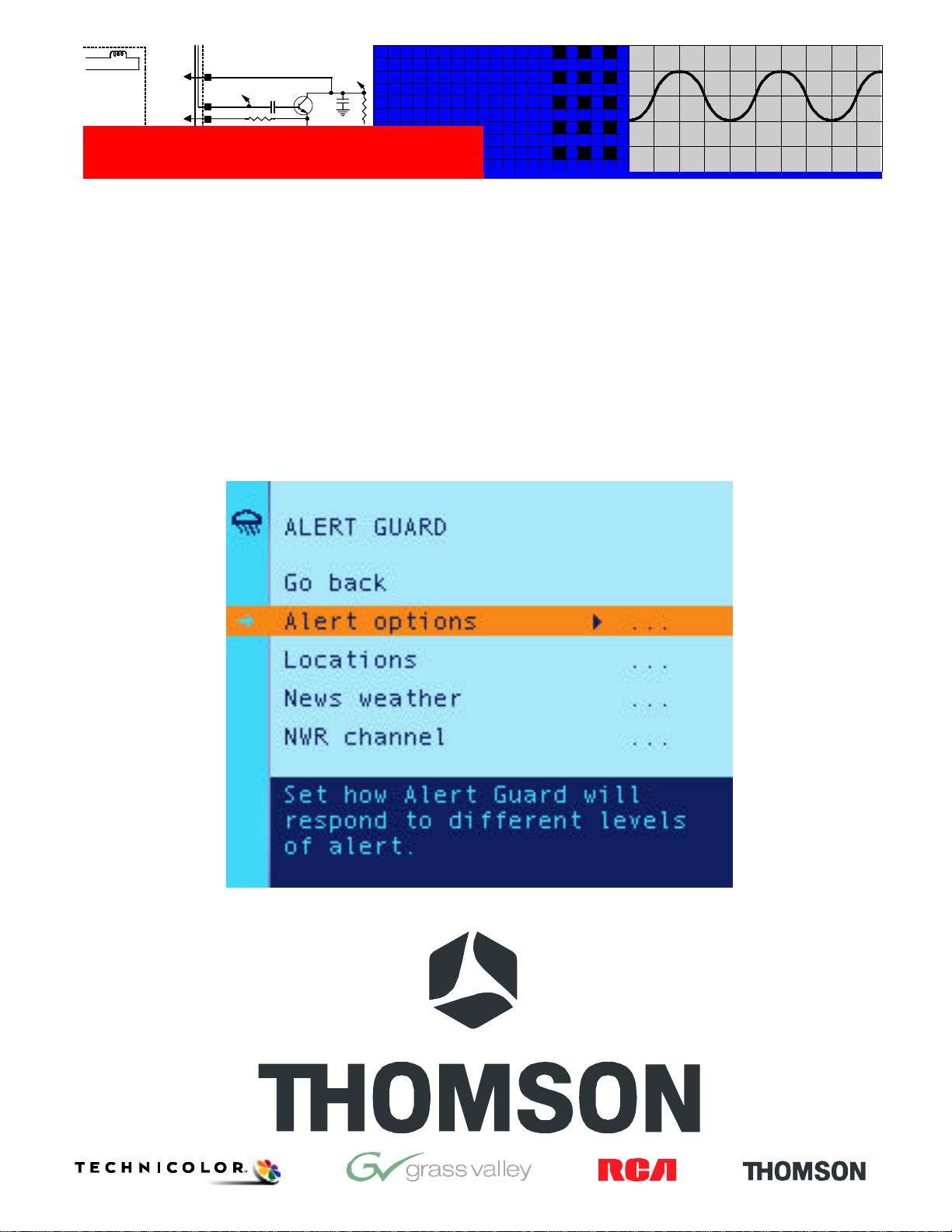
Alert Guard Menus:
• Alert Options
• Locations
• News Weather
• NWR Channel
Alert Options have to do with how the alert is sounded, type of alarm, and or text
display. These options are customized for each of the three alert types. Different
types of alarms can be set for each alert. This allows the user hear a different alarm
for each of the alert types. The alarm volume is also set independent for each alert.
Locations menu provides up to four area locations starting with My Area. My Area
is the location of the set. Areas 1-3 are used for the surrounding areas. Only areas
listed in the NWR broadcast will remain in area setup. In other words if the user lives
in Texas and selects a location in Florida, the Florida area will be removed when the
next NWR test is conducted. This is also true for adjoining counties that are covered
by different transmitters.
News Weather allows the user to select the local news weather channel to go to when
the news weather button is pressed. There are four locations the user can setup.
When the user pushes the news weather button the set will toggle through each of
the four choices, similar to a favorite channel list with only four channels.
NWR Channel sets the strongest NWR radio station received. If more then one
station is heard in the area, the strongest station will be stored. The user has the
option to manually set this to the proper station for their location.
Page 10

Customer Menus
There are five main menu items for the standard ITC008. The Alert Guard version
has an additional setup menu for Alert Guard. The five standard menu items cover
the typical customer menu options found in most TV’s. These menu options are:
• Sound
• Picture
• Setup
• Parental Control
• Time
• Alert Guard (Alert Guard equipped sets)
Sound Menu
The sound menu allows the user to customize the audio by adjusting base, treble,
and balance. Stereo mode selection includes mono, stereo, and enhanced. SAP
(secondary audio programming), internal speakers and auto volume level can be
turned on or off in the sound menu. Audio out can be set to fixed or variable.
Picture Menu
The picture menu provides the user with options to customize picture settings.
These setting include:
• Brightness
• Contrast
• Color
• Tint
• Tilt (on some sets)
Picture preset option allows the user to select from bright, natural, personal, and soft.
These settings are preset at the factory and only the personal setting can be
customized by the above adjustments. Auto color and Color warmth settings are
also included in the picture menu.
Page 11
Setup Menu
• Auto Channel Search
• List and Labels
• Closed Caption
• Auto Tuning
• Language
Parental Control
New parental controls, which work with a simple password, include a wide variety of
options including setting the maximum hours viewed per day before automatically
shutting down. The Kid Pass allows the parent to set how long the viewing time of
the set is for each day of the week. The times are set in 30 min increments and after
the set has been on for the preset length of time it will shutdown. The password will
need to be entered for set operation after the Kid Pass time has expired. Kid Pass
is only available after the time is set.
NOTE: The password can be reset if it is unknown. First make sure the TV is off.
Then simultaneously press and hold VOL< on the TV’s front panel and CLEAR on
the remote for approximately 5 seconds.
Time Menu
The time menu is used to set the correct time. This is critical for Kid Pass operation
and will be blocked by password when Kid Pass is set.
Page 12
ITC008 Chassis Layout

Overview
The ITC008 is a conventional NTSC analog color television chassis that uses the
latest integration technology to improve performance and reliability. This can be
seen with the use of an I²C-bus-controlled Ultimate One Chip (IV001) and dual audio
video switch IC IX401.
The main functions and features of IV001 are:
• System control and user interface
• Horizontal and vertical geometry processing
• Horizontal synchronization with two control loops and alignment free oscillator
• Vertical count-down circuit
• Vertical driver for DC-coupled vertical output stages
• I²C Bus control of all geometry functions
• X-ray protection
• Tuner PIF and SIF processing
• Final RGB processing and CRT pre-drive
• Alignment and setup settings for IV001 are stored in EEPROM IR01
From
+13.1Vs
From
+6.3Vs
1
2
Main CBA
Main A/V CBA
A/V
Inputs
BX07
IP30
8
9
Dual
Reg.
6
4
6
4
L
R
Alert Guard
Reset
1,2
IT03112
+7.9Vs
+3.3Vs
PO
IX402
Comb
Filter
IX401
A/V
Switch
1,2
Clk/Data
+33VrB
+5Vs2
BX01
BX01
AC in
+5Vs
9
Tuner
6
4,5
20
15
11
19
CVBS
Pr/SVHS C
Y/SVHS Y
Pb
7
6
2
Supply
ANT
FL10
11
23
PIF
Clk/Data
2,3
1
PWR ON
+3.3V VDD
61
RESET60
+3.3V VCCD Core
54,56
42
Video Out
L-Aud
R-Aud
5,6
EEPROM
Power
to Front Panel
24
KB/LED IR
46 47 48
IR01
8
BR01
6
7
IV001
TV Micro
40
7,8
41
42
+126Vs (Reg B+)
+21.5Vs & +19.5Vs
+13.1Vs
+6.3Vs
64
33
14
21
22
53
52
IF
Vid Out
38
FL50
47
IS100
MSP
46 6
+5Vs
51
4
24
25
33
+7.9Vs
Reg B+
Horiz
+7.9VsD
39
B
G
R
TS203
TS202
Vert
Mute
5
1
3
IS200
AMP
9
+19.5V
IHVT
8
10
Run
Supplies
R
L
System Block
Page 13

The integration technology can be seen in the ITC008 block diagram. The block
diagram is centered on IV001 and IR01 EEPROM. Inputs from tuner, main AV CBA,
and the front panel go to IV001. Outputs from IV001 are used to drive horizontal,
vertical, and the picture tube.
All audio and video signals enter the chassis via the Main A/V CBA. The main A/V
CBA is home to two IC’s, IX402 comb filter and IX401 audio and video switch. The
video signals passing through this board are processed and converted to RGB by
IX401. The RGB signals are passed to IV001 for further processing before being
sent to the CRT.
Switched and IF audio is processed by IS100 multi-sound processor (MSP) before
being sent to the speakers. Volume control, Stereo, balance, and tone features are
performed by IS100. Switching from tuner IF to external R/L input is also performed
by IS100. Output from IS100 (R/L) passes through mute transistors, TS202 and
TS203, on it’s way to the final amp IS200. IS200 is a 5-Watt single chip stereo amp
used to drive the internal speakers.
Alert Guard audio enters the Main A/V In CBA via BX07. IX401 routes the signal to
the speakers when selected by the user of when an alert is broadcast. Because Alert
Guard functions when the set is turned off, the audio circuit and switching are
powered by the main power supply.
The main power supply is on whenever AC power is applied to the set generating the
+126Vs (Reg B+), +21.5Vs, 19.5Vs, and +13.1Vs. The +13.1Vs is used for IP30
Dual Reg. that is switched by IV001 pin 1. This turns on the +7.9Vs providing power
to the deflection and video processing sections of IV001. The +3.3Vs is not switched
by IP30 only regulated.
Page 14

From
+13.1Vs
From
+6.3Vs
1
2
Main CBA
Main A/V CBA
A/V
Inputs
BX07
IP30
8
9
Dual
Reg.
6
4
6
4
1,2
L
R
Alert Guard
Reset
PO
Clk/Data
IT03112
+7.9Vs
+3.3Vs
IX402
Comb
Filter
IX401
A/V
Switch
1,2
+33VrB
+5Vs2
BX01
BX01
AC in
+5Vs
9
Tuner
6
4,5
20
15
11
7
19
6
2
CVBS
Pr/SVHS C
Y/SVHS Y
Pb
Power
Supply
ANT
FL10
11
23
PIF
Clk/Data
2,3
1 PWR ON
+3.3V VDD
61
RESET60
+3.3V VCCD Core
54,56
42
Video Out
L-Aud
R-Aud
5,6
EEPROM
to Front Panel
24
6 7
KB/LED IR
46 47 48
IR01
8
+126Vs (Reg B+)
+21.5Vs & +19.5Vs
+13.1Vs
+6.3Vs
BR01
64
IV001
TV Micro
Vid Out
38
40
FL50
47
IS100
41
MSP
42
7,8
46
+5Vs
IF
6 33
+7.9Vs
Reg B+
Horiz
33
+7.9VsD
14
39
21
Vert
22
B
53
G
52
R
51
4
Mute
3
TS203
24
25
TS202
5
1
IS200
AMP
9
+19.5V
IHVT
8
10
Run
Supplies
R
L
System Block
Page 15

Video 1
Video 2
Audio Out
S-Video
Audio In
Comp
Audio In
L-Out
R-Out
From
Alert Guard
MAV CBA
CV
CV
BX07
Y
C
Y
Pr
Pb
R
L
78
80
2
1
79
21
25
23
9
7
6
47
45
37
35
Clk/Data
COUT
YOUT
CVIn
686564
IX401
A/V
Switch
42,43
60
57
58
62
28
32
30
29
31
71
61
59
70
72
14
16
18
15
17
16
14
3
IX402
Comb
Filter
Chroma
PR_O/P
PB_O/P
Y
Pr
Pb
L
R
CV
Y
C
L
R
7
Y/Vout
BX03
Video 3
V-Port
TV_CVBS
Audio Out L
Audio Out R
TV-L
TV-R
BX04
FAV
S-Video
Audio In
Clk/Data
or
BX06
Sand
Castle
BX01
1
2
2
1
15
7
11
BX100
20
19
6
2
3
1
MAV Switching Block
Circuit Overview
Audio Video Processing
The A/V Processing on the ITC008 can be divided into two parts, MAV CBA
(switching) and Main Chassis (processing). The MAV CBA provides switching of
all external signals via IX401 audio video switch IC. IX401 is I2C bus controlled and
is capable of up to four switched inputs. IX402, Comb Filter, separates out the Y and
C components of the composite signal for switching by IX401. The main chassis
process the Y Pr Pb signal from IX401 using the Ultimate One Chip (IV001). The
processed RGB signal is then fed to the CRT driver.
Page 16

There are up to four external inputs connected to the main AV in CBA. These inputs
are:
• Video 1 (VID1)
• Video 2 (VID2)
• Front (FRNT)
• Component or V-Port (CVID3)
NOTE: () = OSD name for selected input. Video 1,2 and Front will display type of
video detected. i.e. Video 1 detects S-Video the display will show SVID1.
MAV CBA Switching
Video 1 and 2 are composite video (CV) with input 1 sharing S-Video. Front input
also shares S-Video with the CV input. Video 2 is shared by composite and
component video. In addition, the ITC008 can be setup for V-Port or a second
component input.
Tuner video or TV_CVBS comes from the main CBA to pin 19 of BX100 to IX401 pin
71. This CV signal is output to IX402 at pin 64 of IX401 where it is Y / C separated.
IX402 comb filter outputs the Y / C to pins 65 and 68 of IX401. The now Y / C signal
is switched and returned to the main CBA for further processing via BX06-1 (C) and
BX100-20 (Y). Corresponding audio comes form the main CBA to IX401 pins 70 and
72 via BX100 connector. The switched audio returns to the main CBA from pins 59
and 61 of IX401 for further processing and amplification. Video 1, video 2, and front
CV are also processed through IX402 while S-Video bypasses IX402.
Component video (Y Pr Pb) is switched by IX401 and output from pins 57, 58, and
62. Pin 62 of IX401 has Y signal for both component and Y / C signal. This Y/Vout
signal is sent to two pins on BX100. Pin 11 is seen by the main CBA as the Y signal
from component and pin 20 is seen by the main CBA as the Y signal from Y / C. The
selection between component and Y / C is done by IV001 on the main CBA. See
Processing for further details.
A sand castle pulse is used by IX402 for processing and timing. The signal comes
from the main CBA via connector BX06 pin 2. Connector BX01 carries the clock and
data signal from IV001 on the main CBA to IX401 pins 42 and 43. The clock and data
signal also goes to the Alert Guard module via BX07. Audio from Alert Guard is
switched by IX401 at pins 37 and 35.
Page 17

Main CBA Processing
The Y Pr Pb signals from BX100 (pins 7, 11 and 15) are connected to the RGB input
of IV001 pins 46, 47, and 48 respectively. This input becomes active when the fast
blanking signal at pin 45 is ≥ 0.8V. RGB is converted to YUV in the internal matrix,
so color saturation alignment, black stretching and de-matrix coefficient switching
can be done. Fast blanking insertion bit IN2 is high when a fast blanking signal is
detected before the end of vertical blanking (1 line). Due to this concept full-page
detection is done in an easy way.
The RGB input of the Ultimate One Chip IC can be configured as a component input.
This mode is used for models with component inputs. In component input mode, G
becomes Y input, R becomes Pr input and B become Pb input. Y input has to be
present at the external CVBS video input (pin 42) for synchronization. Component
input becomes active when pin 45 is ≥ 0.8Vdc.
The Ultimate One Chip IC decodes PAL, NTSC and SECAM signals. The PAL/
NTSC decoder needs no external reference crystals but has an internal clock
generator, which is stabilized to the required frequency by using the 12MHz clocksignal from the reference oscillator of the micro section of IV001.
Internal to IV001 video processing is a base-band delay line. The delay line is active
during NTSC to obtain a good suppression of cross color effects. The demodulated
color difference signals are internally supplied to the delay lines.
In the video section of the Ultimate One Chip, all signals are converted to YUV and
then to R-Y, G-Y, and B-Y. The R-Y, G-Y, and B-Y signal is further processed by user
controls such as contrast, brightness, and tint. Luminance delay, peaking and Black
Stretch functions are also internal.
The black stretch circuit extends the grey signal level towards the actual black level,
which is measured during burst key. The amount of extension depends on the
difference between actual black level and the darkest part of the incoming video
signal; it is thus dependent on the IRE value of the video signal.
The external CVBS video inputs are connected to IV001-42 (CVBS/Y), the internal
CVBS signal coming from tuner is coming out of IV001-38, passes the sound trap
circuit and is transmitted to pin40 via coupling capacitor. For models with SCI or MAV
board, the internal CVBS signal is connected to SCI or MAV board for switching via
pin 19 of BV001. The selected signal could be a CVBS or S-video signal. The CVBS
or Y signal is connected back to UOC via pin 20 of BV001.
Page 18

Video 1
Video 2
Audio Out
S-Video
Audio In
Comp
Audio In
L-Out
R-Out
From
Alert Guard
MAV CBA
CV
CV
BX07
Y
C
Y
Pr
Pb
R
L
78
80
2
1
79
21
25
23
9
7
6
47
45
37
35
Clk/Data
COUT
YOUT
686564
IX401
A/V
Switch
42,43
CVIn
60
57
58
62
28
32
30
29
31
71
70
72
14
16
18
15
17
61
59
16
14
3
Y
Pr
Pb
L
R
CV
Y
C
L
R
IX402
Comb
Filter
Chroma
PR_O/P
PB_O/P
Y/Vout
Video 3
V-Port
TV_CVBS
Audio Out L
Audio Out R
TV-L
TV-R
BX04
FAV
S-Video
Audio In
Clk/Data
7
BX03
or
Sand
Castle
BX01
BX06
2
1
15
7
11
BX100
20
19
6
2
3
1
1
2
+33VrB
+5Vs2
BV001
to
BX100
BR06
to
BX01
BR07
to
BX06
ANT
20
15
11
7
19
1
3
6
2
1,2
9
6
2
1
Pr
Pb
Tuner
4,5
Y
11
C
Y
FL10
23
Clk/Data
2,3
Sand Castle
34
43
42
46
47 48
TV_CVBS
TV-R
TV-L
L-Aud
R-Aud
5,6
24
PIF
IR01
EEPROM
8
IV001
TV Micro
Vid Out
38
30
31
41
42
7,8
46
IF
IS100
MSP
+5Vs
47
6 33
+7.9Vs
MAV Switching Block
B
53
G
52
R
51
440
Mute
3
TS203
24
25
TS202
5
1
8
IS200
AMP
10
9
+19.5V
R
L
Main AV Processing Block
Page 19

System Control
System control for the ITC008 is housed in the Ultimate One Chip IV001. User
interface is via IR at pin 64 and key scan at pins 6 and 7 of IV001. The UOC operates
on +3.3Vdc for system control half and 12Mhz system clock. An external EEPROM
(IR001) is used to store alignment and user setup data.
Communication with the rest of the chassis and Alert Guard is via I2C. Besides Alert
Guard, there are three devices that communicate with IV001:
• Multi-Sound Processor (IS100)
• Video IC (IX401)
• Tuner
If communication is not established with these devices, IV001 will try three times to
start and then will shutdown throwing an error code. This type of shutdown is
considered a soft shutdown and can be disabled by accessing the service mode.
When entering the service mode, acknowledgment checking is disabled allowing the
set to start in the service mode.
Because IV001 performs all major functions of the set, it is suggested great care be
taken when determining a failure with IV001. All supply voltages and pin voltages
should be checked prior to replacing IV001.
TV Off Standby TV On
AC Power
+3.3V
Reset
I2C Bus
PO Port
+8V
+5V
MSP Reset
Mute
RESET
TIME
Status
NVM
INIT
UOC
INIT
MSP
Page 20
Power On Timing

From
+13.1Vs
From
+6.3Vs
1
2
Main CBA
Main A/V CBA
A/V
Inputs
BX07
AC in
IP30
8
9
Dual
Reg.
6
4
6
4
1,2
L
R
Alert Guard
+7.9Vs
+3.3Vs
Reset
Switch
Clk/Data
IX402
Comb
Filter
IX401
A/V
1,2
+33VrB
+5Vs2
BX01
BX01
+126Vs (Reg B+)
+21.5Vs & +19.5Vs
+13.1Vs
+6.3Vs
to Front Panel
KB/LED
IV001
TV Micro
+3.3V VCCD Core
54,56
IR01
EEPROM
8
ANT
9
6
Tuner
4,5
Power
Supply
2,3
61
Clk/Data
1 PWR ON
+3.3V VDD
RESET60
5,6
System Control Block
6
7,8
BR01
7
46
+5Vs
64
IR
IS100
MSP
6 33
+7.9Vs
14
39
53
52
51
+7.9VsD
B
G
R
Page 21

Slow Start
RP037,038
DP037
CP037,038
CP039
TP020
G
DP033
15V
RP020
0.27
Ω
DP004
DP003
CP024,025
D
S
RP021
RP033
FP001
DP027
TP025
RP023
RP031
TP022
27V
RP029
RP028
DP005
RP006
DP002
RP007
DP025,026
RP132
DP023
RP027
TP023
RP026
RAW B+
RP125
DP040
27V
RP040
RP041
RP030
CP008
CP040
CP022
LP003
9
5
3
1
2
DP030
8.2V
4
3
IP001
18
16
15
14
13
12
11
10
RP155
1
2
DP080
FZP60
3.15A
FZP93
500mA
FZP61
3.15A
RP056
IP050
1
2
DP061
CP062
DP093
RP066
DP063
DP097
RP052
RP054 RP158
3
Current
CP080
Beam
Sense
DP202
CP206
CP064
Pwr Good
TP193,192
TP052
Burst
Mode
IV001 pin 63
CP094
RP151
RP057
+126V
+21.5V
+19.5V
+6.3Vs
+13.1V
PG1
DP057
9.1V
Power Supply Block
Power Supply
The ITC008 power supply is similar to the one used in the TX809 chassis. One major
difference is the ITC008 has five (5) major power supplies developed off the
secondary of LP003, 126VDC, 21.5Vdc, 13.1Vdc, 19.5Vdc and the 6.3Vdc. Secondary
regulation of the 13.1Vdc comes from IP30 dual voltage regulator producing the
standby +3.3Vs for system control. See run supply for additional information about
the +3.3Vs.
Raw B+ (150VDC) is generated by a full wave bridge rectifier (DP002/3/4/5) and is
applied to LP003, pin 9 that serves as the B+ source for the output transistor TP020.
Output transistor TP020 provides the drive to transformer LP003. The oscillator
driver circuit consists of transistors TP022, TP023 and TP025. The output of the
oscillator driver is applied to the gate of TP020 and turns on and off the output
transistor. Opto Isolator (IP001) provides the regulation feedback from the secondary
side of the supply. IP001 also provides electrical isolation between the primary and
secondary side of the supply, isolating the HOT ground from Cold ground.
By tapping a voltage from the bridge rectifier and applying it to the oscillator driver
via RP006 and RP007 initial startup is generated. The re-supply or run voltage for
the oscillator driver comes from rectifying the pulse at pin 3 of LP003 via DP025 &
DP026. The re-supply voltage is coupled back to IP001-4 via Zener DP030 and
Page 22

serves as B+ for the phototransistor in IP001. The pulse from LP003, pin 3 is also
applied to DP023 and is used to trigger the oscillator driver.
Turn off of TP020 occurs when the current through RP020 increases to the trigger
point of TP022. Once the voltage drop across RP020 rises to the predetermined
trigger point, the oscillator driver turns off, removing drive from TP020. Diode DP040
(27V zener) is used as a protective device to prevent runaway in the event of a failure
in the regulation feedback path.
IP050 (precision shunt regulator) controls or regulates IP001 (opto isolator). The
voltage applied to pin 3 determines the resistance of IP050. As the voltage on pin
3 of IP50 drops, the resistance decreases. This effectively pulls pin 2 of IP001 closer
to ground turning on the photo diode harder. This generates more light and turns on
the phototransistor harder. When the phototransistor is turned on harder, this pulls
current away from the oscillator driver circuit causing the duty cycle of the power
supply to increase (the output device stays on longer). With an increase in duty cycle,
the supply outputs more power thus raising the secondary voltages.
There are three inputs to the regulator feedback circuit (IP050, pin 3). First, the
126Vdc is monitored to regulate the standby supply whenever the television is turned
on. Second, when the set is turned off but still plugged in, +13.1Vdc is monitored to
regulate the power supply via zener DP057 and TP052. During standby (set off) the
system control microcomputer (IV001-63) outputs a Burst signal that turns on
TP052. The impedance of the standby switch circuit (TP052) is much lower than the
run regulation circuit (126Vdc). This allows the standby feedback voltage (+13.1V)
to over ride any effect the run feedback voltage (126V) might have. Third, during
operation (set on), a beam current sense voltage is applied to pin 3 of IP050. During
a high beam current situation, pin 3 of IP050 is pulled down causing pin 1 to fall. This
turns on the opto coupler harder which causes the oscillator driver to increase the
duty cycle thus pulling up the power supply. This is done to reduce the “breathing”
effect during high beam current conditions.
The standby supply has two safety shutdowns. These are over voltage and over
current shutdown. Over voltage shutdown occurs if the voltage developed at pin 3
of LP003 rises above 27 volts. Zener DP027 breaks over and shorts removing resupply and start voltages. Over current protection is provided by RP020 in the source
of TP020. Excessive current causes the voltage developed across RP020 to rise hi
enough to turn on TP022, again turning TP023 shorting gate drive of TP020 to
ground.
The ITC008 also uses circuit protectors (fuses) in the power circuits. The chart on
page 30 shows the location and power supply associated with the device.
Page 23

Power Supply
Control
IP01,IP50
DP57
9.1V
+13.1Vs
+6.3Vs
+7.9Vs
FZP66
TP52
RP153
Burst
Hi = Burst & DAM Mode
Lo = Energy Mode
+7.9Vs
63
14
IV01
+VCC
1
60
54
56
33
RP57
RP151
Pwr ON
Reset
Horiz Out
1
2
IP30
Dual
Reg.
Horiz
Drive/Out
DP36
2
IP31
1
3
8
9
RP166
6
4
TR02
Reset
Switch
LL05
CP66
DH01
33V
+5Vs
+181Vr
+3.3Vs
+33Vr
+12Vr
-12Vr
CRT
Tuner
Vertical
Switched Power Supply Block
Switched Power Supply
The switched supply consists of two (2) regulated supplies and four (4) scan derived
supplies. The regulated supplies are +7.9Vs and +5Vs. IP30 (dual voltage regulator)
produces the +7.9Vs and the +3.3Vs. The +5Vs is derived from IP31 (5V Reg) that
is fed by the switched +7.9Vs. The non-switched +3.3Vs from pin 9 of IP30 is active
as long as the +6.3Vs is present at pin 1. The +3.3Vs is used for IV01 (System
Control) reset (IP30-6) and VCC pin 54,56.
The switched voltage from IP30 pin 8 (+7.9Vs) is activated when pin 4 goes high from
the power on (IV01 pin 1). The Burst (High) from IV01-63 turns on TP52 increasing
the stand-by supply current to compensate for the additional load during power up.
When IP30 gets the power on signal, +7.9Vs from pin 8 gets applied to pin 14 of IV01
supplying B+ for Horizontal drive. Horizontal drive from IV01 pin 33 drives the driver
/ Output stage of horizontal. The output stage drives LL05 producing four (4) scan
derived supplies. The +181Vr is used for CRT drive and supplying DH001 (33V
Zener). DH001 and it’s associated circuit produce the tuner voltage +33Vr. Vertical
+ and – 12Vr are also developed by LL05.
Page 24

DL62
CL30
DL30
+7.9VsA
CL35
RV73
TL31
RL36
+13.1Vr
+7.6VsD
TL060/061
Bias
TL33
RL37
RL38
14
33 Hout
IV001
EHT
TL62
LL32
3
1
RL34
DL35
+12Vr 6
Vcc
36
34
from
Pincushion
CBA
+7.6VsE
XRP
DZ01,03,05
RL68
TL35
6
4
BL005
BL003
123
TZ01
Feed Back
RL63
RL07
CL21
CL23,25,26
RL25,26
DL25 LL26
Horiz
Yoke
+126V
Pin 12
LL05
DL21
5
1
LL05
Pin 8
LL05
IHVT
13
12
10
11
BF001
3
to
2
Pincushion
1
CBA
Anode
Focus
Screen
TL50
8
RL12
7
RL10
RL40
9
DL40
CL41
Buffer
Heater & XRP
Htr Return
DL12
DL10
LL40
RL41
to 44
from
RL06
RF07
Beam Current
Sense to PWR
IP050-3
+12Vr
CL13
-12Vr
CL11
+181Vr
+33Vr
DL01
33V
Horizontal Block
Horizontal Deflection
Horizontal deflection starts with drive from IV001 pin 33. Drive is produced when the
+7.6Vsd is present at pin 14 of IV001. The drive signal is coupled to TL31 via RV73
and CL30. The +13.1Vr provides B+ to TL31 and TL33 until the +12Vr comes up and
re-supplies the B+. LL32 couples the drive signal to the output TL35. TL35 drives
the fly-back transformer LL05, producing the scan-derived voltages. Feed back from
pin 12 of LL05 is used as a slow start bias for TL31 and TL33.
The horizontal output signal is generated by means of an oscillator that is running
at 25Mhz and is stabilized with 12Mhz reference. A digital control circuit that is locked
to the reference signal of the color decoder determines the free running frequency
of the oscillator. When IV001 is switched-on the horizontal output signal is
suppressed and the oscillator is calibrated. When all sub-address bytes have been
sent via I²C bus to IV001 and the frequency of the oscillator is correct, the horizontal
drive signal is switched on. To obtain a smooth switching on and switching off of the
horizontal output stage, an internal soft start/stop function is used. To protect the
horizontal output transistor, the horizontal drive is immediately switched off when a
power on reset is detected.
Page 25

IV001 has a second control loop to guarantee the drive pulse for the horizontal output
stage. The horizontal output is gated with the fly-back reference pulse (LFB pin 34),
so that the horizontal output transistor cannot be switched on during that time.
All geometry alignments are done via I²C bus commands except E/W alignment. Xray protection is activated via EHT tracking (IV001 pin 36) when the level exceeds
+3.9V. If the level exceeds +3.9V at pin 36, horizontal drive will be stopped at pin
33 shutting down horizontal drive and the set.
The horizontal drive output is an open collector configuration. Thus an AC coupled
Darlington driver (TL31 and TL32) is used. Before startup, the capacitor CL35 is
charged by +13.1Vr via RL37 and RL38. When the H drive signals are starting the
T-on time is very short and the energy stored in CL35 is enough to supply the driver.
Because the +12Vr supply is generated in forward mode the first pulses charge
CL13. Once CL13 is charged the supply voltage for the driver is coming from the
+12Vr via DL35 and RL 34.
E/W Correction
An external E/W correction-driving signal is produced by making use of synchronized
vertical feedback signal derived from RF07 off pin 2 of BF001. The saw tooth is
amplified and inverted before being fed into an integrator (IL101) to generate a
parabola signal. PL141 acts as an E/W amplitude control by controlling the parabola
signal amplitude. PL140 is part of the voltage divider that determines the DC level
used for horizontal size alignment. The horizontal breathing is controlled by the
beam current information via RL150 to the DC level biasing at PL140. The trapezium
alignment is achieved by introducing the inverted saw tooth waveform to the
parabola output signal.
A safety circuit RL112, RL113, DL113 DL114, CL110, CL114, CL123, RL110,
DL117, DL118, RL117, RL118, and DL119 is to inhabit the H-drive and shut down
the deflection circuit in the case of TL101 failure.
A diode modulator (DL21, CL21 (main CBA), DL121, DL122 and CL122 (Pincushion
CBA) is used to modulate the horizontal deflection current with vertical frequency in
order to obtain higher amplitude of deflection current in the middle and smaller
amplitude on the top and bottom of the raster.
The resonant frequency LC product of bridge coil LL122 and CL122 in series
connected with CL123 is the same as the product of tuning capacitor CL21 together
with the deflection yoke. The capacitive divider CL21 and CL122 produces a retrace
voltage across CL122. The integrated value of this voltage is corresponded by the
Page 26

voltage across CL123. A maximum voltage across CL123 means the deflection
current is minimal and vice versa.
DL62
CL30
DL30
+7.9VsA
CL35
RV73
TL31
RL36
+7.6VsD
TL62
RL63
RL07
TL060/061
Bias
TL33
RL37
LL32
3
1
RL34
TL35
6
4
RL68
CL21
CL23,25,26
RL25,26
DL21
DL25 LL26
RL38
DL35
BL005
+126V
Horiz
Yoke
Pin 12
LL05
+12Vr 6
+13.1Vr
33 Hout
14
IV001
EHT
Vcc
36
34
Pincushion
from
CBA
+7.6VsE
XRP
DZ01,03,05
BL003
123
TZ01
Feed Back
5
1
LL05
Pin 8
LL05
IHVT
BF001
3
to
2
Pincushion
1
CBA
Anode
13
from
RL06
RF07
Focus
Screen
Beam Current
TL50
8
12
11
RL12
Buffer
Heater & XRP
Htr Return
DL12
Sense to PWR
IP050-3
+12Vr
CL13
RL10
RL40
DL40
CL41
DL10
LL40
RL41
to 44
CL11
DL01
33V
-12Vr
+181Vr
+33Vr
7
10
9
RL150
BL101
3
2
1
PL143
+12.2Vpin
RL134
RL106
RL131
RL105
RL104
RL134
PL140
RL132
RL137
RL136
RL133
RL108
RL107
Horizontal Block
DL138
RL138
CL138
IL101
3
2
6
5
9
10
12
13
1
7
8
14
RL145
PL141
DL117
RL118
RL117
CL144
RL144
TL101
RL141
DL118
RL111
RL112
RL113
47V
DL119
DL114
+12.2Vpin
LL122
CL122
DL122
RL114
DL113
CL114
CL123
DL121
BL103
3
2
1
RL110
CL110
to
CL021
and
DL021
E/W Correction Block
Page 27

Vertical Deflection
The ITC008 vertical deflection circuit consists of vertical ramp generator in IV001
processor and a power stage IF001. The vertical ramp generator is in the TV
processor IV001. The geometry parameters can be adjusted via the I2C bus to
control TV processor IV001. Four parameters Vertical Slope, Vertical Amplitude,
Vertical Shift and S Correction are all controlled by software.
The power stage, IF001, is configured as differential amplifier and driven by the ramp
current delivered by IV001 pin 21 and pin 22. The vertical ramp current (Ir) is imposed
on the V-drive signals. So we have I+Ir and I-Ir from pin 21 and pin 22 respectively.
The fly-back supply voltage on pin 5 is 2 x Vsupply + |-Vsupply| and the maximum
scanning supply voltage on pin 5 is Vsupply or -Vsupply. Pin 3 voltage is at -Vsupply
and CF10 is charged to Vsupply + |-Vsupply| during scanning period. The fly-back
generator switches pin 3 to Vsupply. Thus the total fly-back supply voltage is: 2 x
Vsupply + |-Vsupply|.
CF08/09-RF08 is the zero-pole compensation to increase the phase margin of the
amplifier while still maintaining expected bandwidth. RF08 is a fusible resistor to
prevent overheating in the event of CF08/09 failure. This circuit also helps to protect
the IC during picture tube arcing. DF01 also protects the vertical IC during picture
tube arcing.
Resistor RF09 damps spurious oscillation in the VDC and reduces crosstalk from the
HDC into the VDC.
RF07 is a current sensing resistor. The deflection current is proportional to the output
voltage across RF07.
RF101, DF101, DF102, RF102 and CF101 act as a protection circuit to pull down the
Beam Current Limit path as to suppress the video amplitude during vertical booster
IC failure. This prevents CRT screen phosphor from burning by intense white line.
Page 28

+7.9Vs
Vcc
BF001
RF06
IV001
VDriveB
14
VDriveA
RV06
21
DF02
22
RV05
DF03
RF02
RF03
RF04
1
7
4
CF05
PWR
AMP
2 6 3
DF10
Vertical Output
CF10
IF001
5
DF01
56V
Pincushion
RF08
to
BF002
RF09
CF09
RF07
CF08
-12Vr
DF101
+12Vr
DF102
Vertical Block
RF101
CF101
RF102
-12Vr
Beam Current Limit
Page 29

Shutdown
The ITC008 is a basic chassis with a few protection fuses and a shutdown circuit.
Shutdown consists of an XRP circuit that monitors the heater pulse from pin 12 of
LL05. A detector circuit consisting of DZ01, DZ03, DZ05, and 1% resistors (RZ05
and RZ07) determine the trip point of TZ01. If the heater pulse is too high, TZ01 turns
on increasing the voltage at pin 36 of IV001 (>3.9Vdc). IV001 in turn shuts down
horizontal drive turning off the set.
Aside from the above listed shutdown the ITC008 also uses circuit protectors (fuses)
in the power circuits. The below chart shows the location and power supply
associated with the device.
Device
(Open)
FP01 (AC Fuse)
Main CBA
FZP60 (+21.5V)
Main CBA
FZP61 (+13.1V)
Main CBA
FZP66 (+7.9V)
Main CBA
FZP93 (+6.3V)
Main CBA
FZK001 (+13.1V)
Alert Guard
FZX001 (+12V)
MAV
Reg B+
0Vdc NO NO NO DEAD
132Vdc YES YES NO Set comes on with No Audio
0Vdc NO NO NO
132Vdc NO NO NO Cycles when Power is pushed
125Vdc NO NO NO Dead, Power supply working
132Vdc NO NO NO
128Vdc YES NO Yes OSD present on channel change
High
Voltage
Video Audio Comments
DP27 Shorts (Over Voltage
protect)
Dead, Disconnect Alert Guard
module and set powers on with
video and audio.
Circuit Protection Chart
Page 30

Horiz
Driver
Ckt
LL05
IHVT
DL21
CL21
LL32
3
1
TL35
6
4
Horiz
Yoke
+126V
5
1
13
8
11
12
Anode
Focus
Screen
Htr Return
Heater & XRP
33
Hout
Vcc
IV001
EHT
14
36
RV70
RV71
+7.6VsE
RV77
DZ03
10V
TZ01
RZ09
RZ11DZ05
RZ05
1%
RZ07
1%
XRP Block
RZ03
XRP1
XRP2
RZ01
6
7
DZ01
Page 31

Troubleshooting Section
Dead Set Troubleshooting
Symptom: Nothing happens when power is pushed, set is dead.
NOTE 1: DP027 will short during over voltage, shutting down the power supply. IF
DP027 is shorted, check FZP61. If FZP61 is open, check the +13V for excessive
load. A loss of feedback will cause over voltage condition.
NOTE 2: Disconnect Alert Guard CBA. A problem with alert guard can cause
the set to appear dead!
1. Check RAW B+, if not OK check the full wave bridge rectifier DP002/003/004/
005 and it’s associated components.
2. If RAW B+ OK, check the current sensing resistor RP020. If open, this
indicates there has been a severe over current condition in the power supply
and all active components on the primary side of LL003 should be checked
and replaced (See note 3 in step 6).
3. Check DC voltage and waveform on the gate of TP020. This will indicate if
the oscillator is running and the power supply is working.
4. If there is no waveform on the gate of TP020, unsolder the drain of TP020 and
check for 7.9Vdc on the gate. 7.9Vdc on the gate of TP020 indicates startup circuit is working go to step 6. If waveform present on the gate of TP020,
the power supply is working, troubleshoot system control.
5. If DC on gate of TP020 is not 7.9Vdc, check TP025, DP027, DP023, RP006,
and RP007 (start up circuit) and replace if suspect.
6. If no waveform on gate of TP20 (DC OK), check TP22, TP23 and their
associated components. Replace all transistors if one has failed or is
suspect.
NOTE 3: If TP020 has failed more than likely the other transistors have been
stressed and the circuit will self-destruct again when plugged into 120 AC
unless all active components are replaced.
7. If TP020 checks OK (with primary circuit pulsing), check IP01 (Ref Reg) and
IP50 (Opto Coupler) and their associated components.
Page 32

Slow Start
RP037,038
DP037
CP037,038
CP039
3
TP020
G
DP033
15V
RP020
0.27
5
Ω
CP024,025
D
S
RP021
RP033
2
FP001
DP004
DP003
DP027
RP031
27V
TP025
RP023
RP029
RP028
TP022
DP005
RP006
DP002
RP007
DP025,026
RP132
DP023
RP027
TP023
RP026
4
1
9
5
3
1
2
DP030
8.2V
4
3
LP003
IP001
18
16
15
14
13
12
11
10
RP155
1
2
FZP60
3.15A
FZP61
RP125
DP040
27V
RP040
RP041
RAW B+
CP008
RP030
CP040
CP022
6
Power Supply Block
DP080
FZP93
500mA
3.15A
RP056
IP050
1
2
DP061
CP062
DP093
RP066
DP063
DP097
RP052
RP054 RP158
3
Current
CP080
Beam
Sense
DP202
CP206
CP064
Pwr Good
TP193,192
TP052
Burst
Mode
IV001 pin 63
CP094
RP151
RP057
+126V
+21.5V
+19.5V
+6.3Vs
+13.1V
7
PG1
DP057
9.1V
Device
(Open)
FP01 (AC Fuse)
Main CBA
FZP60 (+21.5V)
Main CBA
FZP61 (+13.1V)
Main CBA
FZP66 (+7.9V)
Main CBA
FZP93 (+6.3V)
Main CBA
FZK001 (+13.1V)
Alert Guard
15.6V p-p
10uS/Div 57.14Khz
Reg B+
0Vdc NO NO NO DEAD
132Vdc YES YES NO Set comes on with No Audio
0Vdc NO NO NO
132Vdc NO NO NO Cycles when Power is pushed
125Vdc NO NO NO Dead, Power supply working
132Vdc NO NO NO
High
Voltage
Video Audio Comments
DP27 Shorts (Over Voltage
protect)
Dead, Disconnect Alert Guard
module and set powers on with
video and audio.
FZX001 (+12V)
MAV
128Vdc YES NO Yes OSD present on channel change
Circuit Protection Chart
Page 33

Shutdown Troubleshooting
Symptom: Set is pulsing when power is pushed wont start.
NOTE: Using Chipper Check, check for error codes. This will indicate which device
maybe causing the shutdown.
Remember to ALWAYS reset the error codes and allow the set to cycle again to
obtain a current error code reading.
Disconnect Alert Guard CBA. A problem with alert guard can cause the set to
appear dead!
1. With the set plugged into AC power check for +126Vdc on TL035-C horizontal
output transistor. If missing see dead set troubleshooting, if present, power
supply is working.
2. Push the power switch, if set pulses then system control is working.
3. With set pulsing, check for horizontal drive at pin 33 of IV001. If not present
suspect IV001 and it’s associated circuits.
4. Waveform present at pin 33 of IV001 indicates IV001 and system control are
working and problem is in the horizontal circuit. Troubleshoot horizontal
circuit.
Page 34

+7.9VsA
DL62
CL30
DL30
4.7Vp-p
3
RL36
CL35
+7.6VsD
RV73
TL060/061
TL31
+13.1Vr
TL62
Bias
TL33
LL32
3
1
RL37
RL34
RL38
33 Hout
IV001
DL35
+12Vr 6
Vcc
14
36
EHT
34
from
Pincushion
CBA
+7.6VsE
XRP
DZ01,03,05
RL68
TL35
6
4
BL005
BL003
123
TZ01
Feed Back
RL63
RL07
DL21
CL21
CL23,25,26
RL25,26
DL25 LL26
Horiz
Yoke
+126V
Pin 12
LL05
LL05
+126Vdc
5
1
Pin 8
LL05
1
IHVT
13
12
10
11
BF001
3
to
2
Pincushion
1
CBA
Anode
Focus
Screen
TL50
8
RL12
7
RL10
RL40
9
DL40
CL41
Buffer
Heater & XRP
Htr Return
DL12
DL10
LL40
RL41
to 44
from
RL06
RF07
Beam Current
Sense to PWR
IP050-3
+12Vr
CL13
-12Vr
CL11
+181Vr
+33Vr
DL01
33V
Horizontal Block
Page 35

Horizontal Troubleshooting
Symptom: No high voltage horizontal wont start
1. Unsolder collector of TL35 (HOT).
2. Monitor the base of TL35 and push the power switch. The set will cycle until
power is pushed again and a horizontal pulse will be present at the base of
TL35 while it is cycling.
3. If pulse is present on the base of TL35, IV001 and the driver circuit is working.
The problem is off the collector of TL35. Suspect Yoke, Yoke return circuit,
pincushion, LL05 and the secondary side of LL05.
4. If pulse is missing or set won’t cycle suspect IV001, TL31, TL33, LL32 and
their associated circuits.
+7.9VsA
DL62
CL30
DL30
4
4.7Vp-p
RL36
CL35
+7.6VsD
RV73
TL060/061
TL31
+13.1Vr
TL62
RL63
RL07
Bias
TL33
RL37
RL38
+12Vr 6
Vcc
14
33 Hout
IV001
36
EHT
34
2
LL32
3
1
RL34
DL35
Pincushion
XRP
RL68
TL35
6
4
BL005
BL003
123
from
CBA
+7.6VsE
TZ01
DZ01,03,05
Feed Back
CL21
CL23,25,26
DL25 LL26
RL25,26
Horiz
Yoke
+126V
Pin 12
1
DL21
5
1
LL05
Pin 8
LL05
LL05
IHVT
BF001
3
to
2
Pincushion
1
CBA
Anode
13
8
12
11
7
10
9
DL40
CL41
RL12
RL10
RL40
Focus
Screen
TL50
Buffer
Heater & XRP
Htr Return
DL12
DL10
LL40
RL41
to 44
from
RL06
RF07
Beam Current
Sense to PWR
IP050-3
+12Vr
CL13
-12Vr
CL11
+181Vr
+33Vr
DL01
33V
3
Page 36
Horizontal Block

System Control Troubleshooting
Before replacing IV001 these series of checks need to be performed.
1. Check DC voltage on pins 2, 3 (4.5Vdc), 54, 56, 58, 59, 61(3.3Vdc) and 61
(0Vdc). These pins are used for system control function. If missing
troubleshoot the appropriate circuit area.
2. Check pins 6, 7, and 64 for 3.3Vdc. These pins are user interface inputs. If
missing or low troubleshoot the appropriate circuit area.
3. Check pins 12, 18, 30, 41, and 57 for ground. Improper ground to IV001 can
cause erratic operation.
+6.3Vs
From
+13.1Vs
From
IP30
Dual
Reg.
1
2
Main CBA
Main A/V CBA
A/V
Inputs
BX07
R
Alert Guard
4
AC in
6
L
8
9
6
4
1,2
+7.9Vs
+3.3Vs
Reset
Switch
Clk/Data
IX402
Comb
Filter
IX401
A/V
1,2
+33VrB
+5Vs2
BX01
BX01
54,56
IR01
EEPROM
+126Vs (Reg B+)
+21.5Vs & +19.5Vs
+13.1Vs
+6.3Vs
to Front Panel
6 7
KB/LED
IV001
TV Micro
58,59
1
8
ANT
9
6
Tuner
4,5
Power
Supply
2,3
1 PWR ON
61
+3.3V VCCD Core
5,6
Clk/Data
+3.3V VDD
RESET60
System Control Block
BR01
64
IR
GND
12,18,30,41,57
IS100
MSP
7,8
46 6
+7.9Vs
+5Vs
2
14
+7.9VsD
39
B
53
G
52
R
51
3
33
Page 37

TITC0081
 Loading...