

Raytheon RMWW12001 Datasheet
Raytheon RF Components
362 Lowell Street
Andover, MA 01810
Revised March 2, 2001
Page 1
www.raytheon.com/micro
Characteristic performance data and specifications are subject to change without notice.
PRODUCT INFORMATION
Description
u 4 mil substrate
u Conversion loss 10 dB (typ.)
u No DC bias required
u Chip size 1.5 mm x 2.5 mm
Features
The RMWW12001 is a 12 to 24 GHz Doubler designed to be used in the LO chain of point to point radios, point to
multi-point communications, LMDS, and other millimeter wave applications. In conjunction with other Raytheon
amplifiers, multipliers and mixers it forms part of a complete 23 and 26 GHz transmit/receive chipset. The
RMWW12001 utilizes Raytheon’s 0.25 µm power PHEMT process and is sufficiently versatile to serve in a variety
of multiplier applications.
RMWW12001
12-24 GHz Doubler MMIC
Electrical
Characteristics
(At 25ºC),
50Ω system,
Pin=+18 dBm
Parameter Min Typ Max Unit
Input Frequency Range 8.5 12 GHz
Output Frequency Range 17 24 GHz
Input Drive Power +16 +18 dBm
Conversion Loss 10 12.5 dB
Conversion Loss Variation
vs. Frequency 2 dB
Parameter Min Typ Max Unit
Fundamental Rejection -20 dBc
3rd Harmonic Rejection -25 dBc
4th Harmonic Rejection -25 dBc
5th Harmonic Rejection -35 dBc
Input Return Loss
(Pin = +18 dBm) 12 dB
Absolute
Maximum
Ratings
Parameter Symbol Value Units
RF Input Power (from 50 Ω source) P
IN
+22 dBm
Operating Baseplate Temperature T
C
-30 to +85 °C
Storage Temperature Range T
stg
-55 to +125 °C
CAUTION: THIS IS AN ESD SENSITIVE DEVICE.
Chip carrier material should be selected to have GaAs compatible thermal coefficient of expansion and high thermal
conductivity such as copper molybdenum or copper tungsten. The chip carrier should be machined, finished flat,
plated with gold over nickel and should be capable of withstanding 325°C for 15 minutes.
Die attachment should utilize Gold/Tin (80/20) eutectic alloy solder and should avoid hydrogen environment for
PHEMT devices. Note that the backside of the chip is gold plated and is used as RF ground.
These GaAs devices should be handled with care and stored in dry nitrogen environment to prevent contamination
of bonding surfaces. These are ESD sensitive devices and should be handled with appropriate precaution including
the use of wrist grounding straps. All die attach and wire/ribbon bond equipment must be well grounded to prevent
static discharges through the device.
Recommended wire bonding uses 3 mils wide and 0.5 mil thick gold ribbon with lengths as short as practical
allowing for appropriate stress relief. The RF input and output bonds should be typically 0.012” long corresponding
to a typically 2 mil between the chip and the substrate material.
Application
Information
Step 1: The RMWW12001 does not require DC bias.
Apply RF input signal at the appropriate
frequency band and input drive level.
Step 2: Follow turn-off sequence of:
Turn off RF input power.
Recommended
Procedure for
Operation
The following sequence of steps must be followed to properly test the amplifier:
Raytheon RF Components
362 Lowell Street
Andover, MA 01810
Revised March 2, 2001
Page 2
www.raytheon.com/micro
Characteristic performance data and specifications are subject to change without notice.
PRODUCT INFORMATION
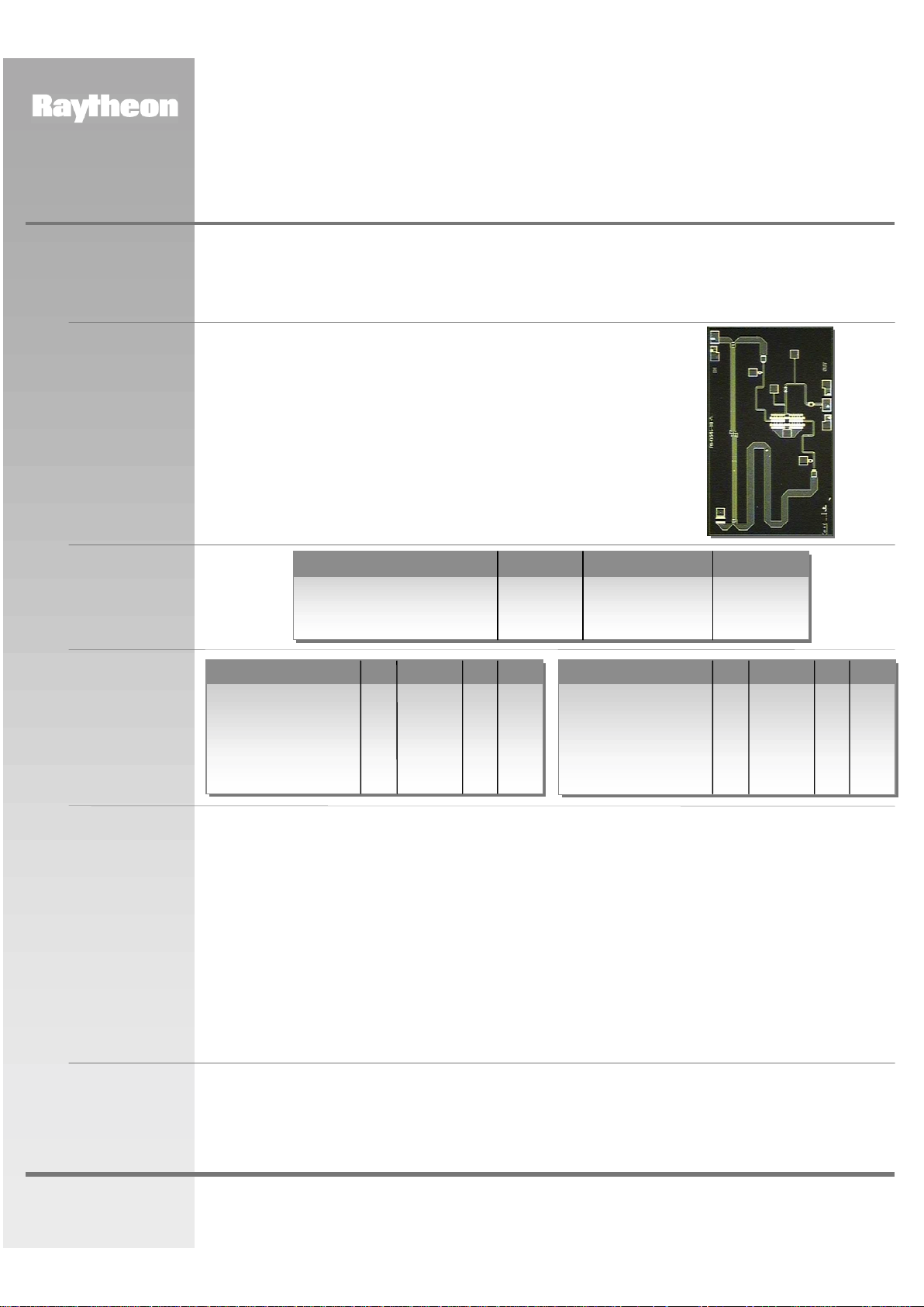
Figure 2
Chip Layout and Bond
Pad Locations
Chip Size is 1.5 mm x
2.5 mm 100 µm. Back
of chip is RF ground
Dimensions in mm
0.0
0.0
0.0
0.0
1.5
1.5
2.5 2.5
2.345
2.2025
1.4035
1.56
1.7165
MMIC Chip
RF OUTRF IN
Ground
(Back of Chip)
X2
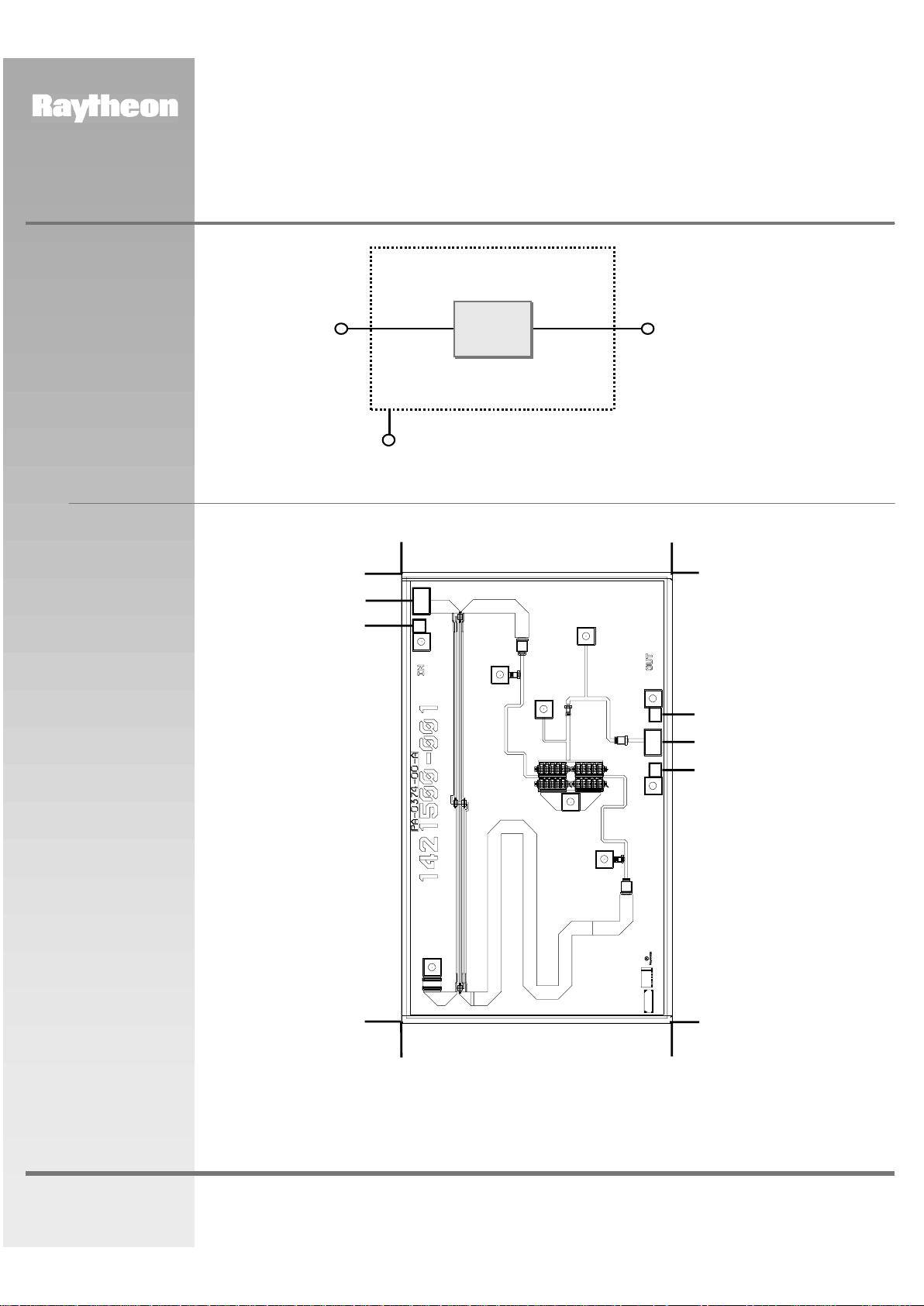
Figure 1
Functional Block
Diagram
RMWW12001
12-24 GHz Doubler MMIC
 Loading...