

Raytheon RMWB11001 Datasheet
RMWB11001
11 GHz Buffer Amplifier MMIC
PRODUCT INFORMATION
Description
Features
Absolute
Maximum
Ratings
The RMWB11001 is a 2-stage GaAs MMIC amplifier designed as a 10.5 to 11.7 GHz Buffer Amplifier for use in the
LO chain of point to point radios, point to multi-point communications, LMDS, and other millimeter wave
applications. In conjunction with other Raytheon amplifiers, multipliers and mixers it forms part of a complete 38
GHz transmit/receive chipset. The RMWB11001 utilizes Raytheon’s 0.25µm power PHEMT process and is
sufficiently versatile to serve in a variety of medium power amplifier applications.
4 mil substrate
Small-signal gain 21 dB (typ.)
Saturated power out 19 dBm (typ.)
Voltage detector included to monitor Pout
Chip size 2.0 mm x 1.3 mm
Parameter Symbol Value Units
Positive DC voltage (+4 V Typical) Vd +6 Volts
Negative DC voltage Vg -2 Volts
Simultaneous (Vd - Vg) Vdg 8 Volts
Positive DC Current I
RF Input Power (from 50 Ω source) P
Operating Baseplate Temperature T
Storage Temperature Range T
Thermal Resistance (Channel to Backside) R
D
IN
C
stg
jc
104 mA
+8 dBm
-30 to +85 °C
-55 to +125 °C
180 °C/W
Electrical
Characteristics
(At 25°C), 50 Ω
system, Vd=+4 V,
Quiescent Current
Idq=36 mA
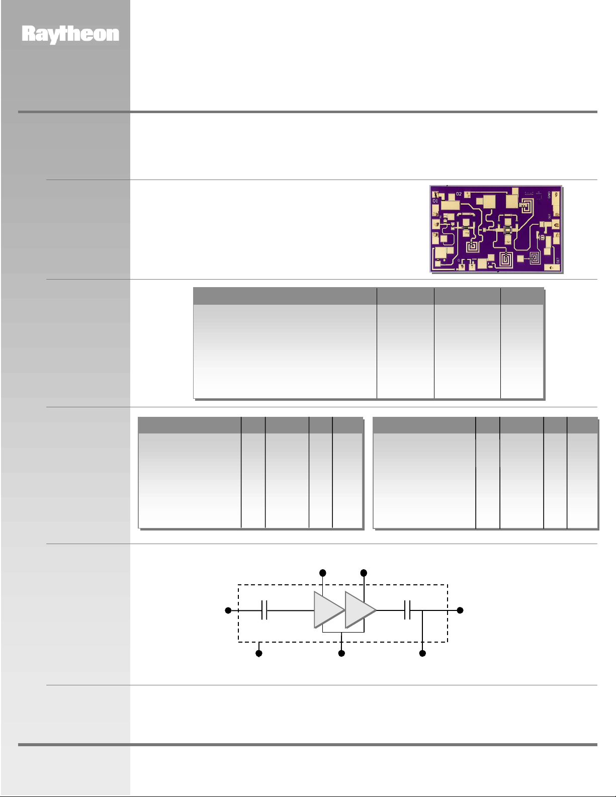
Functional
Block Diagram
Parameter Min Typ Max Unit
Frequency Range 10.5 11.7 GHz
Gate Supply Voltage
Gain Small Signal
(Pin=-10 dBm) 18 21 dB
Gain Variation vs. Frequency 0.5 dB
Power Output Saturated:
(Pin=2 dBm) 17 19 dBm
Drain Current at Psat
(Pin=2 dBm) 55 mA
2
Notes:
1. Typical range of gate voltage is -0.8 to -0.2V to set Idq of 36 mA.
Detector delivers approx. 0.5V DC into 3k Ω load resistor for >+18 dBm output power. If output power level detection is not
2.
desired, do not make connection to detector bond pad.
Characteristic performance data and specifications are subject to change without notice.
1
(Vg) -0.5 V
Drain Supply
Vd1
MMIC Chip
RF IN RF OUT
Ground
(Back of Chip)
Gate Supply
Vg
Parameter Min Typ Max Unit
Power Added Efficiency
Input Return Loss
Output Return Loss
Noise Figure 4 dB
Detector Voltage
Drain Supply
Vd2
(PAE): at Psat 35 %
(Pin=-10 dBm) 13 dB
(Pin=-10 dBm) 18 dB
(Pout=+18 dBm) 0.5 V
Output Power
Detector Voltage Vdet
www.raytheon.com/micro
Revised March 14, 2001
Page 1
Raytheon RF Components
362 Lowell Street
Andover, MA 01810
RMWB11001
11 GHz Buffer Amplifier MMIC
PRODUCT INFORMATION
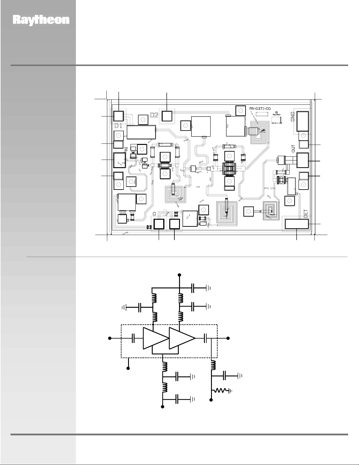
Figure 1
Chip Layout and
Bond Pad Locations
Chip Size is 2.0 mm
x 1.3 mm x 100
Back of chip is RF
and DC ground
µm.
Dimensions in mm
0.0
0.11
1.3
1.145
0.873
0.720
0.567
0.0
0.0
0.577
0.5
0.65 1.828
2.0
1.3
0.873
0.720
0.567
0.106
0.0
2.0
Figure 2
Recommended
Application Schematic
Circuit Diagram
Drain Supply
Vd=+4 V
L = Bond Wire
Inductance
100pF 100pF
LL
LL
10,000pF
RF OUTRF IN
MMIC Chip
L
Ground
(Back of Chip)
Gate Supply
Vg
Characteristic performance data and specifications are subject to change without notice.
100pF
L
10,000pF
L
Output Power
Detector Voltage
Vdet
100pF
3 k
Ω
Note: Detector delivers approx.
0.5V DC into 3k Ω load resistor for
>+18 dBm output power. If output
power level detection is not
desired, do not make connection to
detector bond pad.
www.raytheon.com/micro
Revised March 14, 2001
Page 2
Raytheon RF Components
362 Lowell Street
Andover, MA 01810
 Loading...