

Raytheon RMTR13390 Datasheet
Raytheon RF Components
362 Lowell Street
Andover, MA 01810
Revised April 6, 2001
Page 1
www.raytheon.com/micro
Characteristic performance data and specifications are subject to change without notice.
ADVANCED INFORMATION
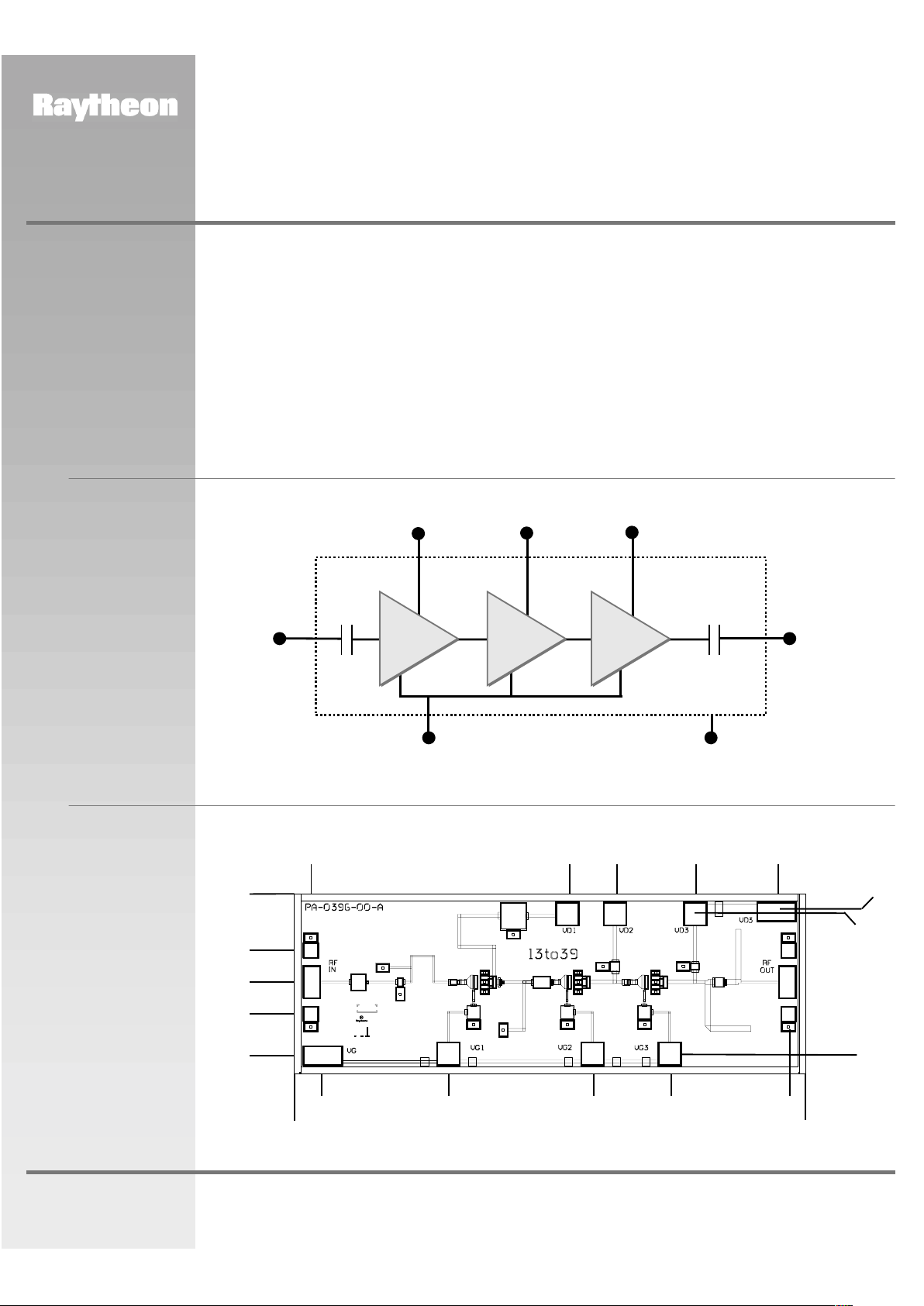
The RMTR13390 is a 13 to 39 GHz Tripler designed to be used in the LO chain of point to point radios, point to
multi-point communications, LMDS, and other millimeter wave applications. The RMTR13390 is a three stage
amplifier in which the first stage acts as a harmonic generator followed by two stages of amplification at 3Fo. The
RMTR13390 utilizes Raytheon’s advanced 0.15 µm gate length PHEMT process and is sufficiently versatile to
serve in a variety of multiplier applications.
Description
2 mil substrate
Conversion Loss 5 dBm (typ.)
Wide operating bandwidth
Chip size 3.224 mm x 1.134 mm
Features
Electrical
Characteristics
(At 25°C), 50 Ω system,
Vd = +5 V, Quiescent
current (Idq)= 100 mA,
Pin=+17 dBm
Note: 1. Typical range of the negative gate voltage is -0.5 to 0.0V to set typical Idq of 100 mA.
Absolute
Maximum
Ratings
Parameter Symbol Value Unit
Positive DC Voltage (+5 V Typical) Vd + 6 Volts
Negative DC Voltage Vg - 2 Volts
Simultaneous (Vd - Vg) Vdg + 8 Volts
Positive DC Current Id 187 mA
RF Input Power (from 50 Ω source) P
IN
+22 dBm
Operating Baseplate Temperature T
C
-30 to +85 °C
Storage Temperature Range T
stg
-55 to +125 °C
Thermal Resistance R
j
117 °C/W
(Channel to Backside)
Parameter Min Typ Max Unit
Input Frequency Range 12 13.5 GHz
Output Frequency Range 36 40.5 GHz
Gate Supply Voltage (Vg)
1
- 0.2 V
Input Drive Power @ Fo +15 +17 dBm
Output Power @ 3Fo +12 dBm
Parameter Min Typ Max Unit
Conversion Loss 5 dBm
Fundamental Rejection -15 dBc
2nd Harmonic Rejection -25 dBc
4th Harmonic Rejection -25 dBc
Input Return Loss 8 dB
Output Return Loss 7 dB
RMTR13390
13-39 GHz Tripler MMIC
Raytheon RF Components
362 Lowell Street
Andover, MA 01810
Revised April 6, 2001
Page 2
www.raytheon.com/micro
Characteristic performance data and specifications are subject to change without notice.
ADVANCED INFORMATION
CAUTION: THIS IS AN ESD SENSITIVE DEVICE.
Chip carrier material should be selected to have GaAs compatible thermal coefficient of expansion and high thermal
conductivity such as copper molybdenum or copper tungsten. The chip carrier should be machined, finished flat,
plated with gold over nickel and should be capable of withstanding 325°C for 15 minutes.
Die attachment should utilize Gold/Tin (80/20) eutectic alloy solder and should avoid hydrogen environment for
PHEMT devices. Note that the backside of the chip is gold plated and is used as RF ground.
These GaAs devices should be handled with care and stored in dry nitrogen environment to prevent contamination
of bonding surfaces. These are ESD sensitive devices and should be handled with appropriate precaution including
the use of wrist grounding straps. All die attach and wire/ribbon bond equipment must be well grounded to prevent
static discharges through the device.
Recommended wire bonding uses 3 mils wide and 0.5 mil thick gold ribbon with lengths as short as practical
allowing for appropriate stress relief. The RF input and output bonds should be typically 0.012” long corresponding
to a typically 2 mil between the chip and the substrate material.
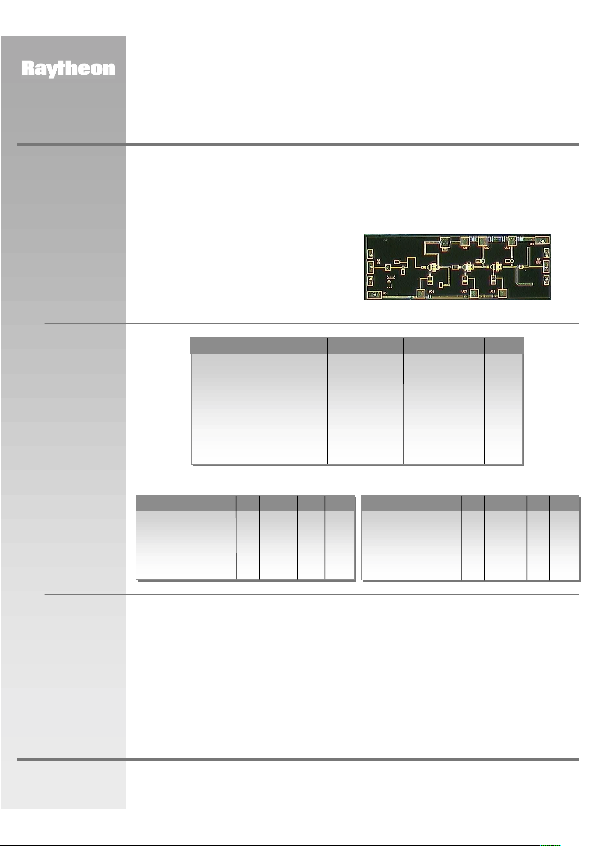
Figure 1
Functional Block
Diagram
Application
Information
MMIC Chip
RF OUT
3Fo
RF IN
Fo
Ground
(Back of Chip)
Gate Supply
(Vg1, Vg2 & Vg3)
Drain Supply
(Vd2)
Drain Supply
(Vd3)
Drain Supply
(Vd1)
X3
0.0
0.974 1.8830.182 2.369
1.019
2.5292.0251.723
0.113
1.007
0.127
3.042
3.111
1.134
0.777
0.577
0.377
0.115
3.224
Figure 2
Chip Layout and Bond
Pad Locations
Chip Size is 3.224 mm x
1.134 mm. Back of chip
is RF ground.
Dimensions in mm
RMTR13390
13-39 GHz Tripler MMIC

Raytheon RF Components
362 Lowell Street
Andover, MA 01810
Revised April 6, 2001
Page 3
www.raytheon.com/micro
Characteristic performance data and specifications are subject to change without notice.
ADVANCED INFORMATION
RF OUT
3Fo
RF IN
Fo
Ground
(Back of Chip)
Gate Supply (Vg)
Drain Supply (Vd = +5 V)
100 pF
10,000 pF
100 pF
10,000 pF
100 pF100 pF
L= Bond Wire Inductance
LL
LLL
L
L
L
L
Figure 3
Recommended
Application Schematic
Circuit Diagram
RMTR13390
13-39 GHz Tripler MMIC
X3
 Loading...