

Raytheon RMPA29000 Datasheet
RMPA29000
27-30 GHz 1 Watt Power
Description
Features
Absolute
Maximum
Ratings
Amplifier MMIC
PRODUCT INFORMATION
The Raytheon RMPA29000 is a high efficiency power amplifier designed for use in point to point radio, point to
multi-point communications, LMDS and other millimeter wave applications. The RMPA29000 is a 3-stage GaAs
MMIC amplifier utilizing Raytheon’s advanced 0.15
µm gate length Power PHEMT process and can be used in
conjunction with other driver or power amplifiers to achieve the required total power output.
23 dB small signal gain (typ.)
30 dBm Pout at 1dB compression (typ.)
Circuit contains individual source Vias
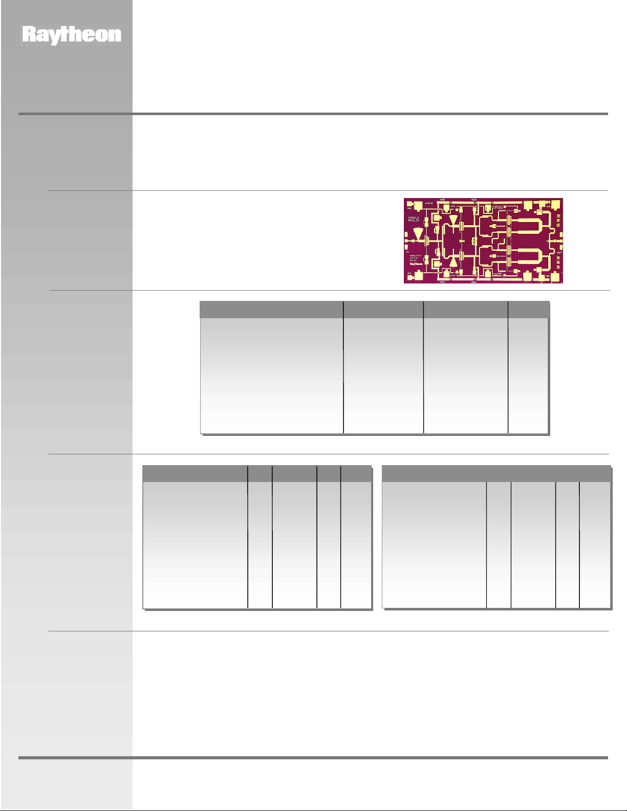
Chip Size 5.20 mm x 2.95 mm
Parameter Symbol Value Unit
Positive DC Voltage (+5 V Typical) Vd
Negative DC Voltage Vg
Simultaneous (Vd - Vg) Vdg + 8 Volts
Positive DC Current I
RF Input Power (from 50 Ω source) P
Operating Base plate Temperature T
Storage Temperature Range T
Thermal Resistance R
(Channel to Backside)
D
IN
C
Stg
jc
+ 6 Volts
- 2 Volts
1092 mA
+18 dBm
-30 to +85 °C
-55 to +125 °C
20 °C/W
Electrical
Characteristics
(At 25°C) 50 Ω system,
Vd=+5 V, Quiescent
current (Idq) = 700 mA
Parameter Min Typ Max Unit
Frequency Range 27 30 GHz
Gate Supply Voltage (Vg)
Gain Small Signal 18 23 dB
(Pin=-1 dBm)
Gain Variation Vs. +/-1 dB
Frequency
Power Output 30 dBm
at 1 dB Compression
Power Output Saturated: 28.5 30.5 dBm
(Pin=+10.5 dBm)
Note:
1. Typical range of the negative gate voltages is -0.9 to 0.0V to set typical Idq of 700 mA.
Characteristic performance data and specifications are subject to change without notice.
1
-0.4 V
Parameter Min Typ Max Unit
Drain Current at 700 mA
Pin=0 dBm
Drain Current 850 mA
at P1 dB Compression
Power Added Efficiency 25 %
(PAE): at P1dB
Input Return Loss 10 dB
(Pin=-1 dBm)
Output Return Loss 10 dB
(Pin=-1 dBm)
www.raytheon.com/micro
Revised January 18, 2001
Page 1
Raytheon RF Components
362 Lowell Street
Andover, MA 01810
RMPA29000
27–30 GHz 1 Watt Power
Application
Information
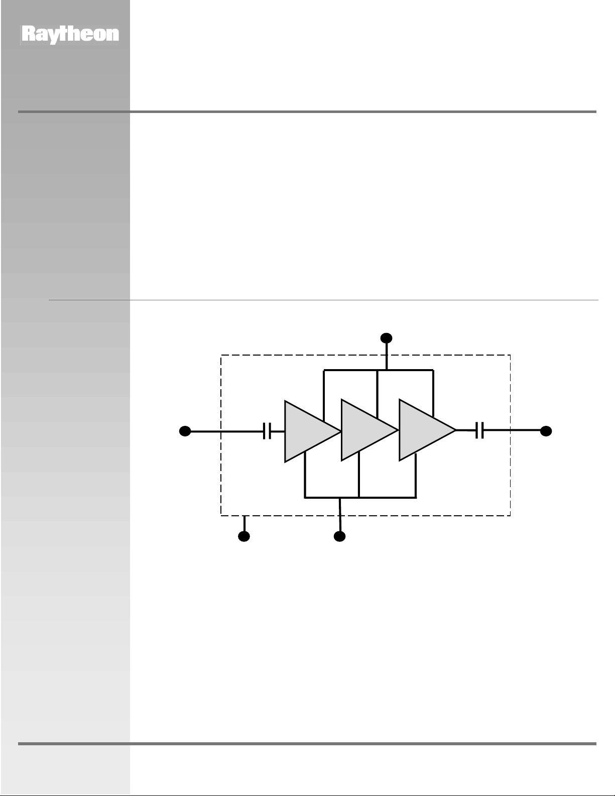
Figure 1
Functional Block
Diagram
Amplifier MMIC
CAUTION: THIS IS AN ESD SENSITIVE DEVICE
Chip carrier material should be selected to have GaAs compatible thermal coefficient of expansion and high
thermal conductivity such as copper molybdenum or copper tungsten. The chip carrier should be machined,
finished flat, plated with gold over nickel and should be capable of withstanding 325°C for 15 minutes.
Die attachment for power devices should utilize Gold/Tin (80/20) eutectic alloy solder and should avoid hydrogen
environment for PHEMT devices. Note that the backside of the chip is gold plated and is used as RF and DC
Ground.
These GaAs devices should be handled with care and stored in dry nitrogen environment to prevent contamination
of bonding surfaces. These are ESD sensitive devices and should be handled with appropriate precaution
including the use of wrist-grounding straps. All die attach and wire/ribbon bond equipment must be well grounded
to prevent static discharges through the device.
Recommended wire bonding uses 3 mils wide and 0.5 mil thick gold ribbon with lengths as short as practical
allowing for appropriate stress relief. The RF input and output bonds should be typically 0.012” long
corresponding to a typically 2 mils gap between the chip and the substrate material.
Drain Supply
(VDA & VDB)
MMIC Chip
PRODUCT INFORMATION
RF IN
Ground
(Back of Chip)
RF OUT
Gate Supply
(VGA & VGB)
www.raytheon.com/micro
Characteristic performance data and specifications are subject to change without notice.
Revised January 18, 2001
Page 2
Raytheon RF Components
362 Lowell Street
Andover, MA 01810
RMPA29000
27–30 GHz 1 Watt Power
Figure 2
Chip Layout and Bond Pad
Locations
(Chip Size=5.210 mm x
2.946 mm x 50
Chip is RF and DC Ground)
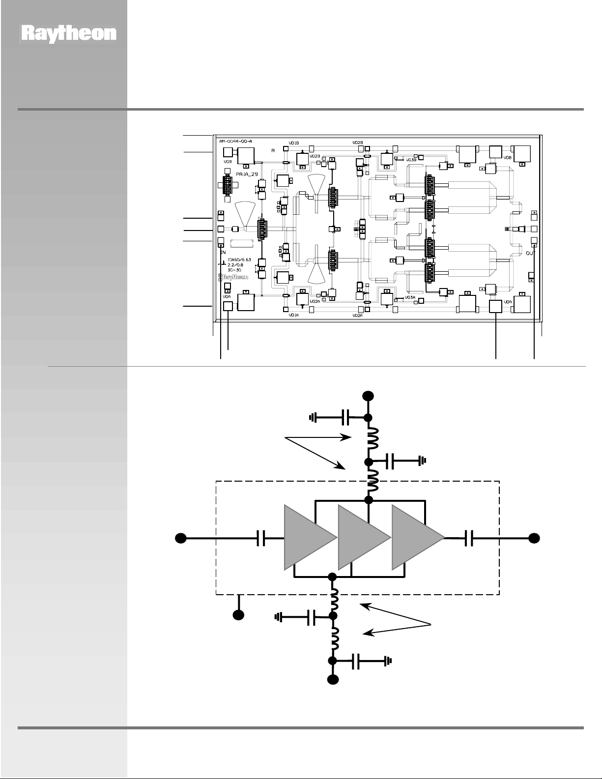
Application Schematic
µm. Back of
Figure 3
Recommended
Circuit Diagram
Amplifier MMIC
Dimensions in mm
2.946
2.672
1.651
1.461
1.285
0.254
0.0
0.122 0.236
PRODUCT INFORMATION
5.210
4.445 5.072
Drain Supply (Vd= +5 V)
(Connect to both VDA & VDB)
10000pF
Bond Wire Ls
MMIC Chip
RF IN
Ground
(Back of Chip)
Characteristic performance data and specifications are subject to change without notice.
100pF
Gate Supply (Vg)
(VGA and/or VGB)
L
L
L
L
10000pF
100pF
RF OUT
Bond Wire Ls
www.raytheon.com/micro
Revised January 18, 2001
Page 3
Raytheon RF Components
362 Lowell Street
Andover, MA 01810
 Loading...