

Raytheon RMPA2451B-58 Datasheet
Raytheon RF Components
362 Lowell Street
Andover, MA 01810
Revised December 7, 2001
Page 1
www.raytheonrf.com
Characteristic performance data and specifications are subject to change without notice.
PRODUCT INFORMATION
Description
38% Power Added Efficiency
29 dBm Typical Output Power
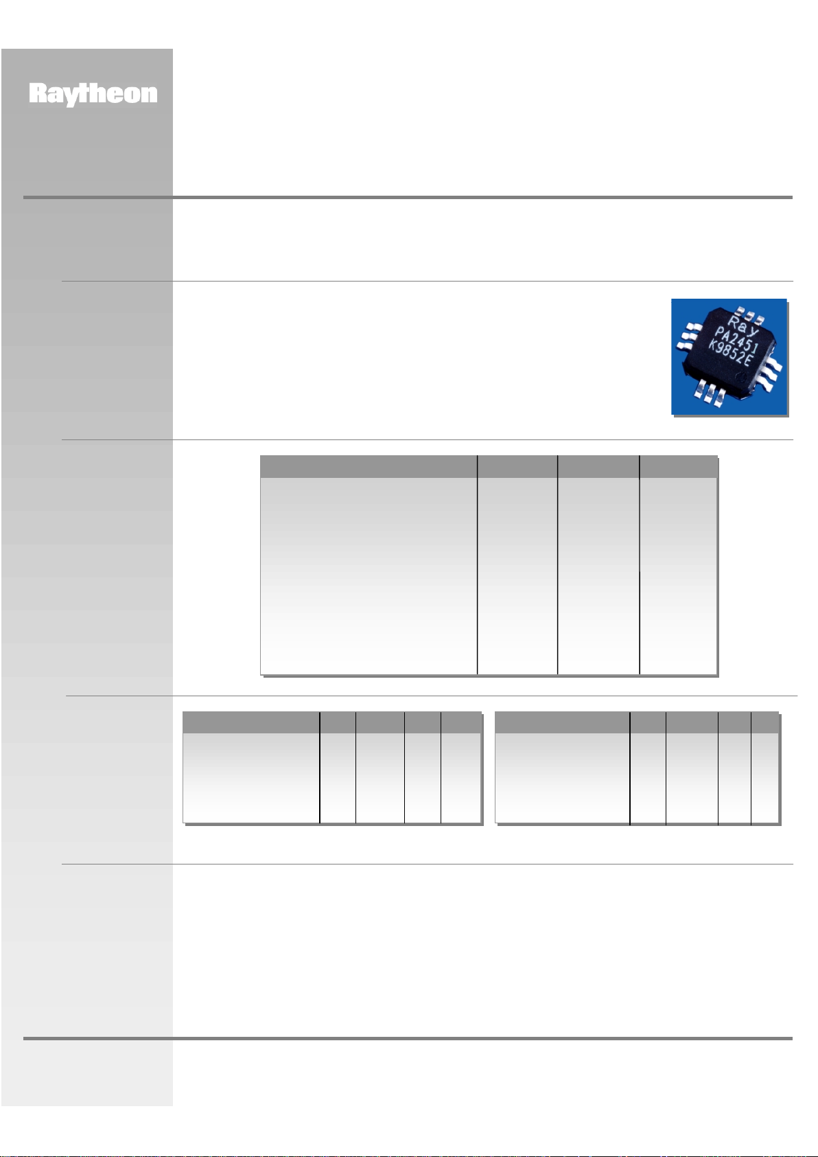
Small package outline: 0.28” x 0.28” x 0.07
Features
Raytheon RMPA2451B-58 is a partially matched monolithic power amplifier in a surface mount package for use in
wireless applications in the 2.4 to 2.5 GHz ISM frequency band. The amplifier may be biased for linear, class AB or
class F for high efficiency applications. External matching components are required to optimize the RF
performance. The MMIC chip design utilizes Raytheon’s 0.25µm power PHEMT process.
Electrical
Characteristics
1
Parameter Min Typ Max Unit
Frequency Range 2400 2450 2500 MHz
Gain
2
28.5 33 dB
Output Power, P1dB
2
27 29 dBm
Associated Power Added
Efficiency 38 %
Parameter Min Typ Max Unit
3rd order Intermod.
Product
3
-35 -27 dBc
Drain Current (Id1 & Id2) 430 mA
Gate Current (Ig1 + Ig2) 5 mA
Input Return Loss (50Ω) -15 dB
Notes:
1. Notes 4, 5. At 25°C using Raytheon Test Boards.
2. Production Testing includes Gain, Output Power at 1-dB gain compression (P1dB) and Input Return Loss at Vd1 = Vd2 = +5.0V;
Vg1,Vg2 = -0.5V (nominal), adjust Vg1 and Vg2 to get Idq1 = 60 mA, Idq2 = 340 mA and at F = 2.45 GHz.
3. Two tone 3rd order Output Intermodulation products (IM3) are measured with total output power level of +25 dBm.
Other Parameters are guaranteed by Design Validation Testing (DVT).
Parameter Symbol Value Units
Positive Drain DC Voltage Vd1,Vd2 +8 Volts
Negative Gate DC Voltage Vg1,Vg2 -5 Volts
Simultaneous Drain to Gate Voltage Vd-Vg +10 Volts
RF Input Power (from 50 Ω source) Pin +10 dBm
Drain Current, First Stage Id1 75 mA
Drain Current, Second Stage Id2 525 mA
Gate Current Ig 5 mA
Channel Temperature Tc 175 °C
Operating Case Temperature Tcase -40 to 85 °C
Storage Temperature Range Tstg -40 to 125 °C
Thermal Resistance (Channel to Case) Rjc 33 °C/Watt
Absolute
Maximum
Ratings
RMPA2451B-58
2.4-2.5 GHz GaAs MMIC
Power Amplifier
Raytheon RF Components
362 Lowell Street
Andover, MA 01810
Revised December 7, 2001
Page 2
www.raytheonrf.com
Characteristic performance data and specifications are subject to change without notice.
PRODUCT INFORMATION
CAUTION: THIS IS AN ESD SENSITIVE DEVICE.
The following describes the procedure for evaluating the RMPA2451B-58, a partially-matched Pseudomorphic High
Electron Mobility (PHEMT) monolithic power amplifier which has been designed for wireless applications in the 2.4
- 2.5 GHz ISM band, in a surface mount package. The package outline, along with the pin designations, is provided
as Figure 1. The functional block diagram of the packaged product is provided as Figure 2.
It should be noted that the RMPA2451B-58 requires the use of external passive components to form the DC bias
and RF output matching circuits. The schematic for a recommended DC bias / RF matching circuit is shown in
Figure 3, along with a list of the appropriate components. Figure 2 illustrates the layout of an evaluation board
based on this schematic (RMPA2451B-58-TB).
Figures 5 to 7 illustrate typical device performance. This data for various operating parameters was obtained
across the design bandwidth over a range of temperatures.
Figure 5 shows the variation in Gain and P1dB with temperature and operating frequency.
Figure 6 shows the 3rd-order intermodulation product measured at different total output power levels.
Figure 7 demonstrates the device performance under a Wideband Code Division Multiple Access (W-CDMA)
modulation scheme, the conditions of which are specified.
Application
Information
Pins #1, #2, #3
RF OUTPUT & Vd2
Pin #10
V
g1
Pin #11
V
g2
Package Underside
GROUND
Figure 2
Functional Block
Diagram
Figure 1
Package
Information
BOTTOM VIEW
0.041
Vd2 + RF Out
Vd2 + RF Out
Vd2 + RF Out
GND
Vd1
GND
GND
RF In
GND
Vg1
Vg2
GND
GND
1
2
3
4
5
6
7
8
9
10
11
12
BASE
Description
Pin #
Dimensions in inches
SIDE SECTION
0.070 MAX.
PLASTIC LID
0.010
0.230
0.246
0.282
10
11
TOP VIEW
0.030
0.015
1
2
3
456
7
8
9
12
0.200 SQ.
Raytheon
RMPA2451B-58
PPYYWWX
Pins #4, #6, #7, #9, #12
Ground
Pin #5
V
d1
Pin #8
RF INPUT
RMPA2451B-58
2.4-2.5 GHz GaAs MMIC
Power Amplifier
Raytheon RF Components
362 Lowell Street
Andover, MA 01810
Revised December 7, 2001
Page 3
www.raytheonrf.com
Characteristic performance data and specifications are subject to change without notice.
PRODUCT INFORMATION
Step 1: Turn the RF power OFF.
Step 2: Use the GND terminals of the evaluation board
for the ground of the DC supplies.
Step 3: Apply a nominal voltage of approximately -1.5V
to both V
gg1
and V
gg2
terminals.
Step 4: Apply a nominal voltage of +5.0V to the V
dd
terminals. Adjust V
gg1
to give a first stage
quiescent Drain current, I
d1
of 60mA. Adjust
V
gg2
to provide a second stage quiescent Drain
current, I
dd2
, of 340 mA.
Step 5: Apply an RF signal within the ISM frequency
range (2.4 - 2.5 GHz) at an initial input power
level of -10 dBm.
Step 6: To perform intermodulation product
measurements, a second RF signal generator
with a frequency difference of 1 MHz is
required, along with an appropriate power
combiner. The test configuration should
allow this additional generator to provide the
same input power level as the first generator
into the device. Intermodulation readings
may then be made at the required total
output power levels.
Step 7: To operate at lower quiescent Drain currents,
increase the magnitudes of V
gg1
and V
gg2
as
required, alternatively to operate at higher
quiescent Drain currents, the magnitudes of
V
gg1
and V
gg2
should be decreased
accordingly.
Step 8: When turning the amplifier OFF, the power-
up sequence should be reversed.
Figure 3
Schematic of a
recommended DC bias/
RF matching circuit
V
g1
C
2
C
1
Raytheon
RMPA2451B
PPYYWWX
V
d1
V
g2
C
2
C
1
C
2
C
1
V
d2
L
1
C
4
RF Output
RF Input
C
3
C
3
C
2
C
1
L
2
It is important that the following points be noted prior to testing; Pin designations are as shown in Figure 2.
V
gg1
and V
gg2
are the negative Gate bias voltages applied at the pins of the evaluation test board.
V
dd1
and V
dd2
are the positive Drain bias voltages applied at the pins of the evaluation test board.
V
g1
and Vg2 are the negative Gate bias voltages applied at the pins of the package.
V
d1
and Vd2 are the positive Drain bias voltages applied at the pins of the package.
Test Procedure
for the
evaluation board
(RMPA2451B-58-TB)
CAUTION: LOSS OF GATE VOLTAGE (VG1, VG2) WHILE DRAIN VOLTAGES (VD1, VD2) ARE PRESENT MAY
DAMAGE THE AMPLIFIER.
The following sequence of procedures must be followed to properly test the amplifier:
RMPA2451B-58
2.4-2.5 GHz GaAs MMIC
Power Amplifier
 Loading...